WO2024247904A1 - 伸縮性デバイス - Google Patents
伸縮性デバイス Download PDFInfo
- Publication number
- WO2024247904A1 WO2024247904A1 PCT/JP2024/019140 JP2024019140W WO2024247904A1 WO 2024247904 A1 WO2024247904 A1 WO 2024247904A1 JP 2024019140 W JP2024019140 W JP 2024019140W WO 2024247904 A1 WO2024247904 A1 WO 2024247904A1
- Authority
- WO
- WIPO (PCT)
- Prior art keywords
- stretchable
- electrode portion
- view
- plan
- wiring
- Prior art date
- Legal status (The legal status is an assumption and is not a legal conclusion. Google has not performed a legal analysis and makes no representation as to the accuracy of the status listed.)
- Ceased
Links
Images


Classifications
-
- H—ELECTRICITY
- H05—ELECTRIC TECHNIQUES NOT OTHERWISE PROVIDED FOR
- H05K—PRINTED CIRCUITS; CASINGS OR CONSTRUCTIONAL DETAILS OF ELECTRIC APPARATUS; MANUFACTURE OF ASSEMBLAGES OF ELECTRICAL COMPONENTS
- H05K1/00—Printed circuits
- H05K1/02—Details
- H05K1/11—Printed elements for providing electric connections to or between printed circuits
- H05K1/115—Via connections; Lands around holes or via connections
-
- H—ELECTRICITY
- H05—ELECTRIC TECHNIQUES NOT OTHERWISE PROVIDED FOR
- H05K—PRINTED CIRCUITS; CASINGS OR CONSTRUCTIONAL DETAILS OF ELECTRIC APPARATUS; MANUFACTURE OF ASSEMBLAGES OF ELECTRICAL COMPONENTS
- H05K1/00—Printed circuits
- H05K1/02—Details
- H05K1/0277—Bendability or stretchability details
- H05K1/0283—Stretchable printed circuits
-
- H—ELECTRICITY
- H05—ELECTRIC TECHNIQUES NOT OTHERWISE PROVIDED FOR
- H05K—PRINTED CIRCUITS; CASINGS OR CONSTRUCTIONAL DETAILS OF ELECTRIC APPARATUS; MANUFACTURE OF ASSEMBLAGES OF ELECTRICAL COMPONENTS
- H05K1/00—Printed circuits
- H05K1/02—Details
-
- H—ELECTRICITY
- H05—ELECTRIC TECHNIQUES NOT OTHERWISE PROVIDED FOR
- H05K—PRINTED CIRCUITS; CASINGS OR CONSTRUCTIONAL DETAILS OF ELECTRIC APPARATUS; MANUFACTURE OF ASSEMBLAGES OF ELECTRICAL COMPONENTS
- H05K1/00—Printed circuits
- H05K1/02—Details
- H05K1/11—Printed elements for providing electric connections to or between printed circuits
- H05K1/118—Printed elements for providing electric connections to or between printed circuits specially for flexible printed circuits, e.g. using folded portions
-
- H—ELECTRICITY
- H05—ELECTRIC TECHNIQUES NOT OTHERWISE PROVIDED FOR
- H05K—PRINTED CIRCUITS; CASINGS OR CONSTRUCTIONAL DETAILS OF ELECTRIC APPARATUS; MANUFACTURE OF ASSEMBLAGES OF ELECTRICAL COMPONENTS
- H05K3/00—Apparatus or processes for manufacturing printed circuits
- H05K3/46—Manufacturing multilayer circuits
Definitions
- the present invention relates to a stretchable device.
- a stretchable device has been known that includes a stretchable substrate, a first stretchable wiring disposed on the stretchable substrate, and a second stretchable wiring disposed on the first stretchable wiring and connected through a via.
- the inventors of the present application have found that the following points need to be improved in conventional stretchable devices. Specifically, if the positional accuracy between the via used to interconnect two stretchable wires and the electrode part of the upper second stretchable wire is not consistent, it may be difficult to improve the connection reliability between the electrode part of the lower first stretchable wire and the electrode part of the upper second stretchable wire. In particular, when the entire device stretches and contracts, as in the case of a stretchable device, misalignment is likely to occur, and therefore high connection reliability is required.
- the present invention aims to provide a stretchable device that can improve the connection reliability between the electrode portions of two adjacent stretchable wirings.
- a stretchable device is provided, wherein the first via portion partially has a connection region connecting between the first electrode portion and the second electrode portion.
- the stretchable device makes it possible to improve the connection reliability between the electrode portions of two adjacent stretchable wirings.
- FIG. 1 is a plan view illustrating a stretchable device according to a first embodiment of the present invention.
- FIG. 2A is a plan view illustrating a stretchable device according to a second embodiment of the present invention.
- FIG. 2B is a plan view illustrating a modified example of the stretchable device according to the second embodiment of the present invention.
- FIG. 3A is a plan view that illustrates step 1 of the method for producing a stretchable device according to a second embodiment of the present invention.
- FIG. 3B is a plan view that illustrates step 2 of the method for producing a stretchable device according to the second embodiment of the present invention.
- FIG. 3C is a plan view that illustrates step 3 of the method for producing a stretchable device according to the second embodiment of the present invention.
- FIG. 1 is a plan view illustrating a stretchable device according to a first embodiment of the present invention.
- FIG. 2A is a plan view illustrating a stretchable device according to a second embodiment of the present invention.
- FIG. 3D is a plan view that illustrates step 4 of the method for producing a stretchable device according to the second embodiment of the present invention.
- FIG. 3E is a plan view that illustrates step 5 of the method for producing a stretchable device according to the second embodiment of the present invention.
- FIG. 4A is a plan view that illustrates step 1 of a method for producing a modified stretchable device according to the second embodiment of the present invention.
- FIG. 4B is a plan view that illustrates step 2 of the method for producing a modified example of the stretchable device according to the second embodiment of the present invention.
- FIG. 4C is a plan view that illustrates step 3 of the method for producing a modified example of the stretchable device according to the second embodiment of the present invention.
- FIG. 4D is a plan view that illustrates step 4 of the method for producing a modified example of the stretchable device according to the second embodiment of the present invention.
- FIG. 4E is a plan view that illustrates step 5 of the method for producing a modified example of the stretchable device according to the second embodiment of the present invention.
- FIG. 5 is a plan view illustrating a stretchable device according to a third embodiment of the present invention.
- FIG. 6A is a plan view diagrammatically illustrating a first modified example of a stretchable device according to the third embodiment of the present invention.
- FIG. 6B is a cross-sectional view that illustrates a schematic structure between AA in FIG. 6A.
- FIG. 7A is a plan view diagrammatically illustrating a second modified example of the stretchable device according to the third embodiment of the present invention.
- FIG. 7B is a cross-sectional view that illustrates a schematic structure taken along line BB in FIG. 7A.
- FIG. 8A is a plan view diagrammatically illustrating a third modified example of the stretchable device according to the third embodiment of the present invention.
- FIG. 8B is a cross-sectional view that illustrates a schematic structure between AA in FIG. 8A.
- FIG. 8C is a cross-sectional view that illustrates the structure between B-B in FIG. 8A.
- FIG. 9A is a plan view diagrammatically illustrating a fourth modified example of the stretchable device according to the third embodiment of the present invention.
- FIG. 9A is a plan view diagrammatically illustrating a fourth modified example of the stretchable device according to the third embodiment of the present invention.
- FIG. 9B is a cross-sectional view that illustrates a schematic structure between AA in FIG. 9A.
- FIG. 9C is a cross-sectional view that illustrates a schematic structure between B-B in FIG. 9A.
- FIG. 10A is a plan view diagrammatically illustrating a fifth modified example of the stretchable device according to the third embodiment of the present invention.
- FIG. 10B is a cross-sectional view that illustrates a schematic structure between AA in FIG. 10A.
- FIG. 10C is a cross-sectional view that illustrates a schematic structure between B-B in FIG. 10A.
- FIG. 11A is a plan view diagrammatically illustrating a sixth modified example of the stretchable device according to the third embodiment of the present invention.
- FIG. 11A is a plan view diagrammatically illustrating a sixth modified example of the stretchable device according to the third embodiment of the present invention.
- FIG. 11B is a cross-sectional view that illustrates a schematic structure between AA in FIG. 11A.
- FIG. 12A is a plan view diagrammatically illustrating a seventh modified example of the stretchable device according to the third embodiment of the present invention.
- FIG. 12B is a cross-sectional view that illustrates a schematic structure between AA in FIG. 12A.
- FIG. 13A is a plan view that illustrates step 1 of the method for producing a stretchable device according to the third embodiment of the present invention.
- FIG. 13B is a plan view that illustrates step 2 of the method for producing a stretchable device according to the third embodiment of the present invention.
- FIG. 13C is a plan view that illustrates step 3 of the method for producing a stretchable device according to the third embodiment of the present invention.
- FIG. 12A is a plan view diagrammatically illustrating a seventh modified example of the stretchable device according to the third embodiment of the present invention.
- FIG. 12B is a cross-sectional view that illustrate
- FIG. 13D is a plan view that illustrates step 4 of the method for producing a stretchable device according to the third embodiment of the present invention.
- FIG. 13E is an enlarged plan view that illustrates step 5 of the method for producing a stretchable device according to the third embodiment of the present invention.
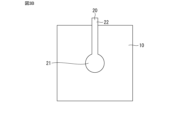
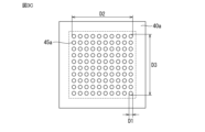
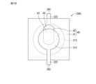
- Fig. 1 is a plan view diagrammatically illustrating a stretchable device according to an embodiment of the present invention.
- the stretchable device 100 comprises a stretchable substrate, a first stretchable wiring 20 disposed on the stretchable substrate, a second stretchable wiring 30 disposed on the first stretchable wiring 20, and an interlayer sheet 40 disposed between the first stretchable wiring 20 and the second stretchable wiring 30.
- above includes a state where it is located above an element and separated from it, i.e., above an element via another object, a state where it is located above an element with a gap, and a state where it is located directly above an element and in contact with it.
- the "first elastic wiring 20 disposed on the elastic substrate” includes the first elastic wiring 20 in contact with the main surface of the elastic substrate, and the first elastic wiring 20 in a state where it is separated from the main surface via another member (for example, a resin layer described below) without directly contacting the main surface of the elastic substrate.
- the resin layer may be formed of at least one resin material selected from the group consisting of polyimide-based, epoxy-based, urethane-based, and acrylic-based resins.
- the resin layer may also be formed of an inorganic material such as alumina or silicon dioxide.
- the stretchable substrate is a sheet-like or film-like stretchable substrate, and is made of, for example, a resin material having stretchability.
- resin materials for the stretchable substrate include thermoplastic polyurethane (TPU), styrene-based elastomer, polyethylene (PE), polystyrene (PS), polyethylene terephthalate (PET), etc.
- the thickness of the elastic substrate is not particularly limited, but from the viewpoint of not inhibiting the expansion and contraction of the surface of the living body when attached to the living body, it is preferably 100 ⁇ m or less, and more preferably 50 ⁇ m or less. In addition, from the viewpoint of ensuring a certain strength, the thickness of the elastic substrate is preferably 20 ⁇ m or more.
- the first elastic wiring 20 and the second elastic wiring 30 each contain conductive particles and a resin.
- each elastic wiring may be a mixture of metal powder such as Ag, Cu, Ni, etc. as conductive particles and an elastomer resin such as a silicone resin.
- the average particle size of the conductive particles is not particularly limited, but is preferably 0.01 ⁇ m or more and 10 ⁇ m or less.
- the conductive particles are preferably spherical in shape.
- each elastic wire is not particularly limited, but is preferably 100 ⁇ m or less, and more preferably 50 ⁇ m or less.
- the thickness of each elastic wire is preferably 0.01 ⁇ m or more.
- the line width of each elastic wire is not particularly limited, but is preferably 0.1 ⁇ m or more, and more preferably 10 mm or less.
- the shape, etc. of each elastic wire is not particularly limited.
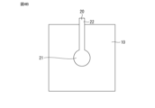
- the first elastic wiring 20 has a first electrode portion 21 and a first extension portion 22 extending from the first electrode portion 21 in a predetermined direction.
- the second elastic wiring 30 has a second electrode portion 31 and a second extension portion 32 extending from the second electrode portion 31 in a predetermined direction. In a planar view, the first electrode portion 21 and the second electrode portion 31 overlap each other.
- the first extension portion 22 and the second extension portion 32 may extend in opposite directions to each other. Without being limited thereto, the first extension portion 22 and the second extension portion 32 may extend in the same direction.
- the first electrode portion 21 and the second electrode portion 31 can have the same size and shape in a plan view.
- the planar shape of each electrode portion can be, for example, a perfect circle, an ellipse, or other circular shape, a polygon, etc.
- the planar sizes of these components do not necessarily have to be the same, and the first electrode portion 21 located on the lower layer side may be larger than the second electrode portion 31, and the elastic substrate located on the lower layer side may be larger than the interlayer sheet. Furthermore, the planar shapes of these components do not necessarily have to be the same.
- the interlayer sheet 40 includes a sheet portion 41 and at least one first via portion 42 provided in the sheet portion 41.
- the interlayer sheet 40 may be made of the same material and thickness as the above-mentioned stretchable substrate.
- the stretchable substrate and the interlayer sheet may also have the same size and shape.
- the planar shapes of the stretchable substrate and the interlayer sheet may be, for example, rectangular, square, polygonal, etc.
- the present invention is characterized in that the first via portion 42 partially has a connection region 43 that connects between the first electrode portion 21 and the second electrode portion 31.
- the first via portion 42 has a non-connection region 44 that does not connect the first electrode portion 21 and the second electrode portion 31. That is, in a plan view (when viewed in the thickness direction of the elastic substrate), the second electrode portion 31 overlaps a portion of the first via portion 42.
- the entire first via portion 42 is not composed of the connection region 43, but rather a portion of the first via portion 42 constitutes the connection region 43, and the remaining portion constitutes the non-connection region 44 that does not connect between the first electrode portion 21 and the second electrode portion 31.
- the position of the second electrode portion 31 is such that the above-mentioned connection region 43 and non-connection region 44 are provided, and the overall positional relationship between the first via portion 42 and the second electrode portion 31 can be determined.
- the stretchable device 100 may further include an adhesive layer.
- the adhesive layer has adhesiveness that allows the stretchable device 100 to be attached to an adherend such as a living body.
- the adhesive layer may be positioned between the stretchable substrate and the adherend such as a living body.
- the adhesive layer has a first main surface facing the adherend, such as a living body, and a second main surface on the opposite side.
- the first adhesive layer preferably has adhesiveness on both main surfaces.
- the first main surface of the adhesive layer can be attached to a living body, etc.
- the second main surface of the adhesive layer can be attached to a stretchable substrate.
- a protective layer may further be disposed between the second main surface of the adhesive layer and the stretchable substrate from the viewpoint of improving waterproofing, etc.
- the adhesive layer there are no particular restrictions on the adhesive layer, so long as it is an adhesive that is mild to the skin, has sufficient pressure-sensitive adhesive properties, and can be easily peeled off from the skin after use.
- the adhesive layer may be composed of a pressure-sensitive adhesive or the like, although it is not particularly limited.
- a pressure-sensitive adhesive there is no particular limit to the pressure-sensitive adhesive, so long as it is one that can be generally used by laminating it on an elastic substrate.
- rubber-, acrylic-, or silicone-based pressure-sensitive adhesives can be used.
- a pressure-sensitive adhesive When a pressure-sensitive adhesive is used, it can be bonded to the opposing member (elastic substrate) at a relatively low temperature, so that it is possible to prevent deterioration or distortion of the elastic substrate by using excessive heat or UV energy.
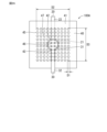
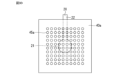
- Fig. 2A is a plan view diagrammatically illustrating the stretchable device according to the second embodiment of the present invention.
- the second embodiment differs from the first embodiment in that the interlayer sheet 40 includes a plurality of via portions 45.
- the via portions 45 have a planar size smaller than each electrode portion.
- the planar size of the via portions 45 is also smaller than the width (short dimension) of the extension portion of each wiring.
- they can be regularly arranged at predetermined intervals on the sheet portion 41 in a planar view.
- An example of a regular arrangement is a matrix arrangement.
- the interlayer sheet 40 has a collection of via portions 45.
- the planar shape of the via portion 45 may be, for example, a circle, an ellipse, or other circular shape, or a polygonal shape.
- its diameter size D1 is, for example, 10 ⁇ m or more and 500 ⁇ m or less, and may be, for example, 50 ⁇ m or more and 300 ⁇ m or less, taking into account ease of material filling.
- their vertical and horizontal sizes D2 and D3 are, respectively, 2 mm or more and 20 mm or less, and may be, for example, 5 mm.
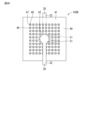
- the multiple via portions 45 include a second via portion 46 and a third via portion 47 in addition to the first via portion 42 described in the first embodiment. There may be two or more of each of the first to third via portions.
- the first via portion 42 is a via portion that partially has a connection region that connects between the first electrode portion 21 and the second electrode portion 31.
- the first via portion 42 is a via portion that partially overlaps with the second electrode portion 31 in a plan view.
- the first via portion 42 corresponds to the partially shaded via portion of one via.
- the second via portion 46 may be a via portion that overlaps entirely with the second electrode portion 31 in a plan view.
- the second via portion 46 corresponds to the via portion that is entirely shaded in one via.
- the second via portion 46 may be a via portion that partially overlaps with the second electrode portion 31 in a plan view.
- the second via portion 46 consists of a connection region that connects between the first electrode portion 21 and the second electrode portion 31.
- the second via portion 46 does not need to have a non-connected region that does not connect the first electrode portion 21 and the second electrode portion 31. Furthermore, the second via portion 46 contacts the second electrode portion 31 and is located below the second electrode portion 31. The presence of such a second via portion 46 can improve the connection reliability between the two electrode portions.
- FIG. 2A used in this embodiment and the corresponding FIG. 3E described below the second via portion located below the second electrode portion is shown with a dotted line to improve understanding of the positional relationship and configuration of the second via portion.
- the second via portion located below the second electrode portion is not shown in consideration of the ease of viewing each drawing.
- the third via portion 47 is a via portion that does not overlap with the second electrode portion 31 in a plan view.
- the third via portion 47 may be a via hole.
- the third via portion 47 corresponds to the non-shaded via portion of one via.
- the planar size of the via portion 45 is smaller than the planar size of each electrode portion. Therefore, in a planar view, multiple via portions 45, specifically, the connection regions of multiple first via portions and multiple second via portions 46, can be positioned between the first electrode portion 21 and the second electrode portion 31.
- the planar size of the via portion 45 is smaller than the width (short dimension) of the extension portion of each wiring, so that it is possible to avoid breakage originating from the portion where the second extension portion 32 of the second elastic wiring 30 overlaps with the edge of the via portion 45 in a planar view.
- connection regions between the first electrode portion 21 and the second electrode portion 31 that connect these electrode portions, these multiple connection regions can provide an anchor effect for the second electrode portion 31. This can improve the adhesion between the second electrode portion 31 and the interlayer sheet 40 that has multiple connection regions.
- the following describes a method for producing the stretchable device 100A according to the second embodiment.
- Step 1 3A is a plan view that illustrates step 1 of the method for producing a stretchable device according to the second embodiment of the present invention.
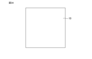
- a stretchable substrate 10 is prepared.
- Step 2 3B is a plan view showing step 2 of the method for producing a stretchable device according to the second embodiment of the present invention.
- a wiring material is screen-printed on the stretchable substrate 10 using a squeegee or the like, and then dried at about 100° C. for a predetermined time. This allows the first stretchable wiring 20 to be formed on the stretchable substrate 10.
- Step 3 3C is a plan view showing step 3 of the method for producing a stretchable device according to the second embodiment of the present invention.
- a substrate 40a to be used as an interlayer sheet is prepared.
- This substrate 40a may be the same as the stretchable substrate 10 described above.
- a laser is irradiated onto this substrate 40a at a predetermined interval to form via holes 45a having a regular arrangement such as a matrix arrangement.
- the laser for example, a carbon dioxide laser can be used.
- the planar shape of the via hole 45a may be, for example, a circle, an ellipse, or other circular shape, or a polygon.
- its diameter size D1 may be, for example, 10 ⁇ m or more and 500 ⁇ m or less.
- its vertical and horizontal sizes D2 and D3 may be, for example, 2 mm or more and 20 mm or less.
- Step 4 Fig. 3D is a plan view showing step 4 of the method for producing a stretchable device according to the second embodiment of the present invention.
- the substrate 40a prepared in the same step is bonded to the stretchable substrate 10 with the first stretchable wiring 20.
- a bonding means for example, dry lamination using a vacuum press machine can be mentioned.
- Step 5 3E is a plan view showing step 5 of the method for producing a stretchable device according to the second embodiment of the present invention.
- a wiring material is screen-printed at a predetermined location of the base material 40a as an interlayer sheet using a squeegee or the like so as to be interlayer-connectable with the first electrode portion 21 of the first stretchable wiring 20 through the via hole 45a.
- the substrate is dried at about 100° C. for a predetermined time.
- the second stretchable wiring 30 can be formed on the obtained interlayer sheet 40.
- the through holes formed in the substrate 40a during the intermediate manufacturing stage are referred to as via holes 45a, and when manufacturing is complete, they are referred to as via portions 45.
- the reason for using these different expressions is that the obtained via portions 45 include a first via portion 42 (partially filled with wiring material), a second via portion 46 (completely filled with wiring material), and a third via portion (not filled with wiring material and remaining in the form of a via hole).
- Fig. 2B is a plan view diagrammatically illustrating a modified example of the stretchable device according to the second embodiment of the present invention.
- the modified example of the second embodiment differs from the second embodiment in that the via portion 45 already has a conductive material 48 inside.
- the conductive material may be the same as the wiring material described above.
- the fact that the conductive material is already provided inside the via portion 45 means that, at a stage before the second elastic wiring is formed, the conductive material is already provided in at least the portion that will become the third via portion as well as the portion that will become the second via portion that may overlap with the second electrode portion.
- the third via portion 47 after formation corresponds to a via portion that is generally shaded in a different direction in one via portion compared to the second via portion 46 shown in FIG. 2A.
- the following describes a method for producing the stretchable device 100B according to the second embodiment (a modified example of the second embodiment). Note that explanations of parts that overlap with those described in the section on the method for producing the stretchable device 100A will be omitted or simplified.
- Step 1 4A is a plan view that illustrates a schematic diagram of step 1 of a method for producing a modified stretchable device according to the second embodiment of the present invention.
- a stretchable substrate 10 is prepared.
- Step 2 4B is a plan view showing step 2 of the method for producing a modified stretchable device according to the second embodiment of the present invention.
- a wiring material is screen-printed on the stretchable substrate 10 and then dried. This allows the first stretchable wiring 20 to be formed on the stretchable substrate 10.
- FIG. 4C is a plan view showing step 3 of the method for producing a modified stretchable device according to the second embodiment of the present invention.
- a base material 40a to be used as an interlayer sheet is prepared.
- a laser is irradiated to the base material 40a at a predetermined interval to form a plurality of regularly arranged via holes 45a.
- a conductive material is then filled at predetermined locations of the plurality of via holes 45a.
- the conductive material can be filled in the via holes by using screen printing.
- the filling location at least the portion that will become the third via portion and the portion that will become the second via portion in the finally obtained device are filled in advance with a conductive material.
- Step 4 Fig. 4D is a plan view showing step 4 of the method for producing a modified stretchable device according to the second embodiment of the present invention.
- the base material 40a prepared in the same step is bonded to the stretchable base material 10 with the first stretchable wiring 20.
- a conductive material may be filled in predetermined locations of the multiple via holes 45a.
- Step 5 4E is a plan view showing step 5 of the method for producing a modified stretchable device according to the second embodiment of the present invention.
- step 4 is performed, similar to step 2, a wiring material is screen-printed at a predetermined location of the base material 40a as an interlayer sheet so as to be capable of interlayer connection with the first electrode portion 21 of the first stretchable wiring 20 through the via hole 45a.
- the substrate is dried.
- the second stretchable wiring 30 can be formed on the obtained interlayer sheet 40.
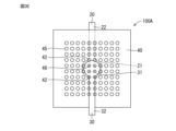
- Fig. 5 is a plan view diagrammatically illustrating the stretchable device according to the third embodiment of the present invention.
- the stretchable device 100C in the third embodiment has basically the same configuration as the first embodiment.
- the difference from the first embodiment is, for example, that the planar size of the second electrode portion 31C of the second stretchable wiring 30C is smaller than the planar size of the first electrode portion 21C of the first stretchable wiring 20C, as shown in FIG. 5.
- the position of the second electrode portion 31C is such that the above-mentioned connection region 43 and non-connection region 44 are provided, and the positional relationship between the first via portion 42 and the second electrode portion 31C as a whole can be determined.
- the wiring material is formed so as not to cover or overlap the entire via hole in a planar view. This makes it possible to secure an escape route for the air located in the via hole, and to suppress the occurrence of residual air bubbles (also called smears) in the via portion including the connection region 43 made of the obtained wiring material (corresponding to a conductive material).
- FIG. 6A is a plan view showing a first modified example of a stretchable device according to a third embodiment of the present invention.
- FIG. 6B is a cross-sectional view showing a structure between A-A in FIG. 6A.
- Variation 1 is characterized in that, in a plan view, the non-connected region 44D of the first via portion 42D extends from the second electrode portion 31D toward the edge portion 41DI of the interlayer sheet 40D. Also, as shown in the figure, each of the first elastic wiring 20D and the second elastic wiring 30D has two or more electrode portions 21D, 31D.
- This feature allows the orientation of the non-connected region 44D of the first via portion 42D to be constant. It also makes it easier to ensure a sufficient size of the non-connected region 44D between the electrode portion and the edge portion 41DI of the interlayer sheet 40D. As a result, the positional relationship between the first via portion 42D and the second electrode portion 31D can be made clearer. This makes it possible to more appropriately ensure the positional accuracy of the first via portion 42D and the second electrode portion 31D.
- the second stretchable wiring 30D when forming the second stretchable wiring 30D during the production of the stretchable device 100D, it becomes easier to secure an escape route for the air located in the via hole, and the occurrence of air bubbles remaining in the via portion including the connection region 43D made of the resulting wiring material (corresponding to the conductive material) can be further suppressed.
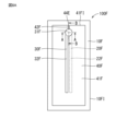
- FIG. 7A is a plan view showing a second modified example of a stretchable device according to the third embodiment of the present invention.
- FIG. 7B is a cross-sectional view showing a structure between B-B in FIG. 7A.
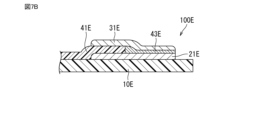
- Variation 2 is characterized in that, in plan view, the non-connected region 44E of the first via portion 42E continues from the second electrode portion 31E to the edge portion 41EI of the interlayer sheet 40E.
- the interlayer sheet 40E is partially divided with the non-connected region 44E of the first via portion 42E as the base point.
- the expansion and contraction force acts in the direction of the arrow shown in FIG. 7A
- the expansion and contraction force is less likely to act on the expandable wiring located in the center of the expandable device 100E in a planar view.
- This makes it possible to suppress the expansion and contraction of the wiring, and reduce changes in wiring resistance.
- cutting debris is less likely to remain in the via portion. This makes it easier to ensure that the size of the via portion is a specified size.
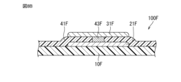
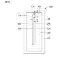
- FIG. 8A is a plan view showing a schematic diagram of a third modified example of a stretchable device according to the third embodiment of the present invention.
- FIG. 8B is a cross-sectional view showing a schematic diagram of the structure between A-A in FIG. 8A.
- FIG. 8C is a cross-sectional view showing a schematic diagram of the structure between B-B in FIG. 8A.
- Variation 3 is characterized in that, in plan view, edge 41FI of interlayer sheet 40F is located inside edge 10FI of stretchable substrate 10F.
- the planar size of interlayer sheet 40F is smaller than the planar size of stretchable substrate 10F, so high precision joining is not required when joining interlayer sheet 40F to stretchable substrate 10F, which is preferable in terms of manufacturing efficiency.
- a stretchable device even if there is external contact in the longitudinal extension direction of the substrate, direct contact of interlayer sheet 40F can be avoided.
- FIG. 9A is a plan view showing a fourth modified example of a stretchable device according to the third embodiment of the present invention.
- FIG. 9B is a cross-sectional view showing a structure between A-A in FIG. 9A.
- FIG. 9C is a cross-sectional view showing a structure between B-B in FIG. 9A.
- Variation 4 is characterized in that three or more elastic wires are arranged in the thickness direction of the elastic substrate 10G, and the electrode portion of one adjacent elastic wire and the electrode portion of the other adjacent elastic wire are connected to each other through the first via portion 42G of the interlayer sheet 40G.
- the stretchable device 100G has a first stretchable wiring 20G, a second stretchable wiring 30G, and a third stretchable wiring 50G arranged between the first stretchable wiring 20G and the second stretchable wiring 30G in the thickness direction of the stretchable substrate 10.
- the positional relationship between the first via portion 42G and the second electrode portion 31G as a whole can be determined. This makes it possible to ensure the positional accuracy of the first via portion 42G and the second electrode portion 31G.
- the wiring material is formed so as not to cover or overlap the entire via hole in a plan view. This ensures an escape route for the air located in the via hole, and makes it possible to suppress the occurrence of residual air bubbles (also called smears) in the via portion including the connection region 43G made of the resulting wiring material (corresponding to a conductive material).
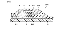
- FIG. 10A is a plan view showing a schematic diagram of a fifth modified example of a stretchable device according to the third embodiment of the present invention.
- FIG. 10B is a cross-sectional view showing a schematic diagram of the structure between A-A in FIG. 10A.
- FIG. 10C is a cross-sectional view showing a schematic diagram of the structure between B-B in FIG. 10A.
- variant 5 is characterized in that two or more first via portions 42H are provided in which the non-connected regions 44H are offset in plan view.
- the thickness of the interlayer sheet in the localized region is likely to be non-uniform compared to the thickness of other regions.
- the non-connected regions 44H of the two or more first via portions 42H are offset from each other in a planar view, which makes it possible to prevent the thickness of the interlayer sheet in a localized region from becoming uneven compared to the thickness of other regions.
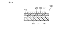
- FIG. 11A is a plan view showing a sixth modified example of a stretchable device according to the third embodiment of the present invention.
- FIG. 11B is a cross-sectional view showing a structure between A-A in FIG. 11A.
- Variation 6 is characterized in that, in a plan view, multiple first via portions 42I are located below a single first electrode portion 31I.
- the area of the connection region 43I can be made larger than when there is a single via portion. This can further improve the reliability of the interlayer connection.
- the required accuracy of alignment when joining the interlayer sheet 40I to the stretchable substrate 10I and the hurdle of the positional accuracy of the second stretchable wiring formed at a specified location on the interlayer sheet 40I can be reduced.
- FIG. 12A is a plan view showing a seventh modified example of a stretchable device according to the third embodiment of the present invention.
- FIG. 12B is a cross-sectional view showing a structure between A-A in FIG. 12A.
- FIG. 12A in consideration of ease of viewing the drawing, the arrangement and structure of the multiple internal elastic wirings located between the first elastic wiring 20J and the second elastic wiring 30J are mainly emphasized. In other words, the second elastic wiring is omitted from the illustration in FIG. 12A.
- Modification 7 is the same as modification 4 in that three or more elastic wires are arranged in the thickness direction of the elastic substrate 10J, but the internal elastic wires 70J, 80J located between the first elastic wire 20J and the second elastic wire 30J are located in multiple positions in the longitudinal extension direction of the interlayer sheet 40J.
- elastic wires 70J, 80J with a small area are arranged inside the device between two elastic wires 20J, 30J with a large area in the thickness direction of the elastic substrate 10J.
- These elastic wires 70J, 80J can be arranged in parallel at a predetermined interval on the interlayer sheet 40J.
- Some of the elastic wirings 70J are connected to the first elastic wiring 20J and the second elastic wiring 30J through the connection regions of the via portions. Meanwhile, the remaining elastic wirings 80J are not connected to the first elastic wiring 20J and the second elastic wiring 30J, and function as separate and independent wirings. In other words, the remaining elastic wirings 80J located inside function as elastic wirings that are not in contact with the first via portion 42J.
- first stretchable wiring and the second stretchable wiring make it possible for the first stretchable wiring and the second stretchable wiring to block noise that may invade the internal stretchable wiring.
- two or more types of wiring or wiring groups with different functions can be provided, which is advantageous in that the device functions can be enriched.
- Step 1 Fig. 13A is a plan view that illustrates step 1 of the method for producing a stretchable device according to the third embodiment of the present invention.
- a stretchable substrate 10 is prepared.
- Step 2 Fig. 13B is a plan view showing step 2 of the method for producing a stretchable device according to the third embodiment of the present invention.
- a wiring material is screen-printed on the stretchable substrate 10 and then dried. This allows the first stretchable wiring 20 to be formed on the stretchable substrate 10.
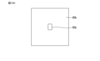
- Step 3 13C is a plan view showing step 3 of the method for producing a stretchable device according to the third embodiment of the present invention.
- a base material 40b to be used as an interlayer sheet is prepared.
- a laser is irradiated to the base material 40b to form a via hole 45b.
- Step 4 Fig. 13D is a plan view showing step 4 of the method for producing a stretchable device according to the third embodiment of the present invention.
- step 3 the base material 40b prepared in the same step is bonded to the stretchable base material 10 with the first stretchable wiring 20.
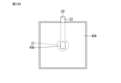
- Step 5 13E is a plan view showing step 5 of the method for producing a stretchable device according to the third embodiment of the present invention.
- step 4 similar to step 2, a wiring material is screen-printed using a squeegee at a predetermined location of the base material 40b as an interlayer sheet so as to be interlayer-connectable with the first electrode portion 21C of the first stretchable wiring 20C through the via hole 45b. Then, the wiring material is dried. As a result, the second stretchable wiring 30C can be formed on the obtained interlayer sheet 40.
- a part of the first via portion 42 forms a connection region 43, and the remaining part forms a non-connection region 44 that does not connect the first electrode portion 21C and the second electrode portion 31C.
- the wiring material is printed and applied so as not to cover or overlap the entire via hole in a plan view.
- the stretchable device may have the following features.
- ⁇ 3> The stretchable device according to ⁇ 1> or ⁇ 2>, wherein the first via portion further has, in addition to the connection region, a non-connection region that does not connect between the first electrode portion and the second electrode portion.
- ⁇ 4> The stretchable device according to ⁇ 3>, wherein the non-connected region of the first via portion is located outside the second electrode portion in a planar view.
- ⁇ 5> The stretchable device according to any one of ⁇ 1> to ⁇ 4>, wherein, in a planar view, the connection region occupies a part of the first via portion.
- the interlayer sheet further has at least one second via portion that entirely overlaps with the second electrode portion.
- the second via portion is the connection region.
- the interlayer sheet further has a third via portion that does not overlap the second electrode portion in a planar view.
- the interlayer sheet has a plurality of via portions regularly arranged at a predetermined interval in the sheet portion, and the plurality of via portions include the first via portion and the second via portion.
- the diameters of the plurality of via portions are smaller than the diameters of the first electrode portion and the second electrode portion.
- ⁇ 13> The stretchable device according to any one of ⁇ 3> to ⁇ 5>, wherein, in a planar view, the non-connected region of the first via portion extends from the second electrode portion toward an edge of the interlayer sheet.
- ⁇ 14> The stretchable device according to ⁇ 13>, wherein, in a plan view, the non-connected region of the first via portion continues from the second electrode portion to an edge of the interlayer sheet.
- ⁇ 15> The stretchable device according to ⁇ 13>, wherein an edge of the interlayer sheet is located inside an edge of the stretchable substrate in a plan view.
- ⁇ 16> In the thickness direction of the stretchable substrate, three or more of the stretchable wirings are arranged, and the electrode portion of one adjacent stretchable wiring and the electrode portion of the other adjacent stretchable wiring are connected to each other through the first via portion of the interlayer sheet.
- the stretchable device according to any one of ⁇ 1> to ⁇ 5>. ⁇ 17> When the three or more stretchable wirings are arranged, two or more of the first via portions are provided in which the non-connected regions are shifted in a planar view.
- the stretchable device according to ⁇ 16>. ⁇ 18> When the three or more stretchable wirings are arranged, the stretchable wiring does not contact the first via portion.
- a stretchable wiring having a small area is arranged between two stretchable wirings having a large area in the thickness direction of the stretchable substrate.
- ⁇ 20> The stretchable device according to ⁇ 19>, wherein the small area stretchable wirings are arranged in parallel at predetermined intervals on the interlayer sheet.
Landscapes
- Engineering & Computer Science (AREA)
- Microelectronics & Electronic Packaging (AREA)
- Manufacturing & Machinery (AREA)
- Structure Of Printed Boards (AREA)
Priority Applications (3)
| Application Number | Priority Date | Filing Date | Title |
|---|---|---|---|
| DE112024001499.2T DE112024001499T5 (de) | 2023-05-31 | 2024-05-24 | Flexible vorrichtung |
| JP2025524056A JP7835348B2 (ja) | 2023-05-31 | 2024-05-24 | 伸縮性デバイス |
| US19/371,039 US20260052628A1 (en) | 2023-05-31 | 2025-10-28 | Stretchable device |
Applications Claiming Priority (2)
| Application Number | Priority Date | Filing Date | Title |
|---|---|---|---|
| JP2023090216 | 2023-05-31 | ||
| JP2023-090216 | 2023-05-31 |
Related Child Applications (1)
| Application Number | Title | Priority Date | Filing Date |
|---|---|---|---|
| US19/371,039 Continuation US20260052628A1 (en) | 2023-05-31 | 2025-10-28 | Stretchable device |
Publications (1)
| Publication Number | Publication Date |
|---|---|
| WO2024247904A1 true WO2024247904A1 (ja) | 2024-12-05 |
Family
ID=93657546
Family Applications (1)
| Application Number | Title | Priority Date | Filing Date |
|---|---|---|---|
| PCT/JP2024/019140 Ceased WO2024247904A1 (ja) | 2023-05-31 | 2024-05-24 | 伸縮性デバイス |
Country Status (4)
| Country | Link |
|---|---|
| US (1) | US20260052628A1 (https=) |
| JP (1) | JP7835348B2 (https=) |
| DE (1) | DE112024001499T5 (https=) |
| WO (1) | WO2024247904A1 (https=) |
Citations (5)
| Publication number | Priority date | Publication date | Assignee | Title |
|---|---|---|---|---|
| JPH04336492A (ja) * | 1991-05-13 | 1992-11-24 | Nec Corp | 多層配線セラミック基板 |
| JPH0810792B2 (ja) * | 1991-05-10 | 1996-01-31 | 株式会社日立製作所 | 多層配線基板の製造方法 |
| JPH1154916A (ja) * | 1997-08-06 | 1999-02-26 | Noritake Co Ltd | 厚膜多層回路基板 |
| JP2002246752A (ja) * | 2001-02-19 | 2002-08-30 | Murata Mfg Co Ltd | セラミック多層基板のビアホール構造 |
| JP2021141370A (ja) * | 2020-03-02 | 2021-09-16 | 株式会社デンソー | 半導体パッケージ |
Family Cites Families (4)
| Publication number | Priority date | Publication date | Assignee | Title |
|---|---|---|---|---|
| JP2017113088A (ja) * | 2015-12-21 | 2017-06-29 | パナソニックIpマネジメント株式会社 | 生体センサー・デバイス |
| WO2018199084A1 (ja) * | 2017-04-28 | 2018-11-01 | 株式会社村田製作所 | 配線基板およびその製造方法 |
| JP7360089B2 (ja) | 2019-11-13 | 2023-10-12 | 株式会社オートネットワーク技術研究所 | 電池配線モジュール |
| JPWO2023042491A1 (https=) * | 2021-09-16 | 2023-03-23 |
-
2024
- 2024-05-24 DE DE112024001499.2T patent/DE112024001499T5/de active Pending
- 2024-05-24 WO PCT/JP2024/019140 patent/WO2024247904A1/ja not_active Ceased
- 2024-05-24 JP JP2025524056A patent/JP7835348B2/ja active Active
-
2025
- 2025-10-28 US US19/371,039 patent/US20260052628A1/en active Pending
Patent Citations (5)
| Publication number | Priority date | Publication date | Assignee | Title |
|---|---|---|---|---|
| JPH0810792B2 (ja) * | 1991-05-10 | 1996-01-31 | 株式会社日立製作所 | 多層配線基板の製造方法 |
| JPH04336492A (ja) * | 1991-05-13 | 1992-11-24 | Nec Corp | 多層配線セラミック基板 |
| JPH1154916A (ja) * | 1997-08-06 | 1999-02-26 | Noritake Co Ltd | 厚膜多層回路基板 |
| JP2002246752A (ja) * | 2001-02-19 | 2002-08-30 | Murata Mfg Co Ltd | セラミック多層基板のビアホール構造 |
| JP2021141370A (ja) * | 2020-03-02 | 2021-09-16 | 株式会社デンソー | 半導体パッケージ |
Also Published As
| Publication number | Publication date |
|---|---|
| DE112024001499T5 (de) | 2026-02-26 |
| JPWO2024247904A1 (https=) | 2024-12-05 |
| US20260052628A1 (en) | 2026-02-19 |
| JP7835348B2 (ja) | 2026-03-25 |
Similar Documents
| Publication | Publication Date | Title |
|---|---|---|
| US7025601B2 (en) | Interposer and method for making same | |
| JP3565835B1 (ja) | 配線基板およびその製造方法ならびに半導体装置およびその製造方法 | |
| JP2008153543A (ja) | 静電チャック | |
| JP6869209B2 (ja) | 配線基板 | |
| EP2333831B1 (en) | Method for packaging an electronic device | |
| TW200308188A (en) | Printed wiring board | |
| JP2004119871A (ja) | 多層プリント基板 | |
| WO2024247904A1 (ja) | 伸縮性デバイス | |
| CN119318210A (zh) | 伸缩性器件 | |
| US6369331B1 (en) | Printed circuit board for semiconductor package and method of making same | |
| US10517170B2 (en) | Multilayer substrate | |
| JP2001015643A5 (https=) | ||
| CN212461713U (zh) | 一种芯片柔性封装结构 | |
| JP7614487B2 (ja) | 半導体素子の転写方法 | |
| JP4925321B2 (ja) | 両面接続用配線板、両面接続用配線板の製造方法 | |
| CN217591205U (zh) | 一种防偏位多层软板结构 | |
| US20240422918A1 (en) | Stretchable device | |
| JP4436336B2 (ja) | 多数個取り配線基板およびその製造方法 | |
| JP7540611B2 (ja) | 伸縮デバイス | |
| JP5640861B2 (ja) | 電子部品の製造方法と配線基板 | |
| JP5556424B2 (ja) | 配線板および接続方法 | |
| WO2025192170A1 (ja) | 伸縮性デバイス | |
| WO2025033274A1 (ja) | 伸縮性デバイス | |
| JP2025153008A (ja) | 伸縮性を有する半導体装置 | |
| JP4640581B2 (ja) | カメラモジュールの実装構造 |
Legal Events
| Date | Code | Title | Description |
|---|---|---|---|
| 121 | Ep: the epo has been informed by wipo that ep was designated in this application |
Ref document number: 24815388 Country of ref document: EP Kind code of ref document: A1 |
|
| ENP | Entry into the national phase |
Ref document number: 2025524056 Country of ref document: JP Kind code of ref document: A |
|
| WWE | Wipo information: entry into national phase |
Ref document number: 2025524056 Country of ref document: JP |
|
| WWE | Wipo information: entry into national phase |
Ref document number: 112024001499 Country of ref document: DE |
|
| WWP | Wipo information: published in national office |
Ref document number: 112024001499 Country of ref document: DE |