WO2024228239A1 - 配線構造体を製造する方法 - Google Patents
配線構造体を製造する方法 Download PDFInfo
- Publication number
- WO2024228239A1 WO2024228239A1 PCT/JP2023/017056 JP2023017056W WO2024228239A1 WO 2024228239 A1 WO2024228239 A1 WO 2024228239A1 JP 2023017056 W JP2023017056 W JP 2023017056W WO 2024228239 A1 WO2024228239 A1 WO 2024228239A1
- Authority
- WO
- WIPO (PCT)
- Prior art keywords
- layer
- trench
- wiring
- seed
- substrate
- Prior art date
- Legal status (The legal status is an assumption and is not a legal conclusion. Google has not performed a legal analysis and makes no representation as to the accuracy of the status listed.)
- Ceased
Links
Images



Classifications
-
- H—ELECTRICITY
- H05—ELECTRIC TECHNIQUES NOT OTHERWISE PROVIDED FOR
- H05K—PRINTED CIRCUITS; CASINGS OR CONSTRUCTIONAL DETAILS OF ELECTRIC APPARATUS; MANUFACTURE OF ASSEMBLAGES OF ELECTRICAL COMPONENTS
- H05K3/00—Apparatus or processes for manufacturing printed circuits
- H05K3/02—Apparatus or processes for manufacturing printed circuits in which the conductive material is applied to the surface of the insulating support and is thereafter removed from such areas of the surface which are not intended for current conducting or shielding
- H05K3/04—Apparatus or processes for manufacturing printed circuits in which the conductive material is applied to the surface of the insulating support and is thereafter removed from such areas of the surface which are not intended for current conducting or shielding the conductive material being removed mechanically, e.g. by punching
-
- H—ELECTRICITY
- H05—ELECTRIC TECHNIQUES NOT OTHERWISE PROVIDED FOR
- H05K—PRINTED CIRCUITS; CASINGS OR CONSTRUCTIONAL DETAILS OF ELECTRIC APPARATUS; MANUFACTURE OF ASSEMBLAGES OF ELECTRICAL COMPONENTS
- H05K3/00—Apparatus or processes for manufacturing printed circuits
- H05K3/02—Apparatus or processes for manufacturing printed circuits in which the conductive material is applied to the surface of the insulating support and is thereafter removed from such areas of the surface which are not intended for current conducting or shielding
- H05K3/06—Apparatus or processes for manufacturing printed circuits in which the conductive material is applied to the surface of the insulating support and is thereafter removed from such areas of the surface which are not intended for current conducting or shielding the conductive material being removed chemically or electrolytically, e.g. by photo-etch process
-
- H—ELECTRICITY
- H05—ELECTRIC TECHNIQUES NOT OTHERWISE PROVIDED FOR
- H05K—PRINTED CIRCUITS; CASINGS OR CONSTRUCTIONAL DETAILS OF ELECTRIC APPARATUS; MANUFACTURE OF ASSEMBLAGES OF ELECTRICAL COMPONENTS
- H05K3/00—Apparatus or processes for manufacturing printed circuits
- H05K3/10—Apparatus or processes for manufacturing printed circuits in which conductive material is applied to the insulating support in such a manner as to form the desired conductive pattern
-
- H—ELECTRICITY
- H05—ELECTRIC TECHNIQUES NOT OTHERWISE PROVIDED FOR
- H05K—PRINTED CIRCUITS; CASINGS OR CONSTRUCTIONAL DETAILS OF ELECTRIC APPARATUS; MANUFACTURE OF ASSEMBLAGES OF ELECTRICAL COMPONENTS
- H05K3/00—Apparatus or processes for manufacturing printed circuits
- H05K3/10—Apparatus or processes for manufacturing printed circuits in which conductive material is applied to the insulating support in such a manner as to form the desired conductive pattern
- H05K3/18—Apparatus or processes for manufacturing printed circuits in which conductive material is applied to the insulating support in such a manner as to form the desired conductive pattern using precipitation techniques to apply the conductive material
Definitions
- This disclosure relates to a method for manufacturing a wiring structure having a wiring layer.
- a wiring structure including fine wiring such as a redistribution layer connected to the semiconductor element may be provided.
- the wiring structure may be formed by a semi-additive method including forming a resist layer having a pattern including an opening on a seed layer, forming an electrolytic plating layer on the seed layer in the opening, removing the resist layer, and removing unnecessary parts of the seed layer by etching (e.g., Patent Document 1).
- a trench method has been proposed in which an insulating layer constituting the wiring layer is formed from a photosensitive resin material, and an electrolytic plating layer is formed in the opening of the insulating layer patterned by exposure and development (e.g., Patent Document 2).
- This disclosure relates to a new method for manufacturing wiring structures having wiring layers containing fine wiring with high precision.
- the present disclosure includes the following. [1] Providing a resist layer on one major surface of a substrate; patterning the resist layer by exposure and development to thereby form a trench having a bottom surface including a surface of the substrate and a wall surface including a surface of the resist layer; forming a seed layer including an intra-trench seed portion continuously formed within the trench from a position on the bottom surface to a position on the wall surface, and an outer-trench seed portion provided on an opposite side of the resist layer from the substrate and continuously formed with the intra-trench seed portion; forming a metal plating layer on the seed layer, the metal plating layer including a filling plating portion that fills the trench together with the intra-trench seed portion and a portion provided on the outer-trench seed portion; removing a portion of the metal plating layer and the outer trench seed portion such that the resist layer is exposed and the filling plating portion remains; removing the resist layer from the main surface of the substrate so that wiring including the trench seed portion and the filling plating portion remains; A method for
- Wiring structures with wiring layers that include fine wiring can be manufactured with high precision.
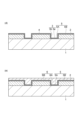
- 1A to 1C are process diagrams showing an example of a method for manufacturing a wiring structure.
- 1A to 1C are process diagrams showing an example of a method for manufacturing a wiring structure.
- 1A to 1C are process diagrams showing an example of a method for manufacturing a wiring structure.
- 4 is an electron microscope photograph of the intermediate structure after the trench and seed layer have been formed. 4 is an electron microscope photograph of the intermediate structure after a metal plating layer is formed. 1 is an electron microscope photograph of the formed wiring.
- the present invention is not limited to the following examples.
- FIGS. 1, 2, and 3 are process diagrams showing an example of a method for manufacturing a wiring structure having a wiring layer.
- the method shown in FIGS. 1 to 3 includes preparing a substrate 1, providing a resist layer 2 on one main surface 1S of the substrate 1, patterning the resist layer 2 by exposure and development to form a trench 3 in which the substrate 1 is exposed, forming a barrier layer 4 covering the substrate 1 and the resist layer 2, forming a seed layer 5 on the barrier layer 4, forming a metal plating layer 6 on the seed layer 5, removing a portion of the metal plating layer 6, the seed layer 5, and the barrier layer 4 to expose the resist layer 2, and removing the resist layer 2 from the main surface 1S of the substrate 1 so that wiring 11 including the seed layer 5 and the metal plating layer 6 remains.
- the substrate 1 may be a temporary support for forming a wiring structure, or may be a member including a circuit to which the wiring in the wiring structure is connected.
- the substrate 1 may be a member including a semiconductor element, and the wiring structure may be a rewiring layer to which the semiconductor element is connected.
- the method according to the present disclosure may be used to manufacture, for example, a fan-out type semiconductor package having a semiconductor element and a rewiring layer.
- the method according to the present disclosure may also be used to manufacture an interposer, which is a wiring structure that connects semiconductor elements together in so-called 2.5D, 2.3D, 2.1D, etc. semiconductor packages.
- the resist layer 2 can be formed from a resist material that is typically used for wiring formation, etc.
- the resist layer 2 may be provided on the main surface 1S by laminating a dry film resist.
- the resist layer 2 may be formed by a method that includes applying a liquid resist to the main surface 1S and drying the applied film.
- the resist material used to form resist layer 2 is removed after the metal plating layer for the wiring is formed, and is not used as a material for forming the insulating layer that constitutes the wiring layer. Therefore, the resist material can be selected mainly based on its performance as a photosensitive material, without having to consider its performance as an insulating layer.
- the resist layer 2 can be patterned by a normal method including exposure and subsequent development to form a trench 3 exposing the substrate 1.
- the trench 3 has a bottom surface 3a including the surface (main surface 1S) of the substrate 1 and a wall surface 3b including the surface (side surface) of the resist layer 2, and extends in the in-plane direction of the main surface 1S of the substrate 1.
- the trench 3 includes a portion corresponding to the position where the wiring is to be formed.
- a plurality of trenches 3 may be independently provided on the main surface 1S.
- the minimum width of the trench 3 may be, for example, 0.5 ⁇ m or more and 10 ⁇ m or less.
- the minimum distance between the trenches 3 may be, for example, 0.5 ⁇ m or more and 10 ⁇ m or less.
- the depth of the trench 3 (or the thickness of the resist layer 2) may be, for example, 1 ⁇ m or more and 15 ⁇ m or less.
- the minimum width of the trench 3 can be the minimum value of the width in a direction perpendicular to the longitudinal direction of the trench 3.
- the barrier layer 4 includes a portion formed continuously from a position on the bottom surface 3a to a position on the wall surface 3b in the trench 3, and a portion provided on the surface of the resist layer 2 opposite the substrate 1.
- the barrier layer 4 forms a trench or a recess having a shape corresponding to the trench 3.
- the barrier layer 4 is a layer provided mainly to suppress migration from the wiring, and is interposed between the wiring 11 to be formed and the substrate 1 and the resist layer 2.
- the barrier layer 4 may be, for example, a layer containing titanium.
- the thickness of the barrier layer 4 may be, for example, 10 nm or more and 50 nm or less.
- the barrier layer 4 may be formed by, for example, a sputtering method. The barrier layer 4 does not have to be provided.
- the seed layer 5 formed on the barrier layer 4 includes an intra-trench seed portion 5A formed continuously from a position on the bottom surface 3a to a position on the wall surface 3b in the trench 3, and an outer-trench seed portion 5B provided on the opposite side of the resist layer 2 to the substrate 1.
- the outer-trench seed portion 5B is formed continuously with the intra-trench seed portion 5A.
- the seed layer 5 is used to form the metal plating layer 6 by electrolytic plating.
- the seed layer 5 can be a layer containing a metal such as copper.
- the thickness of the seed layer may be, for example, 50 nm to 500 nm.
- the seed layer 5 can be formed by, for example, a sputtering method.
- the seed layer 5 may be formed by electroless plating.
- a metal plating layer 6 is formed on the seed layer 5 by electrolytic plating.
- the metal plating layer 6 includes a filling plating portion 6A that fills the trench 3 together with the trench-inside seed portion 5A and the barrier layer 4 of the seed layer 5, and a portion provided on the trench-outside seed portion 5B of the seed layer 5.
- the metal plating layer 6 is usually formed so as to cover the entire surface of the seed layer 5 opposite the substrate 1.
- the metal plating layer 6 can be a layer containing copper.
- the surface of the metal plating layer 6 opposite the substrate 1 can be flat or can have irregularities.
- the thickness of the filling plating portion 6A of the metal plating layer 6 (thickness in the thickness direction of the substrate 1) can be 1 ⁇ m or more and 15 ⁇ m or less.
- the thickness of the portion of the metal plating layer 6 provided on the trench-outside seed portion 5B can be 0.1 ⁇ m or more and 5 ⁇ m or less.
- the metal plating layer 6 is formed, as shown in FIG. 3(f), a portion of the metal plating layer 6, the outer trench seed portion 5B of the seed layer 5, and a portion of the barrier layer 4 are removed so that the resist layer 2 is exposed and the filling plating portion 6A remains.
- the metal plating layer 6, the seed layer 5, and the barrier layer 4 can be removed by, for example, etching or chemical mechanical polishing (CMP). As a result of the removal, a flat surface including the surface of the resist layer 2 and the surface of the remaining filling plating portion 6A may be formed.
- the resist layer 2 is removed from the main surface 1S of the substrate 1 so as to leave the wiring 11 including the trench seed portion 5A and the filling plating portion 6A.
- the barrier layer 4 including the portion covering the side surface of the wiring 11 is also left behind along with the wiring 11.
- the resist layer 2 can be removed, for example, by dissolving it in a stripping solution.
- an insulating layer 21 may be formed on the main surface 1S of the substrate 1 to surround the wiring 11, as shown in FIG. 4(h). This forms a wiring layer 31 including the wiring 11 and the insulating layer 21.
- the insulating layer 21 may be an insulating resin layer.
- the insulating layer 21 may include polybenzoxazole, polyimide, or a combination thereof.
- a part or the entirety of the main surface 1S of the substrate 1 may be the surface of an insulating layer similar to the insulating layer 21.
- an additional wiring layer 32 including an additional wiring 12 and an additional insulating layer 22 surrounding the additional wiring 12 may be further laminated on the surface of the wiring layer 31 opposite the substrate 1.
- the additional wiring 12 may be formed in the same manner as the wiring 11, in which case the additional wiring 12 may also include an in-trench seed portion 5A of the seed layer 5 and a filling plating portion 6A of the metal plating layer 6.
- the additional insulating layer 22 may be a layer similar to the insulating layer 21.
- a liquid resist was applied onto the main surface of a substrate having a surface containing polyimide resin, and the coating was dried to form a resist layer.
- the resist layer was patterned by exposure to ultraviolet light and subsequent development to form multiple linear trenches extending across the main surface of the substrate.
- the trenches had a bottom surface that included the surface of the substrate and wall surfaces that included the surface of the resist layer.
- the maximum width of each trench and the distance between adjacent trenches were approximately 5 ⁇ m.
- FIG. 5 is an electron microscope photograph of the intermediate structure after the trench and seed layer were formed.
- the photograph in Figure 5(b) includes a cross section perpendicular to the longitudinal direction of the trench.
- the seed layer formed had an in-trench seed portion formed continuously from the bottom surface to the wall surfaces within the trench, and an outside-trench seed portion formed continuously with the in-trench seed portion on the side of the resist layer opposite the substrate.
- FIG. 6 is an electron microscope photograph of an intermediate structure including the metal plating layer.
- the photograph in Figure 6(b) includes a cross section perpendicular to the longitudinal direction of the trench.
- the metal plating layer had a filling plating portion that filled the trench together with the seed portion inside the trench, and a portion provided on the seed portion outside the trench.
- FIG. 7 is an electron microscope photograph of the wiring layer including the metal plating layer (filled plating portion) remaining on the substrate. It was confirmed that wiring with a good shape was formed with high precision. Wiring was formed using the same procedure as above, except that the maximum width of each trench and the spacing between adjacent trenches were changed to approximately 3 ⁇ m or approximately 2 ⁇ m. In both cases, wiring with a good shape was formed with high precision.
Landscapes
- Engineering & Computer Science (AREA)
- Manufacturing & Machinery (AREA)
- Microelectronics & Electronic Packaging (AREA)
- Internal Circuitry In Semiconductor Integrated Circuit Devices (AREA)
Abstract
Description
[1]
基板の一方の主面上にレジスト層を設けることと、
前記レジスト層を露光及び現像によってパターニングし、それにより前記基板の表面を含む底面と前記レジスト層の表面を含む壁面とを有するトレンチを形成することと、
前記トレンチ内で前記底面上の位置から前記壁面上の位置にかけて連続的に形成されたトレンチ内シード部と前記レジスト層の前記基板とは反対側に設けられ前記トレンチ内シード部と連続的に形成されたトレンチ外シード部とを含む、シード層を形成することと、
前記シード層上に、前記トレンチ内シード部とともに前記トレンチを充填する充填めっき部と前記トレンチ外シード部上に設けられた部分とを含む、金属めっき層を形成することと、
前記金属めっき層の一部、及び前記トレンチ外シード部を、前記レジスト層が露出するとともに前記充填めっき部が残るように除去することと、
前記トレンチ内シード部及び前記充填めっき部を含む配線が残るように、前記レジスト層を前記基板の前記主面上から除去することと、
を含む、配線構造体を製造する方法。
[2]
当該方法が、前記トレンチ内で前記底面上の位置から前記壁面上の位置にかけて連続的に形成された部分を含むバリア層を形成することを更に含み、
前記バリア層上に前記シード層が形成され、
前記配線とともに前記バリア層が残るように、前記レジスト層が前記基板の前記主面上から除去される、
[1]に記載の方法。
[3]
当該方法が、前記基板の前記主面上で前記配線を囲む絶縁層を形成し、それにより前記配線及び前記絶縁層を含む配線層を形成することを更に含む、[1]又は[2]に記載の方法。
[4]
当該方法が、前記配線層の前記基板とは反対側の表面上に、追加の配線、及び前記追加の配線を囲む追加の絶縁層を含む、1層以上の追加の配線層を積層することを更に含む、[3]に記載の方法。
Claims (4)
- 基板の一方の主面上にレジスト層を設けることと、
前記レジスト層を露光及び現像によってパターニングし、それにより前記基板の表面を含む底面と前記レジスト層の表面を含む壁面とを有するトレンチを形成することと、
前記トレンチ内で前記底面上の位置から前記壁面上の位置にかけて連続的に形成されたトレンチ内シード部と前記レジスト層の前記基板とは反対側に設けられ前記トレンチ内シード部と連続的に形成されたトレンチ外シード部とを含む、シード層を形成することと、
前記シード層上に、前記トレンチ内シード部とともに前記トレンチを充填する充填めっき部と前記トレンチ外シード部上に設けられた部分とを含む、金属めっき層を形成することと、
前記金属めっき層の一部、及び前記トレンチ外シード部を、前記レジスト層が露出するとともに前記充填めっき部が残るように除去することと、
前記トレンチ内シード部及び前記充填めっき部を含む配線が残るように、前記レジスト層を前記基板の前記主面上から除去することと、
を含む、配線構造体を製造する方法。 - 当該方法が、前記トレンチ内で前記底面上の位置から前記壁面上の位置にかけて連続的に形成された部分を含むバリア層を形成することを更に含み、
前記バリア層上に前記シード層が形成され、
前記配線とともに前記バリア層が残るように、前記レジスト層が前記基板の前記主面上から除去される、
請求項1に記載の方法。 - 当該方法が、前記基板の前記主面上で前記配線を囲む絶縁層を形成し、それにより前記配線及び前記絶縁層を含む配線層を形成することを更に含む、請求項1に記載の方法。
- 当該方法が、前記配線層の前記基板とは反対側の表面上に、追加の配線、及び前記追加の配線を囲む追加の絶縁層を含む、1層以上の追加の配線層を積層することを更に含む、請求項3に記載の方法。
Priority Applications (4)
| Application Number | Priority Date | Filing Date | Title |
|---|---|---|---|
| PCT/JP2023/017056 WO2024228239A1 (ja) | 2023-05-01 | 2023-05-01 | 配線構造体を製造する方法 |
| JP2025518065A JPWO2024228239A1 (ja) | 2023-05-01 | 2023-05-01 | |
| CN202380034681.0A CN119256631A (zh) | 2023-05-01 | 2023-05-01 | 制造配线结构体的方法 |
| KR1020257034090A KR20260002682A (ko) | 2023-05-01 | 2023-05-01 | 배선 구조체를 제조하는 방법 |
Applications Claiming Priority (1)
| Application Number | Priority Date | Filing Date | Title |
|---|---|---|---|
| PCT/JP2023/017056 WO2024228239A1 (ja) | 2023-05-01 | 2023-05-01 | 配線構造体を製造する方法 |
Publications (1)
| Publication Number | Publication Date |
|---|---|
| WO2024228239A1 true WO2024228239A1 (ja) | 2024-11-07 |
Family
ID=93332930
Family Applications (1)
| Application Number | Title | Priority Date | Filing Date |
|---|---|---|---|
| PCT/JP2023/017056 Ceased WO2024228239A1 (ja) | 2023-05-01 | 2023-05-01 | 配線構造体を製造する方法 |
Country Status (4)
| Country | Link |
|---|---|
| JP (1) | JPWO2024228239A1 (ja) |
| KR (1) | KR20260002682A (ja) |
| CN (1) | CN119256631A (ja) |
| WO (1) | WO2024228239A1 (ja) |
Citations (4)
| Publication number | Priority date | Publication date | Assignee | Title |
|---|---|---|---|---|
| JP2017092308A (ja) * | 2015-11-12 | 2017-05-25 | 富士通株式会社 | 配線の形成方法および配線構造 |
| US20200075496A1 (en) * | 2018-08-28 | 2020-03-05 | Taiwan Semiconductor Manufacturing Co., Ltd. | Package and method of fabricating the same |
| JP2022138469A (ja) * | 2021-03-10 | 2022-09-26 | 凸版印刷株式会社 | 多層配線基板及びその製造方法 |
| JP2022170150A (ja) * | 2021-04-28 | 2022-11-10 | 凸版印刷株式会社 | 多層配線基板、複合配線基板、パッケージ化デバイス、及び多層配線基板の製造方法 |
Family Cites Families (2)
| Publication number | Priority date | Publication date | Assignee | Title |
|---|---|---|---|---|
| JP4269746B2 (ja) | 2002-04-02 | 2009-05-27 | 凸版印刷株式会社 | プリント配線板の製造方法、プリント配線板および半導体パッケージ |
| JP2018085358A (ja) | 2016-11-21 | 2018-05-31 | 日立化成株式会社 | 半導体装置の製造方法 |
-
2023
- 2023-05-01 KR KR1020257034090A patent/KR20260002682A/ko active Pending
- 2023-05-01 WO PCT/JP2023/017056 patent/WO2024228239A1/ja not_active Ceased
- 2023-05-01 JP JP2025518065A patent/JPWO2024228239A1/ja active Pending
- 2023-05-01 CN CN202380034681.0A patent/CN119256631A/zh active Pending
Patent Citations (4)
| Publication number | Priority date | Publication date | Assignee | Title |
|---|---|---|---|---|
| JP2017092308A (ja) * | 2015-11-12 | 2017-05-25 | 富士通株式会社 | 配線の形成方法および配線構造 |
| US20200075496A1 (en) * | 2018-08-28 | 2020-03-05 | Taiwan Semiconductor Manufacturing Co., Ltd. | Package and method of fabricating the same |
| JP2022138469A (ja) * | 2021-03-10 | 2022-09-26 | 凸版印刷株式会社 | 多層配線基板及びその製造方法 |
| JP2022170150A (ja) * | 2021-04-28 | 2022-11-10 | 凸版印刷株式会社 | 多層配線基板、複合配線基板、パッケージ化デバイス、及び多層配線基板の製造方法 |
Also Published As
| Publication number | Publication date |
|---|---|
| CN119256631A (zh) | 2025-01-03 |
| KR20260002682A (ko) | 2026-01-06 |
| JPWO2024228239A1 (ja) | 2024-11-07 |
Similar Documents
| Publication | Publication Date | Title |
|---|---|---|
| KR102116060B1 (ko) | 반도체 장치 및 그 제조방법 | |
| JP4250154B2 (ja) | 半導体チップ及びその製造方法 | |
| US20080283277A1 (en) | Wiring board manufacturing method and wiring board | |
| Hu et al. | 2/2um Embedded Fine Line Technology for Organics Interposer Applications | |
| JPH10209273A (ja) | 半導体装置の製造方法 | |
| KR20010088866A (ko) | 고밀도 내부연결 인쇄 배선기판의 응력 완화 방법에 따른퇴적된 박막 축적 층의 디멘션화를 위한 배선기판 형성방법 및 그 배선기판 | |
| CN111867232A (zh) | 线路载板结构及其制作方法与芯片封装结构 | |
| TWI607678B (zh) | 中介層結構及其製作方法 | |
| KR20260002682A (ko) | 배선 구조체를 제조하는 방법 | |
| US10897823B2 (en) | Circuit board, package structure and method of manufacturing the same | |
| TWI613781B (zh) | 中介層結構及其製造方法 | |
| JP2008085373A (ja) | プリント配線板およびその製造方法 | |
| TWI765647B (zh) | 封裝載板及其製作方法 | |
| CN1306574C (zh) | 导电通孔制作工艺 | |
| KR100763760B1 (ko) | 반도체 소자 제조 방법 | |
| CN119626905B (zh) | 一种封装基板结构及其制备方法 | |
| KR100440472B1 (ko) | 반도체 소자 제조 방법 | |
| TWI598014B (zh) | 電路板結構與其製造方法 | |
| JPWO2024262629A5 (ja) | ||
| KR20190035193A (ko) | 미세 패턴의 회로기판 제조방법 | |
| TW202505974A (zh) | 在半導體裝置中形成abf插塞元件的方法、半導體基板的被動裝置及半導體裝置 | |
| CN109585359B (zh) | 半导体结构及其形成方法 | |
| CN118234144A (zh) | 将裸片嵌入载体层合材料中的方法 | |
| US9570342B1 (en) | Via structure and method for its fabrication | |
| KR100770449B1 (ko) | 반도체 소자의 비아 형성방법 |
Legal Events
| Date | Code | Title | Description |
|---|---|---|---|
| WWE | Wipo information: entry into national phase |
Ref document number: 202380034681.0 Country of ref document: CN Ref document number: 18857453 Country of ref document: US |
|
| 121 | Ep: the epo has been informed by wipo that ep was designated in this application |
Ref document number: 23935753 Country of ref document: EP Kind code of ref document: A1 |
|
| WWP | Wipo information: published in national office |
Ref document number: 202380034681.0 Country of ref document: CN |
|
| ENP | Entry into the national phase |
Ref document number: 2025518065 Country of ref document: JP Kind code of ref document: A |
|
| WWE | Wipo information: entry into national phase |
Ref document number: 2025518065 Country of ref document: JP |
|
| NENP | Non-entry into the national phase |
Ref country code: DE |
|
| 122 | Ep: pct application non-entry in european phase |
Ref document number: 23935753 Country of ref document: EP Kind code of ref document: A1 |