WO2024225388A1 - 伸縮性デバイス - Google Patents
伸縮性デバイス Download PDFInfo
- Publication number
- WO2024225388A1 WO2024225388A1 PCT/JP2024/016278 JP2024016278W WO2024225388A1 WO 2024225388 A1 WO2024225388 A1 WO 2024225388A1 JP 2024016278 W JP2024016278 W JP 2024016278W WO 2024225388 A1 WO2024225388 A1 WO 2024225388A1
- Authority
- WO
- WIPO (PCT)
- Prior art keywords
- stretchable
- wiring
- substrate
- region
- electronic component
- Prior art date
- Legal status (The legal status is an assumption and is not a legal conclusion. Google has not performed a legal analysis and makes no representation as to the accuracy of the status listed.)
- Ceased
Links
Images


Classifications
-
- H—ELECTRICITY
- H05—ELECTRIC TECHNIQUES NOT OTHERWISE PROVIDED FOR
- H05K—PRINTED CIRCUITS; CASINGS OR CONSTRUCTIONAL DETAILS OF ELECTRIC APPARATUS; MANUFACTURE OF ASSEMBLAGES OF ELECTRICAL COMPONENTS
- H05K1/00—Printed circuits
- H05K1/02—Details
Definitions
- the present invention relates to a stretchable device.
- a stretchable device has been known that includes a stretchable substrate, stretchable wiring provided on one main surface of the stretchable substrate, an electronic component mounted so as to be electrically connectable to the stretchable wiring, and an adhesive layer provided on the other main surface of the stretchable substrate.
- the inventors of the present application have found that the following points need to be improved in conventional stretchable devices. Specifically, while the stretchable substrate and stretchable wiring are stretchable, the mounted electronic components are non-stretchable. Therefore, there is a risk that it may be difficult to ensure the mounting reliability of non-stretchable electronic components due to the stress that occurs when the stretchable substrate etc. stretches.
- the present invention aims to provide a stretchable device that can optimally ensure the mounting reliability of electronic components even when stretched.
- the present invention comprises a stretchable substrate, a stretchable wiring provided on one main surface of the stretchable substrate, an electronic component provided so as to be electrically connectable to the stretchable wiring, and an adhesive layer provided on the other main surface of the stretchable substrate, A stretchable device is provided, wherein at least one of the stretchable substrate and the adhesive layer has discontinuous regions.
- the stretchable device according to one embodiment of the present invention can ensure the mounting reliability of electronic components even when stretched.
- FIG. 1A is a plan view illustrating a stretchable device according to a first embodiment of the present invention.
- FIG. 1B is a schematic cross-sectional view taken along line II of FIG. 1A.
- FIG. 2A is a plan view that illustrates a first step of producing a stretchable device according to a first embodiment of the present invention.
- FIG. 2B is a schematic cross-sectional view taken along line II-II of FIG. 2A.
- FIG. 2C is a plan view that illustrates a second step of producing a stretchable device according to the first embodiment of the present invention.
- FIG. 2D is a schematic cross-sectional view taken along line III-III in FIG. 2C.
- FIG. 5 is a plan view illustrating a stretchable device according to a fourth embodiment of the present invention.
- FIG. 6A is a plan view illustrating a stretchable device according to a fifth embodiment of the present invention.
- FIG. 6B is a schematic cross-sectional view taken along line VIB-VIB of FIG. 6A.
- FIG. 7A is a plan view illustrating a stretchable device according to a fifth embodiment of the present invention.
- FIG. 7B is a schematic cross-sectional view taken along line VIIB-VIIB of FIG. 7A.
- FIG. 8 is a schematic cross-sectional view showing a modification of FIG. 7B.
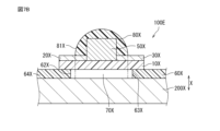
- FIG. 1A is a plan view showing a stretchable device according to a first embodiment of the present invention.
- FIG. 1B is a schematic cross-sectional view taken along line I-I in FIG. 1A.
- the stretchable device 100 comprises a stretchable substrate 10, a first stretchable wiring 20 and a second stretchable wiring 30 disposed on one main surface of the stretchable substrate 10 and spaced apart from the first stretchable wiring 20, and an electronic component 50 mounted so as to be electrically connectable to the first stretchable wiring 20 and the second stretchable wiring 30 via solder 40 (see Figs. 1A and 1B).
- the stretchable device 100 may also have an adhesive layer on the other main surface of the stretchable substrate 10.
- the stretchable substrate 10 is a sheet-like or film-like stretchable substrate, and is made of, for example, a resin material having stretchability.
- resin materials for the stretchable substrate 10 include thermoplastic polyurethane (TPU), polyethylene (PE), polystyrene (PS), polyethylene terephthalate (PET), etc.
- the thickness of the stretchable substrate 10 is not particularly limited, but is preferably 100 ⁇ m or less, and more preferably 50 ⁇ m or less, from the viewpoint of not inhibiting the stretching of the surface of the living body when attached to the living body.
- the thickness of the stretchable substrate 1 is preferably 20 ⁇ m or more from the viewpoint of ensuring a certain strength.
- the first elastic wiring 20 and the second elastic wiring 30 are provided on the elastic substrate 10, specifically on its main surface.
- above includes a state where it is located above an element and separated from it, i.e., above an element via another object, a state where it is located above an element with a gap, and a state where it is located directly above an element and in contact with it.
- the first elastic wiring 20 and the second elastic wiring 30 arranged on the elastic substrate 10 includes the first and second elastic wiring 20, 30 in contact with the main surface of the elastic substrate 10, and the first and second elastic wiring 20, 30 in a state where they are separated from the main surface via another member (for example, a resin layer described below) without directly contacting the main surface of the elastic substrate 10.
- another member for example, a resin layer described below
- the resin layer may be formed of at least one resin material selected from the group consisting of polyimide-based, epoxy-based, urethane-based, and acrylic-based resins.
- the resin layer may also be formed of an inorganic material such as alumina or silicon dioxide.
- the first elastic wiring 20 and the second elastic wiring 30 each have a connection portion 21, 31 that can be electrically connected to the electronic component 50, and an extension portion 22, 32 (which may also be called an extension portion) that is continuous with each connection portion 21, 31.
- the longitudinal direction of the extension portions 22, 32 of the elastic wirings 20, 30 extends in one direction.
- the "connection portion" refers to the area that overlaps with the electronic component when viewed from the thickness direction of the elastic substrate.
- the first elastic wiring 20 and the second elastic wiring 30 each contain conductive particles and a resin.
- each elastic wiring may be a mixture of metal powder such as Ag, Cu, Ni, etc. as conductive particles and an elastomer resin such as a silicone resin.
- the average particle size of the conductive particles is not particularly limited, but is preferably 0.01 ⁇ m or more and 10 ⁇ m or less.
- the conductive particles are preferably spherical in shape.
- each elastic wire is not particularly limited, but is preferably 100 ⁇ m or less, and more preferably 50 ⁇ m or less.
- the thickness of each elastic wire is preferably 0.01 ⁇ m or more.
- the line width of each elastic wire is not particularly limited, but is preferably 0.1 ⁇ m or more, and more preferably 1 mm or less.
- the shape, etc. of each elastic wire is not particularly limited.
- the extension direction of the first stretchable wiring 20 and the second stretchable wiring 30 is the longitudinal direction of the stretchable device 100 (i.e., the stretching direction).
- the electronic component 50 is disposed at a distance from the stretchable substrate 10 in the thickness direction X of the stretchable substrate 10.
- the electronic component 50 is not particularly limited, but examples thereof include a thermistor, a chip capacitor, and a chip coil.
- the electronic component 50 has a main body 51 and a first electrode portion 52 and a second electrode portion 53 that are provided on the main body 51 and face each other.
- the first electrode portion 52 is electrically connected to the connection portion 21 of the first stretchable wiring 20 via the solder 40.
- the second electrode portion 53 is electrically connected to the connection portion 31 of the second stretchable wiring 30.
- the main body 51 of the electronic component 50 is non-stretchable.
- the adhesive layer also has adhesiveness that allows the stretchable device 100 to be attached to an adherend such as a living body.
- the adhesive layer can be positioned between the stretchable substrate 10 and the adherend such as a living body.
- the adhesive layer has a first main surface facing the adherend, such as a living body, and a second main surface on the opposite side.
- the first adhesive layer preferably has adhesiveness on both main surfaces.
- the first main surface of the adhesive layer can be attached to a living body, etc.
- the second main surface of the adhesive layer can be attached to the stretchable substrate 10.
- a protective layer may further be disposed between the second main surface of the adhesive layer and the stretchable substrate 10 from the viewpoint of improving waterproofing, etc.
- the adhesive layer there are no particular restrictions on the adhesive layer, so long as it is an adhesive that is mild to the skin, has sufficient pressure-sensitive adhesive properties, and can be easily peeled off from the skin after use.
- the adhesive layer may be made of a pressure-sensitive adhesive or the like, although it is not particularly limited.
- the pressure-sensitive adhesive there is no particular limit to the pressure-sensitive adhesive, so long as it is one that can be laminated on the stretchable substrate 10 and generally used.
- rubber-, acrylic-, or silicone-based pressure-sensitive adhesives can be used.
- a pressure-sensitive adhesive When a pressure-sensitive adhesive is used, it can be bonded to the opposing member (stretchable substrate) at a relatively low temperature, so that deterioration or distortion of the stretchable substrate 10 can be prevented by using excessive heat or UV energy.
- the inventors of the present application conducted extensive research into solutions for achieving stress relaxation between the elastic wiring 20, 30 and the mounted electronic component 50 during expansion and contraction, and as a result came up with the idea of using an elastic substrate 10 having a different configuration from conventional ones.
- the first embodiment is characterized in that, as viewed from the thickness direction X of the stretchable substrate, at least the stretchable substrate 10 has a discontinuous region 11 arranged around the connection portions 21, 31.
- the longitudinal portion can extend at least along a direction parallel to the extension direction of the extension portions 21, 31 of the stretchable wiring 20, 30.
- the "parallel direction” here is not limited to a completely parallel direction, but means a completely parallel direction or a substantially or approximately parallel direction.
- the longitudinal portion of the discontinuous region 11 can extend along the longitudinal direction of the extension portions 21, 31 of the stretchable wiring 20, 30. That is, the longitudinal portion of the discontinuous region 11 can extend along the longitudinal direction of the stretchable wiring 20, 30.
- discontinuous region 11 arranged around connection parts 21, 31 of elastic wiring 20, 30 refers to a discontinuous region 11 arranged at a location where the shortest distance between the discontinuous region 11 and the connection part of the elastic wiring is 5% to 50% of the shortest distance between the outer edge of the elastic substrate and the connection part.
- discontinuous region 11 arranged around connection parts 21, 31 of elastic wiring 20, 30 refers to a discontinuous region 11 arranged at a location where the shortest distance between the discontinuous region 11 and the connection part can be less than twice the shortest distance between the discontinuous region 11 and the main body part 51.
- This feature makes it possible to prevent the stretching force caused by the stretching of the stretchable substrate 10 from acting at the discontinuous regions 11. That is, in this embodiment, the discontinuous regions 11 are positioned so as to mitigate the stretching force of the stretchable substrate 10 acting in a predetermined direction.
- the discontinuous regions 11 may be through holes that penetrate from one main surface of the elastic substrate 10 to the other main surface.
- the discontinuous regions 11 may also be in the form of grooves. If in the form of grooves, the discontinuous regions 11 may be 50% to 99%, preferably 60% to 99%, more preferably 70% to 99%, and even more preferably 80% to 99% of the thickness of the elastic substrate 10.
- the ratio of depth to width of the discontinuous region 11 may be 1:2.
- the discontinuous region 11 may have a depth of 50 ⁇ m or more and a width of 100 ⁇ m or more. It is preferable that the width of the discontinuous region 11 is at least twice the depth.
- the extension portions 22, 32 of the elastic wiring 20, 30 extend in one direction, and in a planar view, the discontinuous region 11 is disposed on at least one side of the electronic component 50.
- the discontinuous region 11 can be disposed on both sides of the electronic component 50. That is, the discontinuous region 11 can be disposed in a direction intersecting the extension direction of the extension portions 22, 32 of the elastic wiring 20, 30.
- the method for producing the stretchable device 100 of the first embodiment is described below.
- FIG. 2A is a plan view showing a first step of producing a stretchable device according to a first embodiment of the present invention
- Fig. 2B is a schematic cross-sectional view taken along line II-II in Fig. 2A.
- an elastic substrate 10 is prepared.
- This elastic substrate 10 is cut while taking into consideration the size, shape, and mounting location of the first and second elastic wiring to be arranged later and the electronic components to be mounted.
- a Pinnacle (registered trademark) blade can be used for the cutting process.
- discontinuous regions 11 whose longitudinal portions extend in the longitudinal direction of the stretchable substrate 10 and whose transverse portions are continuous with the longitudinal portions and extend in the transverse direction of the stretchable substrate 10.
- two sets of discontinuous regions 11 that face each other at a distance in the transverse direction of the stretchable substrate 10 are prepared in the longitudinal direction of the stretchable substrate 10, forming a total of four discontinuous regions 11.
- FIG. 2C is a plan view diagrammatically illustrating a second manufacturing step of the stretchable device according to the first embodiment of the present invention
- Fig. 2D is a diagrammatic cross-sectional view diagrammatically illustrating the section between III-III in Fig. 2C.
- the first and second elastic wirings 20, 30 are prepared so that a portion that will later become a connection portion that can be electrically connected to an electronic component is located between two discontinuous regions 11 that are spaced apart from each other in the short side direction of the elastic substrate 10.
- These elastic wirings 20, 30 can be formed by screen printing the wiring material, and then drying it at about 100°C for a predetermined time in a drying process.
- FIG. 2E is a plan view diagrammatically illustrating a third step of producing a stretchable device according to a first embodiment of the present invention
- Fig. 2F is a diagrammatic cross-sectional view diagrammatically illustrating a section between IV-IV in Fig. 2E.
- solder paste 40 ⁇ is positioned on the portions that will later become connection portions that can be electrically connected to electronic components.
- a silver-based paste can be used as the solder paste.
- FIG. 2G is a plan view diagrammatically illustrating a fourth step of fabricating a stretchable device according to a first embodiment of the present invention
- Fig. 2H is a diagrammatic cross-sectional view diagrammatically illustrating the stretchable device according to the first embodiment of the present invention, taken along line VV in Fig. 2G.
- the first electrode portion 52 and the second electrode portion 53 of the electronic component 50 are positioned on each solder paste, and then soldering is performed in a reflow furnace for a predetermined time (e.g., 60 to 300 seconds) through the processes of preheating, main heating, and cooling.
- a predetermined time e.g. 60 to 300 seconds
- the temperature is raised while volatilizing the solvent contained in the solder paste, and is maintained at a constant temperature that easily activates the flux.
- the temperature of the substrate and electronic component is raised evenly until it reaches a temperature at which the solder melts.
- Fig. 3 is a plan view diagrammatically illustrating the stretchable device according to the second embodiment of the present invention.
- the second embodiment differs from the first embodiment in that the discontinuous region 11A formed in the stretchable substrate 10A is continuous from the periphery of the connection portion of the first stretchable wiring 20 to the periphery of the connection portion of the second stretchable wiring 30.
- the stretching force of the stretchable substrate 10A acting in a predetermined direction can be more suitably alleviated in the discontinuous region 11A compared to the case of embodiment 1.
- the action of the stretching force on the non-stretchable electronic component 50 (the main body part 51) mounted on the stretchable substrate 10 can be more suitably suppressed.
- the stress that may occur between the stretchable wirings 20, 30 arranged on the stretchable substrate 10A and the electronic component 50 when the device 100A stretches can be more suitably alleviated.
- Fig. 4 is a plan view diagrammatically illustrating a stretchable device according to the third embodiment of the present invention.
- the third embodiment differs from the first embodiment in that, in a plan view, the discontinuous region 11B formed in the stretchable substrate 10B is arranged to completely surround the outer edge of the connection between the first stretchable wiring 20 and the second stretchable wiring 30, except for the installation location of the stretchable wiring.
- the surrounding form of the discontinuous region 11B allows the expansion and contraction force of the stretchable substrate 10B acting in a predetermined direction to be more suitably alleviated in the discontinuous region 11B than in the case of embodiment 1.
- This allows the action of the expansion and contraction force on the non-stretchable electronic component 50 (the main body 51) mounted on the stretchable substrate 10 to be more suitably suppressed than in the discontinuous region 11 of embodiment 1.
- it is possible to more suitably alleviate stress that may occur between the stretchable wiring 20, 30 arranged on the stretchable substrate 10B and the electronic component 50 when the device 100B expands and contracts.
- Fig. 5 is a plan view diagrammatically illustrating a stretchable device according to the fourth embodiment of the present invention.
- the fourth embodiment differs from the first embodiment in the shape of the extension portion of the elastic wiring when viewed in a plan view.
- the extension portion of the first elastic wiring 20C has a first extension region 22CI that is continuous with the connection portion 21C, and a second extension region 22CII that extends in a direction different from the first extension region 22CI.
- the extension portion of the second elastic wiring 30C has a first extension region 32CI that is continuous with the connection portion 31C, and a second extension region 32CII that extends in a direction different from the first extension region 32CI.
- the extension portion of the elastic wiring can have a bent shape in a planar view.
- the discontinuous region 11C is arranged toward the extension direction of the first extension region 22CI, 32CI and the second extension region 22CII, 32CII.
- the discontinuous region 11C formed in the stretchable substrate 10C can be arranged so as to entirely surround the connection portion 21C of the first stretchable wiring 20C and the connection portion 31C of the second stretchable wiring 30C except for the installation location of the stretchable wiring.
- the stretching force of the stretchable substrate 10C acts on the stretchable substrate 10C in the vertical and horizontal directions in a plan view
- the stretching force acting in each direction can be more suitably alleviated in the discontinuous region 11C.
- This makes it possible to more suitably suppress the action of the stretching force on the non-stretchable electronic component 50 (the main body 51) mounted on the stretchable substrate 10C.
- a protective layer can be provided between the stretchable substrate and the electronic component, or a covering layer can be provided to cover the stretchable substrate and the electronic component.
- a covering layer can be provided to cover the stretchable substrate and the electronic component.
- the discontinuous region extends continuously from the stretchable substrate to the above-mentioned protective layer and/or covering layer.
- the discontinuous region may be provided only in the stretchable substrate.
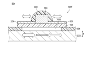
- Fig. 6A is a plan view showing a stretchable device according to a fifth embodiment of the present invention.
- Fig. 6B is a schematic cross-sectional view taken along line VIB-VIB in Fig. 6A.
- the fifth embodiment differs from the first embodiment in that the adhesive layer 60X has a discontinuous region 70X.
- the adhesive layer 60X has one main surface 61X attached to the stretchable substrate 10X and the other main surface 62X configured to be attached to a living body 200X (see Figures 6A and 6B).
- the discontinuous region 70X of the adhesive layer 60X is positioned in a portion that overlaps with the electronic component 50X when viewed from the thickness direction X of the stretchable substrate 10X.
- the electronic component 50X and the continuous region of the adhesive layer 60X do not overlap when viewed from the thickness direction X of the stretchable substrate 10X.
- the living body 200X and the stretchable substrate 10X may be in partial contact.
- Fig. 7A is a plan view showing a stretchable device according to a sixth embodiment of the present invention.
- Fig. 7B is a schematic cross-sectional view taken along line VIIB-VIIB in Fig. 7A.
- the sixth embodiment differs from the fifth embodiment in that it further includes a sealing resin 80X that covers the electronic component 50X.
- the inner edge 62X of the continuous region 64X of the adhesive layer 60X is located inside the outer edge 81X of the sealing resin 80X, stress is likely to concentrate at the interface between the stretchable and non-stretchable parts of the stretchable device 100E.
- the "inner side” here refers to the side where the shortest distance to the electronic component 50X is shorter, based on the position of the electronic component 50X. In other words, the side where the shortest distance to the electronic component 50X is longer may correspond to the outside.
- the inner edge 62X of the continuous region 64X of the adhesive layer 60X be positioned outside the outer edge 81X of the sealing resin 80X. This makes it possible to effectively prevent breakage of the components when the device 100E expands or contracts.
- the inner edge 62X of the continuous region 64X of the adhesive layer 60X and the outer edge 81X of the sealing resin 80X may be on a coaxial line.
- the living body 200X and the stretchable substrate 10X may be in partial contact.
- Fig. 8 is a schematic cross-sectional view showing a modification of Fig. 7B.
- the seventh embodiment differs from the sixth embodiment in that the width of the discontinuous region 70X1 of the adhesive layer 60X is larger.
- the width of the discontinuous region 70X1 of the adhesive layer 60X is large, as shown in FIG. 8, even if the elongation on the living body 200X side differs from one another in the region below the electronic component 50X, the action of the stretching force on the mounted non-stretchable electronic component 50X can be more suitably suppressed.
- the living body 200X and the stretchable substrate 10X do not come into contact even partially.
- the width of the discontinuous region 70X1 in cross-sectional view is preferably at least twice as wide as the electronic component 50X, and more preferably at least three times as wide. Furthermore, it is even more preferable that the width of each region that constitutes the discontinuous region 70X1 in the substrate thickness direction X and that is located on both sides of the electronic component 50 in cross-sectional view is at least the width of the electronic component 50X.
- the stretchable device may have the following features.
- the present invention comprises a stretchable substrate, a stretchable wiring provided on one main surface of the stretchable substrate, an electronic component provided so as to be electrically connectable to the stretchable wiring, and an adhesive layer provided on the other main surface of the stretchable substrate, A stretchable device, wherein at least one of the stretchable substrate and the adhesive layer has discontinuous regions.
- the elastic wiring includes a connection portion that can be electrically connected to the electronic component, When the stretchable substrate has the discontinuous region, the discontinuous region of the stretchable substrate is disposed around the connection portion when viewed in a thickness direction of the stretchable substrate.
- the stretchable wiring has the connection portion and an extension portion continuous with the connection portion, and a longitudinal portion of the discontinuous region extends at least along a direction parallel to the extension direction of the extension portion of the stretchable wiring.
- the electronic component has a main body portion and first and second electrode portions provided on the main body portion facing each other, and at least the main body portion is non-stretchable.
- ⁇ 5> The stretchable device according to any one of ⁇ 1> to ⁇ 4>, wherein the discontinuous region is a through hole.
- ⁇ 6> The stretchable device according to any one of ⁇ 1> to ⁇ 4>, wherein the discontinuous region has a groove shape.
- ⁇ 7> The stretchable device according to any one of ⁇ 1> to ⁇ 6>, wherein the ratio of depth to width of the discontinuous region is 1:2.
- ⁇ 8> The extension portion of the stretchable wiring extends in one direction, and the discontinuous region is arranged in a direction intersecting the extension direction of the extension portion.
- the extension portion of the elastic wiring has a first extension region continuous with the connection portion and a second extension region extending in a direction different from the first extension region,
- the electronic component has a main body and first and second electrode parts provided on the main body and facing each other, the first electrode part is electrically connected to the connection part of the first stretchable wiring, the second electrode part is electrically connected to the connection part of the second stretchable wiring, and the discontinuous region is continuous from the periphery of the connection part of the first stretchable wiring to the periphery of the connection part of the second stretchable wiring.
- the stretchable device according to any one of ⁇ 1> to ⁇ 10>.
- ⁇ 12> The stretchable device according to any one of ⁇ 1> to ⁇ 11>, wherein, in a planar view, the discontinuous region is arranged so as to entirely surround the outer edge of the connection portion of the stretchable wiring.
- the shortest distance between the discontinuous region and the connection portion of the stretchable wiring is 5% to 50% of the shortest distance between the outer edge of the stretchable substrate and the connection portion.
- ⁇ 14> In a cross-sectional view, the stretchable substrate and the electronic component are separated from each other, and a protective layer is provided between the stretchable substrate and the electronic component.
- ⁇ 15> The stretchable device according to any one of ⁇ 1> to ⁇ 14>, wherein a covering layer is provided to cover the stretchable substrate and the electronic component in a cross-sectional view.
- ⁇ 16> The stretchable device according to ⁇ 14> or ⁇ 15>, wherein the discontinuous region extends continuously from the stretchable substrate to the protective layer and/or the covering layer.
- ⁇ 17> The stretchable device according to any one of ⁇ 1> to ⁇ 16>, wherein the width of the discontinuous region is 100 ⁇ m or more.
- the adhesive layer is capable of being attached to a living body, The stretchable device according to ⁇ 1>, wherein when the adhesive layer has the discontinuous region, the discontinuous region of the adhesive layer is positioned in a portion overlapping the electronic component.
- ⁇ 19> Further comprising a sealing resin for covering the electronic components, The stretchable device according to ⁇ 18>, wherein an inner edge of the continuous region of the adhesive layer is located outside an outer edge of the sealing resin.
Landscapes
- Engineering & Computer Science (AREA)
- Microelectronics & Electronic Packaging (AREA)
- Laminated Bodies (AREA)
- Structure Of Printed Boards (AREA)
Priority Applications (1)
| Application Number | Priority Date | Filing Date | Title |
|---|---|---|---|
| JP2025516893A JP7794361B2 (ja) | 2023-04-26 | 2024-04-25 | 伸縮性デバイス |
Applications Claiming Priority (2)
| Application Number | Priority Date | Filing Date | Title |
|---|---|---|---|
| JP2023072342 | 2023-04-26 | ||
| JP2023-072342 | 2023-04-26 |
Publications (1)
| Publication Number | Publication Date |
|---|---|
| WO2024225388A1 true WO2024225388A1 (ja) | 2024-10-31 |
Family
ID=93256529
Family Applications (1)
| Application Number | Title | Priority Date | Filing Date |
|---|---|---|---|
| PCT/JP2024/016278 Ceased WO2024225388A1 (ja) | 2023-04-26 | 2024-04-25 | 伸縮性デバイス |
Country Status (2)
| Country | Link |
|---|---|
| JP (1) | JP7794361B2 (https=) |
| WO (1) | WO2024225388A1 (https=) |
Citations (4)
| Publication number | Priority date | Publication date | Assignee | Title |
|---|---|---|---|---|
| JP2019075500A (ja) * | 2017-10-18 | 2019-05-16 | 日本メクトロン株式会社 | 伸縮性配線基板、伸縮性配線基板の製造方法及び電子部品付伸縮性配線基板 |
| WO2019093144A1 (ja) * | 2017-11-10 | 2019-05-16 | 日東電工株式会社 | 貼付型生体センサ |
| JP2021034387A (ja) * | 2019-08-13 | 2021-03-01 | 日本メクトロン株式会社 | 伸縮性配線基板及び電気的筋肉刺激装置 |
| JP2021064681A (ja) * | 2019-10-11 | 2021-04-22 | 大日本印刷株式会社 | 配線基板及び配線基板の製造方法 |
-
2024
- 2024-04-25 JP JP2025516893A patent/JP7794361B2/ja active Active
- 2024-04-25 WO PCT/JP2024/016278 patent/WO2024225388A1/ja not_active Ceased
Patent Citations (4)
| Publication number | Priority date | Publication date | Assignee | Title |
|---|---|---|---|---|
| JP2019075500A (ja) * | 2017-10-18 | 2019-05-16 | 日本メクトロン株式会社 | 伸縮性配線基板、伸縮性配線基板の製造方法及び電子部品付伸縮性配線基板 |
| WO2019093144A1 (ja) * | 2017-11-10 | 2019-05-16 | 日東電工株式会社 | 貼付型生体センサ |
| JP2021034387A (ja) * | 2019-08-13 | 2021-03-01 | 日本メクトロン株式会社 | 伸縮性配線基板及び電気的筋肉刺激装置 |
| JP2021064681A (ja) * | 2019-10-11 | 2021-04-22 | 大日本印刷株式会社 | 配線基板及び配線基板の製造方法 |
Also Published As
| Publication number | Publication date |
|---|---|
| JPWO2024225388A1 (https=) | 2024-10-31 |
| JP7794361B2 (ja) | 2026-01-06 |
Similar Documents
| Publication | Publication Date | Title |
|---|---|---|
| US10096570B2 (en) | Manufacturing method for power semiconductor device, and power semiconductor device | |
| KR102213604B1 (ko) | 반도체 패키지 장치 | |
| KR101486137B1 (ko) | 방열 장치 및 그 제조 방법 | |
| US20100244234A1 (en) | Semiconductor device and method of manufacturing same | |
| JP2008226946A (ja) | 半導体装置およびその製造方法 | |
| US20100308457A1 (en) | Semiconductor apparatus and manufacturing method of the same | |
| CN103972277B (zh) | 半导体装置及其制造方法 | |
| JP2007329362A (ja) | パワーモジュール | |
| TWI699147B (zh) | 軟性電路板及包括其的電子裝置 | |
| CN102881804B (zh) | 基板结构、半导体装置阵列及其半导体装置 | |
| US9484294B2 (en) | Semiconductor device and method of manufacturing the same | |
| TWI693866B (zh) | 軟性電路板及其製造方法 | |
| WO2024225388A1 (ja) | 伸縮性デバイス | |
| JP6422736B2 (ja) | パワーモジュール | |
| US20110068462A1 (en) | Semiconductor chip packages having reduced stress | |
| JP4904623B2 (ja) | 光半導体素子 | |
| US9196602B2 (en) | High power dielectric carrier with accurate die attach layer | |
| JP2011077164A (ja) | 半導体発光装置 | |
| US12519047B2 (en) | Semiconductor device | |
| CN103280438B (zh) | 具有准确芯片附着层的大功率介电载体 | |
| JP6603098B2 (ja) | 回路基板および電子装置 | |
| JP2007266150A (ja) | 熱伝導性接合材、半導体パッケージ、ヒートスプレッダ、半導体チップ、及び半導体チップとヒートスプレッダとを接合する接合方法 | |
| JPH0342860A (ja) | フレキシブルプリント配線板 | |
| KR101716882B1 (ko) | 접속 영역의 스트레스가 분산되는 연성 패키지, 및 그 제조 방법 | |
| US8101462B2 (en) | Method for manufacturing semiconductor device, and semiconductor device |
Legal Events
| Date | Code | Title | Description |
|---|---|---|---|
| 121 | Ep: the epo has been informed by wipo that ep was designated in this application |
Ref document number: 24797133 Country of ref document: EP Kind code of ref document: A1 |
|
| ENP | Entry into the national phase |
Ref document number: 2025516893 Country of ref document: JP Kind code of ref document: A |
|
| WWE | Wipo information: entry into national phase |
Ref document number: 2025516893 Country of ref document: JP |
|
| NENP | Non-entry into the national phase |
Ref country code: DE |
|
| 122 | Ep: pct application non-entry in european phase |
Ref document number: 24797133 Country of ref document: EP Kind code of ref document: A1 |