WO2024214783A1 - 印刷版及びその製造方法 - Google Patents
印刷版及びその製造方法 Download PDFInfo
- Publication number
- WO2024214783A1 WO2024214783A1 PCT/JP2024/014686 JP2024014686W WO2024214783A1 WO 2024214783 A1 WO2024214783 A1 WO 2024214783A1 JP 2024014686 W JP2024014686 W JP 2024014686W WO 2024214783 A1 WO2024214783 A1 WO 2024214783A1
- Authority
- WO
- WIPO (PCT)
- Prior art keywords
- halftone dot
- printing plate
- dot pattern
- negative film
- dots
- Prior art date
- Legal status (The legal status is an assumption and is not a legal conclusion. Google has not performed a legal analysis and makes no representation as to the accuracy of the status listed.)
- Ceased
Links
Images





Classifications
-
- B—PERFORMING OPERATIONS; TRANSPORTING
- B41—PRINTING; LINING MACHINES; TYPEWRITERS; STAMPS
- B41N—PRINTING PLATES OR FOILS; MATERIALS FOR SURFACES USED IN PRINTING MACHINES FOR PRINTING, INKING, DAMPING, OR THE LIKE; PREPARING SUCH SURFACES FOR USE AND CONSERVING THEM
- B41N1/00—Printing plates or foils; Materials therefor
-
- B—PERFORMING OPERATIONS; TRANSPORTING
- B41—PRINTING; LINING MACHINES; TYPEWRITERS; STAMPS
- B41C—PROCESSES FOR THE MANUFACTURE OR REPRODUCTION OF PRINTING SURFACES
- B41C1/00—Forme preparation
-
- G—PHYSICS
- G02—OPTICS
- G02F—OPTICAL DEVICES OR ARRANGEMENTS FOR THE CONTROL OF LIGHT BY MODIFICATION OF THE OPTICAL PROPERTIES OF THE MEDIA OF THE ELEMENTS INVOLVED THEREIN; NON-LINEAR OPTICS; FREQUENCY-CHANGING OF LIGHT; OPTICAL LOGIC ELEMENTS; OPTICAL ANALOGUE/DIGITAL CONVERTERS
- G02F1/00—Devices or arrangements for the control of the intensity, colour, phase, polarisation or direction of light arriving from an independent light source, e.g. switching, gating or modulating; Non-linear optics
- G02F1/01—Devices or arrangements for the control of the intensity, colour, phase, polarisation or direction of light arriving from an independent light source, e.g. switching, gating or modulating; Non-linear optics for the control of the intensity, phase, polarisation or colour
- G02F1/13—Devices or arrangements for the control of the intensity, colour, phase, polarisation or direction of light arriving from an independent light source, e.g. switching, gating or modulating; Non-linear optics for the control of the intensity, phase, polarisation or colour based on liquid crystals, e.g. single liquid crystal display cells
-
- G—PHYSICS
- G02—OPTICS
- G02F—OPTICAL DEVICES OR ARRANGEMENTS FOR THE CONTROL OF LIGHT BY MODIFICATION OF THE OPTICAL PROPERTIES OF THE MEDIA OF THE ELEMENTS INVOLVED THEREIN; NON-LINEAR OPTICS; FREQUENCY-CHANGING OF LIGHT; OPTICAL LOGIC ELEMENTS; OPTICAL ANALOGUE/DIGITAL CONVERTERS
- G02F1/00—Devices or arrangements for the control of the intensity, colour, phase, polarisation or direction of light arriving from an independent light source, e.g. switching, gating or modulating; Non-linear optics
- G02F1/01—Devices or arrangements for the control of the intensity, colour, phase, polarisation or direction of light arriving from an independent light source, e.g. switching, gating or modulating; Non-linear optics for the control of the intensity, phase, polarisation or colour
- G02F1/13—Devices or arrangements for the control of the intensity, colour, phase, polarisation or direction of light arriving from an independent light source, e.g. switching, gating or modulating; Non-linear optics for the control of the intensity, phase, polarisation or colour based on liquid crystals, e.g. single liquid crystal display cells
- G02F1/133—Constructional arrangements; Operation of liquid crystal cells; Circuit arrangements
- G02F1/1333—Constructional arrangements; Manufacturing methods
- G02F1/1337—Surface-induced orientation of the liquid crystal molecules, e.g. by alignment layers
-
- B—PERFORMING OPERATIONS; TRANSPORTING
- B41—PRINTING; LINING MACHINES; TYPEWRITERS; STAMPS
- B41P—INDEXING SCHEME RELATING TO PRINTING, LINING MACHINES, TYPEWRITERS, AND TO STAMPS
- B41P2200/00—Printing processes
- B41P2200/10—Relief printing
- B41P2200/12—Flexographic printing
Definitions
- the present invention relates to a printing plate used in printing such as flexographic printing and a method for manufacturing the same.
- the liquid crystal panel includes an array substrate, a color filter substrate disposed opposite the array substrate, and a liquid crystal layer sandwiched therebetween.
- the array substrate includes, for example, a transparent substrate, a gate electrode, a gate insulating film, a semiconductor layer, a first protective film, a source electrode, a drain electrode, a second protective film, and a resin film.
- a contact hole is formed in such an array substrate, and the transparent electrode is electrically connected to the drain electrode at the bottom of the contact hole.
- an alignment film made of polyimide or the like is formed on the entire surface of the transparent electrodes of the array substrate so as to fill the contact holes.
- Methods for forming an alignment film by applying an alignment film material such as polyimide onto the transparent electrodes of the array substrate include printing methods such as flexography and inkjet methods.
- a printing plate P1 used in flexographic printing typically comprises a flat base 11 and a printing convex portion 12 formed in the center of the surface of the base 11.
- the printing convex portion 12 is the printing area, and the portion of the base 11 around the printing convex portion 12 does not participate in printing.
- 8(c) which is an enlarged cross-sectional view of a main portion of Fig. 8(b)
- gaps 14 are distributed between a plurality of protrusions 13 on the top surface of the printing convex portion 12, and ink is retained in the gaps 14.
- the printing plate P1 has flexibility so that it can be mounted along the peripheral side surface of the plate cylinder 51 (see Fig. 7).
- Fig. 9(a) is a perspective view showing a part of the protrusions 13 formed in the printing convex portion 12 of the general printing plate P1.
- Fig. 9(b) is a graph showing the height difference formed in the printing convex portion 12 by the protrusions 13 and the gaps 14 when the printing convex portion 12 is viewed in a side cross-sectional view. As shown in these figures, the multiple protrusions 13 are arranged orthogonally in the printing convex portion 12. Moreover, the protrusions 13 shown in Fig.
- ink alignment film material
- the ink is retained in the gaps 14 formed between the multiple protrusions 13 arranged orthogonally, and the retained ink is transferred from the printing plate P1 in this state to the printing substrate Q (such as the array substrate) (see Figure 7).
- the ink When ink is transferred to the print medium Q in this manner, localized unevenness in thickness may occur in the alignment film.
- the ink may be repelled by surface tension or by fine debris (residue) created when the contact holes were formed, preventing the ink from fully penetrating the contact holes, resulting in uneven thickness of the alignment film around the contact holes and uneven thickness.
- the liquid crystal panel is turned on (especially in mid-tones), the uneven thickness areas appear as uneven brightness and are easily visible.
- the contact holes CH formed in the array substrate 20 are usually arranged regularly.
- the printing plate P1 also has a plurality of protrusions 13 arranged regularly, and therefore the gaps 14 for holding ink are also arranged regularly. Therefore, the gaps 14 for holding ink abut against the contact holes CH and the gaps 14 for holding ink abut against the areas around the contact holes CH where ink repellency occurs are both regularly generated, resulting in regular unevenness in the thickness of the transferred ink, and therefore regular unevenness in the thickness of the alignment film. If there is regularity in the positions where the thickness unevenness occurs, the thickness unevenness becomes easily noticeable, which tends to cause a deterioration in the display quality of a liquid crystal panel manufactured using such an array substrate.
- the present invention has been developed in consideration of these circumstances, and provides a printing plate and a method for manufacturing the same that make uneven film thickness on the printing medium Q less noticeable.
- the printing plate of the present invention is a printing plate having a printing convex portion on a top surface of which a plurality of protrusions are formed, the protrusions are formed by placing a negative film having a predetermined shape on a photosensitive resin that will become a printing plate, and allowing light to pass through the predetermined shaped portion of the negative film and harden the photosensitive resin in the portion that is hit by the light;
- the predetermined shape formed on the negative film is a shape (E) in which two or more halftone dot patterns are superimposed on the same plane such that at least one of the dots in one halftone dot pattern overlaps with at least one of the dots in a different halftone dot pattern.
- the present invention also provides a method for producing a printing plate, the method comprising the steps of: preparing a negative film having a predetermined shape; placing the negative film on a photosensitive resin that will become a printing plate; and irradiating the photosensitive resin on which the negative film is placed with light through the negative film, thereby curing the photosensitive resin at a position where the light passes through the negative film,
- the printing plate has a printing convex portion having a plurality of protrusions formed on a top surface thereof
- the negative film preparation step forms a shape (E) on the negative film in which two or more halftone dot patterns are superimposed on the same plane such that at least one of the dots of one halftone dot pattern overlaps with at least one of the dots of a different halftone dot pattern
- the photosensitive resin hardening step light passes through the shape (E) portion formed on the negative film to harden the photosensitive resin on which the light strikes, and the protrusions are formed by the hardened portions.
- the thickness unevenness is easily noticeable. In other words, if the regularity is lost, the thickness unevenness becomes less noticeable.
- the present inventors have focused on this point and discovered that by suppressing the regular occurrence of the above-mentioned thickness unevenness, the thickness unevenness can be made less noticeable.
- the printing plate is characterized in that the predetermined shape formed on the negative film is a shape (E) in which two or more halftone dot patterns are superimposed on the same plane such that at least one of the dots of one halftone dot pattern overlaps with at least one of the dots of a different halftone dot pattern.
- ⁇ 1 is the angle between an imaginary line M' connecting the centers of adjacent dots in the row direction in dot pattern M and an imaginary line M1' connecting the centers of adjacent dots in the row direction in dot pattern M1.
- the printing plate according to [4] has a plurality of halftone dot patterns to be superimposed on the base, and when the intersection point RP is an intersection point of imaginary lines connecting the centers of adjacent halftone dots in the row direction in each halftone dot pattern, the imaginary line M' of the base halftone dot pattern passes through the intersection point RP, and the multiple imaginary lines of the halftone dot patterns to be superimposed on the base are angled differently from each other with respect to the imaginary line M' of the base halftone dot pattern.
- a method for producing a printing plate comprising the steps of: preparing a negative film having a predetermined shape; placing the negative film on a photosensitive resin that will become a printing plate; and irradiating the photosensitive resin on which the negative film is placed with light through the negative film, thereby curing the photosensitive resin at a position where the light passes through the negative film,
- the printing plate has a printing convex portion having a plurality of protrusions formed on a top surface thereof
- the negative film preparation step forms a shape (E) on the negative film in which two or more halftone dot patterns are superimposed on the same plane such that at least one of the dots of one halftone dot pattern overlaps with at least one of the dots of a different halftone dot pattern
- a method for producing a printing plate characterized in that in the photosensitive resin hardening step, light passes through the shape (E) portion formed on the negative film to harden the photosensitive resin exposed to the light, and the protrusions are formed by the hardened portions.
- the printing plate of the present invention has a top surface shape of the protrusions that is formed to be the same as the shape (E-shape) of two or more halftone dot patterns superimposed on the same plane such that at least one of the points of one halftone dot pattern overlaps with at least one of the points of a different halftone dot pattern.
- This breaks down the regularity of the protrusions and gaps, making it possible to suppress the occurrence of regular unevenness in the film thickness of the alignment film provided on the array substrate. As a result, the unevenness in the film thickness can be made less noticeable.
- the halftone dot pattern has halftone dots arranged at equal intervals in the row and column directions, the halftone dot pattern itself is easy to create, and the regularity of the protrusions and gaps can be more easily disrupted.
- the method for manufacturing a printing plate of the present invention includes the steps of placing a negative film having the shape (E) below formed thereon on a photosensitive resin that will become the printing plate, and irradiating light onto the photosensitive resin on which the negative film is placed, and curing the photosensitive resin at the position where the light passes through the negative film.
- This makes it possible to make the top shape of the protrusions correspond to the shape (E) below, and to form a printing plate that is free of regularity in the protrusions and gaps.
- (E) A shape in which two or more halftone dot patterns are superimposed on the same plane with their positions shifted from each other.
- the halftone dot pattern has halftone dots arranged at equal intervals in the row and column directions, the regularity of the protrusions and gaps can be broken down even more effectively.
- FIG. 10E is a diagram for explaining an example of a procedure for creating a shape.
- FIG. 2 is an explanatory diagram showing an arrangement of contact holes formed in an array substrate.
- FIG. 1 is an explanatory diagram illustrating a printing press that uses printing plates. 1A is a plan view of a conventional printing plate, FIG. 1B is a cross-sectional view taken along line T-T of FIG. 1A, and FIG.
- FIG. 1C is an enlarged cross-sectional view of a main part of FIG. 1A is an oblique view showing a portion of a protrusion formed on a printing convex portion
- FIG. 1B is a graph showing the height difference formed on the printing convex portion by the protrusion and the gap when the printing convex portion is viewed in side cross-section.
- FIG. 1A is a diagram illustrating a negative film used in the manufacture of a printing plate of the present invention
- FIG. 1B is a diagram illustrating a method of manufacturing a printing plate using the negative film.
- FIG. 1(a) is a plan view showing one embodiment of a printing plate of the present invention
- (b) is an enlarged view of the essential parts of the R-R cross section of (a)
- (c) is an enlarged view of the essential parts of the cross section of (b).
- the printing plate P according to one embodiment of the present invention comprises a flat base 1 that is rectangular in plan view, and a printing protrusion 2 that is rectangular in plan view formed in the center of the surface of the base 1, with a plurality of protrusions 3 and gaps 4 (see FIG. 2(a)) distributed on the top surface of the printing protrusion 2.
- the printing plate P is used for flexographic printing.
- the printing plate P is flexible so that it can be attached to the peripheral surface of the plate cylinder 51 of a printing press (see FIG. 7).
- the printing plate P is formed from a material such as photosensitive resin, rubber, etc.
- the base 1, printing convex portion 2, and protrusions 3 are integrally formed.
- the direction of the arrow along the long side of the printing convex portion 2, which is rectangular in plan view, is set as the printing direction.
- gaps 4 are distributed among the multiple protrusions 3, as shown below, and ink is held in the gaps 4.
- Figure 2(a) is an oblique view showing a part of a protrusion 3 formed on the printing convex portion 2
- Figure 2(b) is a graph showing the height difference formed in the printing convex portion 2 by the above-mentioned protrusion 3 and gap portion 4 when the printing convex portion 2 is viewed in side cross-section.
- the protrusions 3 and the gaps 4 are formed in the printing convex portion 2 in a non-regular manner.
- 2(a) have, for example, a maximum depth of 15.7 ⁇ m and a cell volume of 3.69 cm3 / cm2 , which is approximately the same as that of a conventional printing plate in which multiple protrusions are regularly arranged. It should be noted that the shapes of the printing convex portions 2 shown in Figs. 1(c), 2(a) and 2(b) are merely examples, and the shapes do not coincide with each other.
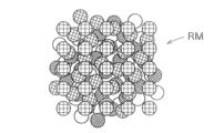
- FIG. 3 is a diagram showing an example of the (E) shape in the present invention.
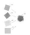
- the pattern RM shown in FIG. 3 is formed by using any number of halftone dot patterns, two or more (four in this example, see FIG. 5), and overlapping them on the same plane so that at least one of the dots in one halftone dot pattern overlaps with at least one of the dots in a different halftone dot pattern.
- the halftone dot patterns may be the same as each other, or may have different line numbers, etc. However, it is preferable to use patterns with different line numbers, etc., in order to further suppress the occurrence of moire.
- the halftone dot pattern in the present invention may be any pattern in which the halftone dots are arranged with regularity, and the regularity may differ between the row and column directions. However, if the halftone dots are arranged at equal intervals in the row and column directions, the shape (E) with the regularity disrupted can be created more reliably by calculation.
- the term "halftone dots" refers to dots arranged in a mesh pattern to express the shades of a printed matter, but in the present invention, the term is not limited to dots that express the shades of a printed matter, but refers to dots in general that are arranged in a mesh pattern with a predetermined regularity.
- FIG. 4(a) shows a halftone dot pattern M showing an arrangement of halftone dots
- FIG. 4(b) shows the base halftone dot pattern M and halftone dot patterns M1 to M3 to be superimposed on the base.
- the angle ⁇ 1 between a virtual line M' connecting the centers (Mc) of adjacent dots in the row direction in the base dot pattern M and a virtual line M1' connecting the centers (M1c) of adjacent dots in the row direction in the dot pattern M1 to be superimposed on the base satisfy the following formula (1), in order to further disrupt the regularity.
- the angle between each virtual line and the virtual line M' satisfy the following formula (1). 0° ⁇ 1 ⁇ 90°...(1)
- the intersection point RP is the imaginary line connecting the centers of adjacent halftone dots in the row direction (M1c, M2c, M3c, ...) in these halftone dot patterns
- the imaginary line M' of the base halftone dot pattern passes through the intersection point RP and the multiple imaginary lines of the halftone dot patterns to be superimposed on the base are angled differently relative to the imaginary line M' of the base halftone dot pattern, as this can more reliably disrupt the regularity.
- the angles ⁇ 1 , ⁇ 2 , ⁇ 3 formed by these imaginary lines satisfy the relationship 0° ⁇ ⁇ 1 ⁇ ⁇ 2 ⁇ ⁇ 3 ⁇ 90°, and it is even more preferable that the angles are separated by 10° or more.
- the pattern RM shown in Figure 3 is a superposition of the halftone dot patterns M, M1 to M3, which have different specifications, as shown in Figure 5.
- Pattern RM is drawn and made into a negative, and a negative film (mask) for forming a printing plate is created using the negative-positive principle.
- a pattern RM with disrupted regularity is formed.
- the pattern RM is formed using four halftone dot patterns M, M1 to M3, but the pattern RM can be formed using two or more halftone dot patterns and is not limited to four halftone dot patterns.
- the shape of the pattern RM formed by overlapping multiple halftone dot patterns can be made infinite, but it is preferable to select a combination that generates as little unusual unevenness as possible.
- a pattern RM in which four or more halftone dot patterns are superimposed.
- the negative film preparation step involves forming a shape (E) on the negative film by overlapping two or more halftone dot patterns on the same plane such that at least one of the dots of one halftone dot pattern overlaps at least one of the dots of a different halftone dot pattern
- the portions of the photosensitive resin that are hit by light passing through the portions of shape (E) formed on the negative film become the protrusions 3.
- the portions of the photosensitive resin that are not hit by light because light does not pass through the negative film become the gaps 4.
- FIGS. 10(a) and (b) are diagrams for explaining a method for producing the printing plate P by photolithography.
- a negative film is prepared in which two or more halftone dot patterns are superimposed on the same plane such that at least one of the dots of one halftone dot pattern overlaps at least one of the dots of a different halftone dot pattern, forming a shape (E) as a light transmitting portion.
- the light transmitting portions of the negative film are shown as white.
- the photosensitive resin 6 on which the negative film 5 is placed is placed between the workpiece stage glass 8 and the workpiece glass cover 7, and light is irradiated in the direction indicated by the arrow.
- the obtained printing plate P is suitable for use as a printing plate for flexographic printing.
- Figure 7 shows an example of a flexographic printing press. This press is equipped with a cylindrical plate cylinder 51 on which the printing plate P is mounted, an anilox roll 52 that applies ink to the printing plate P, an ink supply device 53 that supplies ink to the surface of the anilox roll 52, a doctor blade 54 that scrapes off excess ink from the surface of the anilox roll 52, and a printing stage 55 on which the printing medium Q to be printed is placed.
- Flexographic printing with the above printing press is performed as follows. That is, printing plate P is attached to the peripheral surface of plate cylinder 51, and while the plate cylinder 51 is rotating, ink supplied from ink supply device 53 is applied to the printing area of printing plate P via anilox roll 52, and the applied ink is transferred to a printing material Q such as a glass substrate placed on printing stage 55, thereby printing. At this time, printing stage 55 is slid in the direction of the arrow in synchronization with the rotation of plate cylinder 51.
- ink When ink is transferred to the substrate Q in this manner, typically when the substrate Q is an array substrate 20, the ink is repelled around the contact holes CH due to surface tension and fine debris (residue) generated during the formation of the contact holes, and the ink does not fully penetrate into the contact holes CH, resulting in an uneven ink film thickness around the contact holes CH and an uneven film thickness in the resulting alignment film.
- the protrusions 3 and gaps 4 are formed in a disordered manner on the printing convex portion 2 of the printing plate P of the present invention, even if the contact holes CH are formed in a regular arrangement on the array substrate 20, unevenness in the thickness of the alignment film will not occur regularly, and even if unevenness in the thickness does occur, it will be difficult to notice.
- the printing plate of the present invention can be useful as a printing plate in which unevenness in film thickness is less noticeable.
Landscapes
- Physics & Mathematics (AREA)
- Nonlinear Science (AREA)
- General Physics & Mathematics (AREA)
- Chemical & Material Sciences (AREA)
- Crystallography & Structural Chemistry (AREA)
- Optics & Photonics (AREA)
- Mathematical Physics (AREA)
- Spectroscopy & Molecular Physics (AREA)
- Engineering & Computer Science (AREA)
- Manufacturing & Machinery (AREA)
- Manufacture Or Reproduction Of Printing Formes (AREA)
- Printing Plates And Materials Therefor (AREA)
- Photosensitive Polymer And Photoresist Processing (AREA)
Priority Applications (3)
| Application Number | Priority Date | Filing Date | Title |
|---|---|---|---|
| JP2025514011A JPWO2024214783A1 (https=) | 2023-04-14 | 2024-04-11 | |
| CN202480005749.7A CN120390694B (zh) | 2023-04-14 | 2024-04-11 | 印刷版及其制造方法 |
| KR1020257020392A KR102894165B1 (ko) | 2023-04-14 | 2024-04-11 | 인쇄판 및 그 제조 방법 |
Applications Claiming Priority (2)
| Application Number | Priority Date | Filing Date | Title |
|---|---|---|---|
| JP2023066518 | 2023-04-14 | ||
| JP2023-066518 | 2023-04-14 |
Publications (1)
| Publication Number | Publication Date |
|---|---|
| WO2024214783A1 true WO2024214783A1 (ja) | 2024-10-17 |
Family
ID=93059379
Family Applications (1)
| Application Number | Title | Priority Date | Filing Date |
|---|---|---|---|
| PCT/JP2024/014686 Ceased WO2024214783A1 (ja) | 2023-04-14 | 2024-04-11 | 印刷版及びその製造方法 |
Country Status (5)
| Country | Link |
|---|---|
| JP (1) | JPWO2024214783A1 (https=) |
| KR (1) | KR102894165B1 (https=) |
| CN (1) | CN120390694B (https=) |
| TW (1) | TW202446179A (https=) |
| WO (1) | WO2024214783A1 (https=) |
Citations (8)
| Publication number | Priority date | Publication date | Assignee | Title |
|---|---|---|---|---|
| JPH08286191A (ja) * | 1995-04-18 | 1996-11-01 | Citizen Watch Co Ltd | 液晶表示パネルおよびその製造方法 |
| US20010029859A1 (en) * | 1999-05-14 | 2001-10-18 | Mark Samworth | Screened film intermediate for use with flexographic printing plate having improved solids rendition |
| JP2014133335A (ja) * | 2013-01-09 | 2014-07-24 | Sumitomo Rubber Ind Ltd | フレキソ印刷版とその製造方法、ならびに液晶パネル用基板の製造方法 |
| WO2015056703A1 (ja) * | 2013-10-17 | 2015-04-23 | 富士フイルム株式会社 | フレキソ印刷版 |
| WO2017119236A1 (ja) * | 2016-01-04 | 2017-07-13 | 富士フイルム株式会社 | フレキソ印刷版、フレキソ印刷版原版、および、これらの製造方法 |
| JP2017164979A (ja) * | 2016-03-16 | 2017-09-21 | 株式会社コムラテック | 印刷版 |
| JP2018517939A (ja) * | 2015-06-02 | 2018-07-05 | イー・アイ・デュポン・ドウ・ヌムール・アンド・カンパニーE.I.Du Pont De Nemours And Company | 印刷版原版、原版の製造方法、及び原版からの印刷版の作製方法 |
| JP2019014133A (ja) * | 2017-07-06 | 2019-01-31 | 住友ゴム工業株式会社 | フレキソ印刷版の製造方法、および液晶表示素子の製造方法 |
Family Cites Families (7)
| Publication number | Priority date | Publication date | Assignee | Title |
|---|---|---|---|---|
| JP3103687B2 (ja) * | 1992-10-02 | 2000-10-30 | 京セラ株式会社 | 液晶セル用配向膜の形成法 |
| JP4080839B2 (ja) * | 2002-10-21 | 2008-04-23 | シャープ株式会社 | フレキソ印刷版の製造方法および印刷物の製造方法 |
| JP2007171546A (ja) * | 2005-12-22 | 2007-07-05 | Sharp Corp | 配向膜溶液印刷用版の修正方法 |
| JP5671784B2 (ja) * | 2009-04-02 | 2015-02-18 | 凸版印刷株式会社 | 印刷用凸版及びその印刷用凸版を用いた電子デバイスの製造方法並びに有機エレクトロルミネッセンス素子 |
| JP2012011666A (ja) * | 2010-06-30 | 2012-01-19 | Sharp Corp | フレキソ印刷装置、および該フレキソ印刷装置に備えるフレキソ印刷版、ならびに該フレキソ印刷版の製造方法 |
| JP2012078445A (ja) * | 2010-09-30 | 2012-04-19 | Asahi Kasei E-Materials Corp | マスクフィルム、感光性樹脂印刷版の製造方法、感光性樹脂印刷版 |
| JP6278942B2 (ja) * | 2015-10-21 | 2018-02-14 | 日本航空電子工業株式会社 | フレキソ印刷による絶縁膜の形成方法 |
-
2024
- 2024-04-11 TW TW113113467A patent/TW202446179A/zh unknown
- 2024-04-11 CN CN202480005749.7A patent/CN120390694B/zh active Active
- 2024-04-11 KR KR1020257020392A patent/KR102894165B1/ko active Active
- 2024-04-11 WO PCT/JP2024/014686 patent/WO2024214783A1/ja not_active Ceased
- 2024-04-11 JP JP2025514011A patent/JPWO2024214783A1/ja active Pending
Patent Citations (8)
| Publication number | Priority date | Publication date | Assignee | Title |
|---|---|---|---|---|
| JPH08286191A (ja) * | 1995-04-18 | 1996-11-01 | Citizen Watch Co Ltd | 液晶表示パネルおよびその製造方法 |
| US20010029859A1 (en) * | 1999-05-14 | 2001-10-18 | Mark Samworth | Screened film intermediate for use with flexographic printing plate having improved solids rendition |
| JP2014133335A (ja) * | 2013-01-09 | 2014-07-24 | Sumitomo Rubber Ind Ltd | フレキソ印刷版とその製造方法、ならびに液晶パネル用基板の製造方法 |
| WO2015056703A1 (ja) * | 2013-10-17 | 2015-04-23 | 富士フイルム株式会社 | フレキソ印刷版 |
| JP2018517939A (ja) * | 2015-06-02 | 2018-07-05 | イー・アイ・デュポン・ドウ・ヌムール・アンド・カンパニーE.I.Du Pont De Nemours And Company | 印刷版原版、原版の製造方法、及び原版からの印刷版の作製方法 |
| WO2017119236A1 (ja) * | 2016-01-04 | 2017-07-13 | 富士フイルム株式会社 | フレキソ印刷版、フレキソ印刷版原版、および、これらの製造方法 |
| JP2017164979A (ja) * | 2016-03-16 | 2017-09-21 | 株式会社コムラテック | 印刷版 |
| JP2019014133A (ja) * | 2017-07-06 | 2019-01-31 | 住友ゴム工業株式会社 | フレキソ印刷版の製造方法、および液晶表示素子の製造方法 |
Also Published As
| Publication number | Publication date |
|---|---|
| JPWO2024214783A1 (https=) | 2024-10-17 |
| CN120390694A (zh) | 2025-07-29 |
| CN120390694B (zh) | 2025-12-05 |
| KR20250099266A (ko) | 2025-07-01 |
| KR102894165B1 (ko) | 2025-12-01 |
| TW202446179A (zh) | 2024-11-16 |
Similar Documents
| Publication | Publication Date | Title |
|---|---|---|
| TWI249063B (en) | Display device and manufacturing method thereof | |
| JP2004212978A (ja) | 配向膜形成方法 | |
| JP4084290B2 (ja) | 液晶表示素子の製造方法 | |
| JP2002293049A (ja) | 薄膜形成用樹脂凸版 | |
| CN101301827A (zh) | 凹版凸胶印的印刷版及其制造方法,制造基板和显示器装置的方法 | |
| JP2005141235A (ja) | 配向膜形成装置及びその形成方法 | |
| WO2004007209A1 (ja) | 印刷版、印刷機および印刷方法ならびに液晶機器の製造装置および製造方法 | |
| JP5147201B2 (ja) | パターン形成方法及びこれを用いた液晶表示素子の製造方法 | |
| CN120390693B (zh) | 印刷版 | |
| WO2017159415A1 (ja) | 印刷版 | |
| WO2024214783A1 (ja) | 印刷版及びその製造方法 | |
| KR19980032956A (ko) | 로타리 릴리프 인쇄방법용 프린트 폼 | |
| KR101394571B1 (ko) | 배향막 형성용 전사판 | |
| WO2021166114A1 (ja) | 印刷装置、及び印刷物の製造方法 | |
| JP2012011666A (ja) | フレキソ印刷装置、および該フレキソ印刷装置に備えるフレキソ印刷版、ならびに該フレキソ印刷版の製造方法 | |
| JP2006240283A (ja) | 弾性樹脂版 | |
| JP2010091670A (ja) | カラーフィルタの製造方法 | |
| JP7846065B2 (ja) | フレキソ印刷版 | |
| KR101023724B1 (ko) | 액정표시장치용 배향막 인쇄장치의 수지 플레이트 및 이의제조방법 | |
| JP2008287902A (ja) | 有機elディスプレイの製造方法及び有機elディスプレイ | |
| JP2002122723A (ja) | カラーフィルタ及びその製造方法並びにそれを用いた液晶表示装置及びその製造方法 | |
| JP2009148901A (ja) | 高精度凸版 | |
| JP2010122298A (ja) | カラーフィルタの製造方法 | |
| JPH0756161A (ja) | 液晶表示素子 | |
| JP2007102231A (ja) | 表示板及びその製造方法 |
Legal Events
| Date | Code | Title | Description |
|---|---|---|---|
| 121 | Ep: the epo has been informed by wipo that ep was designated in this application |
Ref document number: 24788805 Country of ref document: EP Kind code of ref document: A1 |
|
| WWE | Wipo information: entry into national phase |
Ref document number: 2025514011 Country of ref document: JP |
|
| ENP | Entry into the national phase |
Ref document number: 20257020392 Country of ref document: KR Kind code of ref document: A |
|
| WWE | Wipo information: entry into national phase |
Ref document number: 1020257020392 Country of ref document: KR Ref document number: 202480005749.7 Country of ref document: CN |
|
| WWP | Wipo information: published in national office |
Ref document number: 1020257020392 Country of ref document: KR |
|
| WWP | Wipo information: published in national office |
Ref document number: 202480005749.7 Country of ref document: CN |
|
| NENP | Non-entry into the national phase |
Ref country code: DE |
|
| 122 | Ep: pct application non-entry in european phase |
Ref document number: 24788805 Country of ref document: EP Kind code of ref document: A1 |