WO2024203720A1 - 配線基板 - Google Patents
配線基板 Download PDFInfo
- Publication number
- WO2024203720A1 WO2024203720A1 PCT/JP2024/011014 JP2024011014W WO2024203720A1 WO 2024203720 A1 WO2024203720 A1 WO 2024203720A1 JP 2024011014 W JP2024011014 W JP 2024011014W WO 2024203720 A1 WO2024203720 A1 WO 2024203720A1
- Authority
- WO
- WIPO (PCT)
- Prior art keywords
- conductor
- metal body
- wiring
- base
- wiring board
- Prior art date
- Legal status (The legal status is an assumption and is not a legal conclusion. Google has not performed a legal analysis and makes no representation as to the accuracy of the status listed.)
- Ceased
Links
Images





Classifications
-
- H—ELECTRICITY
- H05—ELECTRIC TECHNIQUES NOT OTHERWISE PROVIDED FOR
- H05K—PRINTED CIRCUITS; CASINGS OR CONSTRUCTIONAL DETAILS OF ELECTRIC APPARATUS; MANUFACTURE OF ASSEMBLAGES OF ELECTRICAL COMPONENTS
- H05K1/00—Printed circuits
- H05K1/02—Details
-
- H—ELECTRICITY
- H05—ELECTRIC TECHNIQUES NOT OTHERWISE PROVIDED FOR
- H05K—PRINTED CIRCUITS; CASINGS OR CONSTRUCTIONAL DETAILS OF ELECTRIC APPARATUS; MANUFACTURE OF ASSEMBLAGES OF ELECTRICAL COMPONENTS
- H05K1/00—Printed circuits
- H05K1/02—Details
- H05K1/11—Printed elements for providing electric connections to or between printed circuits
-
- H—ELECTRICITY
- H05—ELECTRIC TECHNIQUES NOT OTHERWISE PROVIDED FOR
- H05K—PRINTED CIRCUITS; CASINGS OR CONSTRUCTIONAL DETAILS OF ELECTRIC APPARATUS; MANUFACTURE OF ASSEMBLAGES OF ELECTRICAL COMPONENTS
- H05K3/00—Apparatus or processes for manufacturing printed circuits
-
- H—ELECTRICITY
- H05—ELECTRIC TECHNIQUES NOT OTHERWISE PROVIDED FOR
- H05K—PRINTED CIRCUITS; CASINGS OR CONSTRUCTIONAL DETAILS OF ELECTRIC APPARATUS; MANUFACTURE OF ASSEMBLAGES OF ELECTRICAL COMPONENTS
- H05K3/00—Apparatus or processes for manufacturing printed circuits
- H05K3/10—Apparatus or processes for manufacturing printed circuits in which conductive material is applied to the insulating support in such a manner as to form the desired conductive pattern
- H05K3/18—Apparatus or processes for manufacturing printed circuits in which conductive material is applied to the insulating support in such a manner as to form the desired conductive pattern using precipitation techniques to apply the conductive material
-
- H—ELECTRICITY
- H05—ELECTRIC TECHNIQUES NOT OTHERWISE PROVIDED FOR
- H05K—PRINTED CIRCUITS; CASINGS OR CONSTRUCTIONAL DETAILS OF ELECTRIC APPARATUS; MANUFACTURE OF ASSEMBLAGES OF ELECTRICAL COMPONENTS
- H05K3/00—Apparatus or processes for manufacturing printed circuits
- H05K3/40—Forming printed elements for providing electric connections to or between printed circuits
Definitions
- This disclosure relates to a wiring board.
- Patent Document 1 discloses a wiring board that includes multiple independent conductors as auxiliary conductors for electrolytic plating.
- One aspect of the present disclosure is to realize a wiring board that can reduce the possibility of being affected by electromagnetic noise during signal transmission.
- a wiring board includes a base having a first surface, a plurality of first connection terminals located on the first surface, a plurality of first external terminals located on a second surface of the base, a plurality of first wiring conductors located inside the base and connecting the first connection terminals and the first external terminals, a first conductor connected to each of the plurality of first wiring conductors and extending from the inside to the side of the base, a first metal body located inside the base independently of the first wiring conductors, and a second conductor connected to the first metal body and extending from the inside to the side of the base.
- FIG. 2 is a top view of the wiring substrate according to the first embodiment of the present disclosure.
- 2 is a cross-sectional view taken along line II-II in FIG. 1.
- 4 is a plan view showing a second wiring layer provided on the wiring board.
- FIG. FIG. 4 is a plan view showing a third wiring layer provided on the wiring board.
- 2 is a perspective view of a lower surface of a base body of the wiring board as viewed from above.
- FIG. 6 is a cross-sectional view taken along line VI-VI in FIG.
- FIG. 11 is a top view of a wiring board according to a second embodiment of the present disclosure.
- 8 is a cross-sectional view taken along line VIII-VIII in FIG. 7.
- 4 is a plan view showing a second wiring layer provided on the wiring board.
- FIG. FIG. 4 is a plan view showing a third wiring layer provided on the wiring board.
- 2 is a perspective view of a lower surface of a base body of the wiring board as
- the auxiliary conductor for electrolytic plating functions as an antenna, which may result in the signal transmission via the wiring board being affected by electromagnetic noise. According to one aspect of the present disclosure, it is possible to reduce the possibility of the signal transmission being affected by electromagnetic noise.
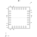
- Fig. 1 is a top view of a wiring board 1A in this embodiment.
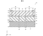
- Fig. 2 is a cross-sectional view taken along line II-II in Fig. 1.
- the X-axis direction shown in Fig. 1 will be described as the left-right direction
- the Y-axis direction as the front-rear direction
- the Z-axis direction as the up-down direction.
- the +X-axis direction in Fig. 1 will be described as the right direction
- the -X-axis direction as the left direction
- the +Z-axis direction as the upward direction
- the -Z-axis direction as the downward direction.
- the wiring board 1A includes a base body 10, a plurality of first connection terminals 21, a plurality of first external terminals 22, a plurality of first wiring conductors 30, a plurality of first conductors 35, a first metal body 41, a plurality of second conductors 42, a plurality of second connection terminals 23, a plurality of second external terminals 24, a plurality of second wiring conductors 50, a plurality of third conductors 55, a second metal body 61, a plurality of fourth conductors 62, and a frame body 70.
- the base 10 has a thickness in the vertical direction.
- the Z-axis direction may be referred to as the thickness direction.
- the base 10 may include a plurality of insulating layers stacked in the thickness direction. As shown in FIG. 2, the base 10 in this embodiment is constructed by stacking a first insulating layer 11, a second insulating layer 12, and a third insulating layer 13 from top to bottom.
- the first insulating layer 11, the second insulating layer 12, and the third insulating layer 13 are constructed of an insulating material. Examples of insulating materials that can be used include ceramics such as alumina and aluminum nitride, and resins.
- the upper surface of the first insulating layer 11 is the upper surface 14 of the base 10 as the first surface.
- the upper surface 14 of the base 10 may be a plane perpendicular to the thickness direction.
- the upper surface 14 of the base 10 functions as a first wiring layer.
- a plurality of first connection terminals 21 and a plurality of second connection terminals 23 are provided on the upper surface 14 of the base 10. In other words, the first connection terminals 21 and the second connection terminals 23 are located on the upper surface 14 of the base 10.
- the first connection terminals 21 and the second connection terminals 23 are terminals for electrically connecting to electrodes of an electronic component (not shown) mounted on the wiring board 1A.
- the first connection terminals 21 and the second connection terminals 23 may have a plating layer on their upper surfaces.
- some of the first connection terminals 21 are positioned on the top surface 14 of the base 10 at equal intervals along the front-to-rear direction, and other parts of the first connection terminals 21 are positioned on the top surface 14 of the base 10 at equal intervals along the left-to-right direction.
- the front-to-rear direction may be referred to as the first direction
- the left-to-right direction may be referred to as the second direction.
- the first connection terminal 21 and the second connection terminal 23 may be provided along the outer edge of the upper surface 14 of the base 10.
- the electronic component mounted on the wiring board 1A is an image sensor.
- a plurality of light receiving elements may be arranged as pixels in the center of the image sensor.
- a plurality of connection terminals to the wiring board may be arranged side by side on the outer edge of the image sensor.
- the first connection terminal 21 and the second connection terminal 23 are arranged side by side along the outer edge of the upper surface 14 of the base 10, thereby shortening the connection distance between the first connection terminal 21 and the second connection terminal 23 and the terminal on the image sensor side. This reduces the resistance of the wiring for connection.
- the connection is made by wire bonding, the occurrence of connection failure of the bonding wire is suppressed.
- the region between the first insulating layer 11 and the second insulating layer 12 functions as a second wiring layer 15
- the region between the second insulating layer 12 and the third insulating layer 13 functions as a third wiring layer 16.
- the lower surface of the third insulating layer 13 is the lower surface 17 of the base 10 as the second surface.
- the lower surface 17 of the base 10 may be a plane perpendicular to the thickness direction.
- the lower surface 17 of the base 10 is the surface opposite to the upper surface 14 of the base 10.
- the lower surface 17 faces the upper surface 14.
- the lower surface 17 of the base 10 functions as a fourth wiring layer.
- a plurality of first external terminals 22 and a plurality of second external terminals 24 are provided on the lower surface 17 of the base 10. In other words, the first external terminals 22 and the second external terminals 24 are located on the lower surface 17 of the base 10.
- the first external terminals 22 and the second external terminals 24 are terminals for electrically connecting to electrodes of an external device.
- the electrodes of the external device may be, for example, mounting electrodes of a printed circuit board.
- the first external terminal 22 and the second external terminal 24 may be located away from the outer edge of the lower surface 17 of the base 10, as shown in FIG. 5 described below. If the first external terminal 22 and the second external terminal 24 are located at the outer edge of the lower surface 17 of the base 10, the first external terminal 22 and the second external terminal 24 may come into contact with some external component, potentially causing a short circuit. In contrast, if the first external terminal 22 and the second external terminal 24 are located away from the outer edge of the lower surface 17 of the base 10, the first external terminal 22 and the second external terminal 24 are covered by the base 10, reducing the possibility of a short circuit occurring.
- each of the multiple first wiring conductors 30 connects the first connection terminal 21 and the first external terminal 22.
- each of the multiple first connection terminals 21 is connected to one of the multiple first external terminals 22 by the first wiring conductor 30.
- the connection between the first connection terminal 21 and the first external terminal 22 by the first wiring conductor 30 will be described with reference to FIG. 1 to FIG. 5.
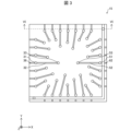
- FIG. 3 is a plan view showing the second wiring layer 15.
- FIG. 4 is a plan view showing the third wiring layer 16.
- FIG. 5 is a perspective view of the lower surface 17 of the base 10 viewed from above.
- the first wiring conductor 30 is located inside the base 10.
- the first wiring conductor 30 is conductive.
- the first wiring conductor 30 may be made of a metal with a high melting point, such as molybdenum or tungsten. This reduces the possibility of the first wiring conductor 30 melting when the base 10 is made of ceramic and the ceramic is heated to manufacture the wiring board 1A.
- the first wiring conductor 30 includes a first via conductor 31, a first interlayer conductor 32, and a second via conductor 33.
- the first via conductor 31 extends in a direction perpendicular to the upper surface 14 of the base 10. In other words, the first via conductor 31 extends in the thickness direction.
- the first via conductor 31 may be, for example, cylindrical in shape extending in the thickness direction.
- the first via conductor 31 is provided inside the first insulating layer 11. As shown in FIG. 2, the upper end of the first via conductor 31 is connected to the first connection terminal 21, and the lower end of the first via conductor 31 is connected to the first interlayer conductor 32. With this configuration, the first via conductor 31 electrically connects the first connection terminal 21 and the first interlayer conductor 32.
- the first interlayer conductor 32 may be provided on the second wiring layer 15, as shown in Figures 2 and 3. In this case, the first interlayer conductor 32 extends in a direction parallel to the upper surface 14 of the base 10. One end of the first interlayer conductor 32 is connected to the first via conductor 31, and the other end is connected to the second via conductor 33. With this configuration, the first interlayer conductor 32 electrically connects the first via conductor 31 and the second via conductor 33.
- the second via conductor 33 extends in a direction perpendicular to the upper surface 14 of the base 10. In other words, the second via conductor 33 extends in the thickness direction.
- the second via conductor 33 may be, for example, cylindrical in shape extending in the thickness direction.
- the second via conductor 33 is provided inside the second insulating layer 12 and inside the third insulating layer 13. As shown in FIG. 2 and FIG. 5, the upper end of the second via conductor 33 is connected to the first interlayer conductor 32, and the lower end of the second via conductor 33 is connected to the first external terminal 22. With this configuration, the second via conductor 33 electrically connects the first interlayer conductor 32 and the first external terminal 22.
- the first wiring conductor 30 has the first via conductor 31, the first interlayer conductor 32, and the second via conductor 33, which have the above-mentioned configuration, and electrically connects the first connection terminal 21 and the first external terminal 22.
- the first conductor 35 is a conductor used as an auxiliary conductor when forming a plating layer on the first connection terminal 21 by electrolytic plating.
- the first conductor 35 is connected to the first wiring conductor 30 and extends from the inside of the base 10 to the side surface 18.
- the side surface 18 is a surface extending from the upper surface 14 to the lower surface 17.
- the first conductor 35 has electrical conductivity.
- the first conductor 35 may be made of the same material as the material constituting the first wiring conductor 30, or may be made of a material different from the material constituting the first wiring conductor 30.
- the first conductor 35 may be provided in the second wiring layer 15 as shown in Figures 2 and 3.
- one end of the first conductor 35 is connected to the first via conductor 31 of the first wiring conductor 30, and the other end is exposed from the side surface 18 of the base 10.
- the width of the first conductor 35 may be smaller than the width of the first via conductor 31.
- the first conductor 35 is not used for electrical connection when using the wiring board 1A.
- the first metal body 41 is located independently of the first wiring conductor 30 inside the base 10. Here, independent means that the first metal body 41 and the first wiring conductor 30 are not electrically connected.
- the first metal body 41 has electrical conductivity.
- the first metal body 41 may be made of the same material as the material constituting the first wiring conductor 30, or may be made of a material different from the material constituting the first wiring conductor 30.
- the first metal body 41 may be provided in the third wiring layer 16 as shown in FIG. 2 and FIG. 4.
- the first metal body 41 has an L-shape consisting of a portion extending along the front-rear direction as the first portion and a portion extending along the left-right direction in a plan view.
- FIG. 4 the example shown in FIG.
- the portion of the first metal body 41 extending in the front-rear direction is located on the left outer edge of the third wiring layer 16, and the portion extending along the left-right direction is located on the upper outer edge of the third wiring layer 16.
- the first metal body 41 can be used for electrical connections such as ground connections.
- the second conductor 42 is connected to the first metal body 41 and extends from the inside of the base 10 to the side surface 18.
- the second conductor 42 is conductive.
- the second conductor 42 may be made of the same material as the material constituting the first wiring conductor 30, or may be made of a material different from the material constituting the first wiring conductor 30.
- the second conductor 42 may be provided in the third wiring layer 16 as shown in Figures 2 and 4. In this case, one end of the second conductor 42 is connected to the first metal body 41, and the other end is exposed from the side surface 18 of the base 10.
- the width of the second conductor 42 may be smaller than the width of the first metal body 41. In this embodiment, the second conductor 42 is not used for electrical connection when using the wiring board 1A.
- each of the multiple second wiring conductors 50 connects the second connection terminal 23 and the second external terminal 24.
- each of the multiple second connection terminals 23 is connected to one of the multiple second external terminals 24 by the second wiring conductor 50.
- the connection between the second connection terminal 23 and the second external terminal 24 by the second wiring conductor 50 will be described with reference to FIGS. 1 to 5.
- the second wiring conductor 50 is located inside the base 10.
- the second wiring conductor 50 is conductive.
- the material constituting the second wiring conductor 50 may be the same as the material constituting the first wiring conductor 30, or may be a material different from the material constituting the first wiring conductor 30.
- the second wiring conductor 50 includes a third via conductor 51, a second interlayer conductor 52, and a fourth via conductor 53.
- the third via conductor 51 extends in a direction perpendicular to the upper surface 14 of the base 10. In other words, the third via conductor 51 extends in the thickness direction.
- the third via conductor 51 may have the same shape as the first via conductor 31.
- the third via conductor 51 is provided inside the first insulating layer 11. The upper end of the third via conductor 51 is connected to the second connection terminal 23, and the lower end of the third via conductor 51 is connected to the second interlayer conductor 52. With this configuration, the third via conductor 51 electrically connects the second connection terminal 23 and the second interlayer conductor 52.
- the second interlayer conductor 52 may be provided in the second wiring layer 15, as shown in Figures 2 and 3. In this case, the second interlayer conductor 52 extends in a direction parallel to the upper surface 14 of the base 10. One end of the second interlayer conductor 52 is connected to the third via conductor 51, and the other end is connected to the fourth via conductor 53. With this configuration, the second interlayer conductor 52 electrically connects the third via conductor 51 and the fourth via conductor 53.
- the fourth via conductor 53 extends in a direction perpendicular to the upper surface 14 of the base 10. In other words, the fourth via conductor 53 extends in the thickness direction.
- the fourth via conductor 53 may have the same shape as the second via conductor 33.
- the fourth via conductor 53 is provided inside the second insulating layer 12 and inside the third insulating layer 13. As shown in Figures 2 and 5, the upper end of the fourth via conductor 53 is connected to the second interlayer conductor 52, and the lower end of the fourth via conductor 53 is connected to the second external terminal 24. With this configuration, the fourth via conductor 53 electrically connects the second interlayer conductor 52 and the second external terminal 24.
- the second wiring conductor 50 has the third via conductor 51, the second interlayer conductor 52, and the fourth via conductor 53, which have the above-mentioned configuration, and electrically connects the second connection terminal 23 and the second external terminal 24.
- the third conductor 55 is connected to the second wiring conductor 50 and extends from the inside of the base 10 to the side surface 18.
- the third conductor 55 is conductive.
- the third conductor 55 may be made of the same material as the material constituting the first wiring conductor 30, or may be made of a material different from the material constituting the first wiring conductor 30.
- the third conductor 55 may be provided in the third wiring layer 16 as shown in Figures 2 and 4. In this case, one end of the third conductor 55 is connected to the fourth via conductor 53 of the second wiring conductor 50, and the other end is exposed from the side surface 18 of the base 10.
- the end surface of the third conductor 55 exposed at the side surface 18 of the base 10 may be flush with the side surface 18 of the base 10.
- the second metal body 61 is located inside the base 10, independently of the first wiring conductor 30 and the first metal body 41.
- the second metal body 61 is conductive.
- the second metal body 61 may be made of the same material as the material constituting the first wiring conductor 30, or may be made of a material different from the material constituting the first wiring conductor 30.
- the second metal body 61 may be provided in the second wiring layer 15, as shown in FIG. 2 and FIG. 3.
- the second metal body 61 is L-shaped in plan view, consisting of a portion extending along the front-rear direction and a portion extending along the left-right direction as the second portion.
- the portion of the second metal body 61 extending along the front-rear direction is located on the right outer edge of the third wiring layer 16, and the portion extending along the left-right direction is located on the lower outer edge of the third wiring layer 16.
- the fourth conductor 62 is connected to the second metal body 61 and extends from the inside of the base 10 to the side surface 18.
- the fourth conductor 62 is conductive.
- the fourth conductor 62 may be made of the same material as the material constituting the first wiring conductor 30, or may be made of a material different from the material constituting the first wiring conductor 30.
- the fourth conductor 62 may be provided in the second wiring layer 15 as shown in Figures 2 and 3. In this case, one end of the fourth conductor 62 is connected to the second metal body 61, and the other end is exposed from the side surface 18 of the base 10.
- the end surface of the fourth conductor 62 exposed at the side surface 18 of the base 10 may be flush with the side surface 18 of the base 10.
- the fourth conductor 62 may be located on the same line as the first conductor 35. More specifically, the first conductor 35 may be located on an extension line of a virtual line on which the fourth conductor 62 extends from the second metal body 61. In the example shown in FIG. 2, the fourth conductor 62 is located on the same straight line extending in the X direction as the first conductor 35.
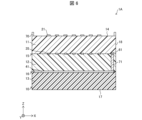
- connection conductor 71 is a cross-sectional view taken along the line VI-VI in FIG. 3. As shown in FIG. 6, the first metal body 41 and the second metal body 61 are electrically connected via a connection conductor 71.
- the connection conductor 71 includes a conductor extending in the thickness direction of the base 10.
- the connection conductor 71 may have the same shape as the first via conductor 31.
- the connection conductor 71 is formed in two places, the upper right and the lower left of the base 10, when viewed in a plan view from above, but this is not limited to this. Only one connection conductor 71 may be provided, or three or more connection conductors 71 may be provided.
- connection conductor 71 may extend from the second wiring layer 15 to the lower surface 17 of the base 10, and the connection conductor 71 may be exposed from the lower surface 17. Furthermore, for example, the connection conductor 71 exposed from the lower surface 17 may be connected to a metal index mark.
- the index mark may be used to check for the presence or absence of electrical leakage to the first metal body 41 and/or the second metal body 61 in the wiring board 1A.
- the index mark includes various configurations that are visible from the outside and are not used for electrical connection under normal use conditions, and may be a pattern used, for example, to determine whether or not a product is genuine by visual inspection, to check the installation orientation, etc.
- the frame body 70 may be located at the outer edge of the upper surface 14 of the base body 10.
- the frame body 70 defines the area in which electronic components are mounted on the wiring board 1A.
- the frame body 70 may be arranged so as to overlap at least a portion of the first conductor 35 when viewed from a plan view in the X-axis direction.
- the wiring board 1A is formed with the first conductors 35 used as auxiliary conductors when forming a plating layer on the first connection terminals 21 by electrolytic plating.
- the first conductors 35 are formed at regular intervals in the first and second directions in accordance with the arrangement of the first connection terminals 21. Therefore, when the distance between the first conductors 35 is the same as the wavelength of a signal such as a high-frequency signal, the first conductors 35 may receive an unnecessary signal. In this case, electromagnetic noise may occur in the signal transmission between the first connection terminals 21 and the first external terminals 22 and between the second connection terminals 23 and the second external terminals 24.
- the wiring board 1A has a first metal body 41 connected to a second conductor 42 that extends from the inside of the base 10 to the side surface 18.
- the first metal body 41 In order to allow the first metal body 41 to absorb electromagnetic noise more effectively, it is effective to make the first metal body 41 larger so that the potential of the first metal body 41 is closer to the ground potential.
- the first metal body 41 may have a band shape thicker than the second metal body 61. This makes it easier for the first metal body 41 to absorb electromagnetic noise, so that the influence of electromagnetic noise can be further reduced.
- the first metal body 41 can be formed in any shape in the area excluding the second via conductor 33, the fourth via conductor 53, and the third conductor 55 in the third wiring layer. Therefore, for example, the first metal body 41 may be formed in the entire area excluding the second via conductor 33, the fourth via conductor 53, and the third conductor 55 in the third wiring layer. This makes it easier for the first metal body 41 to absorb electromagnetic noise.
- some of the first connection terminals 21 are positioned side by side along the front-to-rear direction (first direction) in a plan view, and the first metal body 41 may have a first portion extending along the front-to-rear direction.
- the base 10 may include multiple insulating layers, a first insulating layer 11, a second insulating layer 12, and a third insulating layer 13, stacked in the thickness direction. This allows the space between the first insulating layer 11 and the second insulating layer 12, and the space between the second insulating layer 12 and the third insulating layer 13 to function as the second wiring layer 15 and the third wiring layer 16, respectively.
- each conductor such as the first metal body 41 and the first interlayer conductor 32, to be disposed in the second wiring layer 15 or the third wiring layer 16.
- the position of each conductor in the thickness direction can be limited, and in particular, the positional accuracy of each conductor in the thickness direction can be improved.
- the base 10 does not necessarily have to be composed of three insulating layers.
- the base 10 may be composed of two insulating layers.
- the first metal body 41 may be provided on the upper surface 14 of the base 10.
- the first metal body 41 may be covered with the same material as the material that constitutes the base 10.
- the first metal body 41 and the second conductor 42 do not need to be located at the same height in the thickness direction.
- the second conductor 42 connected by a via conductor extending in the thickness direction may be formed in a layer different from the layer in which the first metal body 41 is formed.
- the thickness of the base 10 can be made smaller than when the first metal body 41 and the second conductor 42 are located at different heights in the thickness direction.
- the length in the thickness direction of the second conductor 42 can be shortened.
- the first conductor 35 and the second conductor 42 do not need to be located at different heights in the thickness direction. However, if the first conductor 35 and the second conductor 42 are located at the same height in the thickness direction, they need to be designed so that they do not interfere with each other. In contrast, if the first conductor 35 and the second conductor 42 are located at different heights in the thickness direction, the first conductor 35 and the second conductor 42 do not interfere with each other, which improves the freedom of design.
- the wiring board 1A of one embodiment of the present disclosure does not necessarily have to include the multiple second connection terminals 23, the multiple second external terminals 24, the multiple second wiring conductors 50, the multiple third conductors 55, the second metal body 61, and the multiple fourth conductors 62, but including these components can improve the design freedom of the wiring board 1A.
- the first metal body 41 and the second metal body 61 do not need to be located at different heights in the thickness direction. However, by having the first metal body 41 and the second metal body 61 located at different heights in the thickness direction, it becomes easier for the second metal body 61 to absorb electromagnetic noise that could not be absorbed by the first metal body 41.
- the first metal body 41 and the second metal body 61 do not need to be connected via the connecting conductor 71.
- the metal body can be made larger, and the electric potential of the metal body is stabilized. This can improve the electromagnetic noise shielding performance.
- the second conductor 42 and the third conductor 55 do not need to be located at the same height in the thickness direction. However, by having the second conductor 42 and the third conductor 55 located at the same height in the thickness direction, the thickness of the base 10 can be reduced.
- the end faces of the first conductor 35 and the second conductor 42 do not need to be exposed on the side surface 18 of the base 10. However, since the end faces of the first conductor 35 and the second conductor 42 are exposed on the side surface 18 of the base 10, when a large number of first connection terminals 21 and second connection terminals 23 are obtained, they can be used as conductors for plating.
- the first interlayer conductor 32 is located on a different interlayer from the first metal body 41, and in a planar perspective, at least a portion of the first interlayer conductor 32 may overlap the first metal body 41. This makes it easier to control the electromagnetic shielding function of the first metal body 41, since the distance between the first metal body 41 and the ground can be adjusted by changing the depth.
- the wiring board 1A of the present disclosure it is not necessary for a portion of the base 10 to be located between adjacent first conductors 35. However, by having a portion of the base 10 located between adjacent first conductors 35, the adhesion between the layers constituting the base 10 can be improved.
- the frame body 70 may be arranged to overlap at least a portion of the first conductor 35 in a planar perspective. This increases the thickness of the wiring board 1A, thereby improving heat dissipation.
- first external terminal 22 and the second external terminal 24 are provided on the bottom surface 17 of the base 10, but this is not limited to the configuration. In one aspect of the wiring board of the present disclosure, the first external terminal 22 and the second external terminal 24 may be provided on the side surface 18 of the base 10.
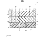
- FIG. 7 is a top view of the wiring board 1B in this embodiment.
- FIG. 8 is a cross-sectional view taken along line VIII-VIII in FIG. 1.
- FIG. 9 is a plan view showing the second wiring layer 15.
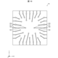
- FIG. 10 is a plan view showing the third wiring layer 16.
- FIG. 11 is a perspective view of the lower surface 17 of the base 10 as seen from above.
- the wiring board 1B includes a plurality of first connection terminals 21, a plurality of first external terminals 22, a plurality of first wiring conductors 130, a plurality of first conductors 135, a plurality of fifth conductors 136, a plurality of second connection terminals 23, a plurality of second external terminals 24, a plurality of second wiring conductors 150, a plurality of sixth conductors 156, a metal body 141 (first metal body), a plurality of second conductors 142, and a frame body 70.
- each of the multiple first wiring conductors 130 connects the first connection terminal 21 and the first external terminal 22.
- the connection between the first connection terminal 21 and the first external terminal 22 by the first wiring conductors 130 will be described with reference to FIGS. 7 to 11.
- the first wiring conductor 130 is located inside the base 10.
- the first wiring conductor 130 is conductive.
- the first wiring conductor 130 may be made of a metal with a high melting point, such as molybdenum or tungsten.
- the first wiring conductor 130 includes a first via conductor 131, a first interlayer conductor 132, and a second via conductor 133.
- the first via conductor 131 extends in a direction perpendicular to the upper surface 14 of the base 10.
- the first via conductor 131 is provided inside the first insulating layer 11 and inside the second insulating layer 12.
- the upper end of the first via conductor 131 is connected to the first connection terminal 21, and the lower end of the first via conductor 31 is connected to the first interlayer conductor 132.
- the first interlayer conductor 132 may be provided in the third wiring layer 16, as shown in Figures 8 and 10. In this case, the first interlayer conductor 132 extends in a direction parallel to the upper surface 14 of the base 10. One end of the first interlayer conductor 132 is connected to the first via conductor 131, and the other end is connected to the second via conductor 133.
- the second via conductor 133 extends in a direction perpendicular to the upper surface 14 of the base 10.
- the second via conductor 133 is provided inside the third insulating layer 13.
- the upper end of the second via conductor 133 is connected to the first interlayer conductor 132, and the lower end of the second via conductor 133 is connected to the first external terminal 22.
- the first wiring conductor 130 has the first via conductor 131, the first interlayer conductor 132, and the second via conductor 133, which have the above-mentioned configuration, and electrically connects the first connection terminal 21 and the first external terminal 22.
- the first conductor 135 is a conductor used as an auxiliary conductor when forming a plating layer on the first connection terminal 21 by electrolytic plating. As shown in FIG. 9, the first conductor 135 is connected to the first wiring conductor 130, has an L-shape, and extends from the inside of the base 10 to the side surface 18.
- the first conductor 135 is conductive.
- the first conductor 135 may be made of the same material as the material constituting the first wiring conductor 130, or may be made of a material different from the material constituting the first wiring conductor 130.
- the first conductor 135 may be provided in the second wiring layer 15 as shown in FIG. 8 and FIG. 9.
- one end of the first conductor 135 is connected to the first via conductor 131 of the first wiring conductor 130, and the other end is exposed from the side surface 18 of the base 10.
- the width of the first conductor 135 may be smaller than the width of the first via conductor 131.
- the first conductor 135 is not used for electrical connection when using the wiring board 1B.
- the fifth conductor 136 is a conductor used as an auxiliary conductor when forming a plating layer on the first connection terminal 21 by electrolytic plating.
- the fifth conductor 136 is connected to the first wiring conductor 130 and extends from the inside of the base 10 to the side surface 18.
- the fifth conductor 136 has electrical conductivity.
- the fifth conductor 136 may be made of the same material as the material constituting the first wiring conductor 130, or may be made of a material different from the material constituting the first wiring conductor 130.
- the fifth conductor 136 may be provided in the third wiring layer 16 as shown in FIG. 8 and FIG. 10.
- one end of the fifth conductor 136 is connected to the first via conductor 131 of the first wiring conductor 130, and the other end is exposed from the side surface 18 of the base 10.
- the width of the fifth conductor 136 may be smaller than the width of the first via conductor 131.
- the fifth conductor 136 is not used for electrical connection when using the wiring board 1B.
- each of the multiple second wiring conductors 150 connects the second connection terminal 23 and the second external terminal 24.
- the connection between the second connection terminal 23 and the second external terminal 24 by the second wiring conductors 150 will be described with reference to FIG. 7 to FIG. 11.
- the second wiring conductor 150 is located inside the base 10.
- the second wiring conductor 150 is conductive.
- the material constituting the second wiring conductor 150 may be the same as the material constituting the first wiring conductor 130, or may be a material different from the material constituting the first wiring conductor 130.
- the second wiring conductor 150 includes a third via conductor 151, a second interlayer conductor 152, and a fourth via conductor 153.
- the third via conductor 151 extends in a direction perpendicular to the upper surface 14 of the base 10.
- the third via conductor 151 is provided inside the first insulating layer 11 and inside the second insulating layer 12.
- the upper end of the third via conductor 151 is connected to the second connection terminal 23, and the lower end of the third via conductor 151 is connected to the second interlayer conductor 152.
- the second interlayer conductor 152 may be provided in the third wiring layer 16, as shown in Figures 8 and 10. In this case, the second interlayer conductor 152 extends in a direction parallel to the upper surface 14 of the base 10. One end of the second interlayer conductor 152 is connected to the third via conductor 151, and the other end is connected to the fourth via conductor 153.
- the fourth via conductor 153 extends in a direction perpendicular to the upper surface 14 of the base 10.
- the fourth via conductor 153 is provided inside the third insulating layer 13. As shown in Figures 8 and 11, the upper end of the fourth via conductor 153 is connected to the second interlayer conductor 152, and the lower end of the fourth via conductor 153 is connected to the second external terminal 24.
- the second wiring conductor 150 has the third via conductor 151, the second interlayer conductor 152, and the fourth via conductor 153, which have the above-mentioned configuration, and electrically connects the second connection terminal 23 and the second external terminal 24.
- the sixth conductor 156 is connected to the second wiring conductor 150 and extends from the inside of the base 10 to the side surface 18.
- the sixth conductor 156 is conductive.
- the sixth conductor 156 may be made of the same material as the material constituting the first wiring conductor 130, or may be made of a material different from the material constituting the first wiring conductor 130.
- the sixth conductor 156 may be provided in the third wiring layer 16, as shown in Figures 8 and 10. In this case, one end of the sixth conductor 156 is connected to the third via conductor 151 of the second wiring conductor 150, and the other end is exposed from the side surface 18 of the base 10.
- the metal body 141 is located independently of the first wiring conductor 130 inside the base 10. Here, independent means that the metal body 141 and the first wiring conductor 130 are not electrically connected.
- the metal body 141 has electrical conductivity.
- the metal body 141 may be made of the same material as the material constituting the first wiring conductor 130, or may be made of a material different from the material constituting the first wiring conductor 130.
- the metal body 141 may be provided in the second wiring layer 15 as shown in Figures 8 and 9.
- the metal body 141 is formed in a rectangular frame shape having a space inside.
- the metal body 141 is not limited to this shape, and may be formed, for example, in a circular frame shape, or may be formed as a rectangular metal plate without a space inside.
- the second conductor 142 is connected to the metal body 141 and extends from the inside of the base 10 to the side surface 18.
- the second conductor 142 is conductive.
- the second conductor 142 may be made of the same material as the material constituting the first wiring conductor 130, or may be made of a material different from the material constituting the first wiring conductor 130.
- the second conductor 142 may be provided in the second wiring layer 15 as shown in FIG. 9. In this case, one end of the second conductor 142 is connected to the metal body 141, and the other end is exposed from the side surface 18 of the base 10.
- the width of the second conductor 142 may be smaller than the width of the metal body 141. In this embodiment, the second conductor 142 is not used for electrical connection when using the wiring board 1B.
- the wiring board 1B is formed with the first conductors 135 used as auxiliary conductors when forming a plating layer by electrolytic plating on the first connection terminals 21.
- the first conductors 135 are formed at regular intervals corresponding to the arrangement of the first connection terminals 21. Therefore, if the distance between the first conductors 35 is the same as the wavelength of a signal such as a high-frequency signal, the first conductors 135 may receive an unnecessary signal. In this case, electromagnetic noise may be generated in the signal transmission between the first connection terminals 21 and the first external terminal 22, and in the signal transmission between the second connection terminals 23 and the second external terminal 24.
- the wiring board 1B has a metal body 141 connected to a second conductor 142 that extends from the inside of the base 10 to the side surface 18.
- wiring board 1B the only metal body to reduce the possibility of being affected by electromagnetic noise is metal body 141. This allows the thickness of base 10 to be reduced compared to wiring board 1A in embodiment 1, which includes multiple metal bodies located on different layers, and also makes connecting conductor 71 in embodiment 1 unnecessary.
- a wiring board comprises a base having a first surface, a second surface opposite to the first surface, and a side extending from the first surface toward the second surface, a plurality of first connection terminals located on the first surface, a plurality of first external terminals located on the second surface, a plurality of first wiring conductors located inside the base and connecting the first connection terminals and the first external terminals, a first conductor connected to each of the plurality of first wiring conductors and extending from the inside of the base to the side surface, a first metal body located inside the base independently of the first wiring conductors, and a second conductor connected to the first metal body and extending from the inside of the base to the side surface.
- the wiring board according to aspect 2 of the present disclosure may be the same as the above-mentioned aspect 1, in which at least some of the first connection terminals are aligned along a first direction in a plan view, and the first metal body has a first portion extending along the first direction.
- the wiring board according to aspect 3 of the present disclosure may be the wiring board according to aspect 1 or 2 above, in which the direction perpendicular to the first surface is the thickness direction, and the base may include a plurality of insulating layers stacked in the thickness direction.
- the direction perpendicular to the first surface may be the thickness direction, and the first metal body and the second conductor may be located at the same height in the thickness direction.
- the wiring board according to aspect 5 of the present disclosure may be any of aspects 1 to 4 above, in which the direction perpendicular to the first surface is the thickness direction, and the first conductor and the second conductor may be located at different heights in the thickness direction.
- the wiring board according to aspect 6 of the present disclosure may be any of aspects 1 to 5 above, in which the second surface is the surface opposite to the first surface, and the first external terminal is located away from the outer edge of the second surface.
- the wiring board according to aspect 7 of the present disclosure may further include, in any one of aspects 1 to 6 above, a plurality of second connection terminals located on the first surface, a plurality of second external terminals located on the second surface, a plurality of second wiring conductors located inside the base and connecting the second connection terminals and the second external terminals, a third conductor connected to each of the plurality of second wiring conductors and extending from inside the base to the side surface, a second metal body located inside the base independently of the first wiring conductors and the first metal body, and a fourth conductor connected to the second metal body and extending from inside the base to the side surface.
- the wiring board according to aspect 8 of the present disclosure is the same as the above-mentioned aspect 7, in which at least some of the second connection terminals are positioned along a second direction in a plan view, and the second metal body may have a second portion extending along the second direction.
- the wiring board according to aspect 9 of the present disclosure may be the same as in aspect 7 or 8 above, in that the direction perpendicular to the first surface is the thickness direction, and the first metal body and the second metal body may be located at different heights in the thickness direction.
- the wiring board according to aspect 10 of the present disclosure is any one of aspects 7 to 9 above, in which the first metal body and the second metal body may be connected via a connection conductor including a conductor extending in the thickness direction of the base.
- the wiring board according to aspect 11 of the present disclosure may be any of aspects 7 to 10 above, in which the direction perpendicular to the first surface is the thickness direction, and the second conductor and the third conductor are located at the same height in the thickness direction.
- the wiring board according to aspect 12 of the present disclosure is any one of aspects 1 to 11 above, in which the end faces of the first conductor and the second conductor may be exposed on the side surface.
- the wiring board according to aspect 13 of the present disclosure is the same as in aspect 3 above, in which the first wiring conductor includes a via conductor extending in a direction perpendicular to the first surface and an interlayer conductor extending in a direction parallel to the first surface, the interlayer conductor being located on a different layer from the first metal body, and at least a portion of the interlayer conductor overlapping the first metal body in a planar perspective view.
- the wiring board according to aspect 14 of the present disclosure may be any of aspects 1 to 13 above, in which the first metal body has a band shape that is thicker than the second conductor.
- the wiring board according to aspect 15 of the present disclosure may be any of aspects 1 to 14 above, in which a portion of the base is located between adjacent first conductors.
- the wiring board according to aspect 16 of the present disclosure may be any of aspects 1 to 15 above, in which the base has a frame body on the first surface, and the frame body may overlap at least a portion of the first conductor in a planar perspective view.
- the wiring board according to aspect 17 of the present disclosure is any one of aspects 1 to 16 above, in which the first connection terminal may have a plating layer.
- Reference Signs List 1A, 1B Wiring board 10 Base 11 First insulating layer 12 Second insulating layer 13 Third insulating layer 21 First connecting terminal 22 First external terminal 23 Second connecting terminal 24 Second external terminal 30, 130 First wiring conductor 31, 131 First via conductor 32, 132 First interlayer conductor 33, 133 Second via conductor 35, 135 First conductor 41 First metal body 42, 142 Second conductor 50, 150 Second wiring conductor 51, 151 Third via conductor 52, 152 Second interlayer conductor 53, 153 Fourth via conductor 55 Third conductor 61 Second metal body 62 Fourth conductor 70 Frame body 71 Connecting conductor 141 Metal body (first metal body)
Landscapes
- Engineering & Computer Science (AREA)
- Microelectronics & Electronic Packaging (AREA)
- Manufacturing & Machinery (AREA)
- Structure Of Printed Boards (AREA)
Priority Applications (2)
| Application Number | Priority Date | Filing Date | Title |
|---|---|---|---|
| JP2025510644A JPWO2024203720A1 (https=) | 2023-03-24 | 2024-03-21 | |
| CN202480019577.9A CN120883732A (zh) | 2023-03-24 | 2024-03-21 | 配线基板 |
Applications Claiming Priority (2)
| Application Number | Priority Date | Filing Date | Title |
|---|---|---|---|
| JP2023048831 | 2023-03-24 | ||
| JP2023-048831 | 2023-03-24 |
Publications (1)
| Publication Number | Publication Date |
|---|---|
| WO2024203720A1 true WO2024203720A1 (ja) | 2024-10-03 |
Family
ID=92906095
Family Applications (1)
| Application Number | Title | Priority Date | Filing Date |
|---|---|---|---|
| PCT/JP2024/011014 Ceased WO2024203720A1 (ja) | 2023-03-24 | 2024-03-21 | 配線基板 |
Country Status (3)
| Country | Link |
|---|---|
| JP (1) | JPWO2024203720A1 (https=) |
| CN (1) | CN120883732A (https=) |
| WO (1) | WO2024203720A1 (https=) |
Citations (4)
| Publication number | Priority date | Publication date | Assignee | Title |
|---|---|---|---|---|
| JP2017034054A (ja) * | 2015-07-31 | 2017-02-09 | 株式会社村田製作所 | セラミック配線基板、電子回路モジュールおよび電子回路モジュールの製造方法 |
| WO2017170535A1 (ja) * | 2016-03-31 | 2017-10-05 | 株式会社村田製作所 | 回路モジュール |
| JP2017191822A (ja) * | 2016-04-12 | 2017-10-19 | Tdk株式会社 | 電子回路パッケージ |
| US20230074430A1 (en) * | 2021-09-07 | 2023-03-09 | STATS ChipPAC Pte. Ltd. | Double-Sided Partial Molded SIP Module |
-
2024
- 2024-03-21 WO PCT/JP2024/011014 patent/WO2024203720A1/ja not_active Ceased
- 2024-03-21 CN CN202480019577.9A patent/CN120883732A/zh active Pending
- 2024-03-21 JP JP2025510644A patent/JPWO2024203720A1/ja active Pending
Patent Citations (4)
| Publication number | Priority date | Publication date | Assignee | Title |
|---|---|---|---|---|
| JP2017034054A (ja) * | 2015-07-31 | 2017-02-09 | 株式会社村田製作所 | セラミック配線基板、電子回路モジュールおよび電子回路モジュールの製造方法 |
| WO2017170535A1 (ja) * | 2016-03-31 | 2017-10-05 | 株式会社村田製作所 | 回路モジュール |
| JP2017191822A (ja) * | 2016-04-12 | 2017-10-19 | Tdk株式会社 | 電子回路パッケージ |
| US20230074430A1 (en) * | 2021-09-07 | 2023-03-09 | STATS ChipPAC Pte. Ltd. | Double-Sided Partial Molded SIP Module |
Also Published As
| Publication number | Publication date |
|---|---|
| CN120883732A (zh) | 2025-10-31 |
| JPWO2024203720A1 (https=) | 2024-10-03 |
Similar Documents
| Publication | Publication Date | Title |
|---|---|---|
| KR102266668B1 (ko) | 고주파 모듈 | |
| JPWO2017170535A1 (ja) | 回路モジュール | |
| US11716813B2 (en) | Module | |
| JPH065847A (ja) | 半導体パワーモジュール | |
| US12193144B2 (en) | Module | |
| JP2022168758A (ja) | フレキシブル配線板、モジュール、及び電子機器 | |
| US20220320752A1 (en) | Antenna module | |
| KR101555403B1 (ko) | 배선기판 | |
| US12101886B2 (en) | Electronic apparatus and substrate | |
| CN220233160U (zh) | 电路模块 | |
| WO2024203720A1 (ja) | 配線基板 | |
| JP6612008B1 (ja) | 電子機器 | |
| US12363821B2 (en) | Circuit module | |
| US11984637B2 (en) | Transmission line and electronic device | |
| WO2021049521A1 (ja) | モジュール | |
| JP7455730B2 (ja) | 配線基板 | |
| CN219626637U (zh) | 电路模块 | |
| WO2022215372A1 (ja) | 電子回路モジュール | |
| JP2023134096A (ja) | プリント基板および回路基板 | |
| US12622299B2 (en) | Electronic circuit module | |
| JP2017220505A (ja) | プリント基板 | |
| JP7827160B2 (ja) | アンテナモジュール | |
| CN110996501A (zh) | 具有贯穿式导电及散热部件的电路板和功率模组 | |
| US12446159B2 (en) | Electronic circuit module | |
| KR102736599B1 (ko) | 반도체 모듈 |
Legal Events
| Date | Code | Title | Description |
|---|---|---|---|
| 121 | Ep: the epo has been informed by wipo that ep was designated in this application |
Ref document number: 24779840 Country of ref document: EP Kind code of ref document: A1 |
|
| ENP | Entry into the national phase |
Ref document number: 2025510644 Country of ref document: JP Kind code of ref document: A |
|
| WWE | Wipo information: entry into national phase |
Ref document number: 2025510644 Country of ref document: JP |
|
| WWE | Wipo information: entry into national phase |
Ref document number: 202480019577.9 Country of ref document: CN |
|
| NENP | Non-entry into the national phase |
Ref country code: DE |
|
| WWP | Wipo information: published in national office |
Ref document number: 202480019577.9 Country of ref document: CN |
|
| 122 | Ep: pct application non-entry in european phase |
Ref document number: 24779840 Country of ref document: EP Kind code of ref document: A1 |