WO2024203387A1 - ダイシング用粘着テープ - Google Patents
ダイシング用粘着テープ Download PDFInfo
- Publication number
- WO2024203387A1 WO2024203387A1 PCT/JP2024/009977 JP2024009977W WO2024203387A1 WO 2024203387 A1 WO2024203387 A1 WO 2024203387A1 JP 2024009977 W JP2024009977 W JP 2024009977W WO 2024203387 A1 WO2024203387 A1 WO 2024203387A1
- Authority
- WO
- WIPO (PCT)
- Prior art keywords
- adhesive tape
- base film
- dicing
- adhesive
- wafer
- Prior art date
- Legal status (The legal status is an assumption and is not a legal conclusion. Google has not performed a legal analysis and makes no representation as to the accuracy of the status listed.)
- Ceased
Links
Images


Classifications
-
- H—ELECTRICITY
- H10—SEMICONDUCTOR DEVICES; ELECTRIC SOLID-STATE DEVICES NOT OTHERWISE PROVIDED FOR
- H10P—GENERIC PROCESSES OR APPARATUS FOR THE MANUFACTURE OR TREATMENT OF DEVICES COVERED BY CLASS H10
- H10P72/00—Handling or holding of wafers, substrates or devices during manufacture or treatment thereof
- H10P72/70—Handling or holding of wafers, substrates or devices during manufacture or treatment thereof for supporting or gripping
- H10P72/74—Handling or holding of wafers, substrates or devices during manufacture or treatment thereof for supporting or gripping using temporarily an auxiliary support
- H10P72/7402—Wafer tapes, e.g. grinding or dicing support tapes
-
- C—CHEMISTRY; METALLURGY
- C09—DYES; PAINTS; POLISHES; NATURAL RESINS; ADHESIVES; COMPOSITIONS NOT OTHERWISE PROVIDED FOR; APPLICATIONS OF MATERIALS NOT OTHERWISE PROVIDED FOR
- C09J—ADHESIVES; NON-MECHANICAL ASPECTS OF ADHESIVE PROCESSES IN GENERAL; ADHESIVE PROCESSES NOT PROVIDED FOR ELSEWHERE; USE OF MATERIALS AS ADHESIVES
- C09J7/00—Adhesives in the form of films or foils
- C09J7/20—Adhesives in the form of films or foils characterised by their carriers
- C09J7/22—Plastics; Metallised plastics
-
- C—CHEMISTRY; METALLURGY
- C09—DYES; PAINTS; POLISHES; NATURAL RESINS; ADHESIVES; COMPOSITIONS NOT OTHERWISE PROVIDED FOR; APPLICATIONS OF MATERIALS NOT OTHERWISE PROVIDED FOR
- C09J—ADHESIVES; NON-MECHANICAL ASPECTS OF ADHESIVE PROCESSES IN GENERAL; ADHESIVE PROCESSES NOT PROVIDED FOR ELSEWHERE; USE OF MATERIALS AS ADHESIVES
- C09J7/00—Adhesives in the form of films or foils
- C09J7/20—Adhesives in the form of films or foils characterised by their carriers
- C09J7/22—Plastics; Metallised plastics
- C09J7/24—Plastics; Metallised plastics based on macromolecular compounds obtained by reactions involving only carbon-to-carbon unsaturated bonds
-
- C—CHEMISTRY; METALLURGY
- C09—DYES; PAINTS; POLISHES; NATURAL RESINS; ADHESIVES; COMPOSITIONS NOT OTHERWISE PROVIDED FOR; APPLICATIONS OF MATERIALS NOT OTHERWISE PROVIDED FOR
- C09J—ADHESIVES; NON-MECHANICAL ASPECTS OF ADHESIVE PROCESSES IN GENERAL; ADHESIVE PROCESSES NOT PROVIDED FOR ELSEWHERE; USE OF MATERIALS AS ADHESIVES
- C09J7/00—Adhesives in the form of films or foils
- C09J7/20—Adhesives in the form of films or foils characterised by their carriers
- C09J7/29—Laminated material
-
- C—CHEMISTRY; METALLURGY
- C09—DYES; PAINTS; POLISHES; NATURAL RESINS; ADHESIVES; COMPOSITIONS NOT OTHERWISE PROVIDED FOR; APPLICATIONS OF MATERIALS NOT OTHERWISE PROVIDED FOR
- C09J—ADHESIVES; NON-MECHANICAL ASPECTS OF ADHESIVE PROCESSES IN GENERAL; ADHESIVE PROCESSES NOT PROVIDED FOR ELSEWHERE; USE OF MATERIALS AS ADHESIVES
- C09J7/00—Adhesives in the form of films or foils
- C09J7/30—Adhesives in the form of films or foils characterised by the adhesive composition
- C09J7/38—Pressure-sensitive adhesives [PSA]
-
- H—ELECTRICITY
- H10—SEMICONDUCTOR DEVICES; ELECTRIC SOLID-STATE DEVICES NOT OTHERWISE PROVIDED FOR
- H10P—GENERIC PROCESSES OR APPARATUS FOR THE MANUFACTURE OR TREATMENT OF DEVICES COVERED BY CLASS H10
- H10P95/00—Generic processes or apparatus for manufacture or treatments not covered by the other groups of this subclass
-
- C—CHEMISTRY; METALLURGY
- C09—DYES; PAINTS; POLISHES; NATURAL RESINS; ADHESIVES; COMPOSITIONS NOT OTHERWISE PROVIDED FOR; APPLICATIONS OF MATERIALS NOT OTHERWISE PROVIDED FOR
- C09J—ADHESIVES; NON-MECHANICAL ASPECTS OF ADHESIVE PROCESSES IN GENERAL; ADHESIVE PROCESSES NOT PROVIDED FOR ELSEWHERE; USE OF MATERIALS AS ADHESIVES
- C09J2203/00—Applications of adhesives in processes or use of adhesives in the form of films or foils
- C09J2203/326—Applications of adhesives in processes or use of adhesives in the form of films or foils for bonding electronic components such as wafers, chips or semiconductors
Definitions
- the present invention relates to an adhesive tape for dicing.
- the process of processing a semiconductor wafer or the like into a semiconductor chip and mounting it on a semiconductor device such as an integrated circuit (IC) includes various steps, such as a step of attaching a semiconductor wafer surface protective tape or a back-grind substrate to the patterned surface of the semiconductor wafer, a step of grinding the back surface of the semiconductor wafer to reduce its thickness, a step of mounting the thinned semiconductor wafer on an adhesive tape for dicing, a step of peeling off the semiconductor wafer surface protective tape or back-grind substrate from the semiconductor wafer, a step of dividing the semiconductor wafer by dicing, a pick-up step of picking up the divided semiconductor chips, a die bonding step of joining the picked-up semiconductor chips to a lead frame, and a molding step of sealing the semiconductor chips after the die bonding step with resin.
- steps such as a step of attaching a semiconductor wafer surface protective tape or a back-grind substrate to the patterned surface of the semiconductor wafer, a step of grinding the back surface of the
- the adhesive tape for dicing functions as a support for the semiconductor chip not only in the dicing step but also in the pick-up step.
- a method is known in which the dicing step is performed by laser irradiation. Specifically, a modified region that is the starting point of division is formed inside the semiconductor wafer by irradiating a laser from the dicing adhesive tape side, and then the modified region is divided by expanding the dicing adhesive tape to separate the semiconductor chips.
- This dicing method is called stealth dicing. In stealth dicing, in order to perform high-precision laser irradiation on the wafer and to enable visual inspection, etc., high transparency is required for the dicing adhesive tape.
- Patent Document 1 proposes a stealth dicing adhesive sheet having a substrate and an adhesive layer laminated on one side of the substrate, in which, when the substrate is pulled with a load of 0.2 g while being heated from 25° C. to 120° C. at a temperature increase rate of 20° C./min using a thermomechanical analyzer, the change in the substrate obtained by subtracting the initial length of the substrate from the length of the substrate at 60° C. is ⁇ L 60° C. , and the change in the substrate obtained by subtracting the initial length of the substrate from the length of the substrate at 90° C. is ⁇ L 90° C.
- the stealth dicing adhesive sheet satisfies the relationship of formula (1): ⁇ L 90° C. - ⁇ L 60° C.
- Patent Document 1 proposes a dicing sheet including a substrate and an adhesive layer laminated on a first surface of the substrate, the arithmetic mean roughness (Ra) of the second surface of the substrate being 0.01 ⁇ m or more and 0.5 ⁇ m or less, and the maximum height roughness (Rz) of the second surface of the substrate being 3 ⁇ m or less.
- This dicing sheet is said to have light transmittance suitable for high magnification imaging of a workpiece.
- flip chip connection is known as a method for mounting a semiconductor chip on a wiring board.
- a resin is filled between the semiconductor chip and the wiring board.
- the resin is made into an adhesive film such as NCF (Non Conductive Film), which is attached to the wafer before dicing and is singulated at the same time as the wafer.
- NCF Non Conductive Film
- the adhesive film is laminated to the surface of the wafer to which the dicing adhesive tape is not laminated. More specifically, this lamination is performed as follows. The laminate of the dicing adhesive tape and the wafer is placed on a chuck table (CT) heated to about 80° C.
- CT chuck table
- the dicing adhesive tape side is in contact with the chuck table, and fixed by vacuum adsorption.
- the adhesive film is laminated to the side of the wafer opposite to the dicing adhesive tape side.
- the above-mentioned decrease in transmittance is believed to be due to the fact that the unevenness of the surface of the chuck table is transferred to the dicing adhesive tape by vacuum suction at high temperatures, resulting in a rough back surface of the dicing adhesive tape.
- This problem can be improved by increasing the heat resistance (melting point, etc.) of the base film constituting the dicing adhesive tape.
- a highly heat-resistant material generally has high rigidity, and a dicing adhesive tape using a highly heat-resistant material has a problem of reduced expandability (elongation) of the dicing adhesive tape during expansion and cutting.
- the present invention was made in consideration of the problems with the conventional technology described above, and aims to provide an adhesive tape for dicing that exhibits sufficiently high transmittance to laser light even after being vacuum-attached to a chuck table under heating, and also has excellent expandability when expanded and cut.
- the inventors have found that the above problems can be solved by setting the penetration temperature at or above a specific temperature and controlling the surface roughness to or below a specific value, even when a resin with a low melting point is used for the base film of a dicing adhesive tape. That is, the above-mentioned object of the present invention is achieved by the following means.
- a dicing adhesive tape having an adhesive layer on a base film, wherein the melting point of the base film is 150°C or lower, the surface roughness Ra of a surface A of the base film opposite the adhesive layer is 0.10 ⁇ m or lower, and the penetration temperature of this surface A is 80°C or higher.
- the numerical range expressed using “to” means a range including the numerical values before and after “to” as the lower and upper limits.
- the term “(meth)acrylic” refers to either or both of acrylic and methacrylic. The same applies to (meth)acrylate.
- the MD direction is the flow direction during film formation
- the TD direction is the direction perpendicular to the MD direction.
- the adhesive tape for dicing of the present invention exhibits sufficiently high transmittance to laser light even after being vacuum-attached to a chuck table under heating, and also has excellent expandability when expanded and cut.
- FIG. 1 is a cross-sectional view showing one embodiment of the pressure-sensitive adhesive tape for dicing of the present invention.
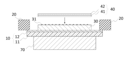
- FIG. 2 is a schematic vertical cross-sectional view showing an adhesive film laminating step in a preferred embodiment of a method for manufacturing a semiconductor device using the adhesive tape for dicing of the present invention.
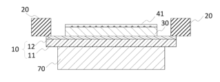
- FIG. 3 is a schematic vertical cross-sectional view showing a state after the release film has been peeled off in a preferred embodiment of the method for producing a semiconductor device using the adhesive tape for dicing of the present invention.
- FIG. 4 is a schematic vertical cross-sectional view showing a state after the wafer is removed from the chuck table in a preferred embodiment of the method for manufacturing a semiconductor device using the adhesive tape for dicing of the present invention.
- FIG. 1 is a cross-sectional view showing one embodiment of the pressure-sensitive adhesive tape for dicing of the present invention.
- FIG. 2 is a schematic vertical cross-sectional view showing an adhesive film laminating step in a preferred embodiment
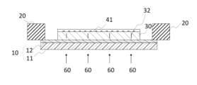
- FIG. 5 is a schematic vertical cross-sectional view showing a modified region forming step in a preferred embodiment of a method for manufacturing a semiconductor device using the adhesive tape for dicing of the present invention.
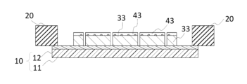
- FIG. 6 is a schematic vertical cross-sectional view showing a state after heat shrinking in a preferred embodiment of a method for manufacturing a semiconductor device using the adhesive tape for dicing of the present invention.
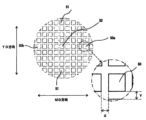
- FIG. 2 is an explanatory diagram showing measurement points of kerf width in the evaluation of Examples and Comparative Examples.
- the pressure-sensitive adhesive tape for dicing of the present invention (hereinafter also referred to as "the pressure-sensitive adhesive tape of the present invention") has a base film and a pressure-sensitive adhesive layer.
- the pressure-sensitive adhesive tape of the present invention is used as a so-called dicing film.
- the pressure-sensitive adhesive tape of the present invention is suitable as a pressure-sensitive adhesive tape for stealth dicing having expandability and heat shrinkability.
- the base film has a melting point of 150° C. or less as measured by differential scanning calorimetry (DSC).
- the base film has a surface roughness Ra of 0.10 ⁇ m or less on the surface opposite to the pressure-sensitive adhesive layer.
- the penetration temperature of the opposite surface is 80° C. or more.
- the adhesive tape of the present invention is unlikely to transfer the unevenness of the chuck table surface even when heated (e.g., heated for several minutes at a temperature of 80° C. or higher) when adhering the adhesive film to a semiconductor wafer (hereinafter, also simply referred to as "wafer") before dicing, so that the laser light transmittance can be sufficiently maintained even after vacuum adsorption to the chuck table under heating, and as a result, the modified region can be formed with high accuracy by laser irradiation from the adhesive tape side.
- it has excellent expandability in the expansion process after dicing, and the efficiency of dividing the wafer into wafer chips (semiconductor chips) can be further improved.
- more uniform heat shrinkage is possible during heat shrinking, making it easier to set the kerf width within an appropriate range in the MD and TD directions.
- FIG. 1 is a cross-sectional view showing one embodiment of the pressure-sensitive adhesive tape 10 according to the present invention.
- the pressure-sensitive adhesive tape 10 of the present invention has a base film 11 and a pressure-sensitive adhesive layer 12.
- the pressure-sensitive adhesive layer 12 may be pre-cut into a predetermined shape in accordance with the process or device used.
- the pressure-sensitive adhesive tape 10 of the present invention may be in a form cut into pieces each corresponding to a single wafer, or may be in a form in which a long sheet formed with a plurality of pieces cut into pieces each corresponding to a single wafer is wound into a roll.
- the pressure-sensitive adhesive layer means a coating layer of a pressure-sensitive adhesive composition, and is in a state in which the polymer contained in the pressure-sensitive adhesive exerts adhesive or cohesive force.
- the pressure-sensitive adhesive layer is energy ray-curable, the pressure-sensitive adhesive layer is in a state before being cured by energy ray irradiation.
- the base film 11 may be a single layer or a laminate of multiple layers. In the case of a laminate, it is preferable that each layer is made of a different material.
- the base film 11 has a melting point of 150° C. or lower.
- the melting point is preferably 140° C. or less, more preferably 130° C. or less, more preferably 120° C. or less, more preferably 110° C. or less, even more preferably 100° C. or less, and particularly preferably 90° C. or less.
- the preferred range of the melting point of the base film 11 is preferably 50 to 150° C., more preferably 50 to 140° C., even more preferably 50 to 130° C., even more preferably 60 to 120° C., even more preferably 60 to 110° C., even more preferably 70 to 100° C., and even more preferably 70 to 90° C.
- the melting point of the base film 11 can be measured by differential scanning calorimetry (DSC) using the method described in the Examples.
- DSC differential scanning calorimetry
- the melting point of the base film 11 can be adjusted to the above range by controlling the material, layer structure, and blending with other materials of the base film 11 .
- the surface roughness (arithmetic mean roughness) Ra of the surface of the base film 11 opposite to the surface on which the pressure-sensitive adhesive layer 12 is formed (hereinafter sometimes referred to as the "back surface") is 0.10 ⁇ m or less, preferably 0.08 ⁇ m or less, more preferably 0.06 ⁇ m or less, and even more preferably 0.04 ⁇ m or less.
- the lower limit of the surface roughness Ra of the back surface is not particularly limited, but 0.01 ⁇ m or more is practical. Therefore, the preferred range of Ra of the back surface of the base film 11 is preferably 0.01 to 0.10 ⁇ m, more preferably 0.01 to 0.08 ⁇ m, even more preferably 0.01 to 0.06 ⁇ m, and even more preferably 0.01 to 0.04 ⁇ m.
- the surface roughness Ra of the outermost layer on the back surface side of the base film 11 is within the above range.
- the surface roughness Ra of the back surface of the base film 11 can be controlled by the preparation method of the base film 11. For example, in the case of the T-die method and the calendar method, it can be controlled by adjusting the surface roughness of the cooling roll during film extrusion, and in the case of the solution casting method, it can be controlled by adjusting the surface roughness of the drum or belt.
- the surface roughness Ra of the surface of the base film 11 on which the pressure-sensitive adhesive layer 12 is formed is not particularly limited.
- the surface roughness Ra of the base film 11 can be measured in accordance with JIS B0601:2001 by the method described in the Examples.
- the penetration temperature of the back surface of the base film 11 is 80° C. or higher, preferably 83° C. or higher, more preferably 85° C. or higher, more preferably 88° C. or higher, even more preferably 90° C. or higher, and particularly preferably 92° C. or higher.
- the upper limit of the penetration temperature of the back surface of the base film 11 is preferably 100° C. or lower, more preferably 98° C. or lower, and even more preferably 95° C. or lower.
- the preferred range of the penetration temperature of the back surface of the base film 11 is preferably 80 to 100° C., more preferably 83 to 98° C., even more preferably 85 to 98° C., even more preferably 88 to 98° C., even more preferably 90 to 95° C., and particularly preferably 92 to 95° C.
- the penetration temperature can be measured in accordance with JIS K7196:2012 by thermomechanical analysis (TMA) using a method described in the Examples.
- TMA thermomechanical analysis
- the penetration temperature can be controlled by selecting the material constituting the base film, forming the base film by laminating a plurality of layers of different materials, controlling the thickness of the resin layer constituting the laminate, etc.
- the penetration temperature tends to be high.
- the penetration temperature tends to be high.
- the penetration temperature tends to be high.
- the penetration temperature tends to be low.
- the penetration temperature of the back surface of the base film 11 is 80°C or higher, even if a material having a relatively low melting point and not very high rigidity is used as the constituent material of the base film, it is possible to effectively prevent the unevenness of the chuck table surface from being transferred to the base film by vacuum suction at high temperatures, for example.
- the relationship between the needle penetration temperature (T1) of the surface on which the adhesive layer 12 is formed and the needle penetration temperature (T2) of the surface on which the adhesive layer 12 is not formed (rear surface) is [(T2)-(T1)]>0°C (i.e., T2>T1).
- T1 and T2 are more preferably [(T2)-(T1)]>20°C, more preferably [(T2)-(T1)]>30°C, even more preferably [(T2)-(T1)]>40°C, and particularly preferably [(T2)-(T1)]>50°C.
- T1 and T2 can also be [(T2)-(T1)]>80°C. There is no particular upper limit to [(T2)-(T1)], but 100°C is practical. Therefore, the relationship between T1 and T2 is preferably 100°C > [(T2) - (T1)] > 0°C, more preferably 100°C > [(T2) - (T1)] > 20°C, even more preferably 100°C > [(T2) - (T1)] > 30°C, even more preferably 100°C > [(T2) - (T1)] > 40°C, and even more preferably 100°C > [(T2) - (T1)] > 50°C.
- the base film 11 does not have a yield point between 0% and 50% elongation in the stress-elongation curve at ⁇ 15° C.
- a yield point can be determined by the method described in the Examples.
- the above stress-strain curve is a curve obtained by elongation in the TD direction.
- the absolute value of the difference between the stress (MD stress, S1) (MPa) when elongated in the MD direction at an elongation rate of 30% and the stress (TD stress, S2) (MPa) when elongated in the TD direction at an elongation rate of 30% is 4 MPa or less (satisfying 4 MPa ⁇
- the material of the base film 11 is not particularly limited as long as it can achieve the above melting point, surface roughness Ra, and penetration temperature. It is preferable that the base film 11 has uniform and isotropic expandability, since this allows the wafer to be cut evenly in all directions during the expanding step. From these viewpoints, the material of the base film 11 is preferably selected from polyolefin resins and polyvinyl chloride resins.
- the above polyolefin resins include polyethylene, polypropylene, ethylene-propylene copolymers, polybutene-1, poly-4-methylpentene-1, ethylene-vinyl acetate copolymers, ethylene-(meth)acrylic acid alkyl ester copolymers (ethylene-ethyl acrylate copolymers, ethylene-methyl acrylate copolymers, ethylene-methyl methacrylate copolymers, etc.), ethylene-acrylic acid copolymers, ionomers, and other ⁇ -olefin homopolymer or copolymer resins, or mixtures of these.
- ionomer resins which are synthetic resins that utilize the cohesive force of metal ions to form polymer aggregates
- examples thereof include ionomer resins in which an ethylene-(meth)acrylic acid binary copolymer or an ethylene-(meth)acrylic acid-(meth)acrylic acid alkyl ester terpolymer is crosslinked with a metal ion.
- the metal ions contained in the ionomer resins are not particularly limited, but examples include zinc ions and sodium ions. Zinc ions are preferred in terms of low elution and low contamination.
- ionomer resins have a greater restoring force against tension than resins without metal ions, and experience a greater shrinkage stress when heat is applied to the stretched state after the expanding step. Therefore, ionomer resins are preferable in that they can be used in a heat shrink step in which the slack generated in the tape after the expanding step is removed by thermal shrinkage and the tape is tensioned to stably maintain the spacing between the individual wafer chips.
- thermoplastic crosslinked resins obtained by crosslinking a resin selected from low-density polyethylene having a specific gravity of 0.910 or more and less than 0.930, ultra-low-density polyethylene having a specific gravity of less than 0.910, and ethylene-vinyl acetate copolymer are also suitable.
- a method of crosslinking a method of irradiating the resin with energy rays such as electron beams can be mentioned.
- Such a thermoplastic crosslinked resin has a certain degree of uniform extensibility because crosslinked and non-crosslinked sites coexist in the resin.
- thermoplastic crosslinked resin contains almost no chlorine atoms in the molecular chain structure, so that even if the tape that is no longer needed after use is incinerated, it does not generate chlorinated aromatic hydrocarbons such as dioxins and their analogues, and the environmental load is small.
- the base film 11 is a single layer, but is not limited thereto and may be a multi-layer.
- the multi-layer may be a multi-layer in which two or more layers made of different resins are laminated, or a multi-layer in which layers made of one type of resin are laminated. If the two or more resins are crosslinked resins or non-crosslinked resins, it is preferable from the viewpoint that the properties of each of them are enhanced and expressed, and if a crosslinked resin and a non-crosslinked resin are combined and laminated, it is preferable from the viewpoint that the shortcomings of each of them are compensated for.
- the multi-layered base film 11 can be produced by a conventional extrusion method, lamination method, etc. When a lamination method is used, an adhesive may be interposed between the layers. A conventional adhesive can be used as the adhesive.
- the base film 11 preferably contains at least one of an ethylene-(meth)acrylic acid alkyl ester copolymer resin and an ionomer resin. It is also preferable that the base film 11 is a laminate in which a layer containing an ethylene-(meth)acrylic acid alkyl ester copolymer resin and a layer containing an ionomer resin are laminated.
- the thickness of the base film 11 is not particularly limited, but is preferably 50 to 200 ⁇ m, more preferably 70 to 160 ⁇ m, even more preferably 100 to 150 ⁇ m, even more preferably 100 to 140 ⁇ m, and even more preferably 100 to 120 ⁇ m.
- the adhesive layer 12 constituting the adhesive tape 10 of the present invention is not particularly limited as long as it has a retention property sufficient to prevent peeling from the wafer during the dicing process, a property of transmitting stress due to expansion to the modified area of the wafer, and a property that allows peeling from the wafer chip during pick-up.
- the adhesive constituting the adhesive layer 12 is not particularly limited as long as it exhibits the above-mentioned characteristics, and an energy ray curable adhesive is preferable. If an energy ray curable adhesive is used, picking up becomes easy by curing it before the pick-up step.
- the energy ray refers to light rays such as ultraviolet rays, or ionizing radiation such as electron beams.
- a normal adhesive used as an adhesive for a dicing adhesive tape can be used without any particular limitation.
- the components, characteristics, and manufacturing method of the adhesive reference can be made to, for example, the descriptions in paragraphs [0039] to [0076] of Japanese Patent No. 6928852, paragraphs [0033] to [0052] of Japanese Patent No. 6989561, and paragraphs [0031] to [0057] of JP-A-2023-13022.
- the adhesive constituting the adhesive layer 12 is preferably an acrylic adhesive containing a (meth)acrylic resin as a base polymer, and more preferably an acrylic adhesive containing an alkyl (meth)acrylate ester as a constituent.
- the alkyl (meth)acrylate ester preferably further has a radiation-curable group introduced into the side chain, and more preferably has a (meth)acrylic ester having an isocyanate group added thereto.
- the adhesive may further contain a radiation-curable oligomer, for example, a urethane (meth)acrylate oligomer.
- the thickness of the adhesive layer 12 is preferably 2 to 35 ⁇ m, more preferably 5 to 35 ⁇ m, even more preferably 5 to 30 ⁇ m, and even more preferably 10 to 30 ⁇ m.
- the adhesive tape 10 of the present invention is suitable for use in a manufacturing method of a semiconductor device including at least an adhesive film laminating step including fixing the adhesive tape 10 on a heated chuck table by vacuum suction, a modified area forming step of forming a modified area in a wafer by irradiating a laser beam from the adhesive tape side, and an expanding step of dividing the wafer by expanding. Therefore, the other steps and the order of the steps are not particularly limited.
- the adhesive tape 10 can be suitable for use in the following manufacturing method of a semiconductor device (A).
- Manufacturing method of semiconductor device (A) (a) bonding a backgrind substrate to a wafer surface on which a circuit pattern is formed; (b) a back grinding step of grinding the back surface of the wafer; (c) applying the adhesive tape of the present invention to the rear surface of the wafer and fixing the same to a ring frame; (d) peeling the back-grind substrate from the wafer; (e) an adhesive film laminating step of fixing the adhesive tape of the present invention, to which the wafer has been laminated, on a heated chuck table by vacuum adsorption from the base film side of the adhesive tape, and laminating an adhesive film to the surface of the wafer opposite to the adhesive tape; (f) a modified region forming step of irradiating a laser beam from the adhesive tape side onto a portion of the wafer to be divided to form a modified region inside the wafer by multiphoton absorption; (g) an expanding step of expanding the adhesive tape to divide the wafer and the adhesive film along the dividing lines to obtain a pluralit
- a backgrind substrate is attached to the front surface of the wafer 30 on which the circuit pattern 31 is formed (step (a)), and then a backgrind process is carried out to grind the rear surface of the wafer 30 (step (b)) (not shown).
- the backgrind substrate may be a normal backgrind substrate, and may be, for example, a glass substrate.
- the pressure-sensitive adhesive tape 10 of the present invention is laminated to the back surface of the wafer 30, and is further adhered and fixed to the ring frame 20 (step (c)).
- the pressure-sensitive adhesive layer 12 of the pressure-sensitive adhesive tape 10 of the present invention is disposed so as to contact the back surface of the wafer 30, and the ring frame 20 is disposed around the wafer 30 in the portion where the pressure-sensitive adhesive layer 12 is exposed.
- the back-grind substrate (not shown) is peeled off from the wafer 30 (step (d)).
- the pressure-sensitive adhesive tape 10 of the present invention having the wafer 30 attached thereto is fixed onto a heated chuck table 70 by vacuum adsorption from the base film 11 side, while an adhesive film 40 with a release film, consisting of an adhesive film 41 and a release film 42, is attached to the surface of the wafer 30 (step e).
- the heating temperature of the chuck table 70 at this time can be set to 80° C. or higher, taking into consideration the bonding with an adhesive film such as NCF.
- the release film 42 is peeled off from the adhesive film 41.
- Figure 3 shows the state after the release film 42 has been peeled off.
- the wafer 30 to which the adhesive tape 10 has been attached is removed from the chuck table 70.
- the unevenness of the surface of the chuck table is transferred to the back surface of the base film 11, resulting in a reduced transmittance of the laser light.
- the adhesive tape 10 of the present invention is used, this transfer can be effectively suppressed, and the transmittance of the laser light can be sufficiently maintained.
- the portion of the wafer 30 to be divided is irradiated with laser light 60 from the adhesive tape 10 side to form modified regions 32 inside the wafer 30 by multiphoton absorption (step (f)).
- the modified regions 32 are formed intermittently in four places.
- the pressure-sensitive adhesive tape 10 of the present invention with the wafer 30 and the ring frame 20 bonded together is placed on the stage of an expanding device with the base film 11 side facing down.
- the hollow cylindrical push-up member of the expansion device is raised to expand (expand) the adhesive tape 10 (step (g)).
- the expansion conditions are, for example, an expansion speed of 5 to 500 mm/sec and an expansion amount (push-up amount) of 5 to 25 mm.
- the adhesive film 41 is not broken at the portion bonded to the wafer 30 because the stretch (deformation) due to the expansion is suppressed, but at the position between the chips 33, the tension due to the expansion of the film is concentrated and the adhesive film 41 is broken. Therefore, the adhesive film 41 is also divided together with the wafer 30. As a result, a plurality of chips 33 with adhesive film pieces 43 attached thereto can be obtained, as shown in FIG. 6.
- step (h) hot air at 40 to 120°C is applied using a hot air nozzle to the annular heat-shrinkage area between the area of the adhesive tape 10 where the chips 33 are present and the ring frame 20, causing the base film 11 to heat shrink and restore the adhesive tape 10 to its taut state (step (h)).
- step (h) hot air at 40 to 120°C is applied using a hot air nozzle to the annular heat-shrinkage area between the area of the adhesive tape 10 where the chips 33 are present and the ring frame 20, causing the base film 11 to heat shrink and restore the adhesive tape 10 to its taut state.
- step (h) the adhesive layer 12 is subjected to an energy ray curing process or a heat curing process, etc., to weaken the adhesive force of the adhesive layer 12 to the chips 33, and then the chips 33 are picked up (step (i)).
- Base resin A 2-methacryloyloxyethyl isocyanate was added to an acrylic copolymer (glass transition temperature: -65°C) whose constituent units were 70% by mass of 2-ethylhexyl acrylate, 29% by mass of 2-hydroxyethyl acrylate, and 1% by mass of methacrylic acid, so that the double bond amount was 0.9 (meq/g).
- 0.3 parts by mass of a urethane acrylate oligomer having a weight average molecular weight of 850 was added to 100 parts by mass of this acrylic copolymer to obtain base resin A.
- Photopolymerization initiator Irgacure 184 (product name, manufactured by Ciba-Geigy Japan Ltd.)
- Hardener Coronate L (isocyanate hardener, product name, manufactured by Tosoh Corporation)
- Surface modifier TEGORad2200N (product name, manufactured by Tego Chemie Co., Ltd.)
- EMMA Ethylene-methyl methacrylate copolymer (AN4214C (product name), manufactured by Dow Mitsui Polychemicals)
- ION (1) Ionomer (Himilan 1855 (product name), manufactured by Dow Mitsui Polychemicals)
- ION (2) Ionomer (Himilan 1652 (product name), manufactured by Mitsui-Dow Polychemicals)
- ION (3) Ionomer (Himilan AM7326 (product name), manufactured by Dow Mitsui Polychemicals)
- PP Polypropylene (F724P (product name), manufactured by Prime Polymer Co., Ltd.)
- Substrate Film 1 Preparation of Substrate Film (Substrate Film 1) EMMA was melt-kneaded at 220°C in a multi-layer T-die extruder, extruded onto a metal roll (hereinafter also referred to as "mirror roll (1)") with one side mirror-finished. In this way, a base film 1 having a thickness of 100 ⁇ m was formed on the mirror roll (1). The surface shape of the metal roll was transferred to the surface of the base film 1 on the mirror roll (1). The surface roughness Ra of the surface of the obtained base film 1 on the mirror roll (1) side was 0.03 ⁇ m.
- Substrate film 2 was prepared in the same manner as in preparation of substrate film 1, except that mirror surface roll (2) was used instead of mirror surface roll (1).
- Substrate film 3 was prepared in the same manner as in the preparation of substrate film 1, except that ION (3) was used instead of EMMA.
- Base film 4 In the preparation of the base film 1, ION (1) and EMMA were co-extruded in a multilayer T-die extruder instead of EMMA, so that EMMA was on the mirror roll (1) side, to prepare a base film 4 having an ION (1) layer and an EMMA layer with a total thickness of 100 ⁇ m.
- the ION (1) and EMMA layers were 50% by mass and 50% by mass, respectively, of the total amount of the resin components in the base film 4.
- the ION (1) layer had a thickness of 50 ⁇ m
- the EMMA layer had a thickness of 50 ⁇ m.
- Substrate film 5 was prepared in the same manner as substrate film 4, except that the amounts of ION (1) and EMMA in the total amount of resin components of the substrate film were 20 mass% for ION (1) and 80 mass% for the EMMA layer.
- the ION (1) layer had a thickness of 20 ⁇ m
- the EMMA layer had a thickness of 80 ⁇ m.
- Substrate film 6 was prepared in the same manner as substrate film 5, except that the total thickness was 150 ⁇ m.
- the ION (1) layer had a thickness of 30 ⁇ m, and the EMMA layer had a thickness of 120 ⁇ m.
- Substrate film 7 was prepared in the same manner as in the preparation of substrate film 1, except that PP was used instead of EMMA.
- Substrate film 8 was prepared in the same manner as in the preparation of substrate film 1, except that ION(1) was used instead of EMMA.
- Substrate film 9 was prepared in the same manner as in the preparation of substrate film 1, except that ION(2) was used instead of EMMA.
- Substrate film 10 A substrate film 10 having an EMMA layer and an ION (1) layer and a total thickness of 100 ⁇ m was prepared in the same manner as the substrate film 1, except that in the preparation of the substrate film 1, EMMA and ION (1) were co-extruded instead of EMMA so that ION (1) was on the mirror roll (1) side.
- EMMA was 50 mass% and ION (1) was 50 mass%.
- the EMMA layer had a thickness of 50 ⁇ m
- the ION (1) layer had a thickness of 50 ⁇ m.
- Substrate film 11 was prepared in the same manner as in the preparation of substrate film 1, except that the textured roll (1) was used instead of the mirror-finished roll (1).
- Substrate film 12 was prepared in the same manner as in the preparation of substrate film 1, except that the textured roll (2) was used instead of the mirror-finished roll (1).
- the melting point, surface roughness Ra, and penetration temperature of each base film used in each adhesive tape in the Examples and Comparative Examples were measured as follows.
- melting point of base film The melting point of the base film was determined by measuring the melting peak temperature according to the DSC method (JIS K 7121:2001). The base films 1 to 12 obtained above were used as samples. When multiple melting peaks were observed, the temperature of the lowest melting peak was taken as the melting point.
- the penetration temperature was also measured on the surface (front surface) of the base film on which the pressure-sensitive adhesive layer was formed for the multi-layered base films 4 to 6 and 10.
- the pressure-sensitive adhesive tape was formed and measured in the same manner as in 3) Preparation of pressure-sensitive adhesive tape, except that the pressure-sensitive adhesive layer was formed on the back surface of the base film.
- the penetration temperature (T2) of the back surface of the base film is shown in the "Penetration temperature of base film” column in Table 1, and the difference ((T2)-(T1)) between the penetration temperature (T2) of the back surface of the base film and the penetration temperature (T1) of the front surface of the base film is shown in the "Penetration temperature difference (T2)-(T1) (°C)" column in Table 1.
- "-" indicates that no measurement was performed.
- the surface roughness Ra of the back surface of the base film was measured by attaching and fixing the adhesive layer of each of the adhesive tapes obtained above to a smooth silicon mirror wafer, measuring at any five points (approximately 5 mm in length x 5 points) on the back surface of the base film, and averaging the measured value to obtain the surface roughness Ra of the back surface.
- the measurement was performed using a measuring device: "Surftest SJ-310" (manufactured by Mitutoyo Corporation) according to JIS B0601.
- the measurement conditions were as follows: - Measurement conditions - Curve: R Parameters: 2 Filter: GAUSS ⁇ c: 0.8 mm ⁇ s: 2.5 ⁇ m Number of sections: 5
- - Measurement conditions - Measurement temperature: -15°C Use a low-temperature thermostatic chamber, place the sample, and start measurement 5 minutes after the temperature reaches -15°C.
- Distance between chucks 20 mm
- Tensile speed 300 mm/min
- Test piece A a test piece with a width of 5 mm in the MD direction and a length of 60 mm in the TD direction.
- Test piece B a test piece with a width of 5 mm in the TD direction and a length of 60 mm in the MD direction.
- the stress value of test piece A was defined as the TD stress (S2), and the stress of test piece B was defined as the MD stress (S1), and S1-S2 was calculated.
- the adhesive tapes of the Examples and Comparative Examples were evaluated for transmittance after heat adsorption, meandering of the modified area during stealth dicing, tape breakage during cool expansion, and kerf width as follows.
- each of the adhesive tapes obtained in the Examples and Comparative Examples was attached to a ring frame (inner diameter: 350 mm). Then, each of the adhesive tapes was attached to a porous chuck table (Porous Chuck (product name), Yoshioka Co., Ltd.) heated to 80° C. The wafer was placed on a 12-inch wafer (manufactured by Seikosha, material: alumina, 12-inch wafer size, average pore diameter: 55 ⁇ m) with the back side (the side not coated with adhesive) facing the chuck table, and vacuumed at 90 kPa.
- a porous chuck table Porous Chuck (product name), Yoshioka Co., Ltd.) heated to 80° C.
- the wafer was placed on a 12-inch wafer (manufactured by Seikosha, material: alumina, 12-inch wafer size, average pore diameter: 55 ⁇ m) with the back side (the side not coated with adhesive) facing the chuck table, and vacuumed at 90
- the adhesive tapes were then removed from the chuck table, and the back side of each adhesive tape was irradiated with light to measure the transmittance using an ultraviolet-visible spectrophotometer (Shimadzu Corporation, The measurement was performed using a UV-1800 (trade name: UV-1800). Measurement was performed at any five points of each adhesive tape, and the average value of the transmittance at 650 nm was calculated, which was defined as the transmittance after heating and adsorption.
- %T Scan range 1100-200 nm Recording range: 0.0 to 100.0%
- Scan speed High speed Scan pitch: AUTO Number of scans: 1
- the heating temperature of the chuck table was set to 80° C., which is a temperature that is usually adopted when bonding an adhesive film to a wafer.
- 650 nm is a typical wavelength of a laser provided in an autofocus unit of a dicing device, which is used to determine the processing depth of a modified region by laser irradiation.
- the laminated structure was set in a laser dicer (manufactured by DISCO, product name "DF-7362"), and then the laminated structure was irradiated with a laser light for stealth dicing from the back side of the adhesive tape to form modified regions at regular intervals in the silicon mirror wafer. More specifically, the laser was irradiated so that dot-like modified regions were formed in a straight line along the planned line A in the cross section of the wafer chip obtained by stealth dicing.
- the width of the planned line A in the thickness direction of the wafer chip corresponds to the length of the modified region 32 in the thickness direction in the cross section of the wafer 30 shown in FIG. 5. In this evaluation, the width of the planned line A was set to 20 ⁇ m.
- the laminated structure was then placed in a die separator (manufactured by Disco, product name "DDS2300") and expanded (cool expand) at -15°C under the conditions of an expand speed (pull-down speed) of 300 mm/sec and an expand amount of 12 mm to obtain a chip of 8 mm x 8 mm. Further expansion was then performed at room temperature under the conditions of an expand speed of 5 mm/sec and an expand amount of 10 mm. Then, a heat shrink (thermal shrinkage) treatment was performed under the following conditions.
- the expand amount refers to the amount of change in the relative position of the ring frame and the push-up member before and after pressing down.
- the MD kerf width and the TD kerf width are measured for the chips 51 at the both ends and the chip 52 located in the center, which are free of chips in the TD direction of the adhesive tape.
- the average value of the MD kerf widths of the above five points and the average value of the TD kerf widths of the above five points are calculated.
- the obtained kerf widths ( ⁇ m) were evaluated according to the following evaluation ranks. -Evaluation rank- ⁇ : 30 ⁇ m or more ⁇ : 20 to 29 ⁇ m ⁇ : 9 to 19 ⁇ m ⁇ : 8 ⁇ m or less
- the pressure-sensitive adhesive tape of Comparative Example 1 has a base film using PP having a high melting point (155° C.)
- the pressure-sensitive adhesive tape of Comparative Example 1 broke during cool expansion.
- the adhesive tapes of Comparative Examples 2 to 4 have a base film with a low penetration temperature on the back surface of the base film. All of the adhesive tapes of Comparative Examples 2 to 4 had a transmittance after heating and adsorption of less than 80% after being vacuum-adsorbed to a chuck table under heating, and a meandering of the modified region of 20 ⁇ m or more occurred during stealth dicing.
- the adhesive tapes of Comparative Examples 5 and 6 have a base film with a large surface roughness Ra on the back surface of the base film.
- the adhesive tapes of Comparative Examples 5 and 6 both had a transmittance of less than 80% after heat adsorption, and the modified region was meandered during stealth dicing. Furthermore, the kerf width was too narrow after heat shrinking.
- the adhesive tapes of Examples 1 to 6 have a base film having a melting point of 150° C. or less, a surface roughness Ra of the back surface of 0.10 ⁇ m or less, and a penetration temperature of 80° C. or more.
- the adhesive tapes of Examples 1 to 6 all have a transmittance of 84% or more after heat adsorption, can transmit laser light sufficiently, and the meandering of the modified region during stealth dicing was reduced to less than 20 ⁇ m. Furthermore, no breakage occurred during cool expansion.
- the adhesive tape of the present invention uses a resin with a relatively low melting point, but shows sufficient transmittance to laser light after vacuum adsorption to a chuck table under heating, and is also excellent in expansion during expansion division. Furthermore, it can be seen that by using a base film that does not have a yield point up to an elongation of 50% in the stress-elongation curve at -15°C (Examples 3 to 6), the kerf width can be appropriately maintained after heat shrinking.
Landscapes
- Chemical & Material Sciences (AREA)
- Organic Chemistry (AREA)
- Chemical Kinetics & Catalysis (AREA)
- Adhesive Tapes (AREA)
Priority Applications (3)
| Application Number | Priority Date | Filing Date | Title |
|---|---|---|---|
| KR1020247029118A KR20250019014A (ko) | 2023-03-29 | 2024-03-14 | 다이싱용 점착 테이프 |
| JP2024541739A JPWO2024203387A1 (cg-RX-API-DMAC7.html) | 2023-03-29 | 2024-03-14 | |
| CN202480001615.8A CN119054050A (zh) | 2023-03-29 | 2024-03-14 | 切割用粘合带 |
Applications Claiming Priority (2)
| Application Number | Priority Date | Filing Date | Title |
|---|---|---|---|
| JP2023053186 | 2023-03-29 | ||
| JP2023-053186 | 2023-03-29 |
Publications (1)
| Publication Number | Publication Date |
|---|---|
| WO2024203387A1 true WO2024203387A1 (ja) | 2024-10-03 |
Family
ID=92905985
Family Applications (1)
| Application Number | Title | Priority Date | Filing Date |
|---|---|---|---|
| PCT/JP2024/009977 Ceased WO2024203387A1 (ja) | 2023-03-29 | 2024-03-14 | ダイシング用粘着テープ |
Country Status (5)
| Country | Link |
|---|---|
| JP (1) | JPWO2024203387A1 (cg-RX-API-DMAC7.html) |
| KR (1) | KR20250019014A (cg-RX-API-DMAC7.html) |
| CN (1) | CN119054050A (cg-RX-API-DMAC7.html) |
| TW (1) | TWI925104B (cg-RX-API-DMAC7.html) |
| WO (1) | WO2024203387A1 (cg-RX-API-DMAC7.html) |
Citations (7)
| Publication number | Priority date | Publication date | Assignee | Title |
|---|---|---|---|---|
| JP2004128115A (ja) * | 2002-10-01 | 2004-04-22 | Hitachi Chem Co Ltd | 減圧固定用フィルム、ウエハ保護フィルム、ダイシングフィルム及び半導体装置の製造方法 |
| JP2008275812A (ja) * | 2007-04-27 | 2008-11-13 | Mitsui Chemicals Inc | 厚さ方向の屈折率がコントロールされた位相差フィルム、およびその製造方法。 |
| JP2010189474A (ja) * | 2009-02-16 | 2010-09-02 | Mitsui Chemicals Inc | 表面改質フィルム |
| JP2012164890A (ja) * | 2011-02-08 | 2012-08-30 | Hitachi Chem Co Ltd | 半導体用粘接着シート、それを用いた半導体ウエハ、半導体装置及び半導体装置の製造方法 |
| JP2012222002A (ja) * | 2011-04-04 | 2012-11-12 | Nitto Denko Corp | ダイシング・ダイボンドフィルム、及び、半導体装置の製造方法 |
| JP2021061325A (ja) * | 2019-10-07 | 2021-04-15 | 倉敷紡績株式会社 | ダイシングシートおよびダイシングシート用基材フィルム |
| WO2021130823A1 (ja) * | 2019-12-23 | 2021-07-01 | 昭和電工マテリアルズ株式会社 | ダイシング・ダイボンディング一体型フィルム及びその品質管理方法、並びに半導体装置の製造方法 |
Family Cites Families (3)
| Publication number | Priority date | Publication date | Assignee | Title |
|---|---|---|---|---|
| CN109906504B (zh) | 2016-11-02 | 2023-04-14 | 琳得科株式会社 | 隐形切割用粘着片 |
| CN110073468B (zh) | 2016-11-02 | 2023-01-10 | 琳得科株式会社 | 切割片 |
| JP7042667B2 (ja) * | 2018-03-28 | 2022-03-28 | 古河電気工業株式会社 | 半導体チップの製造方法 |
-
2024
- 2024-03-14 KR KR1020247029118A patent/KR20250019014A/ko active Pending
- 2024-03-14 WO PCT/JP2024/009977 patent/WO2024203387A1/ja not_active Ceased
- 2024-03-14 CN CN202480001615.8A patent/CN119054050A/zh active Pending
- 2024-03-14 JP JP2024541739A patent/JPWO2024203387A1/ja active Pending
- 2024-03-15 TW TW113109805A patent/TWI925104B/zh active
Patent Citations (7)
| Publication number | Priority date | Publication date | Assignee | Title |
|---|---|---|---|---|
| JP2004128115A (ja) * | 2002-10-01 | 2004-04-22 | Hitachi Chem Co Ltd | 減圧固定用フィルム、ウエハ保護フィルム、ダイシングフィルム及び半導体装置の製造方法 |
| JP2008275812A (ja) * | 2007-04-27 | 2008-11-13 | Mitsui Chemicals Inc | 厚さ方向の屈折率がコントロールされた位相差フィルム、およびその製造方法。 |
| JP2010189474A (ja) * | 2009-02-16 | 2010-09-02 | Mitsui Chemicals Inc | 表面改質フィルム |
| JP2012164890A (ja) * | 2011-02-08 | 2012-08-30 | Hitachi Chem Co Ltd | 半導体用粘接着シート、それを用いた半導体ウエハ、半導体装置及び半導体装置の製造方法 |
| JP2012222002A (ja) * | 2011-04-04 | 2012-11-12 | Nitto Denko Corp | ダイシング・ダイボンドフィルム、及び、半導体装置の製造方法 |
| JP2021061325A (ja) * | 2019-10-07 | 2021-04-15 | 倉敷紡績株式会社 | ダイシングシートおよびダイシングシート用基材フィルム |
| WO2021130823A1 (ja) * | 2019-12-23 | 2021-07-01 | 昭和電工マテリアルズ株式会社 | ダイシング・ダイボンディング一体型フィルム及びその品質管理方法、並びに半導体装置の製造方法 |
Also Published As
| Publication number | Publication date |
|---|---|
| TWI925104B (zh) | 2026-05-11 |
| CN119054050A (zh) | 2024-11-29 |
| TW202438307A (zh) | 2024-10-01 |
| JPWO2024203387A1 (cg-RX-API-DMAC7.html) | 2024-10-03 |
| KR20250019014A (ko) | 2025-02-07 |
Similar Documents
| Publication | Publication Date | Title |
|---|---|---|
| JP4549239B2 (ja) | ダイシング用粘着シート | |
| TWI709485B (zh) | 半導體晶圓加工用片材用基材、半導體晶圓加工用片材、及半導體裝置之製造方法 | |
| KR101467718B1 (ko) | 반도체 장치의 제조방법 및 그 방법에 사용되는 반도체 웨이퍼 표면 보호용 필름 | |
| KR101880644B1 (ko) | 표면 보호 시트 | |
| TWI498215B (zh) | A laminated film, and a thin film for manufacturing a semiconductor thereof | |
| KR102447759B1 (ko) | 점착 시트, 및 가공물의 제조 방법 | |
| TWI657550B (zh) | Extensible sheet and method for manufacturing laminated wafer | |
| JP2013021105A (ja) | ダイシング用粘着シート、及び、ダイシング用粘着シートを用いた半導体装置の製造方法 | |
| CN110211912B (zh) | 切割片 | |
| KR20210097617A (ko) | 워크 가공용 시트 및 가공된 워크의 제조 방법 | |
| JP2011061097A (ja) | ダイシング用プロセステープ。 | |
| KR102483810B1 (ko) | 다이싱 필름 기재용 수지 조성물, 다이싱 필름 기재 및 다이싱 필름 | |
| PT1542274E (pt) | Estrutura de protecção de disco semicondutor, método de protecção de disco semicondutor e método de processamento de disco semicondutor | |
| JP2019079961A (ja) | 半導体加工用シート | |
| TW201813756A (zh) | 雷射切割用輔助片 | |
| KR20180121487A (ko) | 웨이퍼 가공용 테이프 | |
| JP7049796B2 (ja) | 粘着性フィルム | |
| JP7427530B2 (ja) | ダイシングテープ用の基材フィルムおよびダイシングテープ | |
| TWI747985B (zh) | 切割片 | |
| KR102060981B1 (ko) | 반도체 웨이퍼의 이면 연삭가공용 표면보호 점착테이프 및 반도체 웨이퍼의 연삭가공 방법 | |
| JP4452127B2 (ja) | 半導体ウェハ表面保護用粘着フィルム及び該粘着フィルムを用いる半導体ウェハ保護方法 | |
| KR20250019014A (ko) | 다이싱용 점착 테이프 | |
| JP2026080252A (ja) | ダイシングシート用基材フィルムおよびその製造方法 | |
| JP2026076846A (ja) | ダイシング用基材フィルム | |
| TW202507832A (zh) | 半導體裝置之製造方法及切割晶粒接合一體型膜 |
Legal Events
| Date | Code | Title | Description |
|---|---|---|---|
| WWE | Wipo information: entry into national phase |
Ref document number: 2024541739 Country of ref document: JP |
|
| WWE | Wipo information: entry into national phase |
Ref document number: 202480001615.8 Country of ref document: CN |
|
| 121 | Ep: the epo has been informed by wipo that ep was designated in this application |
Ref document number: 24779516 Country of ref document: EP Kind code of ref document: A1 |
|
| WWE | Wipo information: entry into national phase |
Ref document number: 11202406075W Country of ref document: SG |
|
| WWP | Wipo information: published in national office |
Ref document number: 1020247029118 Country of ref document: KR |
|
| NENP | Non-entry into the national phase |
Ref country code: DE |
|
| 122 | Ep: pct application non-entry in european phase |
Ref document number: 24779516 Country of ref document: EP Kind code of ref document: A1 |