WO2024190671A1 - 板状基材の加工方法 - Google Patents
板状基材の加工方法 Download PDFInfo
- Publication number
- WO2024190671A1 WO2024190671A1 PCT/JP2024/009061 JP2024009061W WO2024190671A1 WO 2024190671 A1 WO2024190671 A1 WO 2024190671A1 JP 2024009061 W JP2024009061 W JP 2024009061W WO 2024190671 A1 WO2024190671 A1 WO 2024190671A1
- Authority
- WO
- WIPO (PCT)
- Prior art keywords
- substrate
- adhesive layer
- meth
- acrylate
- component
- Prior art date
- Legal status (The legal status is an assumption and is not a legal conclusion. Google has not performed a legal analysis and makes no representation as to the accuracy of the status listed.)
- Ceased
Links
Images


Classifications
-
- H—ELECTRICITY
- H10—SEMICONDUCTOR DEVICES; ELECTRIC SOLID-STATE DEVICES NOT OTHERWISE PROVIDED FOR
- H10P—GENERIC PROCESSES OR APPARATUS FOR THE MANUFACTURE OR TREATMENT OF DEVICES COVERED BY CLASS H10
- H10P72/00—Handling or holding of wafers, substrates or devices during manufacture or treatment thereof
- H10P72/70—Handling or holding of wafers, substrates or devices during manufacture or treatment thereof for supporting or gripping
- H10P72/74—Handling or holding of wafers, substrates or devices during manufacture or treatment thereof for supporting or gripping using temporarily an auxiliary support
-
- H—ELECTRICITY
- H10—SEMICONDUCTOR DEVICES; ELECTRIC SOLID-STATE DEVICES NOT OTHERWISE PROVIDED FOR
- H10P—GENERIC PROCESSES OR APPARATUS FOR THE MANUFACTURE OR TREATMENT OF DEVICES COVERED BY CLASS H10
- H10P52/00—Grinding, lapping or polishing of wafers, substrates or parts of devices
-
- C—CHEMISTRY; METALLURGY
- C08—ORGANIC MACROMOLECULAR COMPOUNDS; THEIR PREPARATION OR CHEMICAL WORKING-UP; COMPOSITIONS BASED THEREON
- C08F—MACROMOLECULAR COMPOUNDS OBTAINED BY REACTIONS ONLY INVOLVING CARBON-TO-CARBON UNSATURATED BONDS
- C08F122/00—Homopolymers of compounds having one or more unsaturated aliphatic radicals each having only one carbon-to-carbon double bond, and at least one being terminated by a carboxyl radical and containing at least one other carboxyl radical in the molecule; Salts, anhydrides, esters, amides, imides or nitriles thereof
- C08F122/10—Esters
- C08F122/1006—Esters of polyhydric alcohols or polyhydric phenols, e.g. ethylene glycol dimethacrylate
-
- C—CHEMISTRY; METALLURGY
- C08—ORGANIC MACROMOLECULAR COMPOUNDS; THEIR PREPARATION OR CHEMICAL WORKING-UP; COMPOSITIONS BASED THEREON
- C08F—MACROMOLECULAR COMPOUNDS OBTAINED BY REACTIONS ONLY INVOLVING CARBON-TO-CARBON UNSATURATED BONDS
- C08F2/00—Processes of polymerisation
- C08F2/46—Polymerisation initiated by wave energy or particle radiation
- C08F2/48—Polymerisation initiated by wave energy or particle radiation by ultraviolet or visible light
-
- C—CHEMISTRY; METALLURGY
- C08—ORGANIC MACROMOLECULAR COMPOUNDS; THEIR PREPARATION OR CHEMICAL WORKING-UP; COMPOSITIONS BASED THEREON
- C08F—MACROMOLECULAR COMPOUNDS OBTAINED BY REACTIONS ONLY INVOLVING CARBON-TO-CARBON UNSATURATED BONDS
- C08F2/00—Processes of polymerisation
- C08F2/46—Polymerisation initiated by wave energy or particle radiation
- C08F2/48—Polymerisation initiated by wave energy or particle radiation by ultraviolet or visible light
- C08F2/50—Polymerisation initiated by wave energy or particle radiation by ultraviolet or visible light with sensitising agents
-
- C—CHEMISTRY; METALLURGY
- C08—ORGANIC MACROMOLECULAR COMPOUNDS; THEIR PREPARATION OR CHEMICAL WORKING-UP; COMPOSITIONS BASED THEREON
- C08F—MACROMOLECULAR COMPOUNDS OBTAINED BY REACTIONS ONLY INVOLVING CARBON-TO-CARBON UNSATURATED BONDS
- C08F222/00—Copolymers of compounds having one or more unsaturated aliphatic radicals, each having only one carbon-to-carbon double bond, and at least one being terminated by a carboxyl radical and containing at least one other carboxyl radical in the molecule; Salts, anhydrides, esters, amides, imides, or nitriles thereof
- C08F222/10—Esters
- C08F222/1006—Esters of polyhydric alcohols or polyhydric phenols
- C08F222/102—Esters of polyhydric alcohols or polyhydric phenols of dialcohols, e.g. ethylene glycol di(meth)acrylate or 1,4-butanediol dimethacrylate
-
- C—CHEMISTRY; METALLURGY
- C09—DYES; PAINTS; POLISHES; NATURAL RESINS; ADHESIVES; COMPOSITIONS NOT OTHERWISE PROVIDED FOR; APPLICATIONS OF MATERIALS NOT OTHERWISE PROVIDED FOR
- C09J—ADHESIVES; NON-MECHANICAL ASPECTS OF ADHESIVE PROCESSES IN GENERAL; ADHESIVE PROCESSES NOT PROVIDED FOR ELSEWHERE; USE OF MATERIALS AS ADHESIVES
- C09J11/00—Features of adhesives not provided for in group C09J9/00, e.g. additives
- C09J11/02—Non-macromolecular additives
- C09J11/06—Non-macromolecular additives organic
-
- C—CHEMISTRY; METALLURGY
- C09—DYES; PAINTS; POLISHES; NATURAL RESINS; ADHESIVES; COMPOSITIONS NOT OTHERWISE PROVIDED FOR; APPLICATIONS OF MATERIALS NOT OTHERWISE PROVIDED FOR
- C09J—ADHESIVES; NON-MECHANICAL ASPECTS OF ADHESIVE PROCESSES IN GENERAL; ADHESIVE PROCESSES NOT PROVIDED FOR ELSEWHERE; USE OF MATERIALS AS ADHESIVES
- C09J135/00—Adhesives based on homopolymers or copolymers of compounds having one or more unsaturated aliphatic radicals, each having only one carbon-to-carbon double bond, and at least one being terminated by a carboxyl radical, and containing at least another carboxyl radical in the molecule, or of salts, anhydrides, esters, amides, imides or nitriles thereof; Adhesives based on derivatives of such polymers
- C09J135/02—Homopolymers or copolymers of esters
-
- C—CHEMISTRY; METALLURGY
- C09—DYES; PAINTS; POLISHES; NATURAL RESINS; ADHESIVES; COMPOSITIONS NOT OTHERWISE PROVIDED FOR; APPLICATIONS OF MATERIALS NOT OTHERWISE PROVIDED FOR
- C09J—ADHESIVES; NON-MECHANICAL ASPECTS OF ADHESIVE PROCESSES IN GENERAL; ADHESIVE PROCESSES NOT PROVIDED FOR ELSEWHERE; USE OF MATERIALS AS ADHESIVES
- C09J4/00—Adhesives based on organic non-macromolecular compounds having at least one polymerisable carbon-to-carbon unsaturated bond ; adhesives, based on monomers of macromolecular compounds of groups C09J183/00 - C09J183/16
-
- C—CHEMISTRY; METALLURGY
- C09—DYES; PAINTS; POLISHES; NATURAL RESINS; ADHESIVES; COMPOSITIONS NOT OTHERWISE PROVIDED FOR; APPLICATIONS OF MATERIALS NOT OTHERWISE PROVIDED FOR
- C09J—ADHESIVES; NON-MECHANICAL ASPECTS OF ADHESIVE PROCESSES IN GENERAL; ADHESIVE PROCESSES NOT PROVIDED FOR ELSEWHERE; USE OF MATERIALS AS ADHESIVES
- C09J5/00—Adhesive processes in general; Adhesive processes not provided for elsewhere, e.g. relating to primers
-
- H—ELECTRICITY
- H10—SEMICONDUCTOR DEVICES; ELECTRIC SOLID-STATE DEVICES NOT OTHERWISE PROVIDED FOR
- H10P—GENERIC PROCESSES OR APPARATUS FOR THE MANUFACTURE OR TREATMENT OF DEVICES COVERED BY CLASS H10
- H10P72/00—Handling or holding of wafers, substrates or devices during manufacture or treatment thereof
- H10P72/70—Handling or holding of wafers, substrates or devices during manufacture or treatment thereof for supporting or gripping
-
- H—ELECTRICITY
- H10—SEMICONDUCTOR DEVICES; ELECTRIC SOLID-STATE DEVICES NOT OTHERWISE PROVIDED FOR
- H10P—GENERIC PROCESSES OR APPARATUS FOR THE MANUFACTURE OR TREATMENT OF DEVICES COVERED BY CLASS H10
- H10P72/00—Handling or holding of wafers, substrates or devices during manufacture or treatment thereof
- H10P72/70—Handling or holding of wafers, substrates or devices during manufacture or treatment thereof for supporting or gripping
- H10P72/74—Handling or holding of wafers, substrates or devices during manufacture or treatment thereof for supporting or gripping using temporarily an auxiliary support
- H10P72/7412—Handling or holding of wafers, substrates or devices during manufacture or treatment thereof for supporting or gripping using temporarily an auxiliary support the auxiliary support including means facilitating the separation of a device or wafer from the auxiliary support
-
- H—ELECTRICITY
- H10—SEMICONDUCTOR DEVICES; ELECTRIC SOLID-STATE DEVICES NOT OTHERWISE PROVIDED FOR
- H10P—GENERIC PROCESSES OR APPARATUS FOR THE MANUFACTURE OR TREATMENT OF DEVICES COVERED BY CLASS H10
- H10P72/00—Handling or holding of wafers, substrates or devices during manufacture or treatment thereof
- H10P72/70—Handling or holding of wafers, substrates or devices during manufacture or treatment thereof for supporting or gripping
- H10P72/74—Handling or holding of wafers, substrates or devices during manufacture or treatment thereof for supporting or gripping using temporarily an auxiliary support
- H10P72/744—Details of chemical or physical process used for separating the auxiliary support from a device or a wafer
-
- C—CHEMISTRY; METALLURGY
- C08—ORGANIC MACROMOLECULAR COMPOUNDS; THEIR PREPARATION OR CHEMICAL WORKING-UP; COMPOSITIONS BASED THEREON
- C08K—Use of inorganic or non-macromolecular organic substances as compounding ingredients
- C08K5/00—Use of organic ingredients
- C08K5/16—Nitrogen-containing compounds
- C08K5/34—Heterocyclic compounds having nitrogen in the ring
- C08K5/3467—Heterocyclic compounds having nitrogen in the ring having more than two nitrogen atoms in the ring
- C08K5/3477—Six-membered rings
- C08K5/3492—Triazines
-
- C—CHEMISTRY; METALLURGY
- C09—DYES; PAINTS; POLISHES; NATURAL RESINS; ADHESIVES; COMPOSITIONS NOT OTHERWISE PROVIDED FOR; APPLICATIONS OF MATERIALS NOT OTHERWISE PROVIDED FOR
- C09J—ADHESIVES; NON-MECHANICAL ASPECTS OF ADHESIVE PROCESSES IN GENERAL; ADHESIVE PROCESSES NOT PROVIDED FOR ELSEWHERE; USE OF MATERIALS AS ADHESIVES
- C09J2203/00—Applications of adhesives in processes or use of adhesives in the form of films or foils
- C09J2203/326—Applications of adhesives in processes or use of adhesives in the form of films or foils for bonding electronic components such as wafers, chips or semiconductors
-
- C—CHEMISTRY; METALLURGY
- C09—DYES; PAINTS; POLISHES; NATURAL RESINS; ADHESIVES; COMPOSITIONS NOT OTHERWISE PROVIDED FOR; APPLICATIONS OF MATERIALS NOT OTHERWISE PROVIDED FOR
- C09J—ADHESIVES; NON-MECHANICAL ASPECTS OF ADHESIVE PROCESSES IN GENERAL; ADHESIVE PROCESSES NOT PROVIDED FOR ELSEWHERE; USE OF MATERIALS AS ADHESIVES
- C09J2301/00—Additional features of adhesives in the form of films or foils
- C09J2301/40—Additional features of adhesives in the form of films or foils characterized by the presence of essential components
- C09J2301/408—Additional features of adhesives in the form of films or foils characterized by the presence of essential components additives as essential feature of the adhesive layer
-
- C—CHEMISTRY; METALLURGY
- C09—DYES; PAINTS; POLISHES; NATURAL RESINS; ADHESIVES; COMPOSITIONS NOT OTHERWISE PROVIDED FOR; APPLICATIONS OF MATERIALS NOT OTHERWISE PROVIDED FOR
- C09J—ADHESIVES; NON-MECHANICAL ASPECTS OF ADHESIVE PROCESSES IN GENERAL; ADHESIVE PROCESSES NOT PROVIDED FOR ELSEWHERE; USE OF MATERIALS AS ADHESIVES
- C09J2301/00—Additional features of adhesives in the form of films or foils
- C09J2301/40—Additional features of adhesives in the form of films or foils characterized by the presence of essential components
- C09J2301/416—Additional features of adhesives in the form of films or foils characterized by the presence of essential components use of irradiation
-
- C—CHEMISTRY; METALLURGY
- C09—DYES; PAINTS; POLISHES; NATURAL RESINS; ADHESIVES; COMPOSITIONS NOT OTHERWISE PROVIDED FOR; APPLICATIONS OF MATERIALS NOT OTHERWISE PROVIDED FOR
- C09J—ADHESIVES; NON-MECHANICAL ASPECTS OF ADHESIVE PROCESSES IN GENERAL; ADHESIVE PROCESSES NOT PROVIDED FOR ELSEWHERE; USE OF MATERIALS AS ADHESIVES
- C09J2301/00—Additional features of adhesives in the form of films or foils
- C09J2301/50—Additional features of adhesives in the form of films or foils characterized by process specific features
- C09J2301/502—Additional features of adhesives in the form of films or foils characterized by process specific features process for debonding adherents
-
- C—CHEMISTRY; METALLURGY
- C09—DYES; PAINTS; POLISHES; NATURAL RESINS; ADHESIVES; COMPOSITIONS NOT OTHERWISE PROVIDED FOR; APPLICATIONS OF MATERIALS NOT OTHERWISE PROVIDED FOR
- C09J—ADHESIVES; NON-MECHANICAL ASPECTS OF ADHESIVE PROCESSES IN GENERAL; ADHESIVE PROCESSES NOT PROVIDED FOR ELSEWHERE; USE OF MATERIALS AS ADHESIVES
- C09J2433/00—Presence of (meth)acrylic polymer
-
- H—ELECTRICITY
- H10—SEMICONDUCTOR DEVICES; ELECTRIC SOLID-STATE DEVICES NOT OTHERWISE PROVIDED FOR
- H10P—GENERIC PROCESSES OR APPARATUS FOR THE MANUFACTURE OR TREATMENT OF DEVICES COVERED BY CLASS H10
- H10P72/00—Handling or holding of wafers, substrates or devices during manufacture or treatment thereof
- H10P72/70—Handling or holding of wafers, substrates or devices during manufacture or treatment thereof for supporting or gripping
- H10P72/74—Handling or holding of wafers, substrates or devices during manufacture or treatment thereof for supporting or gripping using temporarily an auxiliary support
- H10P72/7416—Handling or holding of wafers, substrates or devices during manufacture or treatment thereof for supporting or gripping using temporarily an auxiliary support used during dicing or grinding
Definitions
- the present invention relates to a method for processing a plate-shaped substrate.
- This application claims priority based on Japanese Patent Application No. 2023-38006, filed on March 10, 2023, the contents of which are incorporated herein by reference.
- inorganic materials such as silicon are often used as substrates, and wafer-type substrates with a thickness of several hundred microns are often used, which are obtained by processing the surface of the substrate through processes such as forming an insulating film, forming circuits, and thinning by grinding.
- the conventional method for this measure is to apply a temporary protective tape to the surface opposite the surface to be ground (also called the back surface), which can be peeled off after the processing process is completed.
- This tape uses an organic resin film as the base material, and while it is flexible, it lacks strength and heat resistance, making it unsuitable for use in high-temperature processes.
- a system has been proposed that provides sufficient durability to withstand the conditions of the grinding and electrode formation processes by bonding electronic device substrates to a support member such as silicon or glass via an adhesive. What is important here is the adhesive layer used when bonding the substrate to the support member. This must be able to bond the substrate to the support member without any gaps, and must be durable enough to withstand subsequent processes. Finally, it must be possible to easily peel the thinned wafer from the support member, i.e., it must be possible to temporarily fix it.
- the main processes for processing such wafers are spin coating, vacuum bonding and light curing, thinning by grinding and polishing, high-temperature treatment, laser peeling, and temporary fixing agent removal.
- the temporary fixative In the spin coating process, the temporary fixative must have an appropriate viscosity and be a Newtonian fluid (or have a shear viscosity that is independent of shear rate) so that a uniform film of the temporary fixative can be formed on the wafer.
- the temporary fixative In the vacuum bonding/light curing process, the temporary fixative must be able to cure in a short time by irradiating it with ultraviolet (UV) light or other light on a supporting member such as glass, and must generate minimal outgassing (low outgassing).
- UV ultraviolet
- the temporary fixative In the thinning process using grinding and polishing, in order to avoid damage caused by the load of the grinding machine being applied locally to the substrate, the temporary fixative must have an appropriate hardness to distribute the load in the in-plane direction while preventing localized sinking of the substrate and maintaining its flatness. In addition, the temporary fixative must also have sufficient adhesive strength with the supporting member, an appropriate elastic modulus to protect the edges, and chemical resistance.
- the temporary fixative In the high-temperature treatment process, the temporary fixative must be heat-resistant enough to withstand long periods of high-temperature treatment in a vacuum (for example, at 300°C or higher for one hour or more).
- the temporary fixative is required to be able to be peeled off quickly by a laser such as a UV laser.
- the adhesive In the removal process, in addition to easy peelability so that the substrate can be easily peeled off from the support member, the adhesive must also have cohesive properties so that no adhesive residue remains on the substrate after peeling, and be easy to clean.
- Patent Document 1 discloses a method for manufacturing a semiconductor chip, which includes providing a photothermal conversion layer between the semiconductor chip and a light-transmitting support member. This photothermal conversion layer decomposes when irradiated with radiant energy such as laser light, making it possible to separate the semiconductor chip from the support member without damaging it. It is disclosed that this invention can effectively prevent chipping during dicing.
- a laser is swept through a transparent support such as glass, decomposing the temporary fixative at the irradiated points to form holes (recesses that are covered by the support).
- the gas vaporized inside the holes expands at high temperatures, pushing up the support, making it easier to peel off.
- the weight of the glass support can cause it to come into contact with the wafer, and the adhesion of the low molecular weight components produced by the decomposition of the temporary fixative can cause the glass support and wafer to re-adhere. If re-adhesion occurs, peelability will deteriorate, resulting in poor workability.
- the above-mentioned problem of re-adhesion is not limited to wafer processing, but is a common problem in processing methods for plate-shaped substrates (e.g., glass) using a temporary fixative. That is, when two substrates are bonded together by hardening the temporary fixative, even if the temporary fixative is decomposed by irradiating a laser, if a long time passes before the two substrates are peeled off, the adhesiveness of the low-molecular-weight components resulting from the decomposition of the temporary fixative may cause the two substrates to re-adhere.
- the present invention was completed in consideration of the above problems, and in one embodiment, the object is to provide a method for processing a substrate using a temporary fixing composition, in which the substrate can be peeled off even after a long time has passed since the adhesive layer obtained by curing the temporary fixing composition is irradiated with laser light.
- a method for processing a plate-shaped substrate comprising the steps of: A step A of bonding a plate-shaped substrate (1) and an optically transparent plate-shaped substrate (2) via a temporary fixing composition; A step B of curing the temporary fixing composition to form an adhesive layer and bonding the substrate (1) and the substrate (2); A step C of processing the substrate (1) or the substrate (2); and a step D of irradiating a laser beam from the substrate (2) side to decompose the adhesive layer and generate outgassing, and peeling the substrate (1) and the substrate (2) from each other by the outgassing.
- a part of the substrate (2) is linearly masked to form a linear region in the adhesive layer where the laser light is not irradiated, the linear region has a shape surrounding part or all of the adhesive layer, an area (a) of the adhesive layer surrounded by the linear region is 90.2% or more of a total area of the adhesive layer, and in the step D, a ratio (b) of the mask length to the outgassing retention length of the length from the peel start point to the peel end point is 0.15% or more.
- the masking line width is 0.2 mm or more and 1.2 mm or less over 95% or more of the entire circumference of the linear region.
- a method for processing a substrate using a temporary fixing composition can be provided that allows the substrate to be peeled off even after a long time has passed since the adhesive layer obtained by curing the temporary fixing composition is irradiated with laser light.
- FIG. 13 illustrates a method of masking placement in accordance with an embodiment of the present invention.
- FIG. 4 is a diagram for explaining the meaning of an outgas holding length and a mask length in one embodiment of the present invention.
- FIG. 4 is a diagram for explaining the meaning of an outgas holding length and a mask length in one embodiment of the present invention.
- FIG. 13 is a diagram for explaining the significance of the line width of masking in one embodiment of the present invention.
- FIG. 13 is a diagram showing a method of masking arrangement in accordance with another embodiment of the present invention.
- FIG. 13 is a diagram showing a method of masking arrangement in accordance with another embodiment of the present invention.
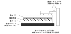
- FIG. 4 is a diagram for explaining a method for measuring peel resistance in another embodiment of the present invention.
- FIG. 4 is a diagram for explaining a method for measuring peel resistance in another embodiment of the present invention.
- (meth)acrylate refers to a compound having one or more (meth)acryloyl groups in one molecule.
- Monofunctional (meth)acrylate refers to a compound having one (meth)acryloyl group in one molecule.
- Polyfunctional (meth)acrylate refers to a compound having two or more (meth)acryloyl groups in one molecule.
- n-functional (meth)acrylate refers to a compound having n (meth)acryloyl groups in one molecule.
- the polymerizable functional group in a polyfunctional (meth)acrylate may have only acryloyl groups, may have only methacryloyl groups, or may have both acryloyl and methacryloyl groups.
- a plate-shaped substrate (1) and an optically transparent plate-shaped substrate (2) are bonded together via a temporary fixing composition (Step A).
- the reason why the substrate (2) is optically transparent is that the temporary fixing composition is irradiated with laser light to harden it to form an adhesive layer, and the adhesive layer is irradiated with laser light to decompose it.
- the substrate to be processed may be either the substrate (1) or the substrate (2), or may be both the substrate (1) and the substrate (2).
- the materials of the substrate (1) and the substrate (2) are not limited, and may be inorganic substrates such as silicon wafers, glass, quartz, sapphire, diamond, indium phosphide, silicon carbide, gallium arsenide, quartz, calcium fluoride, magnesium fluoride, or organic substrates such as plastic.
- inorganic substrates such as silicon wafers, glass, quartz, sapphire, diamond, indium phosphide, silicon carbide, gallium arsenide, quartz, calcium fluoride, magnesium fluoride, or organic substrates such as plastic.
- the specific composition of the temporary fixing composition is not limited as long as it satisfies the conditions that it is curable and decomposable by laser light and generates outgassing upon decomposition, and it may be any composition that is adhesive, such as a (meth)acrylic compound, a urethane compound, an epoxy compound, a silicone compound, other thermoplastic resins, adhesive tape, etc.
- a step of bonding the substrate (1) and the substrate (2) is carried out via a temporary fixing composition preferably containing the following (A), more preferably a temporary fixing composition containing the following (A) to (C).
- A) Polymerizable component B
- Polymerization initiator C
- the polymerizable component (A) contained in the temporary fixing composition of this embodiment is preferably a polymerizable organic compound component, more preferably contains (meth)acrylate.
- the polymerizable component containing (meth)acrylate plays a role in forming a (meth)acrylic polymerization skeleton.
- the temporary fixing composition of this embodiment may also contain a non-polymerizable component, but the amount of the non-polymerizable component is preferably less than 15 parts by mass relative to 100 parts by mass of the total of the non-polymerizable component and the (A) component.
- the term "non-polymerizable component" is defined as anything other than the (B) component, that is, anything not used in the technical field as a polymerization initiator.
- the polymerizable component (A) contained in the temporary fixing composition of this embodiment preferably contains a (meth)acryloyl group, and in this case, the polymerizable component plays a role in forming a (meth)acrylic polymerization skeleton.
- the component (A) may preferably contain a compound having two or more (meth)acryloyl groups.
- the component (A) may be a monofunctional (meth)acrylate, a bifunctional (meth)acrylate, or a trifunctional or higher polyfunctional (meth)acrylate, or a mixture thereof.
- the component (A) may preferably include a combination of a polyfunctional (meth)acrylate and a monofunctional (meth)acrylate (more preferably a combination of a bifunctional (meth)acrylate and a monofunctional (meth)acrylate), a combination of a polyfunctional (meth)acrylate and a polymerizable polymer (more preferably a combination of a bifunctional (meth)acrylate and a polymerizable polymer), or a combination of a polyfunctional (meth)acrylate, a monofunctional (meth)acrylate, and a polymerizable polymer (more preferably a combination of a bifunctional (meth)acrylate, a monofunctional (meth)acrylate, and a polymerizable polymer).
- Component (A) does not have a benzophenone skeleton, a triazole skeleton, a hydroxyphenyltriazine skeleton, or a phenol skeleton (i.e., it does not contain component (C) described below).
- Component (A) preferably does not have a nitrogen atom in the molecule.
- the polyfunctional (meth)acrylate that the (A) component may contain may be an aromatic bifunctional (meth)acrylate, an alicyclic bifunctional (meth)acrylate, or a mixture thereof, from the viewpoint of providing a rigid structure.
- the (A) component may contain an acyclic polyfunctional (meth)acrylate.
- the polyfunctional (meth)acrylate may be a monomer or a polymer, or may be a mixture thereof. That is, the above-mentioned polymerizable polymer may be a polymer of a polyfunctional (meth)acrylate monomer.
- the molecular weight of the polyfunctional (meth)acrylate monomer is preferably 900 or less, more preferably 700 or less, even more preferably 500 or less, and even more preferably 400 or less.
- the molecular weight of the polyfunctional (meth)acrylate monomer is preferably 100 or more, more preferably 200 or more.
- aromatic difunctional (meth)acrylates include 9,9-bis[4-(2-hydroxy C 1 -C 20 alkoxy)phenyl]fluorene di(meth)acrylate, C 1 -C 20 alkoxylated bisphenol A di(meth)acrylate, benzyl di(meth)acrylate, 1,3-bis(2-(meth)acryloyloxy C 1 -C 20 alkyl)benzene, 2,2-bis(4-(meth)acryloxydiethoxyphenyl)propane, or structural isomers thereof.
- di(meth)acrylates having a condensed ring skeleton such as one or more skeletons selected from fluorene, indene, indecene, anthracene, azulene, and triphenylene, may be included.
- alicyclic bifunctional (meth)acrylates include C1 - C20 alkoxylated hydrogenated bisphenol A di(meth)acrylate, 1,3-di(meth)acryloyloxyadamantane, tricyclo C10 - C20 alkane dimethanol di(meth)acrylate, dicyclo C5 - C20 di(meth)acrylate, or structural isomers thereof.
- Examples of acyclic bifunctional or polyfunctional (meth)acrylates include 1,3-butanediol di(meth)acrylate, 1,4-butanediol di(meth)acrylate, 1,6-hexanediol di(meth)acrylate, 1,9-nonanediol di(meth)acrylate, 1,10-decanediol di(meth)acrylate, neopentyl glycol di(meth)acrylate, neopentyl glycol modified trimethylolpropane di(meth)acrylate, stearic acid modified pentaerythritol di(meth)acrylate, tripropylene glycol di(meth)acrylate, and caprolactone modified hydroxypivalic acid neopentyl glycol di(meth)acrylate.
- Component (A) may also contain a polyfunctional (meth)acrylate having three or more functional groups.
- trifunctional (meth)acrylates include ethylene oxide-modified isocyanuric acid tri(meth)acrylate, pentaerythritol tri(meth)acrylate, trimethylolpropane tri(meth)acrylate, and tris[(meth)acryloyloxyethyl]isocyanurate.
- tetrafunctional or higher (meth)acrylates examples include ditrimethylolpropane tetra(meth)acrylate, dimethylolpropane tetra(meth)acrylate, pentaerythritol tetra(meth)acrylate, pentaerythritol ethoxy tetra(meth)acrylate, dipentaerythritol penta(meth)acrylate, and dipentaerythritol hexa(meth)acrylate.
- the monofunctional (meth)acrylate that may be contained in component (A) is preferably a monofunctional (meth)acrylate having a molecular weight of 550 or less, and more preferably a monofunctional alkyl (meth)acrylate having an alkyl group.
- the alkyl group is preferably one or more selected from linear alkyl groups, branched alkyl groups, and alicyclic alkyl groups, and more preferably one or more selected from linear alkyl groups and branched alkyl groups.
- component (A) has a long chain and branched or cyclic alkyl group, for example, a branched alkyl group such as an isostearyl group, an isotetracosanyl group (e.g., 2-decyl-1-tetradecanyl group), or an isotriacontanyl group (e.g., 2-tetradecyl-1-octadecanyl group), having 18 to 40 carbon atoms, more preferably 18 to 32 carbon atoms, or a cycloalkyl group.
- a branched alkyl group such as an isostearyl group, an isotetracosanyl group (e.g., 2-decyl-1-tetradecan
- the monofunctional (meth)acrylate that may be contained in component (A) is preferably one or more selected from the group consisting of stearyl (meth)acrylate, isostearyl (meth)acrylate, behenyl (meth)acrylate, 2-decyl-1-tetradecanyl (meth)acrylate, 2-dodecyl-1-hexadecanyl (meth)acrylate, and 2-tetradecyl-1-octadecanyl (meth)acrylate.
- the monofunctional (meth)acrylate that may be contained in component (A) is preferably the (meth)acrylate of formula 1 below.
- R1 is a hydrogen atom or a methyl group, and preferably a hydrogen atom
- R2 is an alkyl group preferably having 18 to 32 carbon atoms.
- (meth)acrylates having a linear or branched alkyl group such as stearyl(meth)acrylate, isostearyl(meth)acrylate, nonadecyl(meth)acrylate, eicodecyl(meth)acrylate, behenyl(meth)acrylate, 2-decyl-1-tetradecanyl(meth)acrylate, and 2-tetradecyl-1-octadecanyl(meth)acrylate.
- These (meth)acrylates can be used alone or in combination.
- the amount of non-polymerizable components contained in the temporary fixing composition of this embodiment may be 0% by mass or more and less than 10% by mass, or 0% by mass or more and less than 5% by mass. More preferably, the temporary fixing composition of this embodiment may not contain any non-polymerizable components except for component (B).
- the polymerization initiator which is the component (B) contained in the temporary fixing composition of the present embodiment, is a substance that can initiate polymerization of the component (A).
- a photopolymerization initiator is preferable.
- the initiator is a substance capable of initiating polymerization of the (A) component upon irradiation with light.
- a preferred (B) component may be a photoradical polymerization initiator.
- Photoradical polymerization initiators are, for example, those that can be irradiated with ultraviolet or visible light.
- photoradical polymerization initiator examples include bis(2,4,6-trimethylbenzoyl)phenylphosphine oxide, 2,4,6-trimethylbenzoyldiphenylphosphine oxide, bis( ⁇ 5-2,4-cyclopentadiene- 1-yl)-bis(2,6-difluoro-3-(1H-pyrrol-1-yl)-phenyl)titanium, 2-benzyl-2-dimethylamino-1-(4-morpholinophenyl)-butane- 1-one, 2-dimethylamino-2-(4-methylbenzyl)-1-(4-morpholin-4-ylphenyl)-butan-1-one, 1-[4-(phenylthio)phenyl]-1 , 2-octanedione 2-O-benzoyloxime, and 1-[9-ethyl-6-(2-methylbenzoyl)-9H-carbazol-3-yl]ethanone 1-(O-acetyloxime
- the component (B) contained in the temporary fixing composition may contain an acylphosphine oxide compound.
- acylphosphine oxide compounds include bis(2,4,6-trimethylbenzoyl)phenylphosphine oxide and 2,4,6-trimethylbenzoyldiphenylphosphine oxide.
- the polymerization initiator is preferably highly sensitive and has excellent deep curing properties due to its photofading resistance, and also has an absorption wavelength range for generating radicals that extends to a relatively long wavelength range.
- the above-mentioned preferred compounds have an absorption wavelength range up to a wavelength of about 440 nm, which is significantly different from the absorption wavelength range of the UV absorber used in the UV laser peeling described below.
- the degree of UV curing inhibition by the UV absorber is small, and radical polymerization can be initiated with light of a longer wavelength. Therefore, even in the presence of a UV absorber, the effect of initiating radical polymerization and curing efficiently at a relatively high speed can be obtained.
- the polymerization initiator can be selected based on absorbance.
- the polymerization initiator can be selected from one or more compounds that, when dissolved at a concentration of 0.1% by mass in a solvent (e.g., acetonitrile or toluene) that does not have a maximum absorption in the wavelength region of 300 to 500 nm, satisfy one or more of the following conditions: absorbance at a wavelength of 365 nm is 0.5 or more, absorbance at a wavelength of 385 nm is 0.5 or more, and absorbance at a wavelength of 405 nm is 0.5 or more.
- a solvent e.g., acetonitrile or toluene
- Examples of compounds that satisfy such conditions include 1-[9-ethyl-6-(2-methylbenzoyl)-9H-carbazol-3-yl]ethanone 1-(O-acetyloxime), which has an absorbance of 0.5 or more at a wavelength of 365 nm when dissolved in acetonitrile as a solvent at a concentration of 0.1% by mass; 1-[4-(phenylthio)phenyl]-1,2-octanedione 2-O-benzoyloxime, which has an absorbance of 0.5 or more at wavelengths of 365 nm and 385 nm; and bis(2,4,6-trimethylbenzoyl)phenylphosphine oxide and 2,4,6-trimethylbenzoyldiphenylphosphine oxide, which have an absorbance of 0.5 or more at wavelengths of 365 nm, 385 nm, and 405 nm.
- bis( ⁇ 5-2,4-cyclopentadiene-1-yl)-bis(2,6-difluoro-3-(1H-pyrrol-1-yl)-phenyl)titanium which has an absorption wavelength range of 400 to 500 nm, can also be used as a polymerization initiator.
- the (B) polymerization initiator one or more compounds selected from acylphosphine oxide compounds, titanocene compounds, and ⁇ -aminoalkylphenone compounds are preferred in terms of reaction speed, heat resistance after curing, low outgassing, and absorption characteristics in a region different from the wavelength of the UV laser used in the UV laser peeling described below and the absorption wavelength region of the UV absorber used in the UV laser peeling.
- oxime ester compounds can also be selected as polymerization initiators for resin compositions for temporary fixing applications for preventing damage from bonding to the support member of the substrate to be processed until the heating step, which is not a layer for UV laser peeling, among the temporary fixing compositions having the structure described below.
- Acylphosphine oxide compounds include bis(2,4,6-trimethylbenzoyl)phenylphosphine oxide and 2,4,6-trimethylbenzoyldiphenylphosphine oxide. Of these, bis(2,4,6-trimethylbenzoyl)phenylphosphine oxide is particularly preferred.
- Titanocene compounds include bis( ⁇ 5-2,4-cyclopentadiene-1-yl)-bis(2,6-difluoro-3-(1H-pyrrol-1-yl)-phenyl)titanium.
- ⁇ -aminoalkylphenone compounds examples include 2-benzyl-2-dimethylamino-1-(4-morpholinophenyl)-butan-1-one and 2-dimethylamino-2-(4-methylbenzyl)-1-(4-morpholin-4-ylphenyl)-butan-1-one.
- Oxime ester compounds include 1-[4-(phenylthio)phenyl]-1,2-octanedione 2-O-benzoyloxime, 1-[9-ethyl-6-(2-methylbenzoyl)-9H-carbazol-3-yl]ethanone 1-(O-acetyloxime), etc. Among these, 1-[9-ethyl-6-(2-methylbenzoyl)-9H-carbazol-3-yl]ethanone 1-(O-acetyloxime) is preferred.
- component (B) in the temporary fixing composition is one or more selected from bis(2,4,6-trimethylbenzoyl)phenylphosphine oxide, 2,4,6-trimethylbenzoyldiphenylphosphine oxide, and 1-[9-ethyl-6-(2-methylbenzoyl)-9H-carbazol-3-yl]ethanone 1-(O-acetyloxime).
- the amount of (B) polymerization initiator used is preferably 0.01 to 10 parts by mass, more preferably 0.01 to 5 parts by mass, and most preferably 0.01 to 3 parts by mass, relative to 100 parts by mass of the total of (A) components, in terms of reaction speed, heat resistance after curing, and low outgassing. Typically, it can be 0.1 to 2 parts by mass, and can be 0.1 to 1 part by mass.
- the (B) component is 0.01 part by mass or more, sufficient curing properties are obtained, and when it is 10 parts by mass or less, the effect of low outgassing properties and heat resistance being less likely to be impaired is obtained.
- UV absorbing agent which is the component (C) contained in the temporary fixing composition of the present embodiment is decomposed and vaporized by being irradiated with ultraviolet light or a visible light laser, and the decomposition and vaporization
- the compound is generated at the interface between the support member and the adhesive layer obtained by curing the temporary fixing composition, and causes a loss of adhesive strength between the adhesive layer and the support member that was maintained until just before the peeling process.
- the component (C) is preferably a compound having one or more selected from the group consisting of a benzophenone skeleton, a triazole skeleton, a hydroxyphenyltriazine skeleton, and a phenol skeleton (preferably a hindered phenol skeleton), and more preferably These compounds have a hydroxyphenyltriazine skeleton.
- the reason they have these skeletons is to obtain the degree of overlap with the UV laser wavelength in the UV absorption wavelength region, UV absorption characteristics at the same wavelength, low outgassing, and heat resistance.
- Examples of ultraviolet absorbents having a hydroxyphenyltriazine skeleton include 2-(2-hydroxy-4-[1-octyloxycarbonylethoxy]phenyl)-4,6-bis(4-phenylphenyl)-1,3, 5-Triazine is preferred.
- the ultraviolet absorber which is the component (C) contained in the temporary fixing composition of the present embodiment, is preferably an ultraviolet absorber having a polymerizable functional group.
- the polymerizable functional group of the component (C) is preferably a (meth) An acryloyl group is preferred.
- Examples of the (C) component which is an ultraviolet absorber having a polymerizable functional group, include 2-[2-hydroxy-5-[2-((meth)acryloyloxy)ethyl]phenyl]-2H-benzotriazole, 2-[1-(2-hydroxy-3,5-di-tert-pentylphenyl)ethyl]-4,6-di-tert-pentylphenyl (meth)acrylate, 2-(2-(2-(meth)acryloyloxy,5-methyl)phenyl-2H-benzotriazole, 1,1-bis-[2-(meth)acryloyloxy,3-(2H-benzotriazol-2-yl),5-tert-octyl]methane, and 2,2'-dihydroxy-4,4'-di(meth)acryloyloxybenzophenone, which are particularly preferred in terms of compatibility with the resin component, UV absorption properties, low outgassing, and heat resistance.
- the amount of component (C) is preferably 0.01 to 15 parts by mass, more preferably 0.1 to 12 parts by mass, even more preferably 0.5 to 10 parts by mass, and even more preferably 0.5 to 7 parts by mass, per 100 parts by mass of component (A). If it is 0.01 part by mass or more, a sufficient UV laser peeling speed can be obtained, and if it is 15 parts by mass or less, the effect of low outgassing properties and heat resistance not being easily impaired can be obtained.
- the method for bonding the substrate (1) and the substrate (2) is not particularly limited, but is typically performed by applying a temporary fixing adhesive to the substrate (2) and then bonding the substrate (1) to the surface to which the temporary fixing adhesive has been applied.
- the temporary fixing adhesive can be applied by known application methods such as spin coating, screen printing, and various coaters.
- the viscosity of the temporary fixing composition of this embodiment is preferably 500 mPa ⁇ s or more, and more preferably 1000 mPa ⁇ s or more, in terms of application and workability at 23°C (atmospheric pressure).
- the viscosity of the temporary fixing composition of this embodiment is preferably 15000 mPa ⁇ s or less, more preferably 10000 mPa ⁇ s or less, and even more preferably 5000 mPa ⁇ s or less, in terms of application and workability at 23°C (atmospheric pressure).
- a viscosity of 500 mPa ⁇ s or more provides excellent application properties, particularly application properties by spin coating.
- a viscosity of 15000 mPa ⁇ s or less provides excellent workability.
- the viscosity can be measured by a known viscometer.
- Spin coating is a method in which, for example, a liquid composition is dropped onto the substrate (2) and the substrate (2) is rotated at a predetermined rotation speed, thereby applying the composition to the surface of the substrate (2).
- Spin coating can efficiently produce high-quality coating films.
- step B the temporary fixing composition is cured to form an adhesive layer, and the substrate (1) and the substrate (2) are bonded together.
- the irradiation conditions are not particularly limited, but it is preferable to irradiate with visible light or ultraviolet light (wavelength or central wavelength 365 to 405 nm) so that the energy amount is 1 to 20,000 mJ/cm 2. If the energy amount is 1 mJ/cm 2 or more, sufficient adhesive strength is obtained, and if it is 20,000 mJ/cm 2 or less, productivity is excellent, decomposition products from the polymerization initiator are unlikely to be generated, and outgassing is suppressed. In terms of productivity, adhesive strength, low outgassing, and easy peeling, it is preferable that the energy amount is 1,000 to 10,000 mJ/cm 2 .
- the substrate (2) as the support member is not particularly limited as long as it is optically transparent.
- transparent substrates include inorganic substrates such as glass, quartz, sapphire, diamond, indium phosphide, silicon carbide, gallium arsenide, quartz, calcium fluoride, and magnesium fluoride, and organic substrates such as plastic.
- inorganic substrates are preferred because of their versatility and the large effects they can provide.
- one or more selected from glass and quartz are preferred. Glass is particularly preferred.
- Step C After the substrate (1) and the substrate (2) are bonded together, the substrate (1) or the substrate (2) is processed.
- a process is carried out in which the substrate (1) is processed to form a thin wafer.
- the type of processing is not particularly limited, but typically includes thinning by grinding and polishing, molding, and heat treatment.
- step D a laser beam is irradiated from the substrate (2) side to decompose the adhesive layer to generate outgassing, and the substrate (1) and substrate (2) are peeled off by the outgassing.
- the adhesive layer is formed by curing the temporary fixing composition due to the adhesion between the substrate (1) and substrate (2).
- the substrate (1) or substrate (2) can be peeled off by irradiating the substrate (1) with a laser beam from the substrate (2) side so as to scan the entire surface.
- a step of irradiating the substrate with light having a wavelength of 385 nm or less, more preferably 300 to 385 nm, to decompose the adhesive layer is carried out.
- the adhesive layer can be decomposed by irradiating the substrate (1) with a UV laser having a wavelength of 300 to 385 nm so as to scan the entire surface.
- the substrate (1) can be peeled off from the substrate (2).
- the linear region has a shape that surrounds a portion or all of the adhesive layer, and the area of the adhesive layer surrounded by the linear region is 90.2% or more of the total area of the adhesive layer.
- the substrates may re-adhere to each other. This is thought to be caused by outgassing generated by the decomposition of the adhesive layer, which escapes from between the substrates over time, causing the substrates to come into contact with each other. Since outgassing acts as a cushion to prevent the substrates from coming into contact with each other, it is thought that re-adhesion can be prevented by suppressing its dispersion.
- FIG. 1 shows a method of masking arrangement in one embodiment of the present invention.
- This figure is a top view seen from the substrate (2) side.
- the adhesive layer is formed over the entire surface of the substrate (2), so the area of the substrate (2) is the same as the area of the adhesive layer.
- a portion of the surface of the substrate (2) is linearly masked to form a linear region where the adhesive layer is not irradiated with laser light. Since the linear region is not irradiated with laser light, the adhesive layer does not decompose, and therefore outgassing generated by decomposition of the adhesive layer inside the linear region does not easily disperse. This makes it possible to prevent contact between the substrate (1) and the substrate (2) even over a long period of time, and thus to prevent re-adhesion.
- the area of the adhesive layer surrounded by the linear region (hereinafter also referred to as "outgassing retention area") must be 90.2% or more of the total area of the adhesive layer.
- the outgassing retention area is preferably 91% or more of the total area of the adhesive layer, more preferably 92% or more, even more preferably 93% or more, even more preferably 94% or more, and even more preferably 95% or more.
- the outgassing retention area is typically 96% or less of the total area of the adhesive layer. In one preferred embodiment of the present invention, the area is 95.50 to 97.00%.
- the peel resistance described below can be reduced to a particularly desirable range.
- the adhesive layer does not cover the entire surface of the substrate (2) but is formed only on the portion inside the linear region, the outgassing retention area is 100% of the total area of the adhesive layer.
- the portion of the adhesive layer that is surrounded by the linear region is also referred to as the "surrounded portion.”
- the area of the adhesive layer surrounded by a linear region is the area surrounded by the inner contour of the linear region, i.e., the area of the linear region itself is not taken into consideration.
- the ratio of the mask length to the outgas retention length of the length from the peeling start point to the peeling end point is 0.15% or more in step D. More specifically, this ratio is a value (%) calculated by the formula L2/L1 ⁇ 100, where L1 is the outgas retention length (i.e., the length of the surrounded part on the straight line S) connecting the peeling start point and the peeling end point, and L2 is the mask length (i.e., the length of the mask on the straight line S).
- L1 is the outgas retention length (i.e., the length of the surrounded part on the straight line S) connecting the peeling start point and the peeling end point
- L2 is the mask length (i.e., the length of the mask on the straight line S).
- 2A and 2B show a method for measuring the outgas retention length and the mask length in one embodiment of the present invention. As shown in FIG.
- a suction arm with a suction cup is attached to the substrate (2), and the substrate (2) is peeled off by vertically pulling the suction arm upward.
- the point where the substrate (2) starts to peel off and the point where the peeling ends are set as the peeling start point and the peeling end point, respectively, and a straight line S is drawn connecting the two.
- the length passing through the surrounded part having the outgas retention area is set as the outgas retention length
- the length passing through the linear region is set as the mask length.
- the mask length is the sum of the length at a point close to the peeling start point and the length at a point close to the peeling end point.
- the above-mentioned peel start point and peel end point are preferably located on a straight line S passing near the center of the substrate 2.
- the straight line S is usually set at a position corresponding to the longest diagonal of the maximum diameter M of the substrate 2.
- the ratio of the mask length to the outgas retention length is preferably 0.20% or more, more preferably 0.25% or more, and even more preferably 0.30% or more.
- the upper limit of the ratio of the mask length to the outgas retention length a smaller mask length makes it easier to ensure an outgas retention area, so that the upper limit is preferably 1.00% or less, more preferably 0.90% or less, even more preferably 0.80% or less, and even more preferably 0.70% or less.
- the ratio is 0.30 to 0.50%. When the ratio is within this range, the peel resistance, which will be described later, can be reduced to a particularly desirable range.
- the masking line width be 0.2 mm or more over 95% or more of the entire circumference of the linear region.
- the masking line width is the distance between the inner contour line and the outer contour line of the linear region measured at each point in a direction perpendicular to the center line of the linear region, as shown in Figure 3. If the masking line width measured over 95% or more of the length of the center line is 0.2 mm or more, the outgassing can be more reliably retained, and the effect of suppressing re-adhesion can be further improved.
- the masking line width is more preferably 0.3 mm or more, more preferably 0.4 mm or more, and even more preferably 0.5 mm or more.
- the upper limit of the masking line width is preferably 1.2 mm or less, since a smaller masking line width makes it easier to ensure an outgassing retention area, and can be, for example, 1.0 mm or less, 0.8 mm or less, or 0.6 mm or less.
- the aforementioned mask length may be exactly twice the masking line width, but this relationship is not necessarily required.
- the linear region may have a partially open shape. If the linear region is partially open, the undecomposed adhesive layer will have an open shape rather than a closed shape, making it easier to insert the tip of a peeling device when peeling the substrates apart, and easier to physically peel them apart. On the other hand, if the opening in the linear region is too large, the outgassing retention effect may be compromised, so it is preferable that the linear region does not open. In other words, it is preferable that the linear region forms a closed shape.
- the linear region does not necessarily have to be entirely curved, and may have an acute angle, a right angle, or an obtuse angle in part. More typically, as shown in Fig. 5, for example, the linear region may have a pointed portion (protrusion) as long as the outgassing retention area satisfies the requirements of the present invention.
- the protrusion may function as a mark for alignment during masking or peeling.
- the linear region may be provided so that only one surrounded portion is formed as shown in FIG. 1, or may be provided so that multiple surrounded portions are formed as shown in FIG. 4.
- the peel resistance is preferably 40 N or less. In a further preferred embodiment of the present invention, the peel resistance is 30 N or less, and even more preferably 20 N or less.
- peel resistance is measured as follows. As shown in Figure 6B, the substrate (1) is placed face down on a suction table such as a porous chuck type and fixed in place, and a suction arm with three suction cups with a diameter of 10 mm is attached from above to the substrate (2) of the test piece (see Figure 6A). The substrate (2) is peeled off by vertically pulling the suction arm upward at 0.5 mm/s, and the load on the suction arm when the substrate (2) is lifted is measured and this is taken as the measured value of peel resistance.
- a suction table such as a porous chuck type and fixed in place
- a suction arm with three suction cups with a diameter of 10 mm is attached from above to the substrate (2) of the test piece (see Figure 6A).
- the substrate (2) is peeled off by vertically pulling the suction arm upward at 0.5 mm/s, and the load on the suction arm when the substrate (2) is lifted is measured and this is taken as the measured value of peel resistance.
- thermofixing composition The following was used as component (A).
- A-DOD-N 1,10-decanediol diacrylate ("A-DOD-N" manufactured by Shin-Nakamura Chemical Co., Ltd., molecular weight 282)
- Tinuvin 479 Hydroxyphenyltriazine (HPT) type ultraviolet absorber (2-(2-hydroxy-4-[1-octyloxycarbonylethoxy]phenyl)-4,6-bis(4-phenylphenyl)-1,3,5-triazine, "Tinuvin 479" manufactured by BSAF)
- a UV laser with a wavelength of 355 nm was irradiated onto a circular area with a diameter of 110 mm fixed at the center of the obtained 4-inch test piece so as to scan the entire surface of the test piece from the glass support member side.
- the UV laser used was a UV laser QLA-355 manufactured by Quark Technology, with an output of 8.5 W, a frequency of 40 kHz, a scan pitch of 200 ⁇ m, and a beam diameter of 200 ⁇ m.
- the substrate (1) was placed face down on a suction table such as a porous chuck type and fixed in place, and a suction arm equipped with three suction cups (made of fluororubber) with a diameter of 10 mm was attached from above to the substrate (2) of the test piece (the bonded sample was adsorbed at a position 1 mm from the end), and the substrate (2) was peeled off by vertically pulling the suction arm upward at 0.5 mm/s. The load on the suction arm when the substrate (2) was lifted was measured, and this was taken as the measured peel resistance.
- a suction table such as a porous chuck type and fixed in place
- a suction arm equipped with three suction cups made of fluororubber
- Example 10 in which protrusions were provided on the linear regions of the masking also had low peel resistance.
- Example 3 is the same as Example 2 except that the peel resistance was measured 24 hours after the UV laser irradiation was completed, and it can be seen that the peel resistance was maintained sufficiently low.
- Comparative Example 1 because masking was not performed, re-adhesion occurred and peel resistance increased (more than 20 N but less than 30 N).
- Comparative Example 2 because the ratio of the mask length to the outgas retention length was less than 0.15%, the outgas could not be retained, the mask broke, and peel resistance increased.
- Comparative Example 3 because the outgas retention area was less than 90.2%, the amount of outgas was insufficient to peel off the masked portion, and peel resistance increased.
Landscapes
- Chemical & Material Sciences (AREA)
- Organic Chemistry (AREA)
- Health & Medical Sciences (AREA)
- Chemical Kinetics & Catalysis (AREA)
- Medicinal Chemistry (AREA)
- Polymers & Plastics (AREA)
- Adhesives Or Adhesive Processes (AREA)
- Laser Beam Processing (AREA)
Priority Applications (4)
| Application Number | Priority Date | Filing Date | Title |
|---|---|---|---|
| JP2025506805A JPWO2024190671A1 (https=) | 2023-03-10 | 2024-03-08 | |
| CN202480016975.5A CN120826777A (zh) | 2023-03-10 | 2024-03-08 | 板状基材的加工方法 |
| KR1020257029490A KR20250144436A (ko) | 2023-03-10 | 2024-03-08 | 판형 기재의 가공 방법 |
| EP24770777.1A EP4664509A1 (en) | 2023-03-10 | 2024-03-08 | Method for processing plate-shaped base material |
Applications Claiming Priority (2)
| Application Number | Priority Date | Filing Date | Title |
|---|---|---|---|
| JP2023-038006 | 2023-03-10 | ||
| JP2023038006 | 2023-03-10 |
Publications (1)
| Publication Number | Publication Date |
|---|---|
| WO2024190671A1 true WO2024190671A1 (ja) | 2024-09-19 |
Family
ID=92755619
Family Applications (1)
| Application Number | Title | Priority Date | Filing Date |
|---|---|---|---|
| PCT/JP2024/009061 Ceased WO2024190671A1 (ja) | 2023-03-10 | 2024-03-08 | 板状基材の加工方法 |
Country Status (6)
| Country | Link |
|---|---|
| EP (1) | EP4664509A1 (https=) |
| JP (1) | JPWO2024190671A1 (https=) |
| KR (1) | KR20250144436A (https=) |
| CN (1) | CN120826777A (https=) |
| TW (1) | TWI889231B (https=) |
| WO (1) | WO2024190671A1 (https=) |
Citations (7)
| Publication number | Priority date | Publication date | Assignee | Title |
|---|---|---|---|---|
| JP2005159155A (ja) | 2003-11-27 | 2005-06-16 | Three M Innovative Properties Co | 半導体チップの製造方法 |
| JP2007273500A (ja) * | 2006-03-30 | 2007-10-18 | Tokyo Ohka Kogyo Co Ltd | サポートプレートの剥離方法 |
| JP2014053623A (ja) * | 2012-08-07 | 2014-03-20 | Sekisui Chem Co Ltd | ウエハの処理方法 |
| JP2014129431A (ja) * | 2012-12-27 | 2014-07-10 | Fujifilm Corp | 半導体装置製造用仮接着剤、並びに、それを用いた接着性支持体、及び、半導体装置の製造方法 |
| JP2016525801A (ja) * | 2013-08-01 | 2016-08-25 | インターナショナル・ビジネス・マシーンズ・コーポレーションInternational Business Machines Corporation | 中波長赤外線アブレーションを用いるウェハ剥離 |
| WO2021192854A1 (ja) * | 2020-03-24 | 2021-09-30 | 東京エレクトロン株式会社 | 基板処理方法及び基板処理装置 |
| JP2023038006A (ja) | 2021-09-06 | 2023-03-16 | 国立研究開発法人農業・食品産業技術総合研究機構 | 花の老化が遅延されたユリ植物及びその製造方法 |
Family Cites Families (5)
| Publication number | Priority date | Publication date | Assignee | Title |
|---|---|---|---|---|
| US20160218077A1 (en) * | 2013-09-30 | 2016-07-28 | Lintec Corporation | Composite Sheet for Resin Film Formation |
| JP7470047B2 (ja) | 2018-11-14 | 2024-04-17 | デンカ株式会社 | 組成物 |
| CN113825635A (zh) * | 2019-03-28 | 2021-12-21 | 琳得科株式会社 | 粘合片、粘合片的制造方法及半导体装置的制造方法 |
| US12480025B2 (en) * | 2020-05-21 | 2025-11-25 | Denka Company Limited | Composition |
| CN117242146A (zh) * | 2021-04-26 | 2023-12-15 | 电化株式会社 | 组合物 |
-
2024
- 2024-03-08 JP JP2025506805A patent/JPWO2024190671A1/ja active Pending
- 2024-03-08 TW TW113108599A patent/TWI889231B/zh active
- 2024-03-08 KR KR1020257029490A patent/KR20250144436A/ko active Pending
- 2024-03-08 CN CN202480016975.5A patent/CN120826777A/zh active Pending
- 2024-03-08 WO PCT/JP2024/009061 patent/WO2024190671A1/ja not_active Ceased
- 2024-03-08 EP EP24770777.1A patent/EP4664509A1/en active Pending
Patent Citations (7)
| Publication number | Priority date | Publication date | Assignee | Title |
|---|---|---|---|---|
| JP2005159155A (ja) | 2003-11-27 | 2005-06-16 | Three M Innovative Properties Co | 半導体チップの製造方法 |
| JP2007273500A (ja) * | 2006-03-30 | 2007-10-18 | Tokyo Ohka Kogyo Co Ltd | サポートプレートの剥離方法 |
| JP2014053623A (ja) * | 2012-08-07 | 2014-03-20 | Sekisui Chem Co Ltd | ウエハの処理方法 |
| JP2014129431A (ja) * | 2012-12-27 | 2014-07-10 | Fujifilm Corp | 半導体装置製造用仮接着剤、並びに、それを用いた接着性支持体、及び、半導体装置の製造方法 |
| JP2016525801A (ja) * | 2013-08-01 | 2016-08-25 | インターナショナル・ビジネス・マシーンズ・コーポレーションInternational Business Machines Corporation | 中波長赤外線アブレーションを用いるウェハ剥離 |
| WO2021192854A1 (ja) * | 2020-03-24 | 2021-09-30 | 東京エレクトロン株式会社 | 基板処理方法及び基板処理装置 |
| JP2023038006A (ja) | 2021-09-06 | 2023-03-16 | 国立研究開発法人農業・食品産業技術総合研究機構 | 花の老化が遅延されたユリ植物及びその製造方法 |
Non-Patent Citations (1)
| Title |
|---|
| See also references of EP4664509A1 |
Also Published As
| Publication number | Publication date |
|---|---|
| TWI889231B (zh) | 2025-07-01 |
| EP4664509A1 (en) | 2025-12-17 |
| KR20250144436A (ko) | 2025-10-10 |
| CN120826777A (zh) | 2025-10-21 |
| TW202441586A (zh) | 2024-10-16 |
| JPWO2024190671A1 (https=) | 2024-09-19 |
Similar Documents
| Publication | Publication Date | Title |
|---|---|---|
| JP7629143B2 (ja) | 仮固定用組成物、仮固定用接着剤、及び薄型ウエハの製造方法 | |
| JP7717769B2 (ja) | 組成物 | |
| WO2018051961A1 (ja) | パターン形成方法および半導体素子の製造方法 | |
| KR20140047003A (ko) | 웨이퍼 가공체, 웨이퍼 가공용 부재, 웨이퍼 가공용 가접착재, 및 박형 웨이퍼의 제조방법 | |
| JP2024151339A (ja) | 仮固定用組成物 | |
| JP6695988B2 (ja) | インプリント用プライマ層形成用組成物、インプリント用プライマ層および積層体 | |
| WO2024190671A1 (ja) | 板状基材の加工方法 | |
| JP7628657B2 (ja) | 仮固定用組成物、仮固定用接着剤、及び薄型ウエハの製造方法 | |
| WO2024162057A1 (ja) | 組成物 | |
| JP7587731B1 (ja) | 複数の薄型ウエハの製造方法 | |
| WO2023181609A1 (ja) | 仮固定用組成物 | |
| WO2025192625A1 (ja) | 組成物、仮固定用組成物、及びこれを用いたウエハの製造方法 | |
| TW202440834A (zh) | 抑制氣泡殘留之暫時固定用組合物 |
Legal Events
| Date | Code | Title | Description |
|---|---|---|---|
| 121 | Ep: the epo has been informed by wipo that ep was designated in this application |
Ref document number: 24770777 Country of ref document: EP Kind code of ref document: A1 |
|
| ENP | Entry into the national phase |
Ref document number: 1020257029490 Country of ref document: KR Free format text: ST27 STATUS EVENT CODE: A-0-1-A10-A15-NAP-PA0105 (AS PROVIDED BY THE NATIONAL OFFICE) |
|
| WWE | Wipo information: entry into national phase |
Ref document number: 202480016975.5 Country of ref document: CN |
|
| ENP | Entry into the national phase |
Ref document number: 2025506805 Country of ref document: JP Kind code of ref document: A |
|
| WWE | Wipo information: entry into national phase |
Ref document number: 2025506805 Country of ref document: JP |
|
| WWP | Wipo information: published in national office |
Ref document number: 1020257029490 Country of ref document: KR |
|
| NENP | Non-entry into the national phase |
Ref country code: DE |
|
| WWP | Wipo information: published in national office |
Ref document number: 202480016975.5 Country of ref document: CN |
|
| WWP | Wipo information: published in national office |
Ref document number: 2024770777 Country of ref document: EP |