WO2024157663A1 - 接合体の製造方法および接合方法 - Google Patents
接合体の製造方法および接合方法 Download PDFInfo
- Publication number
- WO2024157663A1 WO2024157663A1 PCT/JP2023/045518 JP2023045518W WO2024157663A1 WO 2024157663 A1 WO2024157663 A1 WO 2024157663A1 JP 2023045518 W JP2023045518 W JP 2023045518W WO 2024157663 A1 WO2024157663 A1 WO 2024157663A1
- Authority
- WO
- WIPO (PCT)
- Prior art keywords
- substrate
- bonding
- sio
- layer
- bonded
- Prior art date
- Legal status (The legal status is an assumption and is not a legal conclusion. Google has not performed a legal analysis and makes no representation as to the accuracy of the status listed.)
- Ceased
Links
Images


Classifications
-
- H—ELECTRICITY
- H10—SEMICONDUCTOR DEVICES; ELECTRIC SOLID-STATE DEVICES NOT OTHERWISE PROVIDED FOR
- H10N—ELECTRIC SOLID-STATE DEVICES NOT OTHERWISE PROVIDED FOR
- H10N30/00—Piezoelectric or electrostrictive devices
- H10N30/01—Manufacture or treatment
- H10N30/07—Forming of piezoelectric or electrostrictive parts or bodies on an electrical element or another base
- H10N30/072—Forming of piezoelectric or electrostrictive parts or bodies on an electrical element or another base by laminating or bonding of piezoelectric or electrostrictive bodies
-
- H—ELECTRICITY
- H10—SEMICONDUCTOR DEVICES; ELECTRIC SOLID-STATE DEVICES NOT OTHERWISE PROVIDED FOR
- H10N—ELECTRIC SOLID-STATE DEVICES NOT OTHERWISE PROVIDED FOR
- H10N30/00—Piezoelectric or electrostrictive devices
- H10N30/01—Manufacture or treatment
- H10N30/03—Assembling devices that include piezoelectric or electrostrictive parts
-
- H—ELECTRICITY
- H10—SEMICONDUCTOR DEVICES; ELECTRIC SOLID-STATE DEVICES NOT OTHERWISE PROVIDED FOR
- H10N—ELECTRIC SOLID-STATE DEVICES NOT OTHERWISE PROVIDED FOR
- H10N30/00—Piezoelectric or electrostrictive devices
- H10N30/01—Manufacture or treatment
- H10N30/07—Forming of piezoelectric or electrostrictive parts or bodies on an electrical element or another base
- H10N30/074—Forming of piezoelectric or electrostrictive parts or bodies on an electrical element or another base by depositing piezoelectric or electrostrictive layers, e.g. aerosol or screen printing
-
- H—ELECTRICITY
- H10—SEMICONDUCTOR DEVICES; ELECTRIC SOLID-STATE DEVICES NOT OTHERWISE PROVIDED FOR
- H10N—ELECTRIC SOLID-STATE DEVICES NOT OTHERWISE PROVIDED FOR
- H10N30/00—Piezoelectric or electrostrictive devices
- H10N30/01—Manufacture or treatment
- H10N30/08—Shaping or machining of piezoelectric or electrostrictive bodies
- H10N30/085—Shaping or machining of piezoelectric or electrostrictive bodies by machining
- H10N30/086—Shaping or machining of piezoelectric or electrostrictive bodies by machining by polishing or grinding
-
- H—ELECTRICITY
- H10—SEMICONDUCTOR DEVICES; ELECTRIC SOLID-STATE DEVICES NOT OTHERWISE PROVIDED FOR
- H10W—GENERIC PACKAGES, INTERCONNECTIONS, CONNECTORS OR OTHER CONSTRUCTIONAL DETAILS OF DEVICES COVERED BY CLASS H10
- H10W72/00—Interconnections or connectors in packages
- H10W72/071—Connecting or disconnecting
- H10W72/073—Connecting or disconnecting of die-attach connectors
- H10W72/07331—Connecting techniques
Definitions
- the present invention relates to a method for manufacturing a bonded body and a bonding method.
- SOI substrates consisting of high-resistance Si/ SiO2 thin film/Si thin film are widely used.
- Plasma activation is used to realize SOI substrates. This method allows the substrates to be bonded at a relatively low temperature (400°C).
- a composite substrate consisting of Si/ SiO2 thin film/piezoelectric thin film similar to SOI substrates has been proposed to improve the characteristics of piezoelectric devices.
- Patent Document 1 discloses a method for manufacturing a composite wafer. This method for manufacturing a composite wafer includes at least the steps of: injecting hydrogen atomic ions or hydrogen molecular ions from the surface to form an ion-implanted layer inside the oxide single crystal wafer; performing a surface activation treatment on at least one of the ion-implanted surface of the oxide single crystal wafer and the surface of the support wafer; bonding the ion-implanted surface of the oxide single crystal wafer and the surface of the support wafer to obtain a bonded body; heat-treating the bonded body at a temperature of 90°C or higher at which cracks do not occur; and irradiating the heat-treated bonded body with visible light to obtain an oxide single crystal thin film that is peeled off along the ion-implanted layer and transferred onto the support wafer.
- An object of the present invention is to provide a manufacturing method and a bonding method for a bonded body that can achieve both reduced void generation and high bonding strength.
- the present invention provides a method for producing a bonded body, the method including, in this order, an activation step of activating, by plasma, the respective surfaces of a first substrate and a second substrate, each having a surface mainly composed of SiO2, a bonding step of bonding the surfaces of the first substrate and the second substrate together at a vacuum degree of 1 mbar or more and 400 mbar or less, and a heating step of heating the bonded first substrate and second substrate.
- the present invention also provides a bonding method including, in this order, an activation step of activating the surfaces of the first SiO 2 layer and the second SiO 2 layer by plasma, a bonding step of bonding the surfaces of the first SiO 2 layer and the second SiO 2 layer together at a vacuum degree of 1 mbar or more and 400 mbar or less, and a heating step of heating the bonded first SiO 2 layer and second SiO 2 layer to remove water generated at the bonding surfaces.
- the present invention provides a method for manufacturing and bonding a bonded body that can reduce the occurrence of voids while maintaining bonding strength.
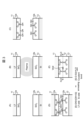
- FIG. 2 is a diagram showing a bonded body according to the present embodiment.
- 1 is a flowchart illustrating a method for manufacturing a bonded body 1.
- 3A to 3E are diagrams showing the states corresponding to the respective steps shown in FIG. 2.
- FIG. 1 is a diagram showing the results of Example 1.
- 4A to 4C are diagrams showing the results of Comparative Examples 1 to 3.
- FIG. 13 is a diagram showing the relationship between the degree of vacuum and the number of voids.
- FIG. 1 is a diagram showing a bonded body 1 according to the present embodiment.
- the illustrated bonded body 1 has a structure in which a piezoelectric layer 11a, a dielectric layer 12, and a support substrate 13 are laminated in this order from the top in the figure.
- the piezoelectric layer 11a is a layer made of a piezoelectric material.
- the piezoelectric material is selected depending on the application of the bonded body 1.
- the piezoelectric material is, for example, LiNbO 3 (LN) or LiTaO 3 (LT), but is not limited thereto.
- Silicon (Si), gallium arsenide (GaAs), silicon carbide (SiC), gallium nitride (GaN), zinc oxide (ZnO), solid solution ceramics (PZT), or the like may be appropriately selected.
- the dielectric layer 12 is a layer disposed under the piezoelectric layer 11a.
- the dielectric layer 12 is mainly composed of SiO 2. That is, it can also be said that the dielectric layer 12 is a SiO 2 film or a SiO 2 layer.
- the support substrate 13 serves as a support for the entire bonded body 1.
- the support substrate 13 is bonded to the piezoelectric layer 11a via the dielectric layer 12. Any appropriate substrate may be used as the support substrate 13.
- the support substrate 13 may be made of a single crystal or a polycrystalline material. It may also be made of a metal.
- the material constituting the support substrate 13 is preferably selected from the group consisting of silicon, sialon, sapphire, cordierite, mullite, glass, quartz, crystal, alumina, SUS, iron-nickel alloy (42 alloy), and brass.
- the thickness of the support substrate 13 is, for example, 0.2 to 1 mm, but any other appropriate thickness may be adopted.
- the silicon may be single crystal silicon, polycrystalline silicon, or high resistance silicon.
- the support substrate 13 may be SOI (Silicon on Insulator).
- the sialon is a ceramic obtained by sintering a mixture of silicon nitride and alumina, and has a composition represented by, for example, Si6 - wAlwOwN8 -w .
- the sialon has a composition in which alumina is mixed into silicon nitride , and w in the formula represents the mixing ratio of alumina. w is preferably 0.5 or more and 4.0 or less.
- the sapphire is a single crystal having a composition of Al 2 O 3
- the alumina is a polycrystalline body having a composition of Al 2 O 3.
- the alumina is preferably translucent alumina.
- the cordierite is a ceramic having a composition of 2MgO.2Al 2 O 3.5SiO 2
- the mullite is a ceramic having a composition in the range of 3Al 2 O 3.2SiO 2 to 2Al 2 O 3.SiO 2 .
- the structure of the bonded body 1 shown in the figure can be used as the structure of various devices, such as high-frequency devices, power semiconductors, semiconductor lasers, surface acoustic wave filters (SAW (Surface Acoustic Wave) filters), thin-film piezoelectric MEMS (Micro Electro Mechanical Systems), etc.
- SAW Surface Acoustic Wave
- MEMS Micro Electro Mechanical Systems
- Fig. 2 is a flow chart illustrating a method for manufacturing the bonded body 1.
- Figs. 3(A) to 3(E) are diagrams showing the states corresponding to the respective steps shown in Fig. 2.
- a piezoelectric material substrate 11 is prepared, and a dielectric layer 12a is formed on the surface of the piezoelectric material substrate 11 (step 101).
- a support substrate 13 is prepared, and a dielectric layer 12b is formed on the surface of the support substrate 13 (step 102).
- dielectric layers 12a and 12b are formed on the surfaces of the piezoelectric material substrate 11 and the support substrate 13 (dielectric layer forming step: FIG. 3(A)). Note that the order of steps 101 and 102 may be reversed.
- the "surface” refers to the main surface of the piezoelectric material substrate 11 and the support substrate 13, not the side surface.
- the piezoelectric material substrate 11 on which the dielectric layer 12a is formed is an example of a first substrate having a surface (surface layer) mainly composed of SiO 2.
- the support substrate 13 on which the dielectric layer 12b is formed is an example of a second substrate having a surface (surface layer) mainly composed of SiO 2.
- the first substrate is the piezoelectric material substrate 11 on which a SiO 2 film is formed
- the second substrate is the support substrate 13 on which a SiO 2 film is formed.
- the dielectric layers 12a and 12b are mainly composed of SiO 2.
- the dielectric layers 12a and 12b are integrated by bonding in a later process to form the dielectric layer 12 mainly composed of SiO 2.
- the dielectric layers 12a and 12b can be formed by reactive sputtering using a reactive sputtering device. Specifically, the piezoelectric material substrate 11 and the support substrate 13 are placed in the reactive sputtering device. A target made of silicon (Si) is also placed in the reactive sputtering device. Furthermore, argon (Ar) gas and oxygen radicals are introduced into the reactive sputtering device.
- the silicon constituting the target is sputtered by a sputtering power source, a silicon film is attached on the piezoelectric material substrate 11 and the support substrate 13, and the silicon film is oxidized by oxygen radicals to form a silicon oxide (SiO 2 ) film.
- the dielectric layers 12a and 12b mainly composed of SiO 2 can be formed on the surfaces of the piezoelectric material substrate 11 and the support substrate 13.
- the dielectric layers 12a and 12b may be polished and planarized, which improves the bonding strength when they are bonded in a later step.
- step 103 activation process
- N2 plasma can be used as the plasma.
- SiO2 constituting the dielectric layers 12a and 12b is activated, and hydroxyl groups (OH groups) are generated as hydrophilic functional groups. Therefore, this process can be regarded as a hydrophilization process in which the surfaces of the dielectric layers 12a and 12b are hydrophilized by plasma.
- the discharge output of the plasma on the surfaces of the piezoelectric material substrate 11 and the support substrate 13 is preferably 30 to 100 W.
- the discharge output of the plasma is 30 W or more, the plasma becomes more stable and hydroxyl groups are sufficiently generated, which improves the bonding strength in the subsequent steps.
- the discharge output of the plasma exceeds 100 W, the reflected wave of the plasma becomes large, the degree of activation does not change, and no further improvement in the bonding strength can be expected, so that from the viewpoint of efficiency, it is preferable that the discharge output is 100 W or less.
- step 104 bonding process
- the bonding is performed, for example, by bringing the surfaces of the dielectric layers 12a and 12b into contact with each other and pressing them with a predetermined pressure.
- the piezoelectric material substrate 11 and the support substrate 13 are bonded together via the dielectric layers 12a and 12b.
- the bonding is performed at a vacuum of 1 mbar to 400 mbar. This can also be said to be bonding in the atmosphere of 1 mbar to 400 mbar. This makes it possible to manufacture a bonded body 1 that can achieve both reduced void generation and high bonding strength.
- the vacuum time in the bonding step is preferably 30 to 120 seconds. If the vacuum time in the bonding step is 30 seconds or more, the amount of OH groups can be easily controlled by the degree of vacuum, and a sufficient bonding strength is ensured. If the vacuum time is 120 seconds or less, particles adhering to the wafer surface are also suppressed, which is preferable.
- the bonded piezoelectric material substrate 11 and the support substrate 13 are heated (step 105: heating step) (FIG. 3(E)).
- the bonded piezoelectric material substrate 11 and the support substrate 13 are placed in a heating device such as an oven and heated at a predetermined temperature for a predetermined time. Hydroxyl groups generated on the surfaces of the dielectric layers 12a and 12b by heating are covalently bonded.
- the dielectric layers 12a and 12b are integrated to form the dielectric layer 12.
- the piezoelectric material substrate 11 and the support substrate 13 are firmly bonded via the dielectric layer 12.
- the heating step can also be regarded as a step of annealing the bonded piezoelectric material substrate 11 and supporting substrate 13 (annealing step).
- a process may also be provided in which the piezoelectric material substrate 11 and the support substrate 13 are ground after heating (grinding process).
- the piezoelectric material substrate 11 is ground to thin it, thereby forming the piezoelectric layer 11a shown in FIG. 1.
- the edges of the piezoelectric material substrate 11 and the support substrate 13 may also be ground. The above process allows the bonded body 1 to be manufactured.
- Example 1 A 42Y-cut black LiTaO 3 (LT) substrate having a thickness of 0.25 mm and mirror-polished on both sides was prepared as the piezoelectric material substrate 11.
- a SiO2 film was formed to a thickness of 0.5 ⁇ m on the LT substrate and the Si substrate as the dielectric layer 12a and the dielectric layer 12b, respectively (dielectric layer formation process), and the surface was polished and flattened by about 0.1 ⁇ m by CMP (Chemical Mechanical Polishing).
- the SiO2 film surfaces of the LT substrate and the Si substrate were activated with N2 plasma at discharge powers of 100 W (LT substrate side) and 65 W (Si substrate side), respectively (activation process), and then bonded at a predetermined vacuum level (bonding process).
- the vacuum level in the bonding chamber at this time was 30.2 mbar.
- the vacuum time in the bonding process was 120 seconds.
- the bonded substrates were placed in an oven at 130° C. and heated for 4 hours (heating step).
- the LT surface of the bonded substrate taken out of the oven was ground and polished to a thickness of 1 ⁇ m. In this way, a bonded body 1 was manufactured, and the entire surface of the wafer was inspected using a high-resolution visual inspection device.
- Example 1 A bonded body 1 was manufactured in the same manner as in Example 1, except that the degree of vacuum when bonding the SiO2 film surfaces of the LT substrate and the Si substrate was 1013 mbar (1 atm). Then, observation was performed in the same manner as in Example 1.
- Example 2 A bonded body 1 was manufactured in the same manner as in Example 1, except that the degree of vacuum when bonding the SiO2 film surfaces of the LT substrate and the Si substrate was 0.16 mbar. Then, observation was performed in the same manner as in Example 1.
- Example 3 A bonded body 1 was manufactured in the same manner as in Example 1, except that the degree of vacuum when bonding the SiO2 film surfaces of the LT substrate and the Si substrate was 0.0001 mbar. Then, observation was performed in the same manner as in Example 1.
- the number of voids and the bonding strength depend on the degree of vacuum in the bonding process.
- the conditions for activating the SiO 2 film surfaces of the LT substrate and the Si substrate with N 2 plasma, and the vacuum time and degree of vacuum during bonding were further changed to produce a bonded body 1.
- the changed conditions are shown in Table 1 below.
- the plasma discharge output on the LT substrate side during activation plasma power (top)
- the plasma discharge output on the Si substrate side plasma discharge output on the Si substrate side
- the vacuum time during bonding and the degree of vacuum were changed.
- the number of voids was calculated under each condition.
- the number of voids is the number in the entire wafer with a diameter of 150 mm.
- the device will be defective.
- a device with 500 or less voids was deemed to pass, and a device with more than 500 voids was deemed to fail.
- the number of voids is shown in Table 1 below as the void count.
- FIG. 6 is a diagram showing the relationship between the degree of vacuum and the number of voids.
- the horizontal axis represents the degree of vacuum and the vertical axis represents the number of voids.
- the number of voids for a given degree of vacuum is mainly within the region between the dotted lines.
- the degree of vacuum during bonding is 1 mbar or more and 400 mbar or less
- the number of voids falls within the range of 500 or less.
- the degree of vacuum is less than 1 mbar or more than 400 mbar
- the number of voids is likely to exceed 500.
- the amount of moisture at the bonding interface can be optimized.
- the vacuum degree is set to maintain the moisture necessary to ensure the bonding strength.
- the degree of vacuum in the bonding step based on the bonding strength between the LT substrate and the Si substrate after the heating step and the degree of voids generated on the bonding surface.
- the activation step it is preferable to determine the discharge output of plasma to each of the surfaces of the first substrate and the second substrate depending on the bonding strength and the degree of voids after the heating step.
- the above-mentioned steps have been described as a method for manufacturing the bonded body 1, they can also be regarded as a method for bonding two SiO 2 layers. In other words, they can also be regarded as a bonding method including, in this order, an activation step of activating the surfaces of the first SiO 2 layer (dielectric layer 12a in the above-mentioned example) and the second SiO 2 layer (dielectric layer 12b in the above-mentioned example) by plasma, a bonding step of bonding the surfaces of the first SiO 2 layer and the second SiO 2 layer together at a vacuum degree of 1 mbar to 400 mbar, and a heating step of heating the bonded first SiO 2 layer and the second SiO 2 layer to remove water generated on the bonding surfaces.
Landscapes
- Engineering & Computer Science (AREA)
- Manufacturing & Machinery (AREA)
- Pressure Welding/Diffusion-Bonding (AREA)
- Ceramic Products (AREA)
Priority Applications (5)
| Application Number | Priority Date | Filing Date | Title |
|---|---|---|---|
| DE112023004646.8T DE112023004646T5 (de) | 2023-01-27 | 2023-12-19 | Herstellungsverfahren und Verbindungsverfahren für Verbundkörper |
| JP2024572893A JP7834207B2 (ja) | 2023-01-27 | 2023-12-19 | 接合体の製造方法および接合方法 |
| CN202380089885.4A CN120548593A (zh) | 2023-01-27 | 2023-12-19 | 接合体的制造方法及接合方法 |
| KR1020257022110A KR20250120331A (ko) | 2023-01-27 | 2023-12-19 | 접합체의 제조 방법 및 접합 방법 |
| US19/250,217 US20250323210A1 (en) | 2023-01-27 | 2025-06-26 | Manufacturing method and joining method of joined body |
Applications Claiming Priority (2)
| Application Number | Priority Date | Filing Date | Title |
|---|---|---|---|
| JP2023-011416 | 2023-01-27 | ||
| JP2023011416 | 2023-01-27 |
Related Child Applications (1)
| Application Number | Title | Priority Date | Filing Date |
|---|---|---|---|
| US19/250,217 Continuation US20250323210A1 (en) | 2023-01-27 | 2025-06-26 | Manufacturing method and joining method of joined body |
Publications (1)
| Publication Number | Publication Date |
|---|---|
| WO2024157663A1 true WO2024157663A1 (ja) | 2024-08-02 |
Family
ID=91970403
Family Applications (1)
| Application Number | Title | Priority Date | Filing Date |
|---|---|---|---|
| PCT/JP2023/045518 Ceased WO2024157663A1 (ja) | 2023-01-27 | 2023-12-19 | 接合体の製造方法および接合方法 |
Country Status (6)
| Country | Link |
|---|---|
| US (1) | US20250323210A1 (https=) |
| JP (1) | JP7834207B2 (https=) |
| KR (1) | KR20250120331A (https=) |
| CN (1) | CN120548593A (https=) |
| DE (1) | DE112023004646T5 (https=) |
| WO (1) | WO2024157663A1 (https=) |
Cited By (1)
| Publication number | Priority date | Publication date | Assignee | Title |
|---|---|---|---|---|
| WO2026048189A1 (ja) * | 2024-08-27 | 2026-03-05 | 日本碍子株式会社 | 複合基板の製造方法 |
Citations (2)
| Publication number | Priority date | Publication date | Assignee | Title |
|---|---|---|---|---|
| JP2010149180A (ja) * | 2008-12-22 | 2010-07-08 | Soi Tec Silicon On Insulator Technologies | 2つの基板を接合するための接合方法 |
| JP2016171307A (ja) * | 2015-03-10 | 2016-09-23 | 株式会社デンソー | 基板接合方法 |
Family Cites Families (1)
| Publication number | Priority date | Publication date | Assignee | Title |
|---|---|---|---|---|
| JP6454606B2 (ja) | 2015-06-02 | 2019-01-16 | 信越化学工業株式会社 | 酸化物単結晶薄膜を備えた複合ウェーハの製造方法 |
-
2023
- 2023-12-19 WO PCT/JP2023/045518 patent/WO2024157663A1/ja not_active Ceased
- 2023-12-19 DE DE112023004646.8T patent/DE112023004646T5/de active Pending
- 2023-12-19 JP JP2024572893A patent/JP7834207B2/ja active Active
- 2023-12-19 CN CN202380089885.4A patent/CN120548593A/zh active Pending
- 2023-12-19 KR KR1020257022110A patent/KR20250120331A/ko active Pending
-
2025
- 2025-06-26 US US19/250,217 patent/US20250323210A1/en active Pending
Patent Citations (2)
| Publication number | Priority date | Publication date | Assignee | Title |
|---|---|---|---|---|
| JP2010149180A (ja) * | 2008-12-22 | 2010-07-08 | Soi Tec Silicon On Insulator Technologies | 2つの基板を接合するための接合方法 |
| JP2016171307A (ja) * | 2015-03-10 | 2016-09-23 | 株式会社デンソー | 基板接合方法 |
Cited By (1)
| Publication number | Priority date | Publication date | Assignee | Title |
|---|---|---|---|---|
| WO2026048189A1 (ja) * | 2024-08-27 | 2026-03-05 | 日本碍子株式会社 | 複合基板の製造方法 |
Also Published As
| Publication number | Publication date |
|---|---|
| CN120548593A (zh) | 2025-08-26 |
| US20250323210A1 (en) | 2025-10-16 |
| KR20250120331A (ko) | 2025-08-08 |
| JP7834207B2 (ja) | 2026-03-23 |
| JPWO2024157663A1 (https=) | 2024-08-02 |
| DE112023004646T5 (de) | 2025-08-28 |
Similar Documents
| Publication | Publication Date | Title |
|---|---|---|
| CN102468385B (zh) | 复合基板及复合基板的制造方法 | |
| KR101272675B1 (ko) | 저온 본딩 공정 | |
| CN112868178B (zh) | 接合体及弹性波元件 | |
| KR101335713B1 (ko) | 접합 기판의 제조방법 및 접합 기판 | |
| CN110463038A (zh) | 接合体和弹性波元件 | |
| CN112840563B (zh) | 接合体及弹性波元件 | |
| CN112243568B (zh) | 接合体及弹性波元件 | |
| KR20200096987A (ko) | 압전성 재료 기판과 지지 기판의 접합체 | |
| CN112272920A (zh) | 接合体及弹性波元件 | |
| US20250323210A1 (en) | Manufacturing method and joining method of joined body | |
| JP2007227415A (ja) | 貼り合わせ基板の製造方法および貼り合わせ基板 | |
| JP7183481B1 (ja) | 接合体 | |
| TW201941938A (zh) | 接合體及彈性波元件 | |
| CN120513584A (zh) | 复合基板、复合基板的制造方法 | |
| JP2025510097A (ja) | 複合基板を形成する方法 | |
| TW201943107A (zh) | 接合體及彈性波元件 | |
| WO2025100277A1 (ja) | 接合体、デバイスおよび接合体の製造方法 | |
| CN118891824A (zh) | 复合基板、弹性表面波元件以及复合基板的制造方法 | |
| US20260040825A1 (en) | Bonded body and method for producing bonded body | |
| WO2024225277A1 (ja) | 複合基板 | |
| CN120917667A (zh) | 复合基板 | |
| KR102776158B1 (ko) | 복합 기판 및 탄성 표면파 소자 | |
| TW202610529A (zh) | 複合基板的製造方法 | |
| WO2026048189A1 (ja) | 複合基板の製造方法 | |
| WO2024190054A1 (ja) | 接合体の製造方法および接合体 |
Legal Events
| Date | Code | Title | Description |
|---|---|---|---|
| 121 | Ep: the epo has been informed by wipo that ep was designated in this application |
Ref document number: 23918617 Country of ref document: EP Kind code of ref document: A1 |
|
| WWE | Wipo information: entry into national phase |
Ref document number: 2024572893 Country of ref document: JP |
|
| WWE | Wipo information: entry into national phase |
Ref document number: 202380089885.4 Country of ref document: CN |
|
| WWE | Wipo information: entry into national phase |
Ref document number: 1020257022110 Country of ref document: KR |
|
| WWE | Wipo information: entry into national phase |
Ref document number: 112023004646 Country of ref document: DE |
|
| WWP | Wipo information: published in national office |
Ref document number: 1020257022110 Country of ref document: KR |
|
| WWP | Wipo information: published in national office |
Ref document number: 202380089885.4 Country of ref document: CN |
|
| WWP | Wipo information: published in national office |
Ref document number: 112023004646 Country of ref document: DE |
|
| 122 | Ep: pct application non-entry in european phase |
Ref document number: 23918617 Country of ref document: EP Kind code of ref document: A1 |