WO2024154392A1 - 3C-SiC単結晶エピタキシャル基板の製造方法、3C-SiC自立基板の製造方法、及び3C-SiC単結晶エピタキシャル基板 - Google Patents
3C-SiC単結晶エピタキシャル基板の製造方法、3C-SiC自立基板の製造方法、及び3C-SiC単結晶エピタキシャル基板 Download PDFInfo
- Publication number
- WO2024154392A1 WO2024154392A1 PCT/JP2023/035983 JP2023035983W WO2024154392A1 WO 2024154392 A1 WO2024154392 A1 WO 2024154392A1 JP 2023035983 W JP2023035983 W JP 2023035983W WO 2024154392 A1 WO2024154392 A1 WO 2024154392A1
- Authority
- WO
- WIPO (PCT)
- Prior art keywords
- single crystal
- sic
- substrate
- sic single
- silicon substrate
- Prior art date
- Legal status (The legal status is an assumption and is not a legal conclusion. Google has not performed a legal analysis and makes no representation as to the accuracy of the status listed.)
- Ceased
Links
Images


Classifications
-
- C—CHEMISTRY; METALLURGY
- C30—CRYSTAL GROWTH
- C30B—SINGLE-CRYSTAL GROWTH; UNIDIRECTIONAL SOLIDIFICATION OF EUTECTIC MATERIAL OR UNIDIRECTIONAL DEMIXING OF EUTECTOID MATERIAL; REFINING BY ZONE-MELTING OF MATERIAL; PRODUCTION OF A HOMOGENEOUS POLYCRYSTALLINE MATERIAL WITH DEFINED STRUCTURE; SINGLE CRYSTALS OR HOMOGENEOUS POLYCRYSTALLINE MATERIAL WITH DEFINED STRUCTURE; AFTER-TREATMENT OF SINGLE CRYSTALS OR A HOMOGENEOUS POLYCRYSTALLINE MATERIAL WITH DEFINED STRUCTURE; APPARATUS THEREFOR
- C30B25/00—Single-crystal growth by chemical reaction of reactive gases, e.g. chemical vapour-deposition growth
- C30B25/02—Epitaxial-layer growth
- C30B25/18—Epitaxial-layer growth characterised by the substrate
- C30B25/186—Epitaxial-layer growth characterised by the substrate being specially pre-treated by, e.g. chemical or physical means
-
- C—CHEMISTRY; METALLURGY
- C23—COATING METALLIC MATERIAL; COATING MATERIAL WITH METALLIC MATERIAL; CHEMICAL SURFACE TREATMENT; DIFFUSION TREATMENT OF METALLIC MATERIAL; COATING BY VACUUM EVAPORATION, BY SPUTTERING, BY ION IMPLANTATION OR BY CHEMICAL VAPOUR DEPOSITION, IN GENERAL; INHIBITING CORROSION OF METALLIC MATERIAL OR INCRUSTATION IN GENERAL
- C23C—COATING METALLIC MATERIAL; COATING MATERIAL WITH METALLIC MATERIAL; SURFACE TREATMENT OF METALLIC MATERIAL BY DIFFUSION INTO THE SURFACE, BY CHEMICAL CONVERSION OR SUBSTITUTION; COATING BY VACUUM EVAPORATION, BY SPUTTERING, BY ION IMPLANTATION OR BY CHEMICAL VAPOUR DEPOSITION, IN GENERAL
- C23C16/00—Chemical coating by decomposition of gaseous compounds, without leaving reaction products of surface material in the coating, i.e. chemical vapour deposition [CVD] processes
- C23C16/22—Chemical coating by decomposition of gaseous compounds, without leaving reaction products of surface material in the coating, i.e. chemical vapour deposition [CVD] processes characterised by the deposition of inorganic material, other than metallic material
- C23C16/30—Deposition of compounds, mixtures or solid solutions, e.g. borides, carbides, nitrides
- C23C16/32—Carbides
- C23C16/325—Silicon carbide
-
- C—CHEMISTRY; METALLURGY
- C23—COATING METALLIC MATERIAL; COATING MATERIAL WITH METALLIC MATERIAL; CHEMICAL SURFACE TREATMENT; DIFFUSION TREATMENT OF METALLIC MATERIAL; COATING BY VACUUM EVAPORATION, BY SPUTTERING, BY ION IMPLANTATION OR BY CHEMICAL VAPOUR DEPOSITION, IN GENERAL; INHIBITING CORROSION OF METALLIC MATERIAL OR INCRUSTATION IN GENERAL
- C23C—COATING METALLIC MATERIAL; COATING MATERIAL WITH METALLIC MATERIAL; SURFACE TREATMENT OF METALLIC MATERIAL BY DIFFUSION INTO THE SURFACE, BY CHEMICAL CONVERSION OR SUBSTITUTION; COATING BY VACUUM EVAPORATION, BY SPUTTERING, BY ION IMPLANTATION OR BY CHEMICAL VAPOUR DEPOSITION, IN GENERAL
- C23C16/00—Chemical coating by decomposition of gaseous compounds, without leaving reaction products of surface material in the coating, i.e. chemical vapour deposition [CVD] processes
- C23C16/01—Chemical coating by decomposition of gaseous compounds, without leaving reaction products of surface material in the coating, i.e. chemical vapour deposition [CVD] processes on temporary substrates, e.g. substrates subsequently removed by etching
-
- C—CHEMISTRY; METALLURGY
- C23—COATING METALLIC MATERIAL; COATING MATERIAL WITH METALLIC MATERIAL; CHEMICAL SURFACE TREATMENT; DIFFUSION TREATMENT OF METALLIC MATERIAL; COATING BY VACUUM EVAPORATION, BY SPUTTERING, BY ION IMPLANTATION OR BY CHEMICAL VAPOUR DEPOSITION, IN GENERAL; INHIBITING CORROSION OF METALLIC MATERIAL OR INCRUSTATION IN GENERAL
- C23C—COATING METALLIC MATERIAL; COATING MATERIAL WITH METALLIC MATERIAL; SURFACE TREATMENT OF METALLIC MATERIAL BY DIFFUSION INTO THE SURFACE, BY CHEMICAL CONVERSION OR SUBSTITUTION; COATING BY VACUUM EVAPORATION, BY SPUTTERING, BY ION IMPLANTATION OR BY CHEMICAL VAPOUR DEPOSITION, IN GENERAL
- C23C16/00—Chemical coating by decomposition of gaseous compounds, without leaving reaction products of surface material in the coating, i.e. chemical vapour deposition [CVD] processes
- C23C16/02—Pretreatment of the material to be coated
- C23C16/0209—Pretreatment of the material to be coated by heating
-
- C—CHEMISTRY; METALLURGY
- C23—COATING METALLIC MATERIAL; COATING MATERIAL WITH METALLIC MATERIAL; CHEMICAL SURFACE TREATMENT; DIFFUSION TREATMENT OF METALLIC MATERIAL; COATING BY VACUUM EVAPORATION, BY SPUTTERING, BY ION IMPLANTATION OR BY CHEMICAL VAPOUR DEPOSITION, IN GENERAL; INHIBITING CORROSION OF METALLIC MATERIAL OR INCRUSTATION IN GENERAL
- C23C—COATING METALLIC MATERIAL; COATING MATERIAL WITH METALLIC MATERIAL; SURFACE TREATMENT OF METALLIC MATERIAL BY DIFFUSION INTO THE SURFACE, BY CHEMICAL CONVERSION OR SUBSTITUTION; COATING BY VACUUM EVAPORATION, BY SPUTTERING, BY ION IMPLANTATION OR BY CHEMICAL VAPOUR DEPOSITION, IN GENERAL
- C23C16/00—Chemical coating by decomposition of gaseous compounds, without leaving reaction products of surface material in the coating, i.e. chemical vapour deposition [CVD] processes
- C23C16/44—Chemical coating by decomposition of gaseous compounds, without leaving reaction products of surface material in the coating, i.e. chemical vapour deposition [CVD] processes characterised by the method of coating
- C23C16/46—Chemical coating by decomposition of gaseous compounds, without leaving reaction products of surface material in the coating, i.e. chemical vapour deposition [CVD] processes characterised by the method of coating characterised by the method used for heating the substrate
-
- C—CHEMISTRY; METALLURGY
- C30—CRYSTAL GROWTH
- C30B—SINGLE-CRYSTAL GROWTH; UNIDIRECTIONAL SOLIDIFICATION OF EUTECTIC MATERIAL OR UNIDIRECTIONAL DEMIXING OF EUTECTOID MATERIAL; REFINING BY ZONE-MELTING OF MATERIAL; PRODUCTION OF A HOMOGENEOUS POLYCRYSTALLINE MATERIAL WITH DEFINED STRUCTURE; SINGLE CRYSTALS OR HOMOGENEOUS POLYCRYSTALLINE MATERIAL WITH DEFINED STRUCTURE; AFTER-TREATMENT OF SINGLE CRYSTALS OR A HOMOGENEOUS POLYCRYSTALLINE MATERIAL WITH DEFINED STRUCTURE; APPARATUS THEREFOR
- C30B25/00—Single-crystal growth by chemical reaction of reactive gases, e.g. chemical vapour-deposition growth
- C30B25/02—Epitaxial-layer growth
- C30B25/18—Epitaxial-layer growth characterised by the substrate
- C30B25/183—Epitaxial-layer growth characterised by the substrate being provided with a buffer layer, e.g. a lattice matching layer
-
- C—CHEMISTRY; METALLURGY
- C30—CRYSTAL GROWTH
- C30B—SINGLE-CRYSTAL GROWTH; UNIDIRECTIONAL SOLIDIFICATION OF EUTECTIC MATERIAL OR UNIDIRECTIONAL DEMIXING OF EUTECTOID MATERIAL; REFINING BY ZONE-MELTING OF MATERIAL; PRODUCTION OF A HOMOGENEOUS POLYCRYSTALLINE MATERIAL WITH DEFINED STRUCTURE; SINGLE CRYSTALS OR HOMOGENEOUS POLYCRYSTALLINE MATERIAL WITH DEFINED STRUCTURE; AFTER-TREATMENT OF SINGLE CRYSTALS OR A HOMOGENEOUS POLYCRYSTALLINE MATERIAL WITH DEFINED STRUCTURE; APPARATUS THEREFOR
- C30B29/00—Single crystals or homogeneous polycrystalline material with defined structure characterised by the material or by their shape
- C30B29/10—Inorganic compounds or compositions
- C30B29/36—Carbides
-
- C—CHEMISTRY; METALLURGY
- C30—CRYSTAL GROWTH
- C30B—SINGLE-CRYSTAL GROWTH; UNIDIRECTIONAL SOLIDIFICATION OF EUTECTIC MATERIAL OR UNIDIRECTIONAL DEMIXING OF EUTECTOID MATERIAL; REFINING BY ZONE-MELTING OF MATERIAL; PRODUCTION OF A HOMOGENEOUS POLYCRYSTALLINE MATERIAL WITH DEFINED STRUCTURE; SINGLE CRYSTALS OR HOMOGENEOUS POLYCRYSTALLINE MATERIAL WITH DEFINED STRUCTURE; AFTER-TREATMENT OF SINGLE CRYSTALS OR A HOMOGENEOUS POLYCRYSTALLINE MATERIAL WITH DEFINED STRUCTURE; APPARATUS THEREFOR
- C30B31/00—Diffusion or doping processes for single crystals or homogeneous polycrystalline material with defined structure; Apparatus therefor
- C30B31/02—Diffusion or doping processes for single crystals or homogeneous polycrystalline material with defined structure; Apparatus therefor by contacting with diffusion materials in the solid state
-
- C—CHEMISTRY; METALLURGY
- C30—CRYSTAL GROWTH
- C30B—SINGLE-CRYSTAL GROWTH; UNIDIRECTIONAL SOLIDIFICATION OF EUTECTIC MATERIAL OR UNIDIRECTIONAL DEMIXING OF EUTECTOID MATERIAL; REFINING BY ZONE-MELTING OF MATERIAL; PRODUCTION OF A HOMOGENEOUS POLYCRYSTALLINE MATERIAL WITH DEFINED STRUCTURE; SINGLE CRYSTALS OR HOMOGENEOUS POLYCRYSTALLINE MATERIAL WITH DEFINED STRUCTURE; AFTER-TREATMENT OF SINGLE CRYSTALS OR A HOMOGENEOUS POLYCRYSTALLINE MATERIAL WITH DEFINED STRUCTURE; APPARATUS THEREFOR
- C30B33/00—After-treatment of single crystals or homogeneous polycrystalline material with defined structure
- C30B33/02—Heat treatment
-
- H—ELECTRICITY
- H10—SEMICONDUCTOR DEVICES; ELECTRIC SOLID-STATE DEVICES NOT OTHERWISE PROVIDED FOR
- H10P—GENERIC PROCESSES OR APPARATUS FOR THE MANUFACTURE OR TREATMENT OF DEVICES COVERED BY CLASS H10
- H10P14/00—Formation of materials, e.g. in the shape of layers or pillars
- H10P14/20—Formation of materials, e.g. in the shape of layers or pillars of semiconductor materials
- H10P14/24—Formation of materials, e.g. in the shape of layers or pillars of semiconductor materials using chemical vapour deposition [CVD]
-
- H—ELECTRICITY
- H10—SEMICONDUCTOR DEVICES; ELECTRIC SOLID-STATE DEVICES NOT OTHERWISE PROVIDED FOR
- H10P—GENERIC PROCESSES OR APPARATUS FOR THE MANUFACTURE OR TREATMENT OF DEVICES COVERED BY CLASS H10
- H10P14/00—Formation of materials, e.g. in the shape of layers or pillars
- H10P14/20—Formation of materials, e.g. in the shape of layers or pillars of semiconductor materials
- H10P14/29—Formation of materials, e.g. in the shape of layers or pillars of semiconductor materials characterised by the substrates
- H10P14/2901—Materials
- H10P14/2902—Materials being Group IVA materials
- H10P14/2904—Silicon carbide
-
- H—ELECTRICITY
- H10—SEMICONDUCTOR DEVICES; ELECTRIC SOLID-STATE DEVICES NOT OTHERWISE PROVIDED FOR
- H10P—GENERIC PROCESSES OR APPARATUS FOR THE MANUFACTURE OR TREATMENT OF DEVICES COVERED BY CLASS H10
- H10P14/00—Formation of materials, e.g. in the shape of layers or pillars
- H10P14/20—Formation of materials, e.g. in the shape of layers or pillars of semiconductor materials
- H10P14/29—Formation of materials, e.g. in the shape of layers or pillars of semiconductor materials characterised by the substrates
- H10P14/2926—Crystal orientations
-
- H—ELECTRICITY
- H10—SEMICONDUCTOR DEVICES; ELECTRIC SOLID-STATE DEVICES NOT OTHERWISE PROVIDED FOR
- H10P—GENERIC PROCESSES OR APPARATUS FOR THE MANUFACTURE OR TREATMENT OF DEVICES COVERED BY CLASS H10
- H10P14/00—Formation of materials, e.g. in the shape of layers or pillars
- H10P14/20—Formation of materials, e.g. in the shape of layers or pillars of semiconductor materials
- H10P14/34—Deposited materials, e.g. layers
- H10P14/3402—Deposited materials, e.g. layers characterised by the chemical composition
- H10P14/3404—Deposited materials, e.g. layers characterised by the chemical composition being Group IVA materials
- H10P14/3408—Silicon carbide
-
- H—ELECTRICITY
- H10—SEMICONDUCTOR DEVICES; ELECTRIC SOLID-STATE DEVICES NOT OTHERWISE PROVIDED FOR
- H10P—GENERIC PROCESSES OR APPARATUS FOR THE MANUFACTURE OR TREATMENT OF DEVICES COVERED BY CLASS H10
- H10P14/00—Formation of materials, e.g. in the shape of layers or pillars
- H10P14/20—Formation of materials, e.g. in the shape of layers or pillars of semiconductor materials
- H10P14/36—Formation of materials, e.g. in the shape of layers or pillars of semiconductor materials characterised by treatments done before the formation of the materials
Definitions
- the present invention relates to a method for manufacturing a 3C-SiC single crystal epitaxial substrate, a method for manufacturing a 3C-SiC freestanding substrate, and a 3C-SiC single crystal epitaxial substrate.
- SiC has a wide band gap of 2.2 to 3.3 eV, giving it high dielectric breakdown strength, and also has high thermal conductivity, making it a promising material for use in a variety of semiconductor devices, including power devices and high-frequency devices.
- SiC is known to have different crystal structures, such as 3C, 4H, and 6H, but 3C is a cubic crystal, and is known as a promising material because it has no orientation dependency in devices.
- Non-Patent Documents 1 and 2 have been studied for a long time, and bulk growth (Non-Patent Documents 1 and 2) and heteroepitaxial growth (Non-Patent Document 3: Early heteroepitaxial growth; Patent Documents 1 to 5 discuss recent heteroepitaxial growth on silicon substrates) are known.
- Non-Patent Document 4 After growing approximately 100 ⁇ m of 3C-SiC on a Si (111) substrate, the Si is removed with fluoronitric acid to produce a 2-inch freestanding 3C-SiC substrate. This method requires an additional etching process after growth.
- Patent Documents 6 and 7 disclose a method in which a film with a high melting point, such as SiC, is grown on a substrate with a low melting point, such as Si, and then the substrate with a low melting point is melted at high temperature.
- Non-Patent Document 4 and Patent Documents 6 and 7 In the method of dissolving the underlying Si and leaving only the SiC epitaxial layer, as in Non-Patent Document 4 and Patent Documents 6 and 7, how to dispose of the dissolved Si becomes a major problem, and there is a possibility of problems such as residue remaining inside the epitaxial growth apparatus. Also, it is easy to imagine from the vapor pressure of Si that a considerable amount of temperature and time is required to vaporize all the Si (1908 K/1 Pa).
- the present invention has been made to solve the above problems, and aims to provide a method for manufacturing a 3C-SiC single crystal epitaxial substrate that can produce a large-diameter 3C-SiC freestanding substrate through a simple manufacturing process, a method for manufacturing a 3C-SiC freestanding substrate, and a 3C-SiC single crystal epitaxial substrate that can produce a large-diameter 3C-SiC freestanding substrate through a simple manufacturing process.
- the Si in the substrate is solid-state diffused to the interface with the 3C-SiC single crystal film, causing a solid-phase reaction with C to grow SiC, while forming a vacancy layer at the interface, which has vacancies created by the diffusion of Si. Then, by cooling or other means, peeling starting from the vacancy layer makes it possible to separate the 3C-SiC single crystal film from the single crystal silicon substrate.
- the epitaxial process and the diffusion process can be carried out in a pressure range of 133.322 Pa or more and 13332.2 Pa or less.
- the present invention also provides a method for producing a 3C-SiC freestanding substrate, which includes a separation step in which the 3C-SiC single crystal epitaxial substrate produced by the above-described manufacturing method is cooled to peel off the 3C-SiC single crystal epitaxial substrate at the vacancy layer, and the 3C-SiC single crystal film is separated from the single crystal silicon substrate to produce a 3C-SiC freestanding substrate.
- Such a 3C-SiC single crystal epitaxial substrate has a vacancy layer containing a collection of vacancies caused by missing Si at the interface with the 3C-SiC single crystal film, so it is possible to separate the 3C-SiC single crystal film from the single crystal silicon substrate by peeling starting from the vacancy layer by cooling, etc., without melting the Si or performing etching for peeling. Therefore, a large-diameter 3C-SiC free-standing substrate can be obtained through a simple manufacturing process.
- a 3C-SiC single crystal epitaxial substrate capable of producing a large-diameter 3C-SiC free-standing substrate can be produced by a simple manufacturing process. Furthermore, according to the method for producing a 3C-SiC freestanding substrate of the present invention, a large-diameter 3C-SiC freestanding substrate can be obtained by a simple manufacturing process. Furthermore, according to the 3C-SiC single crystal epitaxial substrate of the present invention, it is possible to obtain a large-diameter 3C-SiC free-standing substrate by a simple manufacturing process.
- 1 shows a schematic diagram of a 3C-SiC single crystal epitaxial substrate according to an embodiment of the present invention.
- 1 shows a flow diagram of a method for manufacturing a 3C-SiC single crystal epitaxial substrate and a method for manufacturing a 3C-SiC free-standing substrate according to an embodiment of the present invention.
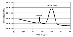
- the results of in-plane XRD analysis of the 3C-SiC single crystal epitaxial substrate obtained in the embodiment are shown.
- a large-diameter 3C-SiC freestanding substrate can be obtained by a simple manufacturing process using a manufacturing method for a 3C-SiC freestanding substrate, which includes a separation step of cooling the 3C-SiC single crystal epitaxial substrate manufactured by the manufacturing method described above, peeling off the 3C-SiC single crystal epitaxial substrate at the vacancy layer, and separating the 3C-SiC single crystal film from the single crystal silicon substrate to obtain a 3C-SiC freestanding substrate, and thus completed the present invention.
- a large-diameter 3C-SiC free-standing substrate can be obtained by a simple manufacturing process using a 3C-SiC single crystal epitaxial substrate comprising a single crystal silicon substrate and a 3C-SiC single crystal film of an epitaxial structure provided on the single crystal silicon substrate, the single crystal silicon substrate having a vacancy layer containing a collection of vacancies caused by missing Si at the interface with the 3C-SiC single crystal film, and thus completed the present invention.
- a 3C-SiC single crystal epitaxial substrate 1 includes a single crystal silicon substrate 3 and a 3C-SiC single crystal film 5 having an epitaxial structure provided on the single crystal silicon substrate.
- the single crystal silicon substrate 3 is a substrate that serves as the base when the 3C-SiC single crystal film 5 is formed by epitaxial growth.
- the thickness of the single crystal silicon substrate 3 depends on the thickness of the 3C-SiC single crystal film 5, but it is sufficient that the thickness is such that the single crystal silicon substrate 3 does not bend or crack due to stress caused by the difference in lattice constants between silicon and SiC when the 3C-SiC single crystal film 5 is formed by epitaxial growth.
- the single crystal silicon substrate 3 has a vacancy layer 7 containing a collection of vacancies generated by missing Si at the interface with the 3C-SiC single crystal film.
- the vacancy layer 7 is fragile compared to other portions due to the collection of vacancies, and therefore, by applying stress by cooling or the like, the 3C-SiC single crystal epitaxial substrate 1 can be peeled off at the vacancy layer 7, and the 3C-SiC single crystal film 5 can be easily separated from the single crystal silicon substrate 3. Therefore, the 3C-SiC single crystal epitaxial substrate 1 can be a large-diameter 3C-SiC free-standing substrate obtained by a simple manufacturing process.
- the portion of the single crystal silicon substrate 3 other than the vacancy layer 7 will be referred to as a base 11.
- the density of vacancies in the vacancy layer 7 and the thickness of the vacancy layer are appropriately set within a range that allows the 3C-SiC single crystal epitaxial substrate 1 to be easily peeled off by cooling.
- the 3C-SiC single crystal film 5 is a film having an epitaxial structure.
- the lower limit of the thickness of the 3C-SiC single crystal film 5 is a thickness that allows it to retain its shape without bending or cracking even after being separated from the single crystal silicon substrate 3, and that is not lost by polishing or etching during subsequent device formation.
- the upper limit of the thickness is a thickness that does not result in a large amount of unused portions during subsequent device formation, resulting in high costs.
- the diameter of the 3C-SiC single crystal film 5 is equal to or smaller than the diameter of the single crystal silicon substrate 3.
- a single crystal silicon substrate 3 is prepared as a base for epitaxial growth of the 3C-SiC single crystal film 5.
- the surface orientation of the prepared single crystal silicon substrate 3 is determined according to the surface orientation of the 3C-SiC single crystal film 5 to be grown, and is, for example, the (111) surface, but may also be the (110) surface or the (100) surface.
- the thickness of the single crystal silicon substrate 3 should be selected according to the thickness of the 3C-SiC single crystal film 5 to be grown so that it will not bend or break during growth.
- the diameter of the single crystal silicon substrate 3 should be equal to or larger than the diameter of the 3C-SiC single crystal film 5 to be grown.
- the prepared single crystal silicon substrate 3 is placed in a growth furnace for epitaxially growing the 3C-SiC single crystal film 5, such as an RP-CVD device (reduced pressure CVD device), and the single crystal silicon substrate 3 is H2 annealed in a hydrogen atmosphere to remove the natural oxide film on the surface (hydrogen bake step). If the natural oxide film remains, SiC nuclei cannot be formed when the 3C-SiC single crystal film 5 is epitaxially grown on the single crystal silicon substrate 3.
- a growth furnace for epitaxially growing the 3C-SiC single crystal film 5 such as an RP-CVD device (reduced pressure CVD device)
- the single crystal silicon substrate 3 is H2 annealed in a hydrogen atmosphere to remove the natural oxide film on the surface (hydrogen bake step). If the natural oxide film remains, SiC nuclei cannot be formed when the 3C-SiC single crystal film 5 is epitaxially grown on the single crystal silicon substrate 3.
- the H2 annealing temperature at this time is preferably set to 1000°C or higher and 1200°C or lower.
- the temperature at 1000°C or higher the hydrogen bake process for preventing the natural oxide film from remaining can be completed in a short time.
- the temperature at 1200°C or lower the occurrence of slip can be reliably suppressed.
- the surface of the single crystal silicon substrate 3 after the hydrogen bake process is carbonized to generate SiC nuclei, and the 3C-SiC single crystal film 5 is then grown heteroepitaxially from the generated nuclei (epitaxial process).
- a carbonizing gas such as propane gas is introduced into the RP-CVD apparatus as a raw material gas, while the temperature inside the apparatus is gradually increased from a range of 300°C to 950°C to a range of 1000°C to 1200°C.
- the source gas is switched to a gas containing C and Si, such as trimethylsilane gas, and the 3C-SiC single crystal film 5 is epitaxially grown starting from the nuclei generated by carbonization.
- the heating rate during epitaxial growth of SiC is preferably in the range of 0.5 to 5°C/min, and more preferably about 1°C/min.
- the thickness of the 3C-SiC single crystal film 5 grown in the epitaxial process may be thinner than the final target value. This is because the 3C-SiC single crystal film 5 will also be grown in a later process.
- the 3C-SiC single crystal epitaxial substrate is heated to a temperature below the melting point of Si in a carbon-containing gas atmosphere to cause the Si in the single crystal silicon substrate 3 to solid-state diffuse to the interface between the 3C-SiC single crystal film 5 and the single crystal silicon substrate 3, and the diffused Si reacts with the C that has reached the interface in a solid phase to further grow SiC, forming a vacancy layer 7 having vacancies that are generated at the site of the diffused Si at the interface between the single crystal silicon substrate 3 and the 3C-SiC single crystal film 5 (diffusion process).
- a solid-phase reaction causes vacancies at the interface between the single crystal silicon substrate 3 and the 3C-SiC single crystal film 5 after Si has been removed, and a collection of these vacancies forms the vacancy layer 7.
- the epitaxial process and the diffusion process can be performed without using a special pressure reducing device. Furthermore, by setting the pressure in the RP-CVD apparatus to 13332.2 Pa or less, the epitaxial growth of 3C-SiC in the epitaxial process and the diffusion of SiC in the diffusion process can be promoted. It is preferable to set the pressure in the RP-CVD apparatus in the diffusion step to about 666.612 Pa (5 Torr), since this promotes the growth of voids and increases the growth rate of SiC.
- the time for the diffusion step is the time required to obtain the 3C-SiC single crystal film 5 and void layer 7 of the desired thickness. The above is a description of the method for producing the 3C-SiC single crystal epitaxial substrate 1.
- the temperature drop at this time separates the 3C-SiC single crystal film 5 from the base 11 of the single crystal silicon substrate 3.
- the substrate is rapidly passed through a temperature range of around 400°C, the 3C-SiC single crystal epitaxial substrate 1 is rapidly peeled off starting from the vacancy layer 7, and the 3C-SiC single crystal film 5 is separated from the base 11 of the single crystal silicon substrate 3.
- the specific treatment for lowering the temperature is not particularly limited as long as it is possible to peel off the 3C-SiC single crystal epitaxial substrate 1 and separate the 3C-SiC single crystal film 5 from the single crystal silicon substrate 3, but examples include two treatments called a cooling process and a low-temperature treatment.
- the cooling process is a process in which, after the 3C-SiC single crystal film 5 of the desired predetermined thickness has grown, the 3C-SiC single crystal epitaxial substrate 1 is naturally cooled to 500°C, held at 500°C for 30 seconds to 3 minutes, and then cooled to 200°C at a rate of 4 to 5°C/min and removed.
- the 3C-SiC single crystal film 5 remains on the base 11 of the single crystal silicon substrate 3 even after peeling, it can be removed from the RP-CVD device as is, and after removal, the base 11 of the single crystal silicon substrate 3 and the 3C-SiC single crystal film 5 can be separated.
- the natural oxide film on the surface of a single crystal silicon substrate 3 with a diameter of, for example, 300 mm or more is removed in a hydrogen bake process, followed by a carbonization process, after which heteroepitaxial growth of a 3C-SiC single crystal film 5 is performed on the single crystal silicon substrate 3, and then the temperature is raised to a level that does not melt the single crystal silicon substrate 3, a gas containing carbon is passed through it, and the 3C-SiC single crystal film 5 is further grown by solid diffusion of the single crystal silicon substrate 3, producing a 3C-SiC epitaxial substrate with numerous pores at the interface between the single crystal silicon substrate 3 and the 3C-SiC single crystal film 5, and these pores can be used to perform peeling in a subsequent cooling process, etc.
- the temperature in the furnace was lowered to 300°C, and then propane gas was introduced to form SiC nuclei while raising the temperature to 1130°C at a heating rate of 1°C/sec, and trimethylsilane gas was further introduced to form the subsequent 3C-SiC single crystal film 5.
- the growth pressure at this time was uniformly set to 666.612 Pa (5 Torr).
- the temperature inside the reactor reached 1130°C, it was maintained for 10 hours, and as a diffusion process, the 3C-SiC single crystal film 5 was grown and the pore layer 7 was formed.
- the thickness of the 3C-SiC single crystal film 5 reached 100 ⁇ m, the supply of the raw material gas was stopped and the film was naturally cooled to 500°C, maintained at 500°C for 120 seconds, and then cooled to 200°C at 5°C/min (cooling process).
Landscapes
- Chemical & Material Sciences (AREA)
- Metallurgy (AREA)
- Engineering & Computer Science (AREA)
- Materials Engineering (AREA)
- Organic Chemistry (AREA)
- Crystallography & Structural Chemistry (AREA)
- General Chemical & Material Sciences (AREA)
- Chemical Kinetics & Catalysis (AREA)
- Mechanical Engineering (AREA)
- Inorganic Chemistry (AREA)
- Physics & Mathematics (AREA)
- Thermal Sciences (AREA)
- Crystals, And After-Treatments Of Crystals (AREA)
- Chemical Vapour Deposition (AREA)
Abstract
Description
そのため、簡易な製造プロセスによって、大口径3C-SiC自立基板を得ることができる。
そのため、簡易な製造プロセスによって、大口径3C-SiC自立基板を得ることができる。
そのため、簡易な製造プロセスによって、大口径3C-SiC自立基板を得ることができるものとなる。
また、本発明の3C-SiC自立基板の製造方法によれば、簡易な製造プロセスによって、大口径3C-SiC自立基板を得ることが可能となる。
さらに、本発明の3C-SiC単結晶エピタキシャル基板によれば、簡易な製造プロセスによって、大口径3C-SiC自立基板を得ることが可能なものとなる。
以下、図1及び図2を参照しながら本発明の実施形態に係る3C-SiC単結晶エピタキシャル基板1の製造方法、3C-SiC自立基板9の製造方法、及び3C-SiC単結晶エピタキシャル基板1の構成について説明する。
図1に示すように3C-SiC単結晶エピタキシャル基板1は単結晶シリコン基板3と、単結晶シリコン基板上に設けられたエピタキシャル構造の3C-SiC単結晶膜5を備える。
空孔層7は空孔の集合があるため、他の部分と比べて脆くなっている。そのため冷却等で応力を加えることで、空孔層7で3C-SiC単結晶エピタキシャル基板1を剥離して単結晶シリコン基板3から3C-SiC単結晶膜5を容易に分離できるものとなる。
よって、3C-SiC単結晶エピタキシャル基板1は、簡易な製造プロセスによって、大口径3C-SiC自立基板を得ることができるものとなる。
なお、単結晶シリコン基板3における空孔層7以外の部分を以下の説明では基部11と称す。また、空孔層7における空孔の密度や空孔層の厚さは、冷却で容易に3C-SiC単結晶エピタキシャル基板1を剥離できる範囲で適宜設定する。
なお、拡散工程におけるRP-CVD装置内の圧力を666.612Pa(5Torr.)程度の圧力にすると、空孔の成長が促進され、かつSiCの成長速度も大きくなるので、好ましい。また、拡散工程の時間は、所望の厚さの3C-SiC単結晶膜5と空孔層7が得られる時間である。
以上が3C-SiC単結晶エピタキシャル基板1の製造方法の説明である。
冷却過程とは、目標とする所定の厚さの3C-SiC単結晶膜5が成長した後に3C-SiC単結晶エピタキシャル基板1を500℃まで自然冷却し、500℃で30秒~3分保持し、200℃まで4~5℃/minで冷却し取り出す処理である。
低温処理とは、目標とする所定の厚さの3C-SiC単結晶膜5が成長した後に3C-SiC単結晶エピタキシャル基板1を200℃の炉内に直接投入し、200℃にて2時間処理後、4~5℃/minで500℃まで昇温し、500℃にて30秒保持し、そのまま炉外に取り出し室温にて自然冷却する処理である。
以上が3C-SiC自立基板9の製造方法の説明である。
本発明の3C-SiC単結晶エピタキシャル基板の製造方法で3C-SiC単結晶エピタキシャル基板1を製造し、さらに3C-SiC自立基板9の製造を試みた。具体的な手順は以下の通りである。
次にRP‐CVD装置の反応炉内のサセプター上にウェーハを配置し、水素ベイク工程として、1080℃で1分間のH2アニールを行った。続いて、エピタキシャル工程として、炉内温度を300℃まで降温させた後、昇温レート1℃/secで1130度まで昇温させながらプロパンガスを導入してSiCの核形成を行い、さらにトリメチルシランガスを導入してそれに続く3C-SiC単結晶膜5の形成を行った。この時の成長圧力は一律666.612Pa(5Torr)とした。
Claims (4)
- 単結晶シリコン基板を水素雰囲気下でアニールすることで前記単結晶シリコン基板の表面の自然酸化膜を除去する水素ベイク工程と、
前記水素ベイク工程後の前記単結晶シリコン基板の表面に炭化処理を行いSiCの核を生成し、さらに生成した核を起点に3C-SiC単結晶膜をエピタキシャル成長させて3C-SiC単結晶エピタキシャル基板を得るエピタキシャル工程と、
前記3C-SiC単結晶エピタキシャル基板を、炭素を含むガス雰囲気下でSiの融点未満の温度に加熱して前記単結晶シリコン基板中のSiを前記3C-SiC単結晶膜と前記単結晶シリコン基板との界面まで固体拡散させ、該拡散させたSiと前記界面に到達したCとの固相反応で、さらにSiCを成長させることで、Siが拡散した跡に生じる空孔を有する空孔層を前記単結晶シリコン基板における前記3C-SiC単結晶膜との前記界面に形成する拡散工程と、
を含むことを特徴とする3C-SiC単結晶エピタキシャル基板の製造方法。 - 前記エピタキシャル工程及び前記拡散工程を、133.322Pa以上、13332.2Pa以下の圧力範囲で行うことを特徴とする請求項1に記載の3C-SiC単結晶エピタキシャル基板の製造方法。
- 請求項1又は2に記載の3C-SiC単結晶エピタキシャル基板の製造方法で製造された前記3C-SiC単結晶エピタキシャル基板を冷却することで、前記空孔層で前記3C-SiC単結晶エピタキシャル基板を剥離し、前記単結晶シリコン基板から前記3C-SiC単結晶膜を分離して3C-SiC自立基板とする分離工程を含むことを特徴とする3C-SiC自立基板の製造方法。
- 単結晶シリコン基板と、
前記単結晶シリコン基板上に設けられたエピタキシャル構造の3C-SiC単結晶膜と、
を備え、
前記単結晶シリコン基板は、
Siが欠落して生じた空孔の集合を含む空孔層を前記3C-SiC単結晶膜との界面に有することを特徴とする3C-SiC単結晶エピタキシャル基板。
Priority Applications (3)
| Application Number | Priority Date | Filing Date | Title |
|---|---|---|---|
| CN202380090205.0A CN120418486A (zh) | 2023-01-19 | 2023-10-03 | 3C-SiC单晶外延基板的制造方法、3C-SiC自支撑基板的制造方法及3C-SiC单晶外延基板 |
| EP23917604.3A EP4653588A1 (en) | 2023-01-19 | 2023-10-03 | Method for manufacturing 3c-sic single-crystal epitaxial substrate, method for manufacturing 3c-sic free-standing substrate, and 3c-sic single-crystal epitaxial substrate |
| KR1020257023100A KR20250135787A (ko) | 2023-01-19 | 2023-10-03 | 3C-SiC 단결정 에피택셜 기판의 제조방법, 3C-SiC 자립기판의 제조방법, 및 3C-SiC 단결정 에피택셜 기판 |
Applications Claiming Priority (2)
| Application Number | Priority Date | Filing Date | Title |
|---|---|---|---|
| JP2023006762A JP2024102694A (ja) | 2023-01-19 | 2023-01-19 | 3C-SiC単結晶エピタキシャル基板の製造方法、3C-SiC自立基板の製造方法、及び3C-SiC単結晶エピタキシャル基板 |
| JP2023-006762 | 2023-03-31 |
Publications (1)
| Publication Number | Publication Date |
|---|---|
| WO2024154392A1 true WO2024154392A1 (ja) | 2024-07-25 |
Family
ID=91955770
Family Applications (1)
| Application Number | Title | Priority Date | Filing Date |
|---|---|---|---|
| PCT/JP2023/035983 Ceased WO2024154392A1 (ja) | 2023-01-19 | 2023-10-03 | 3C-SiC単結晶エピタキシャル基板の製造方法、3C-SiC自立基板の製造方法、及び3C-SiC単結晶エピタキシャル基板 |
Country Status (6)
| Country | Link |
|---|---|
| EP (1) | EP4653588A1 (ja) |
| JP (1) | JP2024102694A (ja) |
| KR (1) | KR20250135787A (ja) |
| CN (1) | CN120418486A (ja) |
| TW (1) | TW202432913A (ja) |
| WO (1) | WO2024154392A1 (ja) |
Families Citing this family (1)
| Publication number | Priority date | Publication date | Assignee | Title |
|---|---|---|---|---|
| JP2026058227A (ja) * | 2024-09-24 | 2026-04-03 | 信越半導体株式会社 | ヘテロエピタキシャルウェーハ及びその製造方法 |
Citations (7)
| Publication number | Priority date | Publication date | Assignee | Title |
|---|---|---|---|---|
| JPH11162850A (ja) | 1997-08-27 | 1999-06-18 | Matsushita Electric Ind Co Ltd | 炭化珪素基板およびその製造方法、並びに炭化珪素基板を用いた半導体素子 |
| JP2006253617A (ja) | 2005-02-14 | 2006-09-21 | Toshiba Ceramics Co Ltd | SiC半導体およびその製造方法 |
| JP2008184361A (ja) | 2007-01-30 | 2008-08-14 | Covalent Materials Corp | 3C−SiC単結晶膜の形成方法 |
| US20130157448A1 (en) | 2011-12-15 | 2013-06-20 | Stmicroelectronics S.R.L. | Method for manufacturing a silicon carbide wafer and respective equipment |
| JP2017039622A (ja) | 2015-08-19 | 2017-02-23 | エア・ウォーター株式会社 | 化合物半導体基板および化合物半導体基板の製造方法 |
| JP2019014628A (ja) * | 2017-07-07 | 2019-01-31 | セイコーエプソン株式会社 | 炭化ケイ素膜付き基板の製造方法、炭化ケイ素膜付き基板および炭化ケイ素単結晶基板 |
| JP2021020819A (ja) | 2019-07-24 | 2021-02-18 | 株式会社Sumco | ヘテロエピタキシャルウェーハの製造方法及びヘテロエピタキシャルウェーハ |
Family Cites Families (1)
| Publication number | Priority date | Publication date | Assignee | Title |
|---|---|---|---|---|
| US10907273B2 (en) | 2015-07-23 | 2021-02-02 | The University Of Warwick | Growing epitaxial 3C-SiC on single-crystal silicon |
-
2023
- 2023-01-19 JP JP2023006762A patent/JP2024102694A/ja active Pending
- 2023-10-03 CN CN202380090205.0A patent/CN120418486A/zh active Pending
- 2023-10-03 WO PCT/JP2023/035983 patent/WO2024154392A1/ja not_active Ceased
- 2023-10-03 KR KR1020257023100A patent/KR20250135787A/ko active Pending
- 2023-10-03 EP EP23917604.3A patent/EP4653588A1/en active Pending
- 2023-10-04 TW TW112138066A patent/TW202432913A/zh unknown
Patent Citations (8)
| Publication number | Priority date | Publication date | Assignee | Title |
|---|---|---|---|---|
| JPH11162850A (ja) | 1997-08-27 | 1999-06-18 | Matsushita Electric Ind Co Ltd | 炭化珪素基板およびその製造方法、並びに炭化珪素基板を用いた半導体素子 |
| JP2006253617A (ja) | 2005-02-14 | 2006-09-21 | Toshiba Ceramics Co Ltd | SiC半導体およびその製造方法 |
| JP2008184361A (ja) | 2007-01-30 | 2008-08-14 | Covalent Materials Corp | 3C−SiC単結晶膜の形成方法 |
| US20130157448A1 (en) | 2011-12-15 | 2013-06-20 | Stmicroelectronics S.R.L. | Method for manufacturing a silicon carbide wafer and respective equipment |
| US20160307800A1 (en) | 2011-12-15 | 2016-10-20 | Stmicroelectronics S.R.L. | Method for manufacturing a silicon carbide wafer and respective equipment |
| JP2017039622A (ja) | 2015-08-19 | 2017-02-23 | エア・ウォーター株式会社 | 化合物半導体基板および化合物半導体基板の製造方法 |
| JP2019014628A (ja) * | 2017-07-07 | 2019-01-31 | セイコーエプソン株式会社 | 炭化ケイ素膜付き基板の製造方法、炭化ケイ素膜付き基板および炭化ケイ素単結晶基板 |
| JP2021020819A (ja) | 2019-07-24 | 2021-02-18 | 株式会社Sumco | ヘテロエピタキシャルウェーハの製造方法及びヘテロエピタキシャルウェーハ |
Non-Patent Citations (5)
| Title |
|---|
| ASAMURA ET AL.: "The 62nd Spring Meeting of the Japan Society of Applied Physics", 2015, THE JAPAN SOCIETY OF APPLIED PHYSICS, article "Crystal Quality of Free-Standing 3C-SiC(111) Substrates by Low Temperature Growth", pages: 13 - 095 |
| D. CHAUSSENDEF. MERCIERA. BOULLEF. CONCHONM. SOUEIDANG. FERROA. MANTZARIA. ANDREADOUE. K. POLYCHRONIADISC. BALLOUD: "Prospects for 3C-SiC bulk crystal growth", JOURNAL OF CRYSTAL GROWTH, vol. 310, 2008, pages 976, XP022492835 |
| H. NAGASAWAK. YAGIT. KAWAHARA: "3C-SiC hetero-epitaxial growth on undulant Si(001) substrate", JOURNAL OF CRYSTAL GROWTH, vol. 239, 2002, pages 1244 |
| See also references of EP4653588A1 |
| T. UJIHARAR. MAEKAWAR. TANAKAK. SASAKIK. KURODAY. TAKEDA: "Solution growth of high-quality 3C-SiC crystals", JOURNAL OF CRYSTAL GROWTH, vol. 310, 2008, pages 1438 |
Also Published As
| Publication number | Publication date |
|---|---|
| EP4653588A1 (en) | 2025-11-26 |
| KR20250135787A (ko) | 2025-09-15 |
| CN120418486A (zh) | 2025-08-01 |
| JP2024102694A (ja) | 2024-07-31 |
| TW202432913A (zh) | 2024-08-16 |
Similar Documents
| Publication | Publication Date | Title |
|---|---|---|
| CN101553604B (zh) | 碳化硅单晶的制造方法 | |
| JP5896038B2 (ja) | ナノカーボン膜の作製方法 | |
| JP7259906B2 (ja) | ヘテロエピタキシャルウェーハの製造方法 | |
| JP5542383B2 (ja) | シリコンウェーハの熱処理方法 | |
| JP2024102694A (ja) | 3C-SiC単結晶エピタキシャル基板の製造方法、3C-SiC自立基板の製造方法、及び3C-SiC単結晶エピタキシャル基板 | |
| JP3312553B2 (ja) | シリコン単結晶およびシリコン単結晶薄膜の製造方法 | |
| JP2006253617A (ja) | SiC半導体およびその製造方法 | |
| JP4987784B2 (ja) | 炭化珪素単結晶インゴットの製造方法 | |
| JP4511378B2 (ja) | SOI基板を用いた単結晶SiC層を形成する方法 | |
| JP7218832B1 (ja) | ヘテロエピタキシャルウェーハの製造方法 | |
| JP7708198B2 (ja) | ヘテロエピタキシャル膜の作製方法 | |
| JP2009190953A (ja) | 半導体基板の製造方法およびそれによって製造される半導体基板 | |
| JP2010225733A (ja) | 半導体基板の製造方法 | |
| EP4567165A1 (en) | Method for manufacturing 3c-sic laminated substrate, 3c-sic laminated substrate, and 3c-sic independent substrate | |
| WO2025134577A1 (ja) | ヘテロエピタキシャルウェーハの製造方法 | |
| JP2010225734A (ja) | 半導体基板の製造方法 | |
| JP2007261900A (ja) | 単結晶炭化シリコン基板の製造方法 | |
| JP2026056867A (ja) | 半導体基板及びその製造方法 | |
| JP2007095800A (ja) | 半導体基板の製造方法 | |
| JP2009302097A (ja) | 単結晶SiC基板の製造方法および単結晶SiC基板 | |
| JP2006245054A (ja) | 多層のエピタキシャルシリコン単結晶ウェーハの製造方法及び多層のエピタキシャルシリコン単結晶ウェーハ | |
| JP2007273525A (ja) | 立方晶系単結晶炭化シリコン基板の製造方法 |
Legal Events
| Date | Code | Title | Description |
|---|---|---|---|
| 121 | Ep: the epo has been informed by wipo that ep was designated in this application |
Ref document number: 23917604 Country of ref document: EP Kind code of ref document: A1 |
|
| WWE | Wipo information: entry into national phase |
Ref document number: 202380090205.0 Country of ref document: CN |
|
| ENP | Entry into the national phase |
Ref document number: 1020257023100 Country of ref document: KR Free format text: ST27 STATUS EVENT CODE: A-0-1-A10-A15-NAP-PA0105 (AS PROVIDED BY THE NATIONAL OFFICE) |
|
| WWP | Wipo information: published in national office |
Ref document number: 202380090205.0 Country of ref document: CN |
|
| NENP | Non-entry into the national phase |
Ref country code: DE |
|
| WWP | Wipo information: published in national office |
Ref document number: 2023917604 Country of ref document: EP |