WO2024143061A1 - メタルマスク用基材、メタルマスク、および、メタルマスクの製造方法 - Google Patents
メタルマスク用基材、メタルマスク、および、メタルマスクの製造方法 Download PDFInfo
- Publication number
- WO2024143061A1 WO2024143061A1 PCT/JP2023/045440 JP2023045440W WO2024143061A1 WO 2024143061 A1 WO2024143061 A1 WO 2024143061A1 JP 2023045440 W JP2023045440 W JP 2023045440W WO 2024143061 A1 WO2024143061 A1 WO 2024143061A1
- Authority
- WO
- WIPO (PCT)
- Prior art keywords
- metal mask
- mass
- mask substrate
- less
- holes
- Prior art date
- Legal status (The legal status is an assumption and is not a legal conclusion. Google has not performed a legal analysis and makes no representation as to the accuracy of the status listed.)
- Ceased
Links
Images




Classifications
-
- C—CHEMISTRY; METALLURGY
- C23—COATING METALLIC MATERIAL; COATING MATERIAL WITH METALLIC MATERIAL; CHEMICAL SURFACE TREATMENT; DIFFUSION TREATMENT OF METALLIC MATERIAL; COATING BY VACUUM EVAPORATION, BY SPUTTERING, BY ION IMPLANTATION OR BY CHEMICAL VAPOUR DEPOSITION, IN GENERAL; INHIBITING CORROSION OF METALLIC MATERIAL OR INCRUSTATION IN GENERAL
- C23C—COATING METALLIC MATERIAL; COATING MATERIAL WITH METALLIC MATERIAL; SURFACE TREATMENT OF METALLIC MATERIAL BY DIFFUSION INTO THE SURFACE, BY CHEMICAL CONVERSION OR SUBSTITUTION; COATING BY VACUUM EVAPORATION, BY SPUTTERING, BY ION IMPLANTATION OR BY CHEMICAL VAPOUR DEPOSITION, IN GENERAL
- C23C14/00—Coating by vacuum evaporation, by sputtering or by ion implantation of the coating forming material
- C23C14/04—Coating on selected surface areas, e.g. using masks
- C23C14/042—Coating on selected surface areas, e.g. using masks using masks
-
- C—CHEMISTRY; METALLURGY
- C22—METALLURGY; FERROUS OR NON-FERROUS ALLOYS; TREATMENT OF ALLOYS OR NON-FERROUS METALS
- C22C—ALLOYS
- C22C38/00—Ferrous alloys, e.g. steel alloys
- C22C38/04—Ferrous alloys, e.g. steel alloys containing manganese
-
- C—CHEMISTRY; METALLURGY
- C22—METALLURGY; FERROUS OR NON-FERROUS ALLOYS; TREATMENT OF ALLOYS OR NON-FERROUS METALS
- C22C—ALLOYS
- C22C38/00—Ferrous alloys, e.g. steel alloys
- C22C38/08—Ferrous alloys, e.g. steel alloys containing nickel
-
- C—CHEMISTRY; METALLURGY
- C23—COATING METALLIC MATERIAL; COATING MATERIAL WITH METALLIC MATERIAL; CHEMICAL SURFACE TREATMENT; DIFFUSION TREATMENT OF METALLIC MATERIAL; COATING BY VACUUM EVAPORATION, BY SPUTTERING, BY ION IMPLANTATION OR BY CHEMICAL VAPOUR DEPOSITION, IN GENERAL; INHIBITING CORROSION OF METALLIC MATERIAL OR INCRUSTATION IN GENERAL
- C23C—COATING METALLIC MATERIAL; COATING MATERIAL WITH METALLIC MATERIAL; SURFACE TREATMENT OF METALLIC MATERIAL BY DIFFUSION INTO THE SURFACE, BY CHEMICAL CONVERSION OR SUBSTITUTION; COATING BY VACUUM EVAPORATION, BY SPUTTERING, BY ION IMPLANTATION OR BY CHEMICAL VAPOUR DEPOSITION, IN GENERAL
- C23C14/00—Coating by vacuum evaporation, by sputtering or by ion implantation of the coating forming material
- C23C14/04—Coating on selected surface areas, e.g. using masks
-
- C—CHEMISTRY; METALLURGY
- C23—COATING METALLIC MATERIAL; COATING MATERIAL WITH METALLIC MATERIAL; CHEMICAL SURFACE TREATMENT; DIFFUSION TREATMENT OF METALLIC MATERIAL; COATING BY VACUUM EVAPORATION, BY SPUTTERING, BY ION IMPLANTATION OR BY CHEMICAL VAPOUR DEPOSITION, IN GENERAL; INHIBITING CORROSION OF METALLIC MATERIAL OR INCRUSTATION IN GENERAL
- C23C—COATING METALLIC MATERIAL; COATING MATERIAL WITH METALLIC MATERIAL; SURFACE TREATMENT OF METALLIC MATERIAL BY DIFFUSION INTO THE SURFACE, BY CHEMICAL CONVERSION OR SUBSTITUTION; COATING BY VACUUM EVAPORATION, BY SPUTTERING, BY ION IMPLANTATION OR BY CHEMICAL VAPOUR DEPOSITION, IN GENERAL
- C23C14/00—Coating by vacuum evaporation, by sputtering or by ion implantation of the coating forming material
- C23C14/22—Coating by vacuum evaporation, by sputtering or by ion implantation of the coating forming material characterised by the process of coating
- C23C14/24—Vacuum evaporation
-
- H—ELECTRICITY
- H05—ELECTRIC TECHNIQUES NOT OTHERWISE PROVIDED FOR
- H05B—ELECTRIC HEATING; ELECTRIC LIGHT SOURCES NOT OTHERWISE PROVIDED FOR; CIRCUIT ARRANGEMENTS FOR ELECTRIC LIGHT SOURCES, IN GENERAL
- H05B33/00—Electroluminescent light sources
- H05B33/10—Apparatus or processes specially adapted to the manufacture of electroluminescent light sources
-
- H—ELECTRICITY
- H10—SEMICONDUCTOR DEVICES; ELECTRIC SOLID-STATE DEVICES NOT OTHERWISE PROVIDED FOR
- H10K—ORGANIC ELECTRIC SOLID-STATE DEVICES
- H10K50/00—Organic light-emitting devices
- H10K50/10—OLEDs or polymer light-emitting diodes [PLED]
-
- H—ELECTRICITY
- H10—SEMICONDUCTOR DEVICES; ELECTRIC SOLID-STATE DEVICES NOT OTHERWISE PROVIDED FOR
- H10K—ORGANIC ELECTRIC SOLID-STATE DEVICES
- H10K71/00—Manufacture or treatment specially adapted for the organic devices covered by this subclass
- H10K71/10—Deposition of organic active material
- H10K71/16—Deposition of organic active material using physical vapour deposition [PVD], e.g. vacuum deposition or sputtering
-
- H—ELECTRICITY
- H10—SEMICONDUCTOR DEVICES; ELECTRIC SOLID-STATE DEVICES NOT OTHERWISE PROVIDED FOR
- H10K—ORGANIC ELECTRIC SOLID-STATE DEVICES
- H10K71/00—Manufacture or treatment specially adapted for the organic devices covered by this subclass
- H10K71/10—Deposition of organic active material
- H10K71/16—Deposition of organic active material using physical vapour deposition [PVD], e.g. vacuum deposition or sputtering
- H10K71/166—Deposition of organic active material using physical vapour deposition [PVD], e.g. vacuum deposition or sputtering using selective deposition, e.g. using a mask
Definitions
- This disclosure relates to a metal mask substrate, a metal mask, and a method for manufacturing a metal mask.
- One example of a method for forming pixels in an organic EL display device is the vacuum deposition method.
- a metal deposition mask with multiple through holes is used.
- Each through hole has a shape corresponding to the shape of a pixel, and the multiple through holes are arranged according to the arrangement of the pixels.
- Each through hole is a passage through which the deposition material for forming the pixels passes.
- a metal thin plate made of an iron-nickel alloy is used as the material for forming the deposition mask (see, for example, Patent Document 1).
- a deposition mask from a thin metal sheet When manufacturing a deposition mask from a thin metal sheet, first a resist layer is formed on the surface of the thin metal sheet, and then a resist pattern is formed from the resist layer. Then, multiple through holes are formed in the thin metal sheet by wet etching using the resist pattern.
- the metal mask substrate for solving the above problem is a metal mask substrate whose main component is an iron-nickel alloy, contains 0.25% by mass or more and 0.40% by mass or less of manganese element, and has a thickness of 50 ⁇ m or less.
- the metal mask substrate contains 0.25 mass% or more of manganese, which has a lower standard electrode potential than iron and nickel. Therefore, the metal mask substrate is in a state in which it is susceptible to corrosion, and the corrosion potential that occurs when the etching solution comes into contact with the metal mask substrate is low, making it less likely that pitting corrosion will occur when the metal mask substrate comes into contact with the etching solution. As a result, excessive wet etching is prevented from progressing locally in the metal mask substrate, and some of the multiple through holes are prevented from becoming larger.
- the metal mask substrate may contain 0.03% by mass or more and 0.05% by mass or less of silicon element. With this metal mask substrate, the metal mask substrate contains 0.03% by mass or more and 0.05% by mass or less of silicon element, so galvanic corrosion between the silicon element and metal elements located in the vicinity is suppressed, which further suppresses some of the through holes from becoming larger.
- the metal mask substrate contains 63.5% by mass to 64.5% by mass of iron element, 35.0% by mass to 36.5% by mass of nickel element, and 0.29% by mass to 0.7% by mass of an additive element, which may include the manganese element.
- the iron content, nickel content, and additive element content all satisfy the above-mentioned ranges, so the effectiveness of the manganese content being 0.25 mass% or more and 0.40 mass% or less is enhanced.
- the metal mask for solving the above problem is a metal mask formed from a metal mask substrate mainly composed of an iron-nickel alloy, containing 0.25% by mass to 0.40% by mass of manganese element, having a maximum thickness of 50 ⁇ m or less, and including a first surface and a plurality of through holes having openings in the first surface, the area of the openings being 1600 ⁇ m or less.
- the metal mask substrate contains 0.25 mass % or more of manganese, which has a lower standard electrode potential than iron and nickel. Therefore, the metal mask substrate is in a state where it is easily corroded, and the corrosion potential generated when the etching solution contacts the metal mask substrate is low, so that pitting corrosion is unlikely to occur when the metal mask substrate contacts the etching solution. As a result, even when forming through holes with a fine opening of 1600 ⁇ m2 or less, excessive wet etching is prevented from progressing locally in the metal mask substrate, and some of the through holes among the plurality of through holes are prevented from becoming large.
- the metal mask may include an oxide layer containing an oxide of the iron-nickel alloy, and the oxide layer may include the first surface.
- the metal mask since the metal mask includes an oxide layer, pitting corrosion is likely to occur in the metal mask substrate used to form the metal mask when the through holes in the metal mask are formed. This enhances the effectiveness of the metal mask substrate having a manganese content of 0.25 mass% or more and 0.40 mass% or less, which has a lower standard electrode potential than iron and nickel.
- a method for manufacturing a metal mask for solving the above problems includes forming a plurality of through holes by wet etching in a metal mask substrate having a thickness of 50 ⁇ m or less, the substrate containing 0.25 mass % or more and 0.40 mass % or less manganese element, and an iron-nickel alloy as a main component, the substrate having a first surface, the thickness of the substrate being 50 ⁇ m or less, and the forming of the plurality of through holes includes forming a through hole having an opening in the first surface, the opening having an area of 1600 ⁇ m2 or less.
- the metal mask substrate contains 0.25 mass % or more of manganese, which has a lower standard electrode potential than iron and nickel. Therefore, the metal mask substrate is in a state where it is easily corroded, and the corrosion potential generated when the etching solution contacts the metal mask substrate is low, so that pitting corrosion is unlikely to occur when the metal mask substrate contacts the etching solution. As a result, even when forming through holes with a fine opening of 1600 ⁇ m2 or less, excessive wet etching is prevented from progressing locally in the metal mask substrate, and some of the through holes among the plurality of through holes are prevented from becoming large.
- forming the plurality of through holes may include forming the plurality of through holes by wet etching the metal mask substrate using a ferric chloride solution having a specific gravity of 47° Baume or more and 52° Baume or less.
- the above-mentioned method for manufacturing a metal mask prevents pitting corrosion from occurring when forming through holes in the metal mask substrate, even when a ferric chloride solution containing chloride ions that cause pitting corrosion is used as the etching solution.
- forming the plurality of through holes may include forming a resist pattern on the first surface, and the contact angle of the resist pattern with the etching solution may be 40° or less. This method for manufacturing a metal mask allows for greater freedom in the thickness of the resist pattern.
- the above-mentioned metal mask substrate, metal mask, and method for manufacturing a metal mask prevent some of the through holes in the metal mask from becoming larger.
- FIG. 1 is a perspective view showing a metal mask substrate.
- FIG. 2 is a cross-sectional view of the metal mask substrate shown in FIG.
- FIG. 3 is a process diagram showing a process in which excessive wet etching progresses locally in a metal mask substrate.
- FIG. 4 is a process diagram showing a process in which excessive wet etching progresses locally on a metal mask substrate.
- FIG. 5 is a process diagram showing a process in which excessive wet etching progresses locally in a metal mask substrate.
- FIG. 6 is a schematic diagram for explaining pitting corrosion that occurs in a metal mask substrate.
- FIG. 7 is a process diagram showing a process in which excessive wet etching progresses locally in a metal mask substrate.
- FIG. 1 is a perspective view showing a metal mask substrate.
- FIG. 2 is a cross-sectional view of the metal mask substrate shown in FIG.
- FIG. 3 is a process diagram showing a process in which excessive wet etching
- FIG. 8 is a plan view showing the metal mask.
- FIG. 9 is an enlarged plan view of a portion of the metal mask shown in FIG.
- FIG. 10 is a cross-sectional view showing a first example of the structure of the metal mask shown in FIG.
- FIG. 11 is a cross-sectional view showing a second example of the structure of the metal mask shown in FIG.
- FIG. 12 is a process diagram showing one step included in the method for manufacturing a metal mask.
- FIG. 13 is a process diagram showing one step included in the method for manufacturing a metal mask.
- FIG. 14 is a process diagram showing one step included in the method for manufacturing a metal mask.
- FIG. 15 is a process diagram showing one step included in the method for manufacturing a metal mask.
- FIG. 15 is a process diagram showing one step included in the method for manufacturing a metal mask.
- FIG. 16 is a process diagram showing one step included in the method for manufacturing a metal mask.
- FIG. 17 is a process diagram showing one step included in the method for manufacturing a metal mask.
- FIG. 18 is a table showing the results of composition analysis of the metal mask substrates of the examples and comparative examples, and the incidence of recess expansion.
- FIG. 19 is a graph showing the relationship between the incidence of recess expansion and the manganese element content when a metal mask substrate is wet-etched using a 47° Baume ferric chloride solution.
- FIG. 20 is a graph showing the relationship between the incidence of recess expansion and the manganese element content when a metal mask substrate is wet-etched using a 50° Baume ferric chloride solution.
- FIG. 21 is a graph showing the relationship between the predicted value of the incidence rate of recess expansion calculated based on the prediction formula for manganese element and the actual measured value of the incidence rate of recess expansion.
- FIG. 22 is a graph showing the relationship between the predicted values of the incidence rate of recess expansion calculated based on the prediction formula for manganese element and silicon element and the actually measured values of the incidence rate of recess expansion.
- FIG. 23 is a graph showing the relationship between etching depth and the incidence rate of recess expansion.
- FIG. 24 is an SEM image of a portion of the metal mask substrate where excessive wet etching has not progressed locally.
- FIG. 25 is an SEM image of a portion of the metal mask substrate where excessive wet etching has progressed locally.
- FIG. 26 is a SEM image of a portion of the metal mask substrate where localized excessive wet etching has not progressed and a portion where localized excessive etching has progressed.
- FIG. 27 is a graph showing the relationship between the contact angle of the resist pattern and the incidence rate of recess expansion when the resist pattern has a thickness of 10 ⁇ m.
- FIG. 28 is a graph showing the relationship between the contact angle of the resist pattern and the incidence rate of recess expansion when the resist pattern has a thickness of 5 ⁇ m.
- the metal mask substrate will be described with reference to FIG. 1 and FIG. 1 is made primarily of an iron-nickel alloy (Fe-Ni alloy).
- the metal mask substrate 10 contains 0.25% by mass to 0.40% by mass of manganese (Mn) and has a thickness T of 50 ⁇ m or less.
- the metal mask substrate 10 may contain 0.03% by mass or more and 0.05% by mass or less of silicon (Si).
- the metal mask substrate 10 may contain 63.5% by mass or more and 64.5% by mass or less of iron (Fe), 35.0% by mass or more and 36.5% by mass or less of nickel (Ni), and 0.29% by mass or more and 0.7% by mass or less of an additive element.
- the additive element is an element other than iron and nickel, which are the main components of the metal mask substrate 10.
- the additive element includes the above-mentioned manganese element.
- Manganese is added as a deoxidizing agent to the iron-nickel alloy in the manufacturing process of the metal mask substrate 10 to deoxidize the iron-nickel alloy.
- manganese as a deoxidizing agent instead of aluminum and magnesium, the inclusion of spinel (MgAl 2 O 4 ) in the metal mask substrate 10 is suppressed.
- the manganese content in the metal mask substrate 10 increases, the manganese tends to segregate.
- Silicon like manganese, deoxidizes iron-nickel alloys, so it is added as a deoxidizer to iron-nickel alloys during the manufacturing process of metal mask substrate 10.
- silicon as a deoxidizer instead of aluminum and magnesium, the inclusion of spinel in metal mask substrate 10 is suppressed.
- the silicon content in metal mask substrate 10 increases, the silicon is more likely to segregate.
- the additive elements may include metal elements other than manganese and nonmetal elements.
- Metal elements may be, for example, magnesium (Mg), aluminum (Al), chromium (Cr), molybdenum (Mo), and cobalt (Co).
- Nonmetal elements may be the above-mentioned silicon, phosphorus (P), sulfur (S), and chlorine (Cl).
- the magnesium element content may be, for example, 0.000% by mass or more and 0.007% by mass or less.
- the aluminum element content may be, for example, 0.003% by mass or more and 0.029% by mass or less.
- the chromium element content may be, for example, 0.004% by mass or more and 0.046% by mass or less.
- the molybdenum element content may be, for example, 0.000% by mass or more and 0.010% by mass or less.
- the cobalt element content may be, for example, 0.000% by mass or more and 0.265% by mass or less.
- the ingot is subjected to a rolling process or the like to obtain the metal mask substrate 10.
- the rolling process may be at least one of hot rolling and cold rolling. That is, the ingot may be subjected to only one of hot rolling and cold rolling, or may be subjected to both hot rolling and cold rolling.
- the metal mask substrate 10 has a band shape including a front surface 10F and a back surface 10R, which is the surface opposite to the front surface 10F.
- the thickness T of the metal mask substrate 10 is the distance between the front surface 10F and the back surface 10R. From the viewpoint of improving the handleability of the metal mask substrate 10, the thickness T of the metal mask substrate 10 is preferably 5 ⁇ m or more, and more preferably 10 ⁇ m or more.
- the thickness T of the metal mask substrate 10 is preferably 30 ⁇ m or less, and more preferably 20 ⁇ m or less.
- the shade of the vapor deposition material is called the shadow effect of the metal mask.
- the thickness of the metal mask substrate 10 is preferably 5 ⁇ m or more and 30 ⁇ m or less.
- FIG. 2 shows a cross-sectional structure of the metal mask substrate 10 .
- the metal mask substrate 10 is composed of a main layer 10A, a first surface layer 10B1, and a second surface layer 10B2.
- the main layer 10A is located between the first surface layer 10B1 and the second surface layer 10B2.
- the first surface layer 10B1 includes the front surface 10F of the metal mask substrate 10.
- the second surface layer 10B2 includes the back surface 10R of the metal mask substrate 10.
- the first surface layer 10B1 and the second surface layer 10B2 are each a natural oxide film containing an oxide of an iron-nickel alloy.
- the first surface layer 10B1 and the second surface layer 10B2 may contain at least a part of an oxide of an additive element.
- the iron-nickel alloy and the additive element are not oxidized by an oxidation source present around the alloy. Therefore, the content of oxygen elements in each of the surface layers 10B1 and 10B2 is higher than the content of oxygen elements in the main layer 10A.
- each of the surface layers 10B1, 10B2 may be, for example, greater than 0 nm and equal to or less than 10 nm, or greater than 0 nm and equal to or less than 5 nm.
- metal elements contained in metal mask substrate 10 iron and nickel are passive when oxidized.
- First surface layer 10B1 and second surface layer 10B2 contain iron and nickel, and are therefore passive.
- elements that may be contained in metal mask substrate 10 aluminum, chromium, and cobalt are also passive when oxidized.
- FIG. 3 to 5 and 7 show a schematic diagram of a process for wet-etching the metal mask substrate 10 using the second resist pattern formed on the rear surface 10R of the metal mask substrate 10.
- Figure 6 is a schematic diagram for explaining pitting corrosion that occurs when the metal mask substrate 10 is wet-etched.
- a second resist pattern RP2 is formed on the rear surface 10R of the metal mask substrate 10.
- the second resist pattern RP2 has a second through hole RP2A.
- the second resist pattern RP2 is configured to be able to form an opening having an area of 1600 ⁇ m 2 or less on the rear surface 10R of the metal mask substrate 10 by wet etching via the second through hole RP2A.
- the area of the opening is preferably 900 ⁇ m 2 or less.
- an etching solution ES is supplied to the second resist pattern RP2.
- the etching solution is, for example, an etching solution containing chloride ions, and may be a ferric chloride solution.
- the wet etching method may be, for example, spray etching. When the wet etching method is spray etching, the etching solution ES supplied to the second resist pattern RP2 flows along a predetermined direction.
- the opening area of the second through hole RP2A is small enough to form an opening having an area of 1600 ⁇ m2 or less as described above, the etching liquid ES is not easily supplied uniformly to the entire second through hole RP2A.
- the etching solution ES supplied to a portion of the second through hole RP2A etches a portion of the rear surface 10R that is exposed in the second through hole RP2A.
- the rear surface 10R of the metal mask substrate 10 is included in the second surface layer 10B2, so a portion of the second surface layer 10B2 is etched.
- the concentration of chloride ions becomes high only in a portion of the second surface layer 10B2.
- the second surface layer 10B2 which is passive, is locally destroyed by the chloride ions, causing pitting corrosion in a portion of the metal mask substrate 10.
- the portion of the main layer 10A exposed from the second surface layer 10B2 functions as an anode, and the second surface layer 10B2 functions as a cathode. This causes the following reaction:
- the metal mask substrate 10 contains 0.25 mass % or more of manganese, which has a lower standard electrode potential than iron and nickel. Therefore, the metal mask substrate 10 is in a state where it is easily corroded, and the corrosion potential generated when the etching solution ES contacts the main layer 10A of the metal mask substrate 10 is low. As a result, the corrosion potential of the metal mask substrate 10 is less likely to exceed the pitting potential, so that pitting corrosion is less likely to occur when the metal mask substrate 10 comes into contact with the etching solution ES.
- the corrosion potential of the metal mask substrate 10 is less likely to exceed the pitting potential means that the corrosion potential may be equal to or lower than the pitting potential, or that even if the corrosion potential exceeds the pitting potential, the potential difference is likely to be small. As a result, excessive wet etching is prevented from progressing locally in the metal mask substrate 10, and some of the through holes among the multiple through holes are prevented from becoming large.
- the metal mask substrate 10 contains 0.03 mass % or more and 0.05 mass % or less of silicon element. Therefore, galvanic corrosion according to the difference between the electrochemical potential of the silicon element and the electrochemical potential of the metal element located in the vicinity of the silicon element is suppressed, and this further suppresses the enlargement of some of the through holes.
- the iron content, nickel content, and additive element content all satisfy the above ranges, so the effectiveness of the manganese content being 0.25 mass% or more and 0.40 mass% or less is enhanced.
- the metal mask 20 shown in Fig. 8 is formed from a metal mask substrate 10 mainly composed of an iron-nickel alloy.
- the metal mask 20 contains 0.25 mass% or more and 0.40 mass% or less of manganese element.
- the maximum thickness of the metal mask 20 is 50 ⁇ m or less.
- the metal mask 20 has a rear surface 20R and a plurality of through holes 20H having openings in the rear surface 20R.
- the rear surface 20R is an example of a first surface.
- the area of the opening is 1600 ⁇ m2 or less. As described above, from the viewpoint of enabling the formation of higher resolution pixels, the area of the opening is preferably 900 ⁇ m2 or less.
- the metal mask substrate 10 contains 0.25 mass % or more of manganese, which has a lower standard electrode potential than iron and nickel. Therefore, the metal mask substrate 10 is more susceptible to corrosion, and thus pitting corrosion is less likely to occur when the metal mask substrate 10 comes into contact with the etching solution ES. As a result, even when forming a through hole 20H having a fine opening of 1600 ⁇ m2 or less, excessive wet etching is prevented from progressing locally in the metal mask substrate 10, and some of the through holes 20H among the plurality of through holes 20H are prevented from becoming large.
- the metal mask 20 has a back surface 20R and a front surface 20F, which is the surface opposite to the back surface 20R. If the metal mask 20 is a metal mask for vapor deposition, when a vapor deposition pattern is formed using the metal mask 20, the back surface 20R faces the vapor deposition target and the front surface 20F faces the vapor deposition source. The metal mask 20 is used to form pixels in an organic EL display device.
- the metal mask 20 has a mask portion 20A and a peripheral portion 20B surrounding the mask portion 20A.
- the metal mask 20 has a plurality of mask portions 20A.
- a plurality of through holes 20H are formed in each mask portion 20A.
- Each through hole 20H penetrates the metal mask 20 in the thickness direction of the metal mask 20.
- each through hole 20H is a passage for deposition material.
- the deposition material passes through the through holes 20H, a deposition pattern having a predetermined shape is formed on the deposition target.
- the peripheral portion 20B does not have a through hole 20H. Of the metal mask 20, the peripheral portion 20B has the maximum thickness.
- the mask portion 20A may or may not have the maximum thickness.
- the metal mask 20 may include an oxide layer that includes an oxide of an iron-nickel alloy.
- the oxide layer includes the back surface 20R of the metal mask 20. That is, the oxide layer corresponds to the second surface layer 10B2 of the metal mask substrate 10 described above.
- the metal mask 20 since the metal mask 20 includes an oxide layer, pitting corrosion is likely to occur in the metal mask substrate 10 used to form the metal mask 20 when the through holes 20H of the metal mask 20 are formed. Therefore, the effectiveness of the content of manganese element, which has a lower standard electrode potential than iron and nickel, being 0.25 mass% or more and 0.40 mass% or less in the metal mask substrate 10 is enhanced.
- FIG. 9 shows the shape of the through-hole 20H as viewed from a side facing the rear surface 20R of the metal mask 20.
- the second opening 20H2 of the through hole 20H may have, for example, a square shape.
- the second opening 20H2 has a square shape with each corner having a curvature. The center of curvature of each corner is located within the second opening 20H2.
- the length L of one side is, for example, 40 ⁇ m or less, so that the area of the second opening 20H2 is 1600 ⁇ m2 or less.
- the shape of the second opening 20H2 is not limited to a square shape, and may be a quadrangle other than a square shape, or may have a circular shape.
- the multiple second openings 20H2 are arranged according to a predetermined rule.
- the multiple second openings 20H2 are arranged in a lattice pattern.
- the multiple second openings 20H2 may also be arranged in a staggered pattern, for example.
- FIGS. 10 and 11 show the cross-sectional structure of the metal mask 20 along a plane perpendicular to the front surface 20F of the metal mask 20.
- FIG. 10 shows the cross-sectional structure of a first example of the metal mask 20, while FIG. 11 shows the cross-sectional structure of a second example of the metal mask 20. Note that FIG. 10 shows the cross-sectional structure of the metal mask 20 when the metal mask substrate 10 is etched only from the front surface 10F. In contrast, FIG. 11 shows the cross-sectional structure of the metal mask 20 when the metal mask substrate 10 is etched from both the front surface 10F and the back surface 10R.
- the first opening 20H1 of the through hole 20H is located on the front surface 20F, and the second opening 20H2 is located on the back surface 20R.
- the through hole 20H has a shape that tapers from the front surface 20F to the back surface 20R. In other words, the area of the through hole 20H in a plane perpendicular to the thickness direction monotonically decreases from the front surface 20F to the back surface 20R.
- the through hole 20H has a generally arc shape.
- the first opening 20H1 of the through hole 20H is located on the front surface 20F
- the second opening 20H2 is located on the back surface 20R.
- the through hole 20H has a large hole portion 20HL and a small hole portion 20HS.
- the large hole portion 20HL has a shape that tapers in the direction from the front surface 20F to the back surface 20R
- the small hole portion 20HS has a shape that tapers in the direction from the back surface 20R to the front surface 20F.
- the area of the large hole portion 20HL in a plane perpendicular to the thickness direction monotonically decreases in the direction from the front surface 20F to the back surface 20R
- the area of the small hole portion 20HS monotonically decreases in the direction from the back surface 20R to the front surface 20F. Therefore, the area of the through hole 20H in a plane perpendicular to the thickness direction is smallest at the connection portion between the large hole portion 20HL and the small hole portion 20HS.
- the size of some of the through holes 20H among the multiple through holes 20H is prevented from becoming large, regardless of whether it is the first or second example described above.
- the metal mask substrate 10 contains 0.25 mass % or more of manganese, which has a lower standard electrode potential than iron and nickel. Therefore, the metal mask substrate 10 is more susceptible to corrosion, and thus pitting corrosion is less likely to occur when the metal mask substrate 10 comes into contact with an etching solution. As a result, even when forming through holes having a fine opening of 1600 ⁇ m2 or less, excessive wet etching is prevented from progressing locally in the metal mask substrate 10, and some of the through holes are prevented from becoming large.
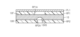
- the second through hole RP2A penetrates the second resist pattern RP2 along the thickness direction of the second resist pattern RP2.
- the second through hole RP2A is located within the first through hole RP1A.
- the metal mask substrate 10 may be wet-etched using, for example, a ferric chloride solution having a specific gravity of 47° Baume or more and 52° Baume or less.
- a ferric chloride solution having a specific gravity of 47° Baume or more and 52° Baume or less In the manufacturing method for the metal mask substrate 10 disclosed herein, even if a ferric chloride solution containing chloride ions that cause pitting corrosion is used as the etching solution, the occurrence of pitting corrosion is suppressed when forming through holes in the metal mask substrate 10.
- the contact angle of the resist patterns RP1, RP2 is preferably 40° or less, and more preferably 30° or less.
- a contact angle of 40° or less allows the etching liquid to easily penetrate into the through holes RP1A, RP2A of the resist patterns RP1, RP2.
- the contact angle in this disclosure is an angle measured by the ⁇ /2 method.
- the ⁇ /2 method is a contact angle measurement method that conforms to "6. Sessile drop method" in JIS R 3257:1999 "Test method for wettability of substrate glass surfaces.”
- the metal mask substrate 10 is etched from the surface 10F using the first resist pattern RP1.
- an etching solution containing, for example, chloride ions is used, as in the case of forming the small hole portion 10HS.
- the etching solution containing chloride ions may be, for example, a ferric chloride solution having a specific gravity of 47° Baume or more and 52° Baume or less.
- the large hole portion 10HL is formed so as to reach a portion of the second protective layer PL2 filled in the small hole portion 10HS, thereby connecting the large hole portion 10HL to the small hole portion 10HS.
- the first resist pattern RP1 is removed from the front surface 10F of the metal mask substrate 10, and the second protective layer PL2 is removed from the back surface 10R.
- a metal mask 20 having a through hole 20H.
- the large hole portion 20HL corresponds to the large hole portion 10HL formed in the metal mask substrate 10
- the small hole portion 20HS corresponds to the small hole portion 10HS formed in the metal mask substrate 10.
- the front surface 20F of the metal mask 20 corresponds to the front surface 10F of the metal mask substrate 10
- the back surface 20R of the metal mask 20 corresponds to the back surface 10R of the metal mask substrate 10.
- the second protective layer PL2 When the second protective layer PL2 is formed on the rear surface 10R of the metal mask substrate 10, the second resist pattern RP2 does not have to be removed from the rear surface 10R of the metal mask substrate 10. In this case, the second protective layer PL2 is formed on the second resist pattern RP2. The second protective layer PL2 is formed so that a portion of the second protective layer PL2 fills the small hole portion 10HS and also fills the second through hole RP2A of the second resist pattern RP2. After the large hole portion 10HL is formed in the metal mask substrate 10, the second resist pattern RP2 and the second protective layer PL2 are removed from the metal mask substrate 10.
- Example 1 An example and a comparative example will be described with reference to FIG. 18 to FIG. [Example 1]
- a metal plate was formed by rolling an ingot of an iron-nickel alloy to which additive elements including magnesium, aluminum, silicon, chromium, manganese, molybdenum, and cobalt were added. The metal plate was then annealed and then cut to obtain a metal plate having a desired length in the width direction of the metal plate. In this way, a metal mask substrate of Example 1 having a thickness of 25 ⁇ m was obtained.
- composition Analysis The metal mask substrates of each of the examples and comparative examples were subjected to composition analysis by X-ray fluorescence analysis (XRF) using an X-ray fluorescence composition analyzer (ZSX Primus IV, Rigaku Corporation).
- a dry film resist having a thickness of 10 ⁇ m was attached to the surface of the metal mask substrate of each example and each comparative example.
- a plurality of square openings each having a side length of 25 ⁇ m were formed in the dry film resist using a photolithography method, thereby obtaining a resist pattern.
- the area of the openings formed in the metal mask substrate was about 10% larger than the area of the openings formed in the dry film resist.
- a dry film resist having a contact angle of 77° with respect to the ferric chloride solution was used.
- the distance between the openings in the first direction was set to 25 ⁇ m
- the pitch of the openings in the second direction perpendicular to the first direction was set to 25 ⁇ m.
- the metal mask substrate on which the resist pattern was formed was wet-etched using ferric chloride solution so that the depth of the recesses formed by etching was 8 ⁇ m.
- the metal mask substrate was wet-etched under the following two conditions:
- a laser microscope (VK-X3000, Keyence Corporation) was used to capture images of the surface of each metal mask substrate. From the images of each metal mask substrate, the area of the openings located on the surface for 1,000 recesses was calculated by image analysis. A first average value for the area of all openings was calculated, and the sum of the areas of the openings from the smallest to the tenth smallest was calculated, excluding recesses with an area 30% or more smaller than the first average value. Next, a second average value was calculated, which is the average value for the area of each opening based on the sum. The calculated second average value was then set as the normal value for the area of the openings.
- the length of one side of the opening was changed to 20 ⁇ m while maintaining the same pitch of the openings as when the length of one side of the openings was 25 ⁇ m. Otherwise, six test pieces with different contact angles of the resist pattern were created using the same method as described above. In addition, the length of one side of the opening was changed to 30 ⁇ m while maintaining the same pitch of the openings as when the length of one side of the openings was 25 ⁇ m. Otherwise, six test pieces with different contact angles of the resist pattern were created using the same method as described above.
- the manganese element content be within the range of 0.247 mass% or more and 0.354 mass% or less. Also, from the viewpoint of suppressing the occurrence rate of recess expansion, it is more preferable that the manganese element content be within the range of 0.255 mass% or more and 0.354 mass% or less, and it is even more preferable that the manganese element content be within the range of 0.306 mass% or more and 0.354 mass% or less.
- the silicon element content be within the range of 0.026 mass % or more and 0.047 mass % or less.
- the manganese element content be within the range of 0.247 mass% or more and 0.354 mass% or less. Also, from the viewpoint of suppressing the occurrence rate of recess expansion, it is more preferable that the manganese element content be within the range of 0.259 mass% or more and 0.354 mass% or less.
- the silicon element content be within the range of 0.026 mass % or more and 0.047 mass % or less.
- Figures 21 and 22 are graphs obtained by multiple regression analysis of the relationship between the content of each added element and the incidence of recess expansion under condition 1.
- Figure 21 is a graph showing the relationship between the content of manganese element and the incidence of recess expansion.
- Figure 22 is a graph showing the relationship between the content of manganese element and the incidence of silicon expansion. Note that for Example 1, the incidence of recess expansion was set to 0.05% for the convenience of the regression analysis.
- the relationship between the depth of the recess and the incidence rate of recess expansion was as shown in FIG. 23, it was found that the incidence rate was 53% when the recess depth was 0.9 ⁇ m, 56% when the recess depth was 1.8 ⁇ m, and 49% when the depth was 3.4 ⁇ m. It was found that the incidence rate was 49% when the recess depth was 5.4 ⁇ m, and 50% when the recess depth was 8.0 ⁇ m. Thus, it was found that the recess expansion almost occurred by the time the recess depth reached 0.9 ⁇ m, and the incidence rate of recess expansion was maintained by the time the recess depth reached 8.0 ⁇ m.
- Figures 24 and 25 are SEM images of recesses formed on the surface of the first test piece.
- Figure 24 is an SEM image of a recess with a roughly uniform depth of 0.9 ⁇ m.
- Figure 25 is an SEM image of a recess formed by excessive etching in a portion of the area exposed through a through hole in the resist pattern.
- the expansion of the recess is caused by localized excessive etching in the early stages of wet etching. Furthermore, because localized and excessive etching occurs in the early stages of wet etching, it can be said that such etching is caused by pitting corrosion that occurs when the etching solution breaks through the oxide layer located on the surface of the metal mask substrate and comes into contact with the main layer.
- the metal mask substrate 10 contains 0.25 mass % or more of manganese, which has a lower standard electrode potential than iron and nickel. Therefore, the metal mask substrate 10 is in a state where it is easily corroded, and the corrosion potential generated when the etching solution ES contacts the metal mask substrate 10 is low, so that pitting corrosion is less likely to occur when the metal mask substrate 10 comes into contact with the etching solution ES. As a result, excessive wet etching is prevented from progressing locally in the metal mask substrate 10, and some of the through holes 20H among the multiple through holes 20H are prevented from becoming large.
- Metal mask substrate 10F Surface 10R: Back surface 10A: Main layer 10B1: First surface layer 10B2: Second surface layer 20: Metal mask 20F: Surface 20H: Through hole 20R: Back surface
Landscapes
- Chemical & Material Sciences (AREA)
- Engineering & Computer Science (AREA)
- Mechanical Engineering (AREA)
- Organic Chemistry (AREA)
- Metallurgy (AREA)
- Materials Engineering (AREA)
- Chemical Kinetics & Catalysis (AREA)
- Manufacturing & Machinery (AREA)
- Optics & Photonics (AREA)
- Physics & Mathematics (AREA)
- Electrodes For Cathode-Ray Tubes (AREA)
- Physical Vapour Deposition (AREA)
- Electroluminescent Light Sources (AREA)
- ing And Chemical Polishing (AREA)
Priority Applications (3)
| Application Number | Priority Date | Filing Date | Title |
|---|---|---|---|
| CN202380084854.XA CN120380191A (zh) | 2022-12-28 | 2023-12-19 | 金属掩模用基材、金属掩模、以及金属掩模的制造方法 |
| KR1020257023804A KR20250129698A (ko) | 2022-12-28 | 2023-12-19 | 메탈 마스크용 기재, 메탈 마스크 및 메탈 마스크의 제조 방법 |
| JP2024567650A JPWO2024143061A1 (https=) | 2022-12-28 | 2023-12-19 |
Applications Claiming Priority (2)
| Application Number | Priority Date | Filing Date | Title |
|---|---|---|---|
| JP2022212160 | 2022-12-28 | ||
| JP2022-212160 | 2022-12-28 |
Publications (1)
| Publication Number | Publication Date |
|---|---|
| WO2024143061A1 true WO2024143061A1 (ja) | 2024-07-04 |
Family
ID=91717450
Family Applications (1)
| Application Number | Title | Priority Date | Filing Date |
|---|---|---|---|
| PCT/JP2023/045440 Ceased WO2024143061A1 (ja) | 2022-12-28 | 2023-12-19 | メタルマスク用基材、メタルマスク、および、メタルマスクの製造方法 |
Country Status (4)
| Country | Link |
|---|---|
| JP (1) | JPWO2024143061A1 (https=) |
| KR (1) | KR20250129698A (https=) |
| CN (1) | CN120380191A (https=) |
| WO (1) | WO2024143061A1 (https=) |
Citations (2)
| Publication number | Priority date | Publication date | Assignee | Title |
|---|---|---|---|---|
| WO2020067537A1 (ja) * | 2018-09-27 | 2020-04-02 | 日鉄ケミカル&マテリアル株式会社 | メタルマスク材料及びその製造方法とメタルマスク |
| WO2022244701A1 (ja) * | 2021-05-17 | 2022-11-24 | 日鉄ケミカル&マテリアル株式会社 | 鉄系合金箔及びその製造方法、並びにそれを用いた部品 |
Family Cites Families (1)
| Publication number | Priority date | Publication date | Assignee | Title |
|---|---|---|---|---|
| WO2018235862A1 (ja) | 2017-06-20 | 2018-12-27 | 日立金属株式会社 | メタルマスク用薄板の製造方法及びメタルマスク用薄板 |
-
2023
- 2023-12-19 JP JP2024567650A patent/JPWO2024143061A1/ja active Pending
- 2023-12-19 WO PCT/JP2023/045440 patent/WO2024143061A1/ja not_active Ceased
- 2023-12-19 CN CN202380084854.XA patent/CN120380191A/zh active Pending
- 2023-12-19 KR KR1020257023804A patent/KR20250129698A/ko active Pending
Patent Citations (2)
| Publication number | Priority date | Publication date | Assignee | Title |
|---|---|---|---|---|
| WO2020067537A1 (ja) * | 2018-09-27 | 2020-04-02 | 日鉄ケミカル&マテリアル株式会社 | メタルマスク材料及びその製造方法とメタルマスク |
| WO2022244701A1 (ja) * | 2021-05-17 | 2022-11-24 | 日鉄ケミカル&マテリアル株式会社 | 鉄系合金箔及びその製造方法、並びにそれを用いた部品 |
Non-Patent Citations (1)
| Title |
|---|
| UEDA RYUJI: "Chemical Machining by Ferric Chloride Etchant", BOSHOKU GIJUTSU, XX, JP, vol. 38, no. 4, 1 January 1989 (1989-01-01), JP , pages 231 - 237, XP093187490, ISSN: 0010-9355, DOI: 10.3323/jcorr1974.38.4_231 * |
Also Published As
| Publication number | Publication date |
|---|---|
| CN120380191A (zh) | 2025-07-25 |
| KR20250129698A (ko) | 2025-08-29 |
| JPWO2024143061A1 (https=) | 2024-07-04 |
Similar Documents
| Publication | Publication Date | Title |
|---|---|---|
| JP7646790B2 (ja) | 蒸着マスク用金属板、蒸着マスク及びその製造方法 | |
| JP7476535B2 (ja) | 蒸着マスク、蒸着マスクの製造方法、および、表示装置の製造方法 | |
| JP5850185B2 (ja) | 対カーボン接触導電性と耐久性に優れた燃料電池セパレータ用チタン材又はチタン合金材、これを用いた燃料電池セパレータ、及び、燃料電池 | |
| TW202031913A (zh) | 金屬遮罩材料及其製造方法與金屬遮罩 | |
| CN1109121C (zh) | 超薄不锈钢箔 | |
| JP5850184B2 (ja) | 対カーボン接触導電性と耐久性に優れた燃料電池セパレータ用チタン又はチタン合金、これを用いた燃料電池セパレータ、及び、燃料電池 | |
| WO2024143061A1 (ja) | メタルマスク用基材、メタルマスク、および、メタルマスクの製造方法 | |
| US6559583B1 (en) | Shadow mask | |
| KR100486326B1 (ko) | 프레스 성형형 플랫 마스크용 Fe-Ni계 또는 Fe-Ni-Co계 합금 박대 | |
| KR20250166307A (ko) | 메탈 마스크용 기재, 메탈 마스크용 기재의 제조 방법, 및 메탈 마스크의 제조 방법 | |
| JP3545684B2 (ja) | エッチング穿孔性に優れたFe−Ni系合金シャドウマスク用素材 | |
| JPH09143625A (ja) | シャドウマスク用Fe−Ni系合金素材 | |
| KR100500490B1 (ko) | 섀도우마스크용 철-니켈계 및 철-니켈-코발트계 합금 스트립 | |
| JP2004043930A (ja) | シャドウマスク用Fe−Ni系合金素材及びその製造方法 | |
| US20250078690A1 (en) | Substrate for display | |
| KR100519615B1 (ko) | 저열팽창 합금박판 및 이를 이용한 새도우 마스크 | |
| JP2005281836A (ja) | エッチング性に優れたシャドウマスク用Fe−Ni系合金薄板 | |
| WO2025009388A1 (ja) | メタルマスク用基材、メタルマスク、メタルマスク用基材の製造方法、メタルマスクの製造方法、および、表示装置の製造方法 | |
| KR100486325B1 (ko) | 에칭 천공성이 우수한 플랫 마스크용 고강도 합금재 | |
| JPH1150200A (ja) | エッチング性に優れた電子部品用低熱膨張合金薄板 | |
| JP2001210232A (ja) | シャドウマスクの製造方法 | |
| JP2003082440A (ja) | 製造性およびエッチング性に優れた低熱膨張合金薄板 | |
| JPH1150146A (ja) | エッチング性に優れた電子部品用低熱膨張合金の製造方法 | |
| JP2002294407A (ja) | シャドウマスク材用表面高清浄度材 | |
| JPH1150201A (ja) | エッチング性に優れた電子部品用低熱膨張合金薄板 |
Legal Events
| Date | Code | Title | Description |
|---|---|---|---|
| 121 | Ep: the epo has been informed by wipo that ep was designated in this application |
Ref document number: 23911841 Country of ref document: EP Kind code of ref document: A1 |
|
| WWE | Wipo information: entry into national phase |
Ref document number: 2024567650 Country of ref document: JP |
|
| WWE | Wipo information: entry into national phase |
Ref document number: 202380084854.X Country of ref document: CN |
|
| ENP | Entry into the national phase |
Ref document number: 1020257023804 Country of ref document: KR Free format text: ST27 STATUS EVENT CODE: A-0-1-A10-A15-NAP-PA0105 (AS PROVIDED BY THE NATIONAL OFFICE) |
|
| WWE | Wipo information: entry into national phase |
Ref document number: 1020257023804 Country of ref document: KR |
|
| WWP | Wipo information: published in national office |
Ref document number: 202380084854.X Country of ref document: CN |
|
| NENP | Non-entry into the national phase |
Ref country code: DE |
|
| WWP | Wipo information: published in national office |
Ref document number: 1020257023804 Country of ref document: KR |
|
| 122 | Ep: pct application non-entry in european phase |
Ref document number: 23911841 Country of ref document: EP Kind code of ref document: A1 |