WO2024134864A1 - 光モジュール - Google Patents
光モジュール Download PDFInfo
- Publication number
- WO2024134864A1 WO2024134864A1 PCT/JP2022/047584 JP2022047584W WO2024134864A1 WO 2024134864 A1 WO2024134864 A1 WO 2024134864A1 JP 2022047584 W JP2022047584 W JP 2022047584W WO 2024134864 A1 WO2024134864 A1 WO 2024134864A1
- Authority
- WO
- WIPO (PCT)
- Prior art keywords
- optical
- section
- capacitor
- stem
- submount
- Prior art date
- Legal status (The legal status is an assumption and is not a legal conclusion. Google has not performed a legal analysis and makes no representation as to the accuracy of the status listed.)
- Ceased
Links
Images


Classifications
-
- G—PHYSICS
- G02—OPTICS
- G02F—OPTICAL DEVICES OR ARRANGEMENTS FOR THE CONTROL OF LIGHT BY MODIFICATION OF THE OPTICAL PROPERTIES OF THE MEDIA OF THE ELEMENTS INVOLVED THEREIN; NON-LINEAR OPTICS; FREQUENCY-CHANGING OF LIGHT; OPTICAL LOGIC ELEMENTS; OPTICAL ANALOGUE/DIGITAL CONVERTERS
- G02F1/00—Devices or arrangements for the control of the intensity, colour, phase, polarisation or direction of light arriving from an independent light source, e.g. switching, gating or modulating; Non-linear optics
- G02F1/01—Devices or arrangements for the control of the intensity, colour, phase, polarisation or direction of light arriving from an independent light source, e.g. switching, gating or modulating; Non-linear optics for the control of the intensity, phase, polarisation or colour
- G02F1/015—Devices or arrangements for the control of the intensity, colour, phase, polarisation or direction of light arriving from an independent light source, e.g. switching, gating or modulating; Non-linear optics for the control of the intensity, phase, polarisation or colour based on semiconductor elements having potential barriers, e.g. having a PN or PIN junction
-
- H—ELECTRICITY
- H01—ELECTRIC ELEMENTS
- H01S—DEVICES USING THE PROCESS OF LIGHT AMPLIFICATION BY STIMULATED EMISSION OF RADIATION [LASER] TO AMPLIFY OR GENERATE LIGHT; DEVICES USING STIMULATED EMISSION OF ELECTROMAGNETIC RADIATION IN WAVE RANGES OTHER THAN OPTICAL
- H01S5/00—Semiconductor lasers
- H01S5/02—Structural details or components not essential to laser action
- H01S5/022—Mountings; Housings
- H01S5/02208—Mountings; Housings characterised by the shape of the housings
- H01S5/02212—Can-type, e.g. TO-CAN housings with emission along or parallel to symmetry axis
-
- H—ELECTRICITY
- H01—ELECTRIC ELEMENTS
- H01S—DEVICES USING THE PROCESS OF LIGHT AMPLIFICATION BY STIMULATED EMISSION OF RADIATION [LASER] TO AMPLIFY OR GENERATE LIGHT; DEVICES USING STIMULATED EMISSION OF ELECTROMAGNETIC RADIATION IN WAVE RANGES OTHER THAN OPTICAL
- H01S5/00—Semiconductor lasers
- H01S5/02—Structural details or components not essential to laser action
- H01S5/022—Mountings; Housings
- H01S5/0233—Mounting configuration of laser chips
-
- H—ELECTRICITY
- H01—ELECTRIC ELEMENTS
- H01S—DEVICES USING THE PROCESS OF LIGHT AMPLIFICATION BY STIMULATED EMISSION OF RADIATION [LASER] TO AMPLIFY OR GENERATE LIGHT; DEVICES USING STIMULATED EMISSION OF ELECTROMAGNETIC RADIATION IN WAVE RANGES OTHER THAN OPTICAL
- H01S5/00—Semiconductor lasers
- H01S5/02—Structural details or components not essential to laser action
- H01S5/024—Arrangements for thermal management
-
- H—ELECTRICITY
- H01—ELECTRIC ELEMENTS
- H01S—DEVICES USING THE PROCESS OF LIGHT AMPLIFICATION BY STIMULATED EMISSION OF RADIATION [LASER] TO AMPLIFY OR GENERATE LIGHT; DEVICES USING STIMULATED EMISSION OF ELECTROMAGNETIC RADIATION IN WAVE RANGES OTHER THAN OPTICAL
- H01S5/00—Semiconductor lasers
- H01S5/02—Structural details or components not essential to laser action
- H01S5/026—Monolithically integrated components, e.g. waveguides, monitoring photo-detectors, drivers
-
- H—ELECTRICITY
- H01—ELECTRIC ELEMENTS
- H01S—DEVICES USING THE PROCESS OF LIGHT AMPLIFICATION BY STIMULATED EMISSION OF RADIATION [LASER] TO AMPLIFY OR GENERATE LIGHT; DEVICES USING STIMULATED EMISSION OF ELECTROMAGNETIC RADIATION IN WAVE RANGES OTHER THAN OPTICAL
- H01S5/00—Semiconductor lasers
- H01S5/04—Processes or apparatus for excitation, e.g. pumping, e.g. by electron beams
- H01S5/042—Electrical excitation ; Circuits therefor
Definitions
- This disclosure relates to an optical module.
- a semiconductor optical integrated device that monolithically integrates a semiconductor laser section, an optical modulator section, and an optical amplifier section is used as a light source for long-distance optical communications such as optical fiber communications (Patent Document 1).
- the optical modulator section is a type of external modulator, and since there is less degradation in the signal waveform compared to the direct modulation method that directly modulates the laser light intensity, high-speed and long-distance optical fiber transmission is possible.
- the optical amplifier section functions to amplify the modulated light.
- the capacitor for the semiconductor laser section and the capacitor for the optical amplifier section are shared, and only one capacitor is provided.
- the semiconductor optical integrated element is mounted at an angle to the direction perpendicular to the surface of the stem.
- the semiconductor laser section and the optical amplifier section are electrically connected in parallel, so the same current flows through the semiconductor laser section and the optical amplifier section, which creates a practical problem in that it is difficult to control the two sections independently.
- This disclosure has been made to resolve the above-mentioned problems, and aims to provide an optical module that has high current controllability and can be miniaturized.
- the optical module comprises: a base portion disposed on a surface side of the stem, the base portion having a bottom surface facing the surface of the stem and a side surface perpendicular to the surface of the stem; A submount disposed on a side surface of the base; a semiconductor optical integrated device mounted on the submount and including, from a bottom surface side of a base, a semiconductor laser section, an optical modulator section, and an optical amplifier section, each of which is electrically independent from the other; a capacitor for a semiconductor laser portion connected to a semiconductor laser portion of the semiconductor optical integrated device; an optical modulator capacitor connected to an optical modulator of the semiconductor optical integrated device; a capacitor for an optical amplifier section connected to an optical amplifier section of the semiconductor optical integrated device; Equipped with.
- the optical module disclosed herein allows current to flow independently through capacitors that are electrically connected to the semiconductor laser section, optical modulator section, and optical amplifier section of the semiconductor optical integrated device mounted thereon, resulting in an optical module that has high current controllability and can be made compact.
- FIG. 11 is a schematic view of an optical module according to a second embodiment.
- FIG. 11 is a side view of an optical module according to a second embodiment.
- FIG. 11 is a side view of an optical module according to a second embodiment.
- FIG. 11 is a side view of an optical module according to a second embodiment.
- FIG. 11 is a schematic view of an optical module according to a third embodiment.
- FIG. 11 is a side view of an optical module according to a third embodiment.
- FIG. 11 is a side view of an optical module according to a third embodiment.
- FIG. 13 is a schematic view of an optical module according to a fourth embodiment.
- FIG. 13 is a side view of an optical module according to a fourth embodiment.
- FIG. 13 is a side view of an optical module according to a fourth embodiment.
- FIG. 13 is a schematic view of an optical module according to a fifth embodiment.
- FIG. 13 is a side view of an optical module according to a fifth embodiment.
- FIG. 13 is a side view of an optical module according to a fifth embodiment.
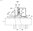
- FIG. 1 is a schematic view of an optical module 100 according to the first embodiment.
- Fig. 2 and Fig. 3 are side views of the optical module 100 according to the first embodiment.
- the stem 1 is generally circular and plate-like.
- the surface of the stem 1 is made of a material with high thermal conductivity, such as copper (Cu), and is plated with Au.
- the stem 1 has multiple lead pins 2a to 2f that penetrate the stem 1.
- Glass 3 is generally used to secure lead pins 2a to 2f to stem 1. If impedance mismatch occurs, multiple reflections of the signal will cause degradation of the frequency response characteristics, making high-speed modulation difficult. Therefore, glass 3 is made of a material with a low dielectric constant.
- the temperature control module 10 is disposed on the surface 1a of the stem.
- the surface 1a of the stem refers to the flat surface of the stem 1, which is in the shape of a circular plate, from which the lead pins 2a to 2f protrude.
- the temperature control module 10 is configured to sandwich a plurality of thermoelectric elements made of a material such as bismuth telluride (BiTe) between a lower substrate and an upper substrate made of a material such as aluminum nitride (AlN).
- the lower substrate of the temperature control module 10 has a protruding portion that protrudes in a direction parallel to the surface 1a of the stem more than the upper substrate, and electrode patterns 10a and 10b for supplying power to the thermoelectric elements (not shown) are provided on this protruding portion.
- the temperature control module 10 is provided to control the temperature of the semiconductor optical integrated element 50, which will be described later. In the optical module 100 according to the first embodiment, the temperature control module 10 may be omitted.
- a pedestal portion 20 is installed on the surface of the temperature control module 10.
- the bottom surface portion 20a of the pedestal portion faces the surface 1a of the stem via the temperature control module 10.
- the bottom surface portion 20a of the pedestal portion and the surface of the temperature control module 10 are joined by a joining material such as SnAgCu solder or AuSn solder.
- the base 20 has side portions 20b and 20c.
- the base 20 is made of a block of metal material, for example, Cu or other material with high thermal conductivity, with Au plating applied to the surface.
- the base 20, which is a separate part from the stem 1, may be mounted on the stem 1, or the stem 1 and the base 20 may be molded as a single unit.
- the submount 30 is mounted on the side portion 20b of the base.
- the submount 30 is, for example, a rectangular parallelepiped plate-like member made of a dielectric material.
- the submount 30 is made of a ceramic material such as AlN, and has electrical insulation and heat transfer functions.
- the submount 30 has a main surface and a back surface opposite each other, and four side surfaces.
- the back surface of the submount 30 is mounted on the side portion 20b of the base.
- a metal pattern is patterned on the main surface of the submount 30.
- a semiconductor optical integrated element 50 is mounted on the main surface side of the submount 30.
- the semiconductor optical integrated element 50 is composed of a semiconductor laser section 50a, an optical modulator section 50b, and an optical amplifier section 50c.
- the sections are arranged from the bottom surface 20a side of the base in the order of the semiconductor laser section 50a, the optical modulator section 50b, and the optical amplifier section 50c.
- the semiconductor laser section 50a, the optical modulator section 50b, and the optical amplifier section 50c are each electrically independent.
- the semiconductor optical integrated element 50 is mounted at an angle to the direction perpendicular to the surface 1a of the stem.
- the semiconductor laser section 50a of the semiconductor optical integrated device 50 is, for example, a distributed feedback semiconductor laser (DFB laser).
- the optical modulator section 50b of the semiconductor optical integrated device 50 is, for example, an electroabsorption optical modulator using an InGaAsP-based quantum well absorption layer.
- the optical amplifier section 50c of the semiconductor optical integrated device 50 is, for example, an InGaAsP-based optical amplifier.
- the oscillation wavelength of the semiconductor optical integrated element 50 varies with changes in temperature, so it is necessary to keep the temperature of the semiconductor optical integrated element 50 as constant as possible.
- the temperature control module 10 cools it, while when the temperature of the semiconductor optical integrated element 50 drops, the temperature control module 10 generates heat, thereby keeping the temperature of the semiconductor optical integrated element 50 constant.
- Heat generated by the operation of the semiconductor optical integrated element 50 is transferred to the upper substrate of the temperature control module 10 via the submount 30.
- the temperature control module 10 absorbs the heat generated by the semiconductor optical integrated element 50.
- the heat absorbed by the temperature control module 10 is dissipated from the lower substrate of the temperature control module 10 through the stem 1 to a heat sink (not shown) on the back side of the stem 1.
- a capacitor 60 for the semiconductor laser section, a capacitor 61 for the optical modulator section, and a capacitor 62 for the optical amplifier section are arranged in this order on the side surface 20b of the base along the side perpendicular to the surface 1a of the stem of the submount 30 mounted on the side surface 20b of the base from the bottom surface 20a side of the base.
- Thermistor 55 is installed on side surface 20c of the pedestal opposite side surface 20b of the pedestal on which submount 30 is installed.
- the thermistor 55 is a type of temperature sensor, and indirectly measures the temperature of semiconductor optical integrated device 50.
- the temperature measured by the thermistor 55 is fed back to temperature control module 10.
- temperature control module 10 controls the temperature of semiconductor optical integrated device 50, thereby stabilizing the temperature of semiconductor optical integrated device 50. As a result, a constant oscillation wavelength is stably obtained.
- the lead pin 2a is electrically connected to the thermistor 55 via a conductive wire W1.
- the lead pin 2b is electrically connected to the semiconductor laser capacitor 60 via a conductive wire W2.
- the lead pin 2c is electrically connected to the optical amplifier capacitor 62 via a conductive wire W3.
- the lead pin 2d is electrically connected to the electrode pattern 10a of the temperature control module 10 via a conductive wire W4.
- the lead pin 2e is electrically connected to the electrode pattern 10b of the temperature control module 10 via a conductive wire W5.
- the lead pin 2f is electrically connected to the electrode pattern 80a of the auxiliary substrate 80 fixed to the side of the auxiliary block 79, and is electrically connected to the optical modulator section 50b of the semiconductor optical integrated device 50 via the electrode pattern 30e on the submount 30.
- the arrangement of the conductive wires and electrode patterns in FIG. 2 and FIG. 3 is the same as that in FIG. 1, the symbols of the conductive wires and electrode patterns are omitted to avoid complication.
- the semiconductor laser capacitor 60 is first electrically connected to the electrode pattern 30a on the submount 30 via a conductive wire W6, and is then electrically connected to the semiconductor laser section 50a of the semiconductor optical integrated device 50 via a conductive wire W7.
- the optical modulator capacitor 61 is first electrically connected to the electrode pattern 30b on the submount 30 via conductive wire W8, and is then electrically connected to the optical modulator 50b of the semiconductor optical integrated device 50 via conductive wire W9.
- the optical amplifier capacitor 62 is first electrically connected to the electrode pattern 30c on the submount 30 via conductive wire W10, and is then electrically connected to the optical amplifier section 50c of the semiconductor optical integrated device 50 via conductive wire W11.
- the electrode pattern 80a of the auxiliary substrate 80 is electrically connected to the electrode pattern 30e on the submount 30 via a conductive wire W23.
- the electrode pattern 80b of the auxiliary substrate 80 is electrically connected to the electrode pattern 30d on the submount 30 via a conductive wire W21.
- the electrode pattern 80c of the auxiliary substrate 80 is electrically connected to the electrode pattern 30f on the submount 30 via a conductive wire W22.
- the optical module 100 uses a CAN package 90 as shown in FIG. 5 as a package. That is, the temperature control module 10, the base 20, the submount 30, the auxiliary block 79, the auxiliary substrate 80, etc., which are provided on the front surface 1a side of the stem, are housed inside the CAN case 91. Note that the lead pins 2 protrude from the rear surface side of the stem 1.
- the optical module 100 according to the first embodiment employs the above-mentioned configuration, so that the current of each of the semiconductor laser section 50a, the optical modulator section 50b, and the optical amplifier section 50c can be individually controlled via the capacitor 60 for the semiconductor laser section, the capacitor 61 for the optical modulator section, and the capacitor 62 for the optical amplifier section, respectively, and therefore the controllability of the drive current for the semiconductor optical integrated device 50 is high. In other words, the effect is achieved of improving the current controllability of the optical module 100 according to the first embodiment.
- the capacitor 60 for the semiconductor laser section, the capacitor 61 for the optical modulator section, and the capacitor 62 for the optical amplifier section are arranged in this order on the side surface 20b of the base along the side surface perpendicular to the surface 1a of the stem of the submount 30 mounted on the side surface 20b of the base from the bottom surface 20a side of the base, which has the effect of making it possible to miniaturize the optical module.
- FIG. 6 is a schematic view of an optical module 110 according to the second embodiment.
- Figs. 7 and 8 are side views of the optical module 110 according to the second embodiment. The following description focuses on the differences from the optical module 100 according to the first embodiment.
- the arrangement of the conductive wires and electrode patterns is the same as in the first embodiment, and therefore the reference numerals are omitted to avoid complication.
- the capacitor 61 for the optical modulator section is disposed on the submount 30.
- the capacitor 60 for the semiconductor laser section and the capacitor 62 for the optical amplifier section are each disposed on the surface of the upper substrate of the temperature control module 10.
- the capacitors By arranging the capacitors as described above, it is possible to reduce the width along the side surface 20b of the base compared to the structure of the optical module 100 according to the first embodiment.
- the CAN package 90 that houses the stem 1, temperature control module 10, base 20, submount 30, auxiliary block 79, auxiliary substrate 80, etc. of the optical module 110 can be made smaller.
- the temperature control module 10 may have the same area as the bottom surface 20a of the base, and the capacitor 60 for the semiconductor laser section and the capacitor 62 for the optical amplifier section may be placed directly on the surface 1a of the stem.
- FIG. 9 is a schematic view of an optical module 120 according to the third embodiment.
- Figs. 10 and 11 are side views of the optical module 120 according to the third embodiment. The following description will focus on the differences from the optical module 100 according to the first embodiment.
- the arrangement of the conductive wires and electrode patterns is the same as in the first embodiment, and therefore, in order to avoid complication, reference numerals other than those for parts necessary for the description are omitted.
- the base 20 has a rectangular parallelepiped shape.
- parts of the electrode pattern 30a and the electrode pattern 30c on the submount 30 are also provided on the side portions of the submount 30.
- the capacitor 61 for the optical modulator section is disposed on the submount 30.
- the capacitor 60 for the semiconductor laser section and the capacitor 62 for the optical amplifier section are disposed on the side section 20d of the pedestal section.
- the side section 20d of the pedestal section refers to the side section that is closer to the capacitor 61 for the optical modulator section out of the two side sections perpendicular to the side sections 20b and 20c of the pedestal section that face each other.
- the capacitor 61 for the optical modulator section is placed on the submount 30, and the capacitor 60 for the semiconductor laser section and the capacitor 62 for the optical amplifier section are placed on the other side portion 20d of the base along the side portion 20b of the base on which the submount 30 is placed.
- the reason why a part of the electrode pattern 30a and the electrode pattern 30c are also provided on the side portion of the submount 30 is that such an arrangement is necessary in order to connect, with conductive wires, the capacitor 60 for the semiconductor laser section mounted on the side portion 20d of the pedestal and the electrode pattern 30a, and the capacitor 62 for the optical amplifier section and the electrode pattern 30c.
- the capacitors By arranging the capacitors as described above, it is possible to reduce the width along the side portion 20b of the base compared to the structure of the optical module 100 according to the first embodiment.
- the CAN package 90 that houses the stem 1, temperature control module 10, base portion 20, submount 30, auxiliary block 79, auxiliary substrate 80, etc. of the optical module 120 can be made smaller.
- small conductive blocks may be bonded onto the electrode pattern 30a and the electrode pattern 30c of the submount 30, respectively, and the conductive blocks may be connected to the capacitor 60 for the semiconductor laser section and the capacitor 62 for the optical amplifier section by conductive wires.
- FIG. 12 is a schematic view of an optical module 130 according to the fourth embodiment.
- Figs. 13 and 14 are side views of the optical module 130 according to the fourth embodiment. The following description focuses on the differences from the optical module 100 according to the first embodiment.
- the arrangement of the conductive wires and electrode patterns is the same as in the first embodiment, and therefore the reference numerals are omitted to avoid complication.
- the arrangement of the capacitors is the same as that of the optical module 100 according to the first embodiment.
- the optical module 130 according to the fourth embodiment is characterized in that the cross-sectional shape of the other side surface 20d of the base along the side surface 20b of the base on which the submount 30 is installed is L-shaped.
- the CAN package 90 that houses the stem 1, temperature control module 10, base portion 20, submount 30, auxiliary block 79, auxiliary substrate 80, etc. of the optical module 130 can be made smaller.
- FIG. 15 is a schematic view of an optical module 140 according to embodiment 4.
- Figs. 16 and 17 are side views of the optical module 140 according to embodiment 4.
- the arrangement of the conductive wires and electrode patterns is similar to that of embodiment 1, and therefore the reference numerals are omitted to avoid complication.
- the optical module 140 according to the fifth embodiment does not have a base 20, and instead the submount 30 also serves as a base.
- the arrangement of the capacitors is the same as that of the optical module 100 according to the first embodiment.
- the optical module 140 there is no need to provide a base portion 20 as in the first to fourth embodiments, so the number of parts in the optical module can be reduced.
- the height of the submount 30 is lower than the height of the base portion 20 in the first to fourth embodiments, the CAN package 90 that houses the stem 1, temperature control module 10, submount 30, auxiliary block 79, auxiliary substrate 80, etc. of the optical module 140 can be made smaller.
Landscapes
- Physics & Mathematics (AREA)
- General Physics & Mathematics (AREA)
- Optics & Photonics (AREA)
- Condensed Matter Physics & Semiconductors (AREA)
- Electromagnetism (AREA)
- Nonlinear Science (AREA)
- Semiconductor Lasers (AREA)
- Optical Modulation, Optical Deflection, Nonlinear Optics, Optical Demodulation, Optical Logic Elements (AREA)
Priority Applications (5)
| Application Number | Priority Date | Filing Date | Title |
|---|---|---|---|
| CN202280102059.4A CN120345142A (zh) | 2022-12-23 | 2022-12-23 | 光模块 |
| PCT/JP2022/047584 WO2024134864A1 (ja) | 2022-12-23 | 2022-12-23 | 光モジュール |
| JP2023525029A JP7466773B1 (ja) | 2022-12-23 | 2022-12-23 | 光モジュール |
| TW112148678A TWI870154B (zh) | 2022-12-23 | 2023-12-14 | 光模組 |
| JP2024005030A JP7734768B2 (ja) | 2022-12-23 | 2024-01-17 | 光モジュール |
Applications Claiming Priority (1)
| Application Number | Priority Date | Filing Date | Title |
|---|---|---|---|
| PCT/JP2022/047584 WO2024134864A1 (ja) | 2022-12-23 | 2022-12-23 | 光モジュール |
Publications (1)
| Publication Number | Publication Date |
|---|---|
| WO2024134864A1 true WO2024134864A1 (ja) | 2024-06-27 |
Family
ID=90622478
Family Applications (1)
| Application Number | Title | Priority Date | Filing Date |
|---|---|---|---|
| PCT/JP2022/047584 Ceased WO2024134864A1 (ja) | 2022-12-23 | 2022-12-23 | 光モジュール |
Country Status (4)
| Country | Link |
|---|---|
| JP (2) | JP7466773B1 (https=) |
| CN (1) | CN120345142A (https=) |
| TW (1) | TWI870154B (https=) |
| WO (1) | WO2024134864A1 (https=) |
Cited By (1)
| Publication number | Priority date | Publication date | Assignee | Title |
|---|---|---|---|---|
| JP7745811B1 (ja) * | 2024-12-20 | 2025-09-29 | 三菱電機株式会社 | Can型光モジュール |
Families Citing this family (1)
| Publication number | Priority date | Publication date | Assignee | Title |
|---|---|---|---|---|
| WO2025229704A1 (ja) * | 2024-04-30 | 2025-11-06 | 三菱電機株式会社 | 光モジュール |
Citations (11)
| Publication number | Priority date | Publication date | Assignee | Title |
|---|---|---|---|---|
| JPH09504939A (ja) * | 1995-01-17 | 1997-05-13 | エルディティ ゲーエムベーハー ウント シーオー.レーザー−ディスプレー−テクノロギー カーゲー | 増幅器 |
| US20030136972A1 (en) * | 2002-01-09 | 2003-07-24 | Bernhard Stegmuller | Optoelectronic module |
| JP2015088641A (ja) * | 2013-10-31 | 2015-05-07 | 三菱電機株式会社 | 光モジュール |
| JP2017049434A (ja) * | 2015-09-02 | 2017-03-09 | 日本電信電話株式会社 | 光トリガパルス発生器 |
| JP2019033116A (ja) * | 2017-08-04 | 2019-02-28 | 日本電信電話株式会社 | 半導体光集積素子 |
| JP2019057543A (ja) * | 2017-09-19 | 2019-04-11 | 日本電信電話株式会社 | 半導体光集積素子 |
| WO2019155602A1 (ja) * | 2018-02-09 | 2019-08-15 | 三菱電機株式会社 | 光モジュール |
| WO2021059447A1 (ja) * | 2019-09-26 | 2021-04-01 | 日本電信電話株式会社 | 光送信器 |
| WO2021210217A1 (ja) * | 2020-04-15 | 2021-10-21 | 株式会社村田製作所 | レーザダイオード駆動回路 |
| JP6984801B1 (ja) * | 2021-04-27 | 2021-12-22 | 三菱電機株式会社 | 半導体レーザ光源装置 |
| JP2022099537A (ja) * | 2020-12-23 | 2022-07-05 | CIG Photonics Japan株式会社 | 光モジュール |
Family Cites Families (11)
| Publication number | Priority date | Publication date | Assignee | Title |
|---|---|---|---|---|
| JPH04258107A (ja) * | 1991-02-13 | 1992-09-14 | Fujitsu Ltd | チップ型コンデンサの実装構造およびその実装方法 |
| JP2001209017A (ja) | 1999-11-15 | 2001-08-03 | Mitsubishi Electric Corp | 光電変換半導体装置 |
| JP4002231B2 (ja) * | 2003-11-12 | 2007-10-31 | 浜松ホトニクス株式会社 | 高周波信号伝送用光モジュール及びその製造方法 |
| JP5038746B2 (ja) | 2007-03-13 | 2012-10-03 | 富士通株式会社 | 光半導体素子の製造方法 |
| JP5823921B2 (ja) * | 2012-06-13 | 2015-11-25 | 日本電信電話株式会社 | 半導体光集積素子 |
| JPWO2016136183A1 (ja) * | 2015-02-23 | 2017-07-20 | 日本電信電話株式会社 | Soa集積ea−dfbレーザ及びその駆動方法 |
| JP6866976B2 (ja) | 2016-10-27 | 2021-04-28 | 住友電工デバイス・イノベーション株式会社 | 半導体レーザ装置の動作条件決定方法 |
| JP2019021866A (ja) * | 2017-07-21 | 2019-02-07 | 住友電工デバイス・イノベーション株式会社 | 半導体レーザ装置 |
| JP2019219537A (ja) * | 2018-06-20 | 2019-12-26 | ルネサスエレクトロニクス株式会社 | 半導体装置 |
| CN109417272B (zh) * | 2018-09-20 | 2020-10-09 | 索尔思光电(成都)有限公司 | 用于光发射器的抗阻匹配电路及其制造和使用方法 |
| JP7430569B2 (ja) | 2020-04-24 | 2024-02-13 | CIG Photonics Japan株式会社 | 光モジュール |
-
2022
- 2022-12-23 CN CN202280102059.4A patent/CN120345142A/zh active Pending
- 2022-12-23 WO PCT/JP2022/047584 patent/WO2024134864A1/ja not_active Ceased
- 2022-12-23 JP JP2023525029A patent/JP7466773B1/ja active Active
-
2023
- 2023-12-14 TW TW112148678A patent/TWI870154B/zh active
-
2024
- 2024-01-17 JP JP2024005030A patent/JP7734768B2/ja active Active
Patent Citations (11)
| Publication number | Priority date | Publication date | Assignee | Title |
|---|---|---|---|---|
| JPH09504939A (ja) * | 1995-01-17 | 1997-05-13 | エルディティ ゲーエムベーハー ウント シーオー.レーザー−ディスプレー−テクノロギー カーゲー | 増幅器 |
| US20030136972A1 (en) * | 2002-01-09 | 2003-07-24 | Bernhard Stegmuller | Optoelectronic module |
| JP2015088641A (ja) * | 2013-10-31 | 2015-05-07 | 三菱電機株式会社 | 光モジュール |
| JP2017049434A (ja) * | 2015-09-02 | 2017-03-09 | 日本電信電話株式会社 | 光トリガパルス発生器 |
| JP2019033116A (ja) * | 2017-08-04 | 2019-02-28 | 日本電信電話株式会社 | 半導体光集積素子 |
| JP2019057543A (ja) * | 2017-09-19 | 2019-04-11 | 日本電信電話株式会社 | 半導体光集積素子 |
| WO2019155602A1 (ja) * | 2018-02-09 | 2019-08-15 | 三菱電機株式会社 | 光モジュール |
| WO2021059447A1 (ja) * | 2019-09-26 | 2021-04-01 | 日本電信電話株式会社 | 光送信器 |
| WO2021210217A1 (ja) * | 2020-04-15 | 2021-10-21 | 株式会社村田製作所 | レーザダイオード駆動回路 |
| JP2022099537A (ja) * | 2020-12-23 | 2022-07-05 | CIG Photonics Japan株式会社 | 光モジュール |
| JP6984801B1 (ja) * | 2021-04-27 | 2021-12-22 | 三菱電機株式会社 | 半導体レーザ光源装置 |
Cited By (1)
| Publication number | Priority date | Publication date | Assignee | Title |
|---|---|---|---|---|
| JP7745811B1 (ja) * | 2024-12-20 | 2025-09-29 | 三菱電機株式会社 | Can型光モジュール |
Also Published As
| Publication number | Publication date |
|---|---|
| CN120345142A (zh) | 2025-07-18 |
| JP7466773B1 (ja) | 2024-04-12 |
| JP2024091613A (ja) | 2024-07-04 |
| JPWO2024134864A1 (https=) | 2024-06-27 |
| JP7734768B2 (ja) | 2025-09-05 |
| TWI870154B (zh) | 2025-01-11 |
| TW202427896A (zh) | 2024-07-01 |
Similar Documents
| Publication | Publication Date | Title |
|---|---|---|
| KR100575969B1 (ko) | 티오-캔 구조의 광 모듈 | |
| JP7734768B2 (ja) | 光モジュール | |
| JP5144628B2 (ja) | To−can型tosaモジュール | |
| CN107430293A (zh) | 高频传输线路以及光电路 | |
| US6404042B1 (en) | Subcarrier and semiconductor device | |
| JP2003198042A (ja) | 光モジュール、および光送信もしくは光受信装置 | |
| US6735353B2 (en) | Module for optical transmitter | |
| JP6984801B1 (ja) | 半導体レーザ光源装置 | |
| JP7020590B1 (ja) | レーザ光源装置 | |
| JP2002131712A (ja) | 光デバイスおよびその製造方法 | |
| JP2013110138A (ja) | 発光モジュール | |
| JP2006024623A (ja) | 光モジュール | |
| US20030193095A1 (en) | Optical module equipped with a wiring plate | |
| JP7019838B2 (ja) | 光モジュール | |
| JP4587218B2 (ja) | パッケージ型半導体装置 | |
| JP7544304B1 (ja) | 光モジュールおよび光トランシーバ | |
| JPH11186668A (ja) | 光半導体モジュール | |
| TWI863260B (zh) | 半導體雷射光源裝置 | |
| JP2022076388A (ja) | 光半導体モジュール | |
| JP2010123775A (ja) | 光送信モジュール用の熱電モジュールおよび光送信モジュール | |
| CN115087191A (zh) | 高带宽的eml基板 | |
| JP5837389B2 (ja) | 光通信装置 | |
| JP2007036046A (ja) | 光送信デバイス | |
| JP7246590B1 (ja) | 半導体レーザ光源装置 | |
| WO2026062918A1 (ja) | 光送信モジュール |
Legal Events
| Date | Code | Title | Description |
|---|---|---|---|
| WWE | Wipo information: entry into national phase |
Ref document number: 2023525029 Country of ref document: JP |
|
| 121 | Ep: the epo has been informed by wipo that ep was designated in this application |
Ref document number: 22969247 Country of ref document: EP Kind code of ref document: A1 |
|
| WWE | Wipo information: entry into national phase |
Ref document number: 202280102059.4 Country of ref document: CN |
|
| WWP | Wipo information: published in national office |
Ref document number: 202280102059.4 Country of ref document: CN |
|
| NENP | Non-entry into the national phase |
Ref country code: DE |
|
| 122 | Ep: pct application non-entry in european phase |
Ref document number: 22969247 Country of ref document: EP Kind code of ref document: A1 |