WO2024116873A1 - 半導体モジュール - Google Patents
半導体モジュール Download PDFInfo
- Publication number
- WO2024116873A1 WO2024116873A1 PCT/JP2023/041293 JP2023041293W WO2024116873A1 WO 2024116873 A1 WO2024116873 A1 WO 2024116873A1 JP 2023041293 W JP2023041293 W JP 2023041293W WO 2024116873 A1 WO2024116873 A1 WO 2024116873A1
- Authority
- WO
- WIPO (PCT)
- Prior art keywords
- layer
- heat dissipation
- dissipation member
- semiconductor module
- conductive layer
- Prior art date
- Legal status (The legal status is an assumption and is not a legal conclusion. Google has not performed a legal analysis and makes no representation as to the accuracy of the status listed.)
- Ceased
Links
Images


Classifications
-
- H—ELECTRICITY
- H10—SEMICONDUCTOR DEVICES; ELECTRIC SOLID-STATE DEVICES NOT OTHERWISE PROVIDED FOR
- H10W—GENERIC PACKAGES, INTERCONNECTIONS, CONNECTORS OR OTHER CONSTRUCTIONAL DETAILS OF DEVICES COVERED BY CLASS H10
- H10W40/00—Arrangements for thermal protection or thermal control
- H10W40/10—Arrangements for heating
-
- H—ELECTRICITY
- H10—SEMICONDUCTOR DEVICES; ELECTRIC SOLID-STATE DEVICES NOT OTHERWISE PROVIDED FOR
- H10W—GENERIC PACKAGES, INTERCONNECTIONS, CONNECTORS OR OTHER CONSTRUCTIONAL DETAILS OF DEVICES COVERED BY CLASS H10
- H10W40/00—Arrangements for thermal protection or thermal control
- H10W40/20—Arrangements for cooling
- H10W40/22—Arrangements for cooling characterised by their shape, e.g. having conical or cylindrical projections
- H10W40/226—Arrangements for cooling characterised by their shape, e.g. having conical or cylindrical projections characterised by projecting parts, e.g. fins to increase surface area
- H10W40/228—Arrangements for cooling characterised by their shape, e.g. having conical or cylindrical projections characterised by projecting parts, e.g. fins to increase surface area the projecting parts being wire-shaped or pin-shaped
-
- H—ELECTRICITY
- H10—SEMICONDUCTOR DEVICES; ELECTRIC SOLID-STATE DEVICES NOT OTHERWISE PROVIDED FOR
- H10W—GENERIC PACKAGES, INTERCONNECTIONS, CONNECTORS OR OTHER CONSTRUCTIONAL DETAILS OF DEVICES COVERED BY CLASS H10
- H10W40/00—Arrangements for thermal protection or thermal control
- H10W40/20—Arrangements for cooling
- H10W40/25—Arrangements for cooling characterised by their materials
- H10W40/255—Arrangements for cooling characterised by their materials having a laminate or multilayered structure, e.g. direct bond copper [DBC] ceramic substrates
-
- H—ELECTRICITY
- H10—SEMICONDUCTOR DEVICES; ELECTRIC SOLID-STATE DEVICES NOT OTHERWISE PROVIDED FOR
- H10W—GENERIC PACKAGES, INTERCONNECTIONS, CONNECTORS OR OTHER CONSTRUCTIONAL DETAILS OF DEVICES COVERED BY CLASS H10
- H10W70/00—Package substrates; Interposers; Redistribution layers [RDL]
- H10W70/40—Leadframes
- H10W70/421—Shapes or dispositions
- H10W70/424—Cross-sectional shapes
-
- H—ELECTRICITY
- H10—SEMICONDUCTOR DEVICES; ELECTRIC SOLID-STATE DEVICES NOT OTHERWISE PROVIDED FOR
- H10W—GENERIC PACKAGES, INTERCONNECTIONS, CONNECTORS OR OTHER CONSTRUCTIONAL DETAILS OF DEVICES COVERED BY CLASS H10
- H10W70/00—Package substrates; Interposers; Redistribution layers [RDL]
- H10W70/40—Leadframes
- H10W70/461—Leadframes specially adapted for cooling
-
- H—ELECTRICITY
- H10—SEMICONDUCTOR DEVICES; ELECTRIC SOLID-STATE DEVICES NOT OTHERWISE PROVIDED FOR
- H10W—GENERIC PACKAGES, INTERCONNECTIONS, CONNECTORS OR OTHER CONSTRUCTIONAL DETAILS OF DEVICES COVERED BY CLASS H10
- H10W70/00—Package substrates; Interposers; Redistribution layers [RDL]
- H10W70/40—Leadframes
- H10W70/481—Leadframes for devices being provided for in groups H10D8/00 - H10D48/00
-
- H—ELECTRICITY
- H10—SEMICONDUCTOR DEVICES; ELECTRIC SOLID-STATE DEVICES NOT OTHERWISE PROVIDED FOR
- H10W—GENERIC PACKAGES, INTERCONNECTIONS, CONNECTORS OR OTHER CONSTRUCTIONAL DETAILS OF DEVICES COVERED BY CLASS H10
- H10W76/00—Containers; Fillings or auxiliary members therefor; Seals
- H10W76/60—Seals
Definitions
- This disclosure relates to a semiconductor module having a heat dissipation member and a semiconductor device.
- Patent Document 1 discloses an example of a semiconductor device equipped with a heat dissipation member.
- the heat dissipation member includes a housing having a hollow region and a heat sink.
- the housing has an opening that leads to the hollow region.
- the heat sink is attached to the housing so as to cover the opening.
- a part of the heat sink is contained in the hollow region.
- the semiconductor device is bonded to the part of the heat sink that protrudes from the hollow region via a bonding material.
- a refrigerant such as cooling water
- the semiconductor device having the heat dissipation member disclosed in Patent Document 1 includes a P terminal, an O terminal, and an N terminal, each of which includes a portion protruding from the sealing resin to the outside.
- DC power is supplied to the P terminal and the N terminal from the outside.
- AC power converted from DC power by the semiconductor device is output from the O terminal.
- the creepage distance from each of the P terminal, the O terminal, and the N terminal to the heat sink can be relatively short. For this reason, there is concern that the heat sink may cause a decrease in the dielectric strength voltage of the semiconductor device.
- An object of the present disclosure is to provide a semiconductor module that is an improvement over conventional semiconductor modules.
- an object of the present disclosure is to provide a semiconductor module that can increase the cooling efficiency of a semiconductor device while suppressing a decrease in the dielectric strength voltage of the semiconductor device.
- a semiconductor module provided by one aspect of the present disclosure includes a heat dissipation member, a semiconductor device bonded to the heat dissipation member, and a coating layer that covers a portion of the heat dissipation member and is an insulator.
- the semiconductor device includes a base material located on one side of the heat dissipation member in the first direction and bonded to the heat dissipation member, a conductive layer located on the opposite side of the base material to the heat dissipation member and bonded to the base material, a semiconductor element bonded to the conductive layer, a sealing resin that covers the conductive layer and the semiconductor element, and a power terminal that is conductive to the conductive layer and the semiconductor element and includes a portion that protrudes from the sealing resin to the outside in a direction perpendicular to the first direction.
- the coating layer is located on the one side of the heat dissipation member in the first direction. When viewed in the first direction, the power terminal overlaps each of the heat dissipation member and the coating layer.
- the above configuration makes it possible to improve the cooling efficiency of the semiconductor device while suppressing a decrease in the dielectric strength voltage of the semiconductor device.
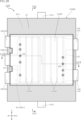
- FIG. 1 is a perspective view of a semiconductor module according to a first embodiment of the present disclosure.
- FIG. 2 is a plan view of the semiconductor module shown in FIG.
- FIG. 3 is a right side view of the semiconductor module shown in FIG.
- FIG. 4 is a cross-sectional view taken along line IV-IV in FIG.
- FIG. 5 is a cross-sectional view taken along line VV in FIG.
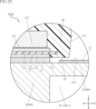
- FIG. 6 is a partially enlarged view of FIG.
- FIG. 7 is a partially enlarged view of FIG.
- FIG. 8 is a plan view of a semiconductor device included in the semiconductor module shown in FIG.
- FIG. 9 is a plan view corresponding to FIG. 8, seen through the sealing resin.
- FIG. 10 is a partially enlarged view of FIG.
- FIG. 11 is a plan view corresponding to FIG.
- FIG. 12 is a right side view of the semiconductor device shown in FIG.
- FIG. 13 is a bottom view of the semiconductor device shown in FIG.
- FIG. 14 is a cross-sectional view taken along line XIV-XIV in FIG.
- FIG. 15 is a cross-sectional view taken along line XV-XV in FIG.
- FIG. 16 is a partial enlarged view of the first element and its periphery shown in FIG.
- FIG. 17 is a partial enlarged view of the second element and its periphery shown in FIG.
- FIG. 18 is a cross-sectional view taken along line XVIII-XVIII in FIG.
- FIG. 19 is a cross-sectional view taken along line XIX-XIX in FIG.
- FIG. 20 is a plan view of a semiconductor module according to the second embodiment of the present disclosure.
- FIG. 21 is a cross-sectional view taken along line XXI-XXI in FIG.
- FIG. 22 is a cross-sectional view taken along line XXII-XXII in FIG.
- FIG. 23 is a partially enlarged view of FIG.
- FIG. 24 is a plan view of a semiconductor module according to a third embodiment of the present disclosure.
- FIG. 25 is a cross-sectional view taken along line XXV-XXV in FIG.
- FIG. 26 is a cross-sectional view taken along line XXVI-XXVI in FIG.
- FIG. 27 is a partially enlarged view of FIG.
- FIG. 28 is a plan view of a semiconductor module according to a fourth embodiment of the present disclosure.
- FIG. 29 is a cross-sectional view taken along line XXIX-XXIX in FIG.
- FIG. 30 is a plan view of a semiconductor module according to a fifth embodiment of the present disclosure.
- FIG. 31 is a cross-sectional view taken along line XXI-XXXI in FIG.
- FIG. 32 is a cross-sectional view taken along line XXII-XXXII in FIG.
- the semiconductor module A10 may include a semiconductor device B, a bonding layer 71, a cover layer 72, a frame 73, and a heat dissipation member 80.
- the normal direction of the first main surface 121A of the first conductive layer 121 of the semiconductor device B described below is referred to as the "first direction z.”
- the direction perpendicular to the first direction z is referred to as the "second direction x.”
- the direction perpendicular to the first direction z and the second direction x is referred to as the "third direction y.”
- the semiconductor device B may include a substrate 11, a first conductive layer 121, a second conductive layer 122, a first power terminal 13, a second power terminal 14, a third power terminal 15, a first signal terminal 161, a second signal terminal 162, a plurality of semiconductor elements 21, a first conductive member 31, a second conductive member 32, and a sealing resin 50.
- the semiconductor device B may further include a third signal terminal 171, a fourth signal terminal 172, a pair of fifth signal terminals 181, a pair of sixth signal terminals 182, a seventh signal terminal 19, a pair of thermistors 22, and a pair of control wirings 60.
- FIG. 9 the sealing resin 50 is shown through for ease of understanding.
- the through sealing resin 50 is shown by an imaginary line (two-dot chain line).
- FIG. 11 shows the first conductive member 31 through a see-through view, and omits the second conductive member 32 and the sealing resin 50.
- the see-through first conductive member 31 is shown by an imaginary line.
- line XV-XV is shown by a dashed line.
- the semiconductor device B can be configured to convert the DC power supply voltage applied to the first power terminal 13 and the third power terminal 15 into AC power using multiple semiconductor elements 21.
- the converted AC power can be input from the second power terminal 14 to a power supply target such as a motor.
- the substrate 11 may be located on the opposite side of the multiple semiconductor elements 21 in the first direction z, with the first conductive layer 121 and the second conductive layer 122 sandwiched therebetween.
- the substrate 11 may support the first conductive layer 121 and the second conductive layer 122.
- the substrate 11 may be composed of a DBC (Direct Bonded Copper) substrate.
- the substrate 11 may include an insulating layer 111, a pair of metal layers 112, and a heat dissipation layer 113.
- the substrate 11 may be covered with a sealing resin 50 except for a portion of the heat dissipation layer 113.
- the insulating layer 111 may include a portion interposed between the metal layer 112 and the heat dissipation layer 113 in the first direction z.
- the insulating layer 111 may be made of a material with relatively high thermal conductivity.
- the insulating layer 111 may be made of ceramics including a sintered body of aluminum nitride (AlN), for example.
- the insulating layer 111 may be made of ceramics or an insulating resin sheet. The thickness of the insulating layer 111 may be thinner than the thickness of each of the first conductive layer 121 and the second conductive layer 122.
- the pair of metal layers 112 may be located between the insulating layer 111 and the first conductive layer 121 and the second conductive layer 122 in the first direction z.
- the composition of the pair of metal layers 112 may include copper (Cu).
- Cu copper
- each of the pair of metal layers 112 may be surrounded by the periphery of the insulating layer 111.
- the heat dissipation layer 113 may be located on the opposite side to the metal layer 112 in the first direction z, with the insulating layer 111 sandwiched therebetween. As shown in Figure 13, the heat dissipation layer 113 may be exposed from the sealing resin 50.
- the composition of the heat dissipation layer 113 may include copper.
- the thickness of the heat dissipation layer 113 may be greater than the thickness of the insulating layer 111. When viewed in the first direction z, the heat dissipation layer 113 may be surrounded by the periphery of the insulating layer 111.
- the first conductive layer 121 and the second conductive layer 122 may be bonded to the substrate 11 as shown in Figures 15 to 17.
- the composition of the first conductive layer 121 and the second conductive layer 122 may include copper.
- the first conductive layer 121 and the second conductive layer 122 may be separated from each other in the second direction x.
- the first conductive layer 121 may have a first main surface 121A facing the first direction z.
- the first main surface 121A faces the multiple semiconductor elements 21.
- the first conductive layer 121 may be bonded to one of the pair of metal layers 112 via the bonding layer 123.
- the bonding layer 123 may be, for example, a brazing material containing silver (Ag) in its composition.
- the second conductive layer 122 may have a second main surface 122A facing the first direction z.
- the second main surface 122A can face the same side as the first main surface 121A in the first direction z.
- the second conductive layer 122 can be bonded to the other metal layer 112 of the pair of metal layers 112 via a bonding layer 123.
- the dimensions of each of the first conductive layer 121 and the second conductive layer 122 in the first direction z can be larger than the dimension of the base material 11 in the first direction z.
- Each of the multiple semiconductor elements 21 may be mounted on either the first conductive layer 121 or the second conductive layer 122, as shown in Figures 11 and 15.
- the multiple semiconductor elements 21 may be, for example, MOSFETs (Metal-Oxide-Semiconductor Field-Effect Transistors).
- the multiple semiconductor elements 21 may be switching elements such as IGBTs (Insulated Gate Bipolar Transistors), diodes, etc.
- the semiconductor element 21 may be an n-channel MOSFET with a vertical structure.
- the multiple semiconductor elements 21 may include a compound semiconductor substrate.
- the composition of the compound semiconductor substrate may include silicon carbide (SiC).
- the multiple semiconductor elements 21 may include multiple first elements 21A and multiple second elements 21B.
- the structure of each of the multiple second elements 21B may be the same as the structure of each of the multiple first elements 21A.
- the multiple first elements 21A may be mounted on the first main surface 121A of the first conductive layer 121.
- the multiple first elements 21A may be arranged along the third direction y.
- the multiple second elements 21B may be mounted on the second main surface 122A of the second conductive layer 122.
- the multiple second elements 21B may be arranged along the third direction y.
- each of the multiple semiconductor elements 21 can have a first electrode 211, a second electrode 212, a third electrode 213 and a fourth electrode 214.
- the first electrode 211 may face either the first conductive layer 121 or the second conductive layer 122. A current corresponding to the power before being converted by the semiconductor element 21 may flow through the first electrode 211. In other words, the first electrode 211 may correspond to the drain electrode of the semiconductor element 21.
- the second electrode 212 may be located on the opposite side to the first electrode 211 in the first direction z. A current corresponding to the power converted by the semiconductor element 21 may flow through the second electrode 212. In other words, the second electrode 212 may correspond to the source electrode of the semiconductor element 21.
- the third electrode 213 may be located on the same side as the second electrode 212 in the first direction z.
- a gate voltage for driving the semiconductor element 21 may be applied to the third electrode 213.
- the third electrode 213 may correspond to the gate electrode of the semiconductor element 21.
- the area of the third electrode 213 may be smaller than the area of the second electrode 212 when viewed in the first direction z.
- the fourth electrode 214 may be located on the same side as the second electrode 212 in the first direction z, and next to the third electrode 213 in the third direction y.
- the potential of the fourth electrode 214 may be equal to the potential of the second electrode 212.
- the conductive bonding layer 23 may be interposed between any one of the first conductive layer 121 and the second conductive layer 122 and the first electrode 211 of any one of the multiple semiconductor elements 21.
- the conductive bonding layer 23 may be, for example, solder.
- the conductive bonding layer 23 may be configured to include a sintered body of metal particles.
- the first electrodes 211 of the multiple first elements 21A may be conductively bonded to the first main surface 121A of the first conductive layer 121 via the conductive bonding layer 23. As a result, the first electrodes 211 of the multiple first elements 21A may be electrically connected to the first conductive layer 121.
- the first electrodes 211 of the multiple second elements 21B may be conductively bonded to the second main surface 122A of the second conductive layer 122 via the conductive bonding layer 23. As a result, the first electrodes 211 of the multiple second elements 21B may be electrically connected to the second conductive layer 122.
- the first power terminal 13 may be located on the opposite side of the second conductive layer 122 in the second direction x with the first conductive layer 121 therebetween, and may be connected to the first conductive layer 121. As a result, the first power terminal 13 may be electrically connected to the first electrodes 211 of the multiple first elements 21A via the first conductive layer 121.
- the first power terminal 13 may be a P terminal (positive electrode) to which a DC power supply voltage to be the subject of power conversion is applied.
- the first power terminal 13 may extend from the first conductive layer 121 in the second direction x.
- the first power terminal 13 may have a covering portion 13A and an exposed portion 13B. As shown in FIG.
- the covering portion 13A may be connected to the first conductive layer 121 and may be covered with a sealing resin 50.
- the covering portion 13A may be flush with the first main surface 121A of the first conductive layer 121.
- the exposed portion 13B extends from the covered portion 13A in the second direction x and can be exposed from the sealing resin 50.
- the second power terminal 14 may be located on the opposite side of the first conductive layer 121 in the second direction x with the second conductive layer 122 therebetween, and may be connected to the second conductive layer 122. As a result, the second power terminal 14 may be electrically connected to the first electrodes 211 of the multiple second elements 21B via the second conductive layer 122. AC power converted by the multiple semiconductor elements 21 may be output from the second power terminal 14.
- the second power terminal 14 may include a pair of regions separated from each other in the third direction y. Alternatively, the second power terminal 14 may have a single configuration that does not include a pair of regions.
- the second power terminal 14 may have a covering portion 14A and an exposed portion 14B. As shown in FIG.
- the covering portion 14A may be connected to the second conductive layer 122 and may be covered with the sealing resin 50.
- the covering portion 14A may be flush with the second main surface 122A of the second conductive layer 122.
- the exposed portion 14B extends from the covered portion 14A in the second direction x and can be exposed from the sealing resin 50.
- the third power terminal 15 may be located on the same side as the first power terminal 13 with respect to the first conductive layer 121 and the second conductive layer 122 in the second direction x, and may be separated from the first conductive layer 121 and the second conductive layer 122.
- the third power terminal 15 may be electrically connected to the second electrodes 212 of the multiple second elements 21B.
- the third power terminal 15 may be an N terminal (negative electrode) to which a DC power supply voltage to be the subject of power conversion is applied.
- the third power terminal 15 may include a pair of regions separated from each other in the third direction y.
- the first power terminal 13 may be located between the pair of regions in the third direction y.
- the third power terminal 15 may have a covering portion 15A and an exposed portion 15B. As shown in Figure 14, the covering portion 15A may be separated from the first conductive layer 121 and may be covered with a sealing resin 50. The exposed portion 15B extends from the covered portion 15A in the second direction x and can be exposed from the sealing resin 50
- the pair of control wirings 60 may constitute a part of the conductive path between the first signal terminal 161, the second signal terminal 162, the third signal terminal 171, the fourth signal terminal 172, the pair of fifth signal terminals 181, the pair of sixth signal terminals 182, and the multiple semiconductor elements 21.
- the pair of control wirings 60 may include a first wiring 601 and a second wiring 602. In the second direction x, the first wiring 601 may be located between the multiple first elements 21A and the first power terminal 13 and the third power terminal 15.
- the first wiring 601 may be joined to the first main surface 121A of the first conductive layer 121.
- the first wiring 601 may also constitute a part of the conductive path between the seventh signal terminal 19 and the first conductive layer 121.
- the second wiring 602 may be located between the multiple second elements 21B and the second power terminal 14.
- the second wiring 602 can be bonded to the second main surface 122A of the second conductive layer 122.
- the pair of control wiring 60 can have an insulating layer 61, multiple wiring layers 62, a metal layer 63, and multiple sleeves 64.
- the pair of control wiring 60 can be covered with the sealing resin 50 except for a portion of each of the multiple sleeves 64.
- the insulating layer 61 may include a portion interposed between the multiple wiring layers 62 and the metal layer 63 in the first direction z.
- the insulating layer 61 may be made of ceramics, for example.
- the insulating layer 61 may be made of a material other than ceramics, such as an insulating resin sheet.
- the multiple wiring layers 62 may be located on one side of the insulating layer 61 in the first direction z.
- the composition of the multiple wiring layers 62 may include copper.
- the multiple wiring layers 62 may include a first wiring layer 621, a second wiring layer 622, a pair of third wiring layers 623, a fourth wiring layer 624, and a fifth wiring layer 625.
- the pair of third wiring layers 623 may be adjacent to each other in the third direction y.
- the metal layer 63 may be located on the opposite side to the multiple wiring layers 62 in the first direction z, with the insulating layer 61 sandwiched therebetween.
- the composition of the metal layer 63 may include copper.
- the metal layer 63 of the first wiring 601 may be bonded to the first main surface 121A of the first conductive layer 121 by a first adhesive layer 68.
- the metal layer 63 of the second wiring 602 may be bonded to the second main surface 122A of the second conductive layer 122 by a first adhesive layer 68.
- the first adhesive layer 68 may be a material that may or may not be conductive.
- the first adhesive layer 68 may be, for example, solder.
- each of the multiple sleeves 64 may be bonded to one of the multiple wiring layers 62 by a second adhesive layer 69.
- the multiple sleeves 64 may be made of a conductive material such as metal.
- Each of the multiple sleeves 64 may be tubular and extend along the first direction z.
- One end of the multiple sleeves 64 may be conductively bonded to one of the multiple wiring layers 62.
- an end surface 641 corresponding to the other end of the multiple sleeves 64 may be exposed from the top surface 51 of the sealing resin 50 described later.
- the second adhesive layer 69 may be conductive.
- the second adhesive layer 69 may be, for example, solder.
- One of the pair of thermistors 22 may be conductively joined to a pair of third wiring layers 623 of the first wiring 601 as shown in FIG. 10.
- the other of the pair of thermistors 22 may be conductively joined to a pair of third wiring layers 623 of the second wiring 602 as shown in FIG. 10.
- the pair of thermistors 22 may be, for example, NTC (Negative Temperature Coefficient) thermistors.
- NTC thermistors may have the property that their resistance decreases gradually with increasing temperature.
- the pair of thermistors 22 may be used as a temperature detection sensor for the semiconductor device B.
- the first signal terminal 161, the second signal terminal 162, the third signal terminal 171, the fourth signal terminal 172, the pair of fifth signal terminals 181, the pair of sixth signal terminals 182, and the seventh signal terminal 19 may each be a metal pin extending in the first direction z, as shown in FIG. 1. These terminals may protrude from the top surface 51 of the sealing resin 50 described below. Furthermore, these terminals may be individually pressed into the multiple sleeves 64 of the pair of control wiring 60. As a result, each of these terminals may be supported by one of the multiple sleeves 64 and be conductive to one of the multiple wiring layers 62.
- the first signal terminal 161 can be press-fitted into one of the multiple sleeves 64 of the pair of control wires 60 that is joined to the first wiring layer 621 of the first wire 601. As a result, the first signal terminal 161 can be supported by the sleeve 64 and can be electrically connected to the first wiring layer 621 of the first wire 601. Furthermore, the first signal terminal 161 can be electrically connected to the third electrodes 213 of the multiple first elements 21A. A gate voltage for driving the multiple first elements 21A can be applied to the first signal terminal 161.
- the second signal terminal 162 can be press-fitted into one of the multiple sleeves 64 of the pair of control wirings 60 that is joined to the first wiring layer 621 of the second wiring 602.
- the second signal terminal 162 can be supported by the sleeve 64 and can be electrically connected to the first wiring layer 621 of the second wiring 602.
- the second signal terminal 162 can be electrically connected to the third electrodes 213 of the multiple second elements 21B.
- a gate voltage for driving the multiple second elements 21B can be applied to the second signal terminal 162.
- the third signal terminal 171 may be located next to the first signal terminal 161 in the third direction y. As shown in FIG. 11, the third signal terminal 171 may be press-fitted into one of the multiple sleeves 64 of the pair of control wirings 60 that is joined to the second wiring layer 622 of the first wiring 601. As a result, the third signal terminal 171 may be supported by the sleeve 64 and may be conductive to the second wiring layer 622 of the first wiring 601. Furthermore, the third signal terminal 171 may be conductive to the fourth electrodes 214 of the multiple first elements 21A. A voltage corresponding to the maximum current among the currents flowing through the fourth electrodes 214 of the multiple first elements 21A may be applied to the third signal terminal 171.
- the fourth signal terminal 172 may be located next to the second signal terminal 162 in the third direction y, as shown in FIG. 8.
- the fourth signal terminal 172 may be press-fitted into one of the multiple sleeves 64 of the pair of control wirings 60 that is joined to the second wiring layer 622 of the second wiring 602, as shown in FIG. 11. This allows the fourth signal terminal 172 to be supported by the sleeve 64 and to be conductive to the second wiring layer 622 of the second wiring 602.
- the fourth signal terminal 172 may be conductive to the fourth electrodes 214 of the multiple second elements 21B. A voltage corresponding to the maximum current among the currents flowing through the fourth electrodes 214 of the multiple second elements 21B may be applied to the fourth signal terminal 172.
- the pair of fifth signal terminals 181 may be located on the opposite side to the third signal terminal 171 in the third direction y, sandwiching the first signal terminal 161 therebetween.
- the pair of fifth signal terminals 181 may be adjacent to each other in the third direction y.
- the pair of fifth signal terminals 181 may be individually pressed into a pair of sleeves 64 that are joined to a pair of third wiring layers 623 of the first wiring 601, among the multiple sleeves 64 of the pair of control wirings 60.
- the pair of fifth signal terminals 181 may be supported by the pair of sleeves 64 and may be conductive to the pair of third wiring layers 623 of the first wiring 601.
- the pair of fifth signal terminals 181 may be conductive to the thermistor 22 that is conductively joined to the pair of third wiring layers 623 of the first wiring 601, among the pair of thermistors 22.
- the pair of sixth signal terminals 182 may be located on the opposite side of the fourth signal terminal 172 in the third direction y, sandwiching the second signal terminal 162 therebetween.
- the pair of sixth signal terminals 182 may be adjacent to each other in the third direction y.
- the pair of sixth signal terminals 182 may be individually pressed into a pair of sleeves 64 that are joined to a pair of third wiring layers 623 of the second wiring 602, among the multiple sleeves 64 of the pair of control wirings 60.
- the pair of sixth signal terminals 182 may be supported by the pair of sleeves 64 and may be conductive to the pair of third wiring layers 623 of the second wiring 602.
- the pair of sixth signal terminals 182 may be conductive to the thermistor 22 that is conductively joined to the pair of third wiring layers 623 of the second wiring 602, among the pair of thermistors 22.
- the seventh signal terminal 19 may be located on the opposite side of the first signal terminal 161 in the third direction y with the third signal terminal 171 sandwiched therebetween. As shown in FIG. 11, the seventh signal terminal 19 may be press-fitted into the sleeve 64 joined to the fifth wiring layer 625 of the first wiring 601, among the multiple sleeves 64 of the pair of control wirings 60. As a result, the seventh signal terminal 19 may be supported by the sleeve 64 and may be conductive to the fifth wiring layer 625 of the first wiring 601. Furthermore, the seventh signal terminal 19 may be conductive to the first conductive layer 121. A voltage equivalent to the DC power input to the first power terminal 13 and the third power terminal 15 may be applied to the seventh signal terminal 19.
- the multiple first wires 41 can be conductively joined to the third electrodes 213 of the multiple first elements 21A and the fourth wiring layer 624 of the first wiring 601 as shown in FIG. 11.
- the multiple third wires 43 can be conductively joined to the fourth wiring layer 624 of the first wiring 601 and the first wiring layer 621 of the first wiring 601 as shown in FIG. 11. This allows the first signal terminal 161 to be electrically connected to the third electrodes 213 of the multiple first elements 21A.
- the composition of the multiple first wires 41 and the multiple third wires 43 can include gold (Au).
- the composition of the multiple first wires 41 and the multiple third wires 43 can include copper or aluminum (Al).
- the multiple first wires 41 can be conductively joined to the third electrodes 213 of the multiple second elements 21B and the fourth wiring layer 624 of the second wiring 602 as shown in FIG. 11.
- the multiple third wires 43 can be conductively joined to the fourth wiring layer 624 of the second wiring 602 and the first wiring layer 621 of the second wiring 602 as shown in FIG. 11. This allows the second signal terminal 162 to be electrically connected to the third electrodes 213 of the multiple second elements 21B.
- the second wires 42 may be conductively bonded to the fourth electrodes 214 of the first elements 21A and the second wiring layer 622 of the first wiring 601, as shown in FIG. 11. This allows the third signal terminal 171 to be electrically connected to the fourth electrodes 214 of the first elements 21A. Furthermore, the second wires 42 may be conductively bonded to the fourth electrodes 214 of the second elements 21B and the second wiring layer 622 of the second wiring 602, as shown in FIG. 11. This allows the fourth signal terminal 172 to be electrically connected to the fourth electrodes 214 of the second elements 21B.
- the composition of the second wires 42 may include gold. Alternatively, the composition of the second wires 42 may include copper or aluminum.
- the fourth wire 44 can be conductively joined to the fifth wiring layer 625 of the first wiring 601 and the first main surface 121A of the first conductive layer 121. This allows the seventh signal terminal 19 to be electrically connected to the first conductive layer 121.
- the composition of the fourth wire 44 can include gold. Alternatively, the composition of the fourth wire 44 can include copper or aluminum.
- the first conductive member 31 may be conductively joined to the second electrodes 212 of the multiple first elements 21A and the second main surface 122A of the second conductive layer 122, as shown in Figures 11 and 16. This allows the second electrodes 212 of the multiple first elements 21A to be conductive to the second conductive layer 122.
- the composition of the first conductive member 31 may include copper.
- the first conductive member 31 may be a metal clip. As shown in Figure 11, the first conductive member 31 may have a main body portion 311, multiple first joint portions 312, multiple first connecting portions 313, second joint portions 314 and second connecting portions 315.
- the main body portion 311 may form a main portion of the first conductive member 31. As shown in FIG. 11, the main body portion 311 may extend in the third direction y. As shown in FIG. 15, the main body portion 311 may straddle between the first conductive layer 121 and the second conductive layer 122.
- the multiple first bonding portions 312 can be individually bonded to the second electrodes 212 of the multiple first elements 21A. Each of the multiple first bonding portions 312 can face the second electrode 212 of one of the multiple first elements 21A.
- the multiple first connecting portions 313 can be connected to the main body portion 311 and the multiple first bonding portions 312.
- the multiple first connecting portions 313 can be separated from each other in the third direction y.
- the multiple first connecting portions 313 when viewed in the third direction y, can be inclined in a direction away from the first main surface 121A of the first conductive layer 121 as they move from the multiple first bonding portions 312 toward the main body portion 311.
- the second joint 314 may be joined to the second main surface 122A of the second conductive layer 122.
- the second joint 314 may face the second main surface 122A.
- the second joint 314 may extend in the third direction y.
- the dimension of the second joint 314 in the third direction y may be equal to the dimension of the main body portion 311 in the third direction y.
- the second connecting portion 315 may be connected to the main body portion 311 and the second joint portion 314.
- the second connecting portion 315 may be inclined in a direction away from the second main surface 122A of the second conductive layer 122 as it moves from the second joint portion 314 toward the main body portion 311.
- the dimension of the second connecting portion 315 in the third direction y may be equal to the dimension of the main body portion 311 in the third direction y.
- the semiconductor device B may further include a first conductive bonding layer 33.
- the first conductive bonding layer 33 may be interposed between the second electrodes 212 of the multiple first elements 21A and the multiple first bonding portions 312.
- the first conductive bonding layer 33 may conductively bond the second electrodes 212 of the multiple first elements 21A to the multiple first bonding portions 312.
- the first conductive bonding layer 33 may be, for example, solder.
- the first conductive bonding layer 33 may include a sintered body of metal particles.
- the semiconductor device B may further include a second conductive bonding layer 34.
- the second conductive bonding layer 34 may be interposed between the second main surface 122A of the second conductive layer 122 and the second bonding portion 314.
- the second conductive bonding layer 34 may conductively bond the second main surface 122A and the second bonding portion 314.
- the second conductive bonding layer 34 may be, for example, solder.
- the second conductive bonding layer 34 may include a sintered body of metal particles.
- the second conductive member 32 may be conductively joined to the second electrodes 212 of the second elements 21B and the covering portion 15A of the third power terminal 15, as shown in FIG. 10 and FIG. 17. This allows the second electrodes 212 of the second elements 21B to be electrically connected to the third power terminal 15.
- the composition of the second conductive member 32 may include copper.
- the second conductive member 32 may be a metal clip. As shown in FIG. 10, the second conductive member 32 may have a pair of main body portions 321, a plurality of third joint portions 322, a plurality of third connecting portions 323, a pair of fourth joint portions 324, a pair of fourth connecting portions 325, a plurality of intermediate portions 326, and a plurality of cross beam portions 327.
- the pair of body portions 321 may be separated from each other in the third direction y.
- the pair of body portions 321 may extend in the second direction x.
- the pair of body portions 321 may be arranged parallel to the first main surface 121A of the first conductive layer 121 and the second main surface 122A of the second conductive layer 122.
- the pair of body portions 321 may be separated from the first main surface 121A and the second main surface 122A by more distance than the body portion 311 of the first conductive member 31.
- the intermediate portions 326 may be spaced apart from one another in the third direction y and positioned between the pair of main body portions 321 in the third direction y.
- the intermediate portions 326 may extend in the second direction x.
- the dimension of each of the intermediate portions 326 in the second direction x may be smaller than the dimension of each of the pair of main body portions 321 in the second direction x.
- the multiple third joints 322 can be individually joined to the second electrodes 212 of the multiple second elements 21B.
- Each of the multiple third joints 322 can face the second electrode 212 of one of the multiple second elements 21B.
- the multiple third connecting portions 323 can be connected to both sides of the multiple third joint portions 322 in the third direction y. Furthermore, the multiple third connecting portions 323 can be connected to either the pair of main body portions 321 or the multiple intermediate portions 326. When viewed in the second direction x, each of the multiple third connecting portions 323 can be inclined in a direction away from the second main surface 122A of the second conductive layer 122 as it moves from one of the multiple third joint portions 322 toward either the pair of main body portions 321 or the multiple intermediate portions 326.
- the pair of fourth joints 324 can be joined to the covering portion 15A of the third power terminal 15.
- the pair of fourth joints 324 can face the covering portion 15A.
- the pair of fourth connecting portions 325 can be connected to the pair of main body portions 321 and the pair of fourth joint portions 324.
- the pair of fourth connecting portions 325 can be inclined in a direction away from the first main surface 121A of the first conductive layer 121 as they move from the pair of fourth joint portions 324 toward the pair of main body portions 321.
- the multiple cross beam portions 327 may be arranged along the third direction y.
- the multiple cross beam portions 327 may include areas that individually overlap the multiple first joint portions 312 of the first conductive member 31.
- the cross beam portion 327 located at the center in the third direction y may be connected to the multiple intermediate portions 326 on both sides in the third direction y.
- the remaining two cross beam portions 327 may be connected to one of the pair of main body portions 321 and one of the multiple intermediate portions 326 on both sides in the third direction y.
- the multiple cross beam portions 327 may be convex toward the side toward which the first main surface 121A of the first conductive layer 121 faces in the first direction z.
- the semiconductor device B may further include a third conductive bonding layer 35.
- the third conductive bonding layer 35 may be interposed between the second electrodes 212 of the multiple second elements 21B and the multiple third bonding portions 322.
- the third conductive bonding layer 35 may conductively bond the second electrodes 212 of the multiple second elements 21B to the multiple third bonding portions 322.
- the third conductive bonding layer 35 may be, for example, solder.
- the third conductive bonding layer 35 may include a sintered body of metal particles.
- the semiconductor device B may further include a fourth conductive bonding layer 36.
- the fourth conductive bonding layer 36 may be interposed between the covering portion 15A of the third power terminal 15 and the pair of fourth joints 324.
- the fourth conductive bonding layer 36 may conductively bond the covering portion 15A and the pair of fourth joints 324.
- the fourth conductive bonding layer 36 may be, for example, solder.
- the fourth conductive bonding layer 36 may include a sintered body of metal particles.
- the sealing resin 50 may cover the first conductive layer 121, the second conductive layer 122, the semiconductor elements 21, the first conductive member 31 and the second conductive member 32. Furthermore, the sealing resin 50 may cover a portion of each of the substrate 11, the first power terminal 13, the second power terminal 14 and the third power terminal 15.
- the sealing resin 50 may have electrical insulation properties.
- the sealing resin 50 may be a material containing, for example, a black epoxy resin. As shown in Figures 8 and 12 to 15, the sealing resin 50 may have a top surface 51, a bottom surface 52, a pair of first side surfaces 53, a pair of second side surfaces 54 and a pair of recesses 55.
- the top surface 51 may face the same side as the first main surface 121A of the first conductive layer 121 in the first direction z.
- the bottom surface 52 may face the opposite side to the top surface 51 in the first direction z.
- the heat dissipation layer 113 of the substrate 11 may be exposed from the bottom surface 52.
- the pair of first side surfaces 53 may be separated from each other in the second direction x.
- the pair of first side surfaces 53 may face the second direction x and extend in the third direction y.
- the pair of first side surfaces 53 may be connected to the top surface 51.
- the exposed portion 13B of the first power terminal 13 and the exposed portion 15B of the third power terminal 15 may be exposed from one of the pair of first side surfaces 53.
- the exposed portion 14B of the second power terminal 14 may be exposed from the other of the pair of first side surfaces 53.
- the pair of second side surfaces 54 may be separated from each other in the third direction y.
- the pair of second side surfaces 54 may face opposite each other in the third direction y and extend in the second direction x.
- the pair of second side surfaces 54 may be connected to the top surface 51 and the bottom surface 52.
- the pair of recesses 55 may be recessed in the second direction x from the first side surfaces 53 on which the exposed portion 13B of the first power terminal 13 and the exposed portion 15B of the third power terminal 15 are exposed.
- the pair of recesses 55 may extend from the top surface 51 to the bottom surface 52 in the first direction z.
- the pair of recesses 55 may be located on both sides of the first power terminal 13 in the third direction y.
- the heat dissipation member 80 can be used to cool the semiconductor device B.
- the heat dissipation member 80 can contain a metal.
- the heat dissipation member 80 can be made of a material containing aluminum, for example.
- the base material 11 can be located on one side of the heat dissipation member 80 in the first direction z, and can be joined to the heat dissipation member 80.
- the bottom surface 52 of the sealing resin 50 can face the heat dissipation member 80.
- the heat dissipation member 80 may have a housing 81 and a heat sink 82.
- the housing 81 may have a hollow portion 811, an inlet 812, and an outlet 813.
- the hollow portion 811 may be located inside the housing 81.
- the inlet 812 and the outlet 813 may be connected to the hollow portion 811.
- the inlet 812 and the outlet 813 may be located on opposite sides of the hollow portion 811 in the third direction y.
- the heat dissipation member 80 may be configured so that the refrigerant flows from the inlet 812 through the hollow portion 811 to the outlet 813.
- the housing 81 may have a mounting surface 81A facing the first direction z.
- the mounting surface 81A may face the heat dissipation layer 113 of the base material 11.
- the hollow portion 811 of the housing 81 may include a sudden contraction portion 811A.
- the sudden contraction portion 811A is a portion that is perpendicular to the first direction z and that is a portion of the hollow portion 811 in the section from the inlet 812 to the outlet 813 where the cross-sectional area is the smallest.
- the heat sink 82 may be housed in the sudden contraction portion 811A of the hollow portion 811 of the housing 81.
- the heat sink 82 may be connected to the housing 81.
- the heat sink 82 may be a plurality of fins spaced apart from each other in the second direction x.
- each of the plurality of fins may extend in the third direction y.
- each of the plurality of fins may extend in a direction perpendicular to the first direction z and along the section from the inlet 812 to the outlet 813.
- each of the first conductive layer 121 and the second conductive layer 122 can overlap the sudden contraction portion 811A of the hollow portion 811 of the housing 81. Furthermore, when viewed in the first direction z, each of the first conductive layer 121 and the second conductive layer 122 can overlap the heat sink 82.
- the bonding layer 71 can bond the mounting surface 81A of the housing 81 to the heat dissipation layer 113 of the base material 11.
- the bonding layer 71 can contain a metal.
- the bonding layer 71 can be formed by sintering metal particles containing silver or the like, solder bonding, or solid-state diffusion bonding.
- the bonding layer 71 can have an end surface 71A that faces a direction perpendicular to the first direction z.
- the frame body 73 may rise from the heat dissipation member 80 in the first direction z toward the side where the first power terminal 13, the second power terminal 14, and the third power terminal 15 are located.
- the frame body 73 may be an insulator.
- the frame body 73 may include, for example, a resin.
- the frame body 73 may be joined to the housing 81 along the periphery of the mounting surface 81A of the housing 81.
- the frame body 73 may surround each of the sealing resin 50 and the coating layer 72.
- the frame body 73 may overlap each of the pair of first side surfaces 53 of the sealing resin 50 and the pair of second side surfaces 54 of the sealing resin 50.
- the covering layer 72 may cover a part of the heat dissipation member 80 as shown in FIG. 1, FIG. 2, FIG. 4, and FIG. 5.
- the covering layer 72 may be located on the side of the heat dissipation member 80 where the base material 11 is located in the first direction z.
- the covering layer 72 may cover the mounting surface 81A of the housing 81 and the bottom surface 52 of the sealing resin 50, and may be in contact with each of the pair of first side surfaces 53 and the pair of second side surfaces 54 of the sealing resin 50.
- the covering layer 72 may be in contact with the end surface 71A of the bonding layer 71.
- the linear expansion coefficient of the covering layer 72 may be greater than the linear expansion coefficient of the bonding layer 71.
- the covering layer 72 may be in contact with the frame body 73.
- the dimension of the covering layer 72 in the first direction z may be equal to the dimension of the frame body 73 in the first direction z.
- the covering layer 72 may surround each of the bonding layer 71 and the sealing resin 50.
- each of the first power terminal 13, the second power terminal 14, and the third power terminal 15 may overlap each of the heat dissipation member 80 and the covering layer 72.
- the covering layer 72 may be separated from each of the first power terminal 13, the second power terminal 14, and the third power terminal 15.
- the sealing resin 50 may overlap the covering layer 72.
- the covering layer 72 can be formed by the following procedure. First, the semiconductor device B is bonded to the mounting surface 81A of the housing 81 via the bonding layer 71. At this time, the heat dissipation layer 113 of the base material 11 is bonded to the mounting surface 81A. Next, the frame body 73 is bonded to the mounting surface 81A. At this time, the frame body 73 is not in contact with each of the first power terminal 13, the second power terminal 14, and the third power terminal 15. Next, using a dispenser or the like, molten resin material is poured onto the mounting surface 81A surrounded by the frame body 73. In this case, each of the pair of first side surfaces 53 of the sealing resin 50 and the pair of second side surfaces 54 of the sealing resin 50 is covered with the resin material. Finally, the resin material is hardened to complete the formation of the covering layer 72.
- the semiconductor module A10 may include a heat dissipation member 80, a semiconductor device B bonded to the heat dissipation member 80, and a coating layer 72 that covers a portion of the heat dissipation member 80 and is an insulator.
- the semiconductor device B may include a base material 11 located on one side of the heat dissipation member 80 in the first direction z and bonded to the heat dissipation member 80, a first conductive layer 121, a semiconductor element 21 (first element 21A), a sealing resin 50, and a first power terminal 13 that is conductive to the first conductive layer 121 and the semiconductor element 21 and includes a portion that protrudes from the sealing resin 50 to the outside in a direction perpendicular to the first direction z.
- the coating layer 72 may be located on the one side of the heat dissipation member 80 in the first direction z. When viewed in the first direction z, the first power terminal 13 may overlap each of the heat dissipation member 80 and the coating layer 72. With this configuration, heat generated by the semiconductor device B is released to the outside from the base material 11 through the heat dissipation member 80, and the creepage distance from the first power terminal 13 to the heat dissipation member 80 can be extended by the coating layer 72. Therefore, with this configuration, in the semiconductor module A10, it is possible to increase the cooling efficiency of the semiconductor device B while suppressing a decrease in the dielectric strength voltage of the semiconductor device B.
- the sealing resin 50 When viewed in the first direction z, the sealing resin 50 can overlap the coating layer 72. This configuration can further extend the creepage distance from the first power terminal 13 to the heat dissipation member 80. This can effectively prevent a decrease in the dielectric strength voltage of the semiconductor device B.
- the semiconductor module A10 may further include a bonding layer 71 that bonds the mounting surface 81A of the heat dissipation member 80 to the base material 11 and contains a metal.
- the covering layer 72 may be in contact with the bonding layer 71.
- thermal strain may occur in the bonding layer 71 due to heat generated from the semiconductor device B.
- the thermal strain concentrated in the bonding layer 71 is reduced by the covering layer 72, so that the thermal strain in the bonding layer 71 can be suppressed. This makes it possible to suppress cracks that occur in the bonding layer 71.
- the linear expansion coefficient of the covering layer 72 is greater than the linear expansion coefficient of the bonding layer 71.
- the sealing resin 50 may have a bottom surface 52 that faces the heat dissipation member 80 in the first direction z.
- the covering layer 72 may cover the bottom surface 52. This configuration sufficiently extends the creepage distance from the first power terminal 13 to the bonding layer 71, and improves the bonding strength between the heat dissipation member 80 and the semiconductor device B.
- the sealing resin 50 may have a pair of first side surfaces 53 and a pair of second side surfaces 54 that face in a direction perpendicular to the first direction z.
- the covering layer 72 may contact each of the pair of first side surfaces 53 and the pair of second side surfaces 54. This configuration may further increase the creepage distance from the first power terminal 13 to the heat dissipation member 80. In this case, the creepage distance can be more effectively increased by configuring the covering layer 72 to surround the sealing resin 50 when viewed in the first direction z.
- the semiconductor module A10 may further include a frame body 73 which rises from the heat dissipation member 80 in the first direction z towards the side where the first power terminal 13 is located and is an insulator. As viewed in the first direction z, the frame body 73 may surround the coating layer 72. With this configuration, when forming the coating layer 72, the frame body 73 can restrict excessive spreading of the molten resin material. Furthermore, the frame body 73 makes it easy to adjust the dimension of the coating layer 72 in the first direction z.
- each of the first conductive layer 121 and the second conductive layer 122 in the first direction z can be made larger than the dimension of the substrate 11 in the first direction z. This configuration makes it easier for heat to diffuse in each of the first conductive layer 121 and the second conductive layer 122 in a direction perpendicular to the first direction z. This reduces the thermal resistance of each of the first conductive layer 121 and the second conductive layer 122 in the first direction z.
- the heat dissipation member 80 may have a housing 81 including a mounting surface 81A.
- the housing 81 may have a hollow portion 811 located inside the housing 81, and an inlet 812 and an outlet 813 leading to the hollow portion 811.
- the first conductive layer 121 may overlap the hollow portion 811. With this configuration, a coolant can be caused to flow through the hollow portion 811, thereby improving the cooling efficiency of the semiconductor device B.
- the hollow portion 811 of the housing 81 may include a sudden contraction portion 811A that is perpendicular to the first direction z and has a minimum cross-sectional area in the section from the inlet 812 to the outlet 813.
- the first conductive layer 121 may overlap the sudden contraction portion 811A. This configuration can increase the flow rate of the refrigerant in the sudden contraction portion 811A, thereby further improving the cooling efficiency of the semiconductor device B.
- the heat dissipation member 80 may have a heat sink 82 that is housed in the sudden contraction portion 811A of the housing 81 and is connected to the housing 81. When viewed in the first direction z, each of the first conductive layer 121 and the second conductive layer 122 may overlap the heat sink 82. This configuration increases the contact area of the heat dissipation member 80 with the refrigerant, thereby further improving the cooling efficiency of the semiconductor device B.
- the heat dissipation body 82 may include a plurality of fins. Each of the plurality of fins may extend in a direction perpendicular to the first direction z and along the section from the inlet 812 to the outlet 813. This configuration can suppress the obstruction of the flow of the refrigerant in the sudden contraction section 811A of the heat dissipation member 80.
- a semiconductor module A20 according to a second embodiment of the present disclosure will be described with reference to Figures 20 to 23.
- elements that are the same as or similar to those in the semiconductor module A10 described above are given the same reference numerals and duplicated descriptions will be omitted.
- Semiconductor module A20 differs from semiconductor module A10 in that it does not have a frame body 73 and in the configuration of the covering layer 72.
- the covering layer 72 can reach the entire periphery of the mounting surface 81A of the housing 81.
- the covering layer 72 can be made of a resin sheet or a material including ceramics.
- the covering layer 72 can be separated from each of the pair of first side surfaces 53 of the sealing resin 50 and the pair of second side surfaces 54 of the sealing resin 50.
- the sealing resin 50 can overlap the covering layer 72.
- the covering layer 72 can surround each of the bonding layer 71 and the sealing resin 50.
- the covering layer 72 can also be separated from each of the end surface 71A of the bonding layer 71 and the bottom surface 52 of the sealing resin 50.
- the dimension of the covering layer 72 in the first direction z can be smaller than the dimension of the bonding layer 71 in the first direction z.
- the semiconductor module A20 may include a heat dissipation member 80, a semiconductor device B bonded to the heat dissipation member 80, and a coating layer 72 that covers a portion of the heat dissipation member 80 and is an insulator.
- the semiconductor device B may include a base material 11 located on one side of the heat dissipation member 80 in the first direction z and bonded to the heat dissipation member 80, a first conductive layer 121, a semiconductor element 21 (first element 21A), a sealing resin 50, and a first power terminal 13 that is conductive to the first conductive layer 121 and the semiconductor element 21 and includes a portion that protrudes from the sealing resin 50 to the outside in a direction perpendicular to the first direction z.
- the coating layer 72 may be located on the one side of the heat dissipation member 80 in the first direction z.
- the first power terminal 13 may overlap each of the heat dissipation member 80 and the coating layer 72. Therefore, according to this configuration, even in the semiconductor module A20, it is possible to suppress a decrease in the insulation withstand voltage of the semiconductor device B while increasing the cooling efficiency of the semiconductor device B. Furthermore, the semiconductor module A20 has a common configuration with the semiconductor module A10, and therefore provides the same effects as the semiconductor module A10.
- a semiconductor module A30 according to a third embodiment of the present disclosure will be described with reference to Figures 24 to 27.
- elements that are the same as or similar to those in the semiconductor module A10 described above are given the same reference numerals, and duplicated descriptions will be omitted.
- Semiconductor module A30 differs from semiconductor module A10 in that it does not have a frame body 73 and in the configuration of the coating layer 72 and heat dissipation member 80.
- the housing 81 may have a groove 814 located outward from the bonding layer 71 when viewed in the first direction z and recessed from the mounting surface 81A of the housing 81.
- the groove 814 may surround each of the bonding layer 71 and the sealing resin 50. At least a portion of the covering layer 72 may be accommodated in the groove 814.
- each of the first power terminal 13, the second power terminal 14, the third power terminal 15, and the sealing resin 50 may overlap the groove 814.
- the mounting surface 81A may include an area that is not covered by the covering layer 72 and is exposed to the outside.
- the covering layer 72 covers the bottom surface 52 of the sealing resin 50 and may contact each of the pair of first side surfaces 53 and the pair of second side surfaces 54 of the sealing resin 50. As shown in FIG. 27, the covering layer 72 may contact the end surface 71A of the bonding layer 71. A portion of the covering layer 72 may bulge in the first direction z and protrude from the groove portion 814 of the housing 81.
- the covering layer 72 may be formed by bonding the semiconductor device B to the mounting surface 81A of the housing 81 via the bonding layer 71, and then pouring molten resin material into the groove portion 814 of the housing 81 using a dispenser or the like.
- the semiconductor module A30 may include a heat dissipation member 80, a semiconductor device B bonded to the heat dissipation member 80, and a coating layer 72 that covers a portion of the heat dissipation member 80 and is an insulator.
- the semiconductor device B may include a base material 11 located on one side of the heat dissipation member 80 in the first direction z and bonded to the heat dissipation member 80, a first conductive layer 121, a semiconductor element 21 (first element 21A), a sealing resin 50, and a first power terminal 13 that is conductive to the first conductive layer 121 and the semiconductor element 21 and includes a portion that protrudes from the sealing resin 50 to the outside in a direction perpendicular to the first direction z.
- the coating layer 72 may be located on the one side of the heat dissipation member 80 in the first direction z.
- the first power terminal 13 may overlap each of the heat dissipation member 80 and the coating layer 72. Therefore, according to this configuration, even in the semiconductor module A30, it is possible to suppress a decrease in the insulation withstand voltage of the semiconductor device B while increasing the cooling efficiency of the semiconductor device B. Furthermore, the semiconductor module A30 has a common configuration with the semiconductor module A10, and therefore provides the same effects as the semiconductor module A10.
- the heat dissipation member 80 is located outward of the bonding layer 71 when viewed in the first direction z, and may have a groove portion 814 recessed from the mounting surface 81A of the housing 81. At least a portion of the coating layer 72 may be accommodated in the groove portion 814. By adopting this configuration, the coating layer 72 can be formed from molten resin material without the need for a frame body 73.
- a portion of the coating layer 72 may bulge in the first direction z and protrude from the groove portion 814.
- the coating layer 72 may cover the bottom surface 52 of the sealing resin 50, and may be in contact with the bonding layer 71, the pair of first side surfaces 53 of the sealing resin 50, and the pair of second side surfaces 54 of the sealing resin 50. This can suppress both a decrease in the dielectric strength of the semiconductor device B and the occurrence of cracks in the bonding layer 71 due to heat generated by the semiconductor device B.
- a semiconductor module A40 according to a fourth embodiment of the present disclosure will be described with reference to Fig. 28 and Fig. 29.
- elements that are the same as or similar to those of the semiconductor module A10 described above are denoted by the same reference numerals, and duplicated descriptions will be omitted.
- the configuration of coating layer 72 and frame body 73 differs from that of semiconductor module A10.
- the area of the covering layer 72 can be smaller than the area of the covering layer 72 of the semiconductor module A10 when viewed in the first direction z.
- the extension of the frame body 73 can be shorter than the extension of the frame body 73 of the semiconductor module A10 depending on the shape of the covering layer 72.
- the area of the mounting surface 81A of the housing 81 that does not overlap any of the first power terminal 13, the second power terminal 14, and the third power terminal 15 of the semiconductor device B when viewed in the first direction z can be exposed to the outside.
- the semiconductor module A40 may include a heat dissipation member 80, a semiconductor device B bonded to the heat dissipation member 80, and a coating layer 72 that covers a portion of the heat dissipation member 80 and is an insulator.
- the semiconductor device B may include a base material 11 located on one side of the heat dissipation member 80 in the first direction z and bonded to the heat dissipation member 80, a first conductive layer 121, a semiconductor element 21 (first element 21A), a sealing resin 50, and a first power terminal 13 that is conductive to the first conductive layer 121 and the semiconductor element 21 and includes a portion that protrudes from the sealing resin 50 to the outside in a direction perpendicular to the first direction z.
- the coating layer 72 may be located on the one side of the heat dissipation member 80 in the first direction z.
- the first power terminal 13 may overlap each of the heat dissipation member 80 and the coating layer 72. Therefore, according to this configuration, even in the semiconductor module A40, it is possible to suppress a decrease in the insulation withstand voltage of the semiconductor device B while increasing the cooling efficiency of the semiconductor device B. Furthermore, the semiconductor module A40 has a common configuration with the semiconductor module A10, and therefore provides the same effects as the semiconductor module A10.
- a semiconductor module A50 according to a fifth embodiment of the present disclosure will be described with reference to Figures 30 to 32.
- elements that are the same as or similar to those in the semiconductor module A10 described above are given the same reference numerals and duplicated descriptions will be omitted.
- semiconductor module A50 the configuration of the heat dissipation member 80 is different from that of semiconductor module A10.
- the heat dissipation member 80 may have a base 83 and a heat dissipation body 84 instead of a housing 81 and a heat dissipation body 82.
- the base 83 may be flat.
- the base 83 may have a mounting surface 83A and a back surface 83B.
- the mounting surface 83A and the back surface 83B may face opposite sides to each other in the first direction z.
- the mounting surface 83A may face the heat dissipation layer 113 of the substrate 11.
- the bonding layer 71 may be in contact with the mounting surface 83A.
- the covering layer 72 may cover the mounting surface 83A.
- the frame 73 may be bonded to the base 83 along the periphery of the mounting surface 83A.
- the heat sink 84 may protrude from the rear surface 83B of the base 83 in the first direction z.
- the heat sink 84 may be located on the opposite side of the base 83 from the substrate 11 in the first direction z.
- the heat sink 84 may be exposed to the outside.
- the heat sink 84 may be multiple pins spaced apart from each other in a direction perpendicular to the first direction z. When viewed in the first direction z, the heat sink 84 may overlap each of the first conductive layer 121 and the second conductive layer 122, as shown in Figure 30.
- the semiconductor module A50 may include a heat dissipation member 80, a semiconductor device B bonded to the heat dissipation member 80, and a coating layer 72 that covers a portion of the heat dissipation member 80 and is an insulator.
- the semiconductor device B may include a base material 11 located on one side of the heat dissipation member 80 in the first direction z and bonded to the heat dissipation member 80, a first conductive layer 121, a semiconductor element 21 (first element 21A), a sealing resin 50, and a first power terminal 13 that is conductive to the first conductive layer 121 and the semiconductor element 21 and includes a portion that protrudes from the sealing resin 50 to the outside in a direction perpendicular to the first direction z.
- the coating layer 72 may be located on the one side of the heat dissipation member 80 in the first direction z.
- the first power terminal 13 may overlap each of the heat dissipation member 80 and the coating layer 72. Therefore, according to this configuration, even in the semiconductor module A50, it is possible to suppress a decrease in the insulation withstand voltage of the semiconductor device B while increasing the cooling efficiency of the semiconductor device B. Furthermore, the semiconductor module A50 has a configuration in common with the semiconductor module A10, and thus provides the same effects as the semiconductor module A10.
- Semiconductor module A50 may have a base 83 including a mounting surface 83A, and a heat sink 84 protruding from base 83 in a first direction z. Heat sink 84 may be exposed to the outside. When viewed in the first direction z, each of first conductive layer 121 and second conductive layer 122 may overlap heat sink 84. This configuration further increases the surface area of heat sink 80, thereby improving the cooling efficiency of semiconductor device B.
- the present disclosure may include the embodiments described in the following appendices.
- Appendix 1 A heat dissipation member; a semiconductor device joined to the heat dissipation member; a coating layer that covers a portion of the heat dissipation member and is an insulator,
- the semiconductor device includes a base material located on one side of the heat dissipation member in a first direction and bonded to the heat dissipation member, a conductive layer located on the opposite side of the base material to the heat dissipation member and bonded to the base material, a semiconductor element bonded to the conductive layer, a sealing resin covering the conductive layer and the semiconductor element, and a power terminal that is electrically connected to the conductive layer and the semiconductor element and includes a portion that protrudes from the sealing resin to the outside in a direction perpendicular to the first direction, the coating layer is located on the one side of the heat dissipation member in the first direction,
- a semiconductor module wherein when viewed in the first
- Appendix 2 The semiconductor module of claim 1, wherein the covering layer is spaced apart from the power terminal. Appendix 3. 3. The semiconductor module according to claim 2, wherein, when viewed in the first direction, the sealing resin overlaps the covering layer. Appendix 4. the heat dissipation member has a mounting surface facing a side opposed to the base material in the first direction, 4. The semiconductor module of claim 3, further comprising a bonding layer that bonds the mounting surface and the base material and contains a metal. Appendix 5. The semiconductor module of claim 4, wherein the covering layer is in contact with the bonding layer. Appendix 6. The semiconductor module of claim 5, wherein the coating layer has a larger linear expansion coefficient than the bonding layer. Appendix 7.
- the sealing resin has a bottom surface facing the heat dissipation member in the first direction, 6.
- Appendix 8. the sealing resin has a side surface facing a direction perpendicular to the first direction, The semiconductor module of claim 7, wherein the covering layer is in contact with the side surface.
- Appendix 9. 9. The semiconductor module according to claim 8, wherein, when viewed in the first direction, the covering layer surrounds the sealing resin.
- Appendix 10. a frame body that rises from the heat dissipation member toward a side where the power terminal is located in the first direction and is an insulator, 10.
- the covering layer reaches a peripheral edge of the mounting surface.
- Appendix 12. the heat dissipation member is located outward from the bonding layer as viewed in the first direction and has a groove portion recessed from the mounting surface, 5. The semiconductor module of claim 4, wherein at least a portion of the covering layer is accommodated in the groove.
- the heat dissipation member has a housing including the mounting surface, The housing has a hollow portion located inside the housing, and an inlet and an outlet communicating with the hollow portion, 14.
- the conductive layer overlaps the hollow portion when viewed in the first direction.
- Appendix 15. the hollow portion includes a suddenly contracted portion in a direction perpendicular to the first direction, the suddenly contracted portion having a minimum cross-sectional area in a section from the inlet to the outlet, 15.
- the semiconductor module of claim 14 wherein when viewed in the first direction, the conductive layer overlaps the sudden contraction portion.
- Appendix 16. the heat dissipation member has a heat sink housed in the sudden contraction portion and connected to the housing, 16.
- the heat dissipation member has a base including the mounting surface, and a heat dissipation body located on an opposite side of the base material with respect to the base and protruding from the base in the first direction;
- the heat sink is exposed to the outside, 14.
Landscapes
- Cooling Or The Like Of Semiconductors Or Solid State Devices (AREA)
- Physics & Mathematics (AREA)
- Geometry (AREA)
- Structures Or Materials For Encapsulating Or Coating Semiconductor Devices Or Solid State Devices (AREA)
Priority Applications (4)
| Application Number | Priority Date | Filing Date | Title |
|---|---|---|---|
| CN202380081135.2A CN120266271A (zh) | 2022-11-29 | 2023-11-16 | 半导体模块 |
| DE112023004327.2T DE112023004327T5 (de) | 2022-11-29 | 2023-11-16 | Halbleitermodul |
| JP2024561360A JPWO2024116873A1 (https=) | 2022-11-29 | 2023-11-16 | |
| US19/174,378 US20250239506A1 (en) | 2022-11-29 | 2025-04-09 | Semiconductor module |
Applications Claiming Priority (2)
| Application Number | Priority Date | Filing Date | Title |
|---|---|---|---|
| JP2022189770 | 2022-11-29 | ||
| JP2022-189770 | 2022-11-29 |
Related Child Applications (1)
| Application Number | Title | Priority Date | Filing Date |
|---|---|---|---|
| US19/174,378 Continuation US20250239506A1 (en) | 2022-11-29 | 2025-04-09 | Semiconductor module |
Publications (1)
| Publication Number | Publication Date |
|---|---|
| WO2024116873A1 true WO2024116873A1 (ja) | 2024-06-06 |
Family
ID=91323659
Family Applications (1)
| Application Number | Title | Priority Date | Filing Date |
|---|---|---|---|
| PCT/JP2023/041293 Ceased WO2024116873A1 (ja) | 2022-11-29 | 2023-11-16 | 半導体モジュール |
Country Status (5)
| Country | Link |
|---|---|
| US (1) | US20250239506A1 (https=) |
| JP (1) | JPWO2024116873A1 (https=) |
| CN (1) | CN120266271A (https=) |
| DE (1) | DE112023004327T5 (https=) |
| WO (1) | WO2024116873A1 (https=) |
Cited By (2)
| Publication number | Priority date | Publication date | Assignee | Title |
|---|---|---|---|---|
| WO2026034289A1 (ja) * | 2024-08-09 | 2026-02-12 | ローム株式会社 | 半導体装置、半導体モジュールおよび車両 |
| WO2026053967A1 (ja) * | 2024-09-09 | 2026-03-12 | ローム株式会社 | 半導体モジュール |
Citations (8)
| Publication number | Priority date | Publication date | Assignee | Title |
|---|---|---|---|---|
| JP2007013223A (ja) * | 2006-10-20 | 2007-01-18 | Toshiba Corp | 鉄道車両用電力変換装置 |
| JP2015041716A (ja) * | 2013-08-23 | 2015-03-02 | 三菱電機株式会社 | 電力用半導体装置および電力用半導体装置の製造方法 |
| WO2018211751A1 (ja) * | 2017-05-18 | 2018-11-22 | 三菱電機株式会社 | 半導体モジュールおよび電力変換装置 |
| JP2019207897A (ja) * | 2016-09-29 | 2019-12-05 | 三菱電機株式会社 | パワーモジュール、その製造方法および電力変換装置 |
| JP2020115495A (ja) * | 2019-01-17 | 2020-07-30 | 三菱電機株式会社 | 半導体装置、及び半導体装置の製造方法 |
| JP2021048255A (ja) * | 2019-09-18 | 2021-03-25 | 日立オートモティブシステムズ株式会社 | 電気回路体、電力変換装置、および電気回路体の製造方法 |
| JP2021174885A (ja) * | 2020-04-24 | 2021-11-01 | 富士電機株式会社 | 半導体モジュール及び半導体モジュールの製造方法 |
| JP2022092545A (ja) * | 2020-12-10 | 2022-06-22 | 日立Astemo株式会社 | 電気回路体、電力変換装置、および電気回路体の製造方法 |
-
2023
- 2023-11-16 WO PCT/JP2023/041293 patent/WO2024116873A1/ja not_active Ceased
- 2023-11-16 JP JP2024561360A patent/JPWO2024116873A1/ja active Pending
- 2023-11-16 DE DE112023004327.2T patent/DE112023004327T5/de active Pending
- 2023-11-16 CN CN202380081135.2A patent/CN120266271A/zh active Pending
-
2025
- 2025-04-09 US US19/174,378 patent/US20250239506A1/en active Pending
Patent Citations (8)
| Publication number | Priority date | Publication date | Assignee | Title |
|---|---|---|---|---|
| JP2007013223A (ja) * | 2006-10-20 | 2007-01-18 | Toshiba Corp | 鉄道車両用電力変換装置 |
| JP2015041716A (ja) * | 2013-08-23 | 2015-03-02 | 三菱電機株式会社 | 電力用半導体装置および電力用半導体装置の製造方法 |
| JP2019207897A (ja) * | 2016-09-29 | 2019-12-05 | 三菱電機株式会社 | パワーモジュール、その製造方法および電力変換装置 |
| WO2018211751A1 (ja) * | 2017-05-18 | 2018-11-22 | 三菱電機株式会社 | 半導体モジュールおよび電力変換装置 |
| JP2020115495A (ja) * | 2019-01-17 | 2020-07-30 | 三菱電機株式会社 | 半導体装置、及び半導体装置の製造方法 |
| JP2021048255A (ja) * | 2019-09-18 | 2021-03-25 | 日立オートモティブシステムズ株式会社 | 電気回路体、電力変換装置、および電気回路体の製造方法 |
| JP2021174885A (ja) * | 2020-04-24 | 2021-11-01 | 富士電機株式会社 | 半導体モジュール及び半導体モジュールの製造方法 |
| JP2022092545A (ja) * | 2020-12-10 | 2022-06-22 | 日立Astemo株式会社 | 電気回路体、電力変換装置、および電気回路体の製造方法 |
Cited By (2)
| Publication number | Priority date | Publication date | Assignee | Title |
|---|---|---|---|---|
| WO2026034289A1 (ja) * | 2024-08-09 | 2026-02-12 | ローム株式会社 | 半導体装置、半導体モジュールおよび車両 |
| WO2026053967A1 (ja) * | 2024-09-09 | 2026-03-12 | ローム株式会社 | 半導体モジュール |
Also Published As
| Publication number | Publication date |
|---|---|
| DE112023004327T5 (de) | 2025-07-31 |
| JPWO2024116873A1 (https=) | 2024-06-06 |
| US20250239506A1 (en) | 2025-07-24 |
| CN120266271A (zh) | 2025-07-04 |
Similar Documents
| Publication | Publication Date | Title |
|---|---|---|
| US20250239506A1 (en) | Semiconductor module | |
| WO2023162722A1 (ja) | 半導体装置および半導体モジュール | |
| WO2005069381A1 (ja) | 半導体装置のモジュール構造 | |
| WO2023112662A1 (ja) | 半導体モジュールおよび半導体装置 | |
| JP7545845B2 (ja) | 半導体装置 | |
| US20240421028A1 (en) | Cooler and semiconductor module | |
| WO2025142335A1 (ja) | 半導体装置 | |
| JP2023088628A (ja) | 半導体装置 | |
| WO2024018790A1 (ja) | 半導体装置 | |
| WO2024029336A1 (ja) | 半導体装置 | |
| WO2023149257A1 (ja) | 半導体装置 | |
| WO2023047890A1 (ja) | 半導体モジュール | |
| WO2024090193A1 (ja) | 半導体装置 | |
| US20250246510A1 (en) | Cooling structure for a semiconductor device | |
| US20240203849A1 (en) | Semiconductor device and mounting structure for semiconductor device | |
| US20250157913A1 (en) | Semiconductor device | |
| US20250167163A1 (en) | Semiconductor device | |
| TWI823480B (zh) | 半導體裝置 | |
| WO2026053967A1 (ja) | 半導体モジュール | |
| WO2024106219A1 (ja) | 半導体装置 | |
| WO2024075589A1 (ja) | 半導体装置 | |
| WO2024111367A1 (ja) | 半導体装置 | |
| WO2022259825A1 (ja) | 半導体装置 | |
| WO2023199808A1 (ja) | 半導体装置 | |
| WO2026042579A1 (ja) | 半導体装置 |
Legal Events
| Date | Code | Title | Description |
|---|---|---|---|
| 121 | Ep: the epo has been informed by wipo that ep was designated in this application |
Ref document number: 23897524 Country of ref document: EP Kind code of ref document: A1 |
|
| WWE | Wipo information: entry into national phase |
Ref document number: 2024561360 Country of ref document: JP |
|
| WWE | Wipo information: entry into national phase |
Ref document number: CN2023800811352 Country of ref document: CN Ref document number: 202380081135.2 Country of ref document: CN |
|
| WWE | Wipo information: entry into national phase |
Ref document number: 112023004327 Country of ref document: DE |
|
| WWP | Wipo information: published in national office |
Ref document number: 202380081135.2 Country of ref document: CN |
|
| WWP | Wipo information: published in national office |
Ref document number: 112023004327 Country of ref document: DE |
|
| 122 | Ep: pct application non-entry in european phase |
Ref document number: 23897524 Country of ref document: EP Kind code of ref document: A1 |