WO2024100467A1 - 半導体装置 - Google Patents
半導体装置 Download PDFInfo
- Publication number
- WO2024100467A1 WO2024100467A1 PCT/IB2023/059255 IB2023059255W WO2024100467A1 WO 2024100467 A1 WO2024100467 A1 WO 2024100467A1 IB 2023059255 W IB2023059255 W IB 2023059255W WO 2024100467 A1 WO2024100467 A1 WO 2024100467A1
- Authority
- WO
- WIPO (PCT)
- Prior art keywords
- insulator
- conductor
- region
- oxide semiconductor
- oxide
- Prior art date
- Legal status (The legal status is an assumption and is not a legal conclusion. Google has not performed a legal analysis and makes no representation as to the accuracy of the status listed.)
- Ceased
Links
Images


Classifications
-
- H—ELECTRICITY
- H10—SEMICONDUCTOR DEVICES; ELECTRIC SOLID-STATE DEVICES NOT OTHERWISE PROVIDED FOR
- H10D—INORGANIC ELECTRIC SEMICONDUCTOR DEVICES
- H10D84/00—Integrated devices formed in or on semiconductor substrates that comprise only semiconducting layers, e.g. on Si wafers or on GaAs-on-Si wafers
- H10D84/80—Integrated devices formed in or on semiconductor substrates that comprise only semiconducting layers, e.g. on Si wafers or on GaAs-on-Si wafers characterised by the integration of at least one component covered by groups H10D12/00 or H10D30/00, e.g. integration of IGFETs
- H10D84/82—Integrated devices formed in or on semiconductor substrates that comprise only semiconducting layers, e.g. on Si wafers or on GaAs-on-Si wafers characterised by the integration of at least one component covered by groups H10D12/00 or H10D30/00, e.g. integration of IGFETs of only field-effect components
- H10D84/83—Integrated devices formed in or on semiconductor substrates that comprise only semiconducting layers, e.g. on Si wafers or on GaAs-on-Si wafers characterised by the integration of at least one component covered by groups H10D12/00 or H10D30/00, e.g. integration of IGFETs of only field-effect components of only insulated-gate FETs [IGFET]
- H10D84/834—Integrated devices formed in or on semiconductor substrates that comprise only semiconducting layers, e.g. on Si wafers or on GaAs-on-Si wafers characterised by the integration of at least one component covered by groups H10D12/00 or H10D30/00, e.g. integration of IGFETs of only field-effect components of only insulated-gate FETs [IGFET] comprising FinFETs
-
- H—ELECTRICITY
- H10—SEMICONDUCTOR DEVICES; ELECTRIC SOLID-STATE DEVICES NOT OTHERWISE PROVIDED FOR
- H10B—ELECTRONIC MEMORY DEVICES
- H10B12/00—Dynamic random access memory [DRAM] devices
- H10B12/30—DRAM devices comprising one-transistor - one-capacitor [1T-1C] memory cells
- H10B12/31—DRAM devices comprising one-transistor - one-capacitor [1T-1C] memory cells having a storage electrode stacked over the transistor
-
- H—ELECTRICITY
- H10—SEMICONDUCTOR DEVICES; ELECTRIC SOLID-STATE DEVICES NOT OTHERWISE PROVIDED FOR
- H10B—ELECTRONIC MEMORY DEVICES
- H10B12/00—Dynamic random access memory [DRAM] devices
-
- H—ELECTRICITY
- H10—SEMICONDUCTOR DEVICES; ELECTRIC SOLID-STATE DEVICES NOT OTHERWISE PROVIDED FOR
- H10B—ELECTRONIC MEMORY DEVICES
- H10B41/00—Electrically erasable-and-programmable ROM [EEPROM] devices comprising floating gates
- H10B41/70—Electrically erasable-and-programmable ROM [EEPROM] devices comprising floating gates the floating gate being an electrode shared by two or more components
-
- H—ELECTRICITY
- H10—SEMICONDUCTOR DEVICES; ELECTRIC SOLID-STATE DEVICES NOT OTHERWISE PROVIDED FOR
- H10B—ELECTRONIC MEMORY DEVICES
- H10B53/00—Ferroelectric RAM [FeRAM] devices comprising ferroelectric memory capacitors
- H10B53/30—Ferroelectric RAM [FeRAM] devices comprising ferroelectric memory capacitors characterised by the memory core region
-
- H—ELECTRICITY
- H10—SEMICONDUCTOR DEVICES; ELECTRIC SOLID-STATE DEVICES NOT OTHERWISE PROVIDED FOR
- H10D—INORGANIC ELECTRIC SEMICONDUCTOR DEVICES
- H10D30/00—Field-effect transistors [FET]
- H10D30/01—Manufacture or treatment
- H10D30/021—Manufacture or treatment of FETs having insulated gates [IGFET]
-
- H—ELECTRICITY
- H10—SEMICONDUCTOR DEVICES; ELECTRIC SOLID-STATE DEVICES NOT OTHERWISE PROVIDED FOR
- H10D—INORGANIC ELECTRIC SEMICONDUCTOR DEVICES
- H10D30/00—Field-effect transistors [FET]
- H10D30/60—Insulated-gate field-effect transistors [IGFET]
- H10D30/67—Thin-film transistors [TFT]
-
- H—ELECTRICITY
- H10—SEMICONDUCTOR DEVICES; ELECTRIC SOLID-STATE DEVICES NOT OTHERWISE PROVIDED FOR
- H10D—INORGANIC ELECTRIC SEMICONDUCTOR DEVICES
- H10D30/00—Field-effect transistors [FET]
- H10D30/60—Insulated-gate field-effect transistors [IGFET]
- H10D30/67—Thin-film transistors [TFT]
- H10D30/674—Thin-film transistors [TFT] characterised by the active materials
- H10D30/6755—Oxide semiconductors, e.g. zinc oxide, copper aluminium oxide or cadmium stannate
-
- H—ELECTRICITY
- H10—SEMICONDUCTOR DEVICES; ELECTRIC SOLID-STATE DEVICES NOT OTHERWISE PROVIDED FOR
- H10D—INORGANIC ELECTRIC SEMICONDUCTOR DEVICES
- H10D84/00—Integrated devices formed in or on semiconductor substrates that comprise only semiconducting layers, e.g. on Si wafers or on GaAs-on-Si wafers
- H10D84/01—Manufacture or treatment
- H10D84/0123—Integrating together multiple components covered by H10D12/00 or H10D30/00, e.g. integrating multiple IGBTs
- H10D84/0126—Integrating together multiple components covered by H10D12/00 or H10D30/00, e.g. integrating multiple IGBTs the components including insulated gates, e.g. IGFETs
- H10D84/0144—Manufacturing their gate insulating layers
-
- H—ELECTRICITY
- H10—SEMICONDUCTOR DEVICES; ELECTRIC SOLID-STATE DEVICES NOT OTHERWISE PROVIDED FOR
- H10D—INORGANIC ELECTRIC SEMICONDUCTOR DEVICES
- H10D84/00—Integrated devices formed in or on semiconductor substrates that comprise only semiconducting layers, e.g. on Si wafers or on GaAs-on-Si wafers
- H10D84/01—Manufacture or treatment
- H10D84/0123—Integrating together multiple components covered by H10D12/00 or H10D30/00, e.g. integrating multiple IGBTs
- H10D84/0126—Integrating together multiple components covered by H10D12/00 or H10D30/00, e.g. integrating multiple IGBTs the components including insulated gates, e.g. IGFETs
- H10D84/0158—Integrating together multiple components covered by H10D12/00 or H10D30/00, e.g. integrating multiple IGBTs the components including insulated gates, e.g. IGFETs the components including FinFETs
-
- H—ELECTRICITY
- H10—SEMICONDUCTOR DEVICES; ELECTRIC SOLID-STATE DEVICES NOT OTHERWISE PROVIDED FOR
- H10D—INORGANIC ELECTRIC SEMICONDUCTOR DEVICES
- H10D84/00—Integrated devices formed in or on semiconductor substrates that comprise only semiconducting layers, e.g. on Si wafers or on GaAs-on-Si wafers
- H10D84/01—Manufacture or treatment
- H10D84/02—Manufacture or treatment characterised by using material-based technologies
- H10D84/03—Manufacture or treatment characterised by using material-based technologies using Group IV technology, e.g. silicon technology or silicon-carbide [SiC] technology
- H10D84/038—Manufacture or treatment characterised by using material-based technologies using Group IV technology, e.g. silicon technology or silicon-carbide [SiC] technology using silicon technology, e.g. SiGe
-
- H—ELECTRICITY
- H10—SEMICONDUCTOR DEVICES; ELECTRIC SOLID-STATE DEVICES NOT OTHERWISE PROVIDED FOR
- H10P—GENERIC PROCESSES OR APPARATUS FOR THE MANUFACTURE OR TREATMENT OF DEVICES COVERED BY CLASS H10
- H10P14/00—Formation of materials, e.g. in the shape of layers or pillars
- H10P14/60—Formation of materials, e.g. in the shape of layers or pillars of insulating materials
- H10P14/63—Formation of materials, e.g. in the shape of layers or pillars of insulating materials characterised by the formation processes
- H10P14/6326—Deposition processes
- H10P14/6328—Deposition from the gas or vapour phase
- H10P14/6334—Deposition from the gas or vapour phase using decomposition or reaction of gaseous or vapour phase compounds, i.e. chemical vapour deposition
- H10P14/6336—Deposition from the gas or vapour phase using decomposition or reaction of gaseous or vapour phase compounds, i.e. chemical vapour deposition in the presence of a plasma [PECVD]
-
- H—ELECTRICITY
- H10—SEMICONDUCTOR DEVICES; ELECTRIC SOLID-STATE DEVICES NOT OTHERWISE PROVIDED FOR
- H10P—GENERIC PROCESSES OR APPARATUS FOR THE MANUFACTURE OR TREATMENT OF DEVICES COVERED BY CLASS H10
- H10P14/00—Formation of materials, e.g. in the shape of layers or pillars
- H10P14/60—Formation of materials, e.g. in the shape of layers or pillars of insulating materials
- H10P14/63—Formation of materials, e.g. in the shape of layers or pillars of insulating materials characterised by the formation processes
- H10P14/6326—Deposition processes
- H10P14/6328—Deposition from the gas or vapour phase
- H10P14/6334—Deposition from the gas or vapour phase using decomposition or reaction of gaseous or vapour phase compounds, i.e. chemical vapour deposition
- H10P14/6339—Deposition from the gas or vapour phase using decomposition or reaction of gaseous or vapour phase compounds, i.e. chemical vapour deposition deposition by cyclic CVD, e.g. ALD, ALE or pulsed CVD
Definitions
- One aspect of the present invention relates to a semiconductor device, a memory device, and an electronic device. Another aspect of the present invention relates to a method for manufacturing the semiconductor device.
- one embodiment of the present invention is not limited to the above technical field.
- Examples of technical fields of one embodiment of the present invention include semiconductor devices, display devices, light-emitting devices, power storage devices, memory devices, electronic devices, lighting devices, input devices (e.g., touch sensors), input/output devices (e.g., touch panels), driving methods thereof, or manufacturing methods thereof.
- a semiconductor device refers to any device that can function by utilizing semiconductor characteristics.
- Semiconductor elements such as transistors, as well as semiconductor circuits, arithmetic devices, and memory devices, are one embodiment of semiconductor devices.
- Display devices (such as liquid crystal display devices and light-emitting display devices), projection devices, lighting devices, electro-optical devices, power storage devices, memory devices, semiconductor circuits, imaging devices, electronic devices, and the like may be said to have semiconductor devices.
- a CPU is a collection of semiconductor elements that have semiconductor integrated circuits (at least transistors and capacitors) that are processed from semiconductor wafers and made into chips, and on which electrodes that serve as connection terminals are formed.
- IC chips Semiconductor circuits (IC chips) such as LSIs, CPUs, and memories are mounted on circuit boards, such as printed wiring boards, and are used as components in a variety of electronic devices.
- transistors are widely used in electronic devices such as integrated circuits (ICs) and image display devices (also simply referred to as display devices).
- ICs integrated circuits
- image display devices also simply referred to as display devices.
- Silicon-based semiconductor materials are widely known as semiconductor thin films that can be used in transistors, but oxide semiconductors are also attracting attention as other materials.
- Patent Document 1 discloses a low-power consumption CPU that utilizes the property of low leakage current of transistors using oxide semiconductors.
- Patent Document 2 discloses a memory device that can retain stored contents for a long period of time by utilizing the property of low leakage current of transistors using oxide semiconductors.
- Patent Document 3 and Non-Patent Document 1 disclose a technique for increasing the density of integrated circuits by stacking a first transistor using an oxide semiconductor film and a second transistor using an oxide semiconductor film to provide multiple overlapping memory cells.
- Patent Document 4 discloses a technique for increasing the density of integrated circuits by vertically arranging the channel of a transistor using an oxide semiconductor film.
- An object of one embodiment of the present invention is to provide a semiconductor device that can be miniaturized or highly integrated.
- An object of one embodiment of the present invention is to provide a semiconductor device with high operating speed.
- An object of one embodiment of the present invention is to provide a semiconductor device having good electrical characteristics.
- An object of one embodiment of the present invention is to provide a semiconductor device with little variation in the electrical characteristics of transistors.
- An object of one embodiment of the present invention is to provide a highly reliable semiconductor device.
- An object of one embodiment of the present invention is to provide a semiconductor device with large on-current.
- An object of one embodiment of the present invention is to provide a semiconductor device with low power consumption.
- An object of one embodiment of the present invention is to provide a new semiconductor device.
- An object of one embodiment of the present invention is to provide a method for manufacturing a semiconductor device with high productivity.
- An object of one embodiment of the present invention is to provide a method for manufacturing a new semiconductor device.
- one object of one embodiment of the present invention is to provide a memory device that can be miniaturized or highly integrated.
- One object of one embodiment of the present invention is to provide a memory device with a large storage capacity.
- One object of one embodiment of the present invention is to provide a memory device with a high operating speed.
- One object of one embodiment of the present invention is to provide a memory device with low power consumption.
- One object of one embodiment of the present invention is to provide a novel memory device.
- One aspect of the present invention includes a first insulator, an oxide semiconductor on the first insulator, a first conductor and a second conductor on the oxide semiconductor, a second insulator on the first insulator, the first conductor, and the second conductor, a third insulator on the oxide semiconductor, and a third conductor on the third insulator, wherein the oxide semiconductor has a first region overlapping with the first conductor, a second region overlapping with the second conductor, and a third region located between the first region and the second region,
- the second insulator has an opening in a region overlapping with the third region, at least a portion of each of the third insulator and the third conductor is provided inside the opening, the first region and the second region are in contact with the first insulator and the second insulator, respectively, the third region is in contact with the first insulator and the third insulator, each of the first insulator and the second insulator has silicon and nitrogen, and the first insulator has a region with a film
- one aspect of the present invention has a first insulator, an oxide semiconductor on the first insulator, a first conductor and a second conductor on the oxide semiconductor, a second insulator on the first insulator, on the first conductor, and on the second conductor, a third insulator on the oxide semiconductor, a third conductor on the third insulator, and a fourth insulator on the third insulator and on the third conductor, wherein the oxide semiconductor has a first region overlapping with the first conductor, a second region overlapping with the second conductor, and a third region located between the first region and the second region, and the second insulator , an opening is provided in a region overlapping with the third region, at least a portion of each of the third insulator and the third conductor is provided inside the opening, the first region and the second region are in contact with the first insulator and the second insulator, respectively, the third region is in contact with the first insulator and the third insulator, each of the first insulator,
- the impurity element is preferably fluorine, chlorine, bromine, iodine, hydrogen, or carbon.
- a fourth conductor is further provided below the first insulator, and the fourth conductor has a region overlapping with the third conductor, sandwiching the first insulator, the oxide semiconductor, and the third insulator therebetween.
- the first insulator is strip-shaped and extends in the same direction as the third conductor.
- the first insulator is island-shaped, the side edge of the first insulator coincides with the side edge of the oxide semiconductor, and the second insulator contacts the side of the first insulator.
- the third region of the oxide semiconductor preferably has a crystal on the side surface near the second insulator, the crystal has a crystal structure in which multiple layers are stacked, and the layers contained in the crystal preferably extend parallel or approximately parallel to the side surface of the oxide semiconductor.
- One aspect of the present invention has a first insulator, a second insulator on the first insulator, an oxide semiconductor on the first insulator covering the top and side surfaces of the second insulator, a first conductor and a second conductor on the oxide semiconductor, a third insulator on the first insulator, the first conductor, and the second conductor, a fourth insulator on the oxide semiconductor, and a third conductor on the fourth insulator, wherein the oxide semiconductor has a first region overlapping with the first conductor, a second region overlapping with the second conductor, and a third region located between the first region and the second region.
- the third insulator has an opening in a region overlapping with the third region, at least a portion of each of the fourth insulator and the third conductor is provided inside the opening, the first region and the second region are in contact with the first insulator, the second insulator, and the third insulator, respectively, the third region is in contact with the first insulator, the second insulator, and the fourth insulator, each of the first insulator, the second insulator, and the third insulator has silicon and nitrogen, and the first insulator has a region with a film thickness of 1.0 nm or more and 5.0 nm or less.
- the height of the second insulator is greater than the length of the second insulator in the direction in which the third conductor extends.
- a fifth insulator is further provided on the fourth insulator and the third conductor, the first insulator has a region having a smaller thickness than the fifth insulator, and the concentration of impurity elements in the first insulator is higher than the concentration of impurity elements in the fifth insulator.
- the impurity element is preferably fluorine, chlorine, bromine, iodine, hydrogen, or carbon.
- the third region of the oxide semiconductor preferably has a crystal on the side near the fourth insulator, the crystal has a crystal structure in which multiple layers are stacked, and the layers contained in the crystal preferably extend parallel or approximately parallel to the surface of the oxide semiconductor.
- One aspect of the present invention has a first insulator, a second insulator, a third insulator on the first insulator, and a fourth insulator located between the second insulator and the third insulator, an oxide semiconductor on the second insulator, the third insulator, and the fourth insulator, a first conductor and a second conductor on the oxide semiconductor, a fifth insulator on the first insulator, the first conductor, and the second conductor, a sixth insulator on the oxide semiconductor, and a third conductor on the sixth insulator, wherein the oxide semiconductor has a first region overlapping with the first conductor, a second region overlapping with the second conductor, and a third region located between the first region and the second region.
- the semiconductor device has a region, the fifth insulator has an opening in a region overlapping with the third region, at least a portion of each of the sixth insulator and the third conductor is provided inside the opening, the first region contacts the second insulator and the fifth insulator, the second region contacts the third insulator and the fifth insulator, the third region contacts the fourth insulator and the sixth insulator, each of the second insulator, the third insulator, and the fifth insulator has silicon and nitrogen, the second insulator, the third insulator, and the fourth insulator have the same thickness, and the second insulator has a region with a thickness of 1.0 nm or more and 5.0 nm or less.
- An embodiment of the present invention includes a first insulator, a second insulator, a third insulator on the first insulator, and a fourth insulator located between the second insulator and the third insulator, an oxide semiconductor on the second insulator, the third insulator, and the fourth insulator, a first conductor and a second conductor on the oxide semiconductor, a fifth insulator on the first insulator, the first conductor, and the second conductor, a sixth insulator on the oxide semiconductor, a third conductor on the sixth insulator, and a seventh insulator on the sixth insulator and the third conductor, and the oxide semiconductor has a first region overlapping with the first conductor, a second region overlapping with the second conductor, and a third region located between the first region and the second region.
- the fifth insulator has an opening in a region overlapping with the third region, at least a portion of each of the sixth insulator and the third conductor is provided inside the opening, the first region contacts the second insulator and the fifth insulator, the second region contacts the third insulator and the fifth insulator, the third region contacts the fourth insulator and the sixth insulator, each of the second insulator, the third insulator, the fifth insulator, and the seventh insulator has silicon and nitrogen, the second insulator, the third insulator, and the fourth insulator have the same thickness, the second insulator has a region with a thickness smaller than that of the seventh insulator, and the concentration of the impurity element in the second insulator is higher than the concentration of the impurity element in the seventh insulator.
- the impurity element is preferably fluorine, chlorine, bromine, iodine, hydrogen, or carbon.
- a fourth conductor is further provided below the first insulator, and the fourth conductor has a region overlapping with the third conductor, sandwiching the first insulator, the fourth insulator, the oxide semiconductor, and the sixth insulator therebetween.
- each of the second insulator, the third insulator, and the fourth insulator is strip-shaped and extends in the same direction as the third conductor.
- each of the second insulator, the third insulator, and the fourth insulator is island-shaped, the side end of the second insulator coincides with the side end of the oxide semiconductor, the side end of the third insulator coincides with the side end of the oxide semiconductor, the side end of the fourth insulator coincides with the side end of the oxide semiconductor, and the fifth insulator contacts the side of the second insulator and the side of the third insulator.
- the third region of the oxide semiconductor preferably has a crystal on the side surface near the sixth insulator, the crystal has a crystal structure in which multiple layers are stacked, and the layers included in the crystal preferably extend parallel or approximately parallel to the side surface of the oxide semiconductor.
- One aspect of the present invention has a first insulator, a second insulator, a third insulator on the first insulator, and a fourth insulator located between the second insulator and the third insulator, a fifth insulator on the second insulator, the third insulator, and the fourth insulator, an oxide semiconductor on the second insulator, the third insulator, and the fourth insulator covering the upper surface and side surface of the fifth insulator, a first conductor and a second conductor on the oxide semiconductor, a sixth insulator on the first insulator, the first conductor, and the second conductor, a seventh insulator on the oxide semiconductor, and a third conductor on the seventh insulator, and the oxide semiconductor has a first region overlapping with the first conductor, a second region overlapping with the second conductor, and a first region overlapping with the second region.
- the sixth insulator has an opening in a region overlapping the third region, at least a portion of the seventh insulator and the third conductor is provided inside the opening, the first region contacts the second insulator, the fifth insulator, and the sixth insulator, the second region contacts the third insulator, the fifth insulator, and the sixth insulator, the third region contacts the fourth insulator, the fifth insulator, and the seventh insulator, each of the second insulator, the third insulator, the fifth insulator, and the seventh insulator has silicon and nitrogen, the second insulator, the third insulator, and the fourth insulator have the same thickness, and the second insulator has a region with a thickness of 1.0 nm or more and 5.0 nm or less.
- the height of the fifth insulator is greater than the length of the fifth insulator in the direction in which the third conductor extends.
- an eighth insulator is further provided on the seventh insulator and the third conductor, the second insulator has a region having a smaller thickness than the eighth insulator, and the concentration of impurity elements in the second insulator is higher than the concentration of impurity elements in the eighth insulator.
- the impurity element is preferably fluorine, chlorine, bromine, iodine, hydrogen, or carbon.
- the third region of the oxide semiconductor preferably has a crystal on the side near the seventh insulator, the crystal has a crystal structure in which multiple layers are stacked, and the layers contained in the crystal preferably extend parallel or approximately parallel to the surface of the oxide semiconductor.
- a semiconductor device that can be miniaturized or highly integrated can be provided.
- a semiconductor device with high operating speed can be provided.
- a semiconductor device having good electrical characteristics can be provided.
- a semiconductor device with less variation in electrical characteristics of transistors can be provided.
- a highly reliable semiconductor device can be provided.
- a semiconductor device with large on-current can be provided.
- a semiconductor device with low power consumption can be provided.
- a novel semiconductor device can be provided.
- a method for manufacturing a semiconductor device with high productivity can be provided.
- a method for manufacturing a novel semiconductor device can be provided.
- a memory device that can be miniaturized or highly integrated can be provided.
- a memory device with a large storage capacity can be provided.
- a memory device with a high operating speed can be provided.
- a memory device with low power consumption can be provided.
- a novel memory device can be provided.
- Fig. 1A is a plan view showing an example of a semiconductor device
- Fig. 1B to Fig. 1D are cross-sectional views showing an example of a semiconductor device
- Fig. 1E is a schematic perspective view showing an example of a semiconductor device.
- 2A and 2B are cross-sectional views showing an example of a semiconductor device.
- 3A and 3B are cross-sectional views showing an example of a semiconductor device.
- Fig. 4A is a plan view showing an example of a semiconductor device
- Figs. 4B to 4D are cross-sectional views showing an example of the semiconductor device.
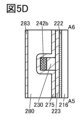
- Fig. 5A is a plan view showing an example of a semiconductor device
- Figs. 5B to 5D are cross-sectional views showing an example of the semiconductor device.
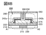
- Fig. 6A is a plan view showing an example of a semiconductor device
- Figs. 6B to 6D are cross-sectional views showing an example of the semiconductor device
- Fig. 7A is a plan view showing an example of a semiconductor device
- Figs. 7B to 7D are cross-sectional views showing an example of the semiconductor device
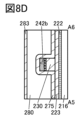
- Fig. 8A is a plan view showing an example of a semiconductor device
- Figs. 8B to 8D are cross-sectional views showing an example of the semiconductor device.
- 9A is a plan view showing an example of a semiconductor device
- FIGS. 9B to 9D are cross-sectional views showing an example of the semiconductor device
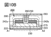
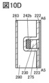
- Fig. 10A is a plan view showing an example of a semiconductor device, and Figs.
- FIG. 10B to 10D are cross-sectional views showing an example of the semiconductor device.
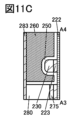
- Fig. 11A is a plan view showing an example of a semiconductor device, and Figs. 11B to 11D are cross-sectional views showing an example of the semiconductor device.
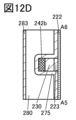
- Fig. 12A is a plan view showing an example of a semiconductor device, and Figs. 12B to 12D are cross-sectional views showing an example of the semiconductor device.
- Fig. 13A is a plan view showing an example of a semiconductor device, and Figs. 13B to 13D are cross-sectional views showing an example of the semiconductor device.
- Fig. 14A is a plan view showing an example of a semiconductor device, Fig. 14B to Fig.
- FIG. 14D are cross-sectional views showing an example of a semiconductor device
- Fig. 14E is a schematic perspective view showing an example of a semiconductor device
- FIG. 15 is a cross-sectional view showing an example of a semiconductor device.
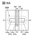
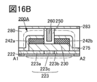
- Fig. 16A is a plan view showing an example of a semiconductor device
- Figs. 16B to 16D are cross-sectional views showing an example of the semiconductor device.
- Fig. 17A is a plan view showing an example of a semiconductor device
- Figs. 17B to 17D are cross-sectional views showing an example of the semiconductor device.
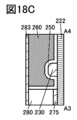
- Fig. 18A is a plan view showing an example of a semiconductor device
- Figs. 18B to 18D are cross-sectional views showing an example of the semiconductor device.
- Fig. 18A is a plan view showing an example of a semiconductor device
- Figs. 18B to 18D are cross-sectional views showing an example of the semiconductor device.
- Fig. 18A is a plan view showing
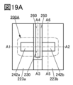
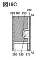
- FIG. 19A is a plan view showing an example of a semiconductor device
- Figs. 19B to 19D are cross-sectional views showing an example of the semiconductor device
- Fig. 20A is a plan view showing an example of a semiconductor device
- Fig. 20B to Fig. 20D are cross-sectional views showing an example of the semiconductor device
- Fig. 21A is a plan view showing an example of a semiconductor device
- Fig. 21B to Fig. 21D are cross-sectional views showing an example of the semiconductor device
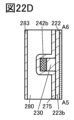
- Fig. 22A is a plan view showing an example of a semiconductor device
- Fig. 22B to Fig. 22D are cross-sectional views showing an example of the semiconductor device.
- Fig. 22A is a plan view showing an example of a semiconductor device
- Fig. 22B to Fig. 22D are cross-sectional views showing an example of the semiconductor device.
- Fig. 22A is a plan view showing an example of a semiconductor device
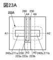
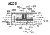
- FIG. 23A is a plan view showing an example of a semiconductor device
- Fig. 23B to Fig. 23D are cross-sectional views showing an example of the semiconductor device
- Fig. 24A is a plan view showing an example of a semiconductor device
- Fig. 24B to Fig. 24D are cross-sectional views showing an example of the semiconductor device
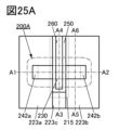
- Fig. 25A is a plan view showing an example of a semiconductor device
- Fig. 25B to Fig. 25D are cross-sectional views showing an example of the semiconductor device
- Fig. 26A is a plan view showing an example of a semiconductor device
- Fig. 26B to Fig. 26D are cross-sectional views showing an example of the semiconductor device.
- Fig. 26A is a plan view showing an example of a semiconductor device
- Fig. 26B to Fig. 26D are cross-sectional views showing an example of the semiconductor device.
- Fig. 26A is a plan view showing an example of a semiconductor device
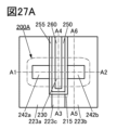
- FIG. 27A is a plan view showing an example of a semiconductor device
- Fig. 27B to Fig. 27D are cross-sectional views showing an example of the semiconductor device
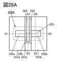
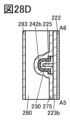
- Fig. 28A is a plan view showing an example of a semiconductor device
- Fig. 28B to Fig. 28D are cross-sectional views showing an example of the semiconductor device
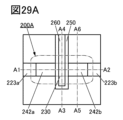
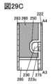
- Fig. 29A is a plan view showing an example of a semiconductor device
- Fig. 29B to Fig. 29D are cross-sectional views showing an example of the semiconductor device
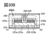
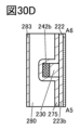
- Fig. 30A is a plan view showing an example of a semiconductor device
- Fig. 30B to Fig. 30D are cross-sectional views showing an example of the semiconductor device.
- Fig. 30A is a plan view showing an example of a semiconductor device
- Fig. 30B to Fig. 30D are cross-sectional views showing an example of the semiconductor device.
- Fig. 30A is a plan view showing an example of a semiconductor device
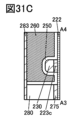
- FIG. 31A is a plan view showing an example of a semiconductor device
- Fig. 31B to Fig. 31D are cross-sectional views showing an example of the semiconductor device
- Fig. 32A is a plan view showing an example of a semiconductor device
- Fig. 32B to Fig. 32D are cross-sectional views showing an example of the semiconductor device
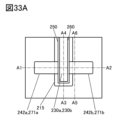
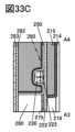
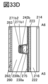
- Fig. 33A is a plan view showing an example of a semiconductor device
- Fig. 33B to Fig. 33D are cross-sectional views showing an example of the semiconductor device
- 34A and 34B are cross-sectional views showing an example of a semiconductor device
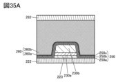
- 35A and 35B are cross-sectional views showing an example of a semiconductor device.
- Fig. 31B to Fig. 31D are cross-sectional views showing an example of the semiconductor device.
- Fig. 32A is a plan view showing an example of a semiconductor device
- Fig. 32B to Fig. 32D are cross-sectional views showing an example of the semiconductor device
- FIG. 36A is a plan view showing an example of a semiconductor device
- Fig. 36B to Fig. 36D are cross-sectional views showing an example of the semiconductor device
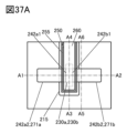
- Fig. 37A is a plan view showing an example of a semiconductor device
- Fig. 37B to Fig. 37D are cross-sectional views showing an example of the semiconductor device
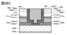
- 38A to 38C are cross-sectional views showing an example of a semiconductor device
- 39A to 39C are cross-sectional views showing an example of a semiconductor device
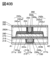
- Fig. 40A is a plan view showing an example of a semiconductor device
- Fig. 40B to Fig. 40D are cross-sectional views showing an example of the semiconductor device.
- Fig. 40A is a plan view showing an example of a semiconductor device
- Fig. 40B to Fig. 40D are cross-sectional views showing an example of the semiconductor device.
- Fig. 40A is a plan view showing an example of a semiconductor device
- FIG. 41A is a plan view showing an example of a semiconductor device
- Fig. 41B to Fig. 41D are cross-sectional views showing an example of the semiconductor device.
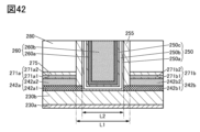
- FIG. 42 is a cross-sectional view showing an example of a semiconductor device.
- 43A to 43D are cross-sectional views showing an example of a semiconductor device.
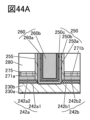
- 44A to 44C are cross-sectional views showing an example of a semiconductor device.
- Fig. 45A is a plan view showing an example of a semiconductor device, and Fig. 45B to Fig. 45D are cross-sectional views showing an example of the semiconductor device.
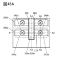
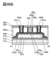
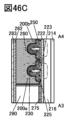
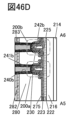
- Fig. 46A is a plan view showing an example of a semiconductor device
- Fig. 46B to Fig. 46D are cross-sectional views showing an example of the semiconductor device.
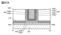
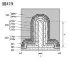
- FIG. 47A and 47B are cross-sectional views showing an example of a semiconductor device.
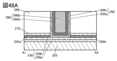
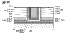
- 48A to 48C are cross-sectional views showing an example of a semiconductor device.
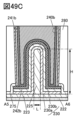
- 49A to 49C are cross-sectional views showing an example of a semiconductor device.
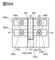
- Fig. 50A is a plan view showing an example of a semiconductor device
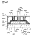
- Fig. 50B to Fig. 50D are cross-sectional views showing an example of the semiconductor device.
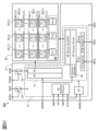
- FIG. 51 is a block diagram showing an example of a storage device.
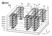
- 52A and 52B are a schematic diagram and a circuit diagram showing an example of a memory device.
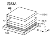
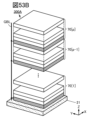
- 53A and 53B are schematic diagrams showing an example of a storage device.
- FIG. 54 is a circuit diagram showing an example of a memory device.
- 55A and 55B are cross-sectional views showing an example of a memory device.
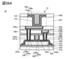
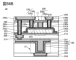
- 56A and 56B are cross-sectional views showing an example of a memory device.
- FIG. 57 is a cross-sectional view showing an example of a memory device.
- 58A and 58B are diagrams showing an example of a semiconductor device.
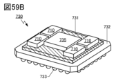
- 59A and 59B are diagrams showing an example of an electronic component.
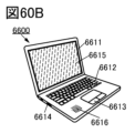
- 60A and 60B are diagrams showing an example of an electronic device, and
- FIGS. 60C to 60E are diagrams showing an example of a mainframe computer.
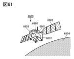
- FIG. 61 is a diagram showing an example of space equipment.
- FIG. 62 is a diagram illustrating an example of a storage system applicable to a data center.
- FIG. 63 is a diagram for explaining the laminated structure of the laminated film.
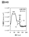
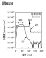
- 64A and 64B show the results of SIMS analysis of the prepared sample.
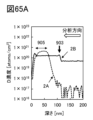
- 65A to 65C show the results of SIMS analysis of the prepared sample.
- top views also called “top views”
- perspective views some components may be omitted from the illustration. Also, some hidden lines may be omitted from the illustration.
- ordinal numbers “first” and “second” are used for convenience and do not limit the number of components or the order of the components (e.g., the order of processes or the order of stacking). Furthermore, an ordinal number attached to a component in one place in this specification may not match an ordinal number attached to the same component in another place in this specification or in the claims.
- film and “layer” may be interchangeable depending on the circumstances.
- conductive layer may be interchangeable with the term “conductive film”.
- insulating film may be interchangeable with the term “insulating layer”.
- conductor may be interchangeable with the term “conductive layer” or the term “conductive film” depending on the circumstances.
- insulating material may be interchangeable with the term “insulating layer” or the term “insulating film” depending on the circumstances.
- parallel refers to a state in which two straight lines are arranged at an angle of -10 degrees or more and 10 degrees or less. Therefore, it also includes cases where the angle is -5 degrees or more and 5 degrees or less.
- approximately parallel refers to a state in which two straight lines are arranged at an angle of -30 degrees or more and 30 degrees or less.
- Perfect refers to a state in which two straight lines are arranged at an angle of 80 degrees or more and 100 degrees or less. Therefore, it also includes cases where the angle is 85 degrees or more and 95 degrees or less.
- approximately perpendicular refers to a state in which two straight lines are arranged at an angle of 60 degrees or more and 120 degrees or less.
- Openings include, for example, grooves and slits. Also, the area in which an opening is formed may be referred to as an opening.
- the sidewalls of the insulator at the opening in the insulator are shown as being perpendicular or approximately perpendicular to the substrate surface or the surface on which the insulator is formed, but they may also be tapered.
- a tapered shape refers to a shape in which at least a portion of the side of the structure is inclined with respect to the substrate surface or the surface on which the structure is to be formed.
- the taper angle there is a region in which the angle between the inclined side and the substrate surface or the surface on which the structure is to be formed (hereinafter, sometimes referred to as the taper angle) is less than 90°.
- the side of the structure and the substrate surface do not necessarily need to be completely flat, and may be approximately planar with a slight curvature, or approximately planar with fine irregularities.
- “same height” refers to a configuration in which the heights from a reference surface (for example, a flat surface such as a substrate surface) are equal in cross-sectional view.
- a planarization process typically a CMP process
- the surfaces treated in the CMP process have a configuration in which the heights from the reference surface are equal.
- the heights of multiple layers may differ depending on the processing device, processing method, or material of the surface treated in the CMP process. In this specification, this case is also treated as "same height”.
- first layer and a second layer when there are two layers (here, a first layer and a second layer) with different heights relative to the reference surface, and the difference in height between the top surface of the first layer and the top surface of the second layer is 20 nm or less, this is also referred to as "same height”.
- side edges coincide means that at least a portion of the contours of the stacked layers overlap when viewed in a plane. For example, this includes cases where the upper and lower layers are processed using the same mask pattern, or where a portion of the mask pattern is the same. However, strictly speaking, the contours may not overlap, and the contour of the upper layer may be located inside the contour of the lower layer, or the contour of the upper layer may be located outside the contour of the lower layer, in which case it is also referred to as "side edges coincide”.
- the first film thickness and the second film thickness being the same means that the absolute value of the difference between the first film thickness and the second film thickness divided by the first film thickness is 0.1 or less. Alternatively, it means that the absolute value of the difference between the first film thickness and the second film thickness divided by the second film thickness is 0.1 or less.
- distance A and distance B are the same means that the absolute value of the difference between distance A and distance B divided by distance A is 0.1 or less. Or, the absolute value of the difference between distance A and distance B divided by distance B is 0.1 or less.
- the semiconductor device according to one embodiment of the present invention includes a transistor.
- a in each figure shows a plan view of the semiconductor device.
- B in each figure is a cross-sectional view corresponding to the portion indicated by the dashed line A1-A2 in A of each figure, and is also a cross-sectional view in the channel length direction of the transistor.
- C in each figure is a cross-sectional view corresponding to the portion indicated by the dashed line A3-A4 in A of each figure, and is also a cross-sectional view in the channel width direction of the transistor.
- D in each figure is a cross-sectional view corresponding to the portion indicated by the dashed line A5-A6 in A of each figure. In the plan view of A in each figure, some elements are omitted to clarify the figure.
- 1A to 1D are plan views and cross-sectional views of a semiconductor device including a transistor 200.
- the semiconductor device shown in Figures 1A to 1D has an insulator 222 on a substrate (not shown), a transistor 200 on the insulator 222, an insulator 280 on the transistor 200, and an insulator 283 on the insulator 280.
- the insulators 222, 280, and 283 function as interlayer insulating films.
- the transistor 200 has an insulator 223 on the insulator 222, an oxide semiconductor 230 on the insulator 223, a conductor 242a and a conductor 242b on the oxide semiconductor 230, an insulator 275 on the insulator 223, the conductor 242a, and the conductor 242b, an insulator 250 on the oxide semiconductor 230, and a conductor 260 located on the insulator 250 and overlapping with a portion of the oxide semiconductor 230.
- the conductor 260 functions as a gate electrode of the transistor 200.
- the insulator 250 functions as a gate insulator of the transistor 200.
- the conductor 242a functions as one of the source electrode and drain electrode of the transistor 200, and the conductor 242b functions as the other of the source electrode and drain electrode of the transistor 200.
- At least a part of the region of the oxide semiconductor 230 that overlaps with the conductor 260 functions as a channel formation region of the transistor 200.
- FIG. 1E shows a schematic perspective view of the semiconductor device.
- insulator 222, insulator 223, oxide semiconductor 230, conductor 242b, insulator 250, conductor 260, insulator 275, and a portion of the surrounding area are shown cut away.
- FIG. 1E only the outlines of some components (e.g., insulator 280 and insulator 283) are shown by dashed lines.
- the oxide semiconductor 230 is provided in contact with the upper surface of the insulator 223.
- the conductor 242a and the conductor 242b are provided in contact with the upper surface of the oxide semiconductor 230.
- the insulator 275 is disposed on the insulator 223, the oxide semiconductor 230, the conductor 242a, and the conductor 242b. Specifically, the insulator 275 is provided in contact with the upper surface of the insulator 223, the side surface of the oxide semiconductor 230, the upper surface and side surface of the conductor 242a, and the upper surface and side surface of the conductor 242b.
- Insulator 280 is provided in contact with the upper surface of insulator 275.
- Each of the insulators 280 and 275 has an opening that reaches the oxide semiconductor 230.
- the insulator 223 also has an opening in a region of the opening that does not overlap with the oxide semiconductor 230.
- the opening in the insulator 280 is referred to as a first opening
- the opening in the insulator 275 is referred to as a second opening
- the opening in the insulator 223 is referred to as a third opening.
- the first opening, the second opening, and the third opening are collectively referred to as opening 290.
- the insulator 250 and the conductor 260 are provided inside the opening 290. That is, at least a portion of each of the insulator 250 and the conductor 260 is provided inside the first opening, the second opening, and the third opening. In addition, the insulator 250 and the conductor 260 are provided between the conductor 242a and the conductor 242b in the channel length direction of the transistor 200.
- Insulator 250 contacts the side of insulator 280 and the side of insulator 275 at opening 290. In addition, insulator 250 contacts the side of conductor 242a facing conductor 260 and the side of conductor 242b facing conductor 260. As shown in FIG. 1C, insulator 250 contacts the top and side of oxide semiconductor 230, the side of insulator 223, and the top of insulator 222 at opening 290.
- the conductor 260 is formed in a self-aligned manner so as to fill the opening 290.
- the conductor 260 can be reliably positioned in the region between the conductor 242a and the conductor 242b without alignment.
- the height of the upper surface of the conductor 260 coincides with the height of the insulator 250 and the insulator 280.
- the sidewall of the opening 290 is perpendicular or approximately perpendicular to the surface on which the oxide semiconductor 230 is to be formed, but this is not limited to this embodiment.
- the bottom surface of the opening 290 may be U-shaped with a gentle curve.
- the sidewall of the opening 290 may be tapered.
- the sidewall of the opening 290 corresponds to the side surface of the insulator 280 in the opening 290, the side surface of the insulator 275 in the opening 290, and the side surface of the insulator 223 in the opening 290.
- Insulator 283 is disposed on insulator 280, on insulator 250, and on conductor 260.
- the transistor 200 preferably uses a metal oxide (hereinafter also referred to as an oxide semiconductor) that functions as a semiconductor for the oxide semiconductor 230 including the channel formation region.
- a metal oxide described in the [Metal Oxide] section described later can be used in a single layer or a stacked layer.
- the composition close thereto includes a range of ⁇ 30% of the desired atomic ratio. It is also preferable to use gallium as the element M.
- the oxide semiconductor 230 may not contain the element M.
- the metal oxide used as the oxide semiconductor 230 may be an In-Zn oxide.
- the composition of the metal oxide used in the oxide semiconductor 230 can be analyzed using, for example, energy dispersive X-ray spectroscopy (EDX), X-ray photoelectron spectroscopy (XPS), inductively coupled plasma mass spectrometry (ICP-MS), or inductively coupled plasma-atomic emission spectrometry (ICP-AES).
- EDX energy dispersive X-ray spectroscopy
- XPS X-ray photoelectron spectroscopy
- ICP-MS inductively coupled plasma mass spectrometry
- ICP-AES inductively coupled plasma-atomic emission spectrometry
- a combination of these techniques may be used for the analysis.
- the actual content may differ from the content obtained by analysis due to the influence of analytical accuracy. For example, if the content of element M is low, the content of element M obtained by analysis may be lower than the actual content.
- the metal oxide can be formed preferably by sputtering or atomic layer deposition (ALD).
- ALD atomic layer deposition
- the composition of the formed metal oxide may differ from the composition of the sputtering target.
- the zinc content in the formed metal oxide may decrease to about 50% compared to the sputtering target.
- Examples of the ALD method include the Thermal ALD method, in which the reaction between the precursor and reactant is carried out using only thermal energy, and the Plasma Enhanced ALD (PEALD) method, in which a plasma-excited reactant is used.
- Thermal ALD method in which the reaction between the precursor and reactant is carried out using only thermal energy
- PEALD Plasma Enhanced ALD
- the ALD method can deposit atoms one layer at a time, which has the following advantages: extremely thin films can be formed; films can be formed on structures with high aspect ratios or surfaces with large steps; films can be formed with few defects such as pinholes; films can be formed with excellent coverage; and films can be formed at low temperatures.
- the PEALD method may be preferable in some cases because it uses plasma, which allows films to be formed at lower temperatures.
- some precursors used in the ALD method contain elements such as carbon or chlorine.
- films formed by the ALD method may contain more elements such as carbon or chlorine than films formed by other film formation methods. Note that the amount of these elements can be quantified using XPS or secondary ion mass spectrometry (SIMS).
- the metal oxide film formation method uses the ALD method, but because it employs a high substrate temperature condition during film formation and/or performs an impurity removal process, the amount of carbon and chlorine contained in the film may be less than when the ALD method is used without applying these conditions.
- the ALD method is a film formation method in which a film is formed by a reaction on the surface of a workpiece, unlike a film formation method in which particles released from a target are deposited. Therefore, it is a film formation method that is not easily affected by the shape of the workpiece and has good step coverage.
- the ALD method has excellent step coverage and excellent thickness uniformity, making it suitable for coating the surface of an opening with a high aspect ratio.
- the ALD method since the ALD method has a relatively slow film formation speed, it may be preferable to use it in combination with other film formation methods such as a sputtering method or a CVD method, which have a fast film formation speed.
- the metal oxide has a layered structure of a first metal oxide and a second metal oxide
- a method of forming a film of the first metal oxide using a sputtering method and forming a film of the second metal oxide on the first metal oxide using an ALD method can be mentioned.
- the first metal oxide has a crystalline portion
- the second metal oxide may grow as a crystal using the crystalline portion as a nucleus.
- the ALD method can control the composition of the resulting film by adjusting the amount of raw material gas introduced.
- the ALD method can form a film of any composition by adjusting the amount of raw material gas introduced, the number of times it is introduced (also called the number of pulses), the time required for one pulse (also called the pulse time), and the like.
- the ALD method can form a film whose composition changes continuously by changing the raw material gas while forming the film.
- the time required for film formation can be shortened compared to forming a film using multiple film formation chambers because no time is required for transportation and pressure adjustment. Therefore, it may be possible to increase the productivity of memory devices.
- FIG. 2A shows an enlarged view of the channel formation region and its vicinity in FIG. 1B
- FIG. 2B shows an enlarged view of the channel formation region and its vicinity in FIG. 1C
- the oxide semiconductor 230 has a region 231a that overlaps with the conductor 242a, a region 231b that overlaps with the conductor 242b, and a region 231c located between the regions 231a and 231b.
- the oxide semiconductor 230 has the region 231c, and the regions 231a and 231b that are provided so as to sandwich the region 231c.
- Region 231c at least partially overlaps with conductor 260.
- Region 231c also has an area that overlaps with opening 290.
- region 231c has an area that overlaps with a first opening provided in insulator 280 and a second opening provided in insulator 275.
- insulator 280 has a first opening in the area that overlaps with region 231c
- insulator 275 has a second opening in the area that overlaps with region 231c.
- Region 231c functions as a channel formation region of transistor 200.
- Region 231a functions as one of the source region and drain region of transistor 200, and region 231b functions as the other of the source region and drain region of transistor 200.
- the channel formation region of the transistor is a high-resistance region with a low carrier concentration. Therefore, the channel formation region of the transistor can be said to be i-type (intrinsic) or substantially i-type. Furthermore, the source and drain regions of the transistor are regions with a high carrier concentration and low resistance (low-resistance n-type regions) compared to the channel formation region.
- the electrical characteristics are likely to fluctuate and the reliability may be reduced.
- hydrogen near the oxygen vacancies may form defects in which hydrogen is inserted into the oxygen vacancies (hereinafter, may be referred to as VOH ), and may generate electrons that serve as carriers.
- VOH oxygen vacancies
- the transistor is likely to have normally-on characteristics (characteristics in which a channel exists and a current flows through the transistor even when no voltage is applied to the gate electrode). Therefore, it is preferable that the channel formation region in the oxide semiconductor has fewer oxygen vacancies, fewer VOH , or a lower concentration of impurities such as hydrogen, nitrogen, and metal elements than the source and drain regions.
- the source and drain regions in the oxide semiconductor preferably have more oxygen vacancies, more VOH , or a higher concentration of impurities such as hydrogen, nitrogen, or metal elements than the channel formation region.
- an insulator containing oxygen that is desorbed by heating (hereinafter may be referred to as excess oxygen) is preferably provided near the oxide semiconductor.
- excess oxygen oxygen can be supplied from the insulator to a channel formation region of the oxide semiconductor, and oxygen vacancies and VOH can be reduced.
- the on-state current or the field-effect mobility of the transistor may decrease.
- the amount of oxygen supplied to the source and drain regions varies within the substrate plane, which causes variation in the electrical characteristics of the transistor. In other words, it is preferable to prevent an excessive amount of oxygen from being supplied to the source and drain regions of the oxide semiconductor.
- insulator 250 is in contact with the top surface and side surface of region 231c, and insulator 223 is in contact with the bottom surface of oxide semiconductor 230.
- an insulator that is easily permeable to oxygen may be used as insulator 250.
- oxygen contained in the insulator containing excess oxygen can be supplied to region 231c via insulator 250.
- an example of an insulator provided near insulator 250 is insulator 280.
- an insulator containing excess oxygen is used as the insulator 280, it is preferable to provide a barrier insulator against oxygen between the insulator 280 and the regions 231a and 231b. With such a structure, the amount of oxygen supplied to the source region or drain region of the oxide semiconductor 230 can be reduced.
- an insulator 275 is provided between the insulator 280 and the regions 231a and 231b.
- the insulators 223 and 275 it is preferable to use, for example, silicon nitride, more preferably silicon nitride formed by the ALD method, and even more preferably silicon nitride formed by the PEALD method.
- the insulators 223 and 275 each contain silicon and nitrogen.
- the ALD method has excellent step coverage and excellent thickness uniformity, and is therefore suitable for forming thin films and coating surfaces with high aspect ratios.
- a silicon nitride film is formed by using the PEALD method
- a precursor containing a halogen such as fluorine, chlorine, bromine, iodine, etc.
- a plasma treatment is performed in an atmosphere containing a nitriding agent such as N2 , N2O , NH3 , NO, NO2 , or N2O2 , thereby forming a high-quality silicon nitride film.
- insulator 275 is configured to contact a portion of the upper surface of insulator 223. At this time, regions 231a and 231b are surrounded by insulator 223 and insulator 275, respectively. Furthermore, regions 231a and 231b are in contact with insulator 223 and insulator 275, respectively.
- the insulator 250 is configured to contact the side surface of the insulator 223 and a part of the upper surface of the insulator 222. At this time, the region 231c is surrounded by the insulator 223 and the insulator 250. The region 231c is also in contact with the insulator 223 and the insulator 250.
- a structure surrounded by a first insulator and a second insulator refers to a configuration in which the first insulator is located on at least a portion of the top surface and at least a portion of the side surface of the structure, and the second insulator is located on at least a portion of the bottom surface of the structure. Or, it refers to a configuration in which the first insulator is located on at least a portion of the top surface of the structure, and the second insulator is located on at least a portion of the side surface and at least a portion of the bottom surface of the structure.
- another structure may be provided between the first insulator and the structure.
- another structure may be provided between the second insulator and the structure.
- microwave treatment in an atmosphere containing oxygen with the conductor 242a and the conductor 242b provided on the oxide semiconductor 230.
- microwave processing refers to processing using a device with a power source that generates high-density plasma using microwaves.
- microwaves refer to electromagnetic waves with a frequency of 300 MHz or more and 300 GHz or less.
- Microwave processing can also be called microwave-excited high-density plasma processing.
- oxygen gas By performing microwave processing in an atmosphere containing oxygen, oxygen gas can be turned into plasma using microwaves or high frequency waves such as RF, and the oxygen plasma can be made to act. At this time, microwaves or high frequency waves such as RF can also be irradiated onto the region 231c.
- microwaves or high frequency waves such as RF can also be irradiated onto the region 231c.
- the VOH in the region 231c can be split into oxygen vacancies ( V0 ) and hydrogen (H), the hydrogen can be removed from the region 231c, and the oxygen vacancies can be compensated for with oxygen. Therefore, the hydrogen concentration, oxygen vacancies, and VOH in the region 231c can be reduced, and the carrier concentration can be lowered.
- the effects of microwaves, high frequency waves such as RF, oxygen plasma, and the like are shielded by the conductors 242a and 242b and do not reach the regions 231a and 231b. Furthermore, the effects of oxygen plasma can be reduced by the insulators 275 and 280 provided to cover the oxide semiconductor 230, the conductor 242a, and the conductor 242b. As a result, reduction in VOH and supply of an excessive amount of oxygen are not generated in the regions 231a and 231b during microwave treatment, and thus a decrease in carrier concentration can be prevented.
- the insulating film that becomes the insulator 250 it is preferable to perform microwave treatment in an atmosphere containing oxygen.
- microwave treatment in an atmosphere containing oxygen through the insulator 250 in this manner, oxygen can be efficiently injected into the region 231c.
- the insulator 250 by arranging the insulator 250 so that it is in contact with the side of the conductor 242a, the side of the conductor 242b, and the surface of the region 231c, it is possible to prevent the injection of more oxygen than necessary into the region 231c, and to prevent oxidation of the side of the conductor 242a and the conductor 242b.
- the oxygen injected into region 231c can take various forms, such as oxygen atoms, oxygen molecules, oxygen ions (charged oxygen atoms or oxygen molecules), and oxygen radicals (oxygen atoms, oxygen molecules, or oxygen ions with an unpaired electron).
- the oxygen injected into region 231c may take one or more of the above forms, and is particularly preferably oxygen radicals.
- the film quality of insulator 250 can be improved, thereby improving the reliability of transistor 200.
- oxygen vacancies and VOH can be selectively removed from the region 231c functioning as a channel formation region, making the region 231c i-type or substantially i-type. Furthermore, excessive supply of oxygen to the regions 231a and 231b functioning as source and drain regions can be suppressed, and the state of the n-type regions before the microwave treatment can be maintained. This can suppress fluctuations in the electrical characteristics of the transistor 200, and can suppress variations in the electrical characteristics of the transistor 200 within the substrate surface.
- oxygen can be efficiently supplied to region 231c, and the channel formation region can be made into an i-type region. Furthermore, since the amount of oxygen supplied to regions 231a and 231b is smaller than that to region 231c, it is possible to prevent a decrease in the carrier concentration in the source and drain regions.
- a barrier insulator against hydrogen as described in the [Insulator] section below, for the insulator 223 and the insulator 275.
- Silicon nitride has barrier properties against hydrogen and is therefore suitable for the insulator 275 and the insulator 223.
- Silicon nitride which can be used as insulator 223 and insulator 275, has a barrier property against oxygen if the film thickness is, for example, 1.0 nm or more, and has a high barrier property against oxygen if the film thickness is, for example, 1.4 nm or more. Silicon nitride also has a barrier property against hydrogen if the film thickness is, for example, 2.5 nm or more, and has a high barrier property against hydrogen if the film thickness is, for example, 3.3 nm or more.
- the thickness of the insulator 223 is preferably 1.0 nm or more, and more preferably 1.4 nm or more.
- the upper limit of the thickness of the insulator 223 is not particularly limited, but from the viewpoint of miniaturization or high integration of the semiconductor device and improvement of the productivity of the semiconductor device, it is preferably 20 nm or less, 10 nm or less, or 5.0 nm or less. Therefore, the insulator 223 preferably has a region with a thickness of 1.0 nm or more and 10 nm or less, and more preferably has a region with a thickness of 1.0 nm or more and 5.0 nm or less. Furthermore, the insulator 223 preferably has a region with a thickness of 1.4 nm or more and 10 nm or less, and more preferably has a region with a thickness of 1.4 nm or more and 5.0 nm or less.
- insulator 223 and insulator 275 are formed using the same insulating material, a third opening is formed in insulator 223 when insulator 275 is etched to form the second opening. At this time, insulator 250 contacts insulator 222 at the third opening (see FIG. 1C).
- Insulators that can be used as the insulators 223 and 275 are not limited to silicon nitride.
- silicon nitride aluminum oxide or hafnium oxide may be used.
- each of the insulators 223 and 275 may have a laminated structure.
- the insulator 223 may have a laminated structure of silicon nitride and aluminum oxide on the silicon nitride, and the insulator 275 may have a laminated structure of aluminum oxide and silicon nitride on the aluminum oxide.
- the insulator 223 may have a laminated structure of aluminum oxide and silicon nitride on the aluminum oxide, and the insulator 275 may have a laminated structure of silicon nitride and aluminum oxide on the silicon nitride.
- the oxide semiconductor 230 preferably has crystallinity.
- oxide semiconductors having crystallinity include CAAC-OS (c-axis aligned crystalline oxide semiconductor), nc-OS (nanocrystalline oxide semiconductor), polycrystalline oxide semiconductor, and single-crystalline oxide semiconductor. It is preferable to use CAAC-OS or nc-OS as the oxide semiconductor 230, and it is particularly preferable to use CAAC-OS.
- CAAC-OS is a metal oxide that has a highly crystalline and dense structure and has few impurities and defects (e.g., oxygen vacancies).
- a temperature e.g. 400°C or higher and 600°C or lower
- the CAAC-OS can be made to have a more crystalline and dense structure. In this way, the density of the CAAC-OS can be further increased, thereby further reducing the diffusion of impurities or oxygen in the CAAC-OS.
- the oxide semiconductor 230 Furthermore, by using a crystalline oxide such as CAAC-OS as the oxide semiconductor 230, it is possible to suppress the extraction of oxygen from the oxide semiconductor 230 by the source electrode or the drain electrode. As a result, even when heat treatment is performed, it is possible to suppress the extraction of oxygen from the oxide semiconductor 230, and therefore the transistor 200 is stable against high temperatures (so-called thermal budget) in the manufacturing process.
- a crystalline oxide such as CAAC-OS
- FIG. 3A and FIG. 3B enlarged views of the channel formation region and its vicinity in FIG. 1C are shown in FIG. 3A and FIG. 3B.
- the CAAC-OS has multiple crystals, and each of the multiple crystals has a crystal structure in which multiple layers are stacked.
- the c-axis of the crystals of the CAAC-OS used as the oxide semiconductor 230 is preferably oriented in a direction perpendicular to the channel length direction.
- the c-axis of the crystals of the region 231c that functions as a channel formation region is preferably oriented in a direction perpendicular to the channel length direction.
- the channel formation region is electrically surrounded by the electric field of the conductor 260. Therefore, the side surface of region 231c also functions as a channel formation region. Therefore, it is preferable that the c-axis of the crystals in the vicinity of the side surface of region 231c facing the insulator 250 is also oriented in a direction perpendicular to the channel length direction. In other words, it is preferable that region 231c has crystals in the side surface near the insulator 250, and that the c-axis of the crystals is oriented in a direction perpendicular to the channel length direction.
- One example of the above-mentioned structure is a structure in which a layer contained in the crystal extends parallel or approximately parallel to the surface on which the oxide semiconductor 230 is formed (see FIG. 3A).
- the above-mentioned crystals are formed during the formation of the oxide semiconductor film that becomes the oxide semiconductor 230, so that the oxide semiconductor 230 having the crystals can be formed.
- the oxide semiconductor film is preferably formed while heating the substrate. Note that an oxide semiconductor film formed by a sputtering method is likely to have crystallinity, and is therefore suitable for forming the oxide semiconductor 230 having the crystals.
- the oxide semiconductor 230 having the above-mentioned crystals can be formed by processing the oxide semiconductor film to be the oxide semiconductor 230 into an island shape and then performing a process selected from plasma processing, microwave processing, and heat treatment, for example, to form the oxide semiconductor 230 into a crystal structure.
- the oxide semiconductor film is formed by the ALD method, the crystallinity of the oxide semiconductor film may be low due to remaining impurities contained in the raw material such as a precursor. Therefore, by forming the oxide semiconductor film, processing it into an island shape, and then performing the above process, the impurity concentration of the oxide semiconductor 230 can be reduced, and crystal growth from the surface side of the oxide semiconductor 230 can be promoted.
- the method for forming the oxide semiconductor film that becomes the oxide semiconductor 230 is not particularly limited.
- the oxide semiconductor film can be formed using a CVD method, an MBE method, a PLD method, or the like.
- the ALD method may be used to form the structure shown in FIG. 3A, or the sputtering method may be used to form the structure shown in FIG. 3B.
- the crystallinity of the oxide semiconductor 230 can be analyzed, for example, by X-ray diffraction (XRD), a transmission electron microscope (TEM), or electron diffraction (ED). Alternatively, the analysis may be performed by combining a plurality of these techniques.
- XRD X-ray diffraction
- TEM transmission electron microscope
- ED electron diffraction
- the oxide semiconductor 230 is shown as a single layer, but the present invention is not limited to this.
- the oxide semiconductor 230 may have a laminated structure of multiple oxide layers with different chemical compositions.
- the oxide semiconductor 230 may have a structure in which multiple types of metal oxides selected from the metal oxides described above and those described in the [Metal Oxide] section below are appropriately laminated.
- the oxide semiconductor 230 may have a stacked structure of an oxide semiconductor 230a, an oxide semiconductor 230b on the oxide semiconductor 230a, and an oxide semiconductor 230c on the oxide semiconductor 230b.
- the atomic ratio of element M to In is preferably greater than the atomic ratio of element M to In in the metal oxide used for oxide semiconductor 230b.
- the insulator 223 may not be effective in suppressing the diffusion of hydrogen.
- the oxide semiconductor 230a between the insulator 223 and the oxide semiconductor 230b the diffusion of hydrogen from the substrate side to the oxide semiconductor 230b can be suppressed.
- the oxide semiconductor 230a may not be provided.
- the oxide semiconductor 230 may have a stacked structure of an oxide semiconductor 230b and an oxide semiconductor 230c on the oxide semiconductor 230b.
- the thickness of the insulator 223 is not limited to the above. Even if the thickness of the insulator 223 is 1.0 nm or more or 1.4 nm or more and 2.5 nm or less, the oxide semiconductor 230a may not be provided.
- the oxide semiconductor 230a may not be provided.
- the oxide semiconductor film that becomes the oxide semiconductor 230b is formed using an ALD method or a CVD method
- the oxide semiconductor 230a may not be provided.
- damage to the insulator 223 is reduced, and the diffusion of elements contained in the insulator 223 into the oxide semiconductor film can be suppressed.
- the conductivity of the material used for the oxide semiconductor 230b may differ from the conductivity of the material used for the oxide semiconductor 230a.
- the band gap of the material used for the oxide semiconductor 230b may differ from the band gap of the material used for the oxide semiconductor 230a.
- the conductivity of the material used for the oxide semiconductor 230b is preferably different from that of the material used for the oxide semiconductor 230c.
- a material having a higher conductivity than the oxide semiconductor 230c can be used for the oxide semiconductor 230b.
- a transistor with a large on-state current can be obtained.
- the oxide semiconductor 230b may be made of a material having a higher conductivity than the oxide semiconductor 230a. By using a material having a high conductivity for the oxide semiconductor 230b, a transistor having a large on-state current can be obtained.
- the atomic ratio of In to Zn in the oxide semiconductor 230b is preferably greater than the atomic ratio of In to Zn in the oxide semiconductor 230a.
- the atomic ratio of In to Zn in the oxide semiconductor 230b is preferably greater than the atomic ratio of In to Zn in the oxide semiconductor 230c.
- the film thickness of the oxide semiconductor 230b is preferably greater than the film thickness of the oxide semiconductor 230a and the film thickness of the oxide semiconductor 230c.
- the threshold voltage of the transistor 200 may shift, and the drain current (hereinafter also referred to as cutoff current) that flows when the gate voltage is 0 V may become large.
- the threshold voltage may become low. Therefore, it is preferable to use a material with lower conductivity than the oxide semiconductor 230b for the oxide semiconductor 230c.
- the threshold voltage can be increased, and the transistor can have a small cutoff current. Note that a small cutoff current may be referred to as a normally-off transistor.
- the oxide semiconductor 230b As described above, by using a material having a higher conductivity than the oxide semiconductor 230c as the oxide semiconductor 230b, a normally-off transistor with a large on-state current can be obtained. Therefore, a semiconductor device that achieves both low power consumption and high performance can be obtained.
- the carrier concentration of the oxide semiconductor 230b is preferably higher than that of the oxide semiconductor 230c.
- the conductivity is increased, and a transistor with a large on-state current can be obtained.
- the conductivity is decreased, and a normally-off transistor can be obtained.
- the oxide semiconductor 230b is made of a material having a higher conductivity than the oxide semiconductor 230c; however, one embodiment of the present invention is not limited to this.
- the oxide semiconductor 230b may be made of a material having a lower conductivity than the oxide semiconductor 230c.
- the carrier concentration of the oxide semiconductor 230b may be lower than the carrier concentration of the oxide semiconductor 230c.
- the band gap of the first metal oxide used in the oxide semiconductor 230b is preferably different from the band gap of the second metal oxide used in the oxide semiconductor 230c.
- the difference between the band gap of the first metal oxide and the band gap of the second metal oxide is preferably 0.1 eV or more, more preferably 0.2 eV or more, and even more preferably 0.3 eV or more.
- the band gap of the first metal oxide used in the oxide semiconductor 230b can be smaller than the band gap of the second metal oxide used in the oxide semiconductor 230c. With this configuration, a transistor with a large on-state current can be obtained. Furthermore, when the transistor 200 is an n-channel transistor, the threshold voltage can be increased, and the transistor can be a normally-off transistor.
- the band gap of the first metal oxide is smaller than the band gap of the second metal oxide, but one embodiment of the present invention is not limited to this.
- the band gap of the first metal oxide may be larger than the band gap of the second metal oxide.
- the oxide semiconductor 230c has a higher barrier property against oxygen than the oxide semiconductor 230b.
- the oxide semiconductor 230c By disposing the oxide semiconductor 230c between the conductor 242a and the oxide semiconductor 230b and between the conductor 242b and the oxide semiconductor 230b, it is possible to suppress the conductor 242a and the conductor 242b from being oxidized by the oxygen contained in the oxide semiconductor 230b, which would increase the resistivity and reduce the on-current. Therefore, it is possible to improve the electrical characteristics, field effect mobility, and reliability of the transistor 200.
- the oxide semiconductor 230c may not be provided.
- the oxide semiconductor 230 may have a stacked structure of the oxide semiconductor 230a and the oxide semiconductor 230b on the oxide semiconductor 230a.
- the insulators described in the section [Insulators] below can be used in a single layer or a multilayer.
- silicon oxide or silicon oxynitride can be used as the insulator 250. Silicon oxide and silicon oxynitride are preferred because they are stable against heat.
- insulator 250 a material with a high relative dielectric constant, so-called high-k material, described in the section [Insulator] below, may be used.
- high-k material a material with a high relative dielectric constant
- hafnium oxide or aluminum oxide may be used.
- the insulator 250 is provided in an opening formed in the insulator 280, etc., together with the conductor 260. In order to miniaturize the transistor 200, it is preferable that the thickness of the insulator 250 is thin.
- the thickness of the insulator 250 is preferably 0.5 nm or more and 15 nm or less, more preferably 0.5 nm or more and 12 nm or less, and even more preferably 0.5 nm or more and 10 nm or less. It is sufficient that at least a part of the insulator 250 has a region with the above-mentioned thickness.
- the concentration of impurities such as water and hydrogen in the insulator 250 is reduced. This can prevent impurities such as water and hydrogen from entering the channel formation region of the oxide semiconductor 230.
- Insulator 250 may have a laminated structure.
- insulator 250 may have a laminated structure of insulator 250a, insulator 250b on insulator 250a, and insulator 250c on insulator 250b.
- insulator 250b it is advisable to use an insulator that is applicable to insulator 250 described above.
- the insulator 250a is preferably an oxygen barrier insulator as described in the [Insulator] section below.
- the insulator 250a has a region in contact with the oxide semiconductor 230.
- the insulator 250a has a barrier property against oxygen, and thus can suppress oxygen from being released from the oxide semiconductor 230 when heat treatment or the like is performed. This can suppress the formation of oxygen vacancies in the oxide semiconductor 230. This can improve the electrical characteristics and reliability of the transistor 200.
- aluminum oxide can be used as the insulator 250a. In this case, the insulator 250a contains at least oxygen and aluminum.
- the insulator 250c is preferably a barrier insulator against hydrogen, as described in the [Insulator] section below. This can suppress the diffusion of impurities contained in the conductor 260 into the oxide semiconductor 230. Silicon nitride has high hydrogen barrier properties and is therefore suitable as the insulator 250c. In this case, the insulator 250c contains at least nitrogen and silicon.
- the insulator 250c may further have a barrier property against oxygen.
- the insulator 250c is provided between the insulator 250b and the conductor 260. This prevents the oxygen contained in the insulator 250b from diffusing into the conductor 260, and suppresses oxidation of the conductor 260. In addition, a decrease in the amount of oxygen supplied to the region 231c can be suppressed.
- an insulator may be provided between the insulator 250b and the insulator 250c.
- the insulator it is preferable to use an insulator having a function of capturing or fixing hydrogen, as described in the section [Insulator] below.
- the insulator hydrogen contained in the oxide semiconductor 230 can be captured or fixed more effectively.
- the hydrogen concentration in the oxide semiconductor 230 can be reduced.
- hafnium oxide may be used as the insulator.
- the insulator contains at least oxygen and hafnium.
- the insulator may have an amorphous structure.
- the thicknesses of the insulators 250a to 250c are preferably thin and within the aforementioned range.
- the thicknesses of the insulators 250a, 250b, the insulator having the function of capturing or fixing hydrogen, and the insulator 250c are 1 nm, 2 nm, 2 nm, and 1 nm, respectively.
- the films In order to make the film thickness of the insulators 250a to 250c as thin as described above, it is preferable to form the films using the ALD method. Also, in order to provide the insulators 250a to 250c inside the openings provided in the insulator 280, etc., it is preferable to form the films using the ALD method.
- Figures 4A to 4D show a configuration in which the insulator 250 has a three-layer stacked structure of insulators 250a to 250c, the present invention is not limited to this.
- the insulator 250 may have a two-layer or four or more layer stacked structure.
- each layer included in the insulator 250 may be appropriately selected from insulators 250a to 250c and insulators that have the function of capturing or fixing hydrogen.
- the insulator 280 functions as an interlayer film, it is preferable that it has a low dielectric constant. By using a material with a low dielectric constant as the interlayer film, the parasitic capacitance that occurs between wiring can be reduced.
- the insulator 280 a single layer or a multilayer of insulators containing a material with a low dielectric constant, as described in the [Insulator] section below, can be used. Silicon oxide and silicon oxynitride are preferable because they are thermally stable.
- the concentration of impurities such as water and hydrogen in the insulator 280 is reduced. This can suppress the intrusion of impurities such as water and hydrogen into the channel formation region of the oxide semiconductor 230.
- the insulator 283 is preferably a barrier insulator against hydrogen, as described in the [Insulator] section below. This can prevent hydrogen from diffusing from outside the transistor 200 to the oxide semiconductor 230 through the insulator 250. Silicon nitride and silicon nitride oxide each have the characteristics of releasing little impurities (e.g., water and hydrogen) from themselves and being less permeable to oxygen and hydrogen, and therefore can be suitably used for the insulator 283.
- impurities e.g., water and hydrogen
- the insulator 283 contains silicon and nitrogen.
- the sputtering method does not require the use of molecules containing hydrogen in the deposition gas, and therefore the hydrogen concentration in the insulator 283 can be reduced. Furthermore, by depositing the insulator 283 by sputtering, silicon nitride with high density can be formed.
- the film thickness of insulator 223 may be different from the film thickness of insulator 283.
- the film thickness of insulator 223 is smaller than the film thickness of insulator 283.
- Insulator 223 may have at least a portion of a region having a smaller film thickness than insulator 283.
- insulator 223 preferably has barrier properties against at least oxygen, and insulator 283 preferably has barrier properties against hydrogen. Therefore, insulator 223 may have a region having a smaller film thickness than insulator 283.
- the concentration of the impurity element in the insulator 223 may be different from the concentration of the impurity element in the insulator 283.
- the concentration of the impurity element in the insulator 223 may be higher than the concentration of the impurity element in the insulator 283.
- the impurity element is a halogen such as fluorine, chlorine, bromine, or iodine, hydrogen, or carbon.
- the insulator 223 is preferably formed by the ALD method, and the insulator 283 is preferably formed by the sputtering method. When an insulator is formed by the ALD method, impurities contained in the raw materials such as the precursor remain.
- the insulator formed by the ALD method tends to have a high concentration of the impurity element.
- the insulator formed by the ALD method tends to have a high concentration of the halogen.
- the concentration of the halogen in the insulator 223 may be higher than the concentration of the halogen in the insulator 283.
- the insulator formed using the ALD method tends to have high hydrogen and carbon concentrations. That is, the hydrogen concentration of the insulator 223 may be higher than the hydrogen concentration of the insulator 283.
- the carbon concentration of the insulator 223 may be higher than the carbon concentration of the insulator 283.
- the insulator 222 is preferably a barrier insulator against hydrogen, as described in the [Insulator] section below.
- the insulator 222 has a barrier property against hydrogen, the diffusion of hydrogen from below the insulator 222 to the oxide semiconductor 230 can be suppressed even if the thickness of the insulator 223 is thin.
- the insulator 222 is made of a metal oxide having an amorphous structure. With this structure, hydrogen contained in the channel formation region of the transistor 200 can be captured or fixed.
- the insulator 222 may have a barrier property against oxygen.
- the insulator 222 and the insulator 223 that have a barrier property against oxygen it is possible to prevent oxygen from being released from the oxide semiconductor 230.
- an insulator 222 that functions as an etching stopper film when etching insulator 223 to form the third opening.
- the insulator 222 may have a laminated structure.
- the insulator 222 may have a laminated structure of silicon nitride and hafnium oxide on the silicon nitride. With this configuration, it is possible to suppress the diffusion of hydrogen from below the insulator 222 to the oxide semiconductor 230.
- the conductor 260 may be a single layer or a multilayer of the conductors described in the section below titled "Conductor.”
- the conductor 260 may be a highly conductive material such as tungsten.
- the conductor 260 a conductive material that is resistant to oxidation, or a conductive material that has the function of suppressing the diffusion of oxygen.
- conductive materials include conductive materials that contain nitrogen (e.g., titanium nitride or tantalum nitride), and conductive materials that contain oxygen (e.g., ruthenium oxide).
- nitrogen e.g., titanium nitride or tantalum nitride
- oxygen e.g., ruthenium oxide
- the conductor 260 contains at least the metal and nitrogen. This makes it possible to suppress a decrease in the conductivity of the conductor 260.
- the conductor 260 may have a laminated structure.
- the conductor 260 may have a laminated structure of a conductor 260a and a conductor 260b on the conductor 260a.
- the conductor 260a is preferably made of a conductive material that has the function of suppressing the diffusion of oxygen. This can suppress the oxidation of the conductor 260b due to the oxygen contained in the insulator 280, etc., which leads to a decrease in conductivity.
- titanium nitride can be used as the conductor 260a.
- the conductor 260b is preferably made of a conductive material with high conductivity.
- tungsten can be used as the conductor 260b. By providing a layer containing tungsten in this manner, the conductivity of the conductor 260 can be improved, allowing it to function adequately as wiring.
- conductor 260 has a two-layer laminate structure of conductor 260a and conductor 260b
- the present invention is not limited to this.
- Conductor 260 may have a laminate structure of three or more layers.
- conductors 242a and 242b can be used as the conductors 242a and 242b, either in a single layer or in a multilayer configuration.
- the conductors 242a and 242b can be made of a highly conductive material, such as tungsten.
- the conductors 242a and 242b are made of a conductive material that is difficult to oxidize or that has a function of suppressing the diffusion of oxygen.
- a conductive material that is difficult to oxidize or that has a function of suppressing the diffusion of oxygen.
- titanium nitride or tantalum nitride can be used.
- each of the conductors 242a and 242b contains at least a metal and nitrogen. With this configuration, it is possible to suppress excessive oxidation of the conductors 242a and 242b by the oxide semiconductor 230.
- the conductor 242a and the conductor 242b are each shown as a single layer, but the present invention is not limited to this.
- the conductor 242a and the conductor 242b may each have a laminated structure.
- the conductor 242a may have a laminated structure of the conductor 242a1 and the conductor 242a2 on the conductor 242a1.
- the conductor 242b may have a laminated structure of the conductor 242b1 and the conductor 242b2 on the conductor 242b1.
- titanium nitride or tantalum nitride may be used as the conductor 242a1 and the conductor 242b1
- tungsten may be used as the conductor 242a2 and the conductor 242b2.
- insulator 275 is provided so as to contact the upper surface of conductor 242a and the upper surface of conductor 242b, but the present invention is not limited to this.
- insulator 271a may be provided between conductor 242a and insulator 275
- insulator 271b may be provided between conductor 242b and insulator 275.
- Insulator 271a and insulator 271b function as etching stoppers that protect conductor 242a and conductor 242b, respectively. Therefore, as shown in Figures 4B and 4D, in a cross-sectional view of transistor 200, it is preferable that the side end of insulator 271a coincides with the side end of conductor 242a, and the side end of insulator 271b coincides with the side end of conductor 242b.
- Insulators 271a and 271b are in contact with conductors 242a and 242b, respectively, and are therefore preferably inorganic insulators that do not easily oxidize conductors 242a and 242b.
- insulators 271a and 271b it is preferable to use an insulator that is applicable to insulator 275, for example.
- Insulators 271a and 271b are shown as single layers in Figs. 4B and 4D, but the present invention is not limited to this. Insulators 271a and 271b may each have a laminated structure.
- the insulator 283 is provided so as to contact the upper surface of the insulator 280, the upper surface of the insulator 250, and the upper surface of the conductor 260, but the present invention is not limited to this.
- the insulator 282 may be provided between the insulator 283 and the insulators 280, 250, and conductor 260.
- the insulator 282 is preferably an insulator capable of adding oxygen to the insulator 280.
- the insulator 282 contains at least oxygen and aluminum.
- the insulator 282 or an insulating film that becomes the insulator 282 is preferably formed by a sputtering method, and more preferably formed in an oxygen-containing atmosphere by a sputtering method. By forming the insulator 282 in an oxygen-containing atmosphere by a sputtering method, oxygen can be added to the insulator 280 while the insulator 282 is being formed. This allows the insulator 280 to contain excess oxygen.
- a metal oxide having an amorphous structure contains oxygen atoms with dangling bonds, and may have the property of capturing or fixing hydrogen at the dangling bonds.
- a metal oxide having an amorphous structure contains oxygen atoms with dangling bonds, and may have the property of capturing or fixing hydrogen at the dangling bonds.
- the insulator 282 is preferably an amorphous structure, but may have a polycrystalline structure in part.
- the insulator 282 may also have a multi-layer structure in which an amorphous structure layer and a polycrystalline structure layer are stacked.
- the insulator 282 may have a stacked structure in which a polycrystalline structure layer is formed on an amorphous structure layer.
- the insulator 282 is shown as a single layer in Figures 4B to 4D, the present invention is not limited to this.
- the insulator 282 may have a laminated structure.
- [Configuration Example 1-2] 1A to 1D illustrate the case where the transistor 200 has a single-gate structure having one gate, the present invention is not limited to this structure.
- the transistor 200 may have a back gate.
- Figures 5A to 5D are plan views and cross-sectional views of the semiconductor device.
- the semiconductor device shown in Figures 5A to 5D differs from the semiconductor device shown in Figures 1A to 1D mainly in that it has a conductor 215 and an insulator 216.
- FIG. 5A to 5D differs from the semiconductor device shown in Figures 1A to 1D mainly in that it has a conductor 215 and an insulator 216.
- an insulator 216 and a conductor 215 are provided below the insulator 222.
- the conductor 215 is disposed so as to be embedded in an opening formed in the insulator 216.
- the height of the upper surface of the conductor 215 is the same as the height of the upper surface of the insulator 216.
- the conductor 260 functions as a first gate (also called a top gate) electrode
- the conductor 215 functions as a second gate (also called a back gate) electrode
- the insulator 250 functions as a first gate insulator
- a part of the insulator 222 and a part of the insulator 223 function as a second gate insulator. Therefore, it can be said that the transistor 200 further has a conductor 215 and an insulator 222.
- the conductor 215 has an area that overlaps with the conductor 260, sandwiching the insulator 222, the insulator 223, the oxide semiconductor 230, and the insulator 250 therebetween.
- the conductor 215 is preferably larger than the size of the region of the oxide semiconductor 230 that does not overlap with the conductors 242a and 242b. Furthermore, as shown in FIG. 5C, the conductor 215 preferably extends to a region outside the end of the oxide semiconductor 230 in the channel width direction. In other words, the conductor 215 and the conductor 260 preferably overlap with an insulator interposed therebetween on the outside of the side surface of the oxide semiconductor 230 in the channel width direction. With this configuration, the channel formation region of the oxide semiconductor 230 can be electrically surrounded by the electric field of the conductor 260 functioning as the first gate electrode and the electric field of the conductor 215 functioning as the second gate electrode.
- the transistor structure in which the electric field of at least the first gate electrode electrically surrounds the channel formation region is called a surrounded channel (S-channel) structure.
- the S-channel structure disclosed in this specification has a structure different from the Fin type structure and the planar type structure.
- the S-channel structure disclosed in this specification can also be considered as a type of Fin type structure.
- the Fin type structure refers to a structure in which the gate electrode is arranged to surround at least two or more sides of the channel (specifically, two, three, or four sides, etc.).
- the channel formation region can be electrically surrounded.
- the S-channel structure electrically surrounds the channel formation region, and therefore can be said to be substantially equivalent to a GAA (gate all around) structure or a LGAA (lateral gate all around) structure.
- the channel formation region formed at or near the interface between the oxide semiconductor 230 and the gate insulator can be the entire bulk of the oxide semiconductor 230. Therefore, it is possible to improve the density of the current flowing through the transistor, and it is expected to improve the on-current of the transistor or the field effect mobility of the transistor.
- the conductor 215 is extended to function as wiring. However, this is not limited to this, and a conductor that functions as wiring may be provided below the conductor 215. Also, it is not necessary to provide one conductor 215 for each transistor. For example, the conductor 215 may be shared by multiple transistors.
- FIG. 5B shows a configuration in which the conductor 215 is provided as a single layer
- the present invention is not limited to this.
- the conductor 215 may be provided as a laminated structure of two or more layers.
- the conductor 215 may function as a second gate electrode.
- the threshold voltage (Vth) of the transistor 200 can be controlled by changing the potential applied to the conductor 215 independently of the potential applied to the conductor 260.
- applying a negative potential (a potential lower than the source potential) to the conductor 215 can increase the Vth of the transistor 200 and reduce the off-current. Therefore, applying a negative potential to the conductor 215 can reduce the drain current when the potential applied to the conductor 260 is 0 V, compared to not applying a negative potential.
- the electrical resistivity of the conductor 215 is designed taking into consideration the potential applied to the conductor 215, and the film thickness of the conductor 215 is set to match the electrical resistivity.
- the film thickness of the insulator 216 is approximately the same as that of the conductor 215.
- the insulator 216 functions as an interlayer film, it is preferable that it has a low dielectric constant. By using a material with a low dielectric constant as the interlayer film, the parasitic capacitance that occurs between wirings can be reduced.
- the insulator 216 a single layer or a multilayer of insulators containing a material with a low dielectric constant, as described in the [Insulator] section below, can be used. Silicon oxide and silicon oxynitride are preferable because they are thermally stable.
- the concentration of impurities such as water and hydrogen in the insulator 216 is reduced. This can suppress the intrusion of impurities such as water and hydrogen into the channel formation region of the oxide semiconductor 230.
- the side end of the conductor 242a coincides with the side end of the oxide semiconductor 230
- the side end of the conductor 242b coincides with the side end of the oxide semiconductor 230
- the present invention is not limited to this structure.
- the conductor 242a and the conductor 242b may have a region in contact with the side surface of the oxide semiconductor 230.
- Figures 6A to 6D are plan views and cross-sectional views of a semiconductor device having a transistor 200.
- the transistor 200 shown in Figures 6A to 6D differs from the transistor 200 shown in Figures 5A to 5D mainly in the shapes of the conductors 242a and 242b.
- differences from the above-described [Configuration Example 1-1] and [Configuration Example 1-2] will be mainly described, and overlapping parts will be referred to and may not be described.
- the conductor 242a has a region in contact with the upper surface of the insulator 223 and the side surface on the A1 side of the oxide semiconductor 230.
- the conductor 242b has a region in contact with the upper surface of the insulator 223 and the side surface on the A2 side of the oxide semiconductor 230.
- the conductor 242a may have a region that extends in the channel length direction or the channel width direction of the transistor 200. In this case, the conductor 242a can also function as wiring. The same applies to the conductor 242b.
- insulator 250 contacts the side surface of insulator 280, the side surface of insulator 275, and the side surface of insulator 223 in opening 290, but the present invention is not limited to this configuration.
- insulators may be provided between insulator 250 and insulator 280, insulator 275, and insulator 223.
- Figures 7A to 7D are plan views and cross-sectional views of a semiconductor device having a transistor 200.
- the transistor 200 shown in Figures 7A to 7D differs from the transistor 200 shown in Figures 5A to 5D mainly in that it has an insulator 255.
- Figures 7A to 7D show a configuration in which the conductor 242a and the conductor 242b each have a two-layer stacked structure.
- the conductor 242a has a conductor 242a1 and a conductor 242a2 on the conductor 242a1, and the conductor 242b has a conductor 242b1 and a conductor 242b2 on the conductor 242b1.
- Insulator 255 is provided between insulator 250 and insulators 280, 275, and 223. Specifically, in opening 290, insulator 250 contacts the side of insulator 280, the side of insulator 250, the side of conductor 242a2, the top surface of conductor 242a1, the side of conductor 242b2, the top surface of conductor 242b1, the side of insulator 223, and the top surface of insulator 222. In addition, insulator 255 has an opening in the region between conductor 242a1 and conductor 242b1. Hereinafter, the opening provided in insulator 255 is referred to as the fourth opening.
- the distance between conductor 242a1 and conductor 242b1 (called the first distance) is smaller than the distance between conductor 242a2 and conductor 242b2 (called the second distance).
- the opening 290 overlaps with the region between the conductor 242a2 and the conductor 242b2.
- a part of the conductor 242a1 and a part of the conductor 242b1 are formed so as to protrude inside the opening 290. Therefore, inside the opening 290, the insulator 255 contacts the top surface of the conductor 242a1, the top surface of the conductor 242b1, the side surface of the conductor 242a2, and the side surface of the conductor 242b2.
- the insulator 250 contacts the top surface of the oxide semiconductor 230 in the region between the conductor 242a1 and the conductor 242b1.
- the insulator 255 is preferably an insulator that is difficult to oxidize, such as a nitride.
- the insulator 255 is formed in contact with the side surface of the conductor 242a2 and the side surface of the conductor 242b2, and has the function of protecting the conductor 242a2 and the conductor 242b2. After the conductor 242a2 and the conductor 242b2 are separated, it is preferable to perform a heat treatment in an atmosphere containing oxygen before forming the insulator 250.
- the thickness of the insulator 255 is preferably 1 nm or more and 20 nm or less, more preferably 1 nm or more and 15 nm or less, and even more preferably 3 nm or more and 10 nm or less, and can be, for example, about 5 nm.
- the insulator 255 an insulator applicable to the insulator 223 described above may be used.
- the insulator 255 for example, it is preferable to use silicon nitride, and it is more preferable to use silicon nitride formed by the ALD method.
- the insulator 255 can be formed in a thin film thickness with good coverage on the side walls of the first opening and the second opening, and the sides of the conductor 242a2 and the conductor 242b2, etc.
- the portion of the insulator 255 that is placed in the opening 290 is provided to reflect the shape of the opening 290.
- the insulator 255 is provided to cover part of the bottom and sidewalls of the opening 290.
- insulator 250 and conductor 260 that are placed in opening 290 and the fourth opening are provided to reflect the shapes of opening 290 and the fourth opening.
- insulator 250 is provided to cover insulator 255 and the bottom and sidewalls of the fourth opening
- conductor 260 is provided to fill the recesses of insulator 250 that reflect the shapes of opening 290 and the fourth opening.
- the conductor 260 has a first region having a first width and a second region on the first region having a second width.
- the first width is smaller than the second width.
- the insulator 255 has a region located between the insulator 250 and the oxide semiconductor 230; however, the present invention is not limited to this structure.
- the insulator 255 does not necessarily have a region located between the insulator 250 and the oxide semiconductor 230.
- Figures 8A to 8D are plan views and cross-sectional views of a semiconductor device having a transistor 200.
- the transistor 200 shown in Figures 8A to 8D differs from the transistor 200 shown in Figures 7A to 7D mainly in the shapes of the insulator 255, the insulator 250, and the conductor 260.
- differences from the above-mentioned [Configuration Example 1-4] and the like will be mainly described, and overlapping parts will be referred to and may not be described.
- the distance (first distance) between the conductor 242a1 and the conductor 242b1 is smaller than the distance (second distance) between the conductor 242a2 and the conductor 242b2.
- the difference between the first distance and the second distance is equal to twice the film thickness of the insulator 255.
- the first distance is equal to the second distance obtained by adding twice the film thickness of the insulator 255.
- the film thickness of the insulator 255 refers to the film thickness in the A1-A2 direction of at least a part of the insulator 255.
- the side of the insulator 255 facing the insulator 250 coincides with the side of the conductor 242a1. Also, the side of the insulator 255 facing the insulator 250 coincides with the side of the conductor 242b1.
- the insulator 255 is formed in a sidewall shape by anisotropic etching in contact with the side wall of the opening 290.
- the insulator 255 is formed in contact with the side surface of the conductor 242a2 and the side surface of the conductor 242b2, and has the function of protecting the conductor 242a2 and the conductor 242b2. After the conductor 242a1 and the conductor 242b1 are separated, it is preferable to perform heat treatment in an atmosphere containing oxygen before forming the insulator 250.
- the insulator 255 is formed in contact with the side surface of the conductor 242a2 and the side surface of the conductor 242b2, it is possible to prevent the conductor 242a2 and the conductor 242b2 from being excessively oxidized. Furthermore, even when microwave treatment is performed after the conductor 242a1 and the conductor 242b1 are separated, it is possible to suppress the formation of an oxide film on the side surface of the conductor 242a and the conductor 242b.
- the portions of the insulator 250 and the conductor 260 that are to be placed in the opening 290 are provided to reflect the shape of the opening 290.
- the insulator 250 is provided to cover the insulator 255 and the bottom and side walls of the opening, and the conductor 260 is provided to fill the recess in the insulator 250.
- the oxide semiconductor 230 is provided over the insulator 223; however, the present invention is not limited to this structure.
- an insulator may be provided between the insulator 223 and the oxide semiconductor 230.
- Figures 9A to 9D are plan views and cross-sectional views of a semiconductor device having a transistor 200.
- the transistor 200 shown in Figures 9A to 9D differs from the transistor 200 shown in Figures 1A to 1D mainly in that it has an insulator 225.
- differences from the above-mentioned description of [Configuration Example 1-1] will be mainly described, and overlapping parts will be referred to and may not be described.
- the insulator 225 is provided between the insulator 223 and the oxide semiconductor 230. Specifically, the insulator 225 is provided on the insulator 223, and the oxide semiconductor 230 is provided so as to cover the upper surface and side surfaces of the insulator 225. The oxide semiconductor 230 contacts the upper surface and side surfaces of the insulator 225 and the upper surface of the insulator 223.
- each of the source region and drain region is surrounded by insulator 223 and insulator 275 as well as insulator 225. Also, each of the source region and drain region is in contact with insulator 223, insulator 225, and insulator 275.
- the channel formation region is surrounded by insulator 223 and insulator 250 as well as insulator 225.
- the channel formation region is in contact with insulator 223, insulator 225, and insulator 250.
- the material used for the insulator 225 is not particularly limited.
- the insulator 225 may be an insulating material applicable to the insulator 222, the insulator 223, the insulator 280, or the insulator 250.
- the insulator 225 has a shape with a high aspect ratio, it is preferable to form the insulator 225 in a sidewall shape on the side of the sacrificial layer. Therefore, it is preferable to form the insulator 225 using the ALD method, which has good coverage.
- the insulator 225 may be made of silicon nitride or hafnium oxide formed by the ALD method. When silicon nitride is used as the insulator 225, the insulator 225 has silicon and nitrogen.
- the insulator 225 is formed on and in contact with the insulator 222. As shown in FIG. 9C, the insulator 225 has a shape with a high aspect ratio in a cross-sectional view in the channel width direction.
- the aspect ratio of the insulator 225 in a cross-sectional view in the channel width direction refers to the ratio of the length of the insulator 225 in the A3-A4 direction to the length in a direction perpendicular to the surface on which the insulator 225 is formed.
- the length of the insulator 225 in the A3-A4 direction can also be referred to as the width of the insulator 225, or the length of the insulator 225 in the direction in which the conductor 260 extends.
- the surface on which the insulator 225 is formed is, for example, the insulator 222.
- the length of the insulator 225 in the direction perpendicular to the surface on which the insulator 225 is formed can also be referred to as the height of the insulator 225.
- the height of the insulator 225 is at least greater than the length of the insulator 225 in the A3-A4 direction.
- the height of the insulator 225 is greater than one time the width of the insulator 225, preferably two times or more, more preferably five times or more, and even more preferably ten times or more.
- the height of the insulator 225 is preferably 20 times or less the width of the insulator 225.
- the oxide semiconductor 230, the conductor 242a, and the conductor 242b are provided to cover the insulator 225 having such a high aspect ratio.
- the oxide semiconductor 230 is provided so as to be folded in half with the insulator 225 sandwiched therebetween, and the insulator 250 and the conductor 260 are further provided to cover the oxide semiconductor 230.
- the oxide semiconductor 230 and the conductor 260 are provided to face each other with the insulator 250 sandwiched therebetween on the upper part, the side surface on the A3 side, and the side surface on the A4 side of the insulator 225.
- the oxide semiconductor 230 located on the upper part, the side surface on the A3 side, and the side surface on the A4 side of the insulator 225 function as a channel formation region. Therefore, the channel width of the transistor 200 is larger by the amount of the oxide semiconductor 230 located on the side surface on the A3 side and the side surface on the A4 side of the insulator 225 compared to when the insulator 225 is not provided.
- the channel width By increasing the channel width as described above, the on-state current, field effect mobility, frequency characteristics, and the like of the transistor 200 can be improved. This makes it possible to provide a semiconductor device with high operating speed.
- the channel width can be increased without increasing the area occupied by the transistor 200. This makes it possible to miniaturize or highly integrate the semiconductor device.
- the oxide semiconductor 230 is folded in half with the insulator 225 sandwiched therebetween. Even in the oxide semiconductor 230 in this state, the c-axis of the crystal of the oxide semiconductor 230 is preferably oriented in a direction perpendicular to the channel length direction. Moreover, the c-axis of the crystal of the channel formation region is preferably oriented in a direction perpendicular to the channel length direction. With this configuration, the layer contained in the crystal spreads in the channel length direction of the transistor 200, so that the on-current of the transistor 200 can be increased.
- the c-axis of the crystals in the vicinity of the side surface of region 231c facing the insulator 250 is also oriented in a direction perpendicular to the channel length direction.
- region 231c has crystals in the side surface in the vicinity of the insulator 250, and that the c-axis of the crystals is oriented in a direction perpendicular to the channel length direction.
- the layer included in the crystals extends parallel or approximately parallel to the surface (top surface or side surface) of the oxide semiconductor 230.
- the layer included in the crystals extends parallel or approximately parallel to the surface on which the oxide semiconductor 230 is formed.
- the substrate on which the transistor 200 is formed may be, for example, an insulating substrate, a semiconductor substrate, or a conductive substrate.
- the insulating substrate include a glass substrate, a quartz substrate, a sapphire substrate, a stabilized zirconia substrate (such as an yttria stabilized zirconia substrate), and a resin substrate.
- the semiconductor substrate include a semiconductor substrate made of silicon or germanium, or a compound semiconductor substrate made of silicon carbide, silicon germanium, gallium arsenide, indium phosphide, zinc oxide, and gallium oxide.
- Examples of the semiconductor substrate include a semiconductor substrate having an insulating region inside the semiconductor substrate, such as an SOI (Silicon On Insulator) substrate.
- Examples of the conductive substrate include a graphite substrate, a metal substrate, an alloy substrate, and a conductive resin substrate.
- Examples of the conductive substrate include a substrate having a metal nitride and a substrate having a metal oxide.
- Examples of the conductive substrate include a substrate having a conductor or semiconductor provided on an insulating substrate, a substrate having a conductor or insulator provided on a semiconductor substrate, and a substrate having a semiconductor or insulator provided on a conductive substrate.
- a substrate provided with elements may be used.
- the elements provided on the substrate include a capacitor element, a resistor element, a switch element, a light-emitting element, a memory element, and the like.
- Insulator examples include oxides, nitrides, oxynitrides, nitride oxides, metal oxides, metal oxynitrides, and metal nitride oxides, each of which has insulating properties.
- Examples of materials with a high dielectric constant include aluminum oxide, gallium oxide, hafnium oxide, tantalum oxide, zirconium oxide, hafnium zirconium oxide, oxides containing aluminum and hafnium, oxynitrides containing aluminum and hafnium, oxides containing silicon and hafnium, oxynitrides containing silicon and hafnium, and nitrides containing silicon and hafnium.
- Materials with a low relative dielectric constant include, for example, inorganic insulating materials such as silicon oxide, silicon oxynitride, and silicon nitride oxide, and resins such as polyester, polyolefin, polyamide (nylon, aramid, etc.), polyimide, polycarbonate, and acrylic.
- inorganic insulating materials with a low relative dielectric constant include, for example, silicon oxide with added fluorine, silicon oxide with added carbon, and silicon oxide with added carbon and nitrogen. Another example is silicon oxide with vacancies. These silicon oxides may contain nitrogen.
- the electrical characteristics of a transistor using a metal oxide can be stabilized by surrounding it with an insulator that has a function of suppressing the permeation of impurities and oxygen.
- an insulator that has a function of suppressing the permeation of impurities and oxygen for example, an insulator containing boron, carbon, nitrogen, oxygen, fluorine, magnesium, aluminum, silicon, phosphorus, chlorine, argon, gallium, germanium, yttrium, zirconium, lanthanum, neodymium, hafnium, or tantalum can be used in a single layer or a stacked layer.
- metal oxides such as aluminum oxide, magnesium oxide, gallium oxide, germanium oxide, yttrium oxide, zirconium oxide, lanthanum oxide, neodymium oxide, hafnium oxide, and tantalum oxide
- metal nitrides such as aluminum nitride, silicon nitride oxide, and silicon nitride can be used.
- Insulators such as gate insulators that are in contact with a semiconductor or that are provided near a semiconductor layer are preferably insulators that have a region that contains excess oxygen. For example, by providing an insulator that has a region that contains excess oxygen in contact with a semiconductor layer or in the vicinity of the semiconductor layer, oxygen vacancies in the semiconductor layer can be reduced. Examples of insulators that are likely to form a region that contains excess oxygen include silicon oxide, silicon oxynitride, and silicon oxide that has vacancies.
- examples of the barrier insulator against oxygen include oxides containing either or both of aluminum and hafnium, oxides containing hafnium and silicon (hafnium silicate), magnesium oxide, gallium oxide, gallium zinc oxide, indium gallium zinc oxide, silicon nitride, and silicon nitride oxide.
- examples of oxides containing either or both of aluminum and hafnium include aluminum oxide, hafnium oxide, and oxides containing aluminum and hafnium (hafnium aluminate).
- barrier insulators against hydrogen examples include aluminum oxide, magnesium oxide, hafnium oxide, gallium oxide, indium gallium zinc oxide, silicon nitride, and silicon nitride oxide.
- the barrier insulator against oxygen and the barrier insulator against hydrogen can be said to be a barrier insulator against either or both of oxygen and hydrogen.
- Insulators having the function of capturing or fixing hydrogen include oxides containing magnesium, and oxides containing one or both of aluminum and hafnium. It is more preferable that these oxides have an amorphous structure. In oxides having an amorphous structure, oxygen atoms have dangling bonds, and the dangling bonds may have the property of capturing or fixing hydrogen. It is preferable that these metal oxides have an amorphous structure, but crystalline regions may be formed in some parts.
- a barrier insulator refers to an insulator having barrier properties.
- the barrier properties refer to a property that a corresponding substance is difficult to diffuse (also referred to as a property that a corresponding substance is difficult to permeate, a property that the permeability of a corresponding substance is low, or a function of suppressing the diffusion of a corresponding substance).
- the function of capturing or fixing a corresponding substance can be rephrased as barrier properties.
- hydrogen is described as a corresponding substance, it refers to at least one of, for example, a hydrogen atom, a hydrogen molecule, and a substance bonded to hydrogen such as a water molecule and OH ⁇ .
- impurities when impurities are described as a corresponding substance, they refer to impurities in a channel formation region or a semiconductor layer, unless otherwise specified, and refer to at least one of, for example, a hydrogen atom, a hydrogen molecule, a water molecule, a nitrogen atom, a nitrogen molecule, a nitrogen oxide molecule (N 2 O, NO, NO 2 , etc.), a copper atom, etc.
- oxygen when oxygen is described as a corresponding substance, it refers to at least one of, for example, an oxygen atom, an oxygen molecule, etc.
- the barrier properties against oxygen refer to a property that at least one of an oxygen atom, an oxygen molecule, etc. is difficult to diffuse.
- the conductor it is preferable to use a metal element selected from aluminum, chromium, copper, silver, gold, platinum, tantalum, nickel, titanium, molybdenum, tungsten, hafnium, vanadium, niobium, manganese, magnesium, zirconium, beryllium, indium, ruthenium, iridium, strontium, lanthanum, etc., or an alloy containing the above-mentioned metal elements as a component, or an alloy combining the above-mentioned metal elements.
- a nitride of the alloy or an oxide of the alloy may be used as the alloy containing the above-mentioned metal elements as a component.
- tantalum nitride titanium nitride, tungsten, a nitride containing titanium and aluminum, a nitride containing tantalum and aluminum, ruthenium oxide, ruthenium nitride, an oxide containing strontium and ruthenium, an oxide containing lanthanum and nickel, etc.
- a semiconductor with high electrical conductivity typified by polycrystalline silicon containing an impurity element such as phosphorus, or a silicide such as nickel silicide may be used.
- conductive materials containing nitrogen such as nitrides containing tantalum, nitrides containing titanium, nitrides containing molybdenum, nitrides containing tungsten, nitrides containing ruthenium, nitrides containing tantalum and aluminum, or nitrides containing titanium and aluminum
- conductive materials containing oxygen such as ruthenium oxide, oxides containing strontium and ruthenium, or oxides containing lanthanum and nickel
- materials containing metal elements such as titanium, tantalum, or ruthenium are preferred because they are conductive materials that are difficult to oxidize, conductive materials that have a function of suppressing the diffusion of oxygen, or materials that maintain conductivity even when oxygen is absorbed.
- examples of conductive materials containing oxygen include indium oxide containing tungsten oxide, indium oxide containing titanium oxide, indium tin oxide, indium tin oxide containing titanium oxide, indium tin oxide to which silicon has been added, indium zinc oxide, and indium zinc oxide containing tungsten oxide.
- a conductive film formed using a conductive material containing oxygen may be called an oxide conductive film.
- conductive materials primarily composed of tungsten, copper, or aluminum are preferred due to their high conductivity.
- a laminate structure may be formed by combining the above-mentioned material containing a metal element with a conductive material containing oxygen.
- a laminate structure may be formed by combining the above-mentioned material containing a metal element with a conductive material containing nitrogen.
- a laminate structure may be formed by combining the above-mentioned material containing a metal element with a conductive material containing oxygen and a conductive material containing nitrogen.
- a metal oxide is used for the channel formation region of a transistor, it is preferable to use a layered structure in which a material containing the above-mentioned metal element and a conductive material containing oxygen are combined for the conductor that functions as the gate electrode. In this case, it is preferable to provide the conductive material containing oxygen on the channel formation region side. By providing the conductive material containing oxygen on the channel formation region side, oxygen desorbed from the conductive material is easily supplied to the channel formation region.
- a conductive material containing oxygen and a metal element contained in the metal oxide in which the channel is formed as a conductor that functions as a gate electrode may also be used.
- a conductive material containing nitrogen such as titanium nitride or tantalum nitride, may also be used.
- Indium tin oxide, indium oxide containing tungsten oxide, indium zinc oxide containing tungsten oxide, indium oxide containing titanium oxide, indium tin oxide containing titanium oxide, indium zinc oxide, and indium tin oxide with added silicon may also be used.
- Indium gallium zinc oxide containing nitrogen may also be used.
- Metal oxides may have lattice defects.
- Lattice defects include point defects such as atomic vacancies and heteroatoms, line defects such as dislocations, surface defects such as grain boundaries, and volume defects such as voids.
- Factors that cause the generation of lattice defects include a deviation in the ratio of the number of atoms of the constituent elements (an excess or deficiency of constituent atoms) and impurities.
- the metal oxide used in the semiconductor layer of a transistor When a metal oxide is used in the semiconductor layer of a transistor, lattice defects in the metal oxide can cause carrier generation or capture. Therefore, if a metal oxide with many lattice defects is used in the semiconductor layer of a transistor, the electrical characteristics of the transistor may become unstable. Therefore, it is preferable that the metal oxide used in the semiconductor layer of a transistor has few lattice defects.
- the types of lattice defects likely to exist in metal oxides and the amount of lattice defects present vary depending on the structure of the metal oxide or the method of forming the metal oxide film.
- Non-single crystal structures include, for example, CAAC structures, polycrystalline structures, nc structures, pseudo-amorphous (a-like) structures, and amorphous structures.
- A-like structures have a structure between the nc structures and the amorphous structures. The classification of crystal structures will be described later.
- metal oxides having an a-like structure and metal oxides having an amorphous structure have voids or low-density regions. That is, metal oxides having an a-like structure and metal oxides having an amorphous structure have lower crystallinity than metal oxides having an nc structure and metal oxides having a CAAC structure. Also, metal oxides having an a-like structure have a higher hydrogen concentration in the metal oxide than metal oxides having an nc structure and metal oxides having a CAAC structure. Therefore, lattice defects are easily generated in metal oxides having an a-like structure and metal oxides having an amorphous structure.
- a metal oxide with high crystallinity for the semiconductor layer of a transistor.
- a metal oxide having a CAAC structure or a metal oxide having a single crystal structure By using such a metal oxide for a transistor, a transistor with good electrical characteristics can be realized. In addition, a highly reliable transistor can be realized.
- a metal oxide for the channel formation region of a transistor, which increases the on-state current of the transistor.
- the crystal it is preferable to use a metal oxide with high crystallinity for the metal oxide including the channel formation region. Furthermore, it is preferable for the crystal to have a crystal structure in which multiple layers (e.g., a first layer, a second layer, and a third layer) are stacked. In other words, the crystal has a layered crystal structure (also called a layered crystal or layered structure). In this case, the c-axis of the crystal is oriented in the direction in which the multiple layers are stacked. Examples of metal oxides having the crystal include single crystal oxide semiconductors and CAAC-OS.
- the c-axis of the crystal in the normal direction to the surface on which the metal oxide is formed or the film surface. This allows the multiple layers to be arranged parallel or approximately parallel to the surface on which the metal oxide is formed or the film surface. In other words, the multiple layers extend in the channel length direction.
- the three-layered crystal structure described above will have the following structure.
- the first layer has an atomic coordination structure in the form of an octahedron of oxygen with the metal of the first layer at the center.
- the second layer has an atomic coordination structure in the form of a trigonal bipyramid or tetrahedron of oxygen with the metal of the second layer at the center.
- the third layer has an atomic coordination structure in the form of a trigonal bipyramid or tetrahedron of oxygen with the metal of the third layer at the center.
- the crystal structure of the above crystals includes, for example, a YbFe 2 O 4 type structure, a Yb 2 Fe 3 O 7 type structure, and modified structures thereof.
- each of the first to third layers is preferably composed of one metal element or multiple metal elements having the same valence, and oxygen.
- the valence of the one or multiple metal elements constituting the first layer is preferably the same as the valence of the one or multiple metal elements constituting the second layer.
- the first layer and the second layer may have the same metal element.
- the valence of the one or multiple metal elements constituting the first layer is different from the valence of the one or multiple metal elements constituting the third layer.
- the above structure improves the crystallinity of the metal oxide and increases the carrier mobility of the metal oxide. Therefore, by using the metal oxide in the channel formation region of a transistor, the on-state current of the transistor increases, and the electrical characteristics of the transistor can be improved.
- Examples of the metal oxide of the present invention include indium oxide, gallium oxide, and zinc oxide.
- the metal oxide of the present invention preferably contains at least indium (In) or zinc (Zn).
- the metal oxide preferably contains two or three elements selected from indium, element M, and zinc.
- the element M is a metal element or semi-metal element having a high bond energy with oxygen, for example, a metal element or semi-metal element having a higher bond energy with oxygen than indium.
- the element M include aluminum, gallium, tin, yttrium, titanium, vanadium, chromium, manganese, iron, cobalt, nickel, zirconium, molybdenum, hafnium, tantalum, tungsten, lanthanum, cerium, neodymium, magnesium, calcium, strontium, barium, boron, silicon, germanium, and antimony.
- the element M in the metal oxide is preferably one or more of the above elements, more preferably one or more selected from aluminum, gallium, tin, and yttrium, and even more preferably gallium.
- the metal oxide of one embodiment of the present invention preferably has one or more selected from indium, gallium, and zinc.
- metal elements and metalloid elements may be collectively referred to as "metal elements", and the "metal element” described in this specification, etc. may include metalloid elements.
- the field effect mobility of the transistor can be increased.
- the metal oxide may have one or more metal elements having a higher period number in the periodic table instead of indium.
- the metal oxide may have one or more metal elements having a higher period number in the periodic table in addition to indium.
- the greater the overlap of the orbits of the metal elements the greater the carrier conduction in the metal oxide tends to be. Therefore, by including a metal element having a higher period number in the periodic table, the field effect mobility of the transistor may be increased.
- Examples of metal elements having a higher period number in the periodic table include metal elements belonging to the fifth period and metal elements belonging to the sixth period.
- the metal elements include yttrium, zirconium, silver, cadmium, tin, antimony, barium, lead, bismuth, lanthanum, cerium, praseodymium, neodymium, promethium, samarium, and europium.
- Lanthanum, cerium, praseodymium, neodymium, promethium, samarium, and europium are called light rare earth elements.
- the metal oxide may also contain one or more nonmetallic elements.
- the field effect mobility of the transistor may be increased.
- nonmetallic elements include carbon, nitrogen, phosphorus, sulfur, selenium, fluorine, chlorine, bromine, and hydrogen.
- the metal oxide becomes highly crystalline, and the diffusion of impurities in the metal oxide can be suppressed. This suppresses fluctuations in the electrical characteristics of the transistor, and increases its reliability.
- the formation of oxygen vacancies in the metal oxide can be suppressed. Therefore, carrier generation caused by oxygen vacancies is suppressed, and a transistor with a small off-current can be obtained. In addition, fluctuations in the electrical characteristics of the transistor can be suppressed, and reliability can be improved.
- the transistor can obtain a large on-current and high frequency characteristics.
- In-Ga-Zn oxide may be used as an example of a metal oxide.
- the metal oxide film formation method of the present invention it is preferable to deposit atoms one layer at a time.
- the ALD method is used, so that it is easy to form a metal oxide having the above-mentioned layered crystal structure.
- a transistor with high field-effect mobility can be realized.
- a highly reliable transistor can be realized.
- a miniaturized or highly integrated transistor can be realized. For example, a transistor with a channel length of 2 nm or more and 30 nm or less can be manufactured.
- an oxide semiconductor having a low carrier concentration is preferably used for the channel formation region of the transistor.
- the carrier concentration of the channel formation region of the oxide semiconductor is 1 ⁇ 10 18 cm ⁇ 3 or less, preferably 1 ⁇ 10 17 cm ⁇ 3 or less, more preferably 1 ⁇ 10 15 cm ⁇ 3 or less, more preferably 1 ⁇ 10 13 cm ⁇ 3 or less, more preferably 1 ⁇ 10 11 cm ⁇ 3 or less, and further preferably less than 1 ⁇ 10 10 cm ⁇ 3 and 1 ⁇ 10 ⁇ 9 cm ⁇ 3 or more. Note that in order to reduce the carrier concentration of the oxide semiconductor film, it is only necessary to reduce the impurity concentration in the oxide semiconductor film and reduce the density of defect states.
- a semiconductor having a low impurity concentration and a low density of defect states is referred to as a high-purity intrinsic or substantially high-purity intrinsic.
- an oxide semiconductor having a low carrier concentration may be referred to as a high-purity intrinsic or substantially high-purity intrinsic oxide semiconductor.
- a highly pure intrinsic or substantially highly pure intrinsic oxide semiconductor film has a low density of defect states, and therefore may also have a low density of trap states.
- the charge trapped in the trap states of the oxide semiconductor takes a long time to disappear and may behave as if it were a fixed charge. Therefore, a transistor in which a channel formation region is formed in an oxide semiconductor with a high density of trap states may have unstable electrical characteristics.
- an impurity in an oxide semiconductor refers to, for example, anything other than the main component that constitutes the oxide semiconductor.
- an element with a concentration of less than 0.1 atomic % can be considered an impurity.
- the band gap of the oxide semiconductor is preferably larger than that of silicon (typically 1.1 eV), and is preferably 2 eV or more, more preferably 2.5 eV or more, and further preferably 3.0 eV or more.
- the off-current (also referred to as Ioff) of the transistor can be reduced.
- OS transistors use oxide semiconductors, which are semiconductor materials with a wide band gap, and therefore the short channel effect can be suppressed. In other words, OS transistors are transistors that do not have the short channel effect or have an extremely small short channel effect.
- the short channel effect is a degradation of electrical characteristics that becomes evident as transistors are miniaturized (reduced channel length).
- Specific examples of short channel effects include a decrease in threshold voltage, an increase in subthreshold swing value (sometimes written as S value), and an increase in leakage current.
- the S value refers to the amount of change in gate voltage in the subthreshold region that changes the drain current by one order of magnitude at a constant drain voltage.
- Characteristic length is widely used as an index of resistance to short channel effects.
- Characteristic length is an index of how easily the potential of the channel formation region bends. The smaller the characteristic length, the steeper the potential rises, and therefore the more resistant it is to short channel effects.
- OS transistors are accumulation-type transistors, while Si transistors are inversion-type transistors. Therefore, compared to Si transistors, OS transistors have smaller characteristic lengths between the source region and the channel-forming region, and between the drain region and the channel-forming region. Therefore, OS transistors are more resistant to the short-channel effect than Si transistors. In other words, when it is desired to manufacture a transistor with a short channel length, OS transistors are more suitable than Si transistors.
- the OS transistor can also be regarded as having an n + / n ⁇ /n + accumulation-type junction-less transistor structure or an n + /n ⁇ /n + accumulation-type non-junction transistor structure in which the channel formation region is an n ⁇ type region and the source and drain regions are n + type regions.
- an OS transistor By using an OS transistor with the above structure, good electrical characteristics can be obtained even when a memory device is miniaturized or highly integrated. For example, good electrical characteristics can be obtained even when the channel length or gate length of an OS transistor is 20 nm or less, 15 nm or less, 10 nm or less, 7 nm or less, or 6 nm or less, and 1 nm or more, 3 nm or more, or 5 nm or more.
- an OS transistor can be preferably used as a transistor having a shorter channel length than a Si transistor. Note that the gate length is the length of a gate electrode in a direction in which carriers move inside a channel formation region when the transistor is operating.
- the cutoff frequency of the transistor can be improved.
- the cutoff frequency of the transistor can be set to, for example, 50 GHz or more, preferably 100 GHz or more, and more preferably 150 GHz or more in a room temperature environment.
- OS transistors As explained above, compared to Si transistors, OS transistors have the excellent advantages of having a smaller off-state current and being able to fabricate transistors with a short channel length.
- the carbon concentration in a channel formation region of the oxide semiconductor measured by SIMS is 1 ⁇ 10 20 atoms/cm 3 or less, preferably 5 ⁇ 10 19 atoms/cm 3 or less, more preferably 3 ⁇ 10 19 atoms/cm 3 or less, more preferably 1 ⁇ 10 19 atoms/cm 3 or less, more preferably 3 ⁇ 10 18 atoms/cm 3 or less, and further preferably 1 ⁇ 10 18 atoms/cm 3 or less.
- the silicon concentration in the channel formation region of the oxide semiconductor measured by SIMS is 1 ⁇ 10 20 atoms/cm 3 or less, preferably 5 ⁇ 10 19 atoms/cm 3 or less, more preferably 3 ⁇ 10 19 atoms/cm 3 or less, more preferably 1 ⁇ 10 19 atoms/cm 3 or less, more preferably 3 ⁇ 10 18 atoms/cm 3 or less, and still more preferably 1 ⁇ 10 18 atoms/cm 3 or less.
- the nitrogen concentration in a channel formation region of an oxide semiconductor obtained by SIMS is set to 1 ⁇ 10 20 atoms/cm 3 or less, preferably 5 ⁇ 10 19 atoms/cm 3 or less, more preferably 1 ⁇ 10 19 atoms/cm 3 or less, more preferably 5 ⁇ 10 18 atoms/cm 3 or less, more preferably 1 ⁇ 10 18 atoms/cm 3 or less, and further preferably 5 ⁇ 10 17 atoms/cm 3 or less.
- Hydrogen contained in the oxide semiconductor reacts with oxygen bonded to a metal atom to form water, which may form an oxygen vacancy.
- oxygen vacancy When hydrogen enters the oxygen vacancy, electrons serving as carriers may be generated.
- some of the hydrogen may bond to oxygen bonded to a metal atom to generate electrons serving as carriers. Therefore, a transistor using an oxide semiconductor containing hydrogen is likely to have normally-on characteristics. For this reason, it is preferable that hydrogen in a channel formation region of the oxide semiconductor is reduced as much as possible.
- the hydrogen concentration in the channel formation region of the oxide semiconductor obtained by SIMS is less than 1 ⁇ 10 20 atoms/cm 3 , preferably less than 5 ⁇ 10 19 atoms/cm 3 , more preferably less than 1 ⁇ 10 19 atoms/cm 3 , more preferably less than 5 ⁇ 10 18 atoms/cm 3 , and further preferably less than 1 ⁇ 10 18 atoms/cm 3 .
- the concentration of the alkali metal or the alkaline earth metal in a channel formation region of the oxide semiconductor obtained by SIMS is set to 1 ⁇ 10 18 atoms/cm 3 or less, preferably 2 ⁇ 10 16 atoms/cm 3 or less.
- the oxide semiconductor 230 can be rephrased as a semiconductor layer including a channel formation region of a transistor.
- a semiconductor material that can be used for the semiconductor layer is not limited to the above-mentioned metal oxides.
- a semiconductor material having a band gap (a semiconductor material that is not a zero-gap semiconductor) may be used for the semiconductor layer.
- a semiconductor of a single element, a compound semiconductor, or a layered material (also referred to as an atomic layer material, a two-dimensional material, or the like) is preferably used for the semiconductor material.
- layered material is a general term for a group of materials that have a layered crystal structure.
- a layered crystal structure is a structure in which layers formed by covalent bonds or ionic bonds are stacked via bonds weaker than covalent bonds or ionic bonds, such as van der Waals forces.
- Layered materials have high electrical conductivity within a unit layer, that is, high two-dimensional electrical conductivity.
- Silicon and germanium are examples of elemental semiconductors that can be used in the semiconductor material.
- Examples of silicon that can be used in the semiconductor layer include single crystal silicon, polycrystalline silicon, microcrystalline silicon, and amorphous silicon.
- An example of polycrystalline silicon is low temperature polysilicon (LTPS).
- Compound semiconductors that can be used for the semiconductor material include silicon carbide, silicon germanium, gallium arsenide, indium phosphide, boron nitride, and boron arsenide.
- Boron nitride that can be used for the semiconductor layer preferably contains an amorphous structure.
- Boron arsenide that can be used for the semiconductor layer preferably contains crystals with a cubic crystal structure.
- Layered materials include graphene, silicene, boron carbonitride, and chalcogenides.
- boron carbonitride carbon atoms, nitrogen atoms, and boron atoms are arranged in a hexagonal lattice structure on a plane.
- Chalcogenides are compounds that contain chalcogen. Chalcogen is a general term for elements that belong to Group 16, and includes oxygen, sulfur, selenium, tellurium, polonium, and livermorium.
- Other examples of chalcogenides include transition metal chalcogenides and Group 13 chalcogenides.
- transition metal chalcogenide that functions as a semiconductor.
- transition metal chalcogenides that can be used as the semiconductor layer include molybdenum sulfide (representatively MoS 2 ), molybdenum selenide (representatively MoSe 2 ), molybdenum tellurium (representatively MoTe 2 ), tungsten sulfide (representatively WS 2 ), tungsten selenide (representatively WSe 2 ), tungsten tellurium (representatively WTe 2 ), hafnium sulfide (representatively HfS 2 ), hafnium selenide (representatively HfSe 2 ), zirconium sulfide (representatively ZrS 2 ), and zirconium selenide (representatively ZrSe 2 ).
- ⁇ Modification 1> An example of a semiconductor device which is one embodiment of the present invention will be described below with reference to FIGS. 10A to 13D.
- FIGS 10A to 10D are a plan view and a cross-sectional view of the semiconductor device.
- the insulator 223 is processed into a strip shape.
- the insulator 223 is provided extending in the channel length direction (A1-A2 direction).
- the side end of the insulator 223 on the A5 side coincides with the side end of the oxide semiconductor 230 on the A5 side.
- the side end of the insulator 223 on the A6 side coincides with the side end of the oxide semiconductor 230 on the A6 side.
- the insulator 275 is provided in contact with the top surface of the insulator 222, the top surface and side surface of the insulator 223, the side surface of the oxide semiconductor 230, the side surface and top surface of the conductor 242a, and the side surface and top surface of the conductor 242b. Even in this configuration, the region 231a and the region 231b are surrounded by the insulator 223 and the insulator 275, respectively.
- the insulator 223 may be formed before forming the oxide semiconductor film that will become the oxide semiconductor 230.
- 10A and 10D show a configuration in which the side end of the insulator 223 coincides with the side end of the oxide semiconductor 230 in a cross-sectional view in the channel width direction, but the present invention is not limited to this.
- the side end of the insulator 223 may be located outside the side end of the oxide semiconductor 230 in a cross-sectional view in the channel width direction.
- FIGS 11A to 11D are plan views and cross-sectional views of the semiconductor device.
- the insulator 223 is processed into a band shape.
- the insulator 223 is provided extending in the channel width direction (A3-A4 direction). Also, the insulator 223 is provided extending in the direction in which the conductor 260 extends.
- the side end portion on the A1 side of the insulator 223 coincides with the side end portion on the A1 side of the oxide semiconductor 230. Also, the side end portion on the A2 side of the insulator 223 coincides with the side end portion on the A2 side of the oxide semiconductor 230.
- the insulator 275 is provided in contact with the top surface of the insulator 222, the top and side surfaces of the insulator 223, the side surfaces of the oxide semiconductor 230, the side and top surfaces of the conductor 242a, and the side and top surfaces of the conductor 242b. Even in this configuration, the regions 231a and 231b are surrounded by the insulator 223 and the insulator 275, respectively.
- the insulator 223 may be formed before forming the oxide semiconductor film that will become the oxide semiconductor 230.
- 11A and 11B show a configuration in which the side end of the insulator 223 coincides with the side end of the oxide semiconductor 230 in a cross-sectional view in the channel length direction, but the present invention is not limited to this.
- the side end of the insulator 223 may be located outside the side end of the oxide semiconductor 230 in a cross-sectional view in the channel length direction.
- FIGS. 1A to 1E are plan views and cross-sectional views of the semiconductor device.
- the insulator 223 is processed into an island shape. Also, as shown in Figures 12A to 12D, the side edge of the insulator 223 coincides with the side edge of the oxide semiconductor 230.
- island-like and “strip-like” refer to two or more layers made of the same material and formed in the same process that are physically separated.
- the insulator 275 is provided in contact with the top surface of the insulator 222, the side surface of the insulator 223, the side surface of the oxide semiconductor 230, the side surface and top surface of the conductor 242a, and the side surface and top surface of the conductor 242b. Even in this configuration, the region 231a and the region 231b are surrounded by the insulator 223 and the insulator 275, respectively.
- the insulator 223 may be formed by forming an insulating film that will become the insulator 223 and an oxide semiconductor film that will become the oxide semiconductor 230, and then processing the oxide semiconductor film and the insulating film into an island shape. By forming the insulator 223 in this manner, the side edge of the insulator 223 can be aligned with the side edge of the oxide semiconductor 230.
- the method is not limited to the above, and the insulator 223 may be formed before forming the oxide semiconductor film that will become the oxide semiconductor 230.
- Figures 12A and 12B show a configuration in which the side end of the insulator 223 coincides with the side end of the oxide semiconductor 230
- the present invention is not limited to this.
- the side end of the insulator 223 may be located outside the side end of the oxide semiconductor 230.
- the side end of the insulator 223 may be located outside the side end of the oxide semiconductor 230.
- 12A to 12D show a configuration in which insulator 222 and insulator 223 are in contact with each other, but the present invention is not limited to this.
- an insulator may be provided between insulator 222 and insulator 223.
- an island-shaped insulator 221 may be provided between insulators 222 and 223.
- the side end of insulator 221 coincides with the side end of insulator 223.
- the thickness of the insulator 221 is preferably larger than that of the insulator 250.
- the sum of the thicknesses of the insulator 221 and the insulator 223 is preferably larger than that of the insulator 250.
- the conductor 260 functioning as the gate electrode covers the side and top surfaces of the channel formation region of the oxide semiconductor 230 via the insulator 250, and the electric field of the conductor 260 is easily applied to the entire channel formation region of the oxide semiconductor 230. Therefore, the on-current of the transistor 200 can be increased, and the frequency characteristics can be improved.
- the insulator 275 is provided in contact with the top surface of the insulator 222, the side surface of the insulator 221, the side surface of the insulator 223, the side surface of the oxide semiconductor 230, the side surface and top surface of the conductor 242a, and the side surface and top surface of the conductor 242b. Even in this configuration, the region 231a and the region 231b are surrounded by the insulator 223 and the insulator 275, respectively.
- the insulator 221 may be formed by forming an insulating film that will become the insulator 221, an insulating film that will become the insulator 223, and an oxide semiconductor film that will become the oxide semiconductor 230, and then processing these films into an island shape.
- the insulator 221 may be formed by forming an insulating film that will become the insulator 221, and an insulating film that will become the insulator 223, and then processing these films into an island shape.
- insulator 221 may be formed before depositing the insulating film that will become insulator 223.
- Figures 13A and 13B show a configuration in which the side end of insulator 221 coincides with the side end of insulator 223, the present invention is not limited to this.
- the side end of insulator 221 may be located outside the side end of insulator 223.
- the side end of insulator 221 may be located outside the side end of insulator 223.
- the structures on the insulators 222 and 223 of the semiconductor device shown in Figures A to D have the same configuration as the structures on the insulators 222 and 223 of the semiconductor device shown in Figures 1A to 1D, but the present invention is not limited to this.
- the structures on the insulators 222 and 223 of the semiconductor device shown in Figures A to D may have the same configuration as the structures on the insulators 222 and 223 of the semiconductor device shown in any of Figures 4A to 9D.
- the semiconductor devices shown in A to D of each figure may also have a conductor 215 and an insulator 216 below the insulator 222, similar to the semiconductor device shown in Figures 5A to 5D.
- the channel formation region, source region, and drain region of the oxide semiconductor 230 are provided on the insulator 223. That is, the channel formation region, source region, and drain region of the oxide semiconductor 230 are provided on the same insulator.
- the insulator provided below the channel formation region, the insulator provided below the source region, and the insulator provided below the drain region are formed using the same insulating material.
- a transistor using an oxide semiconductor in the semiconductor layer is configured so that oxygen is supplied to the channel formation region and that excessive oxygen is not supplied to the source region and the drain region. If such a configuration can be achieved, the insulator provided below the channel formation region may be different from the insulator provided below the source region and the insulator provided below the drain region. In other words, the insulator provided below the channel formation region may be formed using different insulating materials from the insulator provided below the source region and the insulator provided below the drain region.
- FIG. 14A to 14D are plan views and cross-sectional views of a semiconductor device having a transistor 200A.
- the semiconductor device shown in Figures 14A to 14D differs from the semiconductor device shown in Figures 1A to 1D mainly in the configuration of the insulator 223.
- differences from the above description of ⁇ Configuration Example 1> will be mainly described, and overlapping parts will be referred to and description may be omitted.
- the insulator 223 includes insulator 223a, insulator 223b, and insulator 223c located between insulator 223a and insulator 223b. That is, the transistor 200A includes, on the insulator 222, insulator 223a, insulator 223b, and insulator 223c located between insulator 223a and insulator 223b.
- the transistor 200A also includes an oxide semiconductor 230 on insulator 223a, on insulator 223b, and on insulator 223c.
- the insulators 223a to 223c are each provided to extend in the channel width direction (A3-A4 direction) of the transistor 200A.
- the insulator 223a has a region that overlaps with the conductor 242a
- the insulator 223b has a region that overlaps with the conductor 242b
- the insulator 223c has a region that overlaps with the insulator 250 and the conductor 260.
- the heights of the top surfaces of the insulators 223a to 223c are the same. In other words, the film thicknesses of the insulators 223a to 223c are the same.
- FIG. 14E shows a schematic perspective view of the semiconductor device.
- insulator 222, insulator 223, oxide semiconductor 230, conductor 242b, insulator 250, conductor 260, insulator 275, and a portion of the surrounding area are shown cut away.
- FIG. 14E only the outlines of some components (e.g., insulator 280 and insulator 283) are shown by dashed lines.
- FIG. 15 shows an enlarged view of the channel formation region and its vicinity in FIG. 14B.
- the arrows in FIG. 15 visualize the state in which oxygen contained in insulator 280 diffuses through insulator 250 to region 231c.
- oxide semiconductor 230 has region 231a that overlaps with conductor 242a, region 231b that overlaps with conductor 242b, and region 231c located between region 231a and region 231b.
- Region 231a has a region that overlaps with insulator 223a
- region 231b has a region that overlaps with insulator 223b
- region 231c has a region that overlaps with insulator 223c.
- region 231a is surrounded by insulator 223a and insulator 275
- region 231b is surrounded by insulator 223b and insulator 275. Furthermore, region 231a contacts insulator 223a and insulator 275, and region 231b contacts insulator 223b and insulator 275.
- the insulator 250 is configured to be in contact with a portion of the upper surface of the insulator 223c. At this time, the region 231c is surrounded by the insulator 223c and the insulator 250. Also, the region 231c is in contact with the insulator 223c and the insulator 250.
- insulators 223a, 223b, and 275 it is preferable to use a barrier insulator against oxygen as described in the above-mentioned [Insulator] section.
- insulators 223a, 223b, and 275 it is preferable to use, for example, silicon nitride.
- insulators 223a, 223b, and 275 each contain silicon and nitrogen. With this configuration, regions 231a and 231b are supplied with a smaller amount of oxygen than region 231c, and therefore it is possible to prevent a decrease in the carrier concentration of the source region and drain region.
- the insulators 223a and 223b preferably have a compressive stress, and more preferably have a compressive stress larger than that of the oxide semiconductor 230.
- silicon nitride applicable to the insulators 223a and 223b has a compressive stress larger than that of the oxide semiconductor 230.
- the regions 231a and 231b can be stable n-type regions.
- the compressive stress of the insulator is a stress that tries to relax the compressed shape of the insulator, and is a stress having a vector in the direction from the center to the end of the insulator.
- silicon nitride formed by the ALD method particularly the PEALD method, for insulators 223a, 223b, and 275.
- the ALD method has excellent step coverage and excellent thickness uniformity, so it is suitable for forming thin films and coating surfaces with high aspect ratios.
- the insulators 223a and 223b preferably have a barrier property against oxygen, and therefore the thickness of the insulators 223a and 223b is preferably 1.0 nm or more, and more preferably 1.4 nm or more.
- the upper limit of the thickness of the insulators 223a and 223b is not particularly limited, but from the viewpoint of miniaturization or high integration of the semiconductor device and improvement of the productivity of the semiconductor device, it is preferably 20 nm or less, 10 nm or less, or 5.0 nm or less.
- the insulators 223a and 223b preferably have a region with a thickness of 1.0 nm or more and 10 nm or less, and more preferably have a region with a thickness of 1.0 nm or more and 5.0 nm or less.
- the insulators 223a and 223b preferably have a region with a thickness of 1.4 nm or more and 10 nm or less, and more preferably have a region with a thickness of 1.4 nm or more and 5.0 nm or less.
- Insulators that can be used as insulator 223a, insulator 223b, and insulator 275 are not limited to silicon nitride.
- silicon nitride aluminum oxide may be used.
- each of insulator 223a, insulator 223b, and insulator 275 may have a layered structure.
- the insulator 223c may be made of a material different from the insulators 223a and 223b.
- the barrier property of the insulator 223c against oxygen may be the same as that of the insulators 223a and 223b, or may be higher or lower than that of the insulators 223a and 223b.
- the insulator 223c has a lower barrier property against oxygen than the insulators 223a and 223b.
- the insulator 223c only needs to have a barrier property against oxygen, and is not limited to an insulating material, and a semiconductor material may be used as the insulator 223c.
- silicon nitride oxide, silicon oxynitride, or the like may be used as the insulator 223c.
- a metal oxide such as hafnium oxide, gallium oxide, gallium zinc oxide, or indium gallium zinc oxide may be used as the insulator 223c.
- the insulator 223c Furthermore, by using an insulator that contains more oxygen than nitrogen compared to silicon nitride, such as silicon nitride oxide or silicon oxynitride, as the insulator 223c, the amount of nitrogen that diffuses into the channel formation region can be reduced. Furthermore, by using the above-mentioned metal oxide as the insulator 223c, the intrusion of nitrogen into the channel formation region can be suppressed.
- the insulators 223a to 223c may be formed before forming the oxide semiconductor film that becomes the oxide semiconductor 230.
- insulator 223c when the etching selectivity between insulator 275 and insulator 223c is high, insulator 223c functions as an etching stopper film when insulator 275 is etched to form an opening. At this time, the insulator 223c remains in a region that overlaps with the opening formed in insulator 275 and does not overlap with oxide semiconductor 230 (see FIG. 14C). Therefore, insulator 223c is provided as a continuous insulator extending in the channel width direction (A3-A4 direction).
- the etching selectivity between the insulator 275 and the insulator 223c is low, when the insulator 275 is etched to form an opening, the insulator 223c in the region overlapping with the oxide semiconductor 230 remains, and the insulator 223c in the region not overlapping with the oxide semiconductor 230 is removed. That is, an opening is formed in the insulator 223c. At this time, in the opening formed in the insulator 223c, the insulator 250 contacts a part of the upper surface of the insulator 222 (see Figures 16A to 16D).
- the etching selectivity of the oxide semiconductor 230 and the insulator 223c is low, when the oxide semiconductor film that becomes the oxide semiconductor 230 is processed to form the island-shaped oxide semiconductor 230, the insulator 223c in the region that overlaps with the oxide semiconductor 230 remains, and the insulator 223c in the region that does not overlap with the oxide semiconductor 230 is removed. Thus, the insulator 223c is formed in an island shape. At this time, the insulator 275 contacts a part of the upper surface of the insulator 222 in the region that does not overlap with the insulator 223a and the insulator 223b (see Figures 17A to 17D).
- region 231a is surrounded by insulators 223a and 275
- region 231b is surrounded by insulators 223b and 275.
- the insulator 223c may be made of an insulating material containing the same elements as the insulator 222. In this case, it may not be possible to clearly detect the boundary between the insulator 222 and the insulator 223c.
- insulator 222 and insulator 223c may be formed in different processes.
- an insulating film that will become insulator 222 may be processed to form insulator 222 having a convex shape (see Figures 18A to 18D). It is preferable that the convex shape is formed so that at least a portion of it overlaps with conductor 260. In this case, the convex region corresponds to insulator 223c shown in Figures 14A to 14D.
- the insulator 223c may be made of a material containing the same elements as the oxide semiconductor 230. In this case, the boundary between the insulator 223c and the oxide semiconductor 230 may not be clearly detectable.
- the insulator 223c is made of a material containing the same elements as the oxide semiconductor 230
- the insulator 223c and the oxide semiconductor 230 may be formed in different processes.
- an oxide semiconductor film that will become the oxide semiconductor 230 may be formed and processed to form the oxide semiconductor 230 having a downwardly convex region (see Figures 19A to 19D).
- the downwardly convex region is preferably formed so that at least a portion of it overlaps with the conductor 260. In this case, the downwardly convex region corresponds to the insulator 223c shown in Figures 14A to 14D.
- the region of the oxide semiconductor film that does not overlap with the insulators 223a and 223b may have a lower top surface height than the region that overlaps with the insulators 223a and 223b. Therefore, in the oxide semiconductor 230, the region that overlaps with the conductor 260 may have a lower top surface height than the region that overlaps with the conductor 242a and conductor 242b.
- the insulators 223a to 223c are respectively provided extending in the channel width direction of the transistor 200A, but the present invention is not limited to this.
- the insulator 223c may be island-shaped.
- the insulator 223 has an island-shaped insulator 223c and an insulator 223a provided on the outer periphery of the insulator 223c in a planar view. At least a portion of the insulator 223c has a region that overlaps with the conductor 260, with the oxide semiconductor 230 sandwiched therebetween. Even in this configuration, the region 231a is surrounded by the insulator 223a and the insulator 275, and the region 231b is surrounded by the insulator 223b and the insulator 275.
- the side edge of the insulator 223c is located outside the side edge of the oxide semiconductor 230, but the present invention is not limited to this.
- the side edge of the insulator 223c may coincide with the side edge of the oxide semiconductor 230.
- a convex insulator 222 may be provided, similar to the configuration shown in Figures 18A to 18D (see Figures 21A to 21D).
- the convex region corresponds to the insulator 223c.
- an oxide semiconductor 230 having a downwardly convex region may be provided, similar to the configuration shown in Figures 19A to 19D (see Figures 22A to 22D).
- the downwardly convex region corresponds to the insulator 223c.
- the oxide semiconductor 230 is shown as a single layer, but the present invention is not limited to this.
- the oxide semiconductor 230 may have a stacked structure.
- the oxide semiconductor 230 may have a stacked structure of an oxide semiconductor 230a, an oxide semiconductor 230b on the oxide semiconductor 230a, and an oxide semiconductor 230c on the oxide semiconductor 230b.
- the insulator 250 is shown as a single layer in Figures 14B and 14C, the present invention is not limited to this.
- the insulator 250 may have a laminated structure.
- the insulator 250 may have a laminated structure of an insulator 250a, an insulator 250b on the insulator 250a, and an insulator 250c on the insulator 250b.
- the conductor 260 may have a laminated structure.
- the conductor 260 may have a laminated structure of a conductor 260a and a conductor 260b on the conductor 260a.
- the conductor 242a and the conductor 242b are shown as single layers in Figures 14B and 14D, the present invention is not limited to this.
- the conductor 242a and the conductor 242b may each have a laminated structure.
- the conductor 242a may have a laminated structure of a conductor 242a1 and a conductor 242a2 on the conductor 242a1
- the conductor 242b may have a laminated structure of a conductor 242b1 and a conductor 242b2 on the conductor 242b1.
- the insulator 275 is provided so as to contact the upper surface of the conductor 242a and the upper surface of the conductor 242b, but the present invention is not limited to this.
- the insulator 271a may be provided between the conductor 242a and the insulator 275
- the insulator 271b may be provided between the conductor 242b and the insulator 275.
- the insulator 283 is provided so as to contact the upper surface of the insulator 280, the upper surface of the insulator 250, and the upper surface of the conductor 260, but the present invention is not limited to this.
- the insulator 282 may be provided between the insulator 283 and the insulators 280, 250, and conductor 260.
- [Configuration Example 2-2] 14A to 14D show the case where the transistor 200A has a single-gate structure having one gate, the present invention is not limited to this structure.
- the transistor 200A may have a back gate.
- FIGS. 24A to 24D are plan and cross-sectional views of the semiconductor device.
- the semiconductor device shown in Figs. 24A to 24D differs from the semiconductor device shown in Figs. 14A to 14D mainly in that it has a conductor 215 and an insulator 216.
- a conductor 215 and an insulator 216.
- the configuration and material of the conductor 215 shown in Figs. 24A to 24D are the same as the configuration and material of the conductor 215 shown in Figs. 5A to 5D.
- the configuration and material of the insulator 216 shown in Figs. 24A to 24D are the same as the configuration and material of the insulator 216 shown in Figs. 5A to 5D. Therefore, the configuration and material of the conductor 215 and insulator 216 can be referred to the explanation of [Configuration Example 1-2] described above.
- the side end of the conductor 242a coincides with the side end of the oxide semiconductor 230
- the side end of the conductor 242b coincides with the side end of the oxide semiconductor 230
- the present invention is not limited to this configuration.
- the conductor 242a and the conductor 242b may have a region in contact with the side surface of the oxide semiconductor 230.
- Figures 25A to 25D are plan views and cross-sectional views of a semiconductor device having a transistor 200A.
- the transistor 200A shown in Figures 25A to 25D differs from the transistor 200A shown in Figures 24A to 24D mainly in the shapes of the conductors 242a and 242b.
- FIGS 25A to 25D are plan views and cross-sectional views of a semiconductor device having a transistor 200A.
- the transistor 200A shown in Figures 25A to 25D differs from the transistor 200A shown in Figures 24A to 24D mainly in the shapes of the conductors 242a and 242b.
- insulator 250 is in contact with the side surface of insulator 280, the side surface of insulator 275, and the side surface of insulator 223 in opening 290, but the present invention is not limited to this configuration.
- insulators may be provided between insulator 250 and insulator 280, insulator 275, and insulator 223.
- Figures 26A to 26D are plan views and cross-sectional views of a semiconductor device having a transistor 200A.
- the transistor 200A shown in Figures 26A to 26D differs from the transistor 200A shown in Figures 24A to 24D mainly in that it has an insulator 255.
- Figures 26A to 26D show a configuration in which the conductor 242a and the conductor 242b each have a two-layer stacked structure.
- the insulator 255 has a region located between the insulator 250 and the oxide semiconductor 230; however, the present invention is not limited to this structure.
- the insulator 255 does not necessarily have a region located between the insulator 250 and the oxide semiconductor 230.
- Figures 27A to 27D are plan views and cross-sectional views of a semiconductor device having a transistor 200A.
- the transistor 200A shown in Figures 27A to 27D differs from the transistor 200A shown in Figures 26A to 26D mainly in the shapes of the insulator 255, the insulator 250, and the conductor 260.
- Configuration Example 2-4 for parts that overlap with the explanations of the above-mentioned [Configuration Example 2-4] and the like, refer to these and the explanations will be omitted.
- the configuration and materials of the insulator 255 shown in Figs. 27A to 27D are the same as those of the insulator 255 shown in Figs. 8A to 8D.
- the configuration and materials of the insulator 250 shown in Figs. 27A to 27D are the same as those of the insulator 250 shown in Figs. 8A to 8D.
- the configuration and materials of the conductor 260 shown in Figs. 27A to 27D are the same as those of the conductor 260 shown in Figs. 8A to 8D. Therefore, the configurations and materials of the insulator 255, the insulator 250, and the conductor 260 can be referred to in the explanation of [Configuration Example 1-5] described above.
- the oxide semiconductor 230 is provided over the insulator 223; however, the present invention is not limited to this structure.
- an insulator may be provided between the insulator 223 and the oxide semiconductor 230.
- Figures 28A to 28D are plan views and cross-sectional views of a semiconductor device having a transistor 200A.
- the transistor 200A shown in Figures 28A to 28D differs from the transistor 200A shown in Figures 14A to 14D mainly in that it has an insulator 225.
- Configuration Example 2-1 for parts that overlap with the description of the above-mentioned [Configuration Example 2-1], refer to that description and description will be omitted.
- the transistor 200A shown in Figures 28A to 28D has an insulator 225 on the insulator 223a, on the insulator 223b, and on the insulator 223c.
- the transistor 200A also has an oxide semiconductor 230 on the insulator 223a, on the insulator 223b, and on the insulator 223c, covering the top and side surfaces of the insulator 225.
- one of the source region and drain region is surrounded by insulator 223a and insulator 275 as well as insulator 225, and the other of the source region and drain region is surrounded by insulator 223b and insulator 275 as well as insulator 225.
- one of the source region and drain region is in contact with insulator 223a, insulator 225, and insulator 275, and the other of the source region and drain region is in contact with insulator 223b, insulator 225, and insulator 275.
- the insulator 250 is configured to be in contact with a portion of the upper surface of the insulator 223c. At this time, the channel formation region is surrounded by the insulator 223c and the insulator 250 as well as the insulator 225. Also, the channel formation region is in contact with the insulator 223c, the insulator 225, and the insulator 250.
- ⁇ Modification 2> An example of a semiconductor device which is one embodiment of the present invention will be described below with reference to FIGS. 29A to 32D.
- the insulators 223a and 223b are each processed into a strip shape, and the insulator 223c is processed into an island shape.
- the insulators 223a and 223b are each provided extending in the channel length direction (A1-A2 direction).
- the side end portions of the insulators 223a, 223b, and 223c on the A5 side coincide with the side end portion of the oxide semiconductor 230 on the A5 side.
- the side end portions of the insulators 223a, 223b, and 223c on the A6 side coincide with the side end portion of the oxide semiconductor 230 on the A6 side.
- the insulator 275 is provided in contact with the top surface of the insulator 222, the top and side surfaces of the insulator 223a, the top and side surfaces of the insulator 223b, the side surfaces of the oxide semiconductor 230, the side surfaces and top surfaces of the conductor 242a, and the side surfaces and top surfaces of the conductor 242b. Even in this configuration, the region 231a is surrounded by the insulator 223a and the insulator 275, and the region 231b is surrounded by the insulator 223b and the insulator 275.
- the side ends of the insulators 223a, 223b, and 223c are shown to coincide with the side ends of the oxide semiconductor 230 in a cross-sectional view in the channel width direction, but the present invention is not limited to this.
- the side ends of the insulators 223a, 223b, and 223c may be located outside the side ends of the oxide semiconductor 230.
- each of the insulators 223a, 223b, and 223c is processed into a strip shape.
- each of the insulators 223a, 223b, and 223c is provided extending in the channel width direction (A3-A4 direction).
- each of the insulators 223a, 223b, and 223c is provided extending in the direction in which the conductor 260 extends.
- the side end of the insulator 223a on the A1 side coincides with the side end of the oxide semiconductor 230 on the A1 side.
- the side end of the insulator 223b on the A2 side coincides with the side end of the oxide semiconductor 230 on the A2 side.
- the insulator 275 is provided in contact with the top surface of the insulator 222, the top and side surfaces of the insulator 223a, the top and side surfaces of the insulator 223b, the top surface of the insulator 223c, the side surfaces of the oxide semiconductor 230, the side surfaces and top surfaces of the conductor 242a, and the side surfaces and top surfaces of the conductor 242b.
- the region 231a is surrounded by the insulator 223a and the insulator 275
- the region 231b is surrounded by the insulator 223b and the insulator 275.
- the side ends of the insulators 223a and 223b are shown to coincide with the side ends of the oxide semiconductor 230, but the present invention is not limited to this.
- the side ends of the insulators 223a and 223b may be located outside the side ends of the oxide semiconductor 230.
- FIGS 31A to 31D are plan views and cross-sectional views of the semiconductor device.
- each of the insulators 223a, 223b, and 223c is processed into an island shape. As shown in Figures 31A to 31D, the side ends of the insulators 223a, 223b, and 223c coincide with the side ends of the oxide semiconductor 230.
- the insulator 275 is provided in contact with the top surface of the insulator 222, the side surface of the insulator 223a, the side surface of the insulator 223b, the side surface of the oxide semiconductor 230, the side surface and top surface of the conductor 242a, and the side surface and top surface of the conductor 242b. Even in this configuration, the region 231a is surrounded by the insulator 223a and the insulator 275, and the region 231b is surrounded by the insulator 223b and the insulator 275.
- 31A and 31B show a configuration in which the side ends of the insulators 223a and 223b coincide with the side ends of the oxide semiconductor 230, but the present invention is not limited to this.
- the side ends of the insulators 223a and 223b may be located outside the side ends of the oxide semiconductor 230.
- the side ends of the insulators 223a and 223b may be located outside the side ends of the oxide semiconductor 230.
- an insulator may be provided between insulator 222 and insulator 223.
- an island-shaped insulator 221 may be provided between insulator 222 and insulator 223.
- the structures on the insulator 222 and the insulator 223 of the semiconductor device shown in each of Figures A to D have the same configuration as the structures on the insulator 222 and the insulator 223 of the semiconductor device shown in Figures 14A to 14D, but the present invention is not limited to this.
- the structures on the insulator 222 and the insulator 223 of the semiconductor device shown in each of Figures A to D may have the same configuration as the structures on the insulator 222 and the insulator 223 of the semiconductor device shown in any of Figures 23A to 28D.
- the semiconductor devices shown in A to D of each figure may also have a conductor 215 and an insulator 216 below the insulator 222, similar to the semiconductor device shown in Figures 24A to 24D.
- One aspect of the present invention can provide a semiconductor device having a transistor with little variation in electrical characteristics.
- a semiconductor device having a transistor with large on-state current can be provided.
- a semiconductor device having good electrical characteristics can be provided.
- a highly reliable semiconductor device can be provided.
- a new semiconductor device can be provided.
- the semiconductor device according to one embodiment of the present invention includes a transistor.
- a in each figure shows a plan view of the semiconductor device.
- B in each figure is a cross-sectional view corresponding to the portion indicated by the dashed line A1-A2 in A of each figure, and is also a cross-sectional view in the channel length direction of the transistor.
- C in each figure is a cross-sectional view corresponding to the portion indicated by the dashed line A3-A4 in A of each figure, and is also a cross-sectional view in the channel width direction of the transistor.
- D in each figure is a cross-sectional view corresponding to the portion indicated by the dashed line A5-A6 in A of each figure.
- dashed line A1-A2 is perpendicular to the dashed line A3-A4 and the dashed line A5-A6, and the dashed line A3-A4 and the dashed line A5-A6 are parallel to each other. Note that in the plan view A of each figure, some elements are omitted to clarify the figure.
- Fig. 33A to Fig. 33D are plan views and cross-sectional views of a semiconductor device including a transistor 200.
- Fig. 34A and Fig. 34B show enlarged cross-sectional views of the transistor 200 in the channel length direction
- Fig. 35A and Fig. 35B show enlarged cross-sectional views of the transistor 200 in the channel width direction.
- the configuration of the semiconductor device shown in Figures 33A to 33D is also the detailed configuration of the semiconductor device described in [Configuration Example 1-2] of the first embodiment described above.
- differences from the description of [Configuration Example 1-2] of the first embodiment described above will be mainly described, and overlapping parts will be referred to and may be omitted.
- the materials used for the elements (insulators, oxide semiconductors, conductors, etc.) that make up the semiconductor device, and the configuration, etc. can be referred to the contents described in the first embodiment.
- the transistor 200 has an insulator 216 on the insulator 214, a conductor 215 embedded in the insulator 216, an insulator 222 on the insulator 216 and the conductor 215, an insulator 223 on the insulator 222, an oxide semiconductor 230 on the insulator 223, a conductor 242a and a conductor 242b on the oxide semiconductor 230, an insulator 271a on the conductor 242a, an insulator 271b on the conductor 242b, an insulator 250 on the oxide semiconductor 230, and a conductor 260 on the insulator 250.
- Insulator 275 is provided on insulator 271a and insulator 271b, and insulator 280 is provided on insulator 275. Insulator 250 and conductor 260 are embedded inside openings provided in insulator 280 and insulator 275. Insulator 282 is provided on insulator 280, insulator 250, and conductor 260. Insulator 283 is provided on insulator 282.
- the oxide semiconductor 230 has a region that functions as a channel formation region of the transistor 200.
- the conductor 260 has a region that functions as a first gate electrode (upper gate electrode) of the transistor 200.
- the insulator 250 has a region that functions as a first gate insulator of the transistor 200.
- the conductor 215 has a region that functions as a second gate electrode (lower gate electrode) of the transistor 200.
- the insulators 223 and 222 each have a region that functions as a second gate insulator of the transistor 200.
- the conductor 242a has a region that functions as one of the source electrode and drain electrode of the transistor 200.
- the conductor 242b has a region that functions as the other of the source electrode and drain electrode of the transistor 200.
- one side end of the conductor 242a preferably coincides with one side end of the oxide semiconductor 230
- one side end of the conductor 242b preferably coincides with the other side end of the oxide semiconductor 230.
- the oxide semiconductor 230 and the conductive layers to be the conductors 242a and 242b may be processed together into an island shape. In this manner, the semiconductor device of one embodiment of the present invention can be manufactured with good productivity.
- the oxide semiconductor 230, the conductor 242a, and the conductor 242b have shapes in which the side ends coincide with each other as described above.
- insulators 271a and 271b function as etching stoppers to protect conductors 242a and 242b during the island-shaped processing. Therefore, as shown in Figures 33A and 33B, in a cross-sectional view of transistor 200, it is preferable that the side end of insulator 271a coincides with the side end of conductor 242a, and the side end of insulator 271b coincides with the side end of conductor 242b.
- the oxide semiconductor 230 preferably has an oxide semiconductor 230a on the insulator 223 and an oxide semiconductor 230b on the oxide semiconductor 230a.
- the oxide semiconductor 230a below the oxide semiconductor 230b, it is possible to suppress the diffusion of impurities from a structure formed below the oxide semiconductor 230a to the oxide semiconductor 230b.
- the oxide semiconductor 230 has a two-layer structure of the oxide semiconductor 230a and the oxide semiconductor 230b is shown, but the present invention is not limited to this.
- the oxide semiconductor 230 may have, for example, a single-layer structure of the oxide semiconductor 230b, or may have a stacked structure of three or more layers.
- a channel formation region and a source region and a drain region are formed on either side of the channel formation region in the transistor 200. At least a portion of the channel formation region overlaps with the conductor 260.
- the source region overlaps with the conductor 242a, and the drain region overlaps with the conductor 242b. Note that the source region and the drain region can be interchanged.
- the channel formation region, the source region, and the drain region may each be formed not only with the oxide semiconductor 230b, but also with the oxide semiconductor 230a.
- the concentrations of metal elements and impurity elements such as hydrogen and nitrogen detected in each region may change continuously within each region, not necessarily in a stepwise manner from region to region. In other words, the concentrations of impurity elements such as hydrogen and nitrogen may decrease in a region closer to the channel formation region.
- the insulator 250 preferably has a function of capturing hydrogen and fixing hydrogen.
- the hydrogen concentration in the channel formation region of the oxide semiconductor 230b can be reduced.
- VOH in the channel formation region can be reduced and the channel formation region can be made i-type or substantially i-type.
- the insulator 250 preferably has a layered structure of an insulator 250a in contact with the oxide semiconductor 230, an insulator 250b on the insulator 250a, and an insulator 250c on the insulator 250b.
- the insulator 250a has a function of capturing hydrogen and fixing hydrogen.
- a high dielectric constant (high-k) material for the insulator 250a.
- high-k material for the insulator 250a, it is possible to reduce the gate potential applied during transistor operation while maintaining the physical thickness of the gate insulator. It is also possible to reduce the equivalent oxide thickness (EOT) of the insulator that functions as the gate insulator.
- EOT equivalent oxide thickness
- the insulator 250b is preferably made of an insulator having a thermally stable structure, such as silicon oxide or silicon oxynitride.
- a structure may be used in which an insulator 250d is provided between the insulator 250b and the insulator 250c.
- an insulator applicable to the insulator 250a can be provided as the insulator 250d.
- an insulator having a function of capturing and fixing hydrogen can be used as the insulator 250d. This allows the hydrogen contained in the insulator 250b and the like to be captured and fixed more effectively.
- a high dielectric constant (high-k) material can be used as the insulator 250d. This makes it possible to reduce the gate potential applied during transistor operation while maintaining the physical thickness of the gate insulator. Also, it becomes possible to reduce the equivalent oxide thickness (EOT) of the insulator functioning as the gate insulator.
- EOT equivalent oxide thickness
- Insulator 250d corresponds to the insulator provided between insulator 250b and insulator 250c described in embodiment 1. Therefore, the material and configuration used for insulator 250d can refer to the contents of the insulator provided between insulator 250b and insulator 250c described in embodiment 1.
- examples of the insulators provided near each of conductor 242a, conductor 242b, and conductor 260 include insulator 250a, insulator 250c, insulator 250d, and insulator 275.
- the insulator 250a preferably has a barrier property against oxygen.
- the insulator 250a is preferably at least less permeable to oxygen than the insulator 280. This configuration can prevent the side surfaces of the conductors 242a and 242b from being oxidized and an oxide film from being formed on the side surfaces. This can prevent a decrease in the on-current of the transistor 200 or a decrease in the field effect mobility.
- the above configuration can prevent oxygen from being released from the channel formation region of the oxide semiconductor 230b when heat treatment or the like is performed. This can prevent oxygen vacancies from being formed in the oxide semiconductor 230b.
- the oxygen can be prevented from being excessively supplied to the oxide semiconductor 230b, and an appropriate amount of oxygen can be supplied to the oxide semiconductor 230b. Therefore, it is possible to prevent the source region and the drain region from being excessively oxidized, which would cause a decrease in the on-state current or a decrease in the field-effect mobility of the transistor 200.
- the insulator 250c preferably has a barrier property against oxygen. This can prevent oxygen contained in the channel formation region of the oxide semiconductor 230 from diffusing into the conductor 260 and forming oxygen vacancies in the channel formation region. In addition, it can prevent oxygen contained in the oxide semiconductor 230 and oxygen contained in the insulator 280 from diffusing into the conductor 260 and causing oxidation of the conductor 260.
- the insulator 250c has a barrier property against hydrogen. This can prevent impurities such as hydrogen contained in the conductor 260 from diffusing into the oxide semiconductor 230b.
- the insulator 275 preferably has a barrier property against oxygen. This can prevent the oxygen contained in the insulator 280 from diffusing into the conductors 242a and 242b. Therefore, it is possible to prevent the conductors 242a and 242b from being oxidized by the oxygen contained in the insulator 280, which would increase the resistivity and reduce the on-current.
- an example of the insulator provided near each of the source and drain regions is the insulator 275.
- the insulator 275 preferably has a barrier property against hydrogen. This can suppress the diffusion of hydrogen contained in the source and drain regions of the oxide semiconductor 230 to the outside, and suppress the reduction in the hydrogen concentration in the source and drain regions. Therefore, the source and drain regions can be made n-type.
- the channel formation region can be made i-type or substantially i-type, and the source region and drain region can be made n-type, and a semiconductor device with good electrical characteristics can be provided. Furthermore, by using the above configuration, the semiconductor device can have good electrical characteristics even when miniaturized or highly integrated. Furthermore, by miniaturizing the transistor 200, the high-frequency characteristics can be improved. Specifically, the cutoff frequency can be improved.
- the insulators 250a to 250d function as part of the first gate insulator.
- the insulators 250a to 250d are provided inside an opening formed in the insulator 280, together with the conductor 260.
- the thicknesses of the insulators 250a to 250d are thin.
- the thicknesses of the insulators 250a to 250d are preferably 0.1 nm to 10 nm, more preferably 0.1 nm to 5.0 nm, more preferably 0.5 nm to 5.0 nm, more preferably 1.0 nm to less than 5.0 nm, and even more preferably 1.0 nm to 3.0 nm.
- the insulators 250a to 250c may each have a region with the above thickness at least in a portion.
- insulators 250a to 250d As thin as described above, it is preferable to form the films using the ALD method.
- the present invention is not limited to this.
- the insulator 250 can have a structure including at least one of the insulators 250a to 250d.
- the semiconductor device is preferably configured to suppress hydrogen from being mixed into the transistor 200, etc.
- an insulator having a function of suppressing hydrogen diffusion so as to cover one or both of the top and bottom of the transistor 200, etc.
- examples of the insulator include the insulator 214, the insulator 282, and the insulator 283.
- the insulator 214 provided under the transistor 200 may have a similar configuration to one or both of the insulators 282 and 283.
- the insulator 214 may have a stacked structure of the insulators 282 and 283, and may be configured with the insulator 282 on the bottom and the insulator 283 on the top, or may be configured with the insulator 282 on the top and the insulator 283 on the bottom.
- one or more of the insulators 214, 282, and 283 function as a barrier insulator that suppresses the diffusion of impurities such as water and hydrogen from the substrate side or from above the transistor 200 to the transistor 200. Therefore, it is preferable that one or more of the insulators 214, 282, and 283 have an insulating material that has a function of suppressing the diffusion of impurities such as hydrogen atoms, hydrogen molecules, water molecules, nitrogen atoms, nitrogen molecules, nitrogen oxide molecules (N 2 O, NO, NO 2 , etc.), and copper atoms (through which the above impurities are difficult to permeate).
- one or more of the insulators 214, 282, and 283 have an insulating material that has a function of suppressing the diffusion of oxygen (for example, at least one of oxygen atoms and oxygen molecules, etc.) (through which the above oxygen is difficult to permeate).
- the insulators 214, 282, and 283 are preferably insulators that have a function of suppressing the diffusion of impurities such as water and hydrogen, and oxygen.
- the insulator 283 preferably has high hydrogen barrier properties.
- the insulator 282 preferably has high hydrogen capture and hydrogen fixation functions. This can suppress the diffusion of impurities such as water and hydrogen from an interlayer insulating film arranged above the insulator 283 to the transistor 200, etc.
- hydrogen contained in the insulators 280 and 250, etc. can be captured and fixed in the insulator 282.
- the diffusion of oxygen contained in the insulator 280, etc. above the transistor 200, etc. can be suppressed.
- the insulator 214 have the same structure as one or both of the insulators 282 and 283, the diffusion of impurities such as water and hydrogen from the substrate side to the transistor 200, etc. can be suppressed.
- the diffusion of oxygen contained in the oxide semiconductor 230, etc. below the transistor 200, etc. can be suppressed.
- an insulator that has a function of suppressing the diffusion of impurities such as water and hydrogen, and oxygen it is possible to suppress the diffusion of excessive amounts of oxygen and hydrogen into the oxide semiconductor. This can improve the electrical characteristics and reliability of the semiconductor device.
- the conductor 215 is disposed so as to overlap the oxide semiconductor 230 and the conductor 260.
- the conductor 215 is preferably provided by being embedded in an opening formed in the insulator 216.
- the conductor 215 is preferably provided extending in the channel width direction as shown in Figures 33A and 33C. With this configuration, the conductor 215 functions as wiring when multiple transistors are provided.
- the conductor 215 may have a single layer structure or a laminated structure.
- the conductor 215 has conductor 215a and conductor 215b.
- the conductor 215a is provided in contact with the bottom surface and side wall of the opening.
- the conductor 215b is provided so as to fill the recess of the conductor 215a formed along the opening.
- the height of the upper surface of the conductor 215 is the same as the height of the upper surface of the insulator 216.
- the insulator 222 is preferably a barrier insulator against hydrogen.
- the insulator 222 is also preferably a barrier insulator against oxygen.
- the insulator 222 preferably has a function of suppressing the diffusion of one or both of hydrogen and oxygen more than the insulator 216.
- the insulator 222 When the insulator 222 is formed using such a material, the insulator 222 functions as a layer that suppresses the release of oxygen from the oxide semiconductor 230 to the substrate side and the diffusion of impurities such as hydrogen from the periphery of the transistor 200 to the oxide semiconductor 230. Therefore, by providing the insulator 222, it is possible to suppress the diffusion of impurities such as hydrogen into the inside of the transistor 200 and to suppress the generation of oxygen vacancies in the oxide semiconductor 230. In addition, it is possible to suppress the reaction of the conductor 215 with the oxygen contained in the oxide semiconductor 230.
- the insulator 222 may also have a single-layer structure or a multilayer structure of an insulator containing a high-k material. As transistors become smaller and more highly integrated, problems such as leakage current may occur due to the thinning of the gate insulator. By using a high-k material for the insulator that functions as the gate insulator, it is possible to reduce the gate potential during transistor operation while maintaining the physical film thickness.
- Each of the conductors 242a and 242b may have a single-layer structure or a multi-layer structure.
- the conductor 260 may have a single-layer structure or a multi-layer structure.
- each of the conductors 242a and 242b may have a two-layer structure.
- the conductor 242a is a laminated film of the conductor 242a1 and the conductor 242a2 on the conductor 242a
- the conductor 242b is a laminated film of the conductor 242b1 and the conductor 242b2 on the conductor 242b1.
- a conductive material that is difficult to oxidize such as a metal nitride, or a conductive material that has a function of suppressing the diffusion of oxygen, as the layer in contact with the oxide semiconductor 230b (the conductor 242a1 and the conductor 242b1). This can prevent the conductors 242a and 242b from being excessively oxidized by the oxygen contained in the oxide semiconductor 230b. Therefore, it is possible to suppress a decrease in the conductivity of the conductors 242a and 242b.
- the conductor 242a2 and the conductor 242b2 are conductors such as metal layers having higher conductivity than the conductor 242a1 and the conductor 242b1.
- the film thickness of the conductor 242a2 and the conductor 242b2 is larger than the film thickness of the conductor 242a1 and the conductor 242b1.
- a conductor applicable to the conductor 215b may be used as the conductor 242a2 and the conductor 242b2. This allows the conductor 242a and the conductor 242b to function as wiring or electrodes having high conductivity.
- a semiconductor device can be provided in which the conductor 242a and the conductor 242b functioning as wiring or electrodes are provided in contact with the upper surface of the oxide semiconductor 230 functioning as the active layer.
- the insulators 271a and 271b are inorganic insulators that protect the conductors 242a and 242b, respectively.
- the insulators 271a and 271b are in contact with the conductors 242a and 242b, respectively, it is preferable that they are inorganic insulators that do not easily oxidize the conductors 242a and 242b. Therefore, it is preferable that the insulator 271a has a layered structure of the insulator 271a1 and the insulator 271a2 on the insulator 271a1, and the insulator 271b has a layered structure of the insulator 271b1 and the insulator 271b2 on the insulator 271b1.
- the insulators 271a1 and 271b1 use nitride insulators that are applicable to the insulator 250c, so that the insulators 242a and 242b are not easily oxidized. Furthermore, it is preferable that the insulators 271a2 and 271b2 are made of an oxide insulator that can be used for the insulator 250b.
- insulator 271a1 contacts the upper surface of conductor 242a and a part of insulator 275
- insulator 271b1 contacts the upper surface of conductor 242b and a part of insulator 275.
- Insulator 271a2 contacts the upper surface of insulator 271a1 and the lower surface of insulator 275
- insulator 271b2 contacts the upper surface of insulator 271b1 and the lower surface of insulator 275.
- silicon nitride can be used for insulators 271a1 and 271b1
- silicon oxide can be used for insulators 271a2 and 271b2.
- the insulating layer that becomes the insulator 271a and the insulator 271b functions as a mask for the conductive layer that becomes the conductor 242a and the conductor 242b, so the conductive layer does not have a curved surface between the side surface and the top surface.
- the ends where the side surface and the top surface of the conductor 242a and the conductor 242b intersect are angular.
- the cross-sectional area of the conductor 242a and the conductor 242b becomes larger than when the ends have a curved surface.
- the conductor 260 is disposed inside an opening formed in the insulators 280, 275, and 223. Inside the opening, the conductor 260 is provided so as to cover, via the insulator 250, the top surface of the insulator 222, the side surface of the insulator 223, the side surface of the oxide semiconductor 230a, the side surface of the oxide semiconductor 230b, and the top surface of the oxide semiconductor 230b. The top surface of the conductor 260 is flush with the top surfaces of the insulators 250 and 280.
- the conductor 260 is provided so as to extend in the channel width direction. With this configuration, when multiple transistors are provided, the conductor 260 functions as wiring.
- a curved surface may be present between the side surface of the oxide semiconductor 230b and the top surface of the oxide semiconductor 230b.
- the end of the side surface and the end of the top surface may be curved (hereinafter also referred to as rounded).
- the radius of curvature of the curved surface is preferably greater than 0 nm and smaller than the film thickness of the oxide semiconductor 230b in the region overlapping with the conductor 242a or conductor 242b, or smaller than half the length of the region not having the curved surface.
- the radius of curvature of the curved surface is greater than 0 nm and less than 20 nm, preferably greater than 1 nm and less than 15 nm, and more preferably greater than 2 nm and less than 10 nm.
- Such a shape can improve the coverage of the oxide semiconductor 230b by the insulator 250 and the conductor 260.
- conductor 260 is shown as having a two-layer structure.
- conductor 260 preferably has conductor 260a and conductor 260b arranged on conductor 260a.
- conductor 260a is preferably arranged so as to wrap around the bottom and side surfaces of conductor 260b.
- the insulators 216 and 280 each have a lower dielectric constant than the insulator 214.
- the parasitic capacitance that occurs between wirings can be reduced.
- the upper surfaces of the insulators 216 and 280 may each be flattened.
- the concentration of impurities such as water and hydrogen in the insulator 280 is reduced.
- the insulator 280 has an oxide containing silicon, such as silicon oxide or silicon oxynitride.
- the configuration of the insulator 223 has been described as being the same as the configuration of the insulator 223 of the semiconductor device shown in Figures 5A to 5D, but the present invention is not limited to this.
- the configuration of the insulator 223 may be any of the configurations of the insulator 223 described in embodiment 1.
- the insulator 223 may be the insulator 223 (insulators 223a to 223c) shown in Figures 24A to 24D.
- insulator 250 is in contact with the side surfaces of the insulators 280, 275, and 223, but the present invention is not limited to this configuration.
- insulators may be provided between the insulators 250 and the insulators 280, 275, and 223 in the openings.
- Figures 37A to 39C are plan views and cross-sectional views of a semiconductor device having a transistor 200.
- Figures 38A to 39C show enlarged cross-sectional views of the transistor 200 in the channel length direction.
- the configuration of the semiconductor device shown in Figures 37A to 37D is also the detailed configuration of the semiconductor device described in [Configuration Example 1-4] of the first embodiment described above.
- differences from the description of [Configuration Example 1-4] of the first embodiment described above will be mainly described, and overlapping parts will be referred to and may be omitted.
- the materials used for the elements (insulators, oxide semiconductors, conductors, etc.) constituting the semiconductor device and the configuration can be referred to the contents described in the first embodiment.
- the transistor 200 shown in Figures 37A to 37D is also a modified example of the transistor 200 shown in Figures 33A to 33D. Specifically, the transistor 200 shown in Figures 37A to 37D differs from the transistor 200 shown in Figures 33A to 33D mainly in that it has an insulator 255.
- differences from the above-mentioned description of ⁇ Configuration example 1 of semiconductor device> will be mainly described, and overlapping parts will be referred to and description may be omitted.
- the transistor 200 includes an insulator 216 on the insulator 214, a conductor 215 embedded in the insulator 216, an insulator 222 on the insulator 216 and the conductor 215, an insulator 223 on the insulator 222, an oxide semiconductor 230 on the insulator 223, a conductor 242a and a conductor 242b on the oxide semiconductor 230, an insulator 271a on the conductor 242a, an insulator 271b on the conductor 242b, an insulator 250 on the oxide semiconductor 230, and a conductor 260 on the insulator 250.
- An insulator 255 is provided between the conductor 242a, the conductor 242b, the insulator 271a, the insulator 271b, the insulator 275, and the insulator 280 and the insulator 250.
- Insulator 255, insulator 250, and conductor 260 are disposed inside openings provided in insulator 280 and insulator 275.
- insulator 282 is provided on insulator 280, insulator 255, insulator 250, and conductor 260.
- the conductor 242a has a layered structure of a conductor 242a1 and a conductor 242a2 on the conductor 242a
- the conductor 242b has a layered structure of a conductor 242b1 and a conductor 242b2 on the conductor 242b1.
- the conductors 242a1 and 242b1 in contact with the oxide semiconductor 230b are preferably the conductors that are difficult to oxidize as described above.
- the conductors 242a2 and 242b2 are preferably conductors such as metal layers that have higher conductivity than the conductors 242a1 and 242b1.
- distance L2 between conductor 242a1 and conductor 242b1 is smaller than distance L1 between conductor 242a2 and conductor 242b2.
- the openings in the insulator 280 and the insulator 275 overlap the region between the conductor 242a2 and the conductor 242b2. Furthermore, parts of the conductor 242a1 and the conductor 242b1 are formed so as to protrude inwardly of the openings.
- the insulator 255 contacts the top surface of the conductor 242a1, the top surface of the conductor 242b1, the side surface of the conductor 242a2, and the side surface of the conductor 242b2 inside the openings.
- the insulator 250 contacts the top surface of the oxide semiconductor 230 in the region between the conductor 242a1 and the conductor 242b1.
- the insulator 250 has a layered structure of an insulator 250a in contact with the oxide semiconductor 230, an insulator 250b on the insulator 250a, and an insulator 250c on the insulator 250b.
- the insulator 250a has a function of capturing hydrogen and fixing hydrogen.
- a structure may be used in which insulator 250d is provided between insulator 250b and insulator 250c.
- an insulator that can be applied to insulator 250a can be provided as insulator 250d.
- the insulator 250a and the insulator 255 preferably have a barrier property against oxygen.
- the insulator 250a and the insulator 255 preferably have a lower oxygen permeability than at least the insulator 280.
- the insulator 250a has an area in contact with the side of the conductor 242a1 and the side of the conductor 242b1.
- the insulator 255 has an area in contact with the upper surface of the conductor 242a1, the upper surface of the conductor 242b1, the side of the conductor 242a2, and the side of the conductor 242b2.
- the insulator 250a also contacts the upper surface and the side of the insulator 255.
- the insulator 250a and the insulator 255 have a barrier property against oxygen, which can prevent the side of the conductor 242a and the conductor 242b from being oxidized and an oxide film from being formed on the side. This can prevent a decrease in the on-current of the transistor 200 or a decrease in the field effect mobility.
- the oxygen can be prevented from being excessively supplied to the oxide semiconductor 230b, and an appropriate amount of oxygen can be supplied to the oxide semiconductor 230b. Therefore, it is possible to prevent the source region and the drain region from being excessively oxidized, which would cause a decrease in the on-state current or a decrease in the field-effect mobility of the transistor 200.
- the present invention is not limited to this.
- the insulator 250 can have a structure including at least one of the insulators 250a to 250d.
- the insulator 250 may have a two-layer structure.
- the insulator 250 has a laminated structure of an insulator 250a and an insulator 250c on the insulator 250a.
- At least one of the insulators 250a and 250c may be made of a high-k material. This makes it possible to reduce the equivalent oxide thickness (EOT) while maintaining the thickness of the insulators 250a and 250c at a level that suppresses leakage current.
- EOT equivalent oxide thickness
- a region overlapping with the insulator 250 in contact with the side surface of the conductor 242a1 and a region overlapping with the insulator 250 in contact with the side surface of the conductor 242b1 are formed in the oxide semiconductor 230b.
- the Loff region does not overlap with the conductor 242a1 and the conductor 242b1, and does not properly overlap with the conductor 260 via the insulator 250, so it functions like a resistor.
- the insulator 250 is composed of only the insulator 250a and the insulator 250c, and the thicknesses of the insulators 250a and 250c can be thinned as described above.
- the insulator 250a can be made of aluminum oxide with a thickness of 2.0 nm
- the insulator 250c can be made of silicon nitride with a thickness of 1.5 nm, making the thickness of the insulator 250 3.5 nm.
- the width of the Loff region can also be reduced. Therefore, the frequency characteristics of the transistor 200 can be improved, and the operating speed of the semiconductor device according to one embodiment of the present invention can be improved.
- an insulator 255 is provided between the insulator 250 and the conductor 242a, and between the insulator 250 and the conductor 242b. This allows the distance between the conductor 260 and the conductor 242a, and the distance between the conductor 260 and the conductor 242b to be increased by the thickness of the insulator 255. Therefore, the film thickness of the insulator 250 can be thinned to reduce the Loff region while reducing the parasitic capacitance generated between the conductor 260 and the conductor 242a and between the conductor 242b.
- the insulator 255 is disposed inside an opening formed in the insulator 280, etc., and contacts the side of the insulator 280, the side of the insulator 275, the side of the insulator 271a, the side of the insulator 271b, the side of the conductor 242a2, the side of the conductor 242b2, the side of the conductor 242a1, the side of the conductor 242b1, and the upper surface of the insulator 222 in the opening.
- the insulator 255 has an opening formed so as to expose the island-shaped oxide semiconductor 230 in the opening.
- the insulator 250 contacts the oxide semiconductor 230 and the insulator 222.
- the insulator 255 has an opening only in the vicinity of the oxide semiconductor 230, but the present invention is not limited to this.
- the insulator 255 may have an opening at least in a region of the oxide semiconductor 230b that is sandwiched between the conductor 242a1 and the conductor 242b1. Therefore, for example, the insulator 255 may have almost no region in contact with the insulator 222 and may be formed in a sidewall shape in an opening formed in the insulator 280 or the like.
- the insulator 255 is formed in contact with the side surface of the conductor 242a2 and the side surface of the conductor 242b2, and is an inorganic insulator that protects the conductor 242a2 and the conductor 242b2. Since the insulator 255 is exposed to an oxidizing atmosphere, it is preferable that the insulator 255 is an inorganic insulator that is not easily oxidized. Furthermore, since the insulator 255 is in contact with the conductor 242a2 and the conductor 242b2, it is preferable that the insulator 255 is an inorganic insulator that is not easily oxidized. Therefore, it is preferable that the insulator 255 is made of an insulating material that has a barrier property against oxygen and is applicable to the insulator 250c. For example, silicon nitride can be used as the insulator 255.
- the insulator 255 is preferably thicker than any one of the insulators 250a to 250d.
- the thickness of the insulator 255 is preferably 1 nm or more and 20 nm or less, more preferably 1 nm or more and 15 nm or less, and more preferably 3 nm or more and 10 nm or less.
- the thickness can be about 5 nm.
- Insulator 255 also functions as part of a mask when separating conductor 242a1 and conductor 242b1. Therefore, as shown in FIG. 37B, in a cross-sectional view of transistor 200, it is preferable that the side end of insulator 255 coincides with the side end of conductor 242a1 and the side end of conductor 242b1.
- the portion of conductor 242a1 on whose upper surface insulator 255 is formed protrudes further toward conductor 260 than conductor 242a2.
- the portion of conductor 242b1 on whose upper surface insulator 255 is formed protrudes further toward conductor 260 than conductor 242b2.
- distance L2 between conductor 242a1 and conductor 242b1 is smaller than distance L1 between conductor 242a2 and conductor 242b2.
- the distance L2 between the conductor 242a1 and the conductor 242b1 is preferably fine because it is reflected in the channel length of the transistor 200.
- the distance L2 is 60 nm or less, 50 nm or less, 40 nm or less, 30 nm or less, 20 nm or less, or 10 nm or less, and is 1 nm or more, or 5 nm or more.
- the distance L2 is about 2 nm or more and 20 nm or less.
- the opposing side surfaces of the conductor 242a1 and the conductor 242b1 are approximately perpendicular to the top surface of the oxide semiconductor 230b, but the present invention is not limited to this.
- the opposing side surfaces of the conductor 242a1 and the conductor 242b1 may have a tapered shape. With such a shape, the distance between the conductor 260 and the oxide semiconductor 230b is reduced near the side end of the conductor 242a1 and the side end of the conductor 242b1, and therefore the effect of the Loff region can be reduced.
- the opposing side surfaces of conductor 242a1 and conductor 242b1 may be tapered, and the opposing side surfaces of conductor 242a2 and conductor 242b2 may be tapered.
- the taper angle of conductor 242a1 may be configured to be more acute than the taper angle of conductor 242a2.
- the taper angle of conductor 242b1 may be configured to be more acute than the taper angle of conductor 242b2.
- the configuration of the insulator 223 has been described as being the same as the configuration of the insulator 223 of the semiconductor device shown in Figures 7A to 7D, but the present invention is not limited to this.
- the configuration of the insulator 223 may be any of the configurations of the insulator 223 described in embodiment 1.
- the insulator 223 may be the insulator 223 (insulators 223a to 223c) shown in Figures 26A to 26D.
- Fig. 41A to Fig. 41D are plan views and cross-sectional views of a semiconductor device including a transistor 200.
- Fig. 42 to Fig. 44C are enlarged cross-sectional views of the transistor 200 in the channel length direction.
- the configuration of the semiconductor device shown in Figures 41A to 41D is also the detailed configuration of the semiconductor device described in [Configuration Example 1-5] of the first embodiment described above.
- differences from the description of [Configuration Example 1-5] of the first embodiment described above will be mainly described, and overlapping parts will be referred to and may be omitted.
- the materials used for the elements (insulators, oxide semiconductors, conductors, etc.) constituting the semiconductor device and the configuration can be referred to the contents described in the first embodiment.
- the transistor 200 shown in Figures 41A to 41D is also a modified example of the transistor 200 shown in Figures 37A to 37D. Specifically, the transistor 200 shown in Figures 41A to 41D differs from the transistor 200 shown in Figures 37A to 37D mainly in the shape of the insulator 255.
- differences from the above-mentioned description of ⁇ Configuration example 2 of semiconductor device> will be mainly described, and overlapping parts will be referred to and description may be omitted.
- the distance L2 between the conductor 242a1 and the conductor 242b1 is smaller than the distance L1 between the conductor 242a2 and the conductor 242b2.
- the difference between the distance L1 and the distance L2 is equal to twice the film thickness of the insulator 255.
- the distance L1 is equal to the distance L2 obtained by adding twice the film thickness of the insulator 255.
- the film thickness of the insulator 255 refers to the film thickness in the A1-A2 direction of at least a part of the insulator 255.
- the openings in insulator 280 and insulator 275 overlap the region between conductor 242a2 and conductor 242b2.
- the side of insulator 280 at the opening coincides with the side of conductor 242a2 and the side of conductor 242b2.
- parts of conductors 242a1 and 242b1 are formed so as to protrude inside the opening.
- a part of the upper surface of conductor 242a1 contacts conductor 242a2
- a part of the upper surface of conductor 242b1 contacts conductor 242b2.
- insulator 255 contacts another part of the upper surface of conductor 242a1, another part of the upper surface of conductor 242b1, the side of conductor 242a2, and the side of conductor 242b2. Furthermore, the insulator 250 is in contact with the top surface of the oxide semiconductor 230, the side surface of the conductor 242a1, the side surface of the conductor 242b1, and the side surface of the insulator 255.
- the insulator 255 is formed in a sidewall shape by anisotropic etching in contact with the sidewall of an opening provided in the insulator 280 or the like (here, the sidewall of the opening corresponds, for example, to the side surface of the insulator 280 or the like at the opening).
- the insulator 255 is formed in contact with the side surface of the conductor 242a2 and the side surface of the conductor 242b2, and has the function of protecting the conductor 242a2 and the conductor 242b2.
- the insulators are, for example, insulator 250a, insulator 250c, insulator 255, and insulator 275.
- insulator 250a, insulator 250c, insulator 255, and insulator 275 each have a single-layer structure or a layered structure of a barrier insulator against oxygen.
- the insulator 250a and the insulator 255 preferably have a barrier property against oxygen.
- the insulator 250a and the insulator 255 preferably have a lower oxygen permeability than at least the insulator 280.
- the insulator 250a has an area in contact with the side of the conductor 242a1 and the side of the conductor 242b1.
- the insulator 255 has an area in contact with the upper surface of the conductor 242a1, the upper surface of the conductor 242b1, the side of the conductor 242a2, and the side of the conductor 242b2.
- the insulator 250a also contacts the side of the insulator 255.
- the insulator 250a and the insulator 255 have a barrier property against oxygen, which can prevent the side of the conductor 242a and the conductor 242b from being oxidized and an oxide film from being formed on the side. This can prevent a decrease in the on-current of the transistor 200 or a decrease in the field effect mobility.
- a region of the insulator 275 that does not overlap with the oxide semiconductor 230 contacts the insulator 223, a side end of the insulator 275 contacts the insulator 255, and an upper end of the insulator 255 and upper ends of the insulators 250a to 250c contact the insulator 282.
- the insulator 280 is separated from the oxide semiconductor 230 by the insulator 275, the insulator 280 is separated from the insulator 250b by the insulator 255 and the insulator 250a, the conductor 260 is separated from the insulator 250b by the insulator 250c, and the conductors 242a2 and 242b2 are separated from the insulator 250b by the insulator 255 and the insulator 250a.
- the insulator 250 has a three-layer structure of insulators 250a to 250c, but the present invention is not limited to this.
- the insulator 250 can have at least one of insulators 250a to 250d.
- the insulator 250 may have a two-layer structure, similar to the structure shown in FIG. 38B.
- it is preferable that the insulator 250 has a layered structure of insulator 250a and insulator 250c on insulator 250a (see FIG. 43A).
- the insulator 250 may have a four-layer structure, similar to the structure shown in FIG. 38C.
- the insulator 250 has a layered structure of insulator 250a, insulator 250b on insulator 250a, insulator 250d on insulator 250b, and insulator 250c on insulator 250d (see FIG. 43B).
- insulator 255 is disposed inside an opening formed in insulator 280, etc., and contacts the side of insulator 280, the side of insulator 275, the side of insulator 271a, the side of insulator 271b, the side of conductor 242a2, the side of conductor 242b2, the top surface of conductor 242a1, the top surface of conductor 242b1, and the top surface of insulator 222.
- insulator 255 can be said to be formed in a sidewall shape in contact with the side wall of the opening formed in insulator 280, etc.
- the thickness of the insulator 255 is preferably 0.5 nm to 20 nm, more preferably 0.5 nm to 10 nm, and even more preferably 0.5 nm to 3 nm.
- the insulator 255 only needs to have a region with the above thickness in at least a portion.
- the insulator 255 is provided in contact with the side wall of the opening formed in the insulator 280, etc., it is preferable to form the insulator 255 using an ALD method or the like, which has good coverage. If the insulator 255 is made too thick, the time required to form the insulator 255 by the ALD method will be longer and productivity will decrease, so the thickness of the insulator 255 is preferably within the above range.
- the insulator 255 may have a laminated structure of two or more layers. In this case, at least one layer may be the inorganic insulator that is not easily oxidized.
- a laminated structure of an insulator 255a and an insulator 255b on the insulator 255a may be used. It can also be considered as a structure in which the insulator 255b is disposed inside the insulator 255a.
- the lower surface of the insulator 255b may contact the insulator 255a.
- the inorganic insulator that is not easily oxidized may be used for the insulator 255b, and an insulator that is applicable to the insulator 250b (e.g., silicon oxide, etc.) may be used for the insulator 255a. It is preferable that the insulator 255a has a lower dielectric constant than the insulator 255b. In this way, by making the insulator 255 have a two-layer structure and increasing the film thickness, the distance between the conductor 260 and the conductor 242a or conductor 242b can be increased, and the parasitic capacitance can be reduced.
- FIG. 43C shows a configuration in which insulator 255a is disposed on the outside and insulator 255b is disposed on the inside
- the present invention is not limited to this.
- a configuration in which insulator 255b is disposed on the outside and insulator 255a is disposed on the inside may be used.
- the lower surface of insulator 255a may come into contact with insulator 255b.
- the insulator 255 also functions as a mask when separating the conductor 242a1 and the conductor 242b1. Therefore, as shown in FIG. 41B and other figures, in a cross-sectional view of the transistor 200, it is preferable that the side end of the insulator 255 coincides with the side end of the conductor 242a1 and the side end of the conductor 242b1.
- the portion of conductor 242a1 on which insulator 255 is formed protrudes toward conductor 260 more than conductor 242a2.
- the portion of conductor 242b1 on which insulator 255 is formed protrudes toward conductor 260 more than conductor 242b2.
- distance L2 between conductor 242a1 and conductor 242b1 is smaller than distance L1 between conductor 242a2 and conductor 242b2.
- the difference between distance L1 and distance L2 is equal to twice the film thickness of insulator 255.
- distance L1 is equal to distance L2 obtained by adding twice the film thickness of insulator 255.
- a recess may be formed in a portion of the oxide semiconductor 230b that is exposed from the conductor 242a1 and the conductor 242b1.
- the region sandwiched between the conductor 242a1 and the conductor 242b1 may be lower in height than the region overlapping with the conductor 242a1 and the region overlapping with the conductor 242b1.
- the opposing side surfaces of the conductor 242a1 and the conductor 242b1 and the opposing side surfaces of the conductor 242a2 and the conductor 242b2 are perpendicular or approximately perpendicular to the top surface of the oxide semiconductor 230b, but the present invention is not limited to this.
- the opposing side surfaces of the conductor 242a1 and the conductor 242b1 and the opposing side surfaces of the conductor 242a2 and the conductor 242b2 may be tapered.
- the side surfaces of the conductor 242a2, the conductor 242b2, the insulator 271a, the insulator 271b, the insulator 275, and the insulator 280 may be tapered.
- taper angles of conductors 242a1 and 242b1 may be configured to be more acute than the taper angles of conductors 242a2 and 242b2.
- the upper part of the side of insulator 255 may have a tapered shape.
- the upper part of insulator 280 may also have a tapered shape that is continuous or approximately continuous with the tapered shape of the side of insulator 255.
- the upper parts of insulator 255 and insulator 280 may have curved surfaces.
- insulator 250a may come into contact with the tapered parts of the upper part of insulator 255 and the upper part of insulator 280. In this case, if the upper parts of insulator 255 and insulator 280 have curved surfaces, insulator 250a can be formed with good coverage.
- the configuration of the insulator 223 has been described as being the same as the configuration of the insulator 223 of the semiconductor device shown in Figures 8A to 8D, but the present invention is not limited to this.
- the configuration of the insulator 223 may be any of the configurations of the insulator 223 described in embodiment 1.
- the insulator 223 may be the insulator 223 (insulators 223a to 223c) shown in Figures 27A to 27D.
- FIGS 46A to 46D are plan views and cross-sectional views of a semiconductor device having a transistor 200a and a transistor 200b. Since the transistor 200b has a similar structure to the transistor 200a, the components are given the same hatching pattern as the transistor 200a and are not particularly marked with reference symbols. In addition, in the following, the transistors 200a and 200b may be collectively referred to as the transistor 200.
- the semiconductor device described in this embodiment can function as two 1T (transistor) 1C (capacitor) type memory cells by providing a capacitor electrically connected to the transistor 200a and a capacitor electrically connected to the transistor 200b, and can also be used for a memory device.
- FIG. 47A shows an enlarged view of the vicinity of conductor 260 in FIG. 46B.
- FIG. 47B shows an enlarged view of the vicinity of insulator 225 in FIG. 46C.
- FIG. 49A shows an enlarged view of the vicinity of conductor 242a in FIG. 46B.
- FIG. 49B shows an enlarged view of the vicinity of insulator 225 in FIG. 46D.
- the configuration of the semiconductor device shown in Figures 46A to 46D is also the detailed configuration of the semiconductor device described in [Configuration Example 1-6] of the first embodiment described above.
- differences from the description of [Configuration Example 1-6] of the first embodiment described above will be mainly described, and overlapping parts will be referred to and may be omitted.
- the materials used for the elements (insulators, oxide semiconductors, conductors, etc.) constituting the semiconductor device and the configuration can be referred to the contents described in the first embodiment.
- the transistor 200 shown in FIGS. 46A to 46D is also a modified example of the transistor 200 shown in FIGS. 33A to 33D.
- the transistor 200 shown in FIGS. 46A to 46D is mainly different from the transistor 200 shown in FIGS. 33A to 33D in that it has an insulator 225 and does not include the conductor 215, the insulator 271a, and the insulator 271b.
- the transistor 200 shown in FIGS. 46A to 46D is mainly different from the transistor 200 shown in FIGS. 33A to 33D in the shapes of the oxide semiconductor 230, the conductor 242a, and the conductor 242b.
- differences from the description of the above-mentioned ⁇ Configuration example 1 of semiconductor device> will be mainly described, and the description of overlapping parts will be referred to and may be omitted.
- Transistor 200 has insulator 216 on insulator 214, insulator 222 on insulator 216, insulator 223 on insulator 222, insulator 225 on insulator 223, oxide semiconductor 230 on insulator 225 and insulator 223, conductor 242a and conductor 242b on oxide semiconductor 230, insulator 250 on oxide semiconductor 230, and conductor 260 on insulator 250.
- An insulator 275 is provided on the conductor 242a and the conductor 242b, and an insulator 280 is provided on the insulator 275.
- the insulator 250 and the conductor 260 are disposed inside openings provided in the insulator 280 and the insulator 275.
- an insulator 282 is provided on the insulator 280, the insulator 250, and the conductor 260.
- an insulator 283 is provided on the insulator 282.
- Insulator 241a is provided in contact with the inner wall of an opening provided in insulator 280, etc., and conductor 240a is provided in contact with the side surface of insulator 241a.
- the lower surface of conductor 240a is in contact with the upper surface of conductor 242a.
- Insulator 241b is provided in contact with the inner wall of an opening provided in insulator 280, etc., and conductor 240b is provided in contact with the side surface of insulator 241b.
- the lower surface of conductor 240b is in contact with the upper surface of conductor 242b.
- the oxide semiconductor 230 has a region that functions as a channel formation region of the transistor 200.
- the conductor 260 has a region that functions as a gate electrode of the transistor 200.
- the insulator 250 has a region that functions as a gate insulator of the transistor 200.
- the conductor 242a has a region that functions as one of the source electrode and drain electrode of the transistor 200.
- the conductor 242b has a region that functions as the other of the source electrode and drain electrode of the transistor 200.
- the conductor 240a and the conductor 240b function as plugs that connect to the conductor 242a and the conductor 242b, respectively.
- the oxide semiconductor 230 preferably has an oxide semiconductor 230a covering the insulator 225 and an oxide semiconductor 230b on the oxide semiconductor 230a.
- the oxide semiconductor 230a contacts the top and side surfaces of the insulator 225 and the top surface of the insulator 223.
- the oxide semiconductor 230a and the oxide semiconductor 230b are provided so as to cover the insulator 225, which has a high aspect ratio. Therefore, it is preferable to form the oxide semiconductor 230a and the oxide semiconductor 230b using a film formation method with good coverage, such as the ALD method.
- a film formation method with good coverage such as the ALD method.
- the oxide semiconductor 230a and the oxide semiconductor 230b are formed so as to be folded in half through the insulator 225.
- the channel formation region of the transistor 200 can be formed on the top, the side surface on the A3 side, and the side surface on the A4 side of the insulator 225, and therefore the channel width per unit area can be increased.
- the oxide semiconductor 230 has a two-layer structure of the oxide semiconductor 230a and the oxide semiconductor 230b is shown, but the present invention is not limited to this.
- the oxide semiconductor 230 may have, for example, a single-layer structure of the oxide semiconductor 230b, or may have a stacked structure of three or more layers.
- the insulator 250 has a layered structure of an insulator 250a in contact with the oxide semiconductor 230, an insulator 250b on the insulator 250a, an insulator 250d on the insulator 250b, and an insulator 250c on the insulator 250d.
- the insulator 250 may have a two-layer structure.
- the insulator 250 has a laminated structure of an insulator 250a and an insulator 250c on the insulator 250a.
- At least one of the insulators 250a and 250c may be made of a high-k material. This makes it possible to reduce the equivalent oxide thickness (EOT) while maintaining the thickness of the insulators 250a and 250c at a level that suppresses leakage current.
- EOT equivalent oxide thickness
- the insulator 250 may be configured to have a three-layer structure.
- the insulator 250 has a layered structure of insulator 250a, insulator 250b on insulator 250a, and insulator 250c on insulator 250b.
- the insulator 225 is formed on and in contact with the insulator 223. As shown in FIG. 47B and FIG. 49B, the insulator 225 has a shape with a high aspect ratio in a cross-sectional view in the channel width direction.
- the aspect ratio of the insulator 225 in a cross-sectional view in the channel width direction refers to the ratio of the length L of the insulator 225 in the A3-A4 direction (which can also be called the width L of the insulator 225) to the length H in a direction perpendicular to the surface on which the insulator 225 is formed (for example, the insulator 222) (which can also be called the height H of the insulator 225).
- the height H of the insulator 225 is at least longer than the width L of the insulator 225.
- the height H of the insulator 225 is greater than 1 time the width L of the insulator 225, preferably 2 times or more, more preferably 5 times or more, and even more preferably 10 times or more.
- the height H of the insulator 225 is preferably 20 times or less the width L of the insulator 225.
- the oxide semiconductor 230, the conductor 242a, and the conductor 242b are provided to cover the insulator 225 having such a high aspect ratio.
- the oxide semiconductor 230 is provided so as to be folded in half with the insulator 225 sandwiched therebetween, and the insulator 250 and the conductor 260 are further provided to cover the oxide semiconductor 230.
- the oxide semiconductor 230 and the conductor 260 are provided to face each other with the insulator 250 sandwiched between them on the upper part, the side surface on the A3 side, and the side surface on the A4 side of the insulator 225.
- the upper part, the side surface on the A3 side, and the side surface on the A4 side of the insulator 225 each function as a channel formation region. Therefore, the channel width of the transistor 200 is larger by the side surface on the A3 side and the side surface on the A4 side of the insulator 225 compared to when the insulator 225 is not provided.
- the channel width as described above By increasing the channel width as described above, the on-state current, field effect mobility, frequency characteristics, and the like of the transistor 200 can be improved. This makes it possible to provide a semiconductor device with high operating speed. In addition, the operating speed of a memory device using the semiconductor device can be increased. In addition, in the above structure, by providing the insulator 225, the channel width can be increased without increasing the area occupied by the transistor 200. This makes it possible to miniaturize or highly integrate the semiconductor device. In addition, the memory capacity of a memory device using the semiconductor device can be increased.
- the insulator 225 may be made of an insulating material that can be used for the insulator 222, the insulator 223, the insulator 280, the insulator 250, or the like. Furthermore, since the insulator 225 has a shape with a high aspect ratio, it is preferable to form the insulator 225 in a sidewall shape on the side of the sacrificial layer. Therefore, it is preferable to form the insulator 225 using the ALD method, which has good coverage.
- the insulator 225 may be made of silicon nitride or hafnium oxide formed by the ALD method.
- the insulator 225 of the transistor 200a and the insulator 225 of the transistor 200b can be formed simultaneously.
- the distance between the two insulators 225 can be set according to the size of the sacrificial layer. Therefore, the distance between the insulators 225 can be reduced, the area occupied by the transistors 200a and 200b can be reduced, and the semiconductor device can be highly integrated.
- the insulator 225 is not limited to insulating materials in the strict sense.
- metal oxides with relatively high insulating properties may be used.
- metal oxides that are applicable to the oxide semiconductor 230a may be used.
- the upper part of the insulator 225 may have a curved shape.
- a curved shape can prevent defects such as voids from being formed in the oxide semiconductor 230a, the oxide semiconductor 230b, the conductor 242a, and the conductor 242b near the upper part of the insulator 225.
- a symmetrical structure is shown in which a curved shape is provided on both the A3 side (A5 side) and the A4 side (A6 side) of the upper part of the insulator 225, but the present invention is not limited to this.
- an asymmetrical structure may be used in which a curved shape is provided only on the A3 side (A5 side) of the upper part of the insulator 225.
- the conductor 242a and the conductor 242b are disposed apart from each other and are provided on the oxide semiconductor 230b in contact with each other. As shown in Figures 49A and 49B, the conductor 242a and the conductor 242b are provided so as to cover the insulator 225, which has a high aspect ratio. Therefore, it is preferable to form the conductor 242a and the conductor 242b using a film formation method with good coverage, such as the ALD method or the CVD method.
- the oxide semiconductor 230 and the conductor 242b are provided so as to be folded in half with the insulator 225 sandwiched therebetween.
- the conductor 242b contacts the oxide semiconductor 230b at the top, the side surface on the A5 side, and the side surface on the A6 side of the insulator 225. Therefore, compared to the case where the insulator 225 is not provided, the contact area between the conductor 242b and the oxide semiconductor 230b is larger by the side surface on the A5 side and the side surface on the A6 side of the insulator 225. Note that while FIG.
- 49B shows the vicinity of the conductor 242b, the same applies to the conductor 242a.
- the contact area between the conductor 242a and the oxide semiconductor 230b is larger, similar to the above-mentioned conductor 242b and the oxide semiconductor 230b.
- the on-state current, frequency characteristics, and the like of the transistor 200 can be improved without increasing the area occupied by the transistor 200.
- This makes it possible to provide a semiconductor device with a high operating speed.
- the operating speed of a storage device using the semiconductor device can be increased.
- This also makes it possible to miniaturize or highly integrate the semiconductor device.
- the storage capacity of a storage device using the semiconductor device can be increased.
- the conductors 242a and 242b are preferably made of a conductive material that is difficult to oxidize or has a function of suppressing the diffusion of oxygen, since they are in contact with the oxide semiconductor 230b. This can suppress a decrease in the conductivity of the conductors 242a and 242b. In addition, it can suppress the extraction of oxygen from the oxide semiconductor 230b, which causes an excessive amount of oxygen vacancy to be formed. In addition, it is preferable to use a material that easily absorbs (easily extracts) hydrogen as the conductors 242a and 242b, because the hydrogen concentration in the oxide semiconductor 230 can be reduced.
- each of the conductors 242a and 242b may have a two-layer structure.
- the conductor 242a may be a laminated film of the conductor 242a1 and the conductor 242a2 on the conductor 242a1
- the conductor 242b may be a laminated film of the conductor 242b1 and the conductor 242b2 on the conductor 242b1.
- an insulator 255 between the conductor 242a2, the conductor 242b2, the insulator 275, and the insulator 280 and the insulator 250.
- the insulator 255 is disposed inside an opening formed in the insulator 280, etc., and contacts the side of the insulator 280, the side of the insulator 275, the side of the conductor 242a2, the side of the conductor 242b2, the top surface of the conductor 242a1, and the top surface of the conductor 242b1.
- the insulator 255 is formed in contact with the side wall of the opening formed in the insulator 280, etc. That is, the insulator 255 can also be called a sidewall insulating film.
- the insulator 255 is formed in contact with the side surface of the conductor 242a2 and the side surface of the conductor 242b2, and is an inorganic insulator that protects the conductor 242a2 and the conductor 242b2. Since the insulator 255 is exposed to an oxidizing atmosphere, it is preferable that the insulator 255 is an inorganic insulator that is not easily oxidized. Furthermore, since the insulator 255 is in contact with the conductor 242a2 and the conductor 242b2, it is preferable that the insulator 255 is an inorganic insulator that is not easily oxidized.
- FIG. 48C shows a structure in which the upper end of insulator 255 coincides with the upper surface of insulator 280, the upper end of insulator 250, and the upper end of conductor 260, this embodiment is not limited to this.
- Insulator 255 may be structured to cover the side surface of conductor 242a2 and the side surface of conductor 242b2.
- the upper end of insulator 255 may be structured to be lower than the upper surface of insulator 280 and higher than the upper surface of insulator 275.
- the distance (first distance) between the conductor 242a1 and the conductor 242b1 is smaller than the distance (second distance) between the conductor 242a2 and the conductor 242b2.
- the difference between the first distance and the second distance is equal to twice the film thickness of the insulator 255.
- the first distance is equal to the second distance obtained by adding twice the film thickness of the insulator 255.
- the film thickness of the insulator 255 refers to the film thickness in the A1-A2 direction of at least a part of the insulator 255.
- Conductor 240a and conductor 240b are provided inside the openings of insulators 275, 280, 282, and 283, respectively.
- the lower surface of conductor 240a contacts the upper surface of conductor 242a
- the lower surface of conductor 240b contacts the upper surface of conductor 242b.
- the heights of the upper surfaces of conductors 240a and 240b and the height of the upper surface of insulator 283 are approximately the same.
- the conductor 240a and the conductor 240b are preferably made of a conductive material containing tungsten, copper, or aluminum as a main component.
- the conductor 240a may also have a layered structure in which a first conductor is provided in contact with the side surface of the insulator 241a, and a second conductor is provided further inside. In this case, the above-mentioned conductive material can be used as the second conductor. The same applies to the conductor 240b.
- the conductor 240a has a layered structure
- a conductive material having a function of suppressing the permeation of impurities such as water and hydrogen for the first conductor arranged near the insulators 283, 282, 280, and 275.
- the conductive material having a function of suppressing the permeation of impurities such as water and hydrogen may be used in a single layer or a layered structure. With this structure, it is possible to suppress impurities such as water and hydrogen contained in layers above the insulator 283 from being mixed into the oxide semiconductor 230 through the conductor 240a. The same is true for the conductor 240b.
- Insulators 241a and 241b are formed in contact with the inner walls of the openings of insulators 275, 280, 282, and 283, respectively.
- the inner side of insulator 241a contacts conductor 240a, and the inner side of insulator 241b contacts conductor 240b.
- the insulators 241a and 241b may be a barrier insulating film that can be used for the insulator 275, etc.
- the insulators 241a and 241b may be made of insulators such as silicon nitride, aluminum oxide, and silicon nitride oxide.
- impurities such as water and hydrogen contained in the insulator 280, etc.
- Silicon nitride is particularly suitable because it has high blocking properties against hydrogen.
- oxygen contained in the insulator 280 can be prevented from being absorbed by the conductors 240a and 240b.
- the first insulator in contact with the inner wall of the opening such as the insulator 280 and the second insulator inside it are made of a combination of a barrier insulating film against oxygen and a barrier insulating film against hydrogen.
- the first insulator may be made of aluminum oxide formed by thermal ALD
- the second insulator may be made of silicon nitride formed by PEALD. This configuration can suppress oxidation of the conductors 240a and 240b, and can also suppress hydrogen from being mixed into the conductors 240a and 240b.
- the present invention is not limited to this.
- the insulators 241a and 241b each may be configured as a single layer or a laminated structure of three or more layers.
- the conductors 240a and 240b each may be configured as a single layer or a laminated structure of three or more layers.
- FIG. 49B and other figures a structure in which the conductor 240b contacts the conductor 242b only above the upper end of the insulator 225 is shown, but the present invention is not limited to this.
- FIG. 49C a structure in which the conductor 240b covers the insulator 225 and the oxide semiconductor 230 and the conductor 242b that are folded in half with the insulator 225 in between may be used.
- the conductor 240b contacts the conductor 242b at the upper portion of the insulator 225, the side surface on the A5 side, and the side surface on the A6 side.
- the contact area between the conductor 240b and the conductor 242b is larger by the side surface on the A5 side and the side surface on the A6 side of the insulator 225.
- FIG. 49C the vicinity of the conductor 240b and the conductor 242b is shown, but the same applies to the conductor 240a and the conductor 242a.
- the contact area between conductor 240a and conductor 242a is large.
- the on-current, frequency characteristics, and the like of transistor 200 can be improved without significantly increasing the area occupied by transistor 200.
- This makes it possible to provide a semiconductor device with a high operating speed.
- the operating speed of a storage device using the semiconductor device can be increased.
- This also makes it possible to miniaturize or highly integrate the semiconductor device.
- the storage capacity of a storage device using the semiconductor device can be increased.
- the configuration of the insulator 223 has been described as being the same as the configuration of the insulator 223 of the semiconductor device shown in Figures 9A to 9D, but the present invention is not limited to this.
- the configuration of the insulator 223 may be any of the configurations of the insulator 223 described in embodiment 1.
- the insulator 223 may be the insulator 223 (insulators 223a to 223c) shown in Figures 28A to 28D.
- the semiconductor device according to this embodiment has an OS transistor. Since the off-state current of the OS transistor is small, a semiconductor device or memory device with low power consumption can be realized. Furthermore, since the OS transistor has high frequency characteristics, a semiconductor device or memory device with high operation speed can be realized. Furthermore, by using an OS transistor, a semiconductor device with good electrical characteristics, a semiconductor device with little variation in the electrical characteristics of transistors, a semiconductor device with large on-state current, and a highly reliable semiconductor device or memory device can be realized.
- a configuration example of a memory device using a memory cell having a transistor described in the above embodiment is described.
- a configuration example of a memory device is described in which a layer having a functional circuit that has a function of amplifying and outputting a data potential held in the memory cell is provided between layers having stacked memory cells.
- FIG. 51 is a block diagram of a memory device of one embodiment of the present invention.
- the memory device 300 shown in FIG. 51 has a drive circuit 21 and a memory array 20.
- the memory array 20 has a plurality of memory cells 10 and a functional layer 50 having a plurality of functional circuits 51.
- FIG. 51 shows an example in which the memory array 20 has a plurality of memory cells 10 arranged in a matrix of m rows and n columns (m and n are each independently an integer of 2 or more).
- FIG. 51 also shows an example in which a functional circuit 51 is provided for each wiring BL that functions as a bit line, and the functional layer 50 has a plurality of functional circuits 51 provided corresponding to the n wirings BL.
- the memory cell 10 in the first row and first column is indicated as memory cell 10[1,1] and the memory cell 10 in the mth row and nth column is indicated as memory cell 10[m,n].
- an arbitrary row may be indicated as row i.
- An arbitrary column may be indicated as column j.
- i is an integer between 1 and m
- j is an integer between 1 and n.
- the memory cell 10 in the ith row and jth column is indicated as memory cell 10[i,j].
- i+ ⁇ ⁇ is a positive or negative integer
- the memory array 20 also includes m wirings WL extending in the row direction, m wirings PL extending in the row direction, and n wirings BL extending in the column direction.
- the first wiring WL (first row) is indicated as wiring WL[1]
- the mth wiring WL (mth row) is indicated as wiring WL[m].
- the first wiring PL (first row) is indicated as wiring PL[1]
- the mth wiring PL (mth row) is indicated as wiring PL[m].
- the first wiring BL (first column) is indicated as wiring BL[1]
- the nth wiring BL (nth column) is indicated as wiring BL[n].
- the multiple memory cells 10 in the i-th row are electrically connected to the i-th row wiring WL (wiring WL[i]) and the i-th row wiring PL (wiring PL[i]).
- the multiple memory cells 10 in the j-th column are electrically connected to the j-th column wiring BL (wiring BL[j]).
- the memory array 20 can be a DOSRAM (registered trademark) (Dynamic Oxide Semiconductor Random Access Memory).
- DOSRAM is a RAM having 1T (transistor) 1C (capacitor) type memory cells, and the access transistor is an OS transistor.
- the current flowing between the source and drain of an OS transistor in the off state, that is, the leakage current, is extremely small.
- DOSRAM can hold a charge corresponding to the data held in the capacitance element (capacitor) for a long time. Therefore, DOSRAM can reduce the frequency of refresh operations compared to DRAM composed of transistors (Si transistors) having silicon in the channel formation region. As a result, it is possible to reduce power consumption.
- the frequency characteristics of OS transistors are high, reading and writing of the storage device can be performed at high speed. This makes it possible to provide a storage device with high operating speed.
- multiple memory arrays 20[1] to 20[m] can be stacked.
- the memory arrays 20[1] to 20[m] of the memory array 20 can be arranged in the vertical direction of the substrate surface on which the drive circuit 21 is provided, thereby improving the memory density of the memory cells 10.
- the wiring BL functions as a bit line for writing and reading data.
- the wiring WL functions as a word line for controlling the on or off (conducting or non-conducting) of an access transistor that functions as a switch.
- the wiring PL functions as a constant potential line connected to a capacitance element, and also has a function of transmitting a backgate potential to the backgate of an OS transistor that is an access transistor.
- the memory cells 10 in each of the memory arrays 20[1] to 20[m] are connected to the functional circuit 51 via wiring BL.
- the wiring BL can be arranged in a vertical direction to the substrate surface on which the driver circuit 21 is provided.
- the length of the wiring between the memory array 20 and the functional circuit 51 can be shortened.
- the signal propagation distance between the two circuits connected to the bit line can be shortened, and the resistance and parasitic capacitance of the bit line are significantly reduced, thereby reducing power consumption and signal delay.
- the functional circuit 51 has a function of amplifying the data potential held in the memory cell 10 and outputting it to the sense amplifier 46 of the driver circuit 21 via the wiring GBL (not shown) described later.
- This configuration makes it possible to amplify the slight potential difference of the wiring BL when reading data.
- the wiring GBL can be arranged in the vertical direction of the substrate surface on which the driver circuit 21 is provided, just like the wiring BL.
- the wiring BL is provided in contact with the semiconductor layer of the transistor included in the memory cell 10.
- the wiring BL is provided in contact with a region that functions as the source or drain of the semiconductor layer of the transistor included in the memory cell 10.
- the wiring BL is provided in contact with a conductor that is provided in contact with a region that functions as the source or drain of the semiconductor layer of the transistor included in the memory cell 10.
- the wiring BL can be said to be a wiring for electrically connecting one of the source or drain of the transistor included in the memory cell 10 in each layer of the memory array 20 to the functional circuit 51 in the vertical direction.
- the memory array 20 can be stacked on the drive circuit 21. By stacking the drive circuit 21 and the memory array 20, the signal propagation distance between the drive circuit 21 and the memory array 20 can be shortened. This reduces the resistance and parasitic capacitance between the drive circuit 21 and the memory array 20, and reduces power consumption and signal delay. In addition, the storage device 300 can be made smaller.
- the functional circuit 51 is made of OS transistors, similar to the transistors in the memory cells 10 of the DOSRAM, and can be freely arranged on a circuit using Si transistors, similar to the memory arrays 20[1] to 20[m], making integration easy.
- the functional circuit 51 By configuring the functional circuit 51 to amplify signals, the circuits in the subsequent stage, such as the sense amplifier 46, can be made smaller, and the memory device 300 can be made smaller.
- the drive circuit 21 has a PSW 22 (power switch), a PSW 23, and a peripheral circuit 31.
- the peripheral circuit 31 has a peripheral circuit 41, a control circuit 32, and a voltage generation circuit 33.
- each circuit, signal, and voltage can be selected or removed as needed. Alternatively, other circuits or other signals may be added.
- Signals BW, CE, GW, CLK, WAKE, ADDR, WDA, PON1, and PON2 are input signals from the outside, and signal RDA is an output signal to the outside.
- Signal CLK is a clock signal.
- signals BW, CE, and GW are control signals.
- Signal CE is a chip enable signal
- signal GW is a global write enable signal
- signal BW is a byte write enable signal.
- Signal ADDR is an address signal.
- Signal WDA is write data
- signal RDA is read data.
- Signals PON1 and PON2 are signals for power gating control. Signals PON1 and PON2 may be generated by control circuit 32.
- the control circuit 32 is a logic circuit that has the function of controlling the overall operation of the memory device 300. For example, the control circuit performs a logical operation on the signals CE, GW, and BW to determine the operation mode (e.g., write operation, read operation) of the memory device 300. Alternatively, the control circuit 32 generates a control signal for the peripheral circuit 41 so that this operation mode is executed.
- the control circuit performs a logical operation on the signals CE, GW, and BW to determine the operation mode (e.g., write operation, read operation) of the memory device 300.
- the control circuit 32 generates a control signal for the peripheral circuit 41 so that this operation mode is executed.
- the voltage generation circuit 33 has the function of generating a negative voltage.
- the signal WAKE has the function of controlling the input of the signal CLK to the voltage generation circuit 33. For example, when an H-level signal is given to the signal WAKE, the signal CLK is input to the voltage generation circuit 33, and the voltage generation circuit 33 generates a negative voltage.
- the peripheral circuit 41 is a circuit for writing and reading data to the memory cells 10.
- the peripheral circuit 41 is also a circuit for outputting various signals for controlling the functional circuit 51.
- the peripheral circuit 41 has a row decoder 42, a column decoder 44, a row driver 43, a column driver 45, an input circuit 47, an output circuit 48, and a sense amplifier 46.
- the row decoder 42 and column decoder 44 have the function of decoding the signal ADDR.
- the row decoder 42 is a circuit for specifying the row to be accessed
- the column decoder 44 is a circuit for specifying the column to be accessed.
- the row driver 43 has the function of selecting the wiring WL specified by the row decoder 42.
- the column driver 45 has the function of writing data to the memory cell 10, reading data from the memory cell 10, and retaining the read data.
- the input circuit 47 has a function of holding a signal WDA.
- the data held by the input circuit 47 is output to the column driver 45.
- the output data of the input circuit 47 is the data (Din) to be written to the memory cell 10.
- the data (Dout) read from the memory cell 10 by the column driver 45 is output to the output circuit 48.
- the output circuit 48 has a function of holding Dout.
- the output circuit 48 has a function of outputting Dout to the outside of the memory device 300.
- the data output from the output circuit 48 is the signal RDA.
- PSW22 has a function of controlling the supply of VDD to the peripheral circuit 31.
- PSW23 has a function of controlling the supply of VHM to the row driver 43.
- the high power supply voltage of the memory device 300 is VDD
- the low power supply voltage is GND (ground potential).
- VHM is a high power supply voltage used to set the word line to a high level, and is higher than VDD.
- the on/off of PSW22 is controlled by signal PON1, and the on/off of PSW23 is controlled by signal PON2.
- the number of power domains to which VDD is supplied in the peripheral circuit 31 is one, but it is also possible to have multiple power domains. In this case, a power switch can be provided for each power domain.
- the memory array 20 having memory arrays 20[1] to 20[m] (m is an integer of 2 or more) and a functional layer 50 can be provided by stacking multiple layers of memory arrays 20 on a drive circuit 21. By stacking multiple layers of memory arrays 20, the memory density of the memory cells 10 can be increased.
- the memory array 20 provided in the first layer is shown as memory array 20[1]
- the memory array 20 provided in the second layer is shown as memory array 20[2]
- the memory array 20 provided in the fifth layer is shown as memory array 20[5].
- Also shown in FIG. 52A are wiring WL and wiring PL extending in the X direction, and wiring BL extending in the Z direction (the direction perpendicular to the substrate surface on which the drive circuit is provided). Note that to make the drawing easier to understand, some of the wiring WL and wiring PL of each memory array 20 have been omitted.
- FIG. 52B is a schematic diagram illustrating a configuration example of a functional circuit 51 connected to the wiring BL shown in FIG. 52A, and memory cells 10 in memory arrays 20[1] to 20[5] connected to the wiring BL.
- FIG. 52B also illustrates a wiring GBL provided between the functional circuit 51 and the driver circuit 21. Note that a configuration in which multiple memory cells (memory cells 10) are electrically connected to one wiring BL is also called a "memory string.” Note that in the drawings, the wiring GBL may be illustrated with a thick line to improve visibility.
- Figure 52B shows an example of a circuit configuration of a memory cell 10 connected to wiring BL.
- the memory cell 10 has a transistor 11 and a capacitor 12.
- the transistor 11, the capacitor 12, and each wiring (wiring BL, wiring WL, etc.) may also be referred to as wiring BL[1] and wiring WL[1], etc.
- the transistor 11 corresponds to the transistor 200 or transistor 200A shown in the above embodiment. Note that although the transistor 11 shown in Figure 52B has a backgate, it may not have a backgate.
- one of the source and drain of transistor 11 is connected to wiring BL.
- the other of the source and drain of transistor 11 is connected to one electrode of capacitance element 12.
- the other electrode of capacitance element 12 is connected to wiring PL.
- the gate of transistor 11 is connected to wiring WL.
- the backgate of transistor 11 is connected to wiring PL.
- the wiring PL is a wiring that provides a constant potential to maintain the potential of the capacitor 12.
- the wiring PL can also be said to be a wiring that provides a constant potential to control the threshold voltage of the transistor 11.
- GND ground potential
- the stacked memory cells 10 can be electrically insulated from each other.
- the off-current can be sufficiently reduced.
- FIG. 53A shows a schematic diagram of a memory device 300 in which a functional circuit 51 and memory arrays 20[1] to 20[m] are repeated as a unit 70. Note that while FIG. 53A shows one wiring GBL, the wiring GBL may be provided as appropriate according to the number of functional circuits 51 provided in the functional layer 50.
- the wiring GBL is provided in contact with the semiconductor layer of the transistor in the functional circuit 51.
- the wiring GBL is provided in contact with a region that functions as the source or drain of the semiconductor layer of the transistor in the functional circuit 51.
- the wiring GBL is provided in contact with a conductor that is provided in contact with a region that functions as the source or drain of the semiconductor layer of the transistor in the functional circuit 51.
- the wiring GBL can be said to be a wiring for electrically connecting one of the source or drain of the transistor in the functional circuit 51 in the functional layer 50 to the driver circuit 21 in the vertical direction.
- the repeating unit 70 including the functional circuit 51 and the memory arrays 20[1] to 20[m] may be further stacked.
- the memory device 300A of one embodiment of the present invention can have repeating units 70[1] to 70[p] (p is an integer of 2 or more) as illustrated in FIG. 53B.
- the wiring GBL is connected to the functional layer 50 included in the repeating unit 70.
- the wiring GBL may be provided as appropriate depending on the number of functional circuits 51.
- OS transistors are stacked, and wiring that functions as bit lines is arranged in a vertical direction to the substrate surface on which the driver circuit 21 is provided.
- the wiring that functions as bit lines extending from the memory array 20 in a vertical direction to the substrate surface, the length of the wiring between the memory array 20 and the driver circuit 21 can be shortened. This allows the parasitic capacitance of the bit lines to be significantly reduced.
- the layer in which the memory array 20 is provided includes a functional layer 50 having a functional circuit 51 that has a function of amplifying and outputting the data potential held in the memory cell 10.
- a functional layer 50 having a functional circuit 51 that has a function of amplifying and outputting the data potential held in the memory cell 10.
- the semiconductor device according to the present invention can also be used for a single-layer memory device having only memory array 20[1].
- FIG. 54 illustrates a driver circuit 21 connected to wirings GBL (wirings GBL_A and GBL_B) connected to functional circuits 51 (functional circuits 51_A and 51_B) connected to memory cells 10 (memory cells 10_A and 10_B) connected to different wirings BL (wirings BL_A and BL_B).
- GBL wirings GBL_A and GBL_B
- functional circuits 51 functional circuits 51_A and 51_B
- memory cells 10 memory cells 10_A and 10_B
- BL wirings BL_A and BL_B
- Transistors 52_a, 52_b, 53_a, 53_b, 54_a, 54_b, 55_a, and 55_b are illustrated as functional circuits 51_A and 51_B.
- the transistors 52_a, 52_b, 53_a, 53_b, 54_a, 54_b, 55_a, and 55_b illustrated in FIG. 54 are OS transistors, similar to the transistor 11 included in the memory cell 10.
- the functional layer 50 including the functional circuit 51 can be stacked in the same manner as the memory arrays 20[1] to 20[m].
- Wiring BL_A is connected to the gate of transistor 52_a, and wiring BL_B is connected to the gate of transistor 52_b.
- One of the sources or drains of transistors 53_a and 54_a is connected to wiring GBL_A.
- One of the sources or drains of transistors 53_b and 54_b is connected to wiring GBL_B.
- Wirings GBL_A and GBL_B are provided vertically like wirings BL_A and BL_B, and are connected to transistors in driver circuit 21.
- a selection signal MUX, a control signal WE, or a control signal RE is applied to the gates of transistors 53_a, 53_b, 54_a, 54_b, 55_a, and 55_b, respectively.
- the transistors 81_1 to 81_6 and 82_1 to 82_4 constituting the sense amplifier 46, precharge circuit 71_A, and precharge circuit 71_B shown in FIG. 54 are composed of Si transistors.
- the switches 83_A to 83_D constituting the switch circuit 72_A and switch circuit 72_B can also be composed of Si transistors.
- One of the sources or drains of the transistors 53_a, 53_b, 54_a, and 54_b is connected to the transistors or switches constituting the precharge circuit 71_A, precharge circuit 71_B, sense amplifier 46, and switch circuit 72_A.
- the precharge circuit 71_A has n-channel transistors 81_1 to 81_3.
- the precharge circuit 71_A is a circuit for precharging the wiring BL_A and the wiring BL_B to an intermediate potential VPC that corresponds to a potential VDD/2 between a high power supply potential (VDD) and a low power supply potential (VSS) in response to a precharge signal provided to a precharge line PCL1.
- VDD high power supply potential
- VSS low power supply potential
- the precharge circuit 71_B has n-channel transistors 81_4 to 81_6.
- the precharge circuit 71_B is a circuit for precharging the wiring GBL_A and the wiring GBL_B to an intermediate potential VPC that corresponds to a potential VDD/2 between VDD and VSS in response to a precharge signal provided to the precharge line PCL2.
- the sense amplifier 46 has p-channel transistors 82_1 and 82_2 and n-channel transistors 82_3 and 82_4 connected to the wiring VHH or wiring VLL.
- the wiring VHH or wiring VLL is a wiring that has a function of providing VDD or VSS.
- the transistors 82_1 to 82_4 are transistors that form an inverter loop.
- the potentials of the precharged wirings BL_A and BL_B change by selecting memory cells 10_A and 10_B, and the potentials of the wirings GBL_A and GBL_B are set to VDD or VSS in response to the change.
- the potentials of the wirings GBL_A and GBL_B can be output to the outside via the switches 83_C and 83_D, and the write/read circuit 73.
- the wirings BL_A and BL_B, and the wirings GBL_A and GBL_B correspond to bit line pairs.
- the write/read circuit 73 controls the writing of data signals according to the signal EN_data.
- the switch circuit 72_A is a circuit for controlling the conduction state between the sense amplifier 46 and the wiring GBL_A and wiring GBL_B.
- the switch circuit 72_A is switched on or off under the control of the switching signal CSEL1.
- the switches 83_A and 83_B are n-channel transistors, the switching signal CSEL1 is on at a high level and off at a low level.
- the switch circuit 72_B is a circuit for controlling the conduction state between the write/read circuit 73 and the bit line pair connected to the sense amplifier 46.
- the switch circuit 72_B is switched on or off under the control of the switching signal CSEL2.
- the switches 83_C and 83_D may be the same as the switches 83_A and 83_B.
- the memory device 300 can be configured to connect the memory cell 10, the functional circuit 51, and the sense amplifier 46 via wiring BL and wiring GBL that are arranged in the vertical direction, which is the shortest distance.
- the number of functional layers 50 having transistors that configure the functional circuit 51 increases, the load on the wiring BL is reduced, making it possible to shorten the write time and make it easier to read data.
- each transistor in the functional circuits 51_A and 51_B is controlled in response to control signals WE, RE, and a selection signal MUX.
- Each transistor can output the potential of the wiring BL to the driver circuit 21 via the wiring GBL in response to the control signal and selection signal.
- the functional circuits 51_A and 51_B can function as sense amplifiers made up of OS transistors. With this configuration, a slight potential difference in the wiring BL can be amplified during reading to drive the sense amplifier 46 using Si transistors.
- Example of memory cell configuration An example of the configuration of a memory cell 10 used in the memory device will be described with reference to FIG. 55A.
- the X direction is parallel to the channel length direction of the illustrated transistor
- the Y direction is perpendicular to the X direction
- the Z direction is perpendicular to the X and Y directions.
- the memory cell 10 includes a transistor 11 and a capacitor 12.
- An insulator 285 is provided on the transistor 11, and an insulator 284 is provided on the insulator 285.
- the insulators 285 and 284 may be made of an insulator applicable to the insulator 216.
- the transistor 11 has a similar structure to the transistor 200 or the transistor 200A described in the previous embodiment, and the same components are denoted by the same reference numerals. For details of the transistors 200 and 200A, the previous embodiment can be referred to.
- a conductor 240b is provided in contact with one of the source electrode and drain electrode (conductor 242b) of the transistor 11.
- the conductor 240b is provided to extend in the Z direction and functions as a wiring BL.
- the capacitance element 12 has a conductor 153 on the conductor 242a, an insulator 154 on the conductor 153, and a conductor 160 (conductor 160a and conductor 160b) on the insulator 154.
- At least a portion of conductor 153, insulator 154, and conductor 160 are disposed inside openings provided in insulators 275, 280, 282, 283, and 285, respectively.
- the ends of conductors 153, 154, and 160 are located at least on insulator 282, and preferably on insulator 285.
- Insulator 154 is disposed so as to cover the end of conductor 153. This allows electrical insulation between conductor 153 and conductor 160.
- insulators 275, 280, 282, 283, and 285 i.e., the thicker one or more of insulators 275, 280, 282, 283, and 285) are, the larger the capacitance of capacitive element 12 can be. Increasing the capacitance per unit area of capacitive element 12 allows for miniaturization or high integration of the memory device.
- the conductor 153 has a region that functions as one electrode (lower electrode) of the capacitance element 12.
- the insulator 154 has a region that functions as a dielectric of the capacitance element 12.
- the conductor 160 has a region that functions as the other electrode (upper electrode) of the capacitance element 12.
- the upper part of the conductor 260 can be extended to function as the wiring PL shown in Figures 52A and 52B.
- the capacitance element 12 constitutes a MIM (Metal-Insulator-Metal) capacitance.
- the conductor 242a overlapping the oxide semiconductor 230 functions as an electrode electrically connected to the conductor 153 of the capacitor 12.
- the conductor 153 and the conductor 160 of the capacitance element 12 can be formed using various conductors that can be used for the conductor 215 and the conductor 260, respectively.
- the conductor 153 and the conductor 160 are preferably formed using a film formation method with good coating properties, such as the ALD method or the CVD method.
- the conductor 153 can be made of titanium nitride or tantalum nitride formed using the ALD method or the CVD method.
- the upper surface of conductor 242a contacts the lower surface of conductor 153.
- the contact resistance between conductor 153 and conductor 242a can be reduced.
- the conductor 160a may be made of titanium nitride formed using the ALD method or the CVD method, and the conductor 160b may be made of tungsten formed using the CVD method. If the adhesion of tungsten to the insulator 154 is sufficiently high, the conductor 160 may be a single layer structure of tungsten formed using the CVD method.
- the insulator 154 of the capacitance element 12 is preferably made of a high dielectric constant (high-k) material as described in the previous embodiment. By using such a high-k material, the insulator 154 can be made thick enough to suppress leakage current, and the capacitance of the capacitance element 12 can be sufficiently ensured. In addition, the insulator 154 is preferably formed using a film formation method with good coating properties, such as the ALD method or the CVD method.
- insulators made of the above materials in a laminated structure, and it is preferable to use a laminated structure of a material with a high relative dielectric constant (high-k) and a material with a higher dielectric strength than the high relative dielectric constant (high-k).
- high-k high relative dielectric constant
- an insulator laminated in the order of zirconium oxide, aluminum oxide, and zirconium oxide can be used as the insulator 154.
- an insulator laminated in the order of zirconium oxide, aluminum oxide, zirconium oxide, and aluminum oxide can be used.
- an insulating film laminated in the order of hafnium zirconium oxide, aluminum oxide, hafnium zirconium oxide, and aluminum oxide can be used.
- an insulating film laminated in the order of hafnium zirconium oxide, aluminum oxide, hafnium zirconium oxide, and aluminum oxide can be used.
- a material that can have ferroelectricity may be used as the insulator 154.
- materials that can have ferroelectricity include metal oxides such as hafnium oxide, zirconium oxide, and HfZrO x (X is a real number greater than 0).
- materials that can have ferroelectricity include a material obtained by adding an element J1 (here, the element J1 is one or more selected from zirconium, silicon, aluminum, gadolinium, yttrium, lanthanum, strontium, etc.) to hafnium oxide.
- the ratio of the number of atoms of hafnium to the number of atoms of the element J1 can be set appropriately, and for example, the ratio of the number of atoms of hafnium to the number of atoms of the element J1 may be set to 1:1 or close to 1:1.
- materials that can have ferroelectricity include a material obtained by adding an element J2 (here, the element J2 is one or more selected from hafnium, silicon, aluminum, gadolinium, yttrium, lanthanum, strontium, etc.) to zirconium oxide.
- the ratio of the number of zirconium atoms to the number of atoms of element J2 can be set appropriately, for example, the ratio of the number of zirconium atoms to the number of atoms of element J2 may be set to 1:1 or close to 1.
- piezoelectric ceramics having a perovskite structure such as lead titanate (PbTiO x ), barium strontium titanate (BST), strontium titanate, lead zirconate titanate (PZT), strontium bismuthate tantalate (SBT), bismuth ferrite (BFO), and barium titanate, may be used.
- examples of materials that can have ferroelectricity include metal nitrides having element M1, element M2, and nitrogen.
- element M1 is one or more selected from aluminum, gallium, indium, etc.
- element M2 is one or more selected from boron, scandium, yttrium, lanthanum, cerium, neodymium, europium, titanium, zirconium, hafnium, vanadium, niobium, tantalum, chromium, etc. It should be noted that the ratio of the number of atoms of element M1 to the number of atoms of element M2 can be set appropriately. Also, metal oxides having element M1 and nitrogen may have ferroelectricity even if they do not contain element M2.
- examples of materials that can have ferroelectricity include materials in which element M3 is added to the above metal nitride.
- element M3 is one or more selected from magnesium, calcium, strontium, zinc, cadmium, etc.
- the ratio of the number of atoms of element M1, the number of atoms of element M2, and the number of atoms of element M3 can be set appropriately.
- examples of materials that can have ferroelectricity include perovskite-type oxynitrides such as SrTaO 2 N and BaTaO 2 N, and GaFeO 3 with a ⁇ -alumina structure.
- metal oxides and metal nitrides are given as examples, but the present invention is not limited to these.
- metal oxynitrides in which nitrogen is added to the above-mentioned metal oxides, or metal oxynitrides in which oxygen is added to the above-mentioned metal nitrides, etc. may also be used.
- a material that can have ferroelectricity for example, a mixture or compound made of multiple materials selected from the materials listed above can be used.
- the insulator 154 can have a layered structure made of multiple materials selected from the materials listed above.
- the crystal structure (characteristics) of the materials listed above can change not only depending on the film formation conditions but also on various processes, in this specification, not only materials that exhibit ferroelectricity are called ferroelectrics, but also materials that can have ferroelectricity.
- a ferroelectric is an insulator that is polarized when an electric field is applied from the outside, and has the property that the polarization remains even when the electric field is made zero. For this reason, a nonvolatile memory element can be formed using a capacitance element (hereinafter sometimes referred to as a ferroelectric capacitor) that uses this material as a dielectric.
- a nonvolatile memory element that uses a ferroelectric capacitor is sometimes called a FeRAM (Ferroelectric Random Access Memory), a ferroelectric memory, etc.
- a ferroelectric memory has a transistor and a ferroelectric capacitor, and one of the source and drain of the transistor is electrically connected to one terminal of the ferroelectric capacitor. Therefore, when a ferroelectric capacitor is used as the capacitance element 12, the memory device shown in this embodiment functions as a ferroelectric memory.
- the insulators 275, 280, 282, 283, and 285 function as barrier insulators, it is preferable to set the film thickness according to the barrier properties required for the semiconductor device.
- the film thickness of the conductor 260 functioning as the gate electrode is determined according to the film thickness of the insulator 280, it is preferable to set the film thickness of the insulator 280 according to the film thickness of the conductor 260 required for the semiconductor device.
- the film thickness of the insulator 285 may be set in the range of 50 nm to 250 nm, and the depth of the opening may be set to approximately 150 nm to 350 nm.
- the capacitance element 12 By forming the capacitance element 12 in such a range, it is possible to provide the capacitance element 12 with sufficient capacitance, and to prevent the height of one layer from becoming excessively high in a semiconductor device in which multiple memory cell layers are stacked.
- a configuration may be adopted in which the capacitance of the capacitance element provided in each memory cell is different in each of the multiple memory cell layers. In this configuration, for example, the film thickness of the insulator 285 provided in each memory cell layer may be different.
- the sidewall of the opening may be perpendicular or approximately perpendicular to the upper surface of the insulator 222, or may be tapered.
- the sidewall tapered By making the sidewall tapered, the coverage of the conductor 153 or the like provided in the opening of the insulator 285 or the like is improved, and defects such as voids can be reduced.
- the conductor 242b provided so as to overlap the oxide semiconductor 230 functions as wiring that is electrically connected to the conductor 240b.
- the upper surface and side end of the conductor 242b are electrically connected to the conductor 240b extending in the Z direction.
- the upper surface and side end of the conductor 242b are in contact with the conductor 240b.
- the conductor 240b By directly contacting the conductor 240b with at least one of the upper surface and side end of the conductor 242b, there is no need to provide a separate electrode for connection, and the area occupied by the memory array can be reduced. In addition, the integration density of memory cells is improved, and the memory capacity of the storage device can be increased. Note that it is preferable that the conductor 240b contacts a part of the upper surface and the side end of the conductor 242b. By contacting multiple surfaces of the conductor 242b with the conductor 240b, the contact resistance between the conductor 240b and the conductor 242b can be reduced.
- Conductor 240b is disposed within openings formed in insulators 216, 222, 223, 275, 280, 282, 283, 285, and 284.
- the insulator 241b is provided in contact with the side surface of the conductor 240b. Specifically, the insulator 241b is provided in contact with the inner walls of the openings of the insulators 216, 222, 223, 275, 280, 282, 283, 285, and 284.
- the insulators 241a and 241b are also formed on the side surfaces of the oxide semiconductor 230, which is formed to protrude inward from the openings.
- at least a portion of the conductor 242b is exposed from the insulator 241b and is in contact with the conductor 240b.
- the conductor 240b is provided so as to fill the inside of the openings via the insulator 241b.
- the top of the insulator 241b formed below the conductor 242b is preferably located below the top surface of the conductor 242b.
- This configuration allows the conductor 240b to be in contact with at least a portion of the side end of the conductor 242b.
- the insulator 241b formed below the conductor 242b preferably has a region in contact with the side surface of the oxide semiconductor 230. This configuration can prevent impurities such as water and hydrogen contained in the insulator 280 from being mixed into the oxide semiconductor 230 through the conductor 240b.
- the sidewall of the opening may be perpendicular or approximately perpendicular to the upper surface of the insulator 222, or may be tapered. By making the sidewall tapered, the coverage of the insulator 241b and the like provided in the opening is improved.
- the conductor 153 of the capacitance element 12 is in contact with the conductor 242a of the transistor 11, but the present invention is not limited to this.
- a conductor 240a may be provided in the transistor 11, and the capacitance element 12 may be provided on top of that.
- an insulator 286 can be provided on the insulator 283, an insulator 287 can be provided on the insulator 286, and an insulator 288 can be provided on the insulator 287.
- the insulators 286, 287, and 288 may be made of an insulator applicable to the insulator 284.
- Conductors 246a and 246b are provided so as to be embedded in the insulator 286.
- Conductors 246a and 246b may be made of a conductor that functions as a wiring or electrode and can be used for the conductor 215.
- a capacitor 12 is provided so as to be embedded in the insulator 287 and the insulator 288. The capacitor 12 shown in FIG.
- the transistor 11 shown in FIG. 55B has a structure similar to that of FIG. 55A. Also, the transistor 11 shown in FIG. 55B has a conductor 240a, a conductor 240b, an insulator 241a, and an insulator 241b embedded in an insulator 280, similar to the transistor 200 shown in FIG. 46B, etc.
- conductor 240a contacts conductor 242a
- conductor 246a contacts conductor 240a
- conductor 153 contacts conductor 246a. Therefore, conductor 153, which is the lower electrode of capacitance element 12, is electrically connected to conductor 242a, which is one of the source and drain of transistor 11, via conductor 246a and conductor 240a.
- conductor 240b contacts conductor 242b
- conductor 246b contacts conductor 240b
- conductor 246b can be routed in the same layer to function as wiring BL.
- the memory cells 10 shown in FIG. 55B are arranged in a matrix in the same layer to form a memory array. Also, without being limited to this, they may be configured to extend in the Z direction, similar to conductor 240b shown in FIG. 55A.
- the conductor 246a and the conductor 246b are configured to be formed in the same layer, but the present invention is not limited to this.
- the conductor 246a may be configured to be provided in a layer above the conductor 246b.
- an insulator 289 can be provided on the insulator 286, and an insulator 295 can be provided on the insulator 289.
- the insulator 289 can be an insulator that can be used for the insulator 283, and the insulator 295 can be an insulator that can be used for the insulator 284.
- a conductor 246a is provided so as to be embedded in the insulator 295.
- the conductor 246a can be arranged to overlap the transistor 11 without interfering with the conductor 246b. Therefore, the capacitor 12 provided on the conductor 246a can be arranged to overlap the transistor 11.
- a memory cell 10 including the transistor 11 and the capacitor 12 can be provided without significantly increasing the occupied area. This allows the storage capacity per unit area of the storage device to be increased.
- the insulator 289 functions as an etching stopper when forming the conductor 246a. With this configuration, even if a part of the conductor 246a overlaps with the conductor 246b, the part of the conductor 246a can be prevented from contacting the conductor 246b.
- the capacitance element 12 is configured to be provided on the transistor 11, but the present invention is not limited to this.
- the capacitance element 12 may be configured to be provided below the transistor 11.
- an insulator 214 can be provided under the insulator 216 as in FIG. 46B, an insulator 291 can be provided under the insulator 214, an insulator 292 can be provided under the insulator 291, and an insulator 293 can be provided under the insulator 292.
- the insulators 291, 292, and 293 may be made of an insulator applicable to the insulator 284.
- a conductor 294 is provided so as to be embedded in the insulator 293.
- the conductor 294 may be a conductor that functions as a wiring or an electrode and can be used for the conductor 215.
- a capacitor 12 is provided so as to be embedded in the insulators 291 and 292. The capacitor 12 shown in FIG.
- a conductor 206 is provided so as to be embedded in the insulators 214 and 216.
- Conductor 240c and insulator 241c are provided so as to be embedded in insulator 222, insulator 223, insulator 275, insulator 280, insulator 282, and insulator 283.
- Conductor 240c can be formed in the same process as conductor 240a and conductor 240b, and insulator 241c can be formed in the same process as insulator 241a and insulator 241b.
- conductor 240a contacts conductor 242a
- conductor 246a contacts conductor 240a
- conductor 240c contacts conductor 246a
- conductor 206 contacts conductor 240c
- conductor 160 contacts conductor 206.
- conductor 160 which is the upper electrode of capacitance element 12
- conductor 242a which is one of the source and drain of transistor 11, via conductor 206, conductor 240c, conductor 246a, and conductor 240a.
- the conductor 294 contacts the conductor 153.
- the conductor 153 can function as the wiring PL.
- the capacitor 12 can be arranged overlapping under the transistor 11.
- a memory cell 10 having the transistor 11 and the capacitor 12 can be provided without significantly increasing the occupied area. This allows the storage capacity per unit area of the storage device to be increased.
- the memory device 300 has a driver circuit 21, which is a layer having transistors 310 and the like, a functional layer 50 on the driver circuit 21, which is a layer having transistors 52, 53, 54, 55 and the like, and memory arrays 20[1] to 20[m] on the functional layer 50.
- the transistor 52 corresponds to the transistors 52_a and 52_b described above
- the transistor 53 corresponds to the transistors 53_a and 53_b described above
- the transistor 54 corresponds to the transistors 54_a and 54_b described above
- the transistor 55 corresponds to the transistors 55_a and 55_b described above.
- a transistor 310 included in the driver circuit 21 is illustrated.
- the transistor 310 is provided on a substrate 311, and has a conductor 316 functioning as a gate, an insulator 315 functioning as a gate insulator, a semiconductor region 313 including a part of the substrate 311, and a low-resistance region 314a and a low-resistance region 314b functioning as a source region or a drain region.
- the transistor 310 may be either a p-channel transistor or an n-channel transistor.
- a single crystal silicon substrate can be used as the substrate 311.
- the semiconductor region 313 (part of the substrate 311) in which the channel is formed has a convex shape.
- the side and top surface of the semiconductor region 313 are covered with a conductor 316 via an insulator 315.
- the conductor 316 may be made of a material that adjusts the work function.
- Such a transistor 310 is also called a FIN type transistor because it uses the convex portion of the semiconductor substrate.
- an insulator that contacts the top of the convex portion and functions as a mask for forming the convex portion may be provided.
- a convex portion is formed by processing a part of the semiconductor substrate is shown, but a semiconductor film having a convex shape may be formed by processing an SOI (Silicon on Insulator) substrate.
- transistor 310 shown in FIG. 57 is just an example, and the structure is not limited to this, and an appropriate transistor can be used depending on the circuit configuration or driving method.
- a wiring layer having an interlayer film, wiring, plugs, etc. may be provided between each structure. Also, multiple wiring layers may be provided depending on the design. Also, in this specification, the wiring and the plug electrically connected to the wiring may be integrated. That is, there are cases where a part of the conductor functions as the wiring, and cases where a part of the conductor functions as the plug.
- an insulator 320, an insulator 322, an insulator 324, and an insulator 326 are stacked in this order as an interlayer film.
- Conductors 328 and the like are embedded in the insulators 320 and 322.
- Conductors 330 and the like are embedded in the insulators 324 and 326.
- Conductors 328 and 330 function as contact plugs or wiring.
- the insulator functioning as an interlayer film may also function as a planarizing film that covers the uneven shape underneath.
- the top surface of the insulator 322 may be planarized by a planarization process using a chemical mechanical polishing (CMP) method or the like to improve flatness.
- CMP chemical mechanical polishing
- FIG. 57 also illustrates transistors 52, 53, and 55 in the functional layer 50.
- the transistors 52, 53, and 55 have the same configuration as the transistor 11 in the memory cell 10.
- the sources and drains of the transistors 52, 53, and 55 are connected in series.
- An insulator 208 is provided on the transistors 52, 53, and 55, and a conductor 207 is provided in an opening formed in the insulator 208. Furthermore, an insulator 210 is provided on the insulator 208, and a conductor 209 is provided in an opening formed in the insulator 210. Furthermore, an insulator 212 is provided on the insulator 210, and an insulator 214 is provided on the insulator 212. A part of the conductor 240b provided in the memory array 20[1] is embedded in the openings formed in the insulators 212 and 214.
- the insulators 208 and 210 can use an insulator applicable to the insulator 216. Furthermore, the insulator 212 can use an insulator applicable to the insulator 283. Furthermore, the insulator 214 can use an insulator applicable to the insulator 282.
- the bottom surface of conductor 207 is in contact with the top surface of conductor 260 of transistor 52.
- the top surface of conductor 207 is in contact with the bottom surface of conductor 209.
- the top surface of conductor 209 is in contact with the bottom surface of conductor 240b provided in memory array 20[1]. With this configuration, conductor 240b, which corresponds to wiring BL, can be electrically connected to the gate of transistor 52.
- Memory arrays 20[1] to 20[m] each include a plurality of memory cells 10.
- the conductor 240b of each memory cell 10 is electrically connected to the conductor 240b in the upper layer and the conductor 240b in the lower layer.
- the conductor 240b is shared between adjacent memory cells 10.
- the configuration on the right side and the configuration on the left side are arranged symmetrically with respect to the conductor 240b.
- multiple memory arrays 20[1] to 20[m] can be stacked.
- the memory arrays 20[1] to 20[m] of the memory array 20 can be arranged in the vertical direction of the substrate surface on which the drive circuit 21 is provided, thereby improving the memory density of the memory cells 10.
- the memory array 20 can also be manufactured using the same manufacturing process repeatedly in the vertical direction.
- the storage device 300 can reduce the manufacturing cost of the memory array 20.
- the chip 1200 shown in Figures 58A and 58B has multiple circuits (systems) implemented on it. This technology of integrating multiple circuits (systems) on a single chip is sometimes called a system on chip (SoC).
- SoC system on chip
- the chip 1200 has a CPU 1211, a GPU 1212, one or more analog computing units 1213, one or more memory controllers 1214, one or more interfaces 1215, one or more network circuits 1216, etc.
- Bumps (not shown) are provided on the chip 1200, and as shown in FIG. 58B, they are connected to the first surface of the package substrate 1201.
- a plurality of bumps 1202 are provided on the back surface of the first surface of the package substrate 1201, and they are connected to the motherboard 1203.
- the motherboard 1203 may be provided with a storage device such as a DRAM 1221 or a flash memory 1222.
- a storage device such as a DRAM 1221 or a flash memory 1222.
- the DOSRAM described in the previous embodiment may be used for the DRAM 1221. This allows the DRAM 1221 to consume less power, operate at a higher speed, and have a larger capacity.
- the CPU 1211 preferably has multiple CPU cores.
- the GPU 1212 preferably has multiple GPU cores.
- the CPU 1211 and the GPU 1212 may each have a memory for temporarily storing data.
- a memory common to the CPU 1211 and the GPU 1212 may be provided in the chip 1200.
- the memory may be the DOSRAM described above.
- the GPU 1212 is suitable for parallel calculation of a large amount of data, and may be used for image processing or multiply-and-accumulate operations. By providing the GPU 1212 with an image processing circuit or a multiply-and-accumulate circuit using the OS transistor described in the previous embodiment, it becomes possible to perform image processing or multiply-and-accumulate operations with low power consumption.
- the wiring between the CPU 1211 and GPU 1212 can be shortened, and data can be transferred from the CPU 1211 to the GPU 1212, data can be transferred between the memories of the CPU 1211 and GPU 1212, and the results of calculations performed by the GPU 1212 can be transferred from the GPU 1212 to the CPU 1211 at high speed.
- the analog calculation unit 1213 has one or both of an A/D (analog/digital) conversion circuit and a D/A (digital/analog) conversion circuit.
- the analog calculation unit 1213 may also be provided with the above-mentioned product-sum calculation circuit.
- the memory controller 1214 has a circuit that functions as a controller for the DRAM 1221 and a circuit that functions as an interface for the flash memory 1222.
- the interface 1215 has an interface circuit with externally connected devices such as a display device, speaker, microphone, camera, and controller. Controllers include a mouse, keyboard, and game controller. Examples of such interfaces that can be used include USB (Universal Serial Bus) and HDMI (registered trademark) (High-Definition Multimedia Interface).
- USB Universal Serial Bus
- HDMI registered trademark
- the network circuit 1216 includes a network circuit such as a LAN (Local Area Network). It may also include a circuit for network security.
- LAN Local Area Network
- circuits can be formed in chip 1200 using the same manufacturing process. Therefore, even if the number of circuits required for chip 1200 increases, there is no need to increase the manufacturing process, and chip 1200 can be manufactured at low cost.
- the package substrate 1201 on which the chip 1200 having the GPU 1212 is provided, the motherboard 1203 on which the DRAM 1221 and the flash memory 1222 are provided, can be called a GPU module 1204.
- the GPU module 1204 has the chip 1200 using SoC technology, so its size can be reduced. In addition, because it excels in image processing, it is suitable for use in portable electronic devices such as smartphones, tablet terminals, laptop PCs, and portable (portable) game consoles.
- the product-sum calculation circuit using the GPU 1212 can execute techniques such as deep neural networks (DNN), convolutional neural networks (CNN), recurrent neural networks (RNN), autoencoders, deep Boltzmann machines (DBM), and deep belief networks (DBN), so the chip 1200 can be used as an AI chip, and the GPU module 1204 can be used as an AI system module.
- DNN deep neural networks
- CNN convolutional neural networks
- RNN recurrent neural networks
- DBM deep Boltzmann machines
- DBN deep belief networks
- Embodiment 5 electronic components, electronic devices, large scale computers, space equipment, and data centers (also referred to as data centers (DCs)) in which the semiconductor device described in the above embodiment can be used will be described.
- the electronic components, electronic devices, large scale computers, space equipment, and data centers using the semiconductor device of one embodiment of the present invention are effective in achieving high performance, such as low power consumption.
- FIG. 59A shows a perspective view of a substrate (mounting substrate 704) on which an electronic component 700 is mounted.
- the electronic component 700 shown in FIG. 59A has a semiconductor device 710 in a mold 711. In FIG. 59A, some parts are omitted in order to show the inside of the electronic component 700.
- the electronic component 700 has lands 712 on the outside of the mold 711. The lands 712 are electrically connected to electrode pads 713, and the electrode pads 713 are electrically connected to the semiconductor device 710 via wires 714.
- the electronic component 700 is mounted on, for example, a printed circuit board 702. A plurality of such electronic components are combined and electrically connected on the printed circuit board 702 to complete the mounting substrate 704.
- the semiconductor device 710 also has a drive circuit layer 715 and a memory layer 716.
- the memory layer 716 is configured by stacking a plurality of memory cell arrays.
- the stacked configuration of the drive circuit layer 715 and the memory layer 716 can be a monolithic stacked configuration. In the monolithic stacked configuration, the layers can be connected without using through-electrode technology such as TSV (Through Silicon Via) and bonding technology such as Cu-Cu direct bonding.
- TSV Through Silicon Via
- bonding technology such as Cu-Cu direct bonding.
- the memory as an on-chip memory, it is possible to reduce the size of the connection wiring, etc., compared to technologies that use through electrodes such as TSVs, and it is also possible to increase the number of connection pins. Increasing the number of connection pins enables parallel operation, making it possible to improve the memory bandwidth (also called memory bandwidth).
- the multiple memory cell arrays in the memory layer 716 are formed using OS transistors and the multiple memory cell arrays are monolithically stacked.
- OS transistors By configuring the multiple memory cell arrays as monolithic stacks, it is possible to improve either or both of the memory bandwidth and the memory access latency.
- the bandwidth is the amount of data transferred per unit time
- the access latency is the time from access to the start of data exchange.
- Si transistors when Si transistors are used for the memory layer 716, it is difficult to configure the memory layer 716 as a monolithic stack compared to OS transistors. Therefore, it can be said that OS transistors have a superior structure to Si transistors in the monolithic stack configuration.
- the semiconductor device 710 may also be referred to as a die.
- a die refers to a chip piece obtained during the manufacturing process of a semiconductor chip by forming a circuit pattern on, for example, a disk-shaped substrate (also called a wafer) and cutting it into cubes.
- Semiconductor materials that can be used for the die include, for example, silicon (Si), silicon carbide (SiC), and gallium nitride (GaN).
- Si silicon
- SiC silicon carbide
- GaN gallium nitride
- a die obtained from a silicon substrate also called a silicon wafer
- a silicon die obtained from a silicon substrate (also called a silicon wafer) may be called a silicon die.
- Electronic component 730 is an example of a SiP (System in Package) or MCM (Multi Chip Module).
- Electronic component 730 has an interposer 731 provided on a package substrate 732 (printed circuit board), and a semiconductor device 735 and multiple semiconductor devices 710 provided on interposer 731.
- semiconductor device 710 is used as a high bandwidth memory (HBM).
- semiconductor device 735 can be used in integrated circuits such as a CPU, a graphics processing unit (GPU), or a field programmable gate array (FPGA).
- the package substrate 732 may be, for example, a ceramic substrate, a plastic substrate, or a glass epoxy substrate.
- the interposer 731 may be, for example, a silicon interposer or a resin interposer.
- the interposer 731 has multiple wirings and functions to electrically connect multiple integrated circuits with different terminal pitches.
- the multiple wirings are provided in a single layer or multiple layers.
- the interposer 731 also functions to electrically connect the integrated circuits provided on the interposer 731 to electrodes provided on the package substrate 732.
- the interposer is sometimes called a "rewiring substrate” or "intermediate substrate.”
- a through electrode is provided in the interposer 731, and the integrated circuits and the package substrate 732 are electrically connected using the through electrode.
- a TSV can also be used as the through electrode.
- the interposer that implements the HBM requires fine, high-density wiring. Therefore, it is preferable to use a silicon interposer for the interposer that implements the HBM.
- silicon interposers Furthermore, in SiP and MCM using silicon interposers, deterioration in reliability due to differences in the expansion coefficient between the integrated circuit and the interposer is unlikely to occur. Furthermore, since the surface of the silicon interposer is highly flat, poor connection between the integrated circuit mounted on the silicon interposer and the silicon interposer is unlikely to occur. In particular, it is preferable to use silicon interposers in 2.5D packages (2.5-dimensional mounting) in which multiple integrated circuits are arranged horizontally on the interposer.
- a composite structure may be used that combines a memory cell array stacked using TSVs and a monolithic stacking memory cell array.
- a heat sink may be provided overlapping the electronic component 730.
- electrodes 733 may be provided on the bottom of the package substrate 732.
- Figure 59B shows an example in which the electrodes 733 are formed from solder balls. By providing solder balls in a matrix on the bottom of the package substrate 732, BGA (Ball Grid Array) mounting can be achieved.
- the electrodes 733 may also be formed from conductive pins. By providing conductive pins in a matrix on the bottom of the package substrate 732, PGA (Pin Grid Array) mounting can be achieved.
- the electronic component 730 can be mounted on other substrates using various mounting methods, including but not limited to BGA and PGA.
- mounting methods include SPGA (Staggered Pin Grid Array), LGA (Land Grid Array), QFP (Quad Flat Package), QFJ (Quad Flat J-leaded package), and QFN (Quad Flat Non-leaded package).
- FIG. 60A a perspective view of an electronic device 6500 is shown in FIG. 60A.
- the electronic device 6500 shown in FIG. 60A is a portable information terminal that can be used as a smartphone.
- the electronic device 6500 includes a housing 6501, a display portion 6502, a power button 6503, a button 6504, a speaker 6505, a microphone 6506, a camera 6507, a light source 6508, a control device 6509, and the like.
- the control device 6509 includes, for example, one or more selected from a CPU, a GPU, and a memory device.
- the semiconductor device of one embodiment of the present invention can be applied to the display portion 6502, the control device 6509, and the like.
- the electronic device 6600 shown in FIG. 60B is an information terminal that can be used as a notebook personal computer.
- the electronic device 6600 includes a housing 6611, a keyboard 6612, a pointing device 6613, an external connection port 6614, a display portion 6615, a control device 6616, and the like.
- the control device 6616 includes, for example, one or more selected from a CPU, a GPU, and a storage device.
- the semiconductor device of one embodiment of the present invention can be applied to the display portion 6615, the control device 6616, and the like. Note that the use of the semiconductor device of one embodiment of the present invention for the above-described control device 6509 and control device 6616 is preferable because power consumption can be reduced.
- Fig. 60C shows a perspective view of the large scale computer 5600.
- the large scale computer 5600 shown in Fig. 60C has a rack 5610 housing a plurality of rack-mounted computers 5620.
- the large scale computer 5600 may also be called a supercomputer.
- Computer 5620 can be configured, for example, as shown in the perspective view of FIG. 60D.
- computer 5620 has motherboard 5630, which has multiple slots 5631 and multiple connection terminals.
- PC card 5621 is inserted into slot 5631.
- PC card 5621 has connection terminals 5623, 5624, and 5625, each of which is connected to motherboard 5630.
- PC card 5621 shown in FIG. 60E is an example of a processing board equipped with a CPU, a GPU, a storage device, and the like.
- PC card 5621 has board 5622.
- Board 5622 also has connection terminal 5623, connection terminal 5624, connection terminal 5625, semiconductor device 5626, semiconductor device 5627, semiconductor device 5628, and connection terminal 5629.
- FIG. 60E illustrates semiconductor devices other than semiconductor device 5626, semiconductor device 5627, and semiconductor device 5628, but for those semiconductor devices, please refer to the explanation of semiconductor device 5626, semiconductor device 5627, and semiconductor device 5628 described below.
- connection terminal 5629 has a shape that allows it to be inserted into the slot 5631 of the motherboard 5630, and the connection terminal 5629 functions as an interface for connecting the PC card 5621 and the motherboard 5630.
- An example of the standard for the connection terminal 5629 is PCIe.
- Connection terminals 5623, 5624, and 5625 can be interfaces for supplying power to PC card 5621, inputting signals, and the like. They can also be interfaces for outputting signals calculated by PC card 5621, and the like. Examples of standards for connection terminals 5623, 5624, and 5625 include USB (Universal Serial Bus), SATA (Serial ATA), and SCSI (Small Computer System Interface). In addition, when a video signal is output from connection terminals 5623, 5624, and 5625, examples of standards for each include HDMI (registered trademark).
- the semiconductor device 5626 has a terminal (not shown) for inputting and outputting signals, and the semiconductor device 5626 and the board 5622 can be electrically connected by inserting the terminal into a socket (not shown) provided on the board 5622.
- the semiconductor device 5627 has a plurality of terminals, and the semiconductor device 5627 and the board 5622 can be electrically connected by, for example, soldering the terminals to wiring provided on the board 5622 using a reflow method.
- Examples of the semiconductor device 5627 include an FPGA, a GPU, and a CPU.
- the electronic component 730 can be used as the semiconductor device 5627.
- the semiconductor device 5628 has a plurality of terminals, and the semiconductor device 5628 and the board 5622 can be electrically connected by, for example, soldering the terminals to wiring provided on the board 5622 using a reflow method.
- An example of the semiconductor device 5628 is a memory device.
- the electronic component 700 can be used as the semiconductor device 5628.
- the mainframe computer 5600 can also function as a parallel computer. By using the mainframe computer 5600 as a parallel computer, it is possible to perform large-scale calculations required for artificial intelligence learning and inference, for example.
- the semiconductor device of one embodiment of the present invention can be suitably used in space equipment, such as equipment for processing and storing data.
- the semiconductor device of one embodiment of the present invention can include an OS transistor.
- the OS transistor has small changes in electrical characteristics due to radiation exposure.
- the OS transistor has high resistance to radiation and can be preferably used in an environment where radiation may be incident.
- the OS transistor can be preferably used in outer space.
- FIG. 61 shows an artificial satellite 6800 as an example of space equipment.
- the artificial satellite 6800 has a body 6801, a solar panel 6802, an antenna 6803, a secondary battery 6805, and a control device 6807.
- FIG. 61 shows a planet 6804 in outer space.
- outer space refers to an altitude of 100 km or more, for example, but the outer space described in this specification may also include the thermosphere, mesosphere, and stratosphere.
- the secondary battery 6805 may be provided with a battery management system (also called BMS) or a battery control circuit.
- BMS battery management system
- the use of OS transistors in the above-mentioned battery management system or battery control circuit is preferable because it consumes low power and has high reliability even in space.
- outer space is an environment with radiation levels 100 times higher than on Earth.
- radiation include electromagnetic waves (electromagnetic radiation) such as X-rays and gamma rays, as well as particle radiation such as alpha rays, beta rays, neutron rays, proton rays, heavy ion rays, and meson rays.
- the power required for the operation of the satellite 6800 is generated.
- the amount of power generated is small. Therefore, there is a possibility that the power required for the operation of the satellite 6800 will not be generated.
- the solar panel may be called a solar cell module.
- Satellite 6800 can generate a signal.
- the signal is transmitted via antenna 6803, and can be received, for example, by a receiver installed on the ground or by another satellite.
- the position of the receiver that received the signal can be measured.
- satellite 6800 can constitute a satellite positioning system.
- the control device 6807 has a function of controlling the artificial satellite 6800.
- the control device 6807 is configured using, for example, one or more of a CPU, a GPU, and a storage device.
- a semiconductor device according to one embodiment of the present invention is preferably used for the control device 6807.
- an OS transistor Compared to a Si transistor, an OS transistor has smaller fluctuations in electrical characteristics due to radiation exposure. In other words, an OS transistor has high reliability even in an environment where radiation may be incident, and can be preferably used.
- the artificial satellite 6800 can also be configured to have a sensor. For example, by configuring it to have a visible light sensor, the artificial satellite 6800 can have the function of detecting sunlight reflected off an object on the ground. Or, by configuring it to have a thermal infrared sensor, the artificial satellite 6800 can have the function of detecting thermal infrared rays emitted from the earth's surface. From the above, the artificial satellite 6800 can have the function of, for example, an earth observation satellite.
- an artificial satellite is given as an example of space equipment, but the invention is not limited thereto.
- a semiconductor device according to one embodiment of the present invention can be suitably used in space equipment such as a spaceship, a space capsule, or a space probe.
- OS transistors As explained above, compared to Si transistors, OS transistors have the advantages of being able to achieve a wider memory bandwidth and having higher radiation resistance.
- the semiconductor device can be suitably used in a storage system applied to a data center or the like.
- the data center is required to perform long-term management of data, such as by ensuring the immutability of the data.
- it is necessary to increase the size of the building, for example, by installing storage and servers for storing a huge amount of data, by securing a stable power source for storing the data, or by securing cooling equipment required for storing the data.
- a semiconductor device By using a semiconductor device according to one embodiment of the present invention in a storage system applied to a data center, it is possible to reduce the power required to store data and to miniaturize the semiconductor device that stores the data. This makes it possible to miniaturize the storage system, miniaturize the power source for storing data, and reduce the scale of cooling equipment. This makes it possible to save space in the data center.
- the semiconductor device of one embodiment of the present invention consumes less power, and therefore heat generation from the circuit can be reduced. This reduces adverse effects of heat generation on the circuit itself, peripheral circuits, and modules. Furthermore, by using the semiconductor device of one embodiment of the present invention, a data center that operates stably even in a high-temperature environment can be realized. This improves the reliability of the data center.
- FIG 62 shows a storage system applicable to a data center.
- the storage system 7000 shown in Figure 62 has multiple servers 7001sb as hosts 7001 (illustrated as Host Computer). It also has multiple storage devices 7003md as storage 7003 (illustrated as Storage).
- the host 7001 and storage 7003 are shown connected via a storage area network 7004 (illustrated as SAN) and a storage control circuit 7002 (illustrated as Storage Controller).
- SAN storage area network
- Storage Controller storage control circuit 7002
- the host 7001 corresponds to a computer that accesses data stored in the storage 7003.
- the hosts 7001 may be connected to each other via a network.
- Storage 7003 uses flash memory to reduce data access speed, i.e. the time required to store and output data, but this time is significantly longer than the time required by DRAM, which can be used as cache memory within the storage.
- storage systems usually provide cache memory within the storage to reduce the time required to store and output data.
- the above-mentioned cache memory is used in the storage control circuit 7002 and the storage 7003. Data exchanged between the host 7001 and the storage 7003 is stored in the cache memory in the storage control circuit 7002 and the storage 7003, and then output to the host 7001 or the storage 7003.
- OS transistors as transistors for storing data in the above-mentioned cache memory and configuring it to hold a potential according to the data, it is possible to reduce the frequency of refreshing and lower power consumption.
- configuring the memory cell array in a stacked structure it is possible to reduce the size.
- the application of the semiconductor device of one embodiment of the present invention to any one or more selected from electronic components, electronic devices, mainframe computers, space equipment, and data centers is expected to have an effect of reducing power consumption. Therefore, while energy demand is expected to increase with the improvement in performance or high integration of semiconductor devices, the use of the semiconductor device of one embodiment of the present invention can also reduce emissions of greenhouse gases such as carbon dioxide (CO 2 ). In addition, the semiconductor device of one embodiment of the present invention is effective as a measure against global warming because of its low power consumption.
- CO 2 greenhouse gases
- samples 1A to 1D and samples 2A to 2F having a laminated film including a silicon nitride film were fabricated and SIMS analysis was performed.
- Fig. 63A shows the laminated structure of the laminated film thus produced.
- the laminated film includes a layer 901, a layer 902 on the layer 901, a layer 903 on the layer 902, a layer 904 on the layer 903, a layer 905 on the layer 904, and a layer 906 on the layer 905.
- a silicon substrate was prepared as layer 901.
- a stacked structure was used, which included a silicon oxide film with a thickness of 100 nm formed by thermal oxidation treatment and a silicon oxynitride film with a thickness of 100 nm formed by PECVD on the silicon oxide film.
- a silicon nitride film with a thickness of 1.4 nm formed by the PEALD method was used as layer 903.
- a silicon nitride film with a thickness of 1.8 nm formed by the PEALD method was used as layer 903.
- a silicon nitride film with a thickness of 3.3 nm formed by the PEALD method was used as layer 903.
- the film thickness of layer 903 was calculated by measuring the length based on the results of cross-sectional STEM images.
- a silicon oxynitride film with a thickness of 50 nm formed by a PECVD method was used as layer 904.
- a silicon oxide film containing 18 O and having a thickness of 50 nm was formed by a sputtering method, and was used as the layer 905.
- the silicon oxide film was formed using a silicon oxide (SiO 2 ) target as a target and 18 O 2 gas as a deposition gas.
- a silicon oxynitride film with a thickness of 50 nm formed by a PECVD method was used as the layer 905.
- the silicon oxynitride film was formed using deuterium (D 2 ) gas, SiH 4 gas, and N 2 O gas as deposition gases.
- a silicon nitride film with a thickness of 20 nm formed by a sputtering method was used as layer 906.
- Sample 1B, Sample 1D, Sample 2B, Sample 2D, and Sample 2F were subjected to a heat treatment at 450° C. for 1 hour in a nitrogen atmosphere.
- Sample 1A, Sample 1C, Sample 2A, Sample 2C, and Sample 2E were not subjected to the heat treatment.
- the oxygen barrier property the degree to which oxygen permeates through the layer 903 due to thermal diffusion
- the hydrogen barrier property (the degree to which hydrogen permeates through the layer 903 due to thermal diffusion) of the silicon nitride film used in the layer 903 can be evaluated.
- samples 1A to 1D and samples 2A to 2F were prepared.
- the composition of each sample is shown in Table 1.
- SIMS analysis was performed on Samples 1A to 1D.
- the analysis direction of the SIMS analysis was from the substrate side toward the layer 906.
- the SIMS analysis obtained a profile of oxygen ( 18 O).
- FIG. 64A and 64B show the results of the oxygen ( 18 O) profile in the samples 1A to 1D.
- the horizontal axis indicates the depth [nm] from the sample surface, and the position of 0 nm depth on the left end corresponds to the sample surface (surface of the layer 906).
- the vertical axis indicates the 18 O concentration [atoms/cm 3 ].
- the dotted line shown in FIG. 64A is the oxygen ( 18 O) profile of the sample 1A
- the solid line shown in FIG. 64A is the oxygen ( 18 O) profile of the sample 1B.
- the dotted line shown in FIG. 64B is the oxygen ( 18 O) profile of the sample 1C
- the solid line shown in FIG. 64B is the oxygen ( 18 O) profile of the sample 1D.
- 64A and 64B show that in Sample 1B and Sample 1D, which were subjected to the heat treatment, oxygen ( 18 O) contained in layer 905 did not diffuse into the silicon oxynitride film used in layer 902. It was therefore found that the thermal diffusion of oxygen ( 18 O) contained in layer 905 was suppressed by the silicon nitride film used in layer 903.
- the silicon nitride film has a barrier property against oxygen. Specifically, it was found that the silicon nitride film has a high barrier property against oxygen if the film thickness is 1.4 nm or more. Therefore, by using a silicon nitride film having a barrier property against oxygen as the insulator 223 and the insulator 275 shown in FIG. 1B, etc., it is possible to reduce the amount of oxygen supplied to the source region and the drain region of the oxide semiconductor 230, which are surrounded by the insulator 223 and the insulator 275.
- SIMS analysis was performed on Samples 2A to 2F.
- the analysis direction of the SIMS analysis was from the substrate side toward the layer 906.
- a profile of deuterium (D) was obtained by the SIMS analysis.
- FIG. 65A to 65C show the results of the deuterium (D) profiles in samples 2A to 2F.
- the horizontal axis indicates the depth [nm] from the sample surface, and the position of 0 nm depth on the left end corresponds to the sample surface (surface of layer 906).
- the vertical axis indicates the D concentration [atoms/cm 3 ].
- the dotted line shown in FIG. 65A is the deuterium (D) profile of sample 2A
- the solid line shown in FIG. 65A is the deuterium (D) profile of sample 2B.
- the dotted line shown in FIG. 65B is the deuterium (D) profile of sample 2C
- the solid line shown in FIG. 65B is the deuterium (D) profile of sample 2D.
- the dotted line shown in FIG. 65C is the deuterium (D) profile of sample 2E
- the solid line shown in FIG. 65C is the deuterium (D) profile of sample 2F.
- the silicon nitride film has a barrier property against hydrogen. Specifically, it was found that the silicon nitride film has a high barrier property against hydrogen if the film thickness is 3.3 nm or more. Therefore, by using a silicon nitride film having a barrier property against hydrogen as the insulator 223 and the insulator 275 shown in FIG. 1B, etc., it is possible to suppress the diffusion of hydrogen into the channel formation region of the oxide semiconductor 230 and to keep the donor concentration in the channel formation region low.
Landscapes
- Thin Film Transistor (AREA)
- Semiconductor Memories (AREA)
- Physics & Mathematics (AREA)
- Engineering & Computer Science (AREA)
- Plasma & Fusion (AREA)
Priority Applications (4)
| Application Number | Priority Date | Filing Date | Title |
|---|---|---|---|
| JP2024556820A JPWO2024100467A1 (https=) | 2022-11-11 | 2023-09-19 | |
| CN202380073496.2A CN120092499A (zh) | 2022-11-11 | 2023-09-19 | 半导体装置 |
| US19/121,242 US20260059740A1 (en) | 2022-11-11 | 2023-09-19 | Semiconductor device |
| KR1020257013495A KR20250109673A (ko) | 2022-11-11 | 2023-09-19 | 반도체 장치 |
Applications Claiming Priority (4)
| Application Number | Priority Date | Filing Date | Title |
|---|---|---|---|
| JP2022-180865 | 2022-11-11 | ||
| JP2022180865 | 2022-11-11 | ||
| JP2022180870 | 2022-11-11 | ||
| JP2022-180870 | 2022-11-11 |
Publications (1)
| Publication Number | Publication Date |
|---|---|
| WO2024100467A1 true WO2024100467A1 (ja) | 2024-05-16 |
Family
ID=91032177
Family Applications (1)
| Application Number | Title | Priority Date | Filing Date |
|---|---|---|---|
| PCT/IB2023/059255 Ceased WO2024100467A1 (ja) | 2022-11-11 | 2023-09-19 | 半導体装置 |
Country Status (5)
| Country | Link |
|---|---|
| US (1) | US20260059740A1 (https=) |
| JP (1) | JPWO2024100467A1 (https=) |
| KR (1) | KR20250109673A (https=) |
| CN (1) | CN120092499A (https=) |
| WO (1) | WO2024100467A1 (https=) |
Citations (3)
| Publication number | Priority date | Publication date | Assignee | Title |
|---|---|---|---|---|
| JP2017139460A (ja) * | 2016-01-29 | 2017-08-10 | 株式会社半導体エネルギー研究所 | マイクロコントローラシステム |
| US20180033891A1 (en) * | 2016-07-26 | 2018-02-01 | United Microelectronics Corp. | Oxide semiconductor device |
| WO2019207410A1 (ja) * | 2018-04-27 | 2019-10-31 | 株式会社半導体エネルギー研究所 | 半導体装置 |
Family Cites Families (4)
| Publication number | Priority date | Publication date | Assignee | Title |
|---|---|---|---|---|
| KR101473684B1 (ko) | 2009-12-25 | 2014-12-18 | 가부시키가이샤 한도오따이 에네루기 켄큐쇼 | 반도체 장치 |
| KR101809105B1 (ko) | 2010-08-06 | 2017-12-14 | 가부시키가이샤 한도오따이 에네루기 켄큐쇼 | 반도체 집적 회로 |
| US9312257B2 (en) | 2012-02-29 | 2016-04-12 | Semiconductor Energy Laboratory Co., Ltd. | Semiconductor device |
| CN114424339A (zh) | 2019-09-20 | 2022-04-29 | 株式会社半导体能源研究所 | 半导体装置及半导体装置的制造方法 |
-
2023
- 2023-09-19 JP JP2024556820A patent/JPWO2024100467A1/ja active Pending
- 2023-09-19 CN CN202380073496.2A patent/CN120092499A/zh active Pending
- 2023-09-19 WO PCT/IB2023/059255 patent/WO2024100467A1/ja not_active Ceased
- 2023-09-19 US US19/121,242 patent/US20260059740A1/en active Pending
- 2023-09-19 KR KR1020257013495A patent/KR20250109673A/ko active Pending
Patent Citations (3)
| Publication number | Priority date | Publication date | Assignee | Title |
|---|---|---|---|---|
| JP2017139460A (ja) * | 2016-01-29 | 2017-08-10 | 株式会社半導体エネルギー研究所 | マイクロコントローラシステム |
| US20180033891A1 (en) * | 2016-07-26 | 2018-02-01 | United Microelectronics Corp. | Oxide semiconductor device |
| WO2019207410A1 (ja) * | 2018-04-27 | 2019-10-31 | 株式会社半導体エネルギー研究所 | 半導体装置 |
Also Published As
| Publication number | Publication date |
|---|---|
| US20260059740A1 (en) | 2026-02-26 |
| CN120092499A (zh) | 2025-06-03 |
| KR20250109673A (ko) | 2025-07-17 |
| JPWO2024100467A1 (https=) | 2024-05-16 |
Similar Documents
| Publication | Publication Date | Title |
|---|---|---|
| WO2024079586A1 (ja) | 半導体装置、及び記憶装置 | |
| CN117956789A (zh) | 存储装置 | |
| WO2024057166A1 (ja) | 半導体装置 | |
| CN117276190A (zh) | 半导体装置的制造方法 | |
| US20250218503A1 (en) | Semiconductor device | |
| WO2024100467A1 (ja) | 半導体装置 | |
| US20260057924A1 (en) | Semiconductor device and method for driving the semiconductor device | |
| US20260082551A1 (en) | Semiconductor Device | |
| US20250246226A1 (en) | Semiconductor device | |
| US20250192113A1 (en) | Semiconductor device | |
| WO2024157115A1 (ja) | 半導体装置、及び記憶装置 | |
| WO2024057167A1 (ja) | 記憶装置 | |
| WO2024176064A1 (ja) | 半導体装置、及び記憶装置 | |
| WO2024180432A1 (ja) | 半導体装置、及び、半導体装置の作製方法 | |
| WO2024194726A1 (ja) | 半導体装置、及び、半導体装置の作製方法 | |
| WO2024095108A1 (ja) | 半導体装置、及び記憶装置 | |
| WO2023209484A1 (ja) | 半導体装置 | |
| WO2025052212A1 (ja) | 半導体装置 | |
| CN120167134A (zh) | 存储装置 | |
| WO2024209331A1 (ja) | 記憶装置および電子機器 | |
| WO2024079575A1 (ja) | 半導体装置 | |
| WO2026018134A1 (ja) | 半導体装置、及び記憶装置 | |
| WO2023209491A1 (ja) | 半導体装置 | |
| WO2025253230A1 (ja) | 半導体装置、及び半導体装置の作製方法 | |
| WO2023223126A1 (ja) | 半導体装置 |
Legal Events
| Date | Code | Title | Description |
|---|---|---|---|
| 121 | Ep: the epo has been informed by wipo that ep was designated in this application |
Ref document number: 23888180 Country of ref document: EP Kind code of ref document: A1 |
|
| WWE | Wipo information: entry into national phase |
Ref document number: 2024556820 Country of ref document: JP |
|
| WWE | Wipo information: entry into national phase |
Ref document number: 202380073496.2 Country of ref document: CN |
|
| WWP | Wipo information: published in national office |
Ref document number: 202380073496.2 Country of ref document: CN |
|
| NENP | Non-entry into the national phase |
Ref country code: DE |
|
| WWP | Wipo information: published in national office |
Ref document number: 1020257013495 Country of ref document: KR |
|
| 122 | Ep: pct application non-entry in european phase |
Ref document number: 23888180 Country of ref document: EP Kind code of ref document: A1 |