WO2024075462A1 - 圧力センサ - Google Patents
圧力センサ Download PDFInfo
- Publication number
- WO2024075462A1 WO2024075462A1 PCT/JP2023/032460 JP2023032460W WO2024075462A1 WO 2024075462 A1 WO2024075462 A1 WO 2024075462A1 JP 2023032460 W JP2023032460 W JP 2023032460W WO 2024075462 A1 WO2024075462 A1 WO 2024075462A1
- Authority
- WO
- WIPO (PCT)
- Prior art keywords
- pressure sensor
- lid
- view
- plan
- internal space
- Prior art date
- Legal status (The legal status is an assumption and is not a legal conclusion. Google has not performed a legal analysis and makes no representation as to the accuracy of the status listed.)
- Ceased
Links
Images







Classifications
-
- G—PHYSICS
- G01—MEASURING; TESTING
- G01L—MEASURING FORCE, STRESS, TORQUE, WORK, MECHANICAL POWER, MECHANICAL EFFICIENCY, OR FLUID PRESSURE
- G01L19/00—Details of, or accessories for, apparatus for measuring steady or quasi-steady pressure of a fluent medium insofar as such details or accessories are not special to particular types of pressure gauges
- G01L19/14—Housings
Definitions
- This disclosure relates to a pressure sensor.
- Patent Document 1 JP 2019-125675 A (Patent Document 1) describes a pressure sensor.
- the pressure sensor described in Patent Document 1 has a case, a substrate, and a MEMS (Micro Electro Mechanical System) chip.
- MEMS Micro Electro Mechanical System
- the case has a side wall and an upper wall that is continuous with the upper end of the side wall.
- the case is connected to the substrate at the lower end of the side wall.
- the case and the substrate constitute the package exterior of the pressure sensor described in Patent Document 1.
- the MEMS chip has a membrane.
- the MEMS chip is disposed in the internal space of the package exterior that is defined by the side wall and upper wall of the case and the substrate.
- a hole is formed in the top wall of the package exterior (top wall of the case).
- the hole penetrates the top wall in the thickness direction.
- the hole is connected to the internal space of the package exterior.
- liquid e.g. rainwater or sweat
- the pool of liquid can deflect the membrane or block contact with the outside air, causing malfunctions.
- the pressure sensor disclosed herein comprises a package exterior having an upper wall, and a MEMS chip.
- the MEMS chip has a membrane and is disposed in the internal space of the package exterior.
- the upper wall has a plurality of holes formed therein that penetrate the upper wall in the thickness direction.
- FIG. 2 is a plan view of the pressure sensor 100.
- FIG. 2 is a cross-sectional view of the pressure sensor 100.
- 2 is a cross-sectional view of the MEMS chip 40.
- FIG. 3A to 3C are manufacturing process diagrams of the pressure sensor 100.
- FIG. 4 is a cross-sectional view illustrating a preparation step S1.
- 11 is a cross-sectional view illustrating a first chip mounting step S2.
- FIG. 11 is a cross-sectional view illustrating a second chip mounting step S3.
- FIG. 11 is a cross-sectional view illustrating a wire bonding step S4.
- FIG. 11 is a cross-sectional view illustrating a gel filling step S5.
- FIG. 11 is a cross-sectional view illustrating a lid bonding step S6.
- FIG. 4 is a cross-sectional view illustrating a preparation step S1.
- 11 is a cross-sectional view illustrating a first chip mounting step S2.
- FIG. 11 is
- FIG. 2 is a plan view of a pressure sensor 100 according to a first modified example.
- FIG. 11 is a plan view of a pressure sensor 100 according to a second modified example.
- FIG. 2 is a plan view of the pressure sensor 100A.
- FIG. 2 is a cross-sectional view of the pressure sensor 100A.
- FIG. FIG. 2 is a plan view of the pressure sensor 100B.
- FIG. 2 is a cross-sectional view of the pressure sensor 100B.
- FIG. 11 is a plan view of a pressure sensor 100B according to a first modified example.
- FIG. 11 is a plan view of a pressure sensor 100B according to a second modified example.
- FIG. 13 is a plan view of a pressure sensor 100B according to a third modified example.
- the pressure sensor according to the first embodiment will be described below.
- the pressure sensor according to the first embodiment is designated as pressure sensor 100.
- the pressure sensor 100 is a sensor that detects pressure in the external space of the pressure sensor 100.
- FIG. 1 is a plan view of the pressure sensor 100.
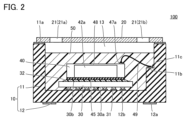
- FIG. 2 is a cross-sectional view of the pressure sensor 100.
- the pressure sensor 100 has a case 10, a lid 20, a semiconductor chip 30, and a MEMS chip 40.
- the pressure sensor 100 may further have a gel material 50.
- the case 10 and the lid 20 form an exterior package body of the pressure sensor 100.
- the lid 20 forms an upper wall of the exterior package body of the pressure sensor 100.
- the case 10 is made of, for example, a ceramic material.
- the case 10 has a side wall 11 and a bottom wall 12.
- the bottom wall 12 is connected to the lower end of the side wall 11.
- the space defined by the side wall 11 and the bottom wall 12 is referred to as an internal space 13.
- the internal space 13 constitutes the internal space of the package exterior of the pressure sensor 100.
- the case 10 is, for example, rectangular in plan view.
- the upper end of the side wall 11 is formed of, for example, a metal layer 11a.
- External connection pads 12a are arranged on the outer wall surface of the bottom wall 12.
- the pressure sensor 100 is electrically connected to a printed wiring board or the like via the external connection pads 12a.
- a plurality of internal connection pads 12b are arranged on the inner wall surface of the bottom wall 12.
- the internal connection pads 12b are electrically connected to the external connection pads 12a via conductors (not shown) embedded in the case 10.
- a step portion 11b is formed on the inner wall surface of the side wall 11.
- An internal connection pad 11c is arranged on the step portion 11b.
- the internal connection pad 11c is electrically connected to the external connection pads 12a and/or the internal connection pads 12b via conductors (not shown) embedded in the case 10.
- the lid 20 is a plate-shaped member.
- the lid 20 is formed, for example, from a metal material.
- the lid 20 is, for example, rectangular in plan view.
- the outer peripheral edge of the lid 20 in plan view is joined to the upper end of the side wall 11. More specifically, the outer peripheral edge of the lid 20 in plan view is welded to the metal layer 11a. In this way, the lid 20 forms the upper wall of the package exterior of the pressure sensor 100.
- the lid 20 has a plurality of holes 21 formed therein.
- the holes 21 penetrate the lid 20 in the thickness direction.
- the internal space 13 communicates with the external space of the package exterior body of the pressure sensor 100 through the holes 21.
- the number of holes 21 is two.
- One of the two holes 21 is hole 21a, and the other of the two holes 21 is hole 21b.
- the holes 21a and 21b are, for example, near the four corners of the lid 20 in a plan view.
- no hole 21 is formed in the center of the lid 20 in a plan view.
- the holes 21a and 21b are, for example, symmetrically positioned with respect to the center of the lid 20 in a plan view.
- the arrangement of the plurality of holes 21 is not limited to this.
- Hole 21 is, for example, circular in plan view.
- the opening diameter of hole 21 is, for example, 20 ⁇ m or more and 300 ⁇ m or less.
- the opening diameter of hole 21 may be 30 ⁇ m or more and 250 ⁇ m or less.
- the shape of hole 21 in plan view does not have to be circular. If the shape of hole 21 in plan view is not circular, the opening diameter of hole 21 is obtained by the square root of the opening area of hole 21 divided by ⁇ /4.
- the semiconductor chip 30 has a first surface 30a and a second surface 30b.
- the first surface 30a and the second surface 30b are end surfaces in the thickness direction of the semiconductor chip 30.
- the semiconductor chip 30 is disposed on the inner wall surface of the bottom wall 12 so that the first surface 30a faces the inner wall surface of the bottom wall 12.
- the semiconductor chip 30 is electrically connected to the internal connection pads 12b by bumps 31.
- the bumps 31 are formed of, for example, gold.
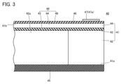
- FIG. 3 is a cross-sectional view of the MEMS chip 40.
- the MEMS chip 40 has a silicon substrate 41, a glass substrate 45, an interlayer insulating film 46, and a plurality of wirings 47.
- the silicon substrate 41 has a first surface 41a and a second surface 41b.
- the first surface 41a and the second surface 41b are end surfaces in the thickness direction of the silicon substrate 41.
- the silicon substrate 41 has a first silicon layer 42, a silicon oxide layer 43, and a second silicon layer 44.
- the silicon oxide layer 43 is disposed on the first silicon layer 42.
- the second silicon layer 44 is disposed on the silicon oxide layer 43. That is, the silicon oxide layer 43 is sandwiched between the first silicon layer 42 and the second silicon layer 44 in the thickness direction of the silicon substrate 41.
- the first silicon layer 42 and the second silicon layer 44 respectively constitute a first surface 41a and a second surface 41b.
- a cavity 42a is formed in the first silicon layer 42.
- the cavity 42a penetrates the first silicon layer 42 in the thickness direction.
- the cavity 42a is closed by the silicon oxide layer 43 and the glass substrate 45.
- the glass substrate 45 is disposed on the first surface 41a.
- resistors 44a and wiring 44b are formed in the second silicon layer 44.
- the second silicon layer 44 in the portion in which the resistors 44a and wiring 44b are formed is doped with impurities.
- the resistors 44a are formed in the second silicon layer 44 above the cavity 42a.
- a portion of the wiring 44b is formed in the second silicon layer 44 above the cavity 42a, and another portion of the wiring 44b is formed in the second silicon layer 44 above the first silicon layer 42 around the cavity 42a.
- the second silicon layer 44 has a plurality of resistors 44a.
- the plurality of resistors 44a are connected to each other by the wiring 44b to form a bridge circuit.
- the interlayer insulating film 46 is formed of, for example, silicon oxide.
- the interlayer insulating film 46 is disposed on the second surface 41b (on the second silicon layer 44).
- the wiring 47 is disposed on the interlayer insulating film 46 above the first silicon layer 42 around the cavity 42a.
- the wiring 47 is formed of, for example, a metal material.
- One end of the wiring 47 is a bonding pad 47a. The other end of the wiring 47 is electrically connected to the wiring 44b.
- the silicon oxide layer 43 on the cavity 42a, the second silicon layer 44 above the cavity 42a, and the interlayer insulating film 46 above the cavity 42a constitute a membrane 48.
- a power supply voltage for example, is applied between a pair of bonding pads 47a electrically connected to the resistor 44a.
- the membrane 48 bends the electrical resistance value of the resistor 44a changes, and the voltage between a pair of bonding pads 47a other than the pair of bonding pads 47a to which the power supply voltage is applied changes from the above power supply voltage.
- the MEMS chip 40 is placed on the semiconductor chip 30 with the adhesive member 32 interposed therebetween so that the glass substrate 45 faces the second surface 30b. As a result, the MEMS chip 40 is placed in the internal space 13. One end of the bonding wire 49 is joined to the bonding pad 47a, and the other end of the bonding wire 49 is joined to the internal connection pad 11c. As a result, the MEMS chip 40 is electrically connected to the semiconductor chip 30 by the bonding wire 49, the conductor embedded inside the case 10, the internal connection pad 12b, and the bump 31.
- the bonding wire 49 is made of, for example, gold.
- the gel material 50 fills the internal space 13. As a result, the semiconductor chip 30 and the MEMS chip 40 are sealed with the gel material 50.
- the pressure change in the external space of the pressure sensor 100 is transmitted to the internal space 13 through the hole 21.
- the membrane 48 is deflected due to the difference with the internal pressure of the cavity 42a.
- the change in the electrical resistance value of the resistor 44a fluctuates the voltage between a pair of bonding pads 47a electrically connected to the resistor 44a.
- This voltage change is output to the semiconductor chip 30, where signal processing is performed, and the pressure in the external space of the package exterior of the pressure sensor 100 is calculated.
- a signal indicating the calculated pressure in the external space of the package exterior of the pressure sensor 100 is output from the semiconductor chip 30 via the external connection pad 12a.
- FIG. 4 is a manufacturing process diagram of the pressure sensor 100. As shown in FIG. 4, the manufacturing method of the pressure sensor 100 includes a preparation process S1, a first chip mounting process S2, a second chip mounting process S3, a wire bonding process S4, a gel filling process S5, and a lid bonding process S6.
- FIG. 5 is a cross-sectional view illustrating the preparation step S1. As shown in FIG. 5, in the preparation step S1, the case 10 is prepared.
- the first chip mounting process S2 is carried out after the preparation process S1.
- FIG. 6 is a cross-sectional view explaining the first chip mounting process S2.
- the semiconductor chip 30 is mounted on the inner wall surface of the bottom wall 12. At this time, the semiconductor chip 30 is electrically connected to the internal connection pads 12b by the bumps 31.
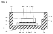
- FIG. 7 is a cross-sectional view illustrating the second chip mounting process S3.
- the MEMS chip 40 is mounted on the semiconductor chip 30.
- uncured adhesive material 32 is applied onto the second surface 30b.
- the MEMS chip 40 is mounted on the second surface 30b with the adhesive material 32 interposed therebetween.
- the adhesive material 32 is heated and cured.
- the wire bonding process S4 is performed after the second chip mounting process S3.
- Figure 8 is a cross-sectional view illustrating the wire bonding process S4. As shown in Figure 8, in the wire bonding process S4, one end of the bonding wire 49 is bonded to the bonding pad 47a, and the other end of the bonding wire 49 is bonded to the internal connection pad 11c.
- FIG. 9 is a cross-sectional view illustrating the gel filling step S5.
- the internal space 13 is filled with a gel material 50.
- the lid bonding step S6 is performed after the gel filling step S5.
- FIG. 10 is a cross-sectional view illustrating the lid bonding step S6.
- an electrode 60 is brought into contact with the outer peripheral edge portion of the lid 20 in a planar view and welded, thereby bonding the outer peripheral edge portion of the lid 20 in a planar view to the upper end of the sidewall 11 (more specifically, the metal layer 11a). In this way, the pressure sensor 100 having the structure shown in FIG. 1 and FIG. 2 is manufactured.
- the pressure sensor 100 may be cleaned. This cleaning is performed while supplying a cleaning liquid from the hole 21 into the internal space 13. During this cleaning, ultrasonic waves may be applied.
- liquid e.g., rainwater or sweat
- the pool of liquid can deflect the membrane 48 or block contact with the outside air, causing malfunction.
- the pressure sensor 100 multiple holes 21 are formed in the lid 20. Therefore, gas or liquid that enters the internal space 13 through one hole 21 (hole 21a in the example of FIG. 1) can easily escape from the internal space 13 through another hole 21 (hole 21b in the example of FIG. 1). Therefore, with the pressure sensor 100, liquid pools or air bubble pools are less likely to remain in the internal space 13, making it possible to suppress insufficient cleaning, damage to the membrane 48, and obstruction of the operation of the membrane 48.
- holes 21a and 21b are located symmetrically with respect to the center of the lid 20 in a plan view, liquid or gas that enters the internal space 13 through one of holes 21a and 21b can easily escape through the other of holes 21a and 21b. Also, in this case, since hole 21 is not formed in the center of the lid 20 in a plan view, the lid 20 can be easily adsorbed and held, improving handling of the lid 20.
- the opening diameter of the hole 21 is small, the flow of liquid through the hole 21 will be slow. Also, if the opening diameter of the hole 21 is small, there is a risk of clogging of the hole 21. On the other hand, if the opening diameter of the hole 21 is large, small particles will easily enter the internal space 13 through the hole 21. Therefore, if the opening diameter of the hole 21 is 20 ⁇ m or more and 300 ⁇ m or less, it is possible to suppress the intrusion of particles into the internal space 13 while ensuring the flow of liquid through the hole 21 and preventing clogging of the hole 21.
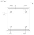
- Fig. 11 is a plan view of the pressure sensor 100 according to the first modification.
- the number of holes 21 formed in the lid 20 may be, for example, four.
- the four holes 21 are holes 21c, 21d, 21e, and 21f.
- Holes 21c, 21d, 21e, and 21f are located near the four corners of the lid 20 in a plan view.
- Holes 21c and 21f are located symmetrically with respect to the center of the lid 20 in a plan view, and holes 21d and 21e are located symmetrically with respect to the center of the lid 20 in a plan view.
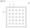
- Fig. 12 is a plan view of a pressure sensor 100 according to a second modified example. As shown in Fig. 12, the holes 21 may be arranged in a lattice pattern in a plan view.
- Pressure sensor 100A The pressure sensor according to the second embodiment is designated as pressure sensor 100A.
- differences from pressure sensor 100 will be mainly described, and overlapping descriptions will not be repeated.
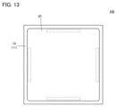
- FIG. 13 is a plan view of pressure sensor 100A.
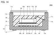
- FIG. 14 is a cross-sectional view of pressure sensor 100A.
- pressure sensor 100A has a case 10, a lid 20, a semiconductor chip 30, and a MEMS chip 40.
- Pressure sensor 100A may further have a gel material 50.
- the configuration of pressure sensor 100A is common to the configuration of pressure sensor 100.
- FIG. 15 is a plan view of the case 10.
- the upper end of the side wall 11 is divided into a plurality of first regions 11d and a plurality of second regions 11e.
- the second regions 11e are located between two adjacent first regions 11d.
- the first regions 11d are preferably located at the four corners of the upper end of the side wall 11 in a plan view.
- FIG. 13 the joints between the outer peripheral edge of the lid 20 in a plan view and the upper end of the side wall 11 are shown by dotted lines.
- the outer peripheral edge of the lid 20 in a plan view is joined only to the second region 11e, and not to the first region 11d.
- the configuration of the pressure sensor 100A differs from the configuration of the pressure sensor 100.
- pressure sensor 100A the outer peripheral edge of lid 20 in a plan view is joined only to second region 11e, so there is a gap between each of the first regions 11d and lid 20. Liquid or gas that enters internal space 13 through one of these gaps is discharged through another of these gaps. Therefore, with pressure sensor 100A, liquid pools or air bubbles are less likely to remain in internal space 13, making it possible to suppress insufficient cleaning, damage to membrane 48, and obstruction of membrane 48 operation.
- the number of joints between the outer peripheral edge of the lid 20 in a plan view and the upper end of the side wall 11 is reduced, so the time required for the lid bonding process S6 is reduced.
- the entire periphery of the side wall 11 is joined to the outer peripheral edge of the lid 20 in a plan view, so there are areas near the upper end of the side wall 11 where liquid is likely to remain.
- a portion of the upper end of the side wall 11 is not joined to the outer peripheral edge of the lid 20 in a plan view, so there are fewer areas where liquid is likely to remain, as described above.
- pressure sensor 100B The pressure sensor according to the third embodiment will be referred to as pressure sensor 100B.
- differences from pressure sensor 100A will be mainly described, and overlapping descriptions will not be repeated.
- FIG. 16 is a plan view of pressure sensor 100B.
- FIG. 17 is a cross-sectional view of pressure sensor 100B.
- pressure sensor 100B has a case 10, a lid 20, a semiconductor chip 30, and a MEMS chip 40.
- Pressure sensor 100B may further have a gel material 50.
- the outer peripheral edge portion of the lid 20 in a plan view is bonded only to the second region 11e.
- no hole 21 is formed in the lid 20.
- the configuration of pressure sensor 100A is common to the configuration of pressure sensor 100.
- pressure sensor 100B there are multiple notches 22 on the outer peripheral edge of lid 20 in plan view.
- the internal space 13 is exposed from the notches 22.
- the internal space 13 exposed from the notches 22 is, for example, triangular (right-angled triangular) in plan view.
- the two notches 22 are notches 22a and 22b, respectively. It is preferable that notches 22a and 22b are located symmetrically with respect to the center of lid 20 in plan view. In these respects, the configuration of pressure sensor 100B differs from the configuration of pressure sensor 100A.
- Fig. 18 is a plan view of a pressure sensor 100B according to a first modified example.
- the number of notches 22 in the outer peripheral edge portion of the lid 20 in a plan view may be four. In other words, the number of notches 22 is not particularly limited.
- Fig. 19A is a plan view of a pressure sensor 100B according to a second modified example.
- Fig. 19B is a plan view of a pressure sensor 100B according to a third modified example.
- the internal space 13 exposed from the notch 22 does not have to be triangular in plan view.
- the notch 22 is located at the four corners of the lid 20 in plan view, and the internal space 13 exposed from the notch 22 may be substantially rectangular in plan view.
- the lid 20 may be cross-shaped in plan view.
- the notches 22 may be formed on opposing sides of the outer peripheral edge of the lid 20 in a plan view.
- the internal space 13 exposed through the notches 22 has a rectangular shape in a plan view.
- Sample 1 has a similar configuration to pressure sensor 100, except that there is only one hole 21 (only hole 21a) formed in the lid 20.
- Sample 2 has a similar configuration to pressure sensor 100B, except that there is only one notch 22 (only notch 22a) on the outer peripheral edge of the lid 20 in a plan view.
- Sample 3 has a similar configuration to pressure sensor 100B, and sample 4 has a similar configuration to pressure sensor 100B according to the first modified example.
- Samples 1 to 4 were immersed in water and then taken out into the air. After that, it was checked with a microscope whether or not a pool of liquid remained in the internal space 13. In Samples 1 and 2, it was confirmed that a pool of liquid remained in the internal space 13 after being taken out into the air. From this, it can be understood that when the lid 20 has only one hole 21 or notch 22, there is a risk that a pool of liquid may remain in the internal space 13.
- ⁇ Appendix 1> a package outer body having a top wall; and a MEMS chip.
- the MEMS chip has a membrane and is disposed in an internal space of the package exterior body;
- the package exterior further includes a case and a lid,
- the case has a side wall and a bottom wall connected to a lower end of the side wall, an outer peripheral edge portion of the lid in a plan view is joined to an upper end of the side wall; 2.
- ⁇ Appendix 3> Further comprising a gel material; 3. The pressure sensor according to claim 2, wherein the gel material is filled in the internal space so as to seal the MEMS chip.
- Appendix 4 A pressure sensor as described in Appendix 2 or Appendix 3, wherein a first hole, which is one of the plurality of holes, is located symmetrically with a second hole, which is another of the plurality of holes, with respect to the center of the lid in a planar view.
- the case has a side wall and a bottom wall connected to a lower end of the side wall, The upper end of the side wall is divided into a plurality of first regions and a plurality of second regions in a plan view, each of the first regions is between two adjacent ones of the second regions; an outer peripheral edge portion of the lid in a plan view is joined only to the second regions;
- the MEMS chip has a membrane and is disposed in the internal space of the package exterior body, forming a pressure sensor.
- ⁇ Appendix 8> Further comprising a gel material; 8. The pressure sensor of claim 7, wherein the gel material is filled in the internal space so as to seal the MEMS chip.
- the outer periphery has a plurality of notches, 9.
- Appendix 10 A pressure sensor as described in Appendix 9, wherein a first notch, one of the plurality of notches, is located symmetrically with respect to a center of the lid in a planar view relative to a second notch, another of the plurality of notches.
- 100, 100A, 100B pressure sensor 10 case, 11 side wall, 11a metal layer, 11b step portion, 11c internal connection pad, 11d first region, 11e second region, 12 bottom wall, 12a external connection pad, 12b internal connection pad, 13 internal space, 20 lid, 21 hole, 21a, 21b, 21c, 21d, 21e, 21f hole, 22 notch, 22a, 22b notch, 30 semiconductor chip, 30a first surface, 30b second surface, 31 bump, 32 adhesive member, 40 MEMS chip, 4 1 silicon substrate, 41a first surface, 41b second surface, 42 first silicon layer, 42a cavity, 43 silicon oxide layer, 44 second silicon layer, 44a resistor, 44b wiring, 45 glass substrate, 46 interlayer insulating film, 47 wiring, 47a bonding pad, 48 membrane, 49 bonding wire, 50 gel material, 60 electrode, S1 preparation step, S2 first chip mounting step, S3 second chip mounting step, S4 wire bonding step, S5 gel filling step, S6 lid bonding step.
Landscapes
- Physics & Mathematics (AREA)
- General Physics & Mathematics (AREA)
- Pressure Sensors (AREA)
Priority Applications (1)
| Application Number | Priority Date | Filing Date | Title |
|---|---|---|---|
| JP2024555674A JPWO2024075462A1 (https=) | 2022-10-03 | 2023-09-06 |
Applications Claiming Priority (2)
| Application Number | Priority Date | Filing Date | Title |
|---|---|---|---|
| JP2022159577 | 2022-10-03 | ||
| JP2022-159577 | 2022-10-03 |
Publications (1)
| Publication Number | Publication Date |
|---|---|
| WO2024075462A1 true WO2024075462A1 (ja) | 2024-04-11 |
Family
ID=90607800
Family Applications (1)
| Application Number | Title | Priority Date | Filing Date |
|---|---|---|---|
| PCT/JP2023/032460 Ceased WO2024075462A1 (ja) | 2022-10-03 | 2023-09-06 | 圧力センサ |
Country Status (2)
| Country | Link |
|---|---|
| JP (1) | JPWO2024075462A1 (https=) |
| WO (1) | WO2024075462A1 (https=) |
Cited By (1)
| Publication number | Priority date | Publication date | Assignee | Title |
|---|---|---|---|---|
| CN119595174A (zh) * | 2024-12-13 | 2025-03-11 | 深圳瑞德感知科技有限公司 | 新型无隔离膜片的mems压力传感器 |
Citations (4)
| Publication number | Priority date | Publication date | Assignee | Title |
|---|---|---|---|---|
| JP2001272294A (ja) * | 2000-01-25 | 2001-10-05 | Motorola Inc | 選択封止付き超小型電気機械式システム・センサおよびそのための方法 |
| WO2010059433A2 (en) * | 2008-11-07 | 2010-05-27 | The Charles Stark Draper Laboratory, Inc. | Mems dosimeter |
| WO2013065540A1 (ja) * | 2011-11-04 | 2013-05-10 | アルプス電気株式会社 | 圧力センサ装置 |
| US9011776B2 (en) * | 2012-08-30 | 2015-04-21 | STMicoroelectronics S.r.l. | Packaged device exposed to environmental air and liquids and manufacturing method thereof |
-
2023
- 2023-09-06 WO PCT/JP2023/032460 patent/WO2024075462A1/ja not_active Ceased
- 2023-09-06 JP JP2024555674A patent/JPWO2024075462A1/ja active Pending
Patent Citations (4)
| Publication number | Priority date | Publication date | Assignee | Title |
|---|---|---|---|---|
| JP2001272294A (ja) * | 2000-01-25 | 2001-10-05 | Motorola Inc | 選択封止付き超小型電気機械式システム・センサおよびそのための方法 |
| WO2010059433A2 (en) * | 2008-11-07 | 2010-05-27 | The Charles Stark Draper Laboratory, Inc. | Mems dosimeter |
| WO2013065540A1 (ja) * | 2011-11-04 | 2013-05-10 | アルプス電気株式会社 | 圧力センサ装置 |
| US9011776B2 (en) * | 2012-08-30 | 2015-04-21 | STMicoroelectronics S.r.l. | Packaged device exposed to environmental air and liquids and manufacturing method thereof |
Cited By (1)
| Publication number | Priority date | Publication date | Assignee | Title |
|---|---|---|---|---|
| CN119595174A (zh) * | 2024-12-13 | 2025-03-11 | 深圳瑞德感知科技有限公司 | 新型无隔离膜片的mems压力传感器 |
Also Published As
| Publication number | Publication date |
|---|---|
| JPWO2024075462A1 (https=) | 2024-04-11 |
Similar Documents
| Publication | Publication Date | Title |
|---|---|---|
| JP4481323B2 (ja) | 物理量センサ及びその製造方法 | |
| JP5486271B2 (ja) | 加速度センサ、及び加速度センサの製造方法 | |
| JP5218455B2 (ja) | 半導体力学量センサおよびその製造方法 | |
| JP2009004507A (ja) | 電子部品用パッケージ及びその製造方法と電子部品装置 | |
| TWI464835B (zh) | 半導體封裝體及其製造方法 | |
| EP1860418A1 (en) | A method for fabricating a pressure sensor using SOI wafers | |
| CN101427365A (zh) | 半导体传感器件及其制造方法 | |
| JP7408764B2 (ja) | Mems素子およびmemsモジュール | |
| TWI455265B (zh) | 具微機電元件之封裝結構及其製法 | |
| WO2024075462A1 (ja) | 圧力センサ | |
| JP7455585B2 (ja) | センサユニットならびに基板およびキャリアを相互接続する方法 | |
| JP4675945B2 (ja) | 半導体装置 | |
| KR100620810B1 (ko) | Mems 소자 패키지 및 그 제조방법 | |
| KR20100112699A (ko) | 가스 센싱 장치 및 가스 센싱 장치의 제조 방법 | |
| US12464951B2 (en) | Vibration device | |
| JP4219876B2 (ja) | 容量式湿度センサ及びその製造方法 | |
| JP2006128683A (ja) | パッケージング基板の製造方法およびそれを用いたパッケージング方法 | |
| JP2013098514A (ja) | 半導体装置の製造方法及び半導体装置、電子機器 | |
| JP2011104767A (ja) | ウェーハ・レベル・パッケージに関するシリコン・タブ・エッジ・マウント | |
| JP4273356B2 (ja) | 半導体装置の製造方法 | |
| JP2012216868A (ja) | 電子部品用パッケージ及び電子部品装置 | |
| JPWO2012102252A1 (ja) | 貫通電極付基板およびその製造方法 | |
| JP2010181243A (ja) | 容量式力学量センサ装置の製造方法 | |
| JP2007042786A (ja) | マイクロデバイス及びそのパッケージング方法 | |
| CN102315189B (zh) | 半导体衬底上的键合接触部位 |
Legal Events
| Date | Code | Title | Description |
|---|---|---|---|
| 121 | Ep: the epo has been informed by wipo that ep was designated in this application |
Ref document number: 23874591 Country of ref document: EP Kind code of ref document: A1 |
|
| WWE | Wipo information: entry into national phase |
Ref document number: 2024555674 Country of ref document: JP |
|
| NENP | Non-entry into the national phase |
Ref country code: DE |
|
| 122 | Ep: pct application non-entry in european phase |
Ref document number: 23874591 Country of ref document: EP Kind code of ref document: A1 |