WO2024070518A1 - 配線基板 - Google Patents
配線基板 Download PDFInfo
- Publication number
- WO2024070518A1 WO2024070518A1 PCT/JP2023/032240 JP2023032240W WO2024070518A1 WO 2024070518 A1 WO2024070518 A1 WO 2024070518A1 JP 2023032240 W JP2023032240 W JP 2023032240W WO 2024070518 A1 WO2024070518 A1 WO 2024070518A1
- Authority
- WO
- WIPO (PCT)
- Prior art keywords
- wiring
- substrate
- main surface
- wiring board
- wirings
- Prior art date
- Legal status (The legal status is an assumption and is not a legal conclusion. Google has not performed a legal analysis and makes no representation as to the accuracy of the status listed.)
- Ceased
Links
Images










Classifications
-
- H—ELECTRICITY
- H05—ELECTRIC TECHNIQUES NOT OTHERWISE PROVIDED FOR
- H05K—PRINTED CIRCUITS; CASINGS OR CONSTRUCTIONAL DETAILS OF ELECTRIC APPARATUS; MANUFACTURE OF ASSEMBLAGES OF ELECTRICAL COMPONENTS
- H05K1/00—Printed circuits
- H05K1/02—Details
- H05K1/14—Structural association of two or more printed circuits
- H05K1/142—Arrangements of planar printed circuit boards in the same plane, e.g. auxiliary printed circuit insert mounted in a main printed circuit
-
- H—ELECTRICITY
- H05—ELECTRIC TECHNIQUES NOT OTHERWISE PROVIDED FOR
- H05K—PRINTED CIRCUITS; CASINGS OR CONSTRUCTIONAL DETAILS OF ELECTRIC APPARATUS; MANUFACTURE OF ASSEMBLAGES OF ELECTRICAL COMPONENTS
- H05K1/00—Printed circuits
- H05K1/02—Details
-
- H—ELECTRICITY
- H05—ELECTRIC TECHNIQUES NOT OTHERWISE PROVIDED FOR
- H05K—PRINTED CIRCUITS; CASINGS OR CONSTRUCTIONAL DETAILS OF ELECTRIC APPARATUS; MANUFACTURE OF ASSEMBLAGES OF ELECTRICAL COMPONENTS
- H05K1/00—Printed circuits
- H05K1/02—Details
- H05K1/0277—Bendability or stretchability details
- H05K1/0283—Stretchable printed circuits
-
- H—ELECTRICITY
- H05—ELECTRIC TECHNIQUES NOT OTHERWISE PROVIDED FOR
- H05K—PRINTED CIRCUITS; CASINGS OR CONSTRUCTIONAL DETAILS OF ELECTRIC APPARATUS; MANUFACTURE OF ASSEMBLAGES OF ELECTRICAL COMPONENTS
- H05K1/00—Printed circuits
- H05K1/02—Details
- H05K1/14—Structural association of two or more printed circuits
-
- H—ELECTRICITY
- H05—ELECTRIC TECHNIQUES NOT OTHERWISE PROVIDED FOR
- H05K—PRINTED CIRCUITS; CASINGS OR CONSTRUCTIONAL DETAILS OF ELECTRIC APPARATUS; MANUFACTURE OF ASSEMBLAGES OF ELECTRICAL COMPONENTS
- H05K2201/00—Indexing scheme relating to printed circuits covered by H05K1/00
- H05K2201/01—Dielectrics
- H05K2201/0104—Properties and characteristics in general
- H05K2201/0129—Thermoplastic polymer, e.g. auto-adhesive layer; Shaping of thermoplastic polymer
-
- H—ELECTRICITY
- H05—ELECTRIC TECHNIQUES NOT OTHERWISE PROVIDED FOR
- H05K—PRINTED CIRCUITS; CASINGS OR CONSTRUCTIONAL DETAILS OF ELECTRIC APPARATUS; MANUFACTURE OF ASSEMBLAGES OF ELECTRICAL COMPONENTS
- H05K2201/00—Indexing scheme relating to printed circuits covered by H05K1/00
- H05K2201/09—Shape and layout
- H05K2201/09209—Shape and layout details of conductors
- H05K2201/09218—Conductive traces
- H05K2201/09236—Parallel layout
Definitions
- This disclosure relates to a wiring board.
- a conventional wiring board is described in JP-A-7-94861 (Patent Document 1).
- This wiring board is made by forming a heat-adhesive insulating resist on a first substrate and a second substrate, forming an electrode pattern on the insulating resist, and pressing the electrode patterns of the substrates against each other, and then heat-adhering the resist around the electrode pattern in the pressed state.
- the wiring board has two layers of insulating resist between the first substrate and the second substrate. The first substrate and the second substrate are connected via the two layers of insulating resist.
- the purpose of this disclosure is to provide a wiring board that can be made thinner.
- a wiring board comprises: A first substrate having a first major surface; a second substrate having a second major surface; A first wiring disposed on the first main surface; a second wiring disposed on the second main surface, the first main surface and the second main surface are in contact with each other, and the first base material and the second base material are connected to each other; The first wiring and the second wiring are electrically connected to each other and opposed to each other in a thickness direction of the first base material.
- the wiring board according to one aspect of the present invention can be made thinner.
- FIG. 1 is an exploded perspective view of a wiring board according to a first embodiment of the present invention.
- FIG. 2 is an exploded plan view of the wiring board.
- FIG. 3 is a plan view of the wiring board.
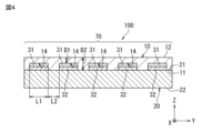
- FIG. 4 is a cross-sectional view taken along line IV-IV of FIG.
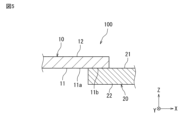
- FIG. 5 is a cross-sectional view taken along line VV of FIG.
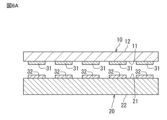
- FIG. 6A is a cross-sectional view illustrating a method for manufacturing a wiring board.
- FIG. 6B is a cross-sectional view illustrating the method for manufacturing the wiring board.
- FIG. 7 is a cross-sectional view of a wiring board according to a second embodiment of the present invention.
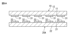
- FIG. 8A is a cross-sectional view illustrating a method for manufacturing a wiring board.
- FIG. 8B is a cross-sectional view illustrating the method for manufacturing the wiring board.
- FIG. 9 is a plan view of a wiring board according to a third embodiment of the present invention.
- FIG. 10 is a cross-sectional view taken along line XX of FIG.
- FIG. 11 is a cross-sectional view of a wiring board according to a fourth embodiment of the present invention.
- FIG. 12 is a cross-sectional view of a wiring board according to a fifth embodiment of the present invention.
- FIG. 13 is a cross-sectional view of a first modified example of the wiring board according to the fifth embodiment.
- FIG. 14 is a cross-sectional view of a second modified example of the wiring board according to the fifth embodiment.
- FIG. 15 is a cross-sectional view of a wiring board according to the sixth embodiment.
- FIG. 16 is a plan view of the wiring board according to the seventh embodiment.
- FIG. 17 is a cross-sectional view taken along line XVII-XVII of FIG.
- FIG. 18 is a cross-sectional view of a wiring board according to the eighth embodiment.
- FIG. 19 is a cross-sectional view of a wiring board according to the ninth embodiment.
- FIG. 20 is a cross-sectional view of a wiring board according to the tenth embodiment.
- Figure 1 is an exploded perspective view of the wiring board according to the first embodiment of the present invention.
- Figure 2 is an exploded plan view of the wiring board.
- Figure 3 is a plan view of the wiring board.
- Figure 4 is a cross-sectional view taken along line IV-IV in Figure 3.
- Figure 5 is a cross-sectional view taken along line V-V in Figure 3.
- the arrow Z indicates a direction parallel to the thickness direction of the first substrate and extending from the first main surface to the third main surface of the first substrate.
- the thickness direction may be either the forward Z direction or the reverse Z direction.
- the thickness direction of the second substrate is also parallel to the Z direction.
- the arrow X indicates a direction parallel to the extension direction of the first substrate and extending from a position of the first substrate that is far from the second substrate to a position of the first substrate that is close to the second substrate.
- the extension direction of the first substrate may be either the forward X direction or the reverse X direction.
- the extension directions of the first wiring, the second substrate, and the second wiring are also parallel to the X direction.
- the X direction and the Z direction are perpendicular to each other, and the direction perpendicular to the X direction and the Z direction is the Y direction.
- the wiring board 100 comprises a first substrate 10 having a first main surface 11, a second substrate 20 having a second main surface 21, a first wiring 31 arranged on the first main surface 11, and a second wiring 32 arranged on the second main surface 21.
- the wiring board 100 is used for circuit connection with, for example, a printed circuit board or a flexible board.
- the first substrate 10 is a support material such as a film material made of a stretchable resin material.
- the first substrate 10 is in the form of a sheet or film.
- the first substrate 10 has a first main surface 11 and a third main surface 12 located on opposite sides.
- the first substrate 10 has a recess 14 on the first main surface 11 (see FIG. 4).
- the recess 14 exists at least in the region 70 where the first substrate 10 and the second substrate 20 overlap when viewed from the Z direction.
- the recess 14 corresponds to a portion of the first substrate 10 recessed in the Z direction (i.e., the thickness direction of the first substrate 10) on the first main surface 11. Therefore, the inner surface of the recess 14 can also be interpreted as a surface that forms a recess in the first main surface 11.
- the first main surface 11 may be composed of the inner surface of the recess 14 and a flat surface other than the recess 14.
- the recess 14 may extend along the X direction.
- the third main surface 12 is an exposed surface in this embodiment.
- the material of the first substrate 10 may be, for example, a thermoplastic resin.
- the material of the first substrate 10 is a resin material having elasticity, and may include, for example, a styrene resin, an olefin resin, an epoxy resin, a urethane resin, an acrylic resin, and/or a silicone resin. More specifically, the material may be thermoplastic polyurethane (TPU), polyethylene (PE), and the like.
- TPU thermoplastic polyurethane
- PE polyethylene
- the resin material has a softening point. Specifically, it is more preferable that the softening point is 90 degrees or higher. This makes it easier for the first main surface 11 of the first substrate 10 and the second main surface 21 of the second substrate 20 to come into contact with each other.
- the first substrate 10 is stretchable.
- the first substrate 10 is stretchable, which reduces the risk of breakage due to expansion and contraction during use of the wiring board 100.
- the thickness of the first substrate 10 is not particularly limited, but from the viewpoint of not inhibiting the expansion and contraction of the surface of the living body when attached to the living body, it is preferably 160 ⁇ m or less, and more preferably 80 ⁇ m or less. In addition, the thickness of the first substrate 10 is preferably 40 ⁇ m or more.
- the second substrate 20 has a second main surface 21 and a fourth main surface 22 located on opposite sides to each other.
- the end of the second substrate 20 in the X direction overlaps with the end of the first substrate 10 in the X direction. More specifically, the end of the second substrate 20 in the reverse X direction overlaps with the end of the first substrate 10 in the forward X direction.
- the second main surface 21 faces the first main surface 11.
- the fourth main surface 22 is an exposed surface. Note that the fourth main surface 22 does not have to be exposed.
- the second substrate 20 is a substrate different from the first substrate 10, and may be, for example, a rigid substrate or a flexible substrate.
- a rigid substrate for example, a glass epoxy substrate is used, which is manufactured by impregnating layers of glass fiber cloth with epoxy resin.
- a flexible substrate for example, polyimide, a plastic with excellent heat resistance, is used.
- the first substrate 10 and the second substrate 20 are connected by contacting the second main surface 21 of the second substrate 20 with the first main surface 11 of the first substrate 10 (see FIG. 3).
- the first substrate 10 and the second substrate 20 are connected by direct contact without the need for insulating resist, so compared to contact via conventional insulating resist, the thickness of the entire device can be made thinner by the thickness of the insulating resist.
- the insulating resist is no longer required, printing of the insulating resist is also no longer necessary. This allows the manufacturing costs and labor of the wiring substrate to be reduced.
- the first main surface 11 of the first substrate 10 and the second main surface 21 of the second substrate 20 are in contact with each other and bonded together.
- Bonding can be, for example, thermocompression bonding, welding, fusion bonding, etc.
- adhesion means the ability to withstand a tensile force of 20 N.
- Evaluation of the adhesive strength between the first substrate 10 and the second substrate 20 can be performed based on JIS K 6849.
- Adhesion through contact means that the first main surface 11 of the first substrate 10 and the second main surface 21 of the second substrate 20 are directly attached to each other without the use of any other member such as an adhesive.
- the first substrate 10 and the second substrate 20 come into contact through surface contact between the first main surface 11 and the second main surface 21, improving the connection strength between the first substrate 10 and the second substrate 20.
- the method for bringing the first and second main surfaces into contact is not particularly limited, but for example, the first substrate 10 and the second substrate 20 may be connected to the side surfaces of the first substrate 10 and the second substrate 20 via a separate member, so that the first and second main surfaces come into contact.
- the interface is the portion where an extended surface extended from a non-overlapping surface of the first main surface 11 that does not overlap with the second main surface 21 to be flush with the non-overlapping surface overlaps with the region where the first main surface 11 and the second main surface 21 contact each other.
- the extended surface 11b of the flat surface 11a (non-overlapping surface) of the first main surface 11 located in the region where the first main surface 11 and the second main surface 21 do not contact each other is the interface between the first main surface 11 and the second main surface 21.
- the extended surface 11b is a surface that is substantially flush with the flat surface 11a in the contact region between the first substrate 10 and the second substrate 20. It goes without saying that the extended surface is a virtual surface. The same applies to the following embodiments.
- the first wiring 31 is disposed on the first main surface 11 of the first substrate 10. At least in the region 70 where the first substrate 10 and the second substrate 20 overlap, the first wiring 31 has a shape that extends in one direction. Specifically, the first wiring 31 may extend along the X direction. There may be multiple first wirings 31. Multiple first wirings 31 may be disposed parallel to each other along the Y direction. The shape of the first wiring 31 is not particularly limited.
- the first wiring 31 is formed of a conductive material.
- the conductive material may be a metal foil such as silver, copper, or nickel, or a mixture of a metal powder such as silver, copper, or nickel and an elastomeric resin such as an epoxy resin or a silicone resin.
- the first wiring 31 is preferably elastic.
- the first wiring 31 is disposed in the first recess 14 of the first substrate 10.
- the first wiring 31 may be disposed on the first main surface 11 so as to be fitted into the first recess 14. This can also be interpreted as the first wiring 31 being disposed in the first recess 14 and extending along the first recess 14.
- one first wiring 31 is disposed in one first recess 14. That is, each of the multiple first wirings 31 may be disposed separately in each of the multiple first recesses 14.
- the first substrate 10 is present between two first wirings 31 adjacent to each other in the Y direction. This ensures insulation between the two first wirings 31 adjacent to each other. From the viewpoint of making the entire wiring board thinner, it is preferable that the thickness of the first wiring 31 is 30 ⁇ m or less.
- the second wiring 32 is disposed in the first recess 14 of the first substrate 10. At least in the region 70 where the first substrate 10 and the second substrate 20 overlap, the second wiring 32 has a shape that extends in one direction. Specifically, the second wiring 32 may extend along the X direction. There may be multiple second wirings 32. The multiple second wirings 32 may be disposed parallel to each other in the Y direction. The shape of the second wiring 32 is not particularly limited.
- the second wiring 32 is formed of a conductive material.
- the conductive material may be a metal foil such as silver, copper, or nickel, or a mixture of a metal powder such as silver, copper, or nickel and an elastomeric resin such as an epoxy resin or a silicone resin.
- the second wiring 32 is elastic.
- the first wiring 31 and the second wiring 32 are electrically connected facing each other in the Z direction (thickness direction of the first substrate). Specifically, the first wiring 31 and the second wiring 32 are in direct contact and electrically connected. Note that the first wiring 31 and the second wiring 32 may be electrically connected via a conductive member disposed between the first wiring 31 and the second wiring 32.
- the second wiring 32 may be in contact with the first wiring 31 arranged in the first recess 14.
- the first wiring 31 and the second wiring 32 may be in contact with each other at the first recess 14 in a cross-sectional view.
- the first main surface 11 and the second main surface 21 may be in contact with each other on the flat surface of the first main surface 11 (see FIG. 4).
- the interface between the first wiring 31 and the second wiring 32 and the interface between the first main surface 11 and the second main surface 21 are located on different planes.
- the strength against peeling at the adhesive surface between the first substrate 10 and the second substrate 20 can be improved.
- the multiple second wirings 32 are arranged side by side in the Y direction.
- the ratio L1/L2 of the width L1 of the second wiring 32 to the width L2 between two adjacent second wirings 32 in the Y direction is 1 or more and 20 or less.
- the ratio of L1/L2 is 20 or less, the insulation between the two adjacent second wirings 32 can be suitably ensured.
- the connection strength between the first substrate 10 and the second substrate 20 is improved.
- the ratio of L1/L2 is 1 or more, a larger second wiring 32 can be ensured, and the electrical resistance of the second wiring 32 can be reduced.
- the multiple second wirings 32 at least two second wirings 32 adjacent to each other in the Y direction only need to satisfy the above configuration, and preferably, all second wirings 32 only need to satisfy the above configuration. Similarly, it is more preferable that the width of the first wiring 31 and the distance between two adjacent first wirings 31 also satisfy the above relationship.
- the width L1 of the second wiring 32 is the size in the direction perpendicular to the extension direction of the second wiring 32 when viewed from the Z direction.
- the width L1 of the second wiring 32 is the size of the second wiring 32 in the Y direction.
- the width L1 of the second wiring 32 is the maximum width of the second wiring 32. If it is difficult to measure the maximum width of the second wiring 32, the average width of the second wiring 32 is taken as L1.
- the width of the first wiring 31 may be the same as the width L1 of the second wiring 32.
- the width L2 between two adjacent second wirings 32 in the Y direction is the shortest distance in the Y direction between two adjacent second wirings 32. If it is difficult to measure the shortest distance in the Y direction between the second wirings 32, the average value of the width between two adjacent second wirings 32 in the Y direction is taken as L2.
- the average value refers to the average value of the measurement values obtained by measuring the width of one second wiring 32 at three different points along the extension direction (X direction) in the area where the first substrate 10 and the second substrate 20 overlap.
- the second wirings 32 are arranged side by side in the Y direction.
- the ratio S1/S2 of the area S1 of a region 71 (hereinafter referred to as the first region 71) where the second wirings 32 exist and the area S2 of a region 72 (hereinafter referred to as the second region 72) between two second wirings 32 adjacent in the Y direction is preferably 1 or more and 20 or less.
- the first region 71 is a region of one second wiring 32 in the overlapping region 70 of the first substrate 10 and the second substrate 20 when viewed from the Z direction.
- the second region 72 is a region between two first regions 71 adjacent to each other in the Y direction when viewed from the Z direction.
- the first region 71 and the second region 72 are shown hatched in FIG. 3.
- the first region 71 and the second region 72 may each have a rectangular shape. In the X direction, the first region 71 and the second region 72 have the same length. Note that the shapes of the first region 71 and the second region 72 are not limited to rectangular.
- ratio S1/S2 20 By making the ratio S1/S2 20 or less, it is possible to ensure suitable insulation between two adjacent second wirings 32. Also, it is possible to ensure the contact area between the first main surface 11 and the second main surface 21. This improves the connection strength between the first substrate 10 and the second substrate 20. Also, by making the ratio S1/S2 1 or more, it is possible to arrange larger second wirings 32, thereby reducing the electrical resistance of the second wirings 32.
- the distance D1 from the first wiring 31 to the third main surface 12 of the first substrate 10 is smaller than the distance D2 from the interface between the first substrate 10 and the second substrate 20 to the third main surface 12 of the first substrate 10 (see FIG. 4).
- the distance D1 refers to the minimum value between the first wiring 31 and the third main surface 12
- the distance D2 refers to the minimum value between the interface between the first substrate 10 and the second substrate 20 and the third main surface 12. This allows the shape of the third main surface 12 of the first substrate 10 to be made flatter.
- the distance D2 is equal to or greater than the sum of the thickness of the first wiring 31 and the thickness of the second wiring 32.
- the thickness of the first substrate 10 in the portion overlapping with the first wiring 31 as viewed from the Z direction can be reduced. It is predicted that the substrate in the portion overlapping with the wiring as viewed from the Z direction will have a reduced elasticity. According to the above structure, the thickness of the substrate can be reduced in the area where a decrease in elasticity is expected, so if the first substrate 10 has elasticity, the elasticity of the first substrate 10 is good.
- first wirings 31 are formed on the first main surface 11 of the first substrate 10.
- second wirings 32 are formed on the second main surface 21 of the second substrate 20.
- the first substrate 10 and the second substrate 20 are overlapped so that the first wirings 31 and the second wirings 32 face each other in the Z direction (i.e., the thickness direction of the substrates).
- the overlapped first substrate 10 and the second substrate 20 are then thermocompression bonded together. This may be performed, for example, by pressing a heater against the third main surface 12 of the first substrate 10.
- the first substrate 10 flows into spaces where no wiring is arranged, such as spaces between multiple wirings adjacent to each other in the Y direction, due to pressure and heat from the heater.
- the flowing first substrate 10 comes into contact with the second substrate 20 while covering the first wiring 31 and the second wiring 32.
- the first main surface 11 of the first substrate 10 and the second main surface 21 of the second substrate 20 are thermocompression-bonded, and the first wiring 31 and the second wiring 32 are arranged in the first recess 14. Since the first substrate 10 has a softening point, it becomes easy to flow when the first substrate 10 is heated, and it becomes easy to come into contact with the second substrate 20.
- the first substrate 10 having a softening point is suitable for thermocompression bonding.
- the first substrate 10 has thermoplasticity, it is also suitable for thermocompression bonding.
- the thermocompression bonding method is not particularly limited, and for example, another heater may be pressed against the fourth main surface 22 of the second substrate 20.
- Fig. 7 is a cross-sectional view of a wiring board 100A according to the second embodiment.
- Fig. 7 corresponds to Fig. 4 of the first embodiment.
- the wiring board 100A according to the second embodiment is different from the wiring board 100 according to the first embodiment in the structure of the second base material 20A.
- the second substrate 20A has a second main surface 21 and a fourth main surface 22 located on opposite sides.
- the first substrate 10 has a first recess 14 on the first main surface 11, and the second substrate 20A has a second recess 24 on the second main surface 21.
- the first wiring 31 is disposed in the first recess 24, and the second wiring 32 is disposed in the second recess 24.
- One first wiring 31 is disposed in one first recess 14.
- One second wiring 32 is disposed in one second recess 24.
- the first wiring 31 is disposed in the first recess 14, so that the first substrate 10 exists between two first wirings 31 that are adjacent to each other in the Y direction. This ensures insulation between two adjacent first wirings 31.
- the second wiring 32 is disposed in the second recess 24, so that the second substrate 20A exists between two second wirings 32 that are adjacent to each other in the Y direction. This ensures insulation between two adjacent second wirings 32.
- recesses 14, 24 are provided in the first substrate 10 and the second substrate 20A, respectively, and wiring 31, 32 are arranged in each recess 14, 24. This allows the thickness of the first substrate 10 and the second substrate 20A to be further reduced, thereby making it possible to further thin the wiring board.
- the second substrate 20A is a substrate having the same elasticity as the first substrate 10, and is, for example, a thermoplastic resin.
- the thermoplastic resin include thermoplastic polyurethane (TPU) and polyethylene (PE).
- the thermoplastic resin has a softening point, and the softening point is, for example, 90 degrees or more.
- the shape of the second substrate 20A is preferably a sheet or film.
- the thickness of the second substrate 20A is not particularly limited, but is preferably 160 ⁇ m or less, and more preferably 80 ⁇ m or less, from the viewpoint of not inhibiting the expansion and contraction of the surface of the living body when attached to the living body. In addition, the thickness of the second substrate 20A is preferably 40 ⁇ m or more.
- the material of the second substrate 20A is preferably the same as that of the first substrate. By using the same material as that of the first substrate 10, the amount of expansion and contraction of the entire wiring board can be made closer to uniform.
- the first substrate 10 and the second substrate 20A may be made of different materials.
- the distance between the second wiring 32 and the fourth main surface 22 of the second substrate 20A can also be reduced for the second substrate 20A.
- the thickness of the second substrate 20A at the portion overlapping with the second wiring 32 when viewed from the Z direction can be reduced, so that if the second substrate 20A has elasticity, the elasticity of the second substrate 20A is good.
- the first main surface 11 and the second main surface 21 are in contact and bonded.
- the first wiring 31 and the second wiring 32 are in contact facing each other in the Z direction.
- the interface between the first wiring 31 and the second wiring 32 and the interface between the first main surface 11 and the second main surface 21 are located on the same plane. That is, the contact surface between the wirings and the contact surface between the substrates are located on the same plane. By matching the interfaces, the amount of expansion and contraction on the first substrate 10 side and the second substrate 20A side can be made closer to uniform. Note that the interface between the first wiring 31 and the second wiring 32 and the interface between the first main surface 11 and the second main surface 21 do not have to be located on the same plane.
- a plurality of first wirings 31 are formed on the first main surface 11 of the first substrate 10.
- a plurality of second wirings 32 are formed on the second main surface 21 of the second substrate 20A.
- the first substrate 10 and the second substrate 20A are overlapped so that the first wirings 31 and the second wirings 32 face each other in the Z direction.
- heaters are pressed against the third main surface 12 of the first substrate 10 and the fourth main surface 22 of the second substrate 20A, respectively, and the first substrate 10 and the second substrate 20A are heated by the heaters.
- the first substrate 10 flows between two adjacent first wirings 31 due to pressure and heat from the heater.
- the second substrate 20A also flows between two adjacent second wirings 32.
- the flowing first substrate 10 and second substrate 20A come into contact with each other while covering the first wiring 31 and the second wiring 32.
- This causes the first main surface 11 of the first substrate 10 and the second main surface 21 of the second substrate 20A to be thermocompression bonded.
- the first wiring 31 is disposed in the first recess 14, and the second wiring 32 is disposed in the second recess 24.
- the first substrate 10 and the second substrate 20A have softening points, so that the first substrate 10 and the second substrate 20A tend to flow when heated and tend to come into contact with each other. In other words, they are suitable for thermocompression bonding.
- the first substrate 10 and the second substrate 20A also have thermoplasticity, so they are similarly suitable for thermocompression bonding.
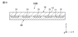
- a wiring board 100B according to a third embodiment will be described with reference to Fig. 9 and Fig. 10.
- Fig. 9 is a plan view of the wiring board according to the third embodiment.
- Fig. 10 is a cross-sectional view taken along line X-X in Fig. 9.
- the wiring board 100B according to the third embodiment differs from the wiring board 100 according to the first embodiment in that an insulating layer 40 is provided.
- At least a portion of the first wiring 31 arranged on the first main surface 11 of the first substrate 10 is covered with an insulating layer 40.
- the first main surface 11 located between two adjacent first wirings 31 is also covered with the insulating layer 40.
- the insulating layer 40 When viewed from the thickness direction (Z direction) of the first substrate, the insulating layer 40 may extend along the X direction.
- the thickness of the insulating layer 40 is not particularly limited, but in order to suppress moisture penetration and achieve a thin structure, the thickness of the insulating layer 40 is preferably 40 ⁇ m or more and 80 ⁇ m or less.
- the material of the insulating layer 40 may be an insulating material based on acrylic oligomer or urethane acrylate.
- the insulating layer 40 is preferably a low water-absorbent insulating resin such as silicone resin, acrylic resin, olefin resin, modified urethane resin, vinyl chloride resin, polyester, polyamide, polyolefin, polyethylene, or polypropylene, or a low water-absorbent insulating layer containing a paraxylylene-based polymer.
- the insulating layer 40 is in the form of a sheet or film.
- a wiring board 100C according to a fourth embodiment will be described with reference to Fig. 11.
- Fig. 11 is a cross-sectional view of the wiring board according to the fourth embodiment.
- Fig. 11 corresponds to Fig. 10 of the third embodiment.
- the wiring board 100C according to the fourth embodiment differs from the wiring board 100 according to the first embodiment in that a covering layer 60 is provided.
- the first wiring 31 is covered with a coating layer 60.
- the first main surface 11 located between two adjacent first wirings 31 is also covered with the coating layer 60. This makes it possible to prevent moisture from entering the first wiring 31 from the outside.
- the coating layer 60 extends along the X direction.
- the thickness of the coating layer 60 is preferably 40 ⁇ m or more and 80 ⁇ m or less.
- the material of the covering layer 60 is not particularly limited, and may be, for example, a laminate.
- the laminate material may be, for example, an adhesive-type stretchable film, a highly adhesive crystal gel, or an ultra-thin PDMS sheet.
- Such a material improves the biocompatibility of the wiring board.
- the covering layer 60 has an affinity for living tissue, which reduces the possibility of the living body having a foreign body reaction or rejection reaction.
- the covering layer 60 is in the form of a film or sheet.
- FIG. 12 is a cross-sectional view of the wiring board according to the fifth embodiment.
- Fig. 12 corresponds to Fig. 10 of the third embodiment.
- the wiring board 100D according to the fifth embodiment is different from the wiring board 100 according to the first embodiment in that a thermoplastic sheet 50 is provided.
- the first wiring 31 is covered with a thermoplastic sheet 50, which contacts and adheres to the first main surface 11.
- the first main surface 11 located between adjacent first wirings 31 is also covered with the thermoplastic sheet 50. This prevents moisture from penetrating into the first wiring 31.
- the connection strength between the thermoplastic sheet 50 and the first wiring 31 is improved, allowing the first wiring 31 to be firmly fixed to the first substrate 10.
- the thermoplastic sheet 50 can be made of a material such as a thermoplastic resin. More specifically, it can be made of a thermoplastic polyurethane (TPU), a polyethylene (PE), or the like.
- the thermoplastic sheet 50 is in the form of a sheet or film. From the viewpoint of making the wiring board thinner overall, it is preferable that the thickness of the thermoplastic sheet 50 is 160 ⁇ m or less.
- the materials of the thermoplastic sheet 50 and the first substrate 10 may be the same or different.
- thermoplastic sheet 50A covers the first wiring 31, contacts and adheres to the first main surface 11, and further contacts and adheres to the second wiring 32. This increases the connection strength between the thermoplastic sheet 50A and the second wiring 32.
- thermoplastic sheet 50A may be spaced apart from the second wiring 32.
- a gap may be provided between the thermoplastic sheet 50A and the second wiring 32. More specifically, in the area where the first substrate 10 and the second substrate 20 overlap, the edge of the thermoplastic sheet 50A and the edge of the second wiring 32 may be spaced apart via a gap.
- thermoplastic sheet 50A being provided so as to be spaced apart from the connection portion between the first wiring 31 and the second wiring 32.
- an edge 81 in the extension direction of the first substrate 10 is positioned further outward in the extension direction of the first substrate 10 than an edge 82 in the extension direction of the first wiring 31.
- the first substrate 10 has another edge 85 on the opposite side of the extension direction to the edge 81, and the edge 81 is farther away from the other edge 85 than the edge 82. This prevents the first wiring 31 from being exposed from the first substrate 10, and the first substrate 10 can protect the first wiring 31.
- FIG. 14 is a cross-sectional view of a second modified example of the wiring board according to the fifth embodiment.
- the thermoplastic sheet 50B covers the first wiring 31, contacts and adheres to the first main surface 11, and further contacts and adheres to the second wiring 32 and the second base material 20. That is, the thermoplastic sheet 50B is arranged so as to be sandwiched between the first substrate 10 and the second substrate 20, and may be in contact with and adhered to both the first main surface 11 and the second main surface 21. This increases the connection strength between the thermoplastic sheet 50B and the second substrate 20. Furthermore, the adhesive strength between the first substrate 10 and the second substrate 20 may also be improved.
- the thermoplastic sheet 50B may have the same thickness as the second wiring 32. More specifically, the thermoplastic sheet 50B may have the same thickness as the second wiring 32 at least in the region where the first substrate 10 and the second substrate 20 overlap. At this time, the thermoplastic sheet 50B may not be in contact with the second wiring 32.
- the thickness of the thermoplastic sheet may be smaller than that of the second wiring 32 as shown in FIG. 13, or may be equal to that of the second wiring 32 as shown in FIG. 14. Alternatively, in order to place more importance on protecting the wiring, the thermoplastic sheet may have a thickness larger than that of the second wiring 32.
- the thickness of the thermoplastic sheet does not necessarily have to be uniform across the X direction.
- the thermoplastic sheet may have a smaller thickness in the region where the first substrate 10 and the second substrate 20 overlap than in other regions. More specifically, the thermoplastic sheet may have a smaller thickness in a portion proximal to the connection point between the first wiring 31 and the second wiring 32. That is, the thermoplastic sheet may have a smaller thickness in the region where multiple components are overlapped. This makes it possible to reduce the overall thickness of the wiring board in the region where multiple components are overlapped, thereby making it possible to make the wiring board thinner.
- thermoplastic sheet as described above may also be provided on the second substrate 20 that is overlaid on the first substrate 10. That is, the second substrate may include a thermoplastic sheet that covers the second wiring 32 and is in contact with and adhered to the second main surface 21. The thermoplastic sheet that covers the second wiring 32 may be in contact with and adhered to the first wiring 31. Alternatively, the thermoplastic sheet that covers the second wiring 32 may be separated from the first wiring 31. By covering each of the first wiring 31 and the second wiring 32 with a thermoplastic sheet, it is possible to obtain the effects of suppressing the intrusion of moisture into each wiring and improving the adhesive strength between the wiring and the base material.
- a wiring having a portion covered by a covering member such as the above-mentioned thermoplastic sheet, insulating layer, and/or covering layer does not necessarily have to have a uniform thickness.
- the overlapping portion of the wiring that overlaps with the covering member and the non-overlapping portion that does not overlap with the covering member may have different thicknesses.
- Such "overlapping portion” and “non-overlapping portion” can also be referred to as “covered portion” and “non-covered portion”, respectively.
- the wiring may have a smaller thickness in the overlapping portion than in the non-overlapping portion.
- the thickness of the wiring in the non-overlapping portion may be larger than the thickness of the wiring in the overlapping portion.
- the wiring is suitably protected by the covering member and can be more suitably adhered to the substrate, so that it is possible for the wiring to have a relatively small thickness. Having a small thickness of the wiring allows the wiring board to be made thinner.
- a wiring board 100E according to a sixth embodiment will be described with reference to Fig. 15.
- Fig. 15 is a cross-sectional view of the wiring board according to the sixth embodiment.
- the wiring board 100E according to the sixth embodiment is different from the wiring board 100B according to the third embodiment in that a covering layer 60 is further provided.
- the insulating layer 40 is covered with a covering layer 60.
- the material of the covering layer 60 is different from that of the insulating layer 40.
- the covering layer 60 extends along the X direction.
- the covering layer 60 is bonded to the insulating layer 40 via an adhesive.
- the covering layer 60 may also be bonded to the second substrate 20.
- the covering layer 60 may be, for example, a laminate.
- the material of the covering layer 60 is, for example, a hydrocarbon-based material, a urethane gel tape, a silicone elastomer, or the like. Such a material improves the biocompatibility of the wiring board.
- the covering layer 60 has an affinity for living tissue, and this can suppress the occurrence of a foreign body reaction or rejection reaction in the living body.
- the thickness of the covering layer 60 is preferably 20 ⁇ m or more and 80 ⁇ m or less.
- a wiring board 100F according to a seventh embodiment will be described with reference to Fig. 16 and Fig. 17.
- Fig. 16 is a plan view of the wiring board according to the seventh embodiment.
- Fig. 17 is a cross-sectional view taken along line XVII-XVII of Fig. 16.
- the wiring board 100F according to the seventh embodiment differs from the wiring board 100E according to the sixth embodiment in that an electronic component 90 and a resist 80 are provided.
- the resist 80 is disposed between the first substrate 10 and the second substrate 20 in the thickness direction (Z direction) of the first substrate. Specifically, the resist 80 is in contact with the first main surface 11 and the second main surface 21. Furthermore, the resist 80 is not present between the first main surface 11 and the first wiring 31, and the resist 80 is not present between the second main surface 21 and the second wiring 32.
- the resist may be disposed so as to be in contact with both the second wiring 32 disposed on the second main surface 21 and the first main surface 11. This allows the space between the first substrate 10 and the second substrate 20 to be filled with the resist 80, thereby preventing foreign matter from adhering to the first wiring 31 from the outside.
- the material of the resist 80 is not particularly limited, but may be, for example, a liquid epoxy solder resist, an alkaline development type solder resist, a UV curing type solder resist, or a heat curing type solder resist.
- the shape of the resist 80 is not particularly limited, but may be a film or sheet.
- the electronic component 90 is electrically connected to the second wiring 32.
- the electronic component 90 may be connected to one or more second wirings 32.
- the type of electronic component 90 but it may be, for example, an inductor or a capacitor.
- the number of electronic components 90 A large number of electronic components 90 may be mounted as necessary.
- a wiring board 100G according to an eighth embodiment will be described with reference to Fig. 18.
- Fig. 18 is a cross-sectional view of the wiring board according to the eighth embodiment.
- Fig. 18 corresponds to Fig. 4 of the first embodiment.
- the wiring board 100G according to the eighth embodiment is different from the wiring board 100 according to the first embodiment in the width of the first wiring 31A.
- the first wiring 31A and the second wiring 32 are in contact.
- the width L3 of the first wiring 31A is smaller than the width L1 of the second wiring 32. This increases the contact area between the first substrate 10 and the second wiring 32, improving the connection strength between the first substrate 10 and the second wiring 32.
- the width L3 of the first wiring 31A is the size in the direction perpendicular to the extension direction of the first wiring 31A when viewed from the Z direction.
- the width L3 of the first wiring 31A is the size of the first wiring 31A in the Y direction.
- the width L3 of the first wiring 31A is the maximum value of the width of the first wiring 31A. If it is difficult to measure the maximum value of the first wiring 31A, the average width of the first wiring 31A is taken as L3.
- the width L1 of the second wiring 32 is the size in the direction perpendicular to the extension direction of the second wiring 32 when viewed from the Z direction.
- the width L1 of the second wiring 32 is the size of the second wiring 32 in the Y direction.
- the width L1 of the second wiring 32 is the maximum width of the second wiring 32. If it is difficult to measure the maximum width of the second wiring 32, the average width of the second wiring 32 is taken as L1.
- the average value refers to the average value of the measurement values obtained by measuring the width of one first wiring 31A at three different points along the extension direction (X direction) in the area where the first substrate 10 and the second substrate 20 overlap.
- a wiring board 100H according to a ninth embodiment will be described with reference to Fig. 19.
- Fig. 19 is a cross-sectional view of the wiring board according to the ninth embodiment.
- Fig. 19 corresponds to Fig. 4 of the first embodiment.
- the wiring board 100H according to the ninth embodiment is different from the wiring board 100 according to the first embodiment in the shape of the third main surface 12.
- the first substrate 10 is in contact with and adhered to the second substrate 20.
- the first substrate 10 covers the first wiring 31 and the second wiring 32.
- the third main surface 12 of the first substrate 10, which is located on the opposite side of the first main surface in contact with the first wiring 31, has an uneven shape. This increases the surface area of the third main surface 12 of the first substrate 10, improving the heat dissipation of the first wiring 31.
- the heater comes into contact with the convex parts of the third main surface 12, and heat can be concentrated on the convex parts of the first substrate 10. This allows for rapid thermocompression bonding.
- the third main surface 12 when viewed from the Z direction, has a convex shape in the region where it overlaps with the first wiring 31, and a concave shape in the region between two adjacent first wirings 31.
- the third main surface 12 is formed along the first wiring 31 and the second main surface 21 between the two adjacent first wirings 31.
- Fig. 20 is a cross-sectional view of the wiring board according to the tenth embodiment.
- Fig. 20 corresponds to Fig. 4 of the first embodiment.
- the wiring board 100I according to the tenth embodiment is different from the wiring board 100 according to the first embodiment in the size and number of second wirings 32A.
- the first wirings 31 and one second wiring 32A are electrically connected to face each other in the thickness direction (Z direction) of the first substrate. That is, among the first wirings 31 arranged on the first main surface 11, at least two first wirings 31 may be electrically connected to the same second wiring 32A. Specifically, the width of the second wiring 32A in the Y direction is larger than the width of the first wiring 31 in the Y direction, and two or more first wirings 31 are connected to one second wiring 32A.
- the second wiring 32A may extend in the Y direction so as to be mutually connected to each of the first wirings 31 arranged in parallel with each other in the Y direction.
- the adjacent first wirings 31 are spaced apart from each other. This reduces the number of second wirings 32A relative to the first wirings 31, and increases the design freedom of the wiring board 100I.
- a portion of the first substrate 10 is disposed between each of the multiple adjacent first wirings 31 and contacts the second wiring 32A. This ensures insulation between the adjacent first wirings 31.
- the form of connection between the first wiring 31 and the second wiring 32A is not particularly limited. For example, multiple second wirings and one first wiring may be electrically connected. In this case, it is preferable that the second substrate 20 is made of the same material as the first substrate 10.
Landscapes
- Engineering & Computer Science (AREA)
- Microelectronics & Electronic Packaging (AREA)
- Structure Of Printed Boards (AREA)
Abstract
配線基板は、 第1主面を有する第1基材と、 第2主面を有する第2基材と、 前記第1主面に配置された第1配線と、 前記第2主面に配置された第2配線と を備え、 前記第1主面と前記第2主面とは接触し、前記第1基材と前記第2基材とは接続され、 前記第1配線と前記第2配線とは、前記第1基材の厚み方向に対向して電気的に接続される。
Description
本開示は、配線基板に関する。
従来、配線基板として、特開平7-94861号公報(特許文献1)に記載されたものがある。この配線基板は、第1基材と第2基材に加熱接着性の絶縁レジストを形成し、絶縁レジスト上に電極パターンを形成し、各基材の電極パターンを対向させて圧接し、圧接状態で電極パターン周辺のレジストを加熱接着したものである。このように、配線基板は、第1基材と第2基材との間に2層の絶縁レジストを有する。第1基材と第2基材とは、2層の絶縁レジストを介して、接続されている。
ところで、前記従来のような配線基板では、第1基材と第2基材の間に2層の絶縁レジストが存在するため、配線基板が厚くなる問題がある。
そこで、本開示の目的は、薄型化を図ることができる配線基板を提供することにある。
上記目的を達成するために、本発明の一態様に係る配線基板は、
第1主面を有する第1基材と、
第2主面を有する第2基材と、
前記第1主面に配置された第1配線と、
前記第2主面に配置された第2配線と
を備え、
前記第1主面と前記第2主面とが接触し、第1基材と第2基材とが接続され、
前記第1配線と前記第2配線とは、前記第1基材の厚み方向に対向して電気的に接続される。
第1主面を有する第1基材と、
第2主面を有する第2基材と、
前記第1主面に配置された第1配線と、
前記第2主面に配置された第2配線と
を備え、
前記第1主面と前記第2主面とが接触し、第1基材と第2基材とが接続され、
前記第1配線と前記第2配線とは、前記第1基材の厚み方向に対向して電気的に接続される。
本発明の一態様に係る配線基板によれば、薄型化を図ることができる。
以下、本発明の実施形態について、図面を用いて詳細に説明する。各々の実施形態では、その実施形態以前に説明した点と異なる点について主に説明する。特に、同様の構成による同様の作用効果については実施形態ごとには逐次言及しない。以下の実施形態における構成要素のうち、独立請求項に記載されていない構成要素については、任意の構成要素として説明される。また、図面に示される構成要素の大きさ及び大きさの比は、必ずしも厳密ではない。また各図において、実質的に同一の構成に対しては同一の符号を付しており、重複する説明は省略または簡略化する場合がある。
[第1実施形態]
(構造)
図1、図2、図3、図4および図5を参照しながら、第1実施形態に係る配線基板の構造について、説明する。図1は、本発明の第1実施形態に係る配線基板の分解斜視図である。図2は、配線基板の分解平面図である。図3は、配線基板の平面図である。図4は、図3のIV-IV断面図である。図5は、図3のV-V断面図である。
(構造)
図1、図2、図3、図4および図5を参照しながら、第1実施形態に係る配線基板の構造について、説明する。図1は、本発明の第1実施形態に係る配線基板の分解斜視図である。図2は、配線基板の分解平面図である。図3は、配線基板の平面図である。図4は、図3のIV-IV断面図である。図5は、図3のV-V断面図である。
本明細書の図面では、第1基材の厚み方向に平行で、かつ第1基材の第1主面から第3主面に向かう方向を矢印Zで示している。厚み方向は、順Z方向および逆Z方向の何れの方向をも含みうる。この実施形態では、第2基材の厚み方向もZ方向に平行となる。また、第1基材の延在方向に平行で、かつ第1基材のうちの第2基材から離れている位置から第2基材に近い位置に向かう方向を矢印Xで示している。第1基材の延在方向は、順X方向および逆X方向の何れの方向をも含みうる。この実施形態では、第1配線、第2基材および第2配線の延在方向もX方向に平行となる。X方向とZ方向は直交し、X方向およびZ方向に直交する方向をY方向とする。X,Y,Zの順に並べたとき、右手系を構成する。
配線基板100は第1主面11を有する第1基材10と、第2主面21を有する第2基材20と、第1主面11に配置された第1配線31と、第2主面21に配置された第2配線32と、を備えている。配線基板100は、例えば、プリント基板、またはフレキシブル基板との回路接続に用いられる。
第1基材10は、伸縮性を有する樹脂材料から構成されるフィルム材などの支持材である。第1基材10の形状はシート状またはフィルム状である。第1基材10は、互いに反対側に位置する第1主面11および第3主面12を有する。
第1基材10は、第1主面11に凹部14を有する(図4参照)。凹部14は、Z方向から見て、第1基材10と第2基材20が重なる領域70に少なくとも存在する。凹部14は、第1主面11にて、第1基材がZ方向(すなわち、第1基材10の厚み方向)に凹んだ部分に相当する。そのため、凹部14の内面は、第1主面11の凹みを形成する面と解することもできる。第1主面11は、凹部14の内面と、凹部14以外の平坦面とから構成されてよい。凹部14は、X方向に沿って延在していてよい。凹部14は、複数存在することができる。複数の凹部14の各々は、Y方向に沿って互いに平行に並んで配置されていてよい。第3主面12は、本実施形態では露出面である。
第1基材10の材料としては、例えば、熱可塑性樹脂などが挙げられる。具体的には、第1基材10の材料は、伸縮性を有する樹脂材料であり、例えば、スチレン樹脂、オレフィン樹脂、エポキシ樹脂、ウレタン樹脂、アクリル樹脂及び/又はシリコーン樹脂を含んでいる。より具体的には、熱可塑性ポリウレタン(Thermoplastic polyurethane:TPU、)、ポリエチレン(polyethene:PE)などが挙げられる。また、樹脂材料は、軟化点を有する事が好ましい。具体的には、軟化点が90度以上であることがより好ましい。それにより、第1基材10の第1主面11と第2基材20の第2主面21とが接触しやすくなる。
第1基材10は伸縮性を有する。第1基材10が伸縮性を有することで、配線基板100の使用時の伸縮における破断の危険性を低減することができる。第1基材10の厚さは特に限定されないが、生体に貼り付けた際に生体表面の伸縮を阻害しない観点からは、160μm以下であることが好ましく、80μm以下であることがより好ましい。また、第1基材10の厚さは、40μm以上であることが好ましい。
第2基材20は、互いに反対側に位置する第2主面21および第4主面22を有する。Z方向から見て、第2基材20のX方向の端部は、第1基材10のX方向の端部と重なる。より具体的には、第2基材20の逆X方向の端部は、第1基材10の順X方向の端部と重なる。第2主面21は、第1主面11と対向する。本実施形態では、第4主面22は、露出面である。なお、第4主面22は、露出していなくてもよい。
本実施形態では、第2基材20は、第1基材10と異なる基材であり、例えば、リジット基板やフレキシブル基板などである。リジット基板としては、例えば、ガラス繊維製の布を重ねた物に、エポキシ樹脂を含浸させ製造したガラスエポキシ基板が使用される。フレキシブル基板としては、例えば、耐熱性に優れたプラスチックであるポリイミドが使用される。
第2基材20の第2主面21と第1基材10の第1主面11とが接触することで、第1基材10と第2基材20とが接続される(図3参照)。それにより、配線基板100の薄型化を図ることができる。つまり、第1基材10と第2基材20とは、絶縁レジストを必要とせずに直接接触して接続されるので、従来の絶縁レジストを介した接触と比較して、絶縁レジストの厚みの分だけデバイス全体の厚みを薄くできる。また、絶縁レジストが不要となるので、絶縁レジストの印刷も不要になる。それにより、配線基板の製造コストや工数を削減できる。
好ましくは、第1基材10の第1主面11と第2基材20の第2主面21とは、互いに接触して接着されている。接着とは、例えば、熱圧着、溶着、融着などである。第1基材10と第2基材20が重なる領域70において、第1主面11と第2主面21の少なくとも一部が、接触し接着されていればよい。
ここで、接着とは、20Nの引張力に耐えることができることである。第1基材10と第2基材20における接着強さの評価はJIS K 6849に基づいて行うことができる。接触して接着とは、第1基材10の第1主面11と第2基材20の第2主面21とが接着剤などの他の部材を介さないで直接に貼り付いていることをいう。
したがって、第1主面11と第2主面21との面接触によって第1基材10と第2基材20とが接触するので、第1基材10と第2基材20との接続強度が向上する。なお、第1主面と第2主面が接触するための方法は特に限定されないが、例えば、第1基材10と第2基材20の側面に別の部材を介して第1基材10と第2基材20が接続されて、第1主面と第2主面が接触してもよい。
第1主面11と第2主面21とが接触する領域において、第1主面11と第2主面21との界面の位置が判別できない場合、第1主面11における第2主面21と重ならない非重複面から、当該非重複面と同一面となるように延長した延長面と、第1主面11と第2主面21が接触する領域とが重なる部分を界面とする。図5に示すように、第1主面11と第2主面21とが接触しない領域に位置する第1主面11の平坦面11a(非重複面)の延長面11bを、第1主面11と第2主面21との界面とする。言い換えれば、延長面11bとは、第1基材10と第2基材20との接触領域において平坦面11aと実質的に同一面となる面である。なお、延長面は仮想の面であることはいうまでもない。以降の実施形態についても同様である。
第1配線31は、第1基材10の第1主面11に配置されている。少なくとも第1基材10と第2基材20が重なる領域70において、第1配線31は、一方向に延在する形状を有する。具体的に述べると、第1配線31は、X方向に沿って延在していてよい。第1配線31は、複数存在し得る。複数の第1配線31が、Y方向に沿って互いに平行に並んで配置されていてよい。なお、第1配線31の形状は特に限定されない。
第1配線31は導電性材料で形成される。導電性材料には、例えば、銀、銅、ニッケルなどの金属箔を用いてもよく、または銀、銅、ニッケルなどの金属粉とエポキシ樹脂及びシリコーン樹脂などのエラストマ系樹脂とからなる混合物を用いてもよい。第1配線31は、好ましくは伸縮性を有する。
第1配線31は、第1基材10の第1凹部14に配置されている。第1配線31は、第1主面11にて、第1凹部14に嵌め込まれるように配されていてよい。これは、第1配線31が第1凹部14内に配置され、第1凹部14に沿って延在すると解することもできる。また、1つの第1配線31は、1つの第1凹部14に配置されている。すなわち、複数の第1配線31の各々は、複数の第1凹部14の各々に、別個に配され得る。このような構造によれば、Y方向にて互いに隣接する2つの第1配線31の間に第1基材10が存在することになる。これにより、互いに隣接する2つの第1配線31の間の絶縁性を確保することができる。配線基板全体の薄型化を図る観点から、第1配線31の厚みは、30μm以下であることが好ましい。
第2配線32は、第1基材10の第1凹部14に配置されている。少なくとも、第1基材10と第2基材20が重なる領域70において、第2配線32は一方向に延在する形状を有する。具体的に言うと、第2配線32はX方向に沿って延在していてよい。第2配線32は、複数存在し得る。複数の第2配線32は、Y方向にて、互いに平行に並んで配置されていてよい。なお、第2配線32の形状は特に限定しない。
第2配線32は導電性材料で形成される。導電性材料には、例えば、銀、銅、ニッケルなどの金属箔を用いてもよく、銀、銅、ニッケルなどの金属粉とエポキシ樹脂及びシリコーン樹脂などのエラストマ系樹脂とからなる混合物を用いてもよい。好ましくは、第2配線32は伸縮性を有する。
第1配線31と第2配線32とは、Z方向(第1基材の厚み方向)に対向して電気的に接続される。具体的に述べると、第1配線31と第2配線32とは、直接に接触して電気的に接続される。なお、第1配線31と第2配線32とは、第1配線31と第2配線32の間に配置された導電性部材を介して、電気的に接続されていてもよい。
好ましくは、第2配線32は、第1凹部14に配された第1配線31と接触していてよい。この際、断面視にて、第1配線31と第2配線32とは、第1凹部14にて互いに接触していてよい。一方で、第1主面11と第2主面21とは、第1主面11の平坦面にて接触していてよい(図4参照)。このような構造において、断面視にて、第1配線31と第2配線32の間における界面と、第1主面11と第2主面21との間における界面とは、互いに異なる平面上に位置する。第1配線31および第2配線32の界面と、第1基材10および第2基材20の界面とが断面視にて互いに異なる平面上に位置することで、第1基材10と第2基材20の接着面における剥離に対する強度が向上し得る。
図4に示すように、第1基材10と第2基材20が重なる領域70において、複数の第2配線32は、Y方向に並んで配置される。好ましくは、第2配線32の幅L1と、Y方向に隣り合う2つの第2配線32の間の幅L2との比率L1/L2は、1以上20以下である。L1/L2の比率が20以下であると、隣り合う2つの第2配線32の間の絶縁性を好適に確保できる。また、第1主面11と第2主面21との接触面積を十分に確保することで、第1基材10と第2基材20との接続強度が向上される。L1/L2の比率が1以上であると、より大きな第2配線32を確保でき、第2配線32の電気抵抗を小さくできる。なお、複数の第2配線32のうち、少なくともY方向にて互いに隣り合う2つの第2配線32において上記構成を満たしていればよく、好ましくは、全ての第2配線32において上記構成を満たしていればよい。同様に、第1配線31の幅および隣り合う2つの第1配線31間の距離についても、上記の関係を満たすことがより好ましい。
ここで、第2配線32の幅L1は、Z方向からみて第2配線32の延在する方向に直交する方向の大きさである。つまり、第2配線32の幅L1は、第2配線32のY方向の大きさである。第2配線32の幅L1は、第2配線32の幅の最大値とする。第2配線32における最大値の測定が困難である場合、第2配線32の幅の平均値をL1とする。第1配線31の幅は、第2配線32の幅L1と同じであってよい。
同様に、Y方向にて互いに隣り合う2つの第2配線32の間の幅L2は、Y方向にて互いに隣り合う2つの第2配線32の間のY方向における最短距離とする。第2配線32の間のY方向における最短距離の測定が困難である場合、Y方向に隣り合う2つの第2配線32の間の幅の平均値をL2とする。
平均値とは、第1基材10と第2基材20が重なる領域において、一つの第2配線32に対し延在方向(X方向)に沿って異なる3か所の幅を測定して得られた測定値の平均値をいう。
図3に示すように、第1基材の厚み方向(Z方向)から見て、第1基材10と第2基材20とが重なる領域70において、複数の第2配線32は、Y方向に並んで配置される。領域70において、第2配線32が存在する領域71(以下、第1領域71という)の面積S1と、Y方向に隣り合う2つの第2配線32の間の領域72(以下、第2領域72という)の面積S2との比率S1/S2は、好ましくは1以上20以下である。
ここで、第1領域71とは、Z方向から見て、第1基材10と第2基材20との重なる領域70における1つの第2配線32の領域である。第2領域72とは、Z方向から見て、Y方向に隣り合う2つの第1領域71の間の領域である。図3では、便宜上、第1領域71および第2領域72をハッチングで示す。第1領域71および第2領域72は、それぞれ、矩形の形状を有してよい。X方向において、第1領域71と第2領域72の長さは同じである。なお、第1領域71及び第2領域72の形状は、矩形に限定されない。
比率S1/S2が20以下であることで、隣り合う2つの第2配線32の間の絶縁性を好適に確保できる。また、第1主面11と第2主面21との接触面積を確保できる。それにより、第1基材10と第2基材20の接続強度が向上される。また、比率S1/S2が1以上であることで、より大きな第2配線32を配置できるため、第2配線32の電気抵抗を小さくできる。
好ましくは、Z方向において、第1配線31から第1基材10の第3主面12までの距離D1は、第1基材10と第2基材20との界面から第1基材10の第3主面12までの距離D2より小さい(図4参照)。距離D1は、第1配線31と第3主面12の間の最小値をいい、距離D2は、第1基材10と第2基材20との界面と第3主面12の間の最小値をいう。これにより、第1基材10の第3主面12の形状をより平坦にすることができる。好ましくは、距離D2は、第1配線31の厚みと第2配線32の厚みの合計以上である。また、距離D1を小さくすることで、Z方向から見て第1配線31と重なる部分の第1基材10の厚みを小さくできる。Z方向から見て、配線と重なる部分の基材は、基材の伸縮性の低下が予測される。上記構造によれば、伸縮性の低下が予測される部分の基材の厚みを小さくすることができるので、第1基材10が伸縮性を有する場合、第1基材10の伸縮性が良好となる。
(製造方法)
次に、図6Aと図6Bを用いて例示的な配線基板100の製造方法について説明する。
次に、図6Aと図6Bを用いて例示的な配線基板100の製造方法について説明する。
図6Aに示すように、第1配線31を第1基材10の第1主面11に複数形成する。同様に、第2配線32を第2基材20の第2主面21に複数形成する。Z方向(すなわち、基材の厚み方向)において、第1配線31と第2配線32とが対向するように、第1基材10と第2基材20を重ねる。そして、互いに重ねられた第1基材10と第2基材20とを熱圧着する。これは、例えば、第1基材10の第3主面12にヒータを押し当てることで実施されてよい。
図6Bに示すように、ヒータによる加圧および加熱により、Y方向にて互いに隣接する複数の配線同士の間の空間など、配線が配置されていない空間に第1基材10が流動する。流動した第1基材10は、第1配線31と第2配線32を覆いつつ、第2基材20に接触する。これにより、第1基材10の第1主面11と第2基材20の第2主面21が熱圧着し、第1配線31と第2配線32は第1凹部14に配置される。第1基材10は、軟化点を有するので、第1基材10が加熱された際に流動しやすくなり、第2基材20と接触しやすくなる。つまり、軟化点を有する第1基材10は、熱圧着に好適である。また、第1基材10は熱可塑性を有するので、同様に、熱圧着に好適となる。なお、熱圧着の方法は特に限定されず、例えば第2基材20の第4主面22に他のヒータを押し当てるようにしてもよい。
[第2実施形態]
(構造)
次に、図7を参照して、第2実施形態について説明する。図7は、第2実施形態に係る配線基板100Aの断面図である。図7は、第1実施形態の図4に対応する。第2実施形態に係る配線基板100Aは、第1実施形態に係る配線基板100と比較して、第2基材20Aの構造が相違する。
(構造)
次に、図7を参照して、第2実施形態について説明する。図7は、第2実施形態に係る配線基板100Aの断面図である。図7は、第1実施形態の図4に対応する。第2実施形態に係る配線基板100Aは、第1実施形態に係る配線基板100と比較して、第2基材20Aの構造が相違する。
図7に示すように、第2基材20Aは、互いに反対側に位置する第2主面21および第4主面22を有する。第1基材10は、第1主面11に第1凹部14を有し、第2基材20Aは、第2主面21に第2凹部24を有する。第1配線31は、第1凹部24に配置され、第2配線32は、第2凹部24に配置される。1つの第1配線31は、1つの第1凹部14に配置されている。1つの第2配線32は、1つの第2凹部24に配置されている。
上記構成によれば、第1配線31が第1凹部14に配置されるので、Y方向にて互いに隣り合う2つの第1配線31の間に第1基材10が存在することになる。これにより、隣接する2つの第1配線31の間の絶縁性が確保されることができる。同様に、第2配線32が第2凹部24に配置されるので、Y方向に隣り合う2つの第2配線32の間に第2基材20Aが存在することになる。それにより、隣接する2つの第2配線32の間の絶縁性を確保することができる。
上述の構造では、第1基材10と第2基材20Aのそれぞれに凹部14,24を設け、各凹部14,24に配線31,32を配置している。それにより、第1基材10および第2基材20Aの厚みをより減じることができるため、より配線基板の薄型化を図ることができる。
第2基材20Aは、第1基材10と同様の伸縮性を有する基材であり、例えば、熱可塑性樹脂である。具体的に述べると、熱可塑性樹脂としては、熱可塑性ポリウレタン(Thermoplastic polyurethane:TPU)、ポリエチレン(polyethene:PE)などが挙げられる。熱可塑性樹脂は軟化点を有し、例えば、軟化点が90度以上である。第2基材20Aの形状は、シート状またはフィルム状であることが好ましい。第2基材20Aの厚さは特に限定されないが、生体に貼り付けた際に、生体表面の伸縮を阻害しない観点から、160μm以下であることが好ましく、80μm以下であることがより好ましい。また、第2基材20Aの厚さは、40μm以上であることが好ましい。第2基材20Aの材料は、第1基材と同じ材料であることが好ましい。第1基材10と同じ材料であることで、配線基板全体の伸縮量を均一に近づけることができる。なお、第1基材10と第2基材20Aとは異なる材料であってもよい。
また、本実施形態によれば、第1実施形態と同様に、第2基材20Aについても、第2配線32と第2基材20Aの第4主面22との距離を小さくできる。つまり、Z方向から見て第2配線32と重なる部分の第2基材20Aの厚みを小さくできるので、第2基材20Aが伸縮性を有する場合、第2基材20Aの伸縮性が良好となる。
好ましくは、第1主面11と第2主面21とは接触し接着されている。好ましくは、第1配線31と第2配線32とは、Z方向に対向して接触している。好ましくは、断面視にて、第1配線31と第2配線32の間における界面と、第1主面11と第2主面21との間における界面とは、同一の平面上に位置する。すなわち、配線同士の接触面と、基材同士の接触面とが、同一平面上に位置する。界面が一致することで、第1基材10側と第2基材20A側の伸縮量を均一に近づけることができる。なお、第1配線31と第2配線32の間における界面と、第1主面11と第2主面21との間における界面とは、同一の平面上に位置してなくてもよい。
(製造方法)
次に、図8Aと図8Bを用いて配線基板100Aの製造方法について説明する。
次に、図8Aと図8Bを用いて配線基板100Aの製造方法について説明する。
図8Aに示すように、複数の第1配線31を第1基材10の第1主面11に形成する。同様に、複数の第2配線32を第2基材20Aの第2主面21に形成する。Z方向において、第1配線31と第2配線32とが対向するように、第1基材10と第2基材20Aを重ねる。そして、第1基材10の第3主面12と第2基材20Aの第4主面22のそれぞれにヒータを押し当てて、ヒータにより第1基材10および第2基材20Aを加熱する。
図8Bに示すように、ヒータによる加圧および加熱により、第1基材10は、互いに隣り合う2つの第1配線31の間に流動する。また、第2基材20Aは、互いに隣り合う2つの第2配線32の間に流動する。流動した第1基材10と第2基材20Aは、第1配線31と第2配線32を覆いつつ、互いに接触する。これにより、第1基材10の第1主面11と第2基材20Aの第2主面21とが熱圧着する。第1配線31は第1凹部14に配置され、第2配線32は第2凹部24に配置される。第1基材10と第2基材20Aは軟化点を有するので、第1基材10と第2基材20Aが加熱された際に流動しやすくなり、互いに接触しやすくなる。つまり、熱圧着に好適となる。また、第1基材10と第2基材20Aは熱可塑性を有するので、同様に熱圧着に好適となる。
[第3実施形態]
次に、図9と図10を参照して第3実施形態に係る配線基板100Bを説明する。図9は、第3実施形態に係る配線基板の平面図である。図10は図9のX-X断面図である。第3実施形態に係る配線基板100Bは、第1実施形態に係る配線基板100と比較し、絶縁層40が設けられている点が相違する。
次に、図9と図10を参照して第3実施形態に係る配線基板100Bを説明する。図9は、第3実施形態に係る配線基板の平面図である。図10は図9のX-X断面図である。第3実施形態に係る配線基板100Bは、第1実施形態に係る配線基板100と比較し、絶縁層40が設けられている点が相違する。
図10に示すように、第1基材10の第1主面11に配置された第1配線31の少なくとも一部は、絶縁層40に覆われている。好ましくは、互いに隣り合う2つの第1配線31の間に位置する第1主面11上も、絶縁層40に覆われている。第1配線31が絶縁層40に覆われることで、第1配線31に対する外部からの水分の侵入が抑制され、さらに、第1配線31に対する短絡も防止され得る。
第1基材の厚み方向(Z方向)から見て、絶縁層40は、X方向に沿って延在していてよい。絶縁層40の厚みは特に限定しないが、水分侵入抑制及び薄型化を図るために、絶縁層40の厚みは40μm以上で、80μm以下であることが好ましい。
絶縁層40の材料は、アクリルオリゴマーもしくはウレタンアクリレート主剤の絶縁材料であってよい。絶縁層40は、例えば、シリコーン樹脂、アクリル樹脂、オレフィン樹脂、変性ウレタン樹脂、塩化ビニル樹脂、ポリエステル、ポリアミド、ポリオレフィン、ポリエチレン、ポリプロピレンなどの低吸水性絶縁樹脂、又は、パラキシリレン系ポリマーなどを含む低吸水性絶縁層などであることが好ましい。絶縁層40の形状は、シート状またはフィルム状である。
[第4実施形態]
次に、図11を参照して、第4実施形態に係る配線基板100Cを説明する。図11は、第4実施形態に係る配線基板の断面図である。図11は、第3実施形態の図10に対応する。第4実施形態に係る配線基板100Cは、第1実施形態に係る配線基板100と比較し、被覆層60が設けられている点が相違する。
次に、図11を参照して、第4実施形態に係る配線基板100Cを説明する。図11は、第4実施形態に係る配線基板の断面図である。図11は、第3実施形態の図10に対応する。第4実施形態に係る配線基板100Cは、第1実施形態に係る配線基板100と比較し、被覆層60が設けられている点が相違する。
図11に示すように、第1配線31の少なくとも一部が被覆層60に覆われている。好ましくは、互いに隣り合う2つの第1配線31の間に位置する第1主面11も、被覆層60に覆われている。それにより、第1配線31において、外部からの水分の侵入を抑制できる。第1基材の厚み方向(Z方向)から見て、被覆層60は、X方向に沿って延在している。被覆層60の厚みは特に限定しないが、水分の侵入抑制および薄型化の両立の観点から、被覆層60の厚みは40μm以上80μm以下であることが好ましい。
被覆層60の材料は特に限定しないが、例えば、ラミネートなどでもよい。ラミネートの材料は、例えば、粘着剤タイプの伸縮性フィルム、高粘着クリスタルゲル、超極薄PDMSシートである。このような材料によれば、配線基板の生体適合性が向上される。例えば、被覆層60が生体に接触するように配線基板100Cを使用する際、被覆層60が生体組織に対して親和性を有することで、生体が異物反応や拒絶反応などを起こす可能性を低減できる。被覆層60の形状は、フィルム状またはシート状である。
[第5実施形態]
図12を参照して、第5実施形態に係る配線基板100Dを説明する。図12は、第5実施形態に係る配線基板の断面図である。図12は、第3実施形態の図10に対応する。第5実施形態に係る配線基板100Dは、第1実施形態に係る配線基板100と比較して、熱可塑性シート50が設けられている点が相違する。
図12を参照して、第5実施形態に係る配線基板100Dを説明する。図12は、第5実施形態に係る配線基板の断面図である。図12は、第3実施形態の図10に対応する。第5実施形態に係る配線基板100Dは、第1実施形態に係る配線基板100と比較して、熱可塑性シート50が設けられている点が相違する。
図12に示すように、第1配線31の少なくとも一部は、熱可塑性シート50に覆われ、熱可塑性シート50は、第1主面11に接触して接着する。具体的に言うと、隣り合う第1配線31の間に位置する第1主面11も、熱可塑性シート50に覆われている。これにより、第1配線31への水分の侵入が抑制される。さらに、熱可塑性シート50と第1配線31との接続強度が向上し、第1配線31を第1基材10に対して強固に固定することができる。
熱可塑性シート50の材料としては、熱可塑性樹脂などが挙げられる。具体的に述べると、熱可塑性ポリウレタン(Thermoplastic polyurethane:TPU)、ポリエチレン(polyethene:PE)などである。熱可塑性シート50の形状は、シート状またはフィルム状である。配線基板の全体的な薄型化を図る観点から、熱可塑性シート50の厚みは160μm以下であるのが好ましい。熱可塑性シート50と第1基材10の材料は、同じであってもよく、異なっていてもよい。
[第1変形例]
図13は、第5実施形態に係る配線基板の第1変形例の断面図である。図13に示すように、熱可塑性シート50Aは、第1配線31を覆い、第1主面11に接触して接着し、さらに、第2配線32に接触して接着する。それにより、熱可塑性シート50Aと第2配線32との接続強度が強くなる。
図13は、第5実施形態に係る配線基板の第1変形例の断面図である。図13に示すように、熱可塑性シート50Aは、第1配線31を覆い、第1主面11に接触して接着し、さらに、第2配線32に接触して接着する。それにより、熱可塑性シート50Aと第2配線32との接続強度が強くなる。
代替的には、熱可塑性シート50Aは、第2配線32と離隔していてもよい。図13に示す断面視にて、熱可塑性シート50Aと第2配線32との間には、空隙が設けられていてよい。より具体的には、第1基材10と第2基材20と重なる領域において、熱可塑性シート50Aの端縁と第2配線32の端縁とは、空隙を介して離隔していてよい。これは、熱可塑性シート50Aが、第1配線31と第2配線32との接続部分と離隔するように設けられていると解することもできる。かかる構造によれば、熱圧着時などにおける熱に起因して熱可塑性シート50Aが変形または流動し、第1配線31と第2配線32との接続部分にまで及ぶことを抑制できる。つまり、熱可塑性シート50Aと第2配線32とを離隔することで、熱可塑性シート50Aが配線同士の接続を阻害する可能性が低減されるため、配線同士の接続信頼性がより向上し得る。
好ましくは、第1基材の厚み方向(Z方向)から見て、第1基材10と第2基材20と重なる領域において、第1基材10の延在方向の端縁81は、第1配線31の延在方向の端縁82よりも、第1基材10の延在方向の外側に位置する。具体的に述べると、第1基材10は、端縁81とは延在方向の反対側に他方の端縁85を有し、端縁81は、端縁82よりも他方の端縁85から離れている。それにより、第1配線31は第1基材10から露出することを防止し、第1基材10により第1配線31を保護することができる。
[第2変形例]
図14は、第5実施形態に係る配線基板の第2変形例の断面図である。図14に示すように、熱可塑性シート50Bは、第1配線31を覆い、第1主面11に接触して接着し、さらに、第2配線32と第2基材20に接触して接着する。すなわち、熱可塑性シート50Bは、第1基板10と第2基板20との間にて挟持されるように配置され、第1主面11および第2主面21の双方と接触および接着していてよい。これにより、熱可塑性シート50Bと第2基材20との接続強度が強くなる。さらに、第1基材10と第2基材20との接着強度も向上し得る。このような構造において、熱可塑性シート50Bは、第2配線32と同じ厚みを有していてよい。より具体的には、熱可塑性シート50Bは、少なくとも、第1基板10と第2基板20とが重なる領域において、第2配線32と同じ厚みを有していてよい。なお、このとき、熱可塑性シート50Bは、第2配線32に接触しなくてもよい。
図14は、第5実施形態に係る配線基板の第2変形例の断面図である。図14に示すように、熱可塑性シート50Bは、第1配線31を覆い、第1主面11に接触して接着し、さらに、第2配線32と第2基材20に接触して接着する。すなわち、熱可塑性シート50Bは、第1基板10と第2基板20との間にて挟持されるように配置され、第1主面11および第2主面21の双方と接触および接着していてよい。これにより、熱可塑性シート50Bと第2基材20との接続強度が強くなる。さらに、第1基材10と第2基材20との接着強度も向上し得る。このような構造において、熱可塑性シート50Bは、第2配線32と同じ厚みを有していてよい。より具体的には、熱可塑性シート50Bは、少なくとも、第1基板10と第2基板20とが重なる領域において、第2配線32と同じ厚みを有していてよい。なお、このとき、熱可塑性シート50Bは、第2配線32に接触しなくてもよい。
熱可塑性シートの厚みは、図13に示すように第2配線32より小さくてもよく、あるいは図14に示すように第2配線32と同等であってもよい。代替的には、配線の保護をより重視する観点から、熱可塑性シートは、第2配線32よりも大きい厚みを有していてもよい。
また、図13および14に示す断面視にて、熱可塑性シートの厚みは、X方向にわたって必ずしも均一でなくてよい。例えば、熱可塑性シートは、第1基板10と第2基板20とが重なる領域において、その他の領域より小さい厚みを有していてよい。より具体的には、熱可塑性シートは、第1配線31と第2配線32との接続箇所に近位する部分にて、より小さい厚みを有していてよい。すなわち、複数の部材が重ねられる領域にて、熱可塑性シートはより小さい厚みを有していてよい。これにより、複数の部材が重ねられる領域における配線基板全体の厚みを減じることができるため、配線基板の薄型化が可能となる。
また、上述のような熱可塑性シートは、第1基板10と重ねられる第2基板20にも設けられていてよい。すなわち、第2基板は、第2配線32を覆い、第2主面21に接触して接着する熱可塑性シートを備えていてよい。第2配線32を覆う熱可塑性シートは、第1配線31と接触および接着していてよい。代替的には、第2配線32を覆う熱可塑性シートは、第1配線31とは離隔していてもよい。第1配線31および第2配線32のそれぞれが熱可塑性シートによって覆われることで、各配線への水分の侵入の抑制、および配線と基材との接着強度の向上の効果を得ることができる。
上述した熱可塑性シート、絶縁層、および/または被覆層などの被覆部材によって覆われた部分を有する配線は、必ずしも均一な厚みを有していなくてよい。配線は、被覆部材と重なる重なり部分と、被覆部材と重ならない非重なり部分とで互いに異なる厚みを有していてよい。かかる“重なり部分”および“非重なり部分”は、それぞれ“被覆部分”および“非被覆部分”と称すこともできる。例えば、配線は、重なり部分において、非重なり部分より小さい厚みを有していてよい。換言すれば、非重なり部分における配線の厚みは、重なり部分における配線の厚みより大きくてよい。重なり部分においては、配線は、被覆部材によって好適に保護され、基材に対してより好適に密着することができるため、比較的小さい厚みを有することが可能となる。配線が小さい厚みを有することで、配線基板をより薄型化することが可能となる。
[第6実施形態]
次に、図15を参照して、第6実施形態に係る配線基板100Eを説明する。図15は、第6実施形態に係る配線基板の断面図である。第6実施形態に係る配線基板100Eは、第3実施形態に係る配線基板100Bと比較し、さらに被覆層60が設けられている点が相違する。
次に、図15を参照して、第6実施形態に係る配線基板100Eを説明する。図15は、第6実施形態に係る配線基板の断面図である。第6実施形態に係る配線基板100Eは、第3実施形態に係る配線基板100Bと比較し、さらに被覆層60が設けられている点が相違する。
図15に示すように、絶縁層40は、被覆層60に覆われている。被覆層60の材料は、絶縁層40と異なる材料である。第1基材の厚み方向(Z方向)から見て、被覆層60がX方向に沿って延在している。
それにより、絶縁層40の劣化を防止でき、絶縁層40に含まれる成分の漏出を防止できる。好ましくは、被覆層60は接着剤を介して絶縁層40と接着する。また被覆層60が第2基材20と接着してもよい。
被覆層60は、例えば、ラミネートなどでもよい。被覆層60の材料は、例えば炭化水素系、ウレタンゲルテープ、シリコーンエラストマーなど材料である。このような材料によれば、配線基板の生体適合性が向上される。例えば、被覆層60が生体に接触するように配線基板100Eを使用する際、被覆層60が生体組織に対して親和性を有することで、生体が異物反応や拒絶反応などを起こすことを抑制できる。また、生体適合性の向上および配線基板の薄型化の両立の観点から、被覆層60の厚みは20μm以上80μm以下であることが好ましい。
[第7実施形態]
次に、図16と図17を参照して、第7実施形態に係る配線基板100Fを説明する。図16は、第7実施形態に係る配線基板の平面図である。図17は、図16のXVII-XVII断面図である。実施形態7に係る配線基板100Fは、実施形態6に係る配線基板100Eと比較して、電子部品90とレジスト80とが設けられる点が相違する。
次に、図16と図17を参照して、第7実施形態に係る配線基板100Fを説明する。図16は、第7実施形態に係る配線基板の平面図である。図17は、図16のXVII-XVII断面図である。実施形態7に係る配線基板100Fは、実施形態6に係る配線基板100Eと比較して、電子部品90とレジスト80とが設けられる点が相違する。
図16と図17に示すように、第1基材の厚み方向(Z方向)における第1基材10と第2基材20との間にレジスト80が配置される。具体的に述べると、レジスト80は第1主面11と第2主面21と接触している。さらに、レジスト80は第1主面11と第1配線31の間に存在せず、かつレジスト80は第2主面21と第2配線32の間に存在しない。例えば、レジストは、第2主面21上に配された第2配線32および第1主面11の双方に接触するように配置されていてよい。それにより、第1基材10と第2基材20の間の空間をレジスト80で埋めることができるため、外部から第1配線31に異物が付着することを防止することができる。
レジスト80の材料は特に限定しないが、例えば、液状エポキシソルダーレジスト、アルカリ現像型ソルダーレジスト、UV硬化型ソルダーレジスト、熱硬化型ソルダーレジストなどの材料である。レジスト80の形状は特に限定しないが、フィルム状またはシート状でもよい。
電子部品90は、第2配線32と電気的に接続されている。電子部品90と電気的に接続する第2配線32の本数は特に限定しないが、一本または複数の第2配線32と接続してよい。電子部品90の種類は特に限定しないが、例えば、インダクター、コンデンサなどである。電子部品90の数は特に限定しない。必要に応じて、多数の電子部品90を搭載してもよい。
[第8実施形態]
次に、図18を参照して、第8実施形態に係る配線基板100Gを説明する。図18は、第8実施形態に係る配線基板の断面図である。図18は、第1実施形態の図4に対応する。第8実施形態に係る配線基板100Gは、第1実施形態に係る配線基板100と比較し、第1配線31Aの幅が相違する。
次に、図18を参照して、第8実施形態に係る配線基板100Gを説明する。図18は、第8実施形態に係る配線基板の断面図である。図18は、第1実施形態の図4に対応する。第8実施形態に係る配線基板100Gは、第1実施形態に係る配線基板100と比較し、第1配線31Aの幅が相違する。
図18に示すように、第1配線31Aと第2配線32とは接触する。第1基材10と第2基材20が重なる領域70において、第1配線31Aの幅L3は第2配線32の幅L1より小さい。それにより、第1基材10と第2配線32との接触面積が大きくなり、第1基材10と第2配線32との接続強度が向上される。
ここで、第1配線31Aの幅L3は、Z方向から見て第1配線31Aの延在する方向に直交する方向の大きさである。つまり、第1配線31Aの幅L3は、第1配線31AのY方向の大きさである。第1配線31Aの幅L3は、第1配線31Aの幅の最大値とする。第1配線31Aにおける最大値の測定が困難である場合、第1配線31Aの幅の平均値をL3とする。
ここで、第2配線32の幅L1は、Z方向からみて第2配線32の延在する方向に直交する方向の大きさである。つまり、第2配線32の幅L1は、第2配線32のY方向の大きさである。第2配線32の幅L1は、第2配線32の幅の最大値とする。第2配線32における最大値の測定が困難である場合、第2配線32の幅の平均値をL1とする。
平均値とは、第1基材10と第2基材20が重なる領域において、一つの第1配線31Aについて、延在方向(X方向)に沿って異なる3か所の幅を測定して得られた測定値の平均値をいう。
[第9実施形態]
次に、図19を参照して、第9実施形態に係る配線基板100Hを説明する。図19は、第9実施形態に係る配線基板の断面図である。図19は、第1実施形態の図4に対応する。第9実施形態に係る配線基板100Hは、第1実施形態に係る配線基板100と比較して、第3主面12の形状が相違する。
次に、図19を参照して、第9実施形態に係る配線基板100Hを説明する。図19は、第9実施形態に係る配線基板の断面図である。図19は、第1実施形態の図4に対応する。第9実施形態に係る配線基板100Hは、第1実施形態に係る配線基板100と比較して、第3主面12の形状が相違する。
図19に示すように、第1基材10は、第2基材20と接触して接着する。第1基材10は、第1配線31と第2配線32を覆っている。第1基材10において、第1配線31と接触している第1主面の反対側に位置する第3主面12の形状は、凹凸状である。これにより、第1基材10の第3主面12の表面積が広くなり、第1配線31の放熱性が向上される。また、配線基板の製造時における第1基材10と第2基材20の熱圧着に際して、ヒータと第3主面12の凸部とが接触し、第1基材10の凸部に集中して熱を与えることができる。これにより、迅速に熱圧着を行うことができる。
図19に示すように、第3主面12は、Z方向からみて、第1配線31と重なる領域に凸形状を有し、互いに隣り合う2つの第1配線31の間の領域に凹形状を有する。つまり、第3主面12は、第1配線31と、互いに隣り合う2つの第1配線31の間の第2主面21とに沿って形成されている。
[第10実施形態]
次に、図20を参照して、第10実施形態に係る配線基板100Iを説明する。図20は、第10実施形態に係る配線基板の断面図である。図20は、第1実施形態の図4に対応する。第10実施形態に係る配線基板100Iは、第1実施形態に係る配線基板100と比較して、第2配線32Aの大きさおよび数が相違する。
次に、図20を参照して、第10実施形態に係る配線基板100Iを説明する。図20は、第10実施形態に係る配線基板の断面図である。図20は、第1実施形態の図4に対応する。第10実施形態に係る配線基板100Iは、第1実施形態に係る配線基板100と比較して、第2配線32Aの大きさおよび数が相違する。
図20に示すように、複数の第1配線31と1つの第2配線32Aとは、第1基材の厚み方向(Z方向)に対向して電気的に接続される。つまり、第1主面11に配される複数の第1配線31のうち、少なくとも2つの第1配線31が同一の第2配線32Aと互いに電気的に接続されていてよい。具体的に述べると、第2配線32AのY方向の幅は、第1配線31のY方向の幅よりも大きく、1つの第2配線32Aに2つ以上の第1配線31が接続される。第2配線32Aは、Y方向にて互いに並列する複数の第1配線31の各々と相互に接続するように、Y方向にわたって延在していてよい。隣り合う複数の第1配線31は、互いに離隔している。これにより、複数の第1配線31に対する第2配線32Aの数量が削減され、配線基板100Iの設計自由度が高くなる。
第1基材10の一部は、隣り合う複数の第1配線31のそれぞれの間に配置され、第2配線32Aに接触する。それにより、隣り合う第1配線31の間の絶縁性が確保される。なお、第1配線31と第2配線32Aとの接続の形態は特に限定しない。例えば、複数の第2配線と1つの第1配線とを電気的に接続してもよい。このとき、第2基材20が第1基材10と同じ材料であることが好ましい。
なお、本開示は上述の実施形態に限定されず、本開示の要旨を逸脱しない範囲で設計変更可能である。例えば、第1から第10実施形態のそれぞれの特徴点を様々に組み合わせてもよい。
100、100A、100B、100C、100D、100E、100F、100G、100H、100I 配線基板
10 第1基材
11 第1主面
11a 平坦面
11b 延長面
12 第3主面
20、20A 第2基材
21 第2主面
22 第4主面
31 31A 第1配線
32 32A 第2配線
40 絶縁層
50、50A、50B 熱可塑性シート
60 被覆層
70 第1基材と第2基材が重なる領域
71 第2配線の領域
72 隣り合う2つの第2配線の間の領域
80 レジスト
81 第1基材の端縁
82 第1配線の端縁
85 他方の端縁
90 電子部品
L1 第2配線の幅
L2 第2配線間の幅
L3 第1配線の幅
D1 第1配線から第3主面までの距離
D2 第1基材と第2基材との界面から第3主面までの距離
X 第1基材の延在方向
Z 第1基材の厚み方向
10 第1基材
11 第1主面
11a 平坦面
11b 延長面
12 第3主面
20、20A 第2基材
21 第2主面
22 第4主面
31 31A 第1配線
32 32A 第2配線
40 絶縁層
50、50A、50B 熱可塑性シート
60 被覆層
70 第1基材と第2基材が重なる領域
71 第2配線の領域
72 隣り合う2つの第2配線の間の領域
80 レジスト
81 第1基材の端縁
82 第1配線の端縁
85 他方の端縁
90 電子部品
L1 第2配線の幅
L2 第2配線間の幅
L3 第1配線の幅
D1 第1配線から第3主面までの距離
D2 第1基材と第2基材との界面から第3主面までの距離
X 第1基材の延在方向
Z 第1基材の厚み方向
Claims (19)
- 第1主面を有する第1基材と、
第2主面を有する第2基材と、
前記第1主面に配置された第1配線と、
前記第2主面に配置された第2配線と
を備え、
前記第1主面と前記第2主面とは接触し、前記第1基材と前記第2基材とは接続され、
前記第1配線と前記第2配線とは、前記第1基材の厚み方向に対向して電気的に接続される、配線基板。 - 前記第1基材は、前記第1主面に第1凹部を有し、
前記第1配線と前記第2配線は、前記第1凹部に配置される、請求項1に記載の配線基板。 - 前記第1配線と前記第2配線とは、前記厚み方向に対向して接触し、
前記第1配線と前記第2配線の間の界面と、前記第1主面と前記第2主面の間の界面とは、異なる平面上に位置する、請求項1または2に記載の配線基板。 - 前記第1基材は第3主面を有し、
前記厚み方向において、前記第1配線から前記第3主面までの距離は、前記第1基材と前記第2基材の界面から前記第3主面までの距離より小さい、請求項1から3の何れか一つに記載の配線基板。 - 前記第1基材は、前記第1主面に第1凹部を有し、前記第2基材は、前記第2主面に第2凹部を有し、前記第1配線は、前記第1凹部に配置され、前記第2配線は、前記第2凹部に配置される、請求項1に記載の配線基板。
- さらに、前記第1配線の少なくとも一部を覆う絶縁層を備える、請求項1から5の何れか一つに記載の配線基板。
- さらに、前記第1配線の少なくとも一部を覆う被覆層を備える、請求項1から5の何れか一つに記載の配線基板。
- さらに、前記第1配線の少なくとも一部を覆い、前記第1主面に接触して接着する熱可塑性シートを備える、請求項1から5の何れか一つに記載の配線基板。
- 前記熱可塑性シートが、さらに、前記第2配線と接触して接着する、請求項8に記載の配線基板。
- 前記熱可塑性シートは、さらに、前記第2主面に接触して接着する、請求項8または9に記載の配線基板。
- さらに、前記絶縁層の少なくとも一部を覆う被覆層を備え、前記被覆層の材料は前記絶縁層の材料と異なる、請求項6に記載の配線基板。
- 前記厚み方向からみて前記第1基材と前記第2基材と重なる領域において、前記第1基材の延在方向の端縁は、前記第1配線の延在方向の端縁よりも、前記第1基材の延在方向の外側に位置する、請求項1から11の何れか一つに記載の配線基板。
- さらに、前記厚み方向における前記第1基材と前記第2基材との間に配置されるレジストを備える、請求項1から12の何れか一つに記載の配線基板。
- 前記第1基材と前記第2基材が重なる領域において、前記第2配線は複数並んで配置され、前記第2配線の幅L1と、隣り合う2つの前記第2配線の間の幅L2との比率L1/L2は、1以上、20以下である、請求項1から13の何れか一つに記載の配線基板。
- 前記第1基材と前記第2基材が重なる領域において、前記第1配線の幅L3は、前記第2配線の幅L1よりも小さい、請求項1から14の何れか一つに記載の配線基板。
- 前記第1基材は第3主面を有し、
前記第3主面の形状は、凹凸状である、請求項1から15の何れか一つに記載の配線基板。 - 複数の前記第1配線と1つの前記第2配線とは、前記厚み方向に対向して電気的に接続される、請求項1から16の何れか一つに記載の配線基板。
- 前記第1基材の一部は、隣り合う前記複数の第1配線のそれぞれの間に配置され、前記第2配線に接触する、請求項17に記載の配線基板。
- 第1基材及び第2基材の内の少なくとも第1基材は、軟化点を有する請求項1から18の何れか一つに記載の配線基板。
Priority Applications (2)
| Application Number | Priority Date | Filing Date | Title |
|---|---|---|---|
| JP2024549941A JP7747227B2 (ja) | 2022-09-30 | 2023-09-04 | 配線基板 |
| US19/089,550 US20250227846A1 (en) | 2022-09-30 | 2025-03-25 | Wiring board |
Applications Claiming Priority (2)
| Application Number | Priority Date | Filing Date | Title |
|---|---|---|---|
| US202263411770P | 2022-09-30 | 2022-09-30 | |
| US63/411,770 | 2022-09-30 |
Related Child Applications (1)
| Application Number | Title | Priority Date | Filing Date |
|---|---|---|---|
| US19/089,550 Continuation US20250227846A1 (en) | 2022-09-30 | 2025-03-25 | Wiring board |
Publications (1)
| Publication Number | Publication Date |
|---|---|
| WO2024070518A1 true WO2024070518A1 (ja) | 2024-04-04 |
Family
ID=90477330
Family Applications (1)
| Application Number | Title | Priority Date | Filing Date |
|---|---|---|---|
| PCT/JP2023/032240 Ceased WO2024070518A1 (ja) | 2022-09-30 | 2023-09-04 | 配線基板 |
Country Status (3)
| Country | Link |
|---|---|
| US (1) | US20250227846A1 (ja) |
| JP (1) | JP7747227B2 (ja) |
| WO (1) | WO2024070518A1 (ja) |
Citations (9)
| Publication number | Priority date | Publication date | Assignee | Title |
|---|---|---|---|---|
| JP2000049423A (ja) * | 1998-07-30 | 2000-02-18 | Sony Chem Corp | フレキシブル基板 |
| JP2001111209A (ja) * | 1999-07-30 | 2001-04-20 | Denso Corp | プリント配線板の接続方法および接続構造 |
| JP2001223465A (ja) * | 1999-11-30 | 2001-08-17 | Denso Corp | プリント配線基板の接続方法及び接続構造 |
| JP2002050863A (ja) * | 2000-08-04 | 2002-02-15 | Denso Corp | プリント配線基板の接続方法 |
| JP2004247403A (ja) * | 2003-02-12 | 2004-09-02 | Denso Wave Inc | 半田付け装置、半田付け方法、基板接続装置及び基板接続方法 |
| JP2004311578A (ja) * | 2003-04-03 | 2004-11-04 | Fujikura Ltd | プリント配線基板の接合方法並びに複合プリント配線基板 |
| JP2005045066A (ja) * | 2003-07-23 | 2005-02-17 | Matsushita Electric Ind Co Ltd | 電気的接続構造およびその製造方法 |
| JP2015023059A (ja) * | 2013-07-16 | 2015-02-02 | 住友電工プリントサーキット株式会社 | フレキシブルプリント配線板の接続構造、フレキシブルプリント配線板及びその製造方法 |
| JP2017195230A (ja) * | 2016-04-18 | 2017-10-26 | 日本メクトロン株式会社 | 伸縮性配線基板、及び、伸縮性配線基板の製造方法 |
-
2023
- 2023-09-04 JP JP2024549941A patent/JP7747227B2/ja active Active
- 2023-09-04 WO PCT/JP2023/032240 patent/WO2024070518A1/ja not_active Ceased
-
2025
- 2025-03-25 US US19/089,550 patent/US20250227846A1/en active Pending
Patent Citations (9)
| Publication number | Priority date | Publication date | Assignee | Title |
|---|---|---|---|---|
| JP2000049423A (ja) * | 1998-07-30 | 2000-02-18 | Sony Chem Corp | フレキシブル基板 |
| JP2001111209A (ja) * | 1999-07-30 | 2001-04-20 | Denso Corp | プリント配線板の接続方法および接続構造 |
| JP2001223465A (ja) * | 1999-11-30 | 2001-08-17 | Denso Corp | プリント配線基板の接続方法及び接続構造 |
| JP2002050863A (ja) * | 2000-08-04 | 2002-02-15 | Denso Corp | プリント配線基板の接続方法 |
| JP2004247403A (ja) * | 2003-02-12 | 2004-09-02 | Denso Wave Inc | 半田付け装置、半田付け方法、基板接続装置及び基板接続方法 |
| JP2004311578A (ja) * | 2003-04-03 | 2004-11-04 | Fujikura Ltd | プリント配線基板の接合方法並びに複合プリント配線基板 |
| JP2005045066A (ja) * | 2003-07-23 | 2005-02-17 | Matsushita Electric Ind Co Ltd | 電気的接続構造およびその製造方法 |
| JP2015023059A (ja) * | 2013-07-16 | 2015-02-02 | 住友電工プリントサーキット株式会社 | フレキシブルプリント配線板の接続構造、フレキシブルプリント配線板及びその製造方法 |
| JP2017195230A (ja) * | 2016-04-18 | 2017-10-26 | 日本メクトロン株式会社 | 伸縮性配線基板、及び、伸縮性配線基板の製造方法 |
Also Published As
| Publication number | Publication date |
|---|---|
| JP7747227B2 (ja) | 2025-10-01 |
| US20250227846A1 (en) | 2025-07-10 |
| JPWO2024070518A1 (ja) | 2024-04-04 |
Similar Documents
| Publication | Publication Date | Title |
|---|---|---|
| US20220377886A1 (en) | Laminated body and method for manufacturing the same | |
| US10847695B2 (en) | Light emitting device | |
| US11622442B2 (en) | Circuit member joint structure and circuit member joining method | |
| JP5672091B2 (ja) | 多層基板 | |
| JP7747227B2 (ja) | 配線基板 | |
| JP2013135172A (ja) | プリント配線板及びプリント配線板の接続構造 | |
| US20250210505A1 (en) | Stretchable device | |
| JP6683264B2 (ja) | 電子機器 | |
| US20170090108A1 (en) | Planar illumination device | |
| US12451268B2 (en) | Electric contact terminal | |
| TWI855712B (zh) | 顯示裝置 | |
| WO2023171464A1 (ja) | 伸縮性デバイス | |
| JP5006162B2 (ja) | 電気接続部材 | |
| WO2024070591A1 (ja) | 伸縮性デバイス | |
| JP7036213B2 (ja) | フレキシブル基板及びその製造方法、並びに電子機器 | |
| US12341233B2 (en) | Signal transmission line | |
| US12349596B2 (en) | Vibration device | |
| JP6460280B2 (ja) | 部品実装基板 | |
| WO2025033274A1 (ja) | 伸縮性デバイス | |
| JP4085609B2 (ja) | 端子付き配線基板 | |
| WO2024122492A1 (ja) | 半導体装置 | |
| WO2025249367A1 (ja) | 伸縮性デバイス | |
| JP2024007723A (ja) | 圧電振動ユニット | |
| TW202338448A (zh) | 電子裝置 | |
| JP4303558B2 (ja) | 接続装置の製造方法 |
Legal Events
| Date | Code | Title | Description |
|---|---|---|---|
| 121 | Ep: the epo has been informed by wipo that ep was designated in this application |
Ref document number: 23871758 Country of ref document: EP Kind code of ref document: A1 |
|
| WWE | Wipo information: entry into national phase |
Ref document number: 2024549941 Country of ref document: JP |
|
| NENP | Non-entry into the national phase |
Ref country code: DE |
|
| 122 | Ep: pct application non-entry in european phase |
Ref document number: 23871758 Country of ref document: EP Kind code of ref document: A1 |