WO2024029385A1 - 半導体装置 - Google Patents
半導体装置 Download PDFInfo
- Publication number
- WO2024029385A1 WO2024029385A1 PCT/JP2023/027007 JP2023027007W WO2024029385A1 WO 2024029385 A1 WO2024029385 A1 WO 2024029385A1 JP 2023027007 W JP2023027007 W JP 2023027007W WO 2024029385 A1 WO2024029385 A1 WO 2024029385A1
- Authority
- WO
- WIPO (PCT)
- Prior art keywords
- metal layer
- conductive member
- semiconductor device
- layer
- semiconductor
- Prior art date
- Legal status (The legal status is an assumption and is not a legal conclusion. Google has not performed a legal analysis and makes no representation as to the accuracy of the status listed.)
- Ceased
Links
Images


Classifications
-
- H—ELECTRICITY
- H10—SEMICONDUCTOR DEVICES; ELECTRIC SOLID-STATE DEVICES NOT OTHERWISE PROVIDED FOR
- H10W—GENERIC PACKAGES, INTERCONNECTIONS, CONNECTORS OR OTHER CONSTRUCTIONAL DETAILS OF DEVICES COVERED BY CLASS H10
- H10W40/00—Arrangements for thermal protection or thermal control
- H10W40/10—Arrangements for heating
-
- H—ELECTRICITY
- H10—SEMICONDUCTOR DEVICES; ELECTRIC SOLID-STATE DEVICES NOT OTHERWISE PROVIDED FOR
- H10W—GENERIC PACKAGES, INTERCONNECTIONS, CONNECTORS OR OTHER CONSTRUCTIONAL DETAILS OF DEVICES COVERED BY CLASS H10
- H10W40/00—Arrangements for thermal protection or thermal control
- H10W40/20—Arrangements for cooling
- H10W40/25—Arrangements for cooling characterised by their materials
-
- H—ELECTRICITY
- H10—SEMICONDUCTOR DEVICES; ELECTRIC SOLID-STATE DEVICES NOT OTHERWISE PROVIDED FOR
- H10W—GENERIC PACKAGES, INTERCONNECTIONS, CONNECTORS OR OTHER CONSTRUCTIONAL DETAILS OF DEVICES COVERED BY CLASS H10
- H10W70/00—Package substrates; Interposers; Redistribution layers [RDL]
- H10W70/40—Leadframes
- H10W70/456—Materials
- H10W70/457—Materials of metallic layers on leadframes
-
- H—ELECTRICITY
- H10—SEMICONDUCTOR DEVICES; ELECTRIC SOLID-STATE DEVICES NOT OTHERWISE PROVIDED FOR
- H10W—GENERIC PACKAGES, INTERCONNECTIONS, CONNECTORS OR OTHER CONSTRUCTIONAL DETAILS OF DEVICES COVERED BY CLASS H10
- H10W70/00—Package substrates; Interposers; Redistribution layers [RDL]
- H10W70/40—Leadframes
- H10W70/481—Leadframes for devices being provided for in groups H10D8/00 - H10D48/00
-
- H—ELECTRICITY
- H10—SEMICONDUCTOR DEVICES; ELECTRIC SOLID-STATE DEVICES NOT OTHERWISE PROVIDED FOR
- H10W—GENERIC PACKAGES, INTERCONNECTIONS, CONNECTORS OR OTHER CONSTRUCTIONAL DETAILS OF DEVICES COVERED BY CLASS H10
- H10W72/00—Interconnections or connectors in packages
- H10W72/071—Connecting or disconnecting
- H10W72/073—Connecting or disconnecting of die-attach connectors
-
- H—ELECTRICITY
- H10—SEMICONDUCTOR DEVICES; ELECTRIC SOLID-STATE DEVICES NOT OTHERWISE PROVIDED FOR
- H10W—GENERIC PACKAGES, INTERCONNECTIONS, CONNECTORS OR OTHER CONSTRUCTIONAL DETAILS OF DEVICES COVERED BY CLASS H10
- H10W72/00—Interconnections or connectors in packages
- H10W72/30—Die-attach connectors
-
- H—ELECTRICITY
- H10—SEMICONDUCTOR DEVICES; ELECTRIC SOLID-STATE DEVICES NOT OTHERWISE PROVIDED FOR
- H10W—GENERIC PACKAGES, INTERCONNECTIONS, CONNECTORS OR OTHER CONSTRUCTIONAL DETAILS OF DEVICES COVERED BY CLASS H10
- H10W74/00—Encapsulations, e.g. protective coatings
- H10W74/10—Encapsulations, e.g. protective coatings characterised by their shape or disposition
- H10W74/111—Encapsulations, e.g. protective coatings characterised by their shape or disposition the semiconductor body being completely enclosed
-
- H—ELECTRICITY
- H10—SEMICONDUCTOR DEVICES; ELECTRIC SOLID-STATE DEVICES NOT OTHERWISE PROVIDED FOR
- H10W—GENERIC PACKAGES, INTERCONNECTIONS, CONNECTORS OR OTHER CONSTRUCTIONAL DETAILS OF DEVICES COVERED BY CLASS H10
- H10W74/00—Encapsulations, e.g. protective coatings
- H10W74/40—Encapsulations, e.g. protective coatings characterised by their materials
-
- H—ELECTRICITY
- H10—SEMICONDUCTOR DEVICES; ELECTRIC SOLID-STATE DEVICES NOT OTHERWISE PROVIDED FOR
- H10W—GENERIC PACKAGES, INTERCONNECTIONS, CONNECTORS OR OTHER CONSTRUCTIONAL DETAILS OF DEVICES COVERED BY CLASS H10
- H10W76/00—Containers; Fillings or auxiliary members therefor; Seals
- H10W76/10—Containers or parts thereof
- H10W76/12—Containers or parts thereof characterised by their shape
- H10W76/13—Containers comprising a conductive base serving as an interconnection
- H10W76/138—Containers comprising a conductive base serving as an interconnection having another interconnection being formed by a cover plate parallel to the conductive base, e.g. sandwich type
-
- H—ELECTRICITY
- H10—SEMICONDUCTOR DEVICES; ELECTRIC SOLID-STATE DEVICES NOT OTHERWISE PROVIDED FOR
- H10W—GENERIC PACKAGES, INTERCONNECTIONS, CONNECTORS OR OTHER CONSTRUCTIONAL DETAILS OF DEVICES COVERED BY CLASS H10
- H10W90/00—Package configurations
-
- H—ELECTRICITY
- H10—SEMICONDUCTOR DEVICES; ELECTRIC SOLID-STATE DEVICES NOT OTHERWISE PROVIDED FOR
- H10D—INORGANIC ELECTRIC SEMICONDUCTOR DEVICES
- H10D30/00—Field-effect transistors [FET]
- H10D30/60—Insulated-gate field-effect transistors [IGFET]
- H10D30/64—Double-diffused metal-oxide semiconductor [DMOS] FETs
- H10D30/66—Vertical DMOS [VDMOS] FETs
-
- H—ELECTRICITY
- H10—SEMICONDUCTOR DEVICES; ELECTRIC SOLID-STATE DEVICES NOT OTHERWISE PROVIDED FOR
- H10D—INORGANIC ELECTRIC SEMICONDUCTOR DEVICES
- H10D80/00—Assemblies of multiple devices comprising at least one device covered by this subclass
- H10D80/20—Assemblies of multiple devices comprising at least one device covered by this subclass the at least one device being covered by groups H10D1/00 - H10D48/00, e.g. assemblies comprising capacitors, power FETs or Schottky diodes
- H10D80/251—FETs covered by H10D30/00, e.g. power FETs
-
- H—ELECTRICITY
- H10—SEMICONDUCTOR DEVICES; ELECTRIC SOLID-STATE DEVICES NOT OTHERWISE PROVIDED FOR
- H10W—GENERIC PACKAGES, INTERCONNECTIONS, CONNECTORS OR OTHER CONSTRUCTIONAL DETAILS OF DEVICES COVERED BY CLASS H10
- H10W40/00—Arrangements for thermal protection or thermal control
- H10W40/20—Arrangements for cooling
- H10W40/25—Arrangements for cooling characterised by their materials
- H10W40/258—Metallic materials
-
- H—ELECTRICITY
- H10—SEMICONDUCTOR DEVICES; ELECTRIC SOLID-STATE DEVICES NOT OTHERWISE PROVIDED FOR
- H10W—GENERIC PACKAGES, INTERCONNECTIONS, CONNECTORS OR OTHER CONSTRUCTIONAL DETAILS OF DEVICES COVERED BY CLASS H10
- H10W72/00—Interconnections or connectors in packages
- H10W72/071—Connecting or disconnecting
- H10W72/073—Connecting or disconnecting of die-attach connectors
- H10W72/07351—Connecting or disconnecting of die-attach connectors characterised by changes in properties of the die-attach connectors during connecting
-
- H—ELECTRICITY
- H10—SEMICONDUCTOR DEVICES; ELECTRIC SOLID-STATE DEVICES NOT OTHERWISE PROVIDED FOR
- H10W—GENERIC PACKAGES, INTERCONNECTIONS, CONNECTORS OR OTHER CONSTRUCTIONAL DETAILS OF DEVICES COVERED BY CLASS H10
- H10W72/00—Interconnections or connectors in packages
- H10W72/50—Bond wires
- H10W72/531—Shapes of wire connectors
- H10W72/536—Shapes of wire connectors the connected ends being ball-shaped
-
- H—ELECTRICITY
- H10—SEMICONDUCTOR DEVICES; ELECTRIC SOLID-STATE DEVICES NOT OTHERWISE PROVIDED FOR
- H10W—GENERIC PACKAGES, INTERCONNECTIONS, CONNECTORS OR OTHER CONSTRUCTIONAL DETAILS OF DEVICES COVERED BY CLASS H10
- H10W72/00—Interconnections or connectors in packages
- H10W72/50—Bond wires
- H10W72/531—Shapes of wire connectors
- H10W72/5363—Shapes of wire connectors the connected ends being wedge-shaped
-
- H—ELECTRICITY
- H10—SEMICONDUCTOR DEVICES; ELECTRIC SOLID-STATE DEVICES NOT OTHERWISE PROVIDED FOR
- H10W—GENERIC PACKAGES, INTERCONNECTIONS, CONNECTORS OR OTHER CONSTRUCTIONAL DETAILS OF DEVICES COVERED BY CLASS H10
- H10W72/00—Interconnections or connectors in packages
- H10W72/50—Bond wires
- H10W72/551—Materials of bond wires
- H10W72/552—Materials of bond wires comprising metals or metalloids, e.g. silver
- H10W72/5522—Materials of bond wires comprising metals or metalloids, e.g. silver comprising gold [Au]
-
- H—ELECTRICITY
- H10—SEMICONDUCTOR DEVICES; ELECTRIC SOLID-STATE DEVICES NOT OTHERWISE PROVIDED FOR
- H10W—GENERIC PACKAGES, INTERCONNECTIONS, CONNECTORS OR OTHER CONSTRUCTIONAL DETAILS OF DEVICES COVERED BY CLASS H10
- H10W72/00—Interconnections or connectors in packages
- H10W72/50—Bond wires
- H10W72/551—Materials of bond wires
- H10W72/552—Materials of bond wires comprising metals or metalloids, e.g. silver
- H10W72/5524—Materials of bond wires comprising metals or metalloids, e.g. silver comprising aluminium [Al]
-
- H—ELECTRICITY
- H10—SEMICONDUCTOR DEVICES; ELECTRIC SOLID-STATE DEVICES NOT OTHERWISE PROVIDED FOR
- H10W—GENERIC PACKAGES, INTERCONNECTIONS, CONNECTORS OR OTHER CONSTRUCTIONAL DETAILS OF DEVICES COVERED BY CLASS H10
- H10W72/00—Interconnections or connectors in packages
- H10W72/50—Bond wires
- H10W72/551—Materials of bond wires
- H10W72/552—Materials of bond wires comprising metals or metalloids, e.g. silver
- H10W72/5525—Materials of bond wires comprising metals or metalloids, e.g. silver comprising copper [Cu]
-
- H—ELECTRICITY
- H10—SEMICONDUCTOR DEVICES; ELECTRIC SOLID-STATE DEVICES NOT OTHERWISE PROVIDED FOR
- H10W—GENERIC PACKAGES, INTERCONNECTIONS, CONNECTORS OR OTHER CONSTRUCTIONAL DETAILS OF DEVICES COVERED BY CLASS H10
- H10W72/00—Interconnections or connectors in packages
- H10W72/851—Dispositions of multiple connectors or interconnections
- H10W72/853—On the same surface
- H10W72/865—Die-attach connectors and bond wires
-
- H—ELECTRICITY
- H10—SEMICONDUCTOR DEVICES; ELECTRIC SOLID-STATE DEVICES NOT OTHERWISE PROVIDED FOR
- H10W—GENERIC PACKAGES, INTERCONNECTIONS, CONNECTORS OR OTHER CONSTRUCTIONAL DETAILS OF DEVICES COVERED BY CLASS H10
- H10W72/00—Interconnections or connectors in packages
- H10W72/851—Dispositions of multiple connectors or interconnections
- H10W72/874—On different surfaces
- H10W72/884—Die-attach connectors and bond wires
-
- H—ELECTRICITY
- H10—SEMICONDUCTOR DEVICES; ELECTRIC SOLID-STATE DEVICES NOT OTHERWISE PROVIDED FOR
- H10W—GENERIC PACKAGES, INTERCONNECTIONS, CONNECTORS OR OTHER CONSTRUCTIONAL DETAILS OF DEVICES COVERED BY CLASS H10
- H10W74/00—Encapsulations, e.g. protective coatings
- H10W74/10—Encapsulations, e.g. protective coatings characterised by their shape or disposition
- H10W74/111—Encapsulations, e.g. protective coatings characterised by their shape or disposition the semiconductor body being completely enclosed
- H10W74/114—Encapsulations, e.g. protective coatings characterised by their shape or disposition the semiconductor body being completely enclosed by a substrate and the encapsulations
-
- H—ELECTRICITY
- H10—SEMICONDUCTOR DEVICES; ELECTRIC SOLID-STATE DEVICES NOT OTHERWISE PROVIDED FOR
- H10W—GENERIC PACKAGES, INTERCONNECTIONS, CONNECTORS OR OTHER CONSTRUCTIONAL DETAILS OF DEVICES COVERED BY CLASS H10
- H10W90/00—Package configurations
- H10W90/701—Package configurations characterised by the relative positions of pads or connectors relative to package parts
- H10W90/751—Package configurations characterised by the relative positions of pads or connectors relative to package parts of bond wires
- H10W90/756—Package configurations characterised by the relative positions of pads or connectors relative to package parts of bond wires between a chip and a stacked lead frame, conducting package substrate or heat sink
Definitions
- the present disclosure relates to a semiconductor device.
- Patent Document 1 discloses an example of a conventional semiconductor device.
- the semiconductor device disclosed in the document includes a conductor, a semiconductor element, a conductive member, and a sealing resin.
- a semiconductor element is mounted on a conductor.
- a semiconductor element has an electrode.
- a conductive member is connected to this electrode via solder.
- the sealing resin covers at least a portion of each of the conductor, the semiconductor element, and the conductive member.
- the semiconductor element When a semiconductor device is in operation, the semiconductor element repeatedly generates heat. A portion of the heat generated in the semiconductor layer of the semiconductor element is radiated through the solder and the conductive member. If the amount of heat transfer (heat flux) per unit time from the semiconductor layer of the semiconductor element to the solder is not sufficient, the temperature of the semiconductor element will rise transiently. This temperature increase may impair proper operation of the semiconductor device.
- An object of the present disclosure is to provide a semiconductor device that is improved over the conventional semiconductor device.
- one object of the present disclosure is to provide a semiconductor device that can operate a semiconductor element more appropriately.
- a semiconductor device includes: a semiconductor element having a semiconductor layer and a first electrode disposed on a first side in the thickness direction of the semiconductor layer; a first conductive member, a second conductive member joined to the semiconductor element from the second side in the thickness direction, a first resin surface facing the first side in the thickness direction, and a first resin surface facing the second side in the thickness direction; A sealing resin having two resin surfaces and covering the semiconductor element and at least a portion of each of the first conductive member and the second conductive member.
- the first electrode includes a first metal layer containing a metal having higher thermal conductivity than solder.
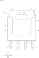
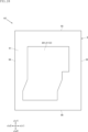
- FIG. 1 is a perspective view showing a semiconductor device according to a first embodiment of the present disclosure.
- FIG. 2 is a perspective view of main parts showing a semiconductor device according to a first embodiment of the present disclosure.
- FIG. 3 is a plan view showing a semiconductor device according to the first embodiment of the present disclosure.
- FIG. 4 is a plan view of main parts of a semiconductor device according to a first embodiment of the present disclosure.
- FIG. 5 is a bottom view showing the semiconductor device according to the first embodiment of the present disclosure.
- FIG. 6 is a bottom view of essential parts of the semiconductor device according to the first embodiment of the present disclosure.
- FIG. 7 is a side view showing the semiconductor device according to the first embodiment of the present disclosure.
- FIG. 8 is a cross-sectional view taken along line VIII-VIII in FIG. 4.
- FIG. 9 is a sectional view taken along line IX-IX in FIG. 4.
- FIG. 10 is a cross-sectional view of a main part schematically showing a first embodiment of a junction structure included in a semiconductor device of the present disclosure.
- FIG. 11 is a cross-sectional view of a main part schematically showing an example of a bonding structure included in a semiconductor device according to a first embodiment of the present disclosure.
- FIG. 12 is a cross-sectional view of a main part schematically showing another example of the bonding structure included in the semiconductor device according to the first embodiment of the present disclosure.
- FIG. 13 is a cross-sectional view of a main part schematically showing another example of a bonding structure included in the semiconductor device according to the first embodiment of the present disclosure.
- FIG. 10 is a cross-sectional view of a main part schematically showing a first embodiment of a junction structure included in a semiconductor device of the present disclosure.
- FIG. 11 is a cross-sectional view of a main part
- FIG. 14 is a cross-sectional view of main parts schematically showing another example of a bonding structure included in the semiconductor device according to the first embodiment of the present disclosure.
- FIG. 15 is a cross-sectional view showing a first modification of the semiconductor device according to the first embodiment of the present disclosure.
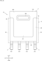
- FIG. 16 is a perspective view showing a semiconductor device according to a second embodiment of the present disclosure.
- FIG. 17 is a perspective view of essential parts showing a semiconductor device according to a second embodiment of the present disclosure.
- FIG. 18 is a plan view showing a semiconductor device according to a second embodiment of the present disclosure.
- FIG. 19 is a plan view of main parts showing a semiconductor device according to a second embodiment of the present disclosure.
- FIG. 19 is a plan view of main parts showing a semiconductor device according to a second embodiment of the present disclosure.
- FIG. 20 is a bottom view showing a semiconductor device according to a second embodiment of the present disclosure.
- FIG. 21 is a bottom view of essential parts showing a semiconductor device according to a second embodiment of the present disclosure.
- FIG. 22 is a cross-sectional view taken along line XXII-XXII in FIG. 21.
- FIG. 23 is a cross-sectional view taken along line XXIII-XXIII in FIG. 21.
- FIG. 24 is a cross-sectional view showing a first modification of the semiconductor device according to the second embodiment of the present disclosure.
- FIG. 25 is a cross-sectional view showing a second modification of the semiconductor device according to the second embodiment of the present disclosure.
- a thing A is formed on a thing B and "a thing A is formed on a thing B” mean “a thing A is formed on a thing B” unless otherwise specified.
- "something A is placed on something B” and “something A is placed on something B” mean "something A is placed on something B” unless otherwise specified.
- a certain surface A faces direction B means when the angle of the surface A with respect to the direction B is 90 degrees. This includes, but is not limited to, the case where the surface A is inclined with respect to the direction B.
- the semiconductor device A1 of this embodiment includes a semiconductor element 1, a first conductive member 2, a second conductive member 3, a third conductive member 4, a first bonding layer 7, a second bonding layer 8, and a sealing resin 9.
- the application of the semiconductor device A1 is not limited in any way, and is used, for example, in electronic equipment including a power conversion circuit, such as a DC-DC converter.
- FIG. 1 is a perspective view showing a semiconductor device A1.
- FIG. 2 is a perspective view of essential parts of the semiconductor device A1.
- FIG. 3 is a plan view showing the semiconductor device A1.
- FIG. 4 is a plan view of essential parts of the semiconductor device A1.
- FIG. 5 is a bottom view showing the semiconductor device A1.
- FIG. 6 is a bottom view of essential parts of the semiconductor device A1.
- FIG. 7 is a side view showing the semiconductor device A1.
- FIG. 8 is a cross-sectional view taken along line VIII-VIII in FIG. 4.
- FIG. 9 is a sectional view taken along line IX-IX in FIG. 4.
- FIG. 10 is a cross-sectional view of a main part schematically showing an example of a bonding structure included in the semiconductor device A1.
- the thickness direction of the present disclosure is defined as the thickness direction z.
- the first side in the thickness direction z is referred to as the z1 side, and the second side opposite to the first side in the z direction is referred to as the z2 side.
- one direction perpendicular to the thickness direction z is defined as a first direction x.
- the first side in the first direction x is referred to as the x1 side, and the second side opposite to the x1 side is referred to as the x2 side.
- a direction perpendicular to the thickness direction z and the first direction x is defined as a second direction y.
- the first side in the second direction y is referred to as the y1 side, and the second side opposite to the y1 side is referred to as the y2 side.
- the semiconductor element 1 is, for example, a MOSFET (Metal-Oxide-Semiconductor Field-Effect Transistor).
- the semiconductor element 1 may be a switching element such as an IGBT (Insulated Gate Bipolar Transistor) or a diode.
- IGBT Insulated Gate Bipolar Transistor
- the semiconductor element 1 is an n-channel type MOSFET with a vertical structure.
- the semiconductor element 1 has a semiconductor layer 10, a first electrode 11, a second electrode 12, and a third electrode 13, as shown in FIGS. 2, 4, and 8 to 10.
- FIG. 10 schematically shows a junction structure B1 included in a semiconductor device A1.
- the bonded structure B1 has a structure in which the semiconductor element 1, the first conductive member 2, the second conductive member 3, the first bonding layer 7, and the second bonding layer 8 are bonded to each other.
- the first conductive member 2 and the second conductive member 3 are shown protruding from the semiconductor element 1 in a plane including the first direction x and the second direction y.
- the fifth conductive member 6 and the first bonding layer 7 are shown to have a trapezoidal cross section that joins the semiconductor element 1 and the first conductive member 2 or the second conductive member 3.
- the semiconductor layer 10 is a layer containing a semiconductor.
- the composition of the semiconductor includes, for example, Si (silicon), SiC (silicon carbide), and the like. Further, unlike this embodiment, when the semiconductor element 1 is a switching element with a horizontal structure, the semiconductor layer 10 includes, for example, GaN (gallium nitride).
- the first electrode 11 is arranged on the z1 side of the semiconductor layer 10 in the thickness direction z. A current corresponding to the power converted by the semiconductor element 1 flows through the first electrode 11 . That is, the first electrode 11 corresponds to the source electrode of the semiconductor element 1.
- the second electrode 12 is arranged on the z2 side of the semiconductor layer 10 in the thickness direction z. A current corresponding to the power before being converted by the semiconductor element 1 flows through the second electrode 12 . That is, the second electrode 12 corresponds to the drain electrode of the semiconductor element 1.
- the third electrode 13 is arranged on the same z1 side as the first electrode 11 in the thickness direction z.
- a gate voltage for driving the semiconductor element 1 is applied to the third electrode 13 . That is, the third electrode 13 corresponds to the gate electrode of the semiconductor element 1.
- the area of the third electrode 13 is smaller than the area of the first electrode 11 when viewed in the thickness direction z.
- the first electrode 11 includes a first metal layer 111, a second metal layer 112, a first intermediate metal layer 113, and a first barrier metal layer 114.
- the first metal layer 111 includes a metal having higher thermal conductivity than solder.
- the first metal layer 111 contains a metal having higher thermal conductivity than solder as a main component.
- the first metal layer 111 contains, for example, Ag (silver) or Cu (copper). In the following description, the case where the first metal layer 111 has Ag (silver) as a main component will be described as an example.
- the first metal layer 111 mainly composed of Ag (silver) include an Ag (silver) sintered layer, an Ag (silver) paste layer, and an Ag (silver) formed by a film formation technique such as sputtering. layer, Ag (silver) plating layer, etc.
- the first metal layer 111 forms the surface layer of the first electrode 11 .
- the second metal layer 112 is interposed between the semiconductor layer 10 and the first metal layer 111.
- the second metal layer 112 is a layer containing Al (aluminum), for example.
- the thickness t111 of the first metal layer 111 and the thickness t112 of the second metal layer 112 are not limited at all.
- the thickness t111 is thicker than the thickness t112.
- the thickness t111 is, for example, 5 ⁇ m or more and 40 ⁇ m or less.
- the thickness t112 is, for example, 2 ⁇ m or more and 8 ⁇ m or less.
- the first intermediate metal layer 113 is interposed between the first metal layer 111 and the second metal layer 112.
- the first intermediate metal layer 113 contains, for example, Ti (titanium), Ni (nickel), or the like.
- the thickness of the first intermediate metal layer 113 is, for example, 0.1 ⁇ m or more and 0.6 ⁇ m or less.
- the first intermediate metal layer 113 is a layer for suppressing damage to the second metal layer 112 when forming the first metal layer 111 on the second metal layer 112, for example.
- the first barrier metal layer 114 is interposed between the second metal layer 112 and the semiconductor layer 10.
- the first barrier metal layer 114 includes, for example, TiN (titanium nitride).
- the thickness of the first barrier metal layer 114 is, for example, 0.01 ⁇ m or more and 0.1 ⁇ m or less.
- the first barrier metal layer 114 is a layer for suppressing damage to the semiconductor layer 10 when forming the second metal layer 112 on the semiconductor layer 10, for example.
- the second electrode 12 of this embodiment includes a fourth metal layer 122 and a second barrier metal layer 124.
- the fourth metal layer 122 is a layer containing Al (aluminum), for example.
- the fourth metal layer 122 forms the surface layer of the second electrode 12.
- the thickness of the fourth metal layer 122 is not limited at all, and may be the same as or different from the thickness t112 of the second metal layer 112.
- the second barrier metal layer 124 is interposed between the fourth metal layer 122 and the semiconductor layer 10.
- the second barrier metal layer 124 includes, for example, TiN (titanium nitride).
- the thickness of the second barrier metal layer 124 is, for example, 0.01 ⁇ m or more and 0.1 ⁇ m or less.
- the second barrier metal layer 124 is a layer for suppressing damage to the semiconductor layer 10 when forming the fourth metal layer 122 on the semiconductor layer 10, for example.
- the first conductive member 2 includes a portion disposed on the z1 side in the thickness direction z with respect to the semiconductor element 1.
- the first conductive member 2 includes a conductive material such as metal, and includes Cu (copper), for example.
- the first conductive member 2 has a first main surface 201 and a second main surface 202, as shown in FIGS. 1 to 10.
- the first main surface 201 is a surface facing the z1 side in the thickness direction z.
- the second main surface 202 is a surface facing the z2 side in the thickness direction z.
- the semiconductor element 1 is electrically connected to the second main surface 202 .
- the first main surface 201 is covered with the sealing resin 9 in this example.
- the first conductive member 2 has a first island portion 211, a plurality of first terminal portions 212, and a recessed portion 221, as shown in FIGS. 1 to 9.
- the first island portion 211 is a portion that is conductively bonded to the semiconductor element 1.
- the first island portion 211 includes a part of the first main surface 201 and a part of the second main surface 202.
- the shape and size of the first island portion 211 are not limited in any way, and in the illustrated example, it has a shape that overlaps all of the first electrode 11 when viewed in the thickness direction z, and also overlaps the third electrode 13. It has an exposed shape.
- the plurality of first terminal portions 212 are connected to the first island portion 211 on the y2 side in the second direction y.
- the plurality of first terminal parts 212 each extend in the second direction y when viewed in the thickness direction z, and are arranged at intervals in the first direction x.
- the number of the plurality of first terminal sections 212 is not limited at all, and may be three as in the illustrated example, two, or four or more. Alternatively, a configuration including only one first terminal portion 212 may be used.
- the first terminal portion 212 is connected to the first island portion 211 and covered with the sealing resin 9, and extends from the sealing resin 9 to the y2 side in the second direction y.
- the plurality of first terminal parts 212 are used as terminals when mounting the semiconductor device A1.
- the recessed portion 221 is a portion recessed from the first main surface 201 toward the z2 side in the thickness direction z.
- the recessed portion 221 overlaps the first island portion 211 when viewed in the thickness direction z.
- the first conductive member 2 includes a first base material 21 and a first plating layer 22.
- the first base material 21 is a main portion of the first conductive member 2, and includes, for example, Cu (copper).
- the first plating layer 22 is formed at a proper location on the first base material 21 and contains, for example, Ag (silver).
- the first plating layer 22 is provided at least at a location that is bonded to the semiconductor element 1 by the first bonding layer 7 .
- the first bonding layer 7 electrically connects the first electrode 11 of the semiconductor element 1 and the second main surface 202 of the first conductive member 2 .
- the first bonding layer 7 electrically connects the first metal layer 111 and the first plating layer 22.
- the specific structure of the first bonding layer 7 is not limited at all, and is made of, for example, a conductive bonding material such as solder or Ag (silver) plating.
- the thickness t7 of the first bonding layer 7 is not limited at all, and in this embodiment, it is thinner than the thickness t111 of the first metal layer 111.
- the thickness t7 is, for example, 4 ⁇ m or more and 30 ⁇ m or less.
- the second conductive member 3 is arranged on the z2 side in the thickness direction z with respect to the semiconductor element 1.
- the second conductive member 3 includes a conductive material such as metal, and includes Cu (copper), for example.
- the second conductive member 3 has a third main surface 301 and a fourth main surface 302, as shown in FIGS. 1 to 10.
- the third main surface 301 is a surface facing the z1 side in the thickness direction z.
- the fourth main surface 302 is a surface facing the z2 side in the thickness direction z.
- the semiconductor element 1 is mounted on the third main surface 301. As shown in FIGS. 5 and 6, the fourth main surface 302 is exposed from the sealing resin 9.
- the second conductive member 3 has a second island portion 311, a second terminal portion 312, a thin extension portion 321, and a through hole 322, as shown in FIGS. 1 to 9.
- the second island portion 311 is a portion on which all or a portion of the semiconductor element 1 is mounted.
- the second island portion 311 includes a part of the third main surface 301 and a part of the fourth main surface 302.
- the shape and size of the second island portion 311 are not limited in any way, and in the illustrated example, it has a substantially rectangular shape when viewed in the thickness direction z.
- the second terminal portion 312 is a portion connected to the second island portion 311 on the y1 side in the second direction y.
- the second terminal portion 312 includes a part of the third main surface 301 and a part of the fourth main surface 302.
- the second terminal portion 312 may be used as a terminal when mounting the semiconductor device A1.
- the thin extension portion 321 is a portion that includes the third main surface 301 and does not include the fourth main surface 302.
- the thickness of the thin extension portion 321 in the thickness direction z is thinner than the thickness of the second island portion 311 in the thickness direction z.
- the thin extension portion 321 extends from the second island portion 311 .
- the thin extension portion 321 extends from the second island portion 311 to the x1 side and the x2 side in the first direction x, and to the y2 side in the second direction y.
- the through hole 322 penetrates the second conductive member 3 in the thickness direction z.
- the through hole 322 is partially filled with the sealing resin 9.
- the size of the cross section of the through hole 322 perpendicular to the thickness direction z is larger on the z2 side than on the z1 side in the thickness direction z. This has the effect of suppressing, for example, the second conductive member 3 from falling off from the sealing resin 9.
- the second conductive member 3 includes a second base material 31 and a second plating layer 32.
- the second base material 31 is a main portion of the second conductive member 3, and includes, for example, Cu (copper).
- the second plating layer 32 is formed at a suitable location on the second base material 31 and contains, for example, Ag (silver).
- the second plating layer 32 is provided at least at a location where it is bonded to the semiconductor element 1 by the second bonding layer 8 .
- the second bonding layer 8 electrically connects the second electrode 12 of the semiconductor element 1 and the third main surface 301 of the second conductive member 3 .
- the second bonding layer 8 electrically connects the fourth metal layer 122 and the second plating layer 32.
- the specific structure of the second bonding layer 8 is not limited at all, and is made of, for example, a conductive bonding material such as solder or Ag (silver) plating. Note that, unlike this embodiment, when the semiconductor element 1 does not include the second electrode 12 on the z2 side in the thickness direction z, the second bonding layer 8 simply bonds the semiconductor element 1 and the second conductive member 3. However, a configuration may be adopted in which they are not electrically connected to each other.
- the third conductive member 4 includes a portion disposed on the z1 side in the thickness direction z with respect to the semiconductor element 1.
- the third conductive member 4 includes a conductive material such as metal, and includes Cu (copper), for example.
- the third conductive member 4 has a pad portion 411 and a third terminal portion 412, as shown in FIGS. 2 to 7.
- the pad portion 411 is a portion electrically connected to the third electrode 13 of the semiconductor element 1.
- the shape and size of the pad portion 411 are not limited in any way, and in the illustrated example, the pad portion 411 has a shape that overlaps a part of the third electrode 13 when viewed in the thickness direction z.
- the pad portion 411 is electrically connected to the third electrode 13 by solder or the like (not shown).
- the third terminal portion 412 is connected to the pad portion 411 on the y2 side in the second direction y.
- the third terminal portion 412 extends in the second direction y when viewed in the thickness direction z.
- the third terminal portion 412 is a portion connected to the pad portion 411 and covered with the sealing resin 9, and protrudes from the sealing resin 9 toward the y2 side in the second direction y. a portion folded back on the z2 side in the thickness direction z, and a portion located on the z2 side in the thickness direction z.
- the third terminal portion 412 has a shape and size that generally overlaps with the first terminal portion 212 when viewed in the first direction x.
- the third terminal portion 412 is used as a terminal when mounting the semiconductor device A1.
- the sealing resin 9 covers the semiconductor element 1 and a portion of each of the first conductive member 2, the second conductive member 3, and the third conductive member 4.
- the sealing resin 9 has electrical insulation properties.
- the sealing resin 9 includes, for example, a black epoxy resin containing filler.
- the shape of the sealing resin 9 is not limited at all. As shown in FIGS. 1 to 9, the sealing resin 9 of this embodiment has a first resin surface 91, a second resin surface 92, a third resin surface 93, a fourth resin surface 94, a fifth resin surface 95, and It has a sixth resin surface 96.
- the first resin surface 91 is a surface facing the z1 side in the thickness direction z.
- the second resin surface 92 is a surface facing the z2 side in the thickness direction z.
- the fourth main surface 302 of the second conductive member 3 is exposed from the second resin surface 92 .
- the first resin surface 91 and the second resin surface 92 are flat surfaces, but are not limited to this, and may be, for example, curved surfaces or bent surfaces.
- the second resin surface 92 and the fourth main surface 302 are flush with each other.
- the third resin surface 93 is a surface facing the x1 side in the first direction x.
- the fourth resin surface 94 is a surface facing the x2 side in the first direction x.
- the third resin surface 93 and the fourth resin surface 94 are slightly curved surfaces, but are not limited to this, and may be curved surfaces, flat surfaces, etc., for example.
- the fifth resin surface 95 is a surface facing the y1 side in the second direction y.
- the sixth resin surface 96 is a surface facing the y2 side in the second direction y.
- the fifth resin surface 95 and the sixth resin surface 96 are slightly curved surfaces, but are not limited to this, and may be curved surfaces, flat surfaces, etc., for example.
- a plurality of first terminal portions 212 and third terminal portions 412 protrude from the sixth resin surface 96 .
- the first electrode 11 includes a first metal layer 111.
- the first metal layer 111 includes a metal having higher thermal conductivity than solder.
- the semiconductor element 1 is a switching element with a vertical structure
- heat generation becomes significant in a portion of the semiconductor layer 10 located on the z1 side in the thickness direction z. It is reasonable to provide the first metal layer 111 as a measure to suppress the temperature rise due to such a tendency of heat generation.
- the heat flux of heat radiation from the semiconductor layer 10 can be further increased. It is preferable that the first metal layer 111 has Ag (silver) as a main component in order to increase heat flux.
- the configuration in which the first metal layer 111 is, for example, a sintered Ag (silver) layer is suitable for finishing the first metal layer 111 into a desired shape and thickness.
- the thickness t111 of the first metal layer 111 is thicker than the thickness t112 of the second metal layer 112. Thereby, heat from the semiconductor layer 10 can be more quickly transmitted to the first metal layer 111 via the second metal layer 112. Further, the thickness t7 of the first bonding layer 7 is thinner than the thickness t111 of the first metal layer 111. This allows the heat transferred to the first metal layer 111 to be transferred to the first conductive member 2 more efficiently, which is preferable for promoting heat dissipation from the semiconductor layer 10.
- FIG. 11 to 14 schematically show other examples of the bonding structure included in the semiconductor device A1.
- Various bonding structures including the bonding structure B1 described above and bonding structures B2 to B5 described below can be appropriately employed in various semiconductor devices including the semiconductor device A1 and the semiconductor device described below.
- the bonded structure B2 shown in FIG. 11 differs from the bonded structure B1 described above mainly in the configuration of the second electrode 12.
- the second electrode 12 of this example includes a third metal layer 121, a fourth metal layer 122, a second intermediate metal layer 123, and a second barrier metal layer 124.
- the third metal layer 121 includes a metal having higher thermal conductivity than solder.
- the third metal layer 121 contains a metal having higher thermal conductivity than solder as a main component.
- the third metal layer 121 contains, for example, Ag (silver) or Cu (copper). In the following description, a case where the third metal layer 121 has Ag (silver) as a main component will be described as an example.
- the third metal layer 121 containing Ag (silver) as a main component include, for example, an Ag (silver) sintered layer, an Ag (silver) paste layer, and an Ag (silver) formed by a film forming technique such as sputtering. layer, Ag (silver) plating layer, etc.
- the third metal layer 121 forms the surface layer of the second electrode 12 .
- the fourth metal layer 122 is interposed between the semiconductor layer 10 and the third metal layer 121.
- the fourth metal layer 122 is a layer containing Al (aluminum), for example.
- the thickness t121 of the third metal layer 121 and the thickness t122 of the fourth metal layer 122 are not limited at all. In this embodiment, the thickness t121 is thicker than the thickness t122.
- the thickness t121 is, for example, 5 ⁇ m or more and 10 ⁇ m or less.
- the thickness t122 is, for example, 2 ⁇ m or more and 8 ⁇ m or less.
- the second intermediate metal layer 123 is interposed between the third metal layer 121 and the fourth metal layer 122.
- the second intermediate metal layer 123 contains, for example, Ti (titanium), Ni (nickel), or the like.
- the thickness of the second intermediate metal layer 123 is, for example, 0.1 ⁇ m or more and 0.6 ⁇ m or less.
- the second intermediate metal layer 123 is a layer for suppressing damage to the fourth metal layer 122 when forming the third metal layer 121 on the fourth metal layer 122, for example.
- the second barrier metal layer 124 is interposed between the fourth metal layer 122 and the semiconductor layer 10.
- the second barrier metal layer 124 includes, for example, TiN (titanium nitride).
- the thickness of the second barrier metal layer 124 is, for example, 0.01 ⁇ m or more and 0.1 ⁇ m or less.
- the second barrier metal layer 124 is a layer for suppressing damage to the semiconductor layer 10 when forming the fourth metal layer 122 on the semiconductor layer 10, for example.
- the second bonding layer 8 has a similar configuration to the second bonding layer 8 of the bonding structure B1 described above.
- the thickness t8 of the second bonding layer 8 is not limited at all, and is thinner than the thickness t121 of the third metal layer 121 in this embodiment.
- the thickness t8 is, for example, 5 ⁇ m or more and 30 ⁇ m or less.
- the second electrode 12 includes the third metal layer 121.
- the third metal layer 121 includes a metal having higher thermal conductivity than solder.
- the heat flux of heat radiation from the semiconductor layer 10 can be further increased.
- the third metal layer 121 has Ag (silver) as its main component in order to increase the heat flux.
- the configuration in which the third metal layer 121 is, for example, a sintered Ag (silver) layer is suitable for finishing the third metal layer 121 into a desired shape and thickness.
- the thickness t121 of the third metal layer 121 is thicker than the thickness t122 of the fourth metal layer 122. Thereby, heat from the semiconductor layer 10 can be more quickly transmitted to the third metal layer 121 via the fourth metal layer 122. Further, the thickness t8 of the second bonding layer 8 is thinner than the thickness t121 of the third metal layer 121. This allows the heat transferred to the third metal layer 121 to be transferred to the second conductive member 3 more efficiently, which is preferable for promoting heat radiation from the semiconductor layer 10.
- the bonded structure B3 shown in FIG. 12 differs from the bonded structure B2 described above mainly in the configuration of the first electrode 11.
- the first electrode 11 of this example includes a first metal layer 111 and a first barrier metal layer 114, and the first metal layer 111 is formed on the first barrier metal layer 114.
- the thickness t111 is thicker than the thickness t7. In the case of the configuration of this example, the thickness t111 is, for example, 5 ⁇ m or more and 40 ⁇ m or less.
- the semiconductor element 1 it is possible to increase the heat flux of heat radiation from the semiconductor element 1, and the semiconductor element 1 can be operated more appropriately. Further, according to this example, it is possible to directly transfer heat from the semiconductor layer 10 to the first metal layer 111. This can be expected to further increase the heat flux of heat radiation. Further, by increasing the thickness t111, the heat capacity of the first metal layer 111 can be increased, and transient temperature rise of the semiconductor layer 10 can be suppressed more reliably.
- the bonded structure B4 shown in FIG. 13 differs from the bonded structure B3 described above mainly in the configuration of the second electrode 12.
- the second electrode 12 of this example includes a third metal layer 121 and a second barrier metal layer 124 , and the third metal layer 121 is formed on the second barrier metal layer 124 .
- the thickness t121 is thicker than the thickness t8. In the case of the configuration of this example, the thickness t121 is, for example, 5 ⁇ m or more and 40 ⁇ m or less.
- the semiconductor element 1 it is possible to increase the heat flux of heat radiation from the semiconductor element 1, and the semiconductor element 1 can be operated more appropriately. Further, according to this example, it is possible to directly transfer heat from the semiconductor layer 10 to the third metal layer 121. This can be expected to further increase the heat flux of heat radiation. Further, by increasing the thickness t121, the heat capacity of the third metal layer 121 can be increased, and transient temperature rise of the semiconductor layer 10 can be suppressed more reliably.
- the bonded structure B5 shown in FIG. 14 differs from the bonded structures B1 to B4 described above mainly in that it does not include the first bonding layer 7 and the second bonding layer 8.
- the first metal layer 111 of the first electrode 11 is directly joined to the first plating layer 22 of the first conductive member 2.
- the first metal layer 111 and the first plating layer 22 have the same metal such as Ag (silver) as a main component, such a structure is such that they are joined by solid phase diffusion bonding. Illustrated.
- the first metal layer 111 is made of a sintered Ag (silver) layer
- a sintered paste for forming the first metal layer 111 is placed on the first intermediate metal layer 113, and further the sintered paste is By placing the first conductive member 2 on top and then sintering the sintered paste, the first metal layer 111 is formed and the first electrode 11 and the first conductive member 2 are bonded. May be achieved.
- the third metal layer 121 of the second electrode 12 is directly joined to the second plating layer 32 of the second conductive member 3.
- a structure in which they are joined by solid phase diffusion bonding. Illustrated.
- the third metal layer 121 is made of a sintered Ag (silver) layer
- a sintered paste for forming the third metal layer 121 is placed on the second conductive member 3, and the sintered paste is further
- the second intermediate metal layer 123 is placed on the sintered paste and then sintering the sintered paste, the third metal layer 121 is formed and the second electrode 12 and the second conductive member 3 are bonded to each other. May be achieved.
- heat can be directly transmitted from the first metal layer 111 to the first conductive member 2 without going through the first bonding layer 7 . This makes it possible to further suppress transient temperature rise in the semiconductor layer 10 and promote steady heat dissipation over a longer period of time.
- heat can be directly transmitted from the third metal layer 121 to the second conductive member 3 without going through the second bonding layer 8 . This makes it possible to further suppress transient temperature rise in the semiconductor layer 10 and promote steady heat dissipation over a longer period of time.
- FIG. 15 shows a first modification of the semiconductor device A1.
- the semiconductor device A11 of this modification differs from the above-described semiconductor device A1 mainly in the configuration of the first conductive member 2 and the sealing resin 9.
- the first main surface 201 is exposed from the first resin surface 91 of the sealing resin 9.
- the first conductive member 2 does not have the above-mentioned recess 221 formed therein. Further, the first main surface 201 and the first resin surface 91 are flush with each other.
- the semiconductor device A2 of this embodiment includes a semiconductor element 1, a first conductive member 2, a second conductive member 3, a third conductive member 4, a fourth conductive member 5, a fifth conductive member 6, and a sealing resin 9.
- the first conductive member 2 has a first island portion 211 and a connecting portion 213.
- the first island portion 211 includes a portion of each of the first main surface 201 and the second main surface 202, and is electrically connected to the first electrode 11 of the semiconductor element 1.
- the connecting portion 213 is a portion located on the y2 side in the second direction y with respect to the first island portion 211.
- the connecting portion 213 has a portion extending from the first island portion 211 toward the y2 side in the second direction y, and a portion further extending toward the z2 side in the thickness direction z.
- the first main surface 201 of the first conductive member 2 is exposed from the first resin surface 91 of the sealing resin 9.
- the first main surface 201 and the first resin surface 91 are flush with each other.
- the fourth conductive member 5 is arranged on the z2 side in the thickness direction z with respect to the first conductive member 2.
- the fourth conductive member 5 includes a conductive material such as metal, and includes Cu (copper), for example. Furthermore, a plating layer (not shown) may be provided at an appropriate location on the fourth conductive member 5.
- the fourth conductive member 5 is conductively bonded to the connecting portion 213 of the semiconductor element 1 by a conductive bonding material 59 such as solder.
- the fourth conductive member 5 has a seventh main surface 501 and an eighth main surface 502, as shown in FIGS. 16, 17, and 19 to 22.
- the seventh main surface 501 is a surface facing the z1 side in the thickness direction z.
- the eighth main surface 502 is a surface facing the z2 side in the thickness direction z.
- the connecting portion 213 of the first conductive member 2 is electrically connected to the seventh main surface 501 by a conductive bonding material 59 .
- the seventh main surface 501 is covered with a sealing resin 9.
- the eighth main surface 502 is exposed from the second resin surface 92 of the sealing resin 9. In this example, the eighth main surface 502 and the second resin surface 92 are flush with each other.
- the fourth conductive member 5 has a pad portion 511, a plurality of fourth terminal portions 512, and a thin extension portion 521.
- the pad portion 511 is a portion electrically connected to the first conductive member 2.
- the pad portion 511 includes a part of the seventh main surface 501 and a part of the eighth main surface 502.
- the shape and size of the pad portion 511 are not limited at all, and in the illustrated example, it is a long rectangular shape whose longitudinal direction is the first direction x when viewed from the thickness direction z.
- the plurality of fourth terminal portions 512 are connected to the pad portion 511 on the y2 side in the second direction y.
- the plurality of fourth terminal parts 512 each extend in the second direction y when viewed in the thickness direction z, and are arranged at intervals in the first direction x.
- the number of the plurality of fourth terminal parts 512 is not limited at all, and may be three as in the illustrated example, two, or four or more. Alternatively, a configuration including only one fourth terminal portion 512 may be used.
- the fourth terminal portion 512 is exposed from the second resin surface 92 and the sixth resin surface 96 of the sealing resin 9. As shown in FIG. The distal end surface of the fourth terminal portion 512 is flush with the sixth resin surface 96.
- the plurality of fourth terminal parts 512 are used as terminals when mounting the semiconductor device A2.
- the thin extension portion 521 is a portion that includes the seventh main surface 501 and does not include the eighth main surface 502.
- the thickness of the thin extension portion 521 in the thickness direction z is thinner than the thickness of the pad portion 511 in the thickness direction z.
- the thin extension portion 521 extends from the pad portion 511. In the illustrated example, the thin extension portion 521 extends from the pad portion 511 to the x1 side and the x2 side in the first direction x, and to the y1 side in the second direction y.
- the second conductive member 3 of this embodiment includes a second island portion 311, a plurality of second terminal portions 312, a thin extension portion 321, and a thick extension portion 321. 323.
- the second island portion 311 is a portion on which all or a portion of the semiconductor element 1 is mounted, and has a similar configuration to the second island portion 311 of the semiconductor device A1.
- the plurality of second terminal parts 312 are parts connected to the second island part 311 on the y1 side in the second direction y.
- the second terminal portion 312 includes a part of the third main surface 301 and a part of the fourth main surface 302.
- the second terminal portion 312 may be used as a terminal when mounting the semiconductor device A1.
- the plurality of second terminal portions 312 are connected to the second island portion 311 on the y1 side in the second direction y.
- the plurality of second terminal portions 312 each extend in the second direction y when viewed in the thickness direction z, and are arranged at intervals in the first direction x.
- the number of the plurality of second terminal parts 312 is not limited at all, and may be four as in the illustrated example, or may be two, three, or five or more. Alternatively, a configuration including only one second terminal portion 312 may be used.
- the second terminal portion 312 is exposed from the second resin surface 92 and the fifth resin surface 95 of the sealing resin 9. As shown in FIG. The tip end surface of the second terminal portion 312 is flush with the fifth resin surface 95.
- the plurality of second terminal sections 312 are used as terminals when mounting the semiconductor device A2.
- the thick extension portion 323 protrudes from the second island portion 311 in the first direction x.
- the thick extension portion 323 includes a part of the third main surface 301 and a part of the fourth main surface 302.
- the second conductive member 3 has two thick extensions 323 .
- the two thick extensions 323 protrude from the second island portion 311 on both sides in the first direction x.
- the two thick extensions 323 are exposed from the second resin surface 92 , third resin surface 93 , and fourth resin surface 94 of the sealing resin 9 .
- the tip surfaces of the two thick extensions 323 are flush with the third resin surface 93 and the fourth resin surface 94.
- the third conductive member 4 is disposed on the y2 side in the second direction y with respect to the second conductive member 3, and is disposed on the x1 side in the first direction x with respect to the fourth conductive member 5.
- the third conductive member 4 includes a conductive material such as metal, and includes Cu (copper), for example. Furthermore, a plating layer (not shown) may be provided at an appropriate location on the third conductive member 4.
- a fifth conductive member 6 is connected to the third conductive member 4 .
- the third conductive member 4 has a fifth main surface 401 and a sixth main surface 402, as shown in FIGS. 16, 17, and 19 to 21.
- the fifth main surface 401 is a surface facing the z1 side in the thickness direction z.
- the sixth main surface 402 is a surface facing the z2 side in the thickness direction z.
- the fifth conductive member 6 is connected to the fifth main surface 401 .
- the fifth main surface 401 is covered with a sealing resin 9.
- the sixth main surface 402 is exposed from the second resin surface 92 of the sealing resin 9. In this example, the sixth main surface 402 and the second resin surface 92 are flush with each other.
- the third conductive member 4 has a pad portion 411, a third terminal portion 412, and a thin extension portion 421.
- the pad portion 411 is a portion to which the fifth conductive member 6 is connected.
- the pad portion 411 includes a part of the fifth main surface 401 and a part of the sixth main surface 402.
- the shape and size of the pad portion 411 are not limited at all, and in the illustrated example, it has a rectangular shape when viewed in the thickness direction z. Further, the size of the pad portion 411 in the first direction x is smaller than the size of the pad portion 511 in the first direction x.
- the third terminal portion 412 is connected to the pad portion 411 on the y2 side in the second direction y.
- the third terminal portion 412 extends in the second direction y when viewed in the thickness direction z.
- the number of third terminal portions 412 is not limited at all, and may be one as in the illustrated example, or two or more.
- the third terminal portion 412 is exposed from the second resin surface 92 and the sixth resin surface 96 of the sealing resin 9.
- the distal end surface of the third terminal portion 412 is flush with the sixth resin surface 96.
- the plurality of third terminal sections 412 are used as terminals when mounting the semiconductor device A2.
- the thin extension portion 421 is a portion that includes the fifth main surface 401 but does not include the sixth main surface 402.
- the thickness of the thin extension portion 421 in the thickness direction z is thinner than the thickness of the pad portion 411 in the thickness direction z.
- the thin extension portion 421 extends from the pad portion 411. In the illustrated example, the thin extension portion 421 extends from the pad portion 411 to the x1 side and the x2 side in the first direction x, and to the y1 side in the second direction y.
- the fifth conductive member 6 is connected to the third electrode 13 of the semiconductor element 1 and the pad portion 411 of the third conductive member 4.
- the fifth conductive member 6 is a wire whose main component is a metal such as Au (gold), Cu (copper), or Al (aluminum).
- the fifth conductive member 6 may be made of a wide ribbon-shaped metal member or a lead member instead of the wire.
- the semiconductor element 1 can be operated more appropriately.
- the thickness of the first conductive member 2 in the thickness direction z can be changed from the thickness of the fourth conductive member 5 in the thickness direction z. It is possible to more easily achieve configurations with a thickness greater than .
- FIG. 24 shows a first modification of the semiconductor device A2.
- the semiconductor device A21 of this modification differs from the above-described semiconductor device A2 mainly in the configuration of the first conductive member 2.
- the first island portion 211 of the first conductive member 2 protrudes from the first resin surface 91 of the sealing resin 9 toward the z1 side in the thickness direction z.
- the first main surface 201 is located closer to the z1 side than the first resin surface 91 in the thickness direction z.
- the semiconductor element 1 can be operated more appropriately. Furthermore, when attaching the semiconductor device A21 to a heat sink (not shown) or the like, since the first main surface 201 is located on the z1 side in the thickness direction z from the first resin surface 91, the first main surface 201 can be attached to a heat sink (not shown) or the like. It has the advantage of being easy to press against the heat sink. Thereby, heat dissipation from the semiconductor device A21 can be further promoted.
- FIG. 25 shows a second modification of the semiconductor device A2.
- the semiconductor device A22 of this modification differs from the above-described example mainly in the configuration of the first conductive member 2.
- the first conductive member 2 has a plurality of protrusions 223.
- the plurality of convex portions 223 protrude from the first main surface 201 toward the z1 side in the thickness direction z.
- the shape and arrangement of the plurality of protrusions 223 when viewed in the thickness direction z are not limited at all.
- the plurality of convex portions 223 may be arranged, for example, in a matrix when viewed in the thickness direction z.
- the convex portion 223 may have a fin shape extending along the first direction x or the second direction y.
- the positional relationship between the first main surface 201 and the first resin surface 91 in this example is not limited at all.
- the first main surface 201 may be located on the z1 side in the thickness direction z than the first resin surface 91. There is.
- the semiconductor element 1 it is possible to increase the heat flux of heat radiation from the semiconductor element 1, and the semiconductor element 1 can be operated more appropriately. Further, since the first conductive member 2 has a plurality of convex portions 223, it is possible to increase the area from which heat is radiated from the first conductive member 2. Thereby, heat dissipation from the semiconductor device A22 can be further promoted.
- the semiconductor device according to the present disclosure is not limited to the embodiments described above.
- the specific configuration of each part of the semiconductor device according to the present disclosure can be changed in design in various ways.
- a semiconductor element having a semiconductor layer and a first electrode disposed on a first side of the semiconductor layer in the thickness direction; a first conductive member joined to the first electrode; a second conductive member joined to the semiconductor element from the second side in the thickness direction; a first resin surface facing the first side in the thickness direction and a second resin surface facing the second side, the semiconductor element and at least one of each of the first conductive member and the second conductive member; and a sealing resin covering the portion,
- the first electrode includes a first metal layer containing a metal having higher thermal conductivity than solder. Appendix 2.
- Appendix 9. The semiconductor device according to any one of appendices 1 to 8, further comprising a first bonding layer that bonds the first electrode and the first conductive member.
- Appendix 10. The semiconductor device according to appendix 9, wherein the first metal layer has a thickness greater than the first bonding layer.
- Appendix 11. 9. The semiconductor device according to any one of appendices 1 to 8, wherein the first metal layer is in direct contact with the first conductive member.
- Appendix 12. The semiconductor element has a second electrode disposed on the second side of the semiconductor layer in the thickness direction, 12.
- the semiconductor device according to any one of appendices 1 to 11, wherein the second electrode includes a third metal layer containing a metal having higher thermal conductivity than solder. Appendix 13. The semiconductor device according to appendix 12, wherein the third metal layer contains Ag or Cu. Appendix 14. further comprising a second bonding layer bonding the second electrode and the second conductive member, The semiconductor device according to appendix 12 or 13, wherein the third metal layer is thicker than the second bonding layer. Appendix 15. further comprising a third conductive member electrically connected to the third electrode, 15. The semiconductor device according to any one of appendices 1 to 14, wherein the semiconductor element has a third electrode disposed on the first side of the semiconductor layer in the thickness direction. Appendix 16. 16.
- the semiconductor device according to any one of appendices 1 to 15, wherein the first conductive member has a first terminal portion including a portion located on the second side in the thickness direction with respect to the semiconductor element.
- Appendix 17. further comprising a fourth conductive member electrically connected to the first conductive member, The semiconductor device according to appendix 15, wherein the fourth conductive member has a portion located on the second side in the thickness direction with respect to the semiconductor element.
- A1, A11, A2, A21, A22 Semiconductor devices B1, B2, B3, B4, B5: Junction structure 1: Semiconductor element 2: First conductive member 3: Second conductive member 4: Third conductive member 5: Third conductive member 4 conductive member 6: fifth conductive member 7: first bonding layer 8: second bonding layer 9: sealing resin 10: semiconductor layer 11: first electrode 12: second electrode 13: third electrode 21: first group Material 22: First plating layer 31: Second base material 32: Second plating layer 59: Conductive bonding material 91: First resin surface 92: Second resin surface 93: Third resin surface 94: Fourth resin surface 95 : Fifth resin surface 96: Sixth resin surface 111: First metal layer 112: Second metal layer 113: First intermediate metal layer 114: First barrier metal layer 121: Third metal layer 122: Fourth metal layer 123 : Second intermediate metal layer 124: Second barrier metal layer 201: First main surface 202: Second main surface 211: First island portion 212: First terminal portion 213: Connection portion 221
Landscapes
- Cooling Or The Like Of Semiconductors Or Solid State Devices (AREA)
- Structures Or Materials For Encapsulating Or Coating Semiconductor Devices Or Solid State Devices (AREA)
Priority Applications (4)
| Application Number | Priority Date | Filing Date | Title |
|---|---|---|---|
| JP2024538942A JPWO2024029385A1 (https=) | 2022-08-05 | 2023-07-24 | |
| CN202380055933.8A CN119631175A (zh) | 2022-08-05 | 2023-07-24 | 半导体装置 |
| DE112023003350.1T DE112023003350T5 (de) | 2022-08-05 | 2023-07-24 | Halbleitervorrichtung |
| US19/040,553 US20250174527A1 (en) | 2022-08-05 | 2025-01-29 | Semiconductor device |
Applications Claiming Priority (2)
| Application Number | Priority Date | Filing Date | Title |
|---|---|---|---|
| JP2022125359 | 2022-08-05 | ||
| JP2022-125359 | 2022-08-05 |
Related Child Applications (1)
| Application Number | Title | Priority Date | Filing Date |
|---|---|---|---|
| US19/040,553 Continuation US20250174527A1 (en) | 2022-08-05 | 2025-01-29 | Semiconductor device |
Publications (1)
| Publication Number | Publication Date |
|---|---|
| WO2024029385A1 true WO2024029385A1 (ja) | 2024-02-08 |
Family
ID=89848936
Family Applications (1)
| Application Number | Title | Priority Date | Filing Date |
|---|---|---|---|
| PCT/JP2023/027007 Ceased WO2024029385A1 (ja) | 2022-08-05 | 2023-07-24 | 半導体装置 |
Country Status (5)
| Country | Link |
|---|---|
| US (1) | US20250174527A1 (https=) |
| JP (1) | JPWO2024029385A1 (https=) |
| CN (1) | CN119631175A (https=) |
| DE (1) | DE112023003350T5 (https=) |
| WO (1) | WO2024029385A1 (https=) |
Citations (6)
| Publication number | Priority date | Publication date | Assignee | Title |
|---|---|---|---|---|
| JP2006066813A (ja) * | 2004-08-30 | 2006-03-09 | Renesas Technology Corp | 半導体装置 |
| JP2015142072A (ja) * | 2014-01-30 | 2015-08-03 | 株式会社東芝 | 半導体装置 |
| JP2017050489A (ja) * | 2015-09-04 | 2017-03-09 | 株式会社東芝 | 半導体パッケージおよび半導体パッケージの製造方法 |
| JP2019169610A (ja) * | 2018-03-23 | 2019-10-03 | 株式会社東芝 | 半導体装置 |
| JP2021027116A (ja) * | 2019-08-02 | 2021-02-22 | ローム株式会社 | 半導体装置 |
| JP2021158180A (ja) * | 2020-03-26 | 2021-10-07 | ローム株式会社 | 半導体装置 |
-
2023
- 2023-07-24 CN CN202380055933.8A patent/CN119631175A/zh active Pending
- 2023-07-24 DE DE112023003350.1T patent/DE112023003350T5/de active Pending
- 2023-07-24 JP JP2024538942A patent/JPWO2024029385A1/ja active Pending
- 2023-07-24 WO PCT/JP2023/027007 patent/WO2024029385A1/ja not_active Ceased
-
2025
- 2025-01-29 US US19/040,553 patent/US20250174527A1/en active Pending
Patent Citations (6)
| Publication number | Priority date | Publication date | Assignee | Title |
|---|---|---|---|---|
| JP2006066813A (ja) * | 2004-08-30 | 2006-03-09 | Renesas Technology Corp | 半導体装置 |
| JP2015142072A (ja) * | 2014-01-30 | 2015-08-03 | 株式会社東芝 | 半導体装置 |
| JP2017050489A (ja) * | 2015-09-04 | 2017-03-09 | 株式会社東芝 | 半導体パッケージおよび半導体パッケージの製造方法 |
| JP2019169610A (ja) * | 2018-03-23 | 2019-10-03 | 株式会社東芝 | 半導体装置 |
| JP2021027116A (ja) * | 2019-08-02 | 2021-02-22 | ローム株式会社 | 半導体装置 |
| JP2021158180A (ja) * | 2020-03-26 | 2021-10-07 | ローム株式会社 | 半導体装置 |
Also Published As
| Publication number | Publication date |
|---|---|
| DE112023003350T5 (de) | 2025-05-15 |
| JPWO2024029385A1 (https=) | 2024-02-08 |
| CN119631175A (zh) | 2025-03-14 |
| US20250174527A1 (en) | 2025-05-29 |
Similar Documents
| Publication | Publication Date | Title |
|---|---|---|
| JP7419781B2 (ja) | 半導体モジュール | |
| US11133271B2 (en) | Semiconductor device | |
| JP5678884B2 (ja) | 電力変換装置 | |
| JP7795476B2 (ja) | 半導体装置 | |
| JP2025142343A (ja) | 半導体装置 | |
| WO2024116873A1 (ja) | 半導体モジュール | |
| WO2023100659A1 (ja) | 半導体装置 | |
| JP7545845B2 (ja) | 半導体装置 | |
| JPWO2020149225A1 (ja) | 半導体装置 | |
| WO2024029385A1 (ja) | 半導体装置 | |
| WO2023149257A1 (ja) | 半導体装置 | |
| WO2024018790A1 (ja) | 半導体装置 | |
| WO2023100663A1 (ja) | 半導体装置 | |
| WO2022145266A1 (ja) | 半導体装置、および半導体装置の製造方法 | |
| US20220084900A1 (en) | Semiconductor device | |
| JP7661796B2 (ja) | 半導体装置 | |
| JP2026035927A (ja) | 半導体装置 | |
| US20240047315A1 (en) | Semiconductor device | |
| JP7704594B2 (ja) | 半導体装置 | |
| JP2024013111A (ja) | 半導体素子および半導体装置 | |
| WO2025142395A1 (ja) | 半導体装置 | |
| JP2023163856A (ja) | 半導体装置 | |
| WO2024106219A1 (ja) | 半導体装置 | |
| WO2024075589A1 (ja) | 半導体装置 | |
| WO2024219218A1 (ja) | 半導体装置および車両 |
Legal Events
| Date | Code | Title | Description |
|---|---|---|---|
| 121 | Ep: the epo has been informed by wipo that ep was designated in this application |
Ref document number: 23849940 Country of ref document: EP Kind code of ref document: A1 |
|
| WWE | Wipo information: entry into national phase |
Ref document number: 2024538942 Country of ref document: JP |
|
| WWE | Wipo information: entry into national phase |
Ref document number: 202380055933.8 Country of ref document: CN |
|
| WWE | Wipo information: entry into national phase |
Ref document number: 112023003350 Country of ref document: DE |
|
| WWP | Wipo information: published in national office |
Ref document number: 202380055933.8 Country of ref document: CN |
|
| WWP | Wipo information: published in national office |
Ref document number: 112023003350 Country of ref document: DE |
|
| 122 | Ep: pct application non-entry in european phase |
Ref document number: 23849940 Country of ref document: EP Kind code of ref document: A1 |