WO2024004985A1 - 電子部品 - Google Patents
電子部品 Download PDFInfo
- Publication number
- WO2024004985A1 WO2024004985A1 PCT/JP2023/023730 JP2023023730W WO2024004985A1 WO 2024004985 A1 WO2024004985 A1 WO 2024004985A1 JP 2023023730 W JP2023023730 W JP 2023023730W WO 2024004985 A1 WO2024004985 A1 WO 2024004985A1
- Authority
- WO
- WIPO (PCT)
- Prior art keywords
- conductor
- substrate
- planar
- electronic component
- conductors
- Prior art date
- Legal status (The legal status is an assumption and is not a legal conclusion. Google has not performed a legal analysis and makes no representation as to the accuracy of the status listed.)
- Ceased
Links
Images


Classifications
-
- H—ELECTRICITY
- H10—SEMICONDUCTOR DEVICES; ELECTRIC SOLID-STATE DEVICES NOT OTHERWISE PROVIDED FOR
- H10W—GENERIC PACKAGES, INTERCONNECTIONS, CONNECTORS OR OTHER CONSTRUCTIONAL DETAILS OF DEVICES COVERED BY CLASS H10
- H10W20/00—Interconnections in chips, wafers or substrates
- H10W20/40—Interconnections external to wafers or substrates, e.g. back-end-of-line [BEOL] metallisations or vias connecting to gate electrodes
- H10W20/497—Inductive arrangements or effects of, or between, wiring layers
-
- H—ELECTRICITY
- H01—ELECTRIC ELEMENTS
- H01F—MAGNETS; INDUCTANCES; TRANSFORMERS; SELECTION OF MATERIALS FOR THEIR MAGNETIC PROPERTIES
- H01F17/00—Fixed inductances of the signal type
-
- H—ELECTRICITY
- H01—ELECTRIC ELEMENTS
- H01F—MAGNETS; INDUCTANCES; TRANSFORMERS; SELECTION OF MATERIALS FOR THEIR MAGNETIC PROPERTIES
- H01F27/00—Details of transformers or inductances, in general
-
- H—ELECTRICITY
- H10—SEMICONDUCTOR DEVICES; ELECTRIC SOLID-STATE DEVICES NOT OTHERWISE PROVIDED FOR
- H10D—INORGANIC ELECTRIC SEMICONDUCTOR DEVICES
- H10D84/00—Integrated devices formed in or on semiconductor substrates that comprise only semiconducting layers, e.g. on Si wafers or on GaAs-on-Si wafers
-
- H—ELECTRICITY
- H10—SEMICONDUCTOR DEVICES; ELECTRIC SOLID-STATE DEVICES NOT OTHERWISE PROVIDED FOR
- H10W—GENERIC PACKAGES, INTERCONNECTIONS, CONNECTORS OR OTHER CONSTRUCTIONAL DETAILS OF DEVICES COVERED BY CLASS H10
- H10W20/00—Interconnections in chips, wafers or substrates
- H10W20/01—Manufacture or treatment
-
- H—ELECTRICITY
- H10—SEMICONDUCTOR DEVICES; ELECTRIC SOLID-STATE DEVICES NOT OTHERWISE PROVIDED FOR
- H10W—GENERIC PACKAGES, INTERCONNECTIONS, CONNECTORS OR OTHER CONSTRUCTIONAL DETAILS OF DEVICES COVERED BY CLASS H10
- H10W20/00—Interconnections in chips, wafers or substrates
- H10W20/40—Interconnections external to wafers or substrates, e.g. back-end-of-line [BEOL] metallisations or vias connecting to gate electrodes
- H10W20/495—Capacitive arrangements or effects of, or between wiring layers
- H10W20/496—Capacitor integral with wiring layers
-
- H—ELECTRICITY
- H10—SEMICONDUCTOR DEVICES; ELECTRIC SOLID-STATE DEVICES NOT OTHERWISE PROVIDED FOR
- H10W—GENERIC PACKAGES, INTERCONNECTIONS, CONNECTORS OR OTHER CONSTRUCTIONAL DETAILS OF DEVICES COVERED BY CLASS H10
- H10W20/00—Interconnections in chips, wafers or substrates
- H10W20/40—Interconnections external to wafers or substrates, e.g. back-end-of-line [BEOL] metallisations or vias connecting to gate electrodes
- H10W20/498—Resistive arrangements or effects of, or between, wiring layers
-
- H—ELECTRICITY
- H10—SEMICONDUCTOR DEVICES; ELECTRIC SOLID-STATE DEVICES NOT OTHERWISE PROVIDED FOR
- H10D—INORGANIC ELECTRIC SEMICONDUCTOR DEVICES
- H10D1/00—Resistors, capacitors or inductors
- H10D1/20—Inductors
-
- H—ELECTRICITY
- H10—SEMICONDUCTOR DEVICES; ELECTRIC SOLID-STATE DEVICES NOT OTHERWISE PROVIDED FOR
- H10D—INORGANIC ELECTRIC SEMICONDUCTOR DEVICES
- H10D1/00—Resistors, capacitors or inductors
- H10D1/60—Capacitors
- H10D1/62—Capacitors having potential barriers
-
- H—ELECTRICITY
- H10—SEMICONDUCTOR DEVICES; ELECTRIC SOLID-STATE DEVICES NOT OTHERWISE PROVIDED FOR
- H10D—INORGANIC ELECTRIC SEMICONDUCTOR DEVICES
- H10D1/00—Resistors, capacitors or inductors
- H10D1/60—Capacitors
- H10D1/68—Capacitors having no potential barriers
- H10D1/692—Electrodes
Definitions
- the present invention relates to an electronic component including a helical coil inductor and a planar conductor.
- a coil component in which a helical coil is formed on a substrate is used as an inductor.
- Patent Document 1 shows a coil component.
- the coil component of Patent Document 1 is produced by cutting into chips a core substrate on which a plurality of band-shaped conductors and an insulating layer covering the band-shaped conductors are formed on the front and back surfaces.
- this coil component has a plurality of side conductors made of band-shaped conductors and an insulating layer covering the side conductors on both left and right side surfaces of a rectangular parallelepiped insulator made of a core substrate.
- a rectangular helical coil is formed by having a side conductor and a bridge conductor that connects these on the upper and lower surfaces of the insulator.
- Patent Document 2 shows a wiring board.
- the wiring board of Patent Document 2 includes a first insulating layer formed without a core material, and a first conductor layer and a second conductor layer that are provided to face each other with the first insulating layer interposed therebetween. , a plurality of via conductors that penetrate the first insulating layer and connect the first conductor layer and the second conductor layer.
- the first conductor layer and the second conductor layer are adjacent to each other with the first insulating layer interposed therebetween.
- the magnetic material having a predetermined shape is buried in the first insulating layer so as not to contact any of the first conductor layer, the second conductor layer, and the plurality of via conductors.
- a coil is formed around the magnetic material by wiring patterns included in each of the first conductor layer and the second conductor layer, and a plurality of via conductors. The coil extends along a direction intersecting the stacking direction of the wiring board.
- an inductor When constructing an inductor on a conductive substrate such as a doped silicon substrate, it is effective to arrange the opening direction of the magnetic flux of the helical coil parallel to the substrate so that its Q value does not deteriorate. That is, the magnetic flux generated by the coil does not penetrate the substrate, and losses due to eddy currents can be reduced.
- this inductor is made into a component and placed on a circuit board together with elements such as conductors and other electronic components, when combining the above-mentioned inductor with a capacitor to form an LC composite component such as an LC filter or an impedance matching circuit, The following issues arise.
- the helical coil When making a helical coil like the coil parts described in Patent Document 1 and Patent Document 2, the helical coil is formed along a plane parallel to the surface of the substrate. However, if other electronic components are formed close to the opening of the helical coil, eddy currents due to the magnetic field of the helical coil will occur in the conductor of this electronic component, deteriorating the electrical characteristics of the composite component. Resulting in.
- either the top surface or the bottom surface of the plane parallel to the surface of the substrate is the starting end or the terminal end.
- an internal wiring conductive to a terminal or other element is formed near the opening of the helical coil, eddy currents due to the magnetic field will occur in the internal wiring, degrading the electrical characteristics of the composite component.
- an object of the present invention is to provide an electronic component having a helical coil in which the aperture direction of the magnetic flux of the helical coil is arranged parallel to a substrate, even when the helical coil is mounted together with other conductors, electronic components, etc.
- An object of the present invention is to provide an electronic component that allows miniaturization of an electronic device in which the electronic component and other elements are mounted.
- Another object of the present invention is to provide a small-sized electronic component that includes an inductor having a predetermined inductance and internal wiring.
- An electronic component as an example of the present disclosure includes: a substrate, an insulator layer formed along a surface of the substrate, an inductor formed in the insulator layer, and one or more inductors formed in the substrate or the insulator layer and extending along the substrate. a planar conductor, and one or more planar conductor connection conductors electrically connected to the planar conductor,
- the inductor includes a plurality of planar conductors each extending in a plurality of layers along the surface of the substrate, and a plurality of inductor via conductors that connect the planar conductors extending in different layers among the plurality of layers.
- an inductor using a helical coil having a winding axis along the surface of the substrate The direction of the current flowing through the inductor via conductor adjacent to the planar conductor connecting conductor among the plurality of inductor via conductors and the direction of the current flowing through the planar conductor connecting conductor are opposite to each other. It is characterized by
- an electronic component having a helical coil in which the opening direction of the magnetic flux of the helical coil is arranged parallel to a substrate when the electronic component having the helical coil is mounted together with other conductors, electronic components, etc.
- An electronic component can be obtained that allows miniaturization of an electronic device in which the component and other elements are mounted, and a small-sized electronic component that includes an inductor having a predetermined inductance and internal wiring can be obtained.
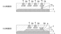
- FIG. 1 is a diagram showing the structure of an electronic component 101 according to the first embodiment.
- FIG. 2 is an equivalent circuit diagram of the electronic component 101.
- FIG. 3(A) is a plan view showing the positional relationship between the electronic component 101 and another member 201 adjacent thereto.
- FIG. 3B is a plan view showing the positional relationship between an electronic component 301 as a comparative example and a member 201 such as another electronic component adjacent thereto.
- FIG. 4A is a plan view of the electronic component 111.
- FIG. 4(B) is a plan view of an electronic component 311 as a comparative example, which includes a helical coil and another member 21 in the electronic component.
- FIG. 5 is a diagram showing the structure of the electronic component 102 according to the second embodiment.
- FIG. 1 is a diagram showing the structure of an electronic component 101 according to the first embodiment.
- FIG. 2 is an equivalent circuit diagram of the electronic component 101.
- FIG. 3(A) is a plan view showing the positional relationship
- FIG. 6 is a cross-sectional view of the sheet conductor 3 after it has been formed.
- FIG. 7 is a cross-sectional view with the dielectric layer 11 formed.
- FIG. 8 is a cross-sectional view of a state in which the planar conductor 4 is formed.
- FIG. 9 is a cross-sectional view with the insulator layer 2 formed.
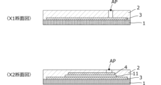
- FIG. 10 is a cross-sectional view in a state where the planar conductor 5B and the planar conductor connection conductor 7B are formed.
- FIG. 11 is a cross-sectional view in a state where the inductor via conductor 6 and the planar conductor connection conductor 7C are formed.
- FIG. 12 is a cross-sectional view in a state where the planar conductor 5A and terminal electrodes 9A and 9B are formed.
- FIG. 13 is a cross-sectional view of the terminal electrodes 10A and 10B formed thereon.
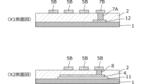
- FIG. 14 is a diagram showing the structure of an electronic component 103 according to the third embodiment.
- FIG. 15 is a cross-sectional view of a state in which the substrate conductive electrode 12, dielectric layer 11, planar conductor 4, etc. are formed.
- FIG. 16 is a cross-sectional view in a state where the planar conductor 5B and the planar conductor connection conductor 7B are formed.
- FIG. 17 is a cross-sectional view in a state where the inductor via conductor 6 and the planar conductor connection conductor 7C are formed.
- FIG. 18 is a cross-sectional view in a state where the planar conductor 5A and terminal electrodes 9A and 9B are formed.
- FIG. 19 is a cross-sectional view in a state where terminal electrodes 10A and 10B are formed.
- FIG. 20 is a diagram showing the structure of an electronic component 104 according to the fourth embodiment.
- FIG. 1 is a diagram showing the structure of an electronic component 101 according to the first embodiment.
- ⁇ Plan view> in FIG. 1 is a plan view of the electronic component 101.
- the ⁇ X1 cross-sectional view> in FIG. 1 is a cross-sectional view taken along the X1-X1 section in the top view of the electronic component 101, and the ⁇ X2 cross-sectional view> in FIG. FIG.
- ⁇ Y1 sectional view> in FIG. 1 is a sectional view taken along Y1-Y1 in the plan view of the electronic component 101, and ⁇ Y2 sectional view> in FIG. FIG.
- the electronic component 101 includes a substrate 1, an insulator layer 2 formed along the surface of the substrate 1, and an inductor formed within the insulator layer 2. Further, conductors 7A, 7B, and 7C for connecting planar conductors are formed on the substrate 1 and conductive to the planar conductor 3 extending along the substrate 1, and planar conductors 7A, 7B, and 7C are formed on the substrate 1 and conductive to the planar conductor 4 extending along the substrate 1. A connecting conductor 8 is provided.
- the inductor includes a plurality of planar conductors 5A, 5B each extending in a plurality of layers (two layers in this example) along the surface of the substrate 1, and a plurality of planar conductors 5A, 5B extending in different layers among the plurality of layers.
- a plurality of inductor via conductors 6 to be connected are provided.
- the inductor is a helical coil inductor having a winding axis WA along the surface of the substrate 1.
- planar conductor connecting conductors 7A, 7B, 7C, and 8 are located at the ends of the helical coil in the direction of the winding axis (the coil opening of the helical coil).
- planar conductors 3 and 4 are capacitor electrodes. That is, a capacitor is constituted by the planar conductors 3 and 4 and the dielectric layer 11 sandwiched between these planar conductors 3 and 4.
- planar conductors 3 and 4 are formed closer to the substrate 1 than the plurality of planar conductors 5A and 5B.
- an inductor formed by a helical coil formed of a plurality of planar conductors 5A, 5B and a plurality of inductor via conductors 6 is located near the terminal electrodes 9A, 9B. Therefore, the path from the circuit to the inductor can be minimized, and the Q value of the inductor can be kept high. Furthermore, space can be saved by arranging the capacitor electrode overlapping the coil forming region.
- the direction of current flowing through the inductor via conductor 6 adjacent to the planar conductor connecting conductors 7A, 7B, and 7C, and the direction of the current flowing through the planar conductor connecting conductors 7A, 7B, and 7C. are the opposite of each other. Further, the direction of the current flowing through the inductor via conductor 6 adjacent to the planar conductor connecting conductor 8 and the direction of the current flowing through the planar conductor connecting conductor 8 are opposite to each other. This will be explained later with reference to FIGS. 3(A), 3(B), etc.
- the substrate 1 is, for example, a silicon substrate, and a planar conductor 3 made of a thin film of polysilicon, Al, or the like is formed on the surface of the substrate 1.
- a dielectric layer 11 made of SiO 2 , SiN, etc. is formed in a predetermined region on the upper surface of the planar conductor 3 .
- a planar conductor 4 made of a thin film of polysilicon, Al, or the like is formed.
- a planar conductor 5A and terminal electrodes 9A and 9B are formed on the surface of the insulator layer 2.
- the planar conductor 3 is electrically connected to the terminal electrode 9B through the planar conductor connecting conductors 7A, 7B, and 7C.
- the planar conductor 4 is electrically connected to the planar conductor 5B through the planar conductor connecting conductor 8.
- the planar conductor connecting conductor is composed of three parts: the planar conductor connecting conductors 7A, 7B, and 7C.
- the planar conductor connection conductor 7B is formed in the same layer as the planar conductor 5B.
- the planar conductor connecting conductor 7B is formed. Therefore, the direction of the current flowing through the inductor via conductor 6 adjacent to the planar conductors 5A and 5B among the plurality of inductor via conductors 6 and the direction of the current flowing through the planar conductor connecting conductor 7C are set to be opposite to each other. There is no need for a process to form a special conductor pattern.
- this electronic component 101 functions as an LC composite component consisting of a series circuit of an inductor and a capacitor.
- the planar conductors 5A, 5B and the inductor via conductor 6 constitute a helical coil inductor L1.
- a capacitor C is constituted by the planar conductors 3 and 4 and the dielectric layer 11 sandwiched between the planar conductors 3 and 4.
- the inductor L2 is constituted by the planar conductor connecting conductors 7A, 7B, 7C, 8, etc.
- the electronic component 101 functions as an LCR composite component consisting of a series circuit of an inductor, a capacitor, and a resistive element.
- An electronic component in which an inductor and a capacitor are connected in series in this way can be used as a frequency filter or an impedance matching circuit.
- FIG. 3B is a plan view showing the positional relationship between an electronic component 301 as a comparative example and a member 201 such as another electronic component adjacent thereto.
- the direction of the magnetic flux around the upper inductor via conductor 6 is the same (right-handed rotation) as shown in FIG. 3(B).
- the direction of the magnetic flux around the lower inductor via conductor 6 is the same (left rotation). Therefore, the overall magnetic flux ⁇ (thick broken line) generated inside and outside the helical coil is greatly expanded.
- FIG. 3(A) is a plan view showing the positional relationship between the electronic component 101 according to this embodiment and another member 201 adjacent thereto.
- the concentric circles with broken lines in the figure indicate the magnetic flux generated in the inductor via conductor 6, the planar conductor connecting conductor 7C, and the like.
- the overall magnetic flux ⁇ generated inside and outside the helical coil is shown by a thick line.
- the inductor via conductors adjacent to the planar conductor connecting conductors 7A, 7B, and 7C are opposite to each other. This suppresses the spread of the magnetic flux ⁇ compared to the example shown in FIG. 3(B). Therefore, even if the member 201 is adjacent to the electronic component 101, there is little mutual influence.
- the inductor via conductor adjacent to the planar conductor connecting conductor 8 (the rightmost inductor via conductor 6 of the lower two inductor via conductors 6 in the direction shown in FIG. 3A)
- the direction of the current flowing through the via conductor 6) and the direction of the current flowing through the planar conductor connecting conductor 8 are opposite to each other. Therefore, the effect of suppressing the spread of the magnetic flux ⁇ is high.
- the spread of the magnetic flux ⁇ is large, but in the electronic component 101 of the present embodiment, the spread of the magnetic flux ⁇ is suppressed, so the distance d1 between the electronic component 101 and the member 201 is It can be made smaller than the distance d2 shown in 3(B).
- FIG. 4(B) is a plan view of an electronic component 311 as a comparative example, which includes the helical coil and another member 21 in the electronic component.
- the structure of the helical coil in this electronic component 311 is as shown in FIG. 3(B).
- FIG. 4(A) is a plan view of the electronic component 111 according to this embodiment.
- This electronic component 311 includes the helical coil and the other member 21 within the electronic component.
- the structure of the helical coil in this electronic component 111 is as shown in FIG. 3(A).
- the spread of the magnetic flux ⁇ is large, but in the electronic component 111 of the present embodiment, the spread of the magnetic flux ⁇ is suppressed.
- the distance can be made smaller than the distance d2, and a small electronic component 111 can be configured.
- the inductor via conductors 6 are arranged in two rows, and the planar conductor connecting conductors 7A, 7B, and 7C are lined up at the end of one row of the two rows of inductor via conductors 6.
- the planar conductor connecting conductors 8 are located side by side at the end of the other row
- the number of inductor via conductors 6 is not limited to two rows. Further, even if the planar conductor connecting conductors 8 are not located in line with the ends of all the rows, there is an effect of suppressing the spread of the magnetic flux ⁇ .
- the ends of the inductor via conductors 6 and the planar conductor connecting conductors 7A, 7B, 7C are or 8 is an equal interval, but it is not essential that this interval is an equal interval.
- this interval is too close, the magnetic fields caused by the helical coil will be weakened, resulting in a decrease in the inductance of the inductor formed by the helical coil.
- the above-mentioned intervals are preferably about equal intervals.
- planar conductors 3 and 4 are formed on the substrate 1, but the planar conductors 3 and 4 may be formed in the intermediate layer of the insulator layer 2.
- eddy currents may be generated in the planar conductors 3 and 4 due to the high frequency magnetic field generated by the helical coil.
- the spread of the magnetic flux ⁇ is suppressed, so the loss due to the eddy current (Q value of the inductor) is suppressed. deterioration) is suppressed.
- the planar conductor 3 is formed not only in the capacitor forming portion but also over almost the entire surface of the substrate 1. Therefore, there is electromagnetic shielding for the members and circuits below the substrate 1.
- FIG. 5 is a diagram showing the structure of the electronic component 102 according to the second embodiment.
- ⁇ Plan view> in FIG. 5 is a plan view of the electronic component 102.
- ⁇ X1 sectional view> in FIG. 5 is a sectional view taken along the line X1-X1 in the plan view of the electronic component 102, and ⁇ X2 sectional view> in FIG. FIG.
- the electronic component 102 includes a substrate 1, an insulator layer 2 formed along the surface of the substrate 1, an inductor formed in the insulator layer 2, and a surface formed on the substrate 1 and extending along the substrate 1. It includes conductors 3 and 4, conductors 7A, 7B, and 7C for connecting planar conductors that are electrically connected to the planar conductor 3, and conductor 8 for connecting planar conductors that is electrically connected to the planar conductor 4.
- Terminal electrodes 10A and 10B are formed on the surface of the insulator layer 2. Terminal electrodes 10A and 10B are electrically connected to terminal electrodes 9A and 9B.
- the planar conductors 5A and 5B were exposed together with the terminal electrodes 9A and 9B, but in the electronic component 102 shown in the data of the second embodiment, Only the terminal electrodes 10A and 10B are exposed. The other configurations are as shown in the first embodiment.
- FIG. 6 is a cross-sectional view of a state in which the planar conductor 3 is formed.
- the substrate 1 is a silicon intrinsic semiconductor substrate or a silicon impurity semiconductor substrate, and in this step, an Al film or a Cu film is deposited on the surface of the substrate 1 and lifted off, an Al film or a Cu film is formed by sputtering or CVD, It is formed by semiconductor processes such as lithography and etching.
- FIG. 7 is a cross-sectional view with the dielectric layer 11 formed.
- a dielectric layer 11 such as an SiO 2 film or a SiN film is formed on the surface of the planar conductor 3 by a semiconductor process such as sputtering or CVD, and then a pattern of the dielectric layer 11 is formed by lithography and etching. .
- FIG. 8 is a cross-sectional view of the sheet conductor 4 after it has been formed.
- the semiconductor material includes steps such as depositing an Al film or Cu film and lift-off, depositing an Al film or Cu film by sputtering or CVD, lithography, and etching.
- a pattern of planar conductors 4 is formed by a process.
- FIG. 9 is a cross-sectional view with the insulator layer 2 formed.
- a resin (organic) film, an SiO 2 film, an SiN film, or other inorganic film is formed by a method such as spin coating, CVD, or sputtering, and then an opening AP is formed at a predetermined location by lithography and etching.
- FIG. 10 is a cross-sectional view in a state where the planar conductor 5B and the planar conductor connection conductor 7B are formed.
- the conductors 7A and 8 for connecting planar conductors are formed in the opening AP shown in FIG. 9, and the planar conductor 5B and the conductor 7B for connecting planar conductors are formed on the surface of the insulating layer 2.
- it is formed by depositing Cu, lithography, and plating, or by sputtering, lithography, and etching Cu, or by lithography, vapor deposition, and lift-off of Cu. .
- FIG. 11 is a cross-sectional view in a state where the inductor via conductor 6 and the planar conductor connection conductor 7C are formed.
- the pattern of the planar conductor 4 is formed by a semiconductor process such as depositing an Al film or a Cu film, lifting off, depositing an Al film or a Cu film by sputtering or CVD, lithography, and etching. .
- FIG. 12 is a cross-sectional view with the planar conductor 5A and terminal electrodes 9A and 9B formed.
- a planar conductor 5A and terminal electrodes 9A and 9B are formed on the surface of the insulator layer 2. For example, it is formed by depositing Cu, lithography, and plating, or by sputtering, lithography, and etching Cu, or by lithography, vapor deposition, and lift-off of Cu. .
- FIG. 13 is a cross-sectional view with terminal electrodes 10A and 10B formed.
- the terminal electrodes 10A, 10B are electrodes for mounting, and are formed by applying Ni plating, Au plating, etc. to the surfaces of the terminal electrodes 9A, 9B.
- a protective film is formed, and the terminal electrodes 10A and 10B are opened to expose the terminal electrodes 10A and 10B.
- the insulator layer 2 may be composed of a plurality of types of layers, and if all the layers are made of the same material, the boundaries may not be visible after completion as shown in FIG. 13.
- FIG. 14 is a diagram showing the structure of an electronic component 103 according to the third embodiment.
- ⁇ Plan view> in FIG. 14 is a plan view of the electronic component 103.
- ⁇ X1 sectional view> in FIG. 14 is a sectional view taken along the line X1-X1 in the plan view of the electronic component 103, and ⁇ X2 sectional view> in FIG. FIG.
- the electronic component 103 includes a substrate 1 , an insulator layer 2 formed along the surface of the substrate 1 , an inductor formed in the insulator layer 2 , and a surface formed on the substrate 1 and extending along the substrate 1 .
- the conductor 4 includes a planar conductor 4, conductors 7A, 7B, and 7C for connecting planar conductors that are electrically connected to the planar conductor 4, and a conductor 8 for connecting planar conductors that is electrically connected to the planar conductor 4.
- a dielectric layer 11 is formed on the surface of the substrate 1.
- a planar conductor 4 is formed on the surface of this dielectric layer 11.
- a substrate conduction electrode 12 is formed at a predetermined position on the surface of the substrate 1.
- the substrate 1 is a semiconductor substrate with high conductivity, or a semiconductor substrate on which a layer with high conductivity is formed on the surface on which each of the above layers is formed.
- the other configurations are as shown in the second embodiment.
- FIG. 15 is a cross-sectional view of a state in which the substrate conductive electrode 12, dielectric layer 11, planar conductor 4, etc. are formed.
- the substrate 1 is a silicon impurity semiconductor substrate.
- a dielectric layer 11 such as a SiO 2 film or a SiN film is formed on the surface of the substrate 1 by a semiconductor process such as sputtering or CVD, and then the dielectric layer 11 is formed by lithography and etching. form a pattern.
- FIG. 16 is a cross-sectional view in a state where the planar conductor 5B and the planar conductor connection conductor 7B are formed.
- FIG. 17 is a cross-sectional view in a state where the inductor via conductor 6 and the planar conductor connection conductor 7C are formed.
- FIG. 18 is a cross-sectional view in a state where the planar conductor 5A and terminal electrodes 9A and 9B are formed.
- FIG. 19 is a cross-sectional view in a state where terminal electrodes 10A and 10B are formed.
- FIGS. 16 to 19 are the same as the steps shown in FIGS. 10 to 13 in the second embodiment.
- the present invention can also be applied when the substrate is used as part of a planar conductor for a capacitor.
- FIG. 20 is a diagram showing the structure of an electronic component 104 according to the fourth embodiment.
- ⁇ Plan view> in FIG. 20 is a plan view of the electronic component 104.
- ⁇ X1 sectional view> in FIG. 20 is a sectional view taken along the line X1-X1 in the plan view of the electronic component 104, and ⁇ X2 sectional view> in FIG. FIG.
- the substrate 1 is a P-type silicon semiconductor substrate, and an N well 13 is formed at a predetermined location on the substrate 1, and a P+ region 14 is formed in a predetermined region within the N well.
- the substrate conduction electrode 12 is formed on the surface of the N well 13 region. Further, the substrate conduction electrode 15 is formed on the surface of the P+ region.
- a diode is configured by the N well 13, the substrate conductive electrode 12 electrically connected to the N well 13, the P+ region 14, and the substrate conductive electrode 15 electrically conductive to the P+ region.
- the electronic component 104 acts as an electronic component in which a diode is connected in series to an inductor formed by a helical coil.
- a diode is connected in series to an inductor formed by a helical coil.
- it can be used as an ESD protection element.
- a diode is configured on the substrate 1, but a transistor may be configured in a similar manner.
- a substrate an insulator layer formed along the surface of the substrate, an inductor formed in the insulator layer, and an inductor formed in the substrate or the insulator layer and extending along the substrate.
- the inductor includes a plurality of planar conductors each extending in a plurality of layers along the surface of the substrate, and a plurality of inductor via conductors that connect the planar conductors extending in different layers among the plurality of layers.
- an inductor using a helical coil having a winding axis along the surface of the substrate an inductor using a helical coil having a winding axis along the surface of the substrate, The direction of current flowing through the inductor via conductor adjacent to the planar conductor connecting conductor among the plurality of inductor via conductors is opposite to the direction of the current flowing through the planar conductor connecting conductor, electronic components.
- planar conductor connecting conductor is located at an end of the helical coil in the direction of the winding axis (coil opening of the helical coil inductor).
- ⁇ 3> The electronic component according to ⁇ 1> or ⁇ 2>, wherein the planar conductor is formed closer to the substrate than the plurality of planar conductors.
- planar conductor connecting conductor is composed of three or more parts, one of which is formed in the same layer as the planar conductor.
- ⁇ 5> The electronic component according to any one of ⁇ 1> to ⁇ 4>, wherein the substrate is a low-resistance semiconductor substrate, and the planar conductor is a capacitor electrode that forms a capacitor together with the semiconductor substrate.
- ⁇ 6> The electronic component according to any one of ⁇ 1> to ⁇ 5>, wherein the planar conductor is a resistor film.
- ⁇ 7> The electronic component according to any one of ⁇ 1> to ⁇ 6>, wherein the substrate is a semiconductor substrate, and the planar conductor constitutes a semiconductor element together with the semiconductor substrate.
- ⁇ 8> Any one of ⁇ 1> to ⁇ 7>, wherein the inductor via conductors are arranged in two rows, and the planar conductor connecting conductor is located alongside the ends of the two rows of inductor via conductors. Electronic components listed in .
Landscapes
- Engineering & Computer Science (AREA)
- Power Engineering (AREA)
- Microelectronics & Electronic Packaging (AREA)
- Coils Or Transformers For Communication (AREA)
Priority Applications (3)
| Application Number | Priority Date | Filing Date | Title |
|---|---|---|---|
| CN202380046805.7A CN119384882A (zh) | 2022-06-30 | 2023-06-27 | 电子部件 |
| JP2024530856A JPWO2024004985A1 (https=) | 2022-06-30 | 2023-06-27 | |
| US18/987,891 US20250118659A1 (en) | 2022-06-30 | 2024-12-19 | Electronic component |
Applications Claiming Priority (2)
| Application Number | Priority Date | Filing Date | Title |
|---|---|---|---|
| JP2022-105968 | 2022-06-30 | ||
| JP2022105968 | 2022-06-30 |
Related Child Applications (1)
| Application Number | Title | Priority Date | Filing Date |
|---|---|---|---|
| US18/987,891 Continuation US20250118659A1 (en) | 2022-06-30 | 2024-12-19 | Electronic component |
Publications (1)
| Publication Number | Publication Date |
|---|---|
| WO2024004985A1 true WO2024004985A1 (ja) | 2024-01-04 |
Family
ID=89383083
Family Applications (1)
| Application Number | Title | Priority Date | Filing Date |
|---|---|---|---|
| PCT/JP2023/023730 Ceased WO2024004985A1 (ja) | 2022-06-30 | 2023-06-27 | 電子部品 |
Country Status (4)
| Country | Link |
|---|---|
| US (1) | US20250118659A1 (https=) |
| JP (1) | JPWO2024004985A1 (https=) |
| CN (1) | CN119384882A (https=) |
| WO (1) | WO2024004985A1 (https=) |
Citations (3)
| Publication number | Priority date | Publication date | Assignee | Title |
|---|---|---|---|---|
| US5070317A (en) * | 1989-01-17 | 1991-12-03 | Bhagat Jayant K | Miniature inductor for integrated circuits and devices |
| JP2001223334A (ja) * | 2000-02-09 | 2001-08-17 | Toshiba Corp | 半導体装置製造方法および半導体装置 |
| WO2007138857A1 (ja) * | 2006-06-01 | 2007-12-06 | Murata Manufacturing Co., Ltd. | 無線icデバイス及び無線icデバイス用複合部品 |
Family Cites Families (5)
| Publication number | Priority date | Publication date | Assignee | Title |
|---|---|---|---|---|
| JP2004103756A (ja) * | 2002-09-09 | 2004-04-02 | Tdk Corp | コイル部品およびその製造方法 |
| US9954267B2 (en) * | 2015-12-28 | 2018-04-24 | Qualcomm Incorporated | Multiplexer design using a 2D passive on glass filter integrated with a 3D through glass via filter |
| CN107710605B (zh) * | 2016-06-06 | 2021-06-15 | 华为技术有限公司 | 互感耦合滤波器及无线保真WiFi模组 |
| JP2021197454A (ja) * | 2020-06-15 | 2021-12-27 | イビデン株式会社 | 配線基板及び配線基板の製造方法 |
| CN116420201A (zh) * | 2020-11-06 | 2023-07-11 | 株式会社村田制作所 | 滤波器装置以及搭载有该滤波器装置的高频前端电路 |
-
2023
- 2023-06-27 JP JP2024530856A patent/JPWO2024004985A1/ja active Pending
- 2023-06-27 WO PCT/JP2023/023730 patent/WO2024004985A1/ja not_active Ceased
- 2023-06-27 CN CN202380046805.7A patent/CN119384882A/zh active Pending
-
2024
- 2024-12-19 US US18/987,891 patent/US20250118659A1/en active Pending
Patent Citations (3)
| Publication number | Priority date | Publication date | Assignee | Title |
|---|---|---|---|---|
| US5070317A (en) * | 1989-01-17 | 1991-12-03 | Bhagat Jayant K | Miniature inductor for integrated circuits and devices |
| JP2001223334A (ja) * | 2000-02-09 | 2001-08-17 | Toshiba Corp | 半導体装置製造方法および半導体装置 |
| WO2007138857A1 (ja) * | 2006-06-01 | 2007-12-06 | Murata Manufacturing Co., Ltd. | 無線icデバイス及び無線icデバイス用複合部品 |
Also Published As
| Publication number | Publication date |
|---|---|
| JPWO2024004985A1 (https=) | 2024-01-04 |
| CN119384882A (zh) | 2025-01-28 |
| US20250118659A1 (en) | 2025-04-10 |
Similar Documents
| Publication | Publication Date | Title |
|---|---|---|
| US8050045B2 (en) | Electronic component and method of manufacturing the same | |
| JP4866952B2 (ja) | 複合電子部品 | |
| JP4749482B2 (ja) | 複合電子部品 | |
| US7508292B2 (en) | Coil component | |
| US7408435B2 (en) | Coil component | |
| US7064629B2 (en) | Thin-film common mode filter and thin-film common mode filter array | |
| TWI395240B (zh) | 積體半導體電感器及其形成方法與積體半導體濾波器 | |
| US7002446B2 (en) | Coil component | |
| US7023299B2 (en) | Thin-film common mode filter and thin-film common mode filter array | |
| US10770451B2 (en) | Thin-film ESD protection device | |
| JP5382091B2 (ja) | 複合電子部品 | |
| US11469593B2 (en) | Thin-film ESD protection device with compact size | |
| CN110959188A (zh) | 电容器 | |
| US20130271251A1 (en) | Substrate-Less Electronic Component | |
| JP6788847B2 (ja) | キャパシタ | |
| TWI390705B (zh) | 用於被動積體裝置之靜電放電保護 | |
| JP7758199B2 (ja) | 電子部品 | |
| WO2024004985A1 (ja) | 電子部品 | |
| JP2009266908A (ja) | 半導体装置の製造方法、及び半導体装置 | |
| JP2009033033A (ja) | コモンモードチョークコイル及びその製造方法 | |
| WO2025052920A1 (ja) | 受動電子部品 | |
| JP2002359115A (ja) | チップ型コモンモードチョークコイル | |
| US20260059668A1 (en) | Functional substrate and method for manufacturing the same, and electronic device | |
| WO2023181806A1 (ja) | 電子部品 | |
| JP2000021635A (ja) | スパイラルインダクタおよびそれを用いた集積回路 |
Legal Events
| Date | Code | Title | Description |
|---|---|---|---|
| 121 | Ep: the epo has been informed by wipo that ep was designated in this application |
Ref document number: 23831425 Country of ref document: EP Kind code of ref document: A1 |
|
| WWE | Wipo information: entry into national phase |
Ref document number: 2024530856 Country of ref document: JP |
|
| WWE | Wipo information: entry into national phase |
Ref document number: 202380046805.7 Country of ref document: CN |
|
| WWP | Wipo information: published in national office |
Ref document number: 202380046805.7 Country of ref document: CN |
|
| NENP | Non-entry into the national phase |
Ref country code: DE |
|
| 122 | Ep: pct application non-entry in european phase |
Ref document number: 23831425 Country of ref document: EP Kind code of ref document: A1 |