WO2024004392A1 - 積層セラミックコンデンサ - Google Patents
積層セラミックコンデンサ Download PDFInfo
- Publication number
- WO2024004392A1 WO2024004392A1 PCT/JP2023/017694 JP2023017694W WO2024004392A1 WO 2024004392 A1 WO2024004392 A1 WO 2024004392A1 JP 2023017694 W JP2023017694 W JP 2023017694W WO 2024004392 A1 WO2024004392 A1 WO 2024004392A1
- Authority
- WO
- WIPO (PCT)
- Prior art keywords
- ceramic
- ionic radius
- internal electrode
- internal electrodes
- abo
- Prior art date
Links
- 239000003985 ceramic capacitor Substances 0.000 title claims abstract description 33
- 239000000919 ceramic Substances 0.000 claims abstract description 78
- 229910052709 silver Inorganic materials 0.000 claims abstract description 36
- 239000004332 silver Substances 0.000 claims abstract description 35
- 229910002367 SrTiO Inorganic materials 0.000 claims description 17
- 239000000843 powder Substances 0.000 description 67
- BQCADISMDOOEFD-UHFFFAOYSA-N Silver Chemical compound [Ag] BQCADISMDOOEFD-UHFFFAOYSA-N 0.000 description 36
- 239000002002 slurry Substances 0.000 description 24
- 229910052751 metal Inorganic materials 0.000 description 20
- 239000002184 metal Substances 0.000 description 20
- 150000002500 ions Chemical class 0.000 description 18
- 239000002994 raw material Substances 0.000 description 17
- 239000003960 organic solvent Substances 0.000 description 12
- 239000002270 dispersing agent Substances 0.000 description 11
- 239000002923 metal particle Substances 0.000 description 11
- 238000000034 method Methods 0.000 description 10
- 238000002360 preparation method Methods 0.000 description 9
- 238000011156 evaluation Methods 0.000 description 8
- UODXCYZDMHPIJE-UHFFFAOYSA-N menthanol Chemical compound CC1CCC(C(C)(C)O)CC1 UODXCYZDMHPIJE-UHFFFAOYSA-N 0.000 description 8
- 239000000203 mixture Substances 0.000 description 8
- 239000000463 material Substances 0.000 description 7
- 238000002156 mixing Methods 0.000 description 7
- 239000011347 resin Substances 0.000 description 6
- 229920005989 resin Polymers 0.000 description 6
- 238000010304 firing Methods 0.000 description 4
- 238000005245 sintering Methods 0.000 description 4
- 229910004298 SiO 2 Inorganic materials 0.000 description 3
- 229910052788 barium Inorganic materials 0.000 description 3
- 229910052791 calcium Inorganic materials 0.000 description 3
- 238000007606 doctor blade method Methods 0.000 description 3
- 238000002474 experimental method Methods 0.000 description 3
- 239000007858 starting material Substances 0.000 description 3
- 229910052712 strontium Inorganic materials 0.000 description 3
- 229910052692 Dysprosium Inorganic materials 0.000 description 2
- 239000001856 Ethyl cellulose Substances 0.000 description 2
- ZZSNKZQZMQGXPY-UHFFFAOYSA-N Ethyl cellulose Chemical compound CCOCC1OC(OC)C(OCC)C(OCC)C1OC1C(O)C(O)C(OC)C(CO)O1 ZZSNKZQZMQGXPY-UHFFFAOYSA-N 0.000 description 2
- 229910052688 Gadolinium Inorganic materials 0.000 description 2
- 229910010413 TiO 2 Inorganic materials 0.000 description 2
- 229920006318 anionic polymer Polymers 0.000 description 2
- 229910010293 ceramic material Inorganic materials 0.000 description 2
- 239000013078 crystal Substances 0.000 description 2
- 229920001249 ethyl cellulose Polymers 0.000 description 2
- 235000019325 ethyl cellulose Nutrition 0.000 description 2
- 229910052749 magnesium Inorganic materials 0.000 description 2
- 229910052748 manganese Inorganic materials 0.000 description 2
- 238000004519 manufacturing process Methods 0.000 description 2
- 238000007747 plating Methods 0.000 description 2
- 229910052710 silicon Inorganic materials 0.000 description 2
- 238000003756 stirring Methods 0.000 description 2
- 229910052727 yttrium Inorganic materials 0.000 description 2
- 150000001450 anions Chemical class 0.000 description 1
- 229910002113 barium titanate Inorganic materials 0.000 description 1
- 229910052796 boron Inorganic materials 0.000 description 1
- 238000006243 chemical reaction Methods 0.000 description 1
- 229910052802 copper Inorganic materials 0.000 description 1
- 230000006866 deterioration Effects 0.000 description 1
- 239000006185 dispersion Substances 0.000 description 1
- 230000005684 electric field Effects 0.000 description 1
- 239000002245 particle Substances 0.000 description 1
- 229920000642 polymer Polymers 0.000 description 1
- 238000007639 printing Methods 0.000 description 1
- 238000007650 screen-printing Methods 0.000 description 1
- 229910052708 sodium Inorganic materials 0.000 description 1
- 229910052726 zirconium Inorganic materials 0.000 description 1
Images
Classifications
-
- H—ELECTRICITY
- H01—ELECTRIC ELEMENTS
- H01G—CAPACITORS; CAPACITORS, RECTIFIERS, DETECTORS, SWITCHING DEVICES, LIGHT-SENSITIVE OR TEMPERATURE-SENSITIVE DEVICES OF THE ELECTROLYTIC TYPE
- H01G4/00—Fixed capacitors; Processes of their manufacture
- H01G4/30—Stacked capacitors
Definitions
- the present invention relates to a multilayer ceramic capacitor, and particularly to the composition of internal electrodes provided in the multilayer ceramic capacitor.
- a multilayer ceramic capacitor typically includes a multilayer body and a multilayer structure including a plurality of laminated dielectric layers made of ceramic and a plurality of internal electrodes each disposed along a plurality of interfaces between the dielectric layers.
- a plurality of external electrodes are provided on the outer surface and electrically connected to the internal electrodes.
- the internal electrode includes a plurality of first internal electrodes and a plurality of second internal electrodes arranged alternately in the stacking direction of the laminate, and the external electrode includes a first external electrode electrically connected to the first internal electrode. and a second external electrode electrically connected to the second internal electrode.
- the temperature at which the conductive metal particles contained in the conductive paste film, which will become the internal electrodes, is sintered is higher than the temperature at which the ceramic constituting the dielectric layer is sintered. Since the temperature is low, the metal particles contained in the internal electrodes are sintered first. This causes a reduction in the coverage of the internal electrodes. Particularly, in the case of internal electrodes that are thinner, such as having a thickness of 1 ⁇ m or less, the coverage tends to decrease, and such a decrease in coverage tends to hinder an increase in capacity.
- the temperature at which the conductive metal particles contained in the conductive paste film that will become the internal electrodes is sintered must be needs to be higher.
- the temperature at which the metal particles contained in the conductive paste film, which is to become the internal electrode, sinter can be brought closer to the temperature at which the ceramic forming the dielectric layer starts sintering, and the internal electrode and dielectric layer The shrinkage timing during sintering can be brought closer to each other. As a result, the coverage of the internal electrodes becomes high, and a large capacity can be realized.
- Patent Document 1 Japanese Unexamined Patent Publication No. 2016-318057
- a ceramic material having a composition similar to that of the ceramic constituting the dielectric layer that is, a co-material
- co-material By adding the co-material, it is possible to shift the sintering timing of the metal particles contained in the conductive paste film that will become the internal electrode to a higher temperature side, and the metal particles contained in the conductive paste film are sintered.
- the temperature can be brought close to the temperature at which the ceramic forming the dielectric layer is sintered.
- an object of the present invention is to provide a multilayer ceramic capacitor including internal electrodes that can maintain relatively high coverage even when the layers are thinned.
- a multilayer ceramic capacitor according to the present invention includes a multilayer body including a plurality of stacked dielectric layers made of ceramic and a plurality of internal electrodes respectively arranged along a plurality of interfaces between the dielectric layers.
- the present invention is characterized in that the internal electrode contains silver as a conductive component and at least one selected from AgTiO 3 , EuTiO 3 and NaTiO 3 .
- At least one selected from AgTiO 3 , EuTiO 3 and NaTiO 3 contained in the internal electrode contributes to increasing the coverage of the internal electrode containing silver as a conductive component. Therefore, even if the internal electrodes are made thinner, the coverage of the internal electrodes does not decrease, and it is possible to prevent an increase in the capacity of the multilayer ceramic capacitor from being hindered.
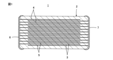
- FIG. 1 is a cross-sectional view schematically showing a multilayer ceramic capacitor 1 according to an embodiment of the present invention.
- the multilayer ceramic capacitor 1 includes a multilayer body 2.
- the laminate 2 includes a plurality of stacked dielectric layers 3 made of ceramic, and a plurality of internal electrodes 4 and 5 arranged along the interface between the plurality of dielectric layers 3.
- the internal electrodes 4 and 5 are classified into a plurality of first internal electrodes 4 and a plurality of second internal electrodes 5, which are alternately arranged in the stacking direction of the laminate 3.
- a first external electrode 6 and a second external electrode 7 are provided on the outer surface of the laminate 2, more specifically, on each opposing end surface.
- the first external electrode 6 is electrically connected to the first internal electrode 4
- the second external electrode 7 is electrically connected to the second internal electrode 5 .
- the dielectric layer 3 is made of, for example, a ceramic whose main component is ABO 3 (A is at least one of Ba, Ca, and Sr, and B is at least one of Ti and Zr). Become. Further, the ceramic may have the above-mentioned ABO 3 as a main component, and may further contain at least one of Mn, Mg, Si, Y, Dy, and Gd as a subcomponent.
- Internal electrodes 4 and 5 contain silver as a conductive component. Furthermore, as a characteristic composition, the internal electrodes 4 and 5 contain at least one selected from AgTiO 3 , EuTiO 3 and NaTiO 3 . AgTiO 3 , EuTiO 3 and NaTiO 3 have an illuminite crystal structure.
- the dielectric layer 3 is made of a ceramic whose main component is at least one selected from BaTiO 3 , SrTiO 3 and CaZrO 3 , and the internal electrodes 4 and 5 contains silver as a conductive component, contains at least one selected from AgTiO 3 , EuTiO 3 and NaTiO 3 as a ceramic material, and optionally contains BaTiO 3 , SrTiO 3 and CaZrO contained in the dielectric layer 3. It further contains at least one species selected from 3 .
- the external electrodes 6 and 7 are formed, for example, by applying a conductive paste containing Ag or Cu as a main conductive component to the end surface of the laminate 2 and baking it. If necessary, for example, Ni plating and Sn plating may be applied on the thick film formed by baking.
- the multilayer ceramic capacitor 1 is manufactured, for example, through the following steps. First, a ceramic slurry containing ceramic raw material powder having the composition as described above is prepared. Next, a suitable sheet forming method is applied to the ceramic slurry to form a ceramic green sheet. Next, a conductive paste to become each of the internal electrodes 4 and 5 is applied by printing or the like onto a predetermined ceramic green sheet among the plurality of ceramic green sheets. Next, a plurality of ceramic green sheets are laminated and then pressed together to obtain a green laminate. The green laminate is then fired. In this firing process, the ceramic green sheet becomes the dielectric layer 3. Thereafter, external electrodes 6 and 7 are formed on the end faces of the laminate 3.
- the conductive paste to become the internal electrodes 4 and 5 used in manufacturing the multilayer ceramic capacitor 1 described above is preferably produced as follows.
- the first step is to prepare a ceramic powder slurry containing ceramic powder, an organic solvent, and a dispersant
- the second step is to prepare a metal powder slurry containing a conductive metal powder, an organic solvent, and a dispersant.
- a third step of preparing an organic vehicle containing an organic resin component and an organic solvent is to prepare a fourth step of mixing the ceramic powder slurry, metal powder slurry, and organic vehicle.
- a ceramic powder slurry is prepared by mixing ceramic powder and a dispersant into an organic solvent.
- the ceramic powder used is, for example, at least one selected from AgTiO 3 , EuTiO 3 and NaTiO 3 as ABO trioxides, and in addition to this, BaTiO 3 and SrTiO 3 as co-materials. 3 and at least one selected from CaZrO 3 and CaZrO 3 may be used.
- the conductive metal powder contained in the metal powder slurry produced in the second step described below contains silver, AgTiO 3 , EuTiO 3 and NaTiO 3 as the above-mentioned ABO 3 oxides have a 6-coordination of silver.
- the ceramic powder made of at least one selected from AgTiO 3 , EuTiO 3 and NaTiO 3 as the ABO trioxide
- the ceramic powder has the above-mentioned ABO trioxide as a main component, and may further contain at least one of Mn, Mg, Si, Y, Dy, and Gd as a subcomponent. When such subcomponents are contained, grain growth of ceramic particles is suppressed, and sintering of metal particles may be effectively suppressed.
- an anionic polymer dispersant for example, an anionic polymer dispersant can be used, and as the organic solvent, for example, dihydroterpineol can be used.
- a metal powder slurry is prepared by mixing conductive metal powder and a dispersant into an organic solvent.
- a powder made of silver is used.
- the dispersant and organic solvent used in the second step those similar to those used in the first step can be used.
- an organic vehicle is produced by mixing an organic resin component with an organic solvent.
- the organic resin component for example, ethyl cellulose resin can be used.
- the organic solvent used in the third step can also be the same as that used in the first step.
- the above-described ceramic powder slurry, metal powder slurry, and organic vehicle are mixed.
- a conductive paste to become the internal electrodes 4 and 5 is obtained.
- This conductive paste contains a ceramic powder slurry, and the ceramic powder slurry is a ceramic powder made of at least one selected from AgTiO 3 , EuTiO 3 and NaTiO 3 as an ABO 3 oxide with a specific ionic radius, as described above. Therefore, the internal electrodes 4 and 5 included in the multilayer ceramic capacitor 1 manufactured through the firing process contain at least one selected from AgTiO 3 , EuTiO 3 and NaTiO 3 .
- silver powder was prepared as the conductive metal powder contained in the conductive paste for forming internal electrodes.
- (Experimental example 1) Main component of ceramic constituting dielectric layer: BaTiO 3 1.
- the main component BaCO 3 and TiO 2 powders were weighed, mixed in a ball mill for 72 hours, and then heat treated at a top temperature of 1000°C for 2 hours. A heat-treated powder was obtained.
- MnO, Dy 2 O 3 , MgO, SiO 2 and BaCO 3 powders were prepared as subcomponents, and the subcomponent powders were 100BaTiO 3 +0.5Mn+1.0Dy+1.0Mg+1.0Si+2. The powders were weighed so as to have a composition ratio of 0Ba, and these subcomponent powders were added to the heat-treated powder, mixed for 24 hours in a ball mill, and then dried to obtain a BaTiO 3 ceramic raw material powder.
- the conductive paste for forming internal electrodes contains the "ABO trioxide " powder shown in Table 2 below and the BaTiO 3 ceramic raw material powder for the dielectric layer. It was used as a ceramic powder.
- ABO 3 oxide powders and BaTiO 3 -based ceramic raw material powder were weighed so as to have the "addition ratio" shown in Table 2, and these powders, dihydroterpineol as an organic solvent, and anion as a dispersant were weighed.
- a ceramic powder slurry was prepared by pre-mixing the mixture and the polymer dispersant using a medium-free stirring mill, and then performing a dispersion treatment using a medium-stirring mill (first step).
- silver powder as a conductive metal powder, dihydroterpineol as an organic solvent, and an anionic polymer dispersant as a dispersant were dispersed in a three-roll mill to prepare a metal powder slurry (second process).
- the metal powder slurry and the ceramic powder slurry were added to the organic vehicle and mixed and dispersed to produce a conductive paste for forming internal electrodes (fourth step).
- Table 2 shows the ratio of the 6-coordinate ionic radius of the A-site element to the 6-coordinate ionic radius of silver to be included in the internal electrode, i.e., "ionic radius ratio (A-site element/metallic silver)". "It is shown. For sample 8, the ratio of the ionic radius (1.35 ⁇ ) of Ba element in the 6-coordination shown in Table 1 to the ionic radius (1.15 ⁇ ) in the 6-coordination of silver is shown. .
- Multilayer Ceramic Capacitor A ceramic slurry containing the BaTiO 3 ceramic raw material powder prepared in 1 above was prepared, and then a doctor blade method was applied to the ceramic slurry to form a ceramic green sheet. Next, the conductive paste for forming internal electrodes prepared in 2 above was applied onto a predetermined ceramic green sheet among the plurality of ceramic green sheets by screen printing. Next, a plurality of ceramic green sheets were laminated and pressed together to obtain a green laminate. The green laminate was then fired. Thereafter, external electrodes were formed on the end faces of the sintered laminate to produce a multilayer ceramic capacitor as a sample.
- the internal electrode and dielectric layer located at the center in the height direction of the laminate provided in the multilayer ceramic capacitor serving as a sample were peeled off from each other by electric field peeling.
- the vicinity of the exposed central part of the internal electrode was observed using a microscope at a magnification of 100 times. Then, by analyzing the obtained images, the ratio of the area occupied by the conductive film as the internal electrode in the exposed portion was determined as the "coverage” shown in Table 2. If the “coverage” is 80% or more, it is judged as good, and enter “ ⁇ ” in the “evaluation” column.If the "coverage” is lower than 80%, it is judged as poor, and in the "evaluation” column, write " ⁇ ". ⁇ ” was entered.
- Samples 1 to 3 and 5 to 7 in Table 2 have an “evaluation” of “ ⁇ ”.
- the internal electrode contains one of AgTiO 3 , EuTiO 3 and NaTiO 3 as the ABO 3 oxide. Further, the internal electrode contains silver as a conductive component.
- the ionic radius of silver in six coordinations is 1.15 ⁇ .
- the ionic radius in the 6-coordination of each A-site element of AgTiO 3 , EuTiO 3 and NaTiO 3 as ABO 3 oxides contained in the internal electrodes in Samples 1 to 3 and 5 to 7 is shown in Table 1. , 1.15 ⁇ , 1.17 ⁇ and 1.02 ⁇ , respectively.
- AgTiO 3 , EuTiO 3 and NaTiO 3 as ABO 3 oxides in Samples 1 to 3 and 5 to 7 have an ionic radius in the 6-coordination of the A-site element in ABO 3 that is included in the internal electrode. Since the ionic radius is equal to or close to the six-coordinate ionic radius of silver as a conductive metal, the energy difference with silver in the internal electrode is 0 or small, so it remains without being ejected from the internal electrode part, and the internal It acts to improve the heat resistance of the electrode. As a result, it is estimated that the coverage of Samples 1 to 3 and 5 to 7 was as high as 82% or more.
- the addition ratio of AgTiO 3 , EuTiO 3 and NaTiO 3 is not necessarily 100%, but if it is 10% or more, none of AgTiO 3 , EuTiO 3 and NaTiO 3 is included. The effect of improving coverage was observed compared to the previous case.
- the ratio of the ionic radius of Ba in six coordinations to the ionic radius of silver in six coordinations that is, the "ionic radius ratio” is 1.17. Therefore, the "ion radius ratio” was outside the range of 0.89 or more and 1.02 or less, and the coverage was as low as 75%.
- Example 2 Main component of ceramic constituting dielectric layer: CaZrO 3 1.
- CaZrO 3 -based ceramic raw material constituting the dielectric layer As starting materials, powders of main components CaCO 3 and ZrO 2 and powders of MnO, SiO 2 and MgO as subcomponents were weighed and heated in a ball mill for 72 hours. After mixing, the mixture was heat treated at a top temperature of 1000° C. for 2 hours to obtain a CaZrO 3 ceramic raw material powder.
- the conductive paste for forming internal electrodes contained the "ABO trioxide " powder shown in Table 3 below and the CaZrO 3 -based ceramic raw material powder for the dielectric layer. It was used as a ceramic powder.
- Samples 11 to 13 and 15 to 17 in Table 3 have an “evaluation” of “ ⁇ ”.
- the internal electrodes contained one of AgTiO 3 , EuTiO 3 and NaTiO 3 as the ABO 3 oxide. Further, the internal electrode contains silver as a conductive component.
- the ionic radius of silver in six coordinations is 1.15 ⁇ .
- the ionic radius in the 6-coordination of each A-site element of AgTiO 3 , EuTiO 3 and NaTiO 3 as ABO 3 oxides contained in the internal electrodes in Samples 11 to 13 and 15 to 17 is shown in Table 1. , 1.15 ⁇ , 1.17 ⁇ and 1.02 ⁇ , respectively.
- AgTiO 3 , EuTiO 3 and NaTiO 3 as ABO 3 oxides in Samples 11 to 13 and 15 to 17 have an ionic radius in the 6-coordination of the A-site element in ABO 3 that is included in the internal electrode. Since the ionic radius is equal to or close to the six-coordinate ionic radius of silver as a conductive metal, the energy difference with silver in the internal electrode is 0 or small, so it remains without being ejected from the internal electrode part, and the internal It is presumed that this acts to improve the heat resistance of the electrode, and as a result, the coverage of Samples 11 to 13 and 15 to 17 was as high as 81% or more.
- the addition ratio of AgTiO 3 , EuTiO 3 and NaTiO 3 is not necessarily 100%, but if it is 10% or more, none of AgTiO 3 , EuTiO 3 and NaTiO 3 is included. The effect of improving coverage was observed compared to the previous case.
- SrTiO 3 Main component of ceramic constituting dielectric layer: SrTiO 3 1.
- SrTiO 3 -based ceramic raw material constituting the dielectric layer As starting materials, the main component SrCO 3 and TiO 2 powders and the subcomponent MnO, SiO 2 and MgO powders were weighed and heated in a ball mill for 72 hours. After mixing, the mixture was heat-treated at a top temperature of 1000° C. for 2 hours to obtain SrTiO 3 ceramic raw material powder.
- the conductive paste for forming internal electrodes contained the "ABO trioxide " powder shown in Table 4 below and the SrTiO 3 -based ceramic raw material powder for the dielectric layer. It was used as a ceramic powder.
- Multilayer Ceramic Capacitor A ceramic slurry containing the SrTiO 3 ceramic raw material powder prepared in 1 above was prepared, and then a doctor blade method was applied to the ceramic slurry to form a ceramic green sheet. Thereafter, a multilayer ceramic capacitor serving as a sample was manufactured through the same steps as in Experimental Example 1.
- Samples 21 to 23 and 25 to 27 in Table 4 have an “evaluation” of “ ⁇ ”.
- the internal electrode contains one of AgTiO 3 , EuTiO 3 and NaTiO 3 as the ABO 3 oxide. Further, the internal electrode contains silver as a conductive component.
- the ionic radius of silver in six coordinations is 1.15 ⁇ .
- the ionic radius in the 6-coordination of each A-site element of AgTiO 3 , EuTiO 3 and NaTiO 3 as ABO 3 oxides contained in the internal electrodes in Samples 21 to 23 and 25 to 27 is shown in Table 1. , 1.15 ⁇ , 1.17 ⁇ and 1.02 ⁇ , respectively.
- AgTiO 3 , EuTiO 3 and NaTiO 3 as ABO 3 oxides in Samples 21 to 23 and 25 to 27 have an ionic radius in the 6-coordination of the A-site element in ABO 3 that is included in the internal electrode. Since the ionic radius is equal to or close to the six-coordinate ionic radius of silver as a conductive metal, the energy difference with silver in the internal electrode is 0 or small, so it remains without being ejected from the internal electrode part, and the internal It is presumed that this acts to improve the heat resistance of the electrode, and as a result, the coverage of Samples 21 to 23 and 25 to 27 was as high as 80% or more.
- the addition ratio of AgTiO 3 , EuTiO 3 and NaTiO 3 is not necessarily 100%, but if it is 10% or more, none of AgTiO 3 , EuTiO 3 and NaTiO 3 is included. The effect of improving coverage was observed compared to the previous case.
- sample 28 which was also evaluated as "x"
- SrTiO 3 as a common material was added to the internal electrode.
- Sr which is an element at the A site in ABO 3 of the perovskite structure, has 12 coordinations, but when it is dissolved in the A site of the illuminite structure, it has 6 coordinations, which is the coordination number of the A site of the illuminite structure. It is necessary to compare the ionic radius at the 6-coordinate position, and the ionic radius at the 6-coordinate position of Sr is 1.18 ⁇ , as shown in Table 1.
- the ratio of the ionic radius of Sr in six coordinations to the ionic radius of silver in six coordinations that is, the "ionic radius ratio” is 1.03. Therefore, the "ion radius ratio" was outside the range of 0.89 or more and 1.02 or less, and the coverage was as low as 70%.
- Embodiments of this invention include the following.
- a laminate comprising a plurality of laminated dielectric layers made of ceramic and a plurality of internal electrodes respectively arranged along the plurality of interfaces between the dielectric layers,
- the internal electrode contains silver as a conductive component and at least one selected from AgTiO 3 , EuTiO 3 and NaTiO 3 .
- Multilayer ceramic capacitor Multilayer ceramic capacitor.
- ⁇ 2> The multilayer ceramic capacitor according to ⁇ 1>, wherein the internal electrode has a thickness of 1 ⁇ m or less.
- ⁇ 3> The multilayer ceramic capacitor according to ⁇ 1> or ⁇ 2>, wherein the internal electrode has a coverage of 80% or more.
- the dielectric layer is made of ceramic containing at least one selected from BaTiO 3 , SrTiO 3 and CaZrO 3 as a main component
- the internal electrode is made of ceramic containing at least one selected from BaTiO 3 , SrTiO 3 and CaZrO 3 contained in the dielectric layer.
- the multilayer ceramic capacitor according to any one of ⁇ 1> to ⁇ 3>, further comprising at least one selected type.
Landscapes
- Engineering & Computer Science (AREA)
- Power Engineering (AREA)
- Manufacturing & Machinery (AREA)
- Microelectronics & Electronic Packaging (AREA)
- Ceramic Capacitors (AREA)
- Fixed Capacitors And Capacitor Manufacturing Machines (AREA)
Abstract
薄層化されても、カバレージを比較的高く維持できる、内部電極を備える積層セラミックコンデンサを提供する。 セラミックからなる積層された複数の誘電体層(3)と、誘電体層(3)間の複数の界面に沿ってそれぞれ配置された複数の内部電極(4,5)と、を有する、積層体(2)を備える、積層セラミックコンデンサ(1)において、内部電極(4,5)は、導電成分として銀を含むとともに、AgTiO3、EuTiO3およびNaTiO3から選ばれる少なくとも1種を含む。
Description
この発明は、積層セラミックコンデンサに関するもので、特に、積層セラミックコンデンサに備える内部電極の組成に関するものである。
積層セラミックコンデンサは、通常、セラミックからなる積層された複数の誘電体層と、誘電体層間の複数の界面に沿ってそれぞれ配置された複数の内部電極と、を有する、積層体と、積層体の外表面に設けられ、内部電極と電気的に接続された、複数の外部電極と、を備える。内部電極は、積層体の積層方向に交互に配置された複数の第1内部電極と複数の第2内部電極とを備え、外部電極は、第1内部電極と電気的に接続された第1外部電極と、前記第2内部電極と電気的に接続された第2外部電極と、を備える。
このような構造の積層セラミックコンデンサの小型かつ大容量化を図るためには、誘電体層および内部電極を薄層化するとともに、内部電極のカバレージ(電極連続性)を高めることが求められる。一般に、積層セラミックコンデンサの製造に際しての焼成工程において、誘電体層を構成するセラミックが焼結する温度より、内部電極となるべき導電性ペースト膜に含まれる導電性金属粒子が焼結する温度の方が低いため、内部電極に含まれる金属粒子が先に焼結する。このことは、内部電極のカバレージを低下させる原因となる。特に、たとえば厚み1μm以下というように薄層化された内部電極にあっては、カバレージが低下しやすく、このようなカバレージの低下によって、大容量化が阻害されやすいという課題がある。
そこで、薄層化された内部電極を高いカバレージをもって形成するには、積層セラミックコンデンサの製造に際しての焼成工程において、内部電極となるべき導電性ペースト膜に含まれる導電性金属粒子が焼結する温度をより高くする必要がある。これによって、内部電極となるべき導電性ペースト膜に含まれる金属粒子が焼結する温度を、誘電体層を構成するセラミックが焼結を開始する温度に近づけることができ、内部電極と誘電体層との間で焼結時の収縮タイミングを近づけることができる。その結果、内部電極のカバレージが高くなり、大容量化を実現できる。
上述した方法により、内部電極のカバレージを高くし、大容量化を実現するため、たとえば特許文献1(特開2016-31807号公報)の段落0004等に記載されるように、内部電極形成用の導電性ペーストに、誘電体層を構成するセラミックの組成に類似した組成のセラミック材料、すなわち共材を添加することが知られている。共材を添加することにより、内部電極となるべき導電性ペースト膜に含まれる金属粒子の焼結タイミングをより高温側にシフトすることができ、導電性ペースト膜に含まれる金属粒子が焼結する温度を、誘電体層を構成するセラミックが焼結する温度に近づけることができる。
しかしながら、内部電極形成用の導電性ペーストに共材をたとえ添加しても、導電性ペーストに含まれる金属粒子が焼結する温度は、誘電体層を構成するセラミックが焼結する温度より、なお低いことは否めず、さらなる改善が望まれる。特に、たとえば厚み1μm以下というように薄層化された内部電極に関しては、大容量化を阻害するカバレージの低下の問題に対する有効な解決策が強く求められる。
そこで、この発明は、かかる課題に鑑みてなされたものであって、薄層化されても、カバレージを比較的高く維持できる、内部電極を備える積層セラミックコンデンサを提供することを目的とする。
この発明に係る積層セラミックコンデンサは、セラミックからなる積層された複数の誘電体層と、誘電体層間の複数の界面に沿ってそれぞれ配置された複数の内部電極と、を有する、積層体を備える。
上述した技術的課題を解決するため、この発明では、内部電極は、導電成分として銀を含むとともに、AgTiO3、EuTiO3およびNaTiO3から選ばれる少なくとも1種を含むことを特徴としている。
この発明によれば、内部電極に含まれるAgTiO3、EuTiO3およびNaTiO3から選ばれる少なくとも1種が、導電成分として銀を含む内部電極のカバレージを高めることに寄与する。したがって、内部電極が薄層化されても、内部電極のカバレージが低下せず、積層セラミックコンデンサの大容量化が阻害されないようにすることができる。
図1を参照して、この発明の一実施形態による積層セラミックコンデンサ1の構造について説明する。
積層セラミックコンデンサ1は、積層体2を備えている。積層体2は、セラミックからなる積層された複数の誘電体層3と、複数の誘電体層3間の界面に沿って配置された複数の内部電極4および5と、を備えている。内部電極4および5は、積層体3の積層方向に交互に配置された複数の第1内部電極4と複数の第2内部電極5とに分類される。積層体2の外表面、より具体的には、相対向する各端面には、第1外部電極6および第2外部電極7がそれぞれ設けられる。第1外部電極6は、第1内部電極4と電気的に接続され、第2外部電極7は、第2内部電極5と電気的に接続される。
誘電体層3は、たとえば、ABO3(Aは、Ba、CaおよびSrのうちの少なくとも1種であり、Bは、TiおよびZrのうちの少なくとも一方である。)を主成分とするセラミックからなる。また、セラミックは、上記ABO3を主成分とし、さらに、Mn、Mg、Si、Y、DyおよびGdのうち少なくとも1種を副成分として含んでいてもよい。
内部電極4および5は、導電成分として、銀を含む。さらに、特徴的な組成として、内部電極4および5は、AgTiO3、EuTiO3およびNaTiO3から選ばれる少なくとも1種を含む。AgTiO3、EuTiO3およびNaTiO3は、イルミナイト結晶構造を有している。
なお、後述する実験例からわかるように、好ましい実施形態では、誘電体層3は、BaTiO3、SrTiO3およびCaZrO3から選ばれる少なくとも1種を主成分とするセラミックからなり、内部電極4および5は、銀を導電成分として含み、セラミック材料として、AgTiO3、EuTiO3およびNaTiO3から選ばれる少なくとも1種を含むとともに、必要に応じて、誘電体層3に含まれるBaTiO3、SrTiO3およびCaZrO3から選ばれる少なくとも1種をさらに含んでいる。
外部電極6および7は、たとえば、AgまたはCuを導電成分の主成分とする導電性ペーストを積層体2の端面に塗布し、これを焼き付けることによって形成される。必要に応じて、焼付けによって形成された上記厚膜上に、たとえば、Niめっきおよびその上にSnめっきが施されてもよい。
積層セラミックコンデンサ1は、たとえば、次のような工程を経て製造される。まず、上記のような組成となるセラミックの原料粉末を含むセラミックスラリーを作製する。次いで、セラミックスラリーに適宜のシート成形法を適用して、セラミックグリーンシートを成形する。次いで、複数のセラミックグリーンシートのうち所定のセラミックグリーンシート上に、内部電極4および5の各々となるべき導電性ペーストを印刷等で塗布する。次いで、複数のセラミックグリーンシートを積層した後に圧着して、生の積層体を得る。次いで、生の積層体を焼成する。この焼成する工程で、セラミックグリーンシートが誘電体層3となる。その後、積層体3の端面に外部電極6および7を形成する。
上述した積層セラミックコンデンサ1の製造に際して用いられる内部電極4および5となるべき導電性ペーストは、好ましくは、以下のように作製される。
導電性ペーストの作製にあたっては、セラミック粉末、有機溶剤および分散剤を含むセラミック粉末スラリーを準備する第1工程と、導電性金属粉末、有機溶剤および分散剤を含む金属粉末スラリーを準備する第2工程と、有機樹脂成分および有機溶剤を含む有機ビヒクルを準備する第3工程と、上記セラミック粉末スラリー、金属粉末スラリーおよび有機ビヒクルを混合する第4工程とが実施される。
より詳細には、第1工程では、セラミック粉末および分散剤を有機溶剤に混合することによって、セラミック粉末スラリーが作製される。
上記セラミック粉末としては、たとえば、ABO3酸化物としてのAgTiO3、EuTiO3およびNaTiO3から選ばれる少なくとも1種からなるものが用いられ、さらに、これに加えて、共材としてのBaTiO3、SrTiO3およびCaZrO3から選ばれる少なくとも1種からなるものが用いられることがある。
後述する第2工程で作製される金属粉末スラリーに含まれる導電性金属粉末が銀を含むので、上述のABO3酸化物としてのAgTiO3、EuTiO3およびNaTiO3は、銀の6配位でのイオン半径に対する、ABO3におけるAサイトの元素の6配位でのイオン半径の比率が0.89以上かつ1.02以下となる、特定イオン半径のABO3型の酸化物となる。
ABO3酸化物としてのAgTiO3、EuTiO3およびNaTiO3から選ばれる少なくとも1種からなるセラミック粉末によれば、焼成時において、第2工程で作製される金属粉末スラリーに含まれる銀粉末との間で生じ得る反応を抑えることができる。セラミック粉末は、上記ABO3酸化物を主成分とし、さらに、Mn、Mg、Si、Y、DyおよびGdの少なくとも1種を副成分として含んでいてもよい。このような副成分を含んでいる場合、セラミック粒子の粒成長が抑制され、金属粒子の焼結を効果的に抑制することができることがある。
第1工程でセラミック粉末に混合される分散剤としては、たとえば、アニオン系高分子分散剤を用いることができ、有機溶剤としては、たとえば、ジヒドロターピネオールを用いることができる。
第2工程では、導電性金属粉末および分散剤を有機溶剤に混合することによって、金属粉末スラリーが作製される。導電性金属粉末としては、銀からなる粉末が用いられる。第2工程で用いられる分散剤および有機溶剤としては、第1工程で用いられるものと同様のものを用いることができる。
第3工程では、有機樹脂成分を有機溶剤に混合することによって、有機ビヒクルが作製される。有機樹脂成分としては、たとえば、エチルセルロース樹脂を用いることができる。第3工程で用いられる有機溶剤についても、第1工程で用いられるものと同様のものを用いることができる。
第4工程では、上述したセラミック粉末スラリー、金属粉末スラリーおよび有機ビヒクルが混合される。これによって、内部電極4および5となるべき導電性ペーストが得られる。この導電性ペーストは、セラミック粉末スラリーを含み、セラミック粉末スラリーは、前述したように、特定イオン半径のABO3酸化物としてのAgTiO3、EuTiO3およびNaTiO3から選ばれる少なくとも1種からなるセラミック粉末を含むので、焼成工程を経て製造された積層セラミックコンデンサ1に備える内部電極4および5は、AgTiO3、EuTiO3およびNaTiO3から選ばれる少なくとも1種を含むことになる。
[実験例]
次に、この発明による効果を確認するために実施した実験例について説明する。
次に、この発明による効果を確認するために実施した実験例について説明する。
この実験例では、内部電極形成用導電性ペーストに含まれる導電性金属粉末として、銀粉末を用意した。
他方、内部電極形成用導電性ペーストに含まれるセラミック粉末を構成する特定イオン半径のABO3酸化物として、AgTiO3、EuTiO3およびNaTiO3に加えて、CuTiO3、SrTiO3、BaTiO3およびCaZrO3を用意した。表1には、これらABO3酸化物について、「結晶構造」、「配位数」、「Aサイト元素」および「イオン半径」が示されている。なお、Sr、BaおよびCaは、元のペロブスカイト構造のときには12配位であるが、Sr、BaおよびCaについても、イルミナイト構造の6配位の元素(Ag,Eu,Na)のサイトに固溶していくときには6配位であるため、表1の「イオン半径」は、6配位での値を示している。

以下に、誘電体層を構成するセラミック原料を変えて実施した実験例1、実験例2および実験例3について説明する。
(実験例1)誘電体層を構成するセラミックの主成分:BaTiO3
1.誘電体層を構成するBaTiO3系セラミック原料の作製
出発原料として、主成分のBaCO3およびTiO2の各粉末を秤量し、ボールミルにより72時間混合した後、トップ温度1000℃で2時間熱処理し、熱処理粉末を得た。他方、副成分として、MnO、Dy2O3、MgO、SiO2およびBaCO3の各粉末を用意し、上記熱処理粉末に対し、副成分粉末が、100BaTiO3+0.5Mn+1.0Dy+1.0Mg+1.0Si+2.0Baの組成比となるように秤量し、これら副成分粉末を上記熱処理粉末に加えてボールミルにより24時間混合した後、乾燥させ、BaTiO3系セラミック原料粉末を得た。
1.誘電体層を構成するBaTiO3系セラミック原料の作製
出発原料として、主成分のBaCO3およびTiO2の各粉末を秤量し、ボールミルにより72時間混合した後、トップ温度1000℃で2時間熱処理し、熱処理粉末を得た。他方、副成分として、MnO、Dy2O3、MgO、SiO2およびBaCO3の各粉末を用意し、上記熱処理粉末に対し、副成分粉末が、100BaTiO3+0.5Mn+1.0Dy+1.0Mg+1.0Si+2.0Baの組成比となるように秤量し、これら副成分粉末を上記熱処理粉末に加えてボールミルにより24時間混合した後、乾燥させ、BaTiO3系セラミック原料粉末を得た。
2.内部電極形成用導電性ペーストの作製
後掲の表2に示す「ABO3酸化物」の粉末と上記誘電体層のためのBaTiO3系セラミック原料粉末とを、内部電極形成用導電性ペーストに含まれるセラミック粉末として用いた。
後掲の表2に示す「ABO3酸化物」の粉末と上記誘電体層のためのBaTiO3系セラミック原料粉末とを、内部電極形成用導電性ペーストに含まれるセラミック粉末として用いた。
これら「ABO3酸化物」の粉末とBaTiO3系セラミック原料粉末とを表2に示す「添加比率」となるように秤量し、これら粉末と、有機溶剤としてのジヒドロターピネオールと、分散剤としてのアニオン系高分子分散剤とを、無媒体攪拌式ミルで予備混合した後、媒体攪拌式ミルで分散処理し、セラミック粉末スラリーを作製した(第1工程)。
他方、導電性金属粉末としての銀粉末と、有機溶剤としてのジヒドロターピネオールと、分散剤としてのアニオン系高分子分散剤とを、3本ロールミルで分散処理し、金属粉末スラリーを作製した(第2工程)。
さらに、有機樹脂成分としてのエチルセルロース樹脂と、有機溶剤であるジヒドロターピネオールとを混合して、有機ビヒクルを得た(第3工程)。
その後、上記有機ビヒクルに、上記金属粉末スラリーと上記セラミック粉末スラリーとを加えて、混合・分散処理し、内部電極形成用導電性ペーストを作製した(第4工程)。
表2には、内部電極に含まれるべき銀の6配位でのイオン半径に対する、Aサイト元素の6配位でのイオン半径の比率、すなわち、「イオン半径比(Aサイト元素/金属銀)」が示されている。なお、試料8については、銀の6配位でのイオン半径(1.15Å)に対する、Ba元素の表1に示した6配位でのイオン半径(1.35Å)の比率が示されている。
3.積層セラミックコンデンサの作製
上記1で作製されたBaTiO3系セラミック原料粉末を含むセラミックスラリーを作製し、次いで、セラミックスラリーにドクターブレード法を適用して、セラミックグリーンシートを成形した。次いで、複数のセラミックグリーンシートのうち所定のセラミックグリーンシート上に、上記2で作製された内部電極形成用導電性ペーストをスクリーン印刷により塗布した。次いで、複数のセラミックグリーンシートを積層した後に圧着して、生の積層体を得た。次いで、生の積層体を焼成した。その後、焼結した積層体の端面に外部電極を形成し、試料となる積層セラミックコンデンサを作製した。
上記1で作製されたBaTiO3系セラミック原料粉末を含むセラミックスラリーを作製し、次いで、セラミックスラリーにドクターブレード法を適用して、セラミックグリーンシートを成形した。次いで、複数のセラミックグリーンシートのうち所定のセラミックグリーンシート上に、上記2で作製された内部電極形成用導電性ペーストをスクリーン印刷により塗布した。次いで、複数のセラミックグリーンシートを積層した後に圧着して、生の積層体を得た。次いで、生の積層体を焼成した。その後、焼結した積層体の端面に外部電極を形成し、試料となる積層セラミックコンデンサを作製した。
4.評価

試料となる積層セラミックコンデンサに備える積層体の高さ方向における中央部に位置する内部電極と誘電体層とを電界剥離により互いに引き剥がした。
次に、露出した内部電極の中央部(幅方向での1/2かつ長さ方向での1/2の位置)付近を、顕微鏡を用いて倍率100倍で観察した。そして、得られた画像を解析することにより、露出した部分における内部電極としての導体膜が占める面積の割合を表2に示した「カバレージ」として求めた。「カバレージ」が80%以上のものを良好と判定し、「評価」の欄に「○」を記入し、「カバレージ」が80%より低いものを不良と判定し、「評価」の欄に「×」を記入した。
5.考察
表2の試料1~3および5~7は、「評価」が「○」である。これら試料1~3および5~7では、内部電極がABO3酸化物としてAgTiO3、EuTiO3およびNaTiO3のいずれかを含んでいる。また、内部電極は、導電成分として、銀を含んでいる。
表2の試料1~3および5~7は、「評価」が「○」である。これら試料1~3および5~7では、内部電極がABO3酸化物としてAgTiO3、EuTiO3およびNaTiO3のいずれかを含んでいる。また、内部電極は、導電成分として、銀を含んでいる。
ここで、イオン半径について注目すると、まず、表1の「AgTiO3」の項に示すように、銀の6配位でのイオン半径は1.15Åである。他方、試料1~3および5~7における内部電極に含まれるABO3酸化物としてAgTiO3、EuTiO3およびNaTiO3の各々のAサイトの元素の6配位でのイオン半径は、表1に示すように、それぞれ、1.15Å、1.17Åおよび1.02Åである。
「○」と評価された試料1~3および5~7では、導電性金属粒子に含まれる金属元素の6配位でのイオン半径に対する、ABO3におけるAサイトの元素の6配位でのイオン半径の比率、すなわち、「イオン半径比」が0.89以上かつ1.02以下である。
このように、試料1~3および5~7におけるABO3酸化物としてのAgTiO3、EuTiO3およびNaTiO3は、ABO3におけるAサイトの元素の6配位でのイオン半径が、内部電極に含まれるべき導電性金属としての銀の6配位でのイオン半径に等しいか、近いので、内部電極中の銀とのエネルギー差が0か、小さくなるため、内部電極部分から吐き出されずに残り、内部電極の耐熱性を向上させるように作用する。その結果、試料1~3および5~7では、カバレージが82%以上と高くなったものと推測される。
また、試料5~7のように、AgTiO3、EuTiO3およびNaTiO3の添加比率は、必ずしも100%ではなく、10%以上であれば、AgTiO3、EuTiO3およびNaTiO3のいずれをも含まない場合に比べて、カバレージ向上の効果が認められた。
これらに対して、「×」と評価された試料4では、ABO3酸化物として、SrTiO3が用いられ、ABO3におけるAサイトの元素であるSrの6配位でのイオン半径は、表1に示すように、1.18Åである。したがって、銀の6配位でのイオン半径に対する、Srの6配位でのイオン半径の比率、すなわち、「イオン半径比」が1.03である。すなわち、「イオン半径比」は0.89以上かつ1.02以下の範囲から外れ、カバレージが76%と低くなった。
また、同じく「×」と評価された試料8では、共材としてのBaTiO3のみが内部電極中に添加されている。この場合、ペロブスカイト構造のABO3におけるAサイトの元素であるBaは12配位であるが、イルミナイト構造のAサイトに固溶する際はイルミナイト構造のAサイトの配位数である6配位でのイオン半径で比較する必要があり、Baの6配位でのイオン半径は、表1に示すように、1.35Åである。したがって、銀の6配位でのイオン半径に対する、Baの6配位でのイオン半径の比率、すなわち、「イオン半径比」が1.17である。よって、「イオン半径比」は0.89以上かつ1.02以下の範囲から外れ、カバレージが75%と低くなった。
これら試料4および8では、「イオン半径比」は0.89以上かつ1.02以下の範囲から外れ、BaTiO3が内部電極部分から吐き出されてしまい、内部電極の耐熱性が向上せず、カバレージが低くなったものと推測される。
(実験例2)誘電体層を構成するセラミックの主成分:CaZrO3
1.誘電体層を構成するCaZrO3系セラミック原料の作製
出発原料として、主成分のCaCO3およびZrO2の各粉末、ならびに副成分のMnO、SiO2およびMgOの各粉末を秤量し、ボールミルにより72時間混合した後、トップ温度1000℃で2時間熱処理し、CaZrO3系セラミック原料粉末を得た。
1.誘電体層を構成するCaZrO3系セラミック原料の作製
出発原料として、主成分のCaCO3およびZrO2の各粉末、ならびに副成分のMnO、SiO2およびMgOの各粉末を秤量し、ボールミルにより72時間混合した後、トップ温度1000℃で2時間熱処理し、CaZrO3系セラミック原料粉末を得た。
2.内部電極形成用導電性ペーストの作製
後掲の表3に示す「ABO3酸化物」の粉末と上記誘電体層のためのCaZrO3系セラミック原料粉末とを、内部電極形成用導電性ペーストに含まれるセラミック粉末として用いた。
後掲の表3に示す「ABO3酸化物」の粉末と上記誘電体層のためのCaZrO3系セラミック原料粉末とを、内部電極形成用導電性ペーストに含まれるセラミック粉末として用いた。
これら「ABO3酸化物」の粉末とCaZrO3系セラミック原料粉末とを表3に示す「添加比率」となるように秤量し、上記実験例1の場合と同様の工程を経て、内部電極形成用導電性ペーストを作製した。
表3には、表2の場合と同様、「イオン半径比(Aサイト元素/金属銀)」が示されている。なお、試料18については、銀の6配位でのイオン半径(1.15Å)に対する、Ca元素の表1に示した6配位でのイオン半径(1.00Å)の比率が示されている。
3.積層セラミックコンデンサの作製
上記1で作製されたCaZrO3系セラミック原料粉末を含むセラミックスラリーを作製し、次いで、セラミックスラリーにドクターブレード法を適用して、セラミックグリーンシートを成形した。以後、実験例1の場合と同様の工程を経て、試料となる積層セラミックコンデンサを作製した。
上記1で作製されたCaZrO3系セラミック原料粉末を含むセラミックスラリーを作製し、次いで、セラミックスラリーにドクターブレード法を適用して、セラミックグリーンシートを成形した。以後、実験例1の場合と同様の工程を経て、試料となる積層セラミックコンデンサを作製した。
4.評価

実験例1の場合と同様の手順に従って、表3に示すように、「カバレージ」を求め、同様に評価した。
5.考察
表3の試料11~13および15~17は、「評価」が「○」である。これら試料11~13および15~17では、内部電極がABO3酸化物としてAgTiO3、EuTiO3およびNaTiO3のいずれかを含んでいる。また、内部電極は、導電成分として、銀を含んでいる。
表3の試料11~13および15~17は、「評価」が「○」である。これら試料11~13および15~17では、内部電極がABO3酸化物としてAgTiO3、EuTiO3およびNaTiO3のいずれかを含んでいる。また、内部電極は、導電成分として、銀を含んでいる。
ここで、イオン半径について注目すると、まず、表1の「AgTiO3」の項に示すように、銀の6配位でのイオン半径は1.15Åである。他方、試料11~13および15~17における内部電極に含まれるABO3酸化物としてAgTiO3、EuTiO3およびNaTiO3の各々のAサイトの元素の6配位でのイオン半径は、表1に示すように、それぞれ、1.15Å、1.17Åおよび1.02Åである。
「○」と評価された試料11~13および15~17では、導電性金属粒子に含まれる金属元素の6配位でのイオン半径に対する、ABO3におけるAサイトの元素の6配位でのイオン半径の比率、すなわち、「イオン半径比」が0.89以上かつ1.02以下である。
このように、試料11~13および15~17におけるABO3酸化物としてのAgTiO3、EuTiO3およびNaTiO3は、ABO3におけるAサイトの元素の6配位でのイオン半径が、内部電極に含まれるべき導電性金属としての銀の6配位でのイオン半径に等しいか、近いので、内部電極中の銀とのエネルギー差が0か、小さくなるため、内部電極部分から吐き出されずに残り、内部電極の耐熱性を向上させるように作用し、その結果、試料11~13および15~17では、カバレージが81%以上と高くなったものと推測される。
また、試料15~17のように、AgTiO3、EuTiO3およびNaTiO3の添加比率は、必ずしも100%ではなく、10%以上であれば、AgTiO3、EuTiO3およびNaTiO3のいずれをも含まない場合に比べて、カバレージ向上の効果が認められた。
これらに対して、「×」と評価された試料14では、ABO3酸化物として、CuTiO3が用いられ、ABO3におけるAサイトの元素であるCuの6配位でのイオン半径は、表1に示すように、0.73Åである。したがって、銀の6配位でのイオン半径に対する、Cuの6配位でのイオン半径の比率、すなわち、「イオン半径比」が0.63である。すなわち、「イオン半径比」は0.89以上かつ1.02以下の範囲から外れ、カバレージが75%と低くなった。
また、同じく「×」と評価された試料18では、共材としてのCaZrO3のみが内部電極中に添加されている。この場合、ペロブスカイト構造のABO3におけるAサイトの元素であるCaは12配位であるが、イルミナイト構造のAサイトに固溶する際はイルミナイト構造のAサイトの配位数である6配位でのイオン半径で比較する必要があり、Caの6配位でのイオン半径は、表1に示すように、1.00Åである。したがって、銀の6配位でのイオン半径に対する、Caの6配位でのイオン半径の比率、すなわち、「イオン半径比」が0.87である。よって、「イオン半径比」は0.89以上かつ1.02以下の範囲から外れ、カバレージが72%と低くなった。
これら試料14および18では、「イオン半径比」は0.89以上かつ1.02以下の範囲から外れ、CaZrO3が内部電極部分から吐き出されてしまい、内部電極の耐熱性が向上せず、カバレージが低くなったものと推測される。
(実験例3)誘電体層を構成するセラミックの主成分:SrTiO3
1.誘電体層を構成するSrTiO3系セラミック原料の作製
出発原料として、主成分のSrCO3およびTiO2の各粉末、ならびに副成分のMnO、SiO2およびMgOの各粉末を秤量し、ボールミルにより72時間混合した後、トップ温度1000℃で2時間熱処理し、SrTiO3系セラミック原料粉末を得た。
1.誘電体層を構成するSrTiO3系セラミック原料の作製
出発原料として、主成分のSrCO3およびTiO2の各粉末、ならびに副成分のMnO、SiO2およびMgOの各粉末を秤量し、ボールミルにより72時間混合した後、トップ温度1000℃で2時間熱処理し、SrTiO3系セラミック原料粉末を得た。
2.内部電極形成用導電性ペーストの作製
後掲の表4に示す「ABO3酸化物」の粉末と上記誘電体層のためのSrTiO3系セラミック原料粉末とを、内部電極形成用導電性ペーストに含まれるセラミック粉末として用いた。
後掲の表4に示す「ABO3酸化物」の粉末と上記誘電体層のためのSrTiO3系セラミック原料粉末とを、内部電極形成用導電性ペーストに含まれるセラミック粉末として用いた。
これら「ABO3酸化物」の粉末とSrTiO3系セラミック原料粉末とを表4に示す「添加比率」となるように秤量し、上記実験例1の場合と同様の工程を経て、内部電極形成用導電性ペーストを作製した。
表4には、表2の場合と同様、「イオン半径比(Aサイト元素/金属銀)」が示されている。なお、試料28については、銀の6配位でのイオン半径(1.15Å)に対する、Sr元素の表1に示した6配位でのイオン半径(1.18Å)の比率が示されている。
3.積層セラミックコンデンサの作製
上記1で作製されたSrTiO3系セラミック原料粉末を含むセラミックスラリーを作製し、次いで、セラミックスラリーにドクターブレード法を適用して、セラミックグリーンシートを成形した。以後、実験例1の場合と同様の工程を経て、試料となる積層セラミックコンデンサを作製した。
上記1で作製されたSrTiO3系セラミック原料粉末を含むセラミックスラリーを作製し、次いで、セラミックスラリーにドクターブレード法を適用して、セラミックグリーンシートを成形した。以後、実験例1の場合と同様の工程を経て、試料となる積層セラミックコンデンサを作製した。
4.評価

実験例1の場合と同様の手順に従って、表4に示すように、「カバレージ」を求め、同様に評価した。
5.考察
表4の試料21~23および25~27は、「評価」が「○」である。これら試料21~23および25~27では、内部電極がABO3酸化物としてAgTiO3、EuTiO3およびNaTiO3のいずれかを含んでいる。また、内部電極は、導電成分として、銀を含んでいる。
表4の試料21~23および25~27は、「評価」が「○」である。これら試料21~23および25~27では、内部電極がABO3酸化物としてAgTiO3、EuTiO3およびNaTiO3のいずれかを含んでいる。また、内部電極は、導電成分として、銀を含んでいる。
ここで、イオン半径について注目すると、まず、表1の「AgTiO3」の項に示すように、銀の6配位でのイオン半径は1.15Åである。他方、試料21~23および25~27における内部電極に含まれるABO3酸化物としてAgTiO3、EuTiO3およびNaTiO3の各々のAサイトの元素の6配位でのイオン半径は、表1に示すように、それぞれ、1.15Å、1.17Åおよび1.02Åである。
「○」と評価された試料21~23および25~27では、導電性金属粒子に含まれる金属元素の6配位でのイオン半径に対する、ABO3におけるAサイトの元素の6配位でのイオン半径の比率、すなわち、「イオン半径比」が0.89以上かつ1.02以下である。
このように、試料21~23および25~27におけるABO3酸化物としてのAgTiO3、EuTiO3およびNaTiO3は、ABO3におけるAサイトの元素の6配位でのイオン半径が、内部電極に含まれるべき導電性金属としての銀の6配位でのイオン半径に等しいか、近いので、内部電極中の銀とのエネルギー差が0か、小さくなるため、内部電極部分から吐き出されずに残り、内部電極の耐熱性を向上させるように作用し、その結果、試料21~23および25~27では、カバレージが80%以上と高くなったものと推測される。
また、試料25~27のように、AgTiO3、EuTiO3およびNaTiO3の添加比率は、必ずしも100%ではなく、10%以上であれば、AgTiO3、EuTiO3およびNaTiO3のいずれをも含まない場合に比べて、カバレージ向上の効果が認められた。
これらに対して、「×」と評価された試料24では、ABO3酸化物として、CuTiO3が用いられ、ABO3におけるAサイトの元素であるCuの6配位でのイオン半径は、表1に示すように、0.73Åである。したがって、銀の6配位でのイオン半径に対する、Cuの6配位でのイオン半径の比率、すなわち、「イオン半径比」が0.63である。すなわち、「イオン半径比」は0.89以上かつ1.02以下の範囲から外れ、カバレージが72%と低くなった。
また、同じく「×」と評価された試料28では、共材としてのSrTiO3のみが内部電極中に添加されている。この場合、ペロブスカイト構造のABO3におけるAサイトの元素であるSrは12配位であるが、イルミナイト構造のAサイトに固溶する際はイルミナイト構造のAサイトの配位数である6配位でのイオン半径で比較する必要があり、Srの6配位でのイオン半径は、表1に示すように、1.18Åである。したがって、銀の6配位でのイオン半径に対する、Srの6配位でのイオン半径の比率、すなわち、「イオン半径比」が1.03である。よって、「イオン半径比」は0.89以上かつ1.02以下の範囲から外れ、カバレージが70%と低くなった。
これら試料24および28では、「イオン半径比」は0.89以上かつ1.02以下の範囲から外れ、SrTiO3が内部電極部分から吐き出されてしまい、内部電極の耐熱性が向上せず、カバレージが低くなったものと推測される。
この発明の実施態様には、次のようなものがある。
<1>
セラミックからなる積層された複数の誘電体層と、前記誘電体層間の複数の界面に沿ってそれぞれ配置された複数の内部電極と、を有する、積層体を備え、
前記内部電極は、導電成分として銀を含むとともに、AgTiO3、EuTiO3およびNaTiO3から選ばれる少なくとも1種を含む、
積層セラミックコンデンサ。
セラミックからなる積層された複数の誘電体層と、前記誘電体層間の複数の界面に沿ってそれぞれ配置された複数の内部電極と、を有する、積層体を備え、
前記内部電極は、導電成分として銀を含むとともに、AgTiO3、EuTiO3およびNaTiO3から選ばれる少なくとも1種を含む、
積層セラミックコンデンサ。
<2>
前記内部電極は、1μm以下の厚みを有する、<1>に記載の積層セラミックコンデンサ。
前記内部電極は、1μm以下の厚みを有する、<1>に記載の積層セラミックコンデンサ。
<3>
前記内部電極は、80%以上のカバレージを有する、<1>または<2>に記載の積層セラミックコンデンサ。
前記内部電極は、80%以上のカバレージを有する、<1>または<2>に記載の積層セラミックコンデンサ。
<4>
前記誘電体層は、BaTiO3、SrTiO3およびCaZrO3から選ばれる少なくとも1種を主成分とするセラミックからなり、前記内部電極は、前記誘電体層に含まれるBaTiO3、SrTiO3およびCaZrO3から選ばれる少なくとも1種をさらに含む、<1>ないし<3>のいずれかに記載の積層セラミックコンデンサ。
前記誘電体層は、BaTiO3、SrTiO3およびCaZrO3から選ばれる少なくとも1種を主成分とするセラミックからなり、前記内部電極は、前記誘電体層に含まれるBaTiO3、SrTiO3およびCaZrO3から選ばれる少なくとも1種をさらに含む、<1>ないし<3>のいずれかに記載の積層セラミックコンデンサ。
1 積層セラミックコンデンサ
2 積層体
3 誘電体層
4,5 内部電極
6,7 外部電極
2 積層体
3 誘電体層
4,5 内部電極
6,7 外部電極
Claims (4)
- セラミックからなる積層された複数の誘電体層と、前記誘電体層間の複数の界面に沿ってそれぞれ配置された複数の内部電極と、を有する、積層体を備え、
前記内部電極は、導電成分として銀を含むとともに、AgTiO3、EuTiO3およびNaTiO3から選ばれる少なくとも1種を含む、
積層セラミックコンデンサ。 - 前記内部電極は、1μm以下の厚みを有する、請求項1に記載の積層セラミックコンデンサ。
- 前記内部電極は、80%以上のカバレージを有する、請求項1または2に記載の積層セラミックコンデンサ。
- 前記誘電体層は、BaTiO3、SrTiO3およびCaZrO3から選ばれる少なくとも1種を主成分とするセラミックからなり、前記内部電極は、前記誘電体層に含まれるBaTiO3、SrTiO3およびCaZrO3から選ばれる少なくとも1種をさらに含む、請求項1ないし3のいずれかに記載の積層セラミックコンデンサ。
Applications Claiming Priority (2)
| Application Number | Priority Date | Filing Date | Title |
|---|---|---|---|
| JP2022102291 | 2022-06-26 | ||
| JP2022-102291 | 2022-06-26 |
Publications (1)
| Publication Number | Publication Date |
|---|---|
| WO2024004392A1 true WO2024004392A1 (ja) | 2024-01-04 |
Family
ID=89381977
Family Applications (1)
| Application Number | Title | Priority Date | Filing Date |
|---|---|---|---|
| PCT/JP2023/017694 WO2024004392A1 (ja) | 2022-06-26 | 2023-05-11 | 積層セラミックコンデンサ |
Country Status (1)
| Country | Link |
|---|---|
| WO (1) | WO2024004392A1 (ja) |
Citations (4)
| Publication number | Priority date | Publication date | Assignee | Title |
|---|---|---|---|---|
| JPH05304043A (ja) * | 1992-04-27 | 1993-11-16 | Toshiba Corp | 導体形成用貴金属系組成物 |
| JPH0645183A (ja) * | 1992-07-21 | 1994-02-18 | Matsushita Electric Ind Co Ltd | パラジウムペーストおよび積層チップコンデンサの製造方法 |
| JPH07192528A (ja) * | 1993-12-27 | 1995-07-28 | Nec Corp | 導電性ペースト |
| JP2020202245A (ja) * | 2019-06-07 | 2020-12-17 | 太陽誘電株式会社 | セラミック電子部品の製造方法 |
-
2023
- 2023-05-11 WO PCT/JP2023/017694 patent/WO2024004392A1/ja unknown
Patent Citations (4)
| Publication number | Priority date | Publication date | Assignee | Title |
|---|---|---|---|---|
| JPH05304043A (ja) * | 1992-04-27 | 1993-11-16 | Toshiba Corp | 導体形成用貴金属系組成物 |
| JPH0645183A (ja) * | 1992-07-21 | 1994-02-18 | Matsushita Electric Ind Co Ltd | パラジウムペーストおよび積層チップコンデンサの製造方法 |
| JPH07192528A (ja) * | 1993-12-27 | 1995-07-28 | Nec Corp | 導電性ペースト |
| JP2020202245A (ja) * | 2019-06-07 | 2020-12-17 | 太陽誘電株式会社 | セラミック電子部品の製造方法 |
Similar Documents
| Publication | Publication Date | Title |
|---|---|---|
| JP5668037B2 (ja) | 積層セラミックコンデンサ及びその製造方法 | |
| KR102163417B1 (ko) | 적층 세라믹 커패시터 | |
| US6331932B1 (en) | Monolithic ceramic capacitor | |
| JP7338963B2 (ja) | 積層セラミックコンデンサおよびセラミック原料粉末 | |
| CN110828167A (zh) | 多层陶瓷电容器 | |
| KR20180094786A (ko) | 적층 세라믹 콘덴서 및 그 제조 방법 | |
| KR20190116141A (ko) | 유전체 자기 조성물 및 이를 포함하는 적층 세라믹 커패시터 | |
| JPH06302403A (ja) | 積層型半導体セラミック素子 | |
| WO2024004392A1 (ja) | 積層セラミックコンデンサ | |
| JP5857116B2 (ja) | 積層セラミックコンデンサ及びその製造方法 | |
| WO2024004393A1 (ja) | 積層セラミックコンデンサ | |
| WO2024004394A1 (ja) | 積層セラミックコンデンサ | |
| WO2024004391A1 (ja) | 導電性ペースト | |
| WO2011162044A1 (ja) | 誘電体セラミック組成物、および積層セラミック電子部品 | |
| US6479419B2 (en) | Electronic device, dielectric ceramic composition, and method for producing same | |
| WO2023053676A1 (ja) | 導電性ペースト | |
| WO2023053675A1 (ja) | 積層セラミックコンデンサ | |
| JP2024003265A (ja) | 導電性ペースト | |
| JP2024003266A (ja) | 導電性ペースト | |
| KR20210084536A (ko) | Ni 페이스트 및 적층 세라믹 콘덴서 | |
| KR20190116110A (ko) | 유전체 자기 조성물 및 이를 포함하는 적층 세라믹 커패시터 | |
| JP7318611B2 (ja) | 積層セラミックコンデンサ | |
| JP7272881B2 (ja) | 積層セラミックコンデンサ及びその製造方法 | |
| JP7168396B2 (ja) | 積層セラミックキャパシタ | |
| KR102409109B1 (ko) | 유전체 조성물 및 이를 이용한 전자 부품 |
Legal Events
| Date | Code | Title | Description |
|---|---|---|---|
| 121 | Ep: the epo has been informed by wipo that ep was designated in this application |
Ref document number: 23830844 Country of ref document: EP Kind code of ref document: A1 |