WO2024004392A1 - 積層セラミックコンデンサ - Google Patents
積層セラミックコンデンサ Download PDFInfo
- Publication number
- WO2024004392A1 WO2024004392A1 PCT/JP2023/017694 JP2023017694W WO2024004392A1 WO 2024004392 A1 WO2024004392 A1 WO 2024004392A1 JP 2023017694 W JP2023017694 W JP 2023017694W WO 2024004392 A1 WO2024004392 A1 WO 2024004392A1
- Authority
- WO
- WIPO (PCT)
- Prior art keywords
- ceramic
- ionic radius
- internal electrode
- internal electrodes
- abo
- Prior art date
- Legal status (The legal status is an assumption and is not a legal conclusion. Google has not performed a legal analysis and makes no representation as to the accuracy of the status listed.)
- Ceased
Links
Images
Classifications
-
- H—ELECTRICITY
- H01—ELECTRIC ELEMENTS
- H01G—CAPACITORS; CAPACITORS, RECTIFIERS, DETECTORS, SWITCHING DEVICES, LIGHT-SENSITIVE OR TEMPERATURE-SENSITIVE DEVICES OF THE ELECTROLYTIC TYPE
- H01G4/00—Fixed capacitors; Processes of their manufacture
- H01G4/002—Details
- H01G4/005—Electrodes
- H01G4/008—Selection of materials
- H01G4/0085—Fried electrodes
-
- H—ELECTRICITY
- H01—ELECTRIC ELEMENTS
- H01G—CAPACITORS; CAPACITORS, RECTIFIERS, DETECTORS, SWITCHING DEVICES, LIGHT-SENSITIVE OR TEMPERATURE-SENSITIVE DEVICES OF THE ELECTROLYTIC TYPE
- H01G4/00—Fixed capacitors; Processes of their manufacture
- H01G4/002—Details
- H01G4/005—Electrodes
- H01G4/012—Form of non-self-supporting electrodes
-
- H—ELECTRICITY
- H01—ELECTRIC ELEMENTS
- H01G—CAPACITORS; CAPACITORS, RECTIFIERS, DETECTORS, SWITCHING DEVICES, LIGHT-SENSITIVE OR TEMPERATURE-SENSITIVE DEVICES OF THE ELECTROLYTIC TYPE
- H01G4/00—Fixed capacitors; Processes of their manufacture
- H01G4/002—Details
- H01G4/018—Dielectrics
- H01G4/06—Solid dielectrics
- H01G4/08—Inorganic dielectrics
- H01G4/12—Ceramic dielectrics
- H01G4/1209—Ceramic dielectrics characterised by the ceramic dielectric material
- H01G4/1218—Ceramic dielectrics characterised by the ceramic dielectric material based on titanium oxides or titanates
- H01G4/1227—Ceramic dielectrics characterised by the ceramic dielectric material based on titanium oxides or titanates based on alkaline earth titanates
-
- H—ELECTRICITY
- H01—ELECTRIC ELEMENTS
- H01G—CAPACITORS; CAPACITORS, RECTIFIERS, DETECTORS, SWITCHING DEVICES, LIGHT-SENSITIVE OR TEMPERATURE-SENSITIVE DEVICES OF THE ELECTROLYTIC TYPE
- H01G4/00—Fixed capacitors; Processes of their manufacture
- H01G4/002—Details
- H01G4/018—Dielectrics
- H01G4/06—Solid dielectrics
- H01G4/08—Inorganic dielectrics
- H01G4/12—Ceramic dielectrics
- H01G4/1209—Ceramic dielectrics characterised by the ceramic dielectric material
- H01G4/1236—Ceramic dielectrics characterised by the ceramic dielectric material based on zirconium oxides or zirconates
-
- H—ELECTRICITY
- H01—ELECTRIC ELEMENTS
- H01G—CAPACITORS; CAPACITORS, RECTIFIERS, DETECTORS, SWITCHING DEVICES, LIGHT-SENSITIVE OR TEMPERATURE-SENSITIVE DEVICES OF THE ELECTROLYTIC TYPE
- H01G4/00—Fixed capacitors; Processes of their manufacture
- H01G4/002—Details
- H01G4/228—Terminals
- H01G4/232—Terminals electrically connecting two or more layers of a stacked or rolled capacitor
- H01G4/2325—Terminals electrically connecting two or more layers of a stacked or rolled capacitor characterised by the material of the terminals
-
- H—ELECTRICITY
- H01—ELECTRIC ELEMENTS
- H01G—CAPACITORS; CAPACITORS, RECTIFIERS, DETECTORS, SWITCHING DEVICES, LIGHT-SENSITIVE OR TEMPERATURE-SENSITIVE DEVICES OF THE ELECTROLYTIC TYPE
- H01G4/00—Fixed capacitors; Processes of their manufacture
- H01G4/30—Stacked capacitors
-
- Y—GENERAL TAGGING OF NEW TECHNOLOGICAL DEVELOPMENTS; GENERAL TAGGING OF CROSS-SECTIONAL TECHNOLOGIES SPANNING OVER SEVERAL SECTIONS OF THE IPC; TECHNICAL SUBJECTS COVERED BY FORMER USPC CROSS-REFERENCE ART COLLECTIONS [XRACs] AND DIGESTS
- Y02—TECHNOLOGIES OR APPLICATIONS FOR MITIGATION OR ADAPTATION AGAINST CLIMATE CHANGE
- Y02E—REDUCTION OF GREENHOUSE GAS [GHG] EMISSIONS, RELATED TO ENERGY GENERATION, TRANSMISSION OR DISTRIBUTION
- Y02E60/00—Enabling technologies; Technologies with a potential or indirect contribution to GHG emissions mitigation
- Y02E60/13—Energy storage using capacitors
Definitions
- the present invention relates to a multilayer ceramic capacitor, and particularly to the composition of internal electrodes provided in the multilayer ceramic capacitor.
- a multilayer ceramic capacitor typically includes a multilayer body and a multilayer structure including a plurality of laminated dielectric layers made of ceramic and a plurality of internal electrodes each disposed along a plurality of interfaces between the dielectric layers.
- a plurality of external electrodes are provided on the outer surface and electrically connected to the internal electrodes.
- the internal electrode includes a plurality of first internal electrodes and a plurality of second internal electrodes arranged alternately in the stacking direction of the laminate, and the external electrode includes a first external electrode electrically connected to the first internal electrode. and a second external electrode electrically connected to the second internal electrode.
- the temperature at which the conductive metal particles contained in the conductive paste film, which will become the internal electrodes, is sintered is higher than the temperature at which the ceramic constituting the dielectric layer is sintered. Since the temperature is low, the metal particles contained in the internal electrodes are sintered first. This causes a reduction in the coverage of the internal electrodes. Particularly, in the case of internal electrodes that are thinner, such as having a thickness of 1 ⁇ m or less, the coverage tends to decrease, and such a decrease in coverage tends to hinder an increase in capacity.
- the temperature at which the conductive metal particles contained in the conductive paste film that will become the internal electrodes is sintered must be needs to be higher.
- the temperature at which the metal particles contained in the conductive paste film, which is to become the internal electrode, sinter can be brought closer to the temperature at which the ceramic forming the dielectric layer starts sintering, and the internal electrode and dielectric layer The shrinkage timing during sintering can be brought closer to each other. As a result, the coverage of the internal electrodes becomes high, and a large capacity can be realized.
- Patent Document 1 Japanese Unexamined Patent Publication No. 2016-318057
- a ceramic material having a composition similar to that of the ceramic constituting the dielectric layer that is, a co-material
- co-material By adding the co-material, it is possible to shift the sintering timing of the metal particles contained in the conductive paste film that will become the internal electrode to a higher temperature side, and the metal particles contained in the conductive paste film are sintered.
- the temperature can be brought close to the temperature at which the ceramic forming the dielectric layer is sintered.
- an object of the present invention is to provide a multilayer ceramic capacitor including internal electrodes that can maintain relatively high coverage even when the layers are thinned.
- a multilayer ceramic capacitor according to the present invention includes a multilayer body including a plurality of stacked dielectric layers made of ceramic and a plurality of internal electrodes respectively arranged along a plurality of interfaces between the dielectric layers.
- the present invention is characterized in that the internal electrode contains silver as a conductive component and at least one selected from AgTiO 3 , EuTiO 3 and NaTiO 3 .
- At least one selected from AgTiO 3 , EuTiO 3 and NaTiO 3 contained in the internal electrode contributes to increasing the coverage of the internal electrode containing silver as a conductive component. Therefore, even if the internal electrodes are made thinner, the coverage of the internal electrodes does not decrease, and it is possible to prevent an increase in the capacity of the multilayer ceramic capacitor from being hindered.
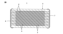
- FIG. 1 is a cross-sectional view schematically showing a multilayer ceramic capacitor 1 according to an embodiment of the present invention.
- the multilayer ceramic capacitor 1 includes a multilayer body 2.
- the laminate 2 includes a plurality of stacked dielectric layers 3 made of ceramic, and a plurality of internal electrodes 4 and 5 arranged along the interface between the plurality of dielectric layers 3.
- the internal electrodes 4 and 5 are classified into a plurality of first internal electrodes 4 and a plurality of second internal electrodes 5, which are alternately arranged in the stacking direction of the laminate 3.
- a first external electrode 6 and a second external electrode 7 are provided on the outer surface of the laminate 2, more specifically, on each opposing end surface.
- the first external electrode 6 is electrically connected to the first internal electrode 4
- the second external electrode 7 is electrically connected to the second internal electrode 5 .
- the dielectric layer 3 is made of, for example, a ceramic whose main component is ABO 3 (A is at least one of Ba, Ca, and Sr, and B is at least one of Ti and Zr). Become. Further, the ceramic may have the above-mentioned ABO 3 as a main component, and may further contain at least one of Mn, Mg, Si, Y, Dy, and Gd as a subcomponent.
- Internal electrodes 4 and 5 contain silver as a conductive component. Furthermore, as a characteristic composition, the internal electrodes 4 and 5 contain at least one selected from AgTiO 3 , EuTiO 3 and NaTiO 3 . AgTiO 3 , EuTiO 3 and NaTiO 3 have an illuminite crystal structure.
- the dielectric layer 3 is made of a ceramic whose main component is at least one selected from BaTiO 3 , SrTiO 3 and CaZrO 3 , and the internal electrodes 4 and 5 contains silver as a conductive component, contains at least one selected from AgTiO 3 , EuTiO 3 and NaTiO 3 as a ceramic material, and optionally contains BaTiO 3 , SrTiO 3 and CaZrO contained in the dielectric layer 3. It further contains at least one species selected from 3 .
- the external electrodes 6 and 7 are formed, for example, by applying a conductive paste containing Ag or Cu as a main conductive component to the end surface of the laminate 2 and baking it. If necessary, for example, Ni plating and Sn plating may be applied on the thick film formed by baking.
- the multilayer ceramic capacitor 1 is manufactured, for example, through the following steps. First, a ceramic slurry containing ceramic raw material powder having the composition as described above is prepared. Next, a suitable sheet forming method is applied to the ceramic slurry to form a ceramic green sheet. Next, a conductive paste to become each of the internal electrodes 4 and 5 is applied by printing or the like onto a predetermined ceramic green sheet among the plurality of ceramic green sheets. Next, a plurality of ceramic green sheets are laminated and then pressed together to obtain a green laminate. The green laminate is then fired. In this firing process, the ceramic green sheet becomes the dielectric layer 3. Thereafter, external electrodes 6 and 7 are formed on the end faces of the laminate 3.
- the conductive paste to become the internal electrodes 4 and 5 used in manufacturing the multilayer ceramic capacitor 1 described above is preferably produced as follows.
- the first step is to prepare a ceramic powder slurry containing ceramic powder, an organic solvent, and a dispersant
- the second step is to prepare a metal powder slurry containing a conductive metal powder, an organic solvent, and a dispersant.
- a third step of preparing an organic vehicle containing an organic resin component and an organic solvent is to prepare a fourth step of mixing the ceramic powder slurry, metal powder slurry, and organic vehicle.
- a ceramic powder slurry is prepared by mixing ceramic powder and a dispersant into an organic solvent.
- the ceramic powder used is, for example, at least one selected from AgTiO 3 , EuTiO 3 and NaTiO 3 as ABO trioxides, and in addition to this, BaTiO 3 and SrTiO 3 as co-materials. 3 and at least one selected from CaZrO 3 and CaZrO 3 may be used.
- the conductive metal powder contained in the metal powder slurry produced in the second step described below contains silver, AgTiO 3 , EuTiO 3 and NaTiO 3 as the above-mentioned ABO 3 oxides have a 6-coordination of silver.
- the ceramic powder made of at least one selected from AgTiO 3 , EuTiO 3 and NaTiO 3 as the ABO trioxide
- the ceramic powder has the above-mentioned ABO trioxide as a main component, and may further contain at least one of Mn, Mg, Si, Y, Dy, and Gd as a subcomponent. When such subcomponents are contained, grain growth of ceramic particles is suppressed, and sintering of metal particles may be effectively suppressed.
- an anionic polymer dispersant for example, an anionic polymer dispersant can be used, and as the organic solvent, for example, dihydroterpineol can be used.
- a metal powder slurry is prepared by mixing conductive metal powder and a dispersant into an organic solvent.
- a powder made of silver is used.
- the dispersant and organic solvent used in the second step those similar to those used in the first step can be used.
- an organic vehicle is produced by mixing an organic resin component with an organic solvent.
- the organic resin component for example, ethyl cellulose resin can be used.
- the organic solvent used in the third step can also be the same as that used in the first step.
- the above-described ceramic powder slurry, metal powder slurry, and organic vehicle are mixed.
- a conductive paste to become the internal electrodes 4 and 5 is obtained.
- This conductive paste contains a ceramic powder slurry, and the ceramic powder slurry is a ceramic powder made of at least one selected from AgTiO 3 , EuTiO 3 and NaTiO 3 as an ABO 3 oxide with a specific ionic radius, as described above. Therefore, the internal electrodes 4 and 5 included in the multilayer ceramic capacitor 1 manufactured through the firing process contain at least one selected from AgTiO 3 , EuTiO 3 and NaTiO 3 .
- silver powder was prepared as the conductive metal powder contained in the conductive paste for forming internal electrodes.
- (Experimental example 1) Main component of ceramic constituting dielectric layer: BaTiO 3 1.
- the main component BaCO 3 and TiO 2 powders were weighed, mixed in a ball mill for 72 hours, and then heat treated at a top temperature of 1000°C for 2 hours. A heat-treated powder was obtained.
- MnO, Dy 2 O 3 , MgO, SiO 2 and BaCO 3 powders were prepared as subcomponents, and the subcomponent powders were 100BaTiO 3 +0.5Mn+1.0Dy+1.0Mg+1.0Si+2. The powders were weighed so as to have a composition ratio of 0Ba, and these subcomponent powders were added to the heat-treated powder, mixed for 24 hours in a ball mill, and then dried to obtain a BaTiO 3 ceramic raw material powder.
- the conductive paste for forming internal electrodes contains the "ABO trioxide " powder shown in Table 2 below and the BaTiO 3 ceramic raw material powder for the dielectric layer. It was used as a ceramic powder.
- ABO 3 oxide powders and BaTiO 3 -based ceramic raw material powder were weighed so as to have the "addition ratio" shown in Table 2, and these powders, dihydroterpineol as an organic solvent, and anion as a dispersant were weighed.
- a ceramic powder slurry was prepared by pre-mixing the mixture and the polymer dispersant using a medium-free stirring mill, and then performing a dispersion treatment using a medium-stirring mill (first step).
- silver powder as a conductive metal powder, dihydroterpineol as an organic solvent, and an anionic polymer dispersant as a dispersant were dispersed in a three-roll mill to prepare a metal powder slurry (second process).
- the metal powder slurry and the ceramic powder slurry were added to the organic vehicle and mixed and dispersed to produce a conductive paste for forming internal electrodes (fourth step).
- Table 2 shows the ratio of the 6-coordinate ionic radius of the A-site element to the 6-coordinate ionic radius of silver to be included in the internal electrode, i.e., "ionic radius ratio (A-site element/metallic silver)". "It is shown. For sample 8, the ratio of the ionic radius (1.35 ⁇ ) of Ba element in the 6-coordination shown in Table 1 to the ionic radius (1.15 ⁇ ) in the 6-coordination of silver is shown. .
- Multilayer Ceramic Capacitor A ceramic slurry containing the BaTiO 3 ceramic raw material powder prepared in 1 above was prepared, and then a doctor blade method was applied to the ceramic slurry to form a ceramic green sheet. Next, the conductive paste for forming internal electrodes prepared in 2 above was applied onto a predetermined ceramic green sheet among the plurality of ceramic green sheets by screen printing. Next, a plurality of ceramic green sheets were laminated and pressed together to obtain a green laminate. The green laminate was then fired. Thereafter, external electrodes were formed on the end faces of the sintered laminate to produce a multilayer ceramic capacitor as a sample.
- the internal electrode and dielectric layer located at the center in the height direction of the laminate provided in the multilayer ceramic capacitor serving as a sample were peeled off from each other by electric field peeling.
- the vicinity of the exposed central part of the internal electrode was observed using a microscope at a magnification of 100 times. Then, by analyzing the obtained images, the ratio of the area occupied by the conductive film as the internal electrode in the exposed portion was determined as the "coverage” shown in Table 2. If the “coverage” is 80% or more, it is judged as good, and enter “ ⁇ ” in the “evaluation” column.If the "coverage” is lower than 80%, it is judged as poor, and in the "evaluation” column, write " ⁇ ". ⁇ ” was entered.
- Samples 1 to 3 and 5 to 7 in Table 2 have an “evaluation” of “ ⁇ ”.
- the internal electrode contains one of AgTiO 3 , EuTiO 3 and NaTiO 3 as the ABO 3 oxide. Further, the internal electrode contains silver as a conductive component.
- the ionic radius of silver in six coordinations is 1.15 ⁇ .
- the ionic radius in the 6-coordination of each A-site element of AgTiO 3 , EuTiO 3 and NaTiO 3 as ABO 3 oxides contained in the internal electrodes in Samples 1 to 3 and 5 to 7 is shown in Table 1. , 1.15 ⁇ , 1.17 ⁇ and 1.02 ⁇ , respectively.
- AgTiO 3 , EuTiO 3 and NaTiO 3 as ABO 3 oxides in Samples 1 to 3 and 5 to 7 have an ionic radius in the 6-coordination of the A-site element in ABO 3 that is included in the internal electrode. Since the ionic radius is equal to or close to the six-coordinate ionic radius of silver as a conductive metal, the energy difference with silver in the internal electrode is 0 or small, so it remains without being ejected from the internal electrode part, and the internal It acts to improve the heat resistance of the electrode. As a result, it is estimated that the coverage of Samples 1 to 3 and 5 to 7 was as high as 82% or more.
- the addition ratio of AgTiO 3 , EuTiO 3 and NaTiO 3 is not necessarily 100%, but if it is 10% or more, none of AgTiO 3 , EuTiO 3 and NaTiO 3 is included. The effect of improving coverage was observed compared to the previous case.
- the ratio of the ionic radius of Ba in six coordinations to the ionic radius of silver in six coordinations that is, the "ionic radius ratio” is 1.17. Therefore, the "ion radius ratio” was outside the range of 0.89 or more and 1.02 or less, and the coverage was as low as 75%.
- Example 2 Main component of ceramic constituting dielectric layer: CaZrO 3 1.
- CaZrO 3 -based ceramic raw material constituting the dielectric layer As starting materials, powders of main components CaCO 3 and ZrO 2 and powders of MnO, SiO 2 and MgO as subcomponents were weighed and heated in a ball mill for 72 hours. After mixing, the mixture was heat treated at a top temperature of 1000° C. for 2 hours to obtain a CaZrO 3 ceramic raw material powder.
- the conductive paste for forming internal electrodes contained the "ABO trioxide " powder shown in Table 3 below and the CaZrO 3 -based ceramic raw material powder for the dielectric layer. It was used as a ceramic powder.
- Samples 11 to 13 and 15 to 17 in Table 3 have an “evaluation” of “ ⁇ ”.
- the internal electrodes contained one of AgTiO 3 , EuTiO 3 and NaTiO 3 as the ABO 3 oxide. Further, the internal electrode contains silver as a conductive component.
- the ionic radius of silver in six coordinations is 1.15 ⁇ .
- the ionic radius in the 6-coordination of each A-site element of AgTiO 3 , EuTiO 3 and NaTiO 3 as ABO 3 oxides contained in the internal electrodes in Samples 11 to 13 and 15 to 17 is shown in Table 1. , 1.15 ⁇ , 1.17 ⁇ and 1.02 ⁇ , respectively.
- AgTiO 3 , EuTiO 3 and NaTiO 3 as ABO 3 oxides in Samples 11 to 13 and 15 to 17 have an ionic radius in the 6-coordination of the A-site element in ABO 3 that is included in the internal electrode. Since the ionic radius is equal to or close to the six-coordinate ionic radius of silver as a conductive metal, the energy difference with silver in the internal electrode is 0 or small, so it remains without being ejected from the internal electrode part, and the internal It is presumed that this acts to improve the heat resistance of the electrode, and as a result, the coverage of Samples 11 to 13 and 15 to 17 was as high as 81% or more.
- the addition ratio of AgTiO 3 , EuTiO 3 and NaTiO 3 is not necessarily 100%, but if it is 10% or more, none of AgTiO 3 , EuTiO 3 and NaTiO 3 is included. The effect of improving coverage was observed compared to the previous case.
- SrTiO 3 Main component of ceramic constituting dielectric layer: SrTiO 3 1.
- SrTiO 3 -based ceramic raw material constituting the dielectric layer As starting materials, the main component SrCO 3 and TiO 2 powders and the subcomponent MnO, SiO 2 and MgO powders were weighed and heated in a ball mill for 72 hours. After mixing, the mixture was heat-treated at a top temperature of 1000° C. for 2 hours to obtain SrTiO 3 ceramic raw material powder.
- the conductive paste for forming internal electrodes contained the "ABO trioxide " powder shown in Table 4 below and the SrTiO 3 -based ceramic raw material powder for the dielectric layer. It was used as a ceramic powder.
- Multilayer Ceramic Capacitor A ceramic slurry containing the SrTiO 3 ceramic raw material powder prepared in 1 above was prepared, and then a doctor blade method was applied to the ceramic slurry to form a ceramic green sheet. Thereafter, a multilayer ceramic capacitor serving as a sample was manufactured through the same steps as in Experimental Example 1.
- Samples 21 to 23 and 25 to 27 in Table 4 have an “evaluation” of “ ⁇ ”.
- the internal electrode contains one of AgTiO 3 , EuTiO 3 and NaTiO 3 as the ABO 3 oxide. Further, the internal electrode contains silver as a conductive component.
- the ionic radius of silver in six coordinations is 1.15 ⁇ .
- the ionic radius in the 6-coordination of each A-site element of AgTiO 3 , EuTiO 3 and NaTiO 3 as ABO 3 oxides contained in the internal electrodes in Samples 21 to 23 and 25 to 27 is shown in Table 1. , 1.15 ⁇ , 1.17 ⁇ and 1.02 ⁇ , respectively.
- AgTiO 3 , EuTiO 3 and NaTiO 3 as ABO 3 oxides in Samples 21 to 23 and 25 to 27 have an ionic radius in the 6-coordination of the A-site element in ABO 3 that is included in the internal electrode. Since the ionic radius is equal to or close to the six-coordinate ionic radius of silver as a conductive metal, the energy difference with silver in the internal electrode is 0 or small, so it remains without being ejected from the internal electrode part, and the internal It is presumed that this acts to improve the heat resistance of the electrode, and as a result, the coverage of Samples 21 to 23 and 25 to 27 was as high as 80% or more.
- the addition ratio of AgTiO 3 , EuTiO 3 and NaTiO 3 is not necessarily 100%, but if it is 10% or more, none of AgTiO 3 , EuTiO 3 and NaTiO 3 is included. The effect of improving coverage was observed compared to the previous case.
- sample 28 which was also evaluated as "x"
- SrTiO 3 as a common material was added to the internal electrode.
- Sr which is an element at the A site in ABO 3 of the perovskite structure, has 12 coordinations, but when it is dissolved in the A site of the illuminite structure, it has 6 coordinations, which is the coordination number of the A site of the illuminite structure. It is necessary to compare the ionic radius at the 6-coordinate position, and the ionic radius at the 6-coordinate position of Sr is 1.18 ⁇ , as shown in Table 1.
- the ratio of the ionic radius of Sr in six coordinations to the ionic radius of silver in six coordinations that is, the "ionic radius ratio” is 1.03. Therefore, the "ion radius ratio" was outside the range of 0.89 or more and 1.02 or less, and the coverage was as low as 70%.
- Embodiments of this invention include the following.
- a laminate comprising a plurality of laminated dielectric layers made of ceramic and a plurality of internal electrodes respectively arranged along the plurality of interfaces between the dielectric layers,
- the internal electrode contains silver as a conductive component and at least one selected from AgTiO 3 , EuTiO 3 and NaTiO 3 .
- Multilayer ceramic capacitor Multilayer ceramic capacitor.
- ⁇ 2> The multilayer ceramic capacitor according to ⁇ 1>, wherein the internal electrode has a thickness of 1 ⁇ m or less.
- ⁇ 3> The multilayer ceramic capacitor according to ⁇ 1> or ⁇ 2>, wherein the internal electrode has a coverage of 80% or more.
- the dielectric layer is made of ceramic containing at least one selected from BaTiO 3 , SrTiO 3 and CaZrO 3 as a main component
- the internal electrode is made of ceramic containing at least one selected from BaTiO 3 , SrTiO 3 and CaZrO 3 contained in the dielectric layer.
- the multilayer ceramic capacitor according to any one of ⁇ 1> to ⁇ 3>, further comprising at least one selected type.
Landscapes
- Engineering & Computer Science (AREA)
- Power Engineering (AREA)
- Manufacturing & Machinery (AREA)
- Microelectronics & Electronic Packaging (AREA)
- Chemical & Material Sciences (AREA)
- Ceramic Engineering (AREA)
- Materials Engineering (AREA)
- Inorganic Chemistry (AREA)
- Ceramic Capacitors (AREA)
- Fixed Capacitors And Capacitor Manufacturing Machines (AREA)
Priority Applications (4)
| Application Number | Priority Date | Filing Date | Title |
|---|---|---|---|
| CN202380028712.1A CN118901114A (zh) | 2022-06-26 | 2023-05-11 | 层叠陶瓷电容器 |
| JP2024530346A JP7711846B2 (ja) | 2022-06-26 | 2023-05-11 | 積層セラミックコンデンサ |
| KR1020247032550A KR102884767B1 (ko) | 2022-06-26 | 2023-05-11 | 적층 세라믹 콘덴서 |
| US18/609,020 US12592339B2 (en) | 2022-06-26 | 2024-03-19 | Multilayer ceramic capacitor |
Applications Claiming Priority (2)
| Application Number | Priority Date | Filing Date | Title |
|---|---|---|---|
| JP2022-102291 | 2022-06-26 | ||
| JP2022102291 | 2022-06-26 |
Related Child Applications (1)
| Application Number | Title | Priority Date | Filing Date |
|---|---|---|---|
| US18/609,020 Continuation US12592339B2 (en) | 2022-06-26 | 2024-03-19 | Multilayer ceramic capacitor |
Publications (1)
| Publication Number | Publication Date |
|---|---|
| WO2024004392A1 true WO2024004392A1 (ja) | 2024-01-04 |
Family
ID=89381977
Family Applications (1)
| Application Number | Title | Priority Date | Filing Date |
|---|---|---|---|
| PCT/JP2023/017694 Ceased WO2024004392A1 (ja) | 2022-06-26 | 2023-05-11 | 積層セラミックコンデンサ |
Country Status (5)
| Country | Link |
|---|---|
| US (1) | US12592339B2 (https=) |
| JP (1) | JP7711846B2 (https=) |
| KR (1) | KR102884767B1 (https=) |
| CN (1) | CN118901114A (https=) |
| WO (1) | WO2024004392A1 (https=) |
Citations (4)
| Publication number | Priority date | Publication date | Assignee | Title |
|---|---|---|---|---|
| JPH05304043A (ja) * | 1992-04-27 | 1993-11-16 | Toshiba Corp | 導体形成用貴金属系組成物 |
| JPH0645183A (ja) * | 1992-07-21 | 1994-02-18 | Matsushita Electric Ind Co Ltd | パラジウムペーストおよび積層チップコンデンサの製造方法 |
| JPH07192528A (ja) * | 1993-12-27 | 1995-07-28 | Nec Corp | 導電性ペースト |
| JP2020202245A (ja) * | 2019-06-07 | 2020-12-17 | 太陽誘電株式会社 | セラミック電子部品の製造方法 |
Family Cites Families (5)
| Publication number | Priority date | Publication date | Assignee | Title |
|---|---|---|---|---|
| JP2016031807A (ja) | 2014-07-28 | 2016-03-07 | 住友金属鉱山株式会社 | 導電性ペースト及びその製造方法 |
| JP6437270B2 (ja) | 2014-10-21 | 2018-12-12 | 株式会社クラレ | ビニルアセタール系重合体樹脂組成物並びにそれを用いたフィルム、セラミックグリーンシート及び積層体 |
| JP2017220524A (ja) * | 2016-06-06 | 2017-12-14 | 株式会社村田製作所 | 積層セラミック電子部品 |
| JP6823976B2 (ja) * | 2016-09-06 | 2021-02-03 | 太陽誘電株式会社 | 積層セラミックコンデンサおよびその製造方法 |
| JP6822155B2 (ja) * | 2017-01-12 | 2021-01-27 | 株式会社村田製作所 | 積層セラミックコンデンサおよびその実装構造体 |
-
2023
- 2023-05-11 WO PCT/JP2023/017694 patent/WO2024004392A1/ja not_active Ceased
- 2023-05-11 KR KR1020247032550A patent/KR102884767B1/ko active Active
- 2023-05-11 CN CN202380028712.1A patent/CN118901114A/zh active Pending
- 2023-05-11 JP JP2024530346A patent/JP7711846B2/ja active Active
-
2024
- 2024-03-19 US US18/609,020 patent/US12592339B2/en active Active
Patent Citations (4)
| Publication number | Priority date | Publication date | Assignee | Title |
|---|---|---|---|---|
| JPH05304043A (ja) * | 1992-04-27 | 1993-11-16 | Toshiba Corp | 導体形成用貴金属系組成物 |
| JPH0645183A (ja) * | 1992-07-21 | 1994-02-18 | Matsushita Electric Ind Co Ltd | パラジウムペーストおよび積層チップコンデンサの製造方法 |
| JPH07192528A (ja) * | 1993-12-27 | 1995-07-28 | Nec Corp | 導電性ペースト |
| JP2020202245A (ja) * | 2019-06-07 | 2020-12-17 | 太陽誘電株式会社 | セラミック電子部品の製造方法 |
Also Published As
| Publication number | Publication date |
|---|---|
| CN118901114A (zh) | 2024-11-05 |
| US20240222016A1 (en) | 2024-07-04 |
| JPWO2024004392A1 (https=) | 2024-01-04 |
| US12592339B2 (en) | 2026-03-31 |
| KR102884767B1 (ko) | 2025-11-11 |
| KR20240158934A (ko) | 2024-11-05 |
| JP7711846B2 (ja) | 2025-07-23 |
Similar Documents
| Publication | Publication Date | Title |
|---|---|---|
| US12437919B2 (en) | Multilayer ceramic capacitor | |
| JP2025156280A (ja) | 積層セラミック電子部品および誘電体磁器組成物 | |
| WO2024004392A1 (ja) | 積層セラミックコンデンサ | |
| WO2024004393A1 (ja) | 積層セラミックコンデンサ | |
| JP2024003265A (ja) | 導電性ペースト | |
| WO2024004391A1 (ja) | 導電性ペースト | |
| WO2024004394A1 (ja) | 積層セラミックコンデンサ | |
| JP2024003266A (ja) | 導電性ペースト | |
| JP7597236B2 (ja) | 導電性ペースト | |
| KR102955824B1 (ko) | 적층 세라믹 콘덴서 | |
| WO2024181021A1 (ja) | 積層セラミックコンデンサ |
Legal Events
| Date | Code | Title | Description |
|---|---|---|---|
| 121 | Ep: the epo has been informed by wipo that ep was designated in this application |
Ref document number: 23830844 Country of ref document: EP Kind code of ref document: A1 |
|
| ENP | Entry into the national phase |
Ref document number: 2024530346 Country of ref document: JP Kind code of ref document: A |
|
| WWE | Wipo information: entry into national phase |
Ref document number: 202380028712.1 Country of ref document: CN |
|
| ENP | Entry into the national phase |
Ref document number: 20247032550 Country of ref document: KR Kind code of ref document: A |
|
| NENP | Non-entry into the national phase |
Ref country code: DE |
|
| 122 | Ep: pct application non-entry in european phase |
Ref document number: 23830844 Country of ref document: EP Kind code of ref document: A1 |