WO2023282191A1 - 基板処理方法及び基板処理装置 - Google Patents
基板処理方法及び基板処理装置 Download PDFInfo
- Publication number
- WO2023282191A1 WO2023282191A1 PCT/JP2022/026372 JP2022026372W WO2023282191A1 WO 2023282191 A1 WO2023282191 A1 WO 2023282191A1 JP 2022026372 W JP2022026372 W JP 2022026372W WO 2023282191 A1 WO2023282191 A1 WO 2023282191A1
- Authority
- WO
- WIPO (PCT)
- Prior art keywords
- metal
- gas
- film
- protective film
- precursor
- Prior art date
Links
- 238000012545 processing Methods 0.000 title claims abstract description 144
- 239000000758 substrate Substances 0.000 title claims abstract description 127
- 238000003672 processing method Methods 0.000 title claims abstract description 23
- 229910052751 metal Inorganic materials 0.000 claims abstract description 259
- 239000002184 metal Substances 0.000 claims abstract description 259
- 230000001681 protective effect Effects 0.000 claims abstract description 127
- 239000002243 precursor Substances 0.000 claims abstract description 99
- YCKRFDGAMUMZLT-UHFFFAOYSA-N Fluorine atom Chemical compound [F] YCKRFDGAMUMZLT-UHFFFAOYSA-N 0.000 claims abstract description 38
- 238000005530 etching Methods 0.000 claims abstract description 38
- 239000011737 fluorine Substances 0.000 claims abstract description 38
- 229910052731 fluorine Inorganic materials 0.000 claims abstract description 38
- 239000007789 gas Substances 0.000 claims description 357
- 238000000034 method Methods 0.000 claims description 140
- 239000000463 material Substances 0.000 claims description 82
- 229910052710 silicon Inorganic materials 0.000 claims description 22
- QVGXLLKOCUKJST-UHFFFAOYSA-N atomic oxygen Chemical compound [O] QVGXLLKOCUKJST-UHFFFAOYSA-N 0.000 claims description 21
- 239000001301 oxygen Substances 0.000 claims description 21
- 229910052760 oxygen Inorganic materials 0.000 claims description 21
- XUIMIQQOPSSXEZ-UHFFFAOYSA-N Silicon Chemical compound [Si] XUIMIQQOPSSXEZ-UHFFFAOYSA-N 0.000 claims description 17
- 239000010703 silicon Substances 0.000 claims description 17
- 229910052718 tin Inorganic materials 0.000 claims description 17
- 229910052719 titanium Inorganic materials 0.000 claims description 17
- QJGQUHMNIGDVPM-UHFFFAOYSA-N nitrogen group Chemical group [N] QJGQUHMNIGDVPM-UHFFFAOYSA-N 0.000 claims description 16
- UFHFLCQGNIYNRP-UHFFFAOYSA-N Hydrogen Chemical compound [H][H] UFHFLCQGNIYNRP-UHFFFAOYSA-N 0.000 claims description 14
- OKTJSMMVPCPJKN-UHFFFAOYSA-N Carbon Chemical compound [C] OKTJSMMVPCPJKN-UHFFFAOYSA-N 0.000 claims description 13
- 229910052736 halogen Inorganic materials 0.000 claims description 13
- 150000002367 halogens Chemical class 0.000 claims description 13
- 229910052759 nickel Inorganic materials 0.000 claims description 13
- 150000004696 coordination complex Chemical class 0.000 claims description 12
- 229910052738 indium Inorganic materials 0.000 claims description 12
- 229910052745 lead Inorganic materials 0.000 claims description 12
- 229910052725 zinc Inorganic materials 0.000 claims description 12
- KRHYYFGTRYWZRS-UHFFFAOYSA-N Fluorane Chemical compound F KRHYYFGTRYWZRS-UHFFFAOYSA-N 0.000 claims description 11
- 229910052799 carbon Inorganic materials 0.000 claims description 11
- 229910052733 gallium Inorganic materials 0.000 claims description 11
- 229910052735 hafnium Inorganic materials 0.000 claims description 11
- 239000001257 hydrogen Substances 0.000 claims description 11
- 229910052739 hydrogen Inorganic materials 0.000 claims description 11
- 229910000040 hydrogen fluoride Inorganic materials 0.000 claims description 11
- 229910052726 zirconium Inorganic materials 0.000 claims description 11
- 229910052782 aluminium Inorganic materials 0.000 claims description 10
- 238000002407 reforming Methods 0.000 claims description 10
- YRKCREAYFQTBPV-UHFFFAOYSA-N acetylacetone Chemical compound CC(=O)CC(C)=O YRKCREAYFQTBPV-UHFFFAOYSA-N 0.000 claims description 8
- 229910052796 boron Inorganic materials 0.000 claims description 8
- NBVXSUQYWXRMNV-UHFFFAOYSA-N fluoromethane Chemical compound FC NBVXSUQYWXRMNV-UHFFFAOYSA-N 0.000 claims description 8
- NINIDFKCEFEMDL-UHFFFAOYSA-N Sulfur Chemical compound [S] NINIDFKCEFEMDL-UHFFFAOYSA-N 0.000 claims description 7
- GDTBXPJZTBHREO-UHFFFAOYSA-N bromine Substances BrBr GDTBXPJZTBHREO-UHFFFAOYSA-N 0.000 claims description 7
- 239000000460 chlorine Substances 0.000 claims description 7
- 239000003446 ligand Substances 0.000 claims description 7
- 239000011593 sulfur Substances 0.000 claims description 7
- 229910052717 sulfur Inorganic materials 0.000 claims description 7
- WKBOTKDWSSQWDR-UHFFFAOYSA-N Bromine atom Chemical compound [Br] WKBOTKDWSSQWDR-UHFFFAOYSA-N 0.000 claims description 6
- ZAMOUSCENKQFHK-UHFFFAOYSA-N Chlorine atom Chemical compound [Cl] ZAMOUSCENKQFHK-UHFFFAOYSA-N 0.000 claims description 6
- CUJRVFIICFDLGR-UHFFFAOYSA-N acetylacetonate Chemical compound CC(=O)[CH-]C(C)=O CUJRVFIICFDLGR-UHFFFAOYSA-N 0.000 claims description 6
- 229910052794 bromium Inorganic materials 0.000 claims description 6
- 229910052801 chlorine Inorganic materials 0.000 claims description 6
- 150000004820 halides Chemical class 0.000 claims description 6
- 150000004767 nitrides Chemical class 0.000 claims description 6
- FZHAPNGMFPVSLP-UHFFFAOYSA-N silanamine Chemical compound [SiH3]N FZHAPNGMFPVSLP-UHFFFAOYSA-N 0.000 claims description 6
- 229910052802 copper Inorganic materials 0.000 claims description 5
- 230000007423 decrease Effects 0.000 claims description 5
- 229910052707 ruthenium Inorganic materials 0.000 claims description 5
- 229910052715 tantalum Inorganic materials 0.000 claims description 5
- SHXHPUAKLCCLDV-UHFFFAOYSA-N 1,1,1-trifluoropentane-2,4-dione Chemical compound CC(=O)CC(=O)C(F)(F)F SHXHPUAKLCCLDV-UHFFFAOYSA-N 0.000 claims description 4
- IGRLELOKIQLMHM-UHFFFAOYSA-N 2,2,5-trimethyloctane-3,4-dione Chemical compound CCCC(C)C(=O)C(=O)C(C)(C)C IGRLELOKIQLMHM-UHFFFAOYSA-N 0.000 claims description 4
- 150000004703 alkoxides Chemical class 0.000 claims description 4
- 125000000217 alkyl group Chemical group 0.000 claims description 4
- 229910052793 cadmium Inorganic materials 0.000 claims description 4
- 125000002915 carbonyl group Chemical group [*:2]C([*:1])=O 0.000 claims description 4
- QAMFBRUWYYMMGJ-UHFFFAOYSA-N hexafluoroacetylacetone Chemical compound FC(F)(F)C(=O)CC(=O)C(F)(F)F QAMFBRUWYYMMGJ-UHFFFAOYSA-N 0.000 claims description 4
- 150000004678 hydrides Chemical class 0.000 claims description 4
- 229910052742 iron Inorganic materials 0.000 claims description 4
- 229910052748 manganese Inorganic materials 0.000 claims description 4
- 230000001590 oxidative effect Effects 0.000 claims description 4
- 229910052697 platinum Inorganic materials 0.000 claims description 4
- 229910052721 tungsten Inorganic materials 0.000 claims description 4
- 239000000126 substance Substances 0.000 abstract description 17
- 239000010936 titanium Substances 0.000 description 14
- 238000006243 chemical reaction Methods 0.000 description 13
- 239000010410 layer Substances 0.000 description 12
- PXHVJJICTQNCMI-UHFFFAOYSA-N nickel Substances [Ni] PXHVJJICTQNCMI-UHFFFAOYSA-N 0.000 description 12
- IJGRMHOSHXDMSA-UHFFFAOYSA-N Atomic nitrogen Chemical compound N#N IJGRMHOSHXDMSA-UHFFFAOYSA-N 0.000 description 10
- 238000000231 atomic layer deposition Methods 0.000 description 10
- 239000011133 lead Substances 0.000 description 9
- 239000011701 zinc Substances 0.000 description 9
- UGFAIRIUMAVXCW-UHFFFAOYSA-N Carbon monoxide Chemical compound [O+]#[C-] UGFAIRIUMAVXCW-UHFFFAOYSA-N 0.000 description 7
- 229910002091 carbon monoxide Inorganic materials 0.000 description 7
- 238000010926 purge Methods 0.000 description 7
- QGZKDVFQNNGYKY-UHFFFAOYSA-N Ammonia Chemical compound N QGZKDVFQNNGYKY-UHFFFAOYSA-N 0.000 description 5
- 239000010949 copper Substances 0.000 description 5
- 125000001153 fluoro group Chemical group F* 0.000 description 5
- 229910044991 metal oxide Inorganic materials 0.000 description 5
- 150000004706 metal oxides Chemical class 0.000 description 5
- 150000002739 metals Chemical class 0.000 description 5
- CURLTUGMZLYLDI-UHFFFAOYSA-N Carbon dioxide Chemical compound O=C=O CURLTUGMZLYLDI-UHFFFAOYSA-N 0.000 description 4
- 229910052581 Si3N4 Inorganic materials 0.000 description 4
- VYPSYNLAJGMNEJ-UHFFFAOYSA-N Silicium dioxide Chemical compound O=[Si]=O VYPSYNLAJGMNEJ-UHFFFAOYSA-N 0.000 description 4
- 238000005229 chemical vapour deposition Methods 0.000 description 4
- 229910052757 nitrogen Inorganic materials 0.000 description 4
- HQVNEWCFYHHQES-UHFFFAOYSA-N silicon nitride Chemical compound N12[Si]34N5[Si]62N3[Si]51N64 HQVNEWCFYHHQES-UHFFFAOYSA-N 0.000 description 4
- 229910052814 silicon oxide Inorganic materials 0.000 description 4
- MYMOFIZGZYHOMD-UHFFFAOYSA-N Dioxygen Chemical compound O=O MYMOFIZGZYHOMD-UHFFFAOYSA-N 0.000 description 3
- -1 carboxylic acid halide Chemical class 0.000 description 3
- 238000004891 communication Methods 0.000 description 3
- 239000000470 constituent Substances 0.000 description 3
- 238000000151 deposition Methods 0.000 description 3
- 238000010586 diagram Methods 0.000 description 3
- 229910001882 dioxygen Inorganic materials 0.000 description 3
- 230000006870 function Effects 0.000 description 3
- 238000010438 heat treatment Methods 0.000 description 3
- 229910001512 metal fluoride Inorganic materials 0.000 description 3
- 229910052750 molybdenum Inorganic materials 0.000 description 3
- 238000003860 storage Methods 0.000 description 3
- 230000003746 surface roughness Effects 0.000 description 3
- 238000012546 transfer Methods 0.000 description 3
- IRPGOXJVTQTAAN-UHFFFAOYSA-N 2,2,3,3,3-pentafluoropropanal Chemical compound FC(F)(F)C(F)(F)C=O IRPGOXJVTQTAAN-UHFFFAOYSA-N 0.000 description 2
- KLZUFWVZNOTSEM-UHFFFAOYSA-K Aluminum fluoride Inorganic materials F[Al](F)F KLZUFWVZNOTSEM-UHFFFAOYSA-K 0.000 description 2
- XKRFYHLGVUSROY-UHFFFAOYSA-N Argon Chemical compound [Ar] XKRFYHLGVUSROY-UHFFFAOYSA-N 0.000 description 2
- 101001090150 Equus caballus Sperm histone P2a Proteins 0.000 description 2
- 229910003902 SiCl 4 Inorganic materials 0.000 description 2
- 150000001412 amines Chemical class 0.000 description 2
- 229910003481 amorphous carbon Inorganic materials 0.000 description 2
- IISBACLAFKSPIT-UHFFFAOYSA-N bisphenol A Chemical compound C=1C=C(O)C=CC=1C(C)(C)C1=CC=C(O)C=C1 IISBACLAFKSPIT-UHFFFAOYSA-N 0.000 description 2
- 150000001722 carbon compounds Chemical class 0.000 description 2
- 239000001569 carbon dioxide Substances 0.000 description 2
- 229910002092 carbon dioxide Inorganic materials 0.000 description 2
- 150000001244 carboxylic acid anhydrides Chemical class 0.000 description 2
- 150000001732 carboxylic acid derivatives Chemical class 0.000 description 2
- 239000003610 charcoal Substances 0.000 description 2
- 239000011651 chromium Substances 0.000 description 2
- 230000008021 deposition Effects 0.000 description 2
- 238000009792 diffusion process Methods 0.000 description 2
- 229910001873 dinitrogen Inorganic materials 0.000 description 2
- 229910052732 germanium Inorganic materials 0.000 description 2
- 125000002887 hydroxy group Chemical group [H]O* 0.000 description 2
- 239000011261 inert gas Substances 0.000 description 2
- 239000012948 isocyanate Substances 0.000 description 2
- 150000002513 isocyanates Chemical class 0.000 description 2
- 229910001509 metal bromide Inorganic materials 0.000 description 2
- 229910001510 metal chloride Inorganic materials 0.000 description 2
- 229910001507 metal halide Inorganic materials 0.000 description 2
- 150000005309 metal halides Chemical class 0.000 description 2
- 239000002052 molecular layer Substances 0.000 description 2
- 125000004433 nitrogen atom Chemical group N* 0.000 description 2
- 229910000069 nitrogen hydride Inorganic materials 0.000 description 2
- 239000005416 organic matter Substances 0.000 description 2
- 229920002120 photoresistant polymer Polymers 0.000 description 2
- 230000001105 regulatory effect Effects 0.000 description 2
- 239000002344 surface layer Substances 0.000 description 2
- 150000003568 thioethers Chemical class 0.000 description 2
- UONOETXJSWQNOL-UHFFFAOYSA-N tungsten carbide Chemical compound [W+]#[C-] UONOETXJSWQNOL-UHFFFAOYSA-N 0.000 description 2
- POILWHVDKZOXJZ-ARJAWSKDSA-M (z)-4-oxopent-2-en-2-olate Chemical compound C\C([O-])=C\C(C)=O POILWHVDKZOXJZ-ARJAWSKDSA-M 0.000 description 1
- OQLZINXFSUDMHM-UHFFFAOYSA-N Acetamidine Chemical class CC(N)=N OQLZINXFSUDMHM-UHFFFAOYSA-N 0.000 description 1
- BSYNRYMUTXBXSQ-UHFFFAOYSA-N Aspirin Chemical compound CC(=O)OC1=CC=CC=C1C(O)=O BSYNRYMUTXBXSQ-UHFFFAOYSA-N 0.000 description 1
- ZOXJGFHDIHLPTG-UHFFFAOYSA-N Boron Chemical compound [B] ZOXJGFHDIHLPTG-UHFFFAOYSA-N 0.000 description 1
- VYZAMTAEIAYCRO-UHFFFAOYSA-N Chromium Chemical compound [Cr] VYZAMTAEIAYCRO-UHFFFAOYSA-N 0.000 description 1
- RYGMFSIKBFXOCR-UHFFFAOYSA-N Copper Chemical compound [Cu] RYGMFSIKBFXOCR-UHFFFAOYSA-N 0.000 description 1
- BRLQWZUYTZBJKN-UHFFFAOYSA-N Epichlorohydrin Chemical compound ClCC1CO1 BRLQWZUYTZBJKN-UHFFFAOYSA-N 0.000 description 1
- 101001139126 Homo sapiens Krueppel-like factor 6 Proteins 0.000 description 1
- VEXZGXHMUGYJMC-UHFFFAOYSA-N Hydrochloric acid Chemical compound Cl VEXZGXHMUGYJMC-UHFFFAOYSA-N 0.000 description 1
- CPELXLSAUQHCOX-UHFFFAOYSA-N Hydrogen bromide Chemical compound Br CPELXLSAUQHCOX-UHFFFAOYSA-N 0.000 description 1
- 229910007991 Si-N Inorganic materials 0.000 description 1
- 229910008051 Si-OH Inorganic materials 0.000 description 1
- BQCADISMDOOEFD-UHFFFAOYSA-N Silver Chemical compound [Ag] BQCADISMDOOEFD-UHFFFAOYSA-N 0.000 description 1
- 229910008284 Si—F Inorganic materials 0.000 description 1
- 229910006294 Si—N Inorganic materials 0.000 description 1
- 229910006358 Si—OH Inorganic materials 0.000 description 1
- ATJFFYVFTNAWJD-UHFFFAOYSA-N Tin Chemical compound [Sn] ATJFFYVFTNAWJD-UHFFFAOYSA-N 0.000 description 1
- RTAQQCXQSZGOHL-UHFFFAOYSA-N Titanium Chemical compound [Ti] RTAQQCXQSZGOHL-UHFFFAOYSA-N 0.000 description 1
- 238000007792 addition Methods 0.000 description 1
- 150000001298 alcohols Chemical class 0.000 description 1
- 150000001409 amidines Chemical class 0.000 description 1
- 229910052787 antimony Inorganic materials 0.000 description 1
- WATWJIUSRGPENY-UHFFFAOYSA-N antimony atom Chemical compound [Sb] WATWJIUSRGPENY-UHFFFAOYSA-N 0.000 description 1
- 229910052786 argon Inorganic materials 0.000 description 1
- 229910052789 astatine Inorganic materials 0.000 description 1
- 238000005513 bias potential Methods 0.000 description 1
- XDRPDDZWXGILRT-FDGPNNRMSA-L bis[[(z)-4-oxopent-2-en-2-yl]oxy]tin Chemical compound [Sn+2].C\C([O-])=C\C(C)=O.C\C([O-])=C\C(C)=O XDRPDDZWXGILRT-FDGPNNRMSA-L 0.000 description 1
- 239000012267 brine Substances 0.000 description 1
- 239000013522 chelant Substances 0.000 description 1
- 229910052804 chromium Inorganic materials 0.000 description 1
- 229910017052 cobalt Inorganic materials 0.000 description 1
- 239000010941 cobalt Substances 0.000 description 1
- GUTLYIVDDKVIGB-UHFFFAOYSA-N cobalt atom Chemical compound [Co] GUTLYIVDDKVIGB-UHFFFAOYSA-N 0.000 description 1
- 150000001875 compounds Chemical class 0.000 description 1
- 230000001276 controlling effect Effects 0.000 description 1
- ROORDVPLFPIABK-UHFFFAOYSA-N diphenyl carbonate Chemical compound C=1C=CC=CC=1OC(=O)OC1=CC=CC=C1 ROORDVPLFPIABK-UHFFFAOYSA-N 0.000 description 1
- GNPVGFCGXDBREM-UHFFFAOYSA-N germanium atom Chemical compound [Ge] GNPVGFCGXDBREM-UHFFFAOYSA-N 0.000 description 1
- VBJZVLUMGGDVMO-UHFFFAOYSA-N hafnium atom Chemical compound [Hf] VBJZVLUMGGDVMO-UHFFFAOYSA-N 0.000 description 1
- 239000013529 heat transfer fluid Substances 0.000 description 1
- 125000004435 hydrogen atom Chemical group [H]* 0.000 description 1
- XLYOFNOQVPJJNP-UHFFFAOYSA-M hydroxide Chemical compound [OH-] XLYOFNOQVPJJNP-UHFFFAOYSA-M 0.000 description 1
- 238000011065 in-situ storage Methods 0.000 description 1
- APFVFJFRJDLVQX-UHFFFAOYSA-N indium atom Chemical compound [In] APFVFJFRJDLVQX-UHFFFAOYSA-N 0.000 description 1
- 238000009616 inductively coupled plasma Methods 0.000 description 1
- 150000002484 inorganic compounds Chemical class 0.000 description 1
- 229910010272 inorganic material Inorganic materials 0.000 description 1
- 150000002500 ions Chemical class 0.000 description 1
- 238000012986 modification Methods 0.000 description 1
- 230000004048 modification Effects 0.000 description 1
- 150000002924 oxiranes Chemical class 0.000 description 1
- TWNQGVIAIRXVLR-UHFFFAOYSA-N oxo(oxoalumanyloxy)alumane Chemical compound O=[Al]O[Al]=O TWNQGVIAIRXVLR-UHFFFAOYSA-N 0.000 description 1
- 150000002989 phenols Chemical class 0.000 description 1
- 229910021420 polycrystalline silicon Inorganic materials 0.000 description 1
- 229920005591 polysilicon Polymers 0.000 description 1
- 239000011241 protective layer Substances 0.000 description 1
- 229910052709 silver Inorganic materials 0.000 description 1
- 239000004332 silver Substances 0.000 description 1
- HPALAKNZSZLMCH-UHFFFAOYSA-M sodium;chloride;hydrate Chemical compound O.[Na+].[Cl-] HPALAKNZSZLMCH-UHFFFAOYSA-M 0.000 description 1
- 239000007787 solid Substances 0.000 description 1
- 238000006467 substitution reaction Methods 0.000 description 1
- JBQYATWDVHIOAR-UHFFFAOYSA-N tellanylidenegermanium Chemical compound [Te]=[Ge] JBQYATWDVHIOAR-UHFFFAOYSA-N 0.000 description 1
- 229910052714 tellurium Inorganic materials 0.000 description 1
- PORWMNRCUJJQNO-UHFFFAOYSA-N tellurium atom Chemical compound [Te] PORWMNRCUJJQNO-UHFFFAOYSA-N 0.000 description 1
- LXEXBJXDGVGRAR-UHFFFAOYSA-N trichloro(trichlorosilyl)silane Chemical compound Cl[Si](Cl)(Cl)[Si](Cl)(Cl)Cl LXEXBJXDGVGRAR-UHFFFAOYSA-N 0.000 description 1
Images


Classifications
-
- H—ELECTRICITY
- H01—ELECTRIC ELEMENTS
- H01L—SEMICONDUCTOR DEVICES NOT COVERED BY CLASS H10
- H01L21/00—Processes or apparatus adapted for the manufacture or treatment of semiconductor or solid state devices or of parts thereof
- H01L21/02—Manufacture or treatment of semiconductor devices or of parts thereof
- H01L21/04—Manufacture or treatment of semiconductor devices or of parts thereof the devices having potential barriers, e.g. a PN junction, depletion layer or carrier concentration layer
- H01L21/18—Manufacture or treatment of semiconductor devices or of parts thereof the devices having potential barriers, e.g. a PN junction, depletion layer or carrier concentration layer the devices having semiconductor bodies comprising elements of Group IV of the Periodic Table or AIIIBV compounds with or without impurities, e.g. doping materials
- H01L21/30—Treatment of semiconductor bodies using processes or apparatus not provided for in groups H01L21/20 - H01L21/26
- H01L21/31—Treatment of semiconductor bodies using processes or apparatus not provided for in groups H01L21/20 - H01L21/26 to form insulating layers thereon, e.g. for masking or by using photolithographic techniques; After treatment of these layers; Selection of materials for these layers
- H01L21/3205—Deposition of non-insulating-, e.g. conductive- or resistive-, layers on insulating layers; After-treatment of these layers
- H01L21/321—After treatment
- H01L21/3213—Physical or chemical etching of the layers, e.g. to produce a patterned layer from a pre-deposited extensive layer
- H01L21/32139—Physical or chemical etching of the layers, e.g. to produce a patterned layer from a pre-deposited extensive layer using masks
-
- C—CHEMISTRY; METALLURGY
- C23—COATING METALLIC MATERIAL; COATING MATERIAL WITH METALLIC MATERIAL; CHEMICAL SURFACE TREATMENT; DIFFUSION TREATMENT OF METALLIC MATERIAL; COATING BY VACUUM EVAPORATION, BY SPUTTERING, BY ION IMPLANTATION OR BY CHEMICAL VAPOUR DEPOSITION, IN GENERAL; INHIBITING CORROSION OF METALLIC MATERIAL OR INCRUSTATION IN GENERAL
- C23F—NON-MECHANICAL REMOVAL OF METALLIC MATERIAL FROM SURFACE; INHIBITING CORROSION OF METALLIC MATERIAL OR INCRUSTATION IN GENERAL; MULTI-STEP PROCESSES FOR SURFACE TREATMENT OF METALLIC MATERIAL INVOLVING AT LEAST ONE PROCESS PROVIDED FOR IN CLASS C23 AND AT LEAST ONE PROCESS COVERED BY SUBCLASS C21D OR C22F OR CLASS C25
- C23F1/00—Etching metallic material by chemical means
- C23F1/10—Etching compositions
- C23F1/12—Gaseous compositions
-
- C—CHEMISTRY; METALLURGY
- C23—COATING METALLIC MATERIAL; COATING MATERIAL WITH METALLIC MATERIAL; CHEMICAL SURFACE TREATMENT; DIFFUSION TREATMENT OF METALLIC MATERIAL; COATING BY VACUUM EVAPORATION, BY SPUTTERING, BY ION IMPLANTATION OR BY CHEMICAL VAPOUR DEPOSITION, IN GENERAL; INHIBITING CORROSION OF METALLIC MATERIAL OR INCRUSTATION IN GENERAL
- C23F—NON-MECHANICAL REMOVAL OF METALLIC MATERIAL FROM SURFACE; INHIBITING CORROSION OF METALLIC MATERIAL OR INCRUSTATION IN GENERAL; MULTI-STEP PROCESSES FOR SURFACE TREATMENT OF METALLIC MATERIAL INVOLVING AT LEAST ONE PROCESS PROVIDED FOR IN CLASS C23 AND AT LEAST ONE PROCESS COVERED BY SUBCLASS C21D OR C22F OR CLASS C25
- C23F1/00—Etching metallic material by chemical means
- C23F1/02—Local etching
-
- H—ELECTRICITY
- H01—ELECTRIC ELEMENTS
- H01L—SEMICONDUCTOR DEVICES NOT COVERED BY CLASS H10
- H01L21/00—Processes or apparatus adapted for the manufacture or treatment of semiconductor or solid state devices or of parts thereof
- H01L21/02—Manufacture or treatment of semiconductor devices or of parts thereof
- H01L21/027—Making masks on semiconductor bodies for further photolithographic processing not provided for in group H01L21/18 or H01L21/34
- H01L21/033—Making masks on semiconductor bodies for further photolithographic processing not provided for in group H01L21/18 or H01L21/34 comprising inorganic layers
- H01L21/0334—Making masks on semiconductor bodies for further photolithographic processing not provided for in group H01L21/18 or H01L21/34 comprising inorganic layers characterised by their size, orientation, disposition, behaviour, shape, in horizontal or vertical plane
- H01L21/0337—Making masks on semiconductor bodies for further photolithographic processing not provided for in group H01L21/18 or H01L21/34 comprising inorganic layers characterised by their size, orientation, disposition, behaviour, shape, in horizontal or vertical plane characterised by the process involved to create the mask, e.g. lift-off masks, sidewalls, or to modify the mask, e.g. pre-treatment, post-treatment
-
- H—ELECTRICITY
- H01—ELECTRIC ELEMENTS
- H01L—SEMICONDUCTOR DEVICES NOT COVERED BY CLASS H10
- H01L21/00—Processes or apparatus adapted for the manufacture or treatment of semiconductor or solid state devices or of parts thereof
- H01L21/02—Manufacture or treatment of semiconductor devices or of parts thereof
- H01L21/04—Manufacture or treatment of semiconductor devices or of parts thereof the devices having potential barriers, e.g. a PN junction, depletion layer or carrier concentration layer
- H01L21/18—Manufacture or treatment of semiconductor devices or of parts thereof the devices having potential barriers, e.g. a PN junction, depletion layer or carrier concentration layer the devices having semiconductor bodies comprising elements of Group IV of the Periodic Table or AIIIBV compounds with or without impurities, e.g. doping materials
- H01L21/30—Treatment of semiconductor bodies using processes or apparatus not provided for in groups H01L21/20 - H01L21/26
- H01L21/302—Treatment of semiconductor bodies using processes or apparatus not provided for in groups H01L21/20 - H01L21/26 to change their surface-physical characteristics or shape, e.g. etching, polishing, cutting
- H01L21/306—Chemical or electrical treatment, e.g. electrolytic etching
- H01L21/3065—Plasma etching; Reactive-ion etching
-
- H—ELECTRICITY
- H01—ELECTRIC ELEMENTS
- H01L—SEMICONDUCTOR DEVICES NOT COVERED BY CLASS H10
- H01L21/00—Processes or apparatus adapted for the manufacture or treatment of semiconductor or solid state devices or of parts thereof
- H01L21/02—Manufacture or treatment of semiconductor devices or of parts thereof
- H01L21/04—Manufacture or treatment of semiconductor devices or of parts thereof the devices having potential barriers, e.g. a PN junction, depletion layer or carrier concentration layer
- H01L21/18—Manufacture or treatment of semiconductor devices or of parts thereof the devices having potential barriers, e.g. a PN junction, depletion layer or carrier concentration layer the devices having semiconductor bodies comprising elements of Group IV of the Periodic Table or AIIIBV compounds with or without impurities, e.g. doping materials
- H01L21/30—Treatment of semiconductor bodies using processes or apparatus not provided for in groups H01L21/20 - H01L21/26
- H01L21/31—Treatment of semiconductor bodies using processes or apparatus not provided for in groups H01L21/20 - H01L21/26 to form insulating layers thereon, e.g. for masking or by using photolithographic techniques; After treatment of these layers; Selection of materials for these layers
- H01L21/3105—After-treatment
- H01L21/311—Etching the insulating layers by chemical or physical means
- H01L21/31105—Etching inorganic layers
- H01L21/31111—Etching inorganic layers by chemical means
- H01L21/31116—Etching inorganic layers by chemical means by dry-etching
- H01L21/31122—Etching inorganic layers by chemical means by dry-etching of layers not containing Si, e.g. PZT, Al2O3
-
- H—ELECTRICITY
- H01—ELECTRIC ELEMENTS
- H01L—SEMICONDUCTOR DEVICES NOT COVERED BY CLASS H10
- H01L21/00—Processes or apparatus adapted for the manufacture or treatment of semiconductor or solid state devices or of parts thereof
- H01L21/02—Manufacture or treatment of semiconductor devices or of parts thereof
- H01L21/04—Manufacture or treatment of semiconductor devices or of parts thereof the devices having potential barriers, e.g. a PN junction, depletion layer or carrier concentration layer
- H01L21/18—Manufacture or treatment of semiconductor devices or of parts thereof the devices having potential barriers, e.g. a PN junction, depletion layer or carrier concentration layer the devices having semiconductor bodies comprising elements of Group IV of the Periodic Table or AIIIBV compounds with or without impurities, e.g. doping materials
- H01L21/30—Treatment of semiconductor bodies using processes or apparatus not provided for in groups H01L21/20 - H01L21/26
- H01L21/31—Treatment of semiconductor bodies using processes or apparatus not provided for in groups H01L21/20 - H01L21/26 to form insulating layers thereon, e.g. for masking or by using photolithographic techniques; After treatment of these layers; Selection of materials for these layers
- H01L21/3105—After-treatment
- H01L21/311—Etching the insulating layers by chemical or physical means
- H01L21/31127—Etching organic layers
- H01L21/31133—Etching organic layers by chemical means
- H01L21/31138—Etching organic layers by chemical means by dry-etching
-
- H—ELECTRICITY
- H01—ELECTRIC ELEMENTS
- H01L—SEMICONDUCTOR DEVICES NOT COVERED BY CLASS H10
- H01L21/00—Processes or apparatus adapted for the manufacture or treatment of semiconductor or solid state devices or of parts thereof
- H01L21/02—Manufacture or treatment of semiconductor devices or of parts thereof
- H01L21/04—Manufacture or treatment of semiconductor devices or of parts thereof the devices having potential barriers, e.g. a PN junction, depletion layer or carrier concentration layer
- H01L21/18—Manufacture or treatment of semiconductor devices or of parts thereof the devices having potential barriers, e.g. a PN junction, depletion layer or carrier concentration layer the devices having semiconductor bodies comprising elements of Group IV of the Periodic Table or AIIIBV compounds with or without impurities, e.g. doping materials
- H01L21/30—Treatment of semiconductor bodies using processes or apparatus not provided for in groups H01L21/20 - H01L21/26
- H01L21/31—Treatment of semiconductor bodies using processes or apparatus not provided for in groups H01L21/20 - H01L21/26 to form insulating layers thereon, e.g. for masking or by using photolithographic techniques; After treatment of these layers; Selection of materials for these layers
- H01L21/3205—Deposition of non-insulating-, e.g. conductive- or resistive-, layers on insulating layers; After-treatment of these layers
- H01L21/321—After treatment
- H01L21/3213—Physical or chemical etching of the layers, e.g. to produce a patterned layer from a pre-deposited extensive layer
- H01L21/32133—Physical or chemical etching of the layers, e.g. to produce a patterned layer from a pre-deposited extensive layer by chemical means only
- H01L21/32135—Physical or chemical etching of the layers, e.g. to produce a patterned layer from a pre-deposited extensive layer by chemical means only by vapour etching only
- H01L21/32136—Physical or chemical etching of the layers, e.g. to produce a patterned layer from a pre-deposited extensive layer by chemical means only by vapour etching only using plasmas
Definitions
- Exemplary embodiments of the present disclosure relate to substrate processing methods and substrate processing apparatuses.
- Patent document 1 discloses a method of atomic layer etching (ALE).
- ALE atomic layer etching
- the substrate is exposed to hydrogen fluoride gas to form a fluorinated surface layer on the metal oxide film.
- the substrate is then exposed to a boron-containing gas to remove the fluorinated surface layer from the metal oxide film.
- the present disclosure provides a substrate processing method and substrate processing apparatus capable of selectively etching a metal-containing film with respect to other films.
- a substrate processing method comprises the steps of (a) providing a substrate having a metal-containing film and a mask provided on the metal-containing film; (b) forming a protective film on the mask; and (c). and after (b), etching the metal-containing film, wherein (c) uses (c1) a first process gas containing a fluorine-containing gas to etch the first gas contained in the metal-containing film. forming a second metal-containing material from one metal-containing material; and (c2) removing said second metal-containing material using a second process gas comprising a precursor.
- a substrate processing method and apparatus are provided that can selectively etch metal-containing films with respect to other films.
- FIG. 1 is a schematic diagram of a substrate processing apparatus according to one exemplary embodiment.
- FIG. 2 is a schematic diagram of a substrate processing apparatus according to one exemplary embodiment.
- FIG. 3 is a partially enlarged cross-sectional view of an example substrate.
- FIG. 4 is a flowchart of a substrate processing method according to one exemplary embodiment.
- FIG. 5 is a partially enlarged cross-sectional view of an exemplary substrate in the step of forming a protective film on the mask.
- FIG. 6 is a partially enlarged cross-sectional view of an example substrate in the process of forming a second metal-containing material.
- FIG. 7 is a partially enlarged cross-sectional view of an example substrate in the step of removing the second metal-containing material.
- FIG. 1 is a schematic diagram of a substrate processing apparatus according to one exemplary embodiment.
- FIG. 2 is a schematic diagram of a substrate processing apparatus according to one exemplary embodiment.
- FIG. 3 is a partially enlarged cross-sectional view of
- FIG. 8 is a partially enlarged cross-sectional view of an exemplary substrate in the step of modifying the surface of the protective film.
- FIG. 9 is a flowchart of a substrate processing method according to one exemplary embodiment.
- FIG. 10 is a flowchart of a substrate processing method according to one exemplary embodiment.
- FIG. 11 is a partially enlarged cross-sectional view of an example substrate.
- FIG. 12 is a partially enlarged cross-sectional view of an exemplary substrate in the step of forming a metal-containing protective film on the mask.
- FIG. 13 is a partially enlarged cross-sectional view of an example substrate in the step of forming a second metal-containing material.
- FIG. 14 is a partially enlarged cross-sectional view of an example substrate in the step of removing the second metal-containing material.
- a substrate processing method includes the steps of: (a) providing a substrate having a metal-containing film and a mask provided over the metal-containing film; and (b) forming a protective film over the mask. and (c) etching the metal-containing film after (b), wherein (c) is (c1) using a first process gas comprising a fluorine-containing gas. forming a second metal-containing material from the first metal-containing material contained in the metal-containing film; and (c2) removing the second metal-containing material using a second process gas containing a precursor. ,including.
- etching of the mask is suppressed by the protective film when etching the metal-containing film. Therefore, the metal-containing film can be selectively etched with respect to other films.
- the substrate processing method may further include (d) the step of removing fluorine from the surface of the protective film using a third processing gas after (c). In this case, a further protective film can be formed in a short time thereafter.
- the substrate processing method may further include (e) the step of repeating (b), (c) and (d) after (d).
- the etching depth of the metal-containing film can be increased.
- the thickness of the protective film formed on the side surface of the mask may decrease from the upper surface of the mask toward the metal-containing film. In this case, since the thickness of the protective film formed on the metal-containing film is reduced, the etching speed of the metal-containing film is improved.
- a plasma generated from the third processing gas may be used in (d) above, and the third processing gas may include at least one of an oxygen-containing gas, a hydrogen-containing gas, and a nitrogen-containing gas.
- the protective film may contain at least one of silicon, carbon and metal.
- the first processing gas may be used without generating plasma.
- plasma generated from the first processing gas may be used.
- the substrate may be heated.
- the reaction between the first metal-containing substance and the fluorine-containing gas or the reaction between the second metal-containing substance and the precursor is promoted.
- the precursor may contain a metal-containing precursor.
- the metal-containing precursor can react with the second metal-containing material at low energy.
- the metal-containing precursor may contain a metal complex.
- a ligand exchange reaction between the second metal-containing substance and the metal complex produces another highly volatile metal complex.
- the metal complex is a complex having at least one monodentate ligand selected from the group consisting of alkyl, hydride, carbonyl, halide, alkoxide, alkylamide and silylamide, or ⁇ -diketonate, amidinate, acetamidinate , ⁇ -diketiminates, diaminoalkoxides and metallocenes.
- the metal contained in the metal-containing precursor may be at least one selected from the group consisting of Sn, Ge, Al, B, Ga, In, Zn, Ni, Pb, Si, Hf, Zr and Ti. .
- the precursor may contain a metal-free precursor.
- metal residue is less likely to occur due to the reaction between the second metal-containing substance and the precursor.
- the metal-free precursor is at least one ⁇ -diketone selected from the group consisting of acac (acetylacetone), hfac (hexafluoroacetylacetone), tfac (trifluoroacetylacetone) and tmhd (tetramethylheptanedione), good too.
- acac acetylacetone
- hfac hexafluoroacetylacetone
- tfac trifluoroacetylacetone
- tmhd tetramethylheptanedione
- the metal-containing film includes Al, Hf, Zr, Fe, Ni, Co, Mn, Mg, Rh, Ru, Cr, Si, Ti, Ga, In, Zn, Pb, Ge, Ta, Cu, W, Mo, It may contain at least one metal selected from the group consisting of Pt, Cd and Sn.
- the metal-containing film may be an oxide or nitride of the metal.
- the fluorine-containing gas may include at least one selected from the group consisting of hydrogen fluoride gas, fluorocarbon gas, nitrogen-containing gas and sulfur-containing gas.
- a substrate processing method includes the steps of: (a) providing a substrate having a film to be etched and a mask provided over the film to be etched; forming a protective film; (c) removing a portion of the metal-containing protective film after (b); and (d) etching the etching target film after (c).
- (b) includes (b1) forming a precursor layer on the side surface of the mask using a first precursor containing a metal; and (c) reforming the precursor layer into the metal-containing protective film using a gaseous gas, wherein (c1) a first gas containing at least one of a halogen-containing gas and an oxygen-containing gas; forming a second metal-containing material from a first metal-containing material contained in the metal-containing protective film using a process gas; and (c2) using a second process gas containing a second precursor to form the second metal-containing material. and removing the metal-containing material.
- the metal-containing protective film can be etched at a high selectivity with respect to the film to be etched and the mask.
- the first precursor may contain at least one metal selected from the group consisting of Ti, Ta, Ru, Al, Hf and Sn.
- the halogen-containing gas may contain at least one selected from the group consisting of fluorine, chlorine and bromine.
- the second precursor is a metal containing at least one selected from the group consisting of Sn, Ge, Al, B, Ga, In, Zn, Ni, Pb, Si, Hf, Zr and Ti, or a complex of the metal. may contain.
- the film to be etched may be a silicon-containing film.
- the substrate processing apparatus includes a chamber and a substrate support for supporting a substrate in the chamber, the substrate comprising a metal-containing film and a metal-containing film provided on the metal-containing film.
- a substrate support having a mask; a first process gas including hydrogen fluoride gas; a second process gas including a precursor; a third process gas; and a fourth process gas for forming a protective film.
- a gas supply section each configured to supply into the chamber; and a control section, wherein the control section controls the gas supply to form the protective film on the mask using the fourth process gas.
- the gas supply unit is configured to control the gas supply unit so as to
- etching of the mask is suppressed by the protective film when etching the metal-containing film. Therefore, the metal-containing film can be selectively etched with respect to other films. Furthermore, the third process gas is used to remove fluorine from the surface of the protective film. Therefore, a further protective film can be formed in a short time thereafter.
- FIG. 1 and 2 are diagrams schematically showing a substrate processing apparatus according to one exemplary embodiment.
- the substrate processing apparatus of this embodiment is, for example, a plasma processing system.
- the plasma processing system includes a plasma processing apparatus 1 and a controller 2.
- the plasma processing apparatus 1 includes a plasma processing chamber 10 , a substrate support section 11 and a plasma generation section 12 .
- Plasma processing chamber 10 has a plasma processing space.
- the plasma processing chamber 10 also has at least one gas inlet for supplying at least one process gas to the plasma processing space and at least one gas outlet for exhausting gas from the plasma processing space.
- the gas supply port is connected to a gas supply section 20, which will be described later, and the gas discharge port is connected to an exhaust system 40, which will be described later.
- the substrate support 11 is arranged in the plasma processing space and has a substrate support surface for supporting the substrate.
- the plasma generation unit 12 is configured to generate plasma from at least one processing gas supplied into the plasma processing space.
- the plasma formed in the plasma processing space includes capacitively coupled plasma (CCP), inductively coupled plasma (ICP), ECR plasma (Electron-Cyclotron-resonance plasma), helicon wave excited plasma (HWP). Wave Plasma), surface wave plasma (SWP: Surface Wave Plasma), or the like.
- Various types of plasma generators may also be used, including AC (Alternating Current) plasma generators and DC (Direct Current) plasma generators.
- the AC signal (AC power) used in the AC plasma generator has a frequency within the range of 100 kHz to 10 GHz.
- AC signals include RF (Radio Frequency) signals and microwave signals.
- the RF signal has a frequency within the range of 200 kHz-150 MHz.
- the controller 2 processes computer-executable instructions that cause the plasma processing apparatus 1 to perform the various steps described in this disclosure. Controller 2 may be configured to control elements of plasma processing apparatus 1 to perform the various processes described herein. In one embodiment, part or all of the controller 2 may be included in the plasma processing apparatus 1 .
- the control unit 2 may include, for example, a computer 2a.
- the computer 2a may include, for example, a processing unit (CPU: Central Processing Unit) 2a1, a storage unit 2a2, and a communication interface 2a3. Processing unit 2a1 can be configured to perform various control operations based on programs stored in storage unit 2a2.
- the storage unit 2a2 may include RAM (Random Access Memory), ROM (Read Only Memory), HDD (Hard Disk Drive), SSD (Solid State Drive), or a combination thereof.
- the communication interface 2a3 may communicate with the plasma processing apparatus 1 via a communication line such as a LAN (Local Area Network).
- the plasma processing system includes a capacitively-coupled plasma processing apparatus 1 and a controller 2 .
- the capacitively coupled plasma processing apparatus 1 includes a plasma processing chamber 10, a gas supply section 20, a power supply 30 and an exhaust system 40.
- the plasma processing apparatus 1 includes a substrate support section 11 and a gas introduction section.
- the gas introduction is configured to introduce at least one process gas into the plasma processing chamber 10 .
- the gas introduction section includes a showerhead 13 .
- a substrate support 11 is positioned within the plasma processing chamber 10 .
- the showerhead 13 is arranged above the substrate support 11 . In one embodiment, showerhead 13 forms at least a portion of the ceiling of plasma processing chamber 10 .
- the plasma processing chamber 10 has a plasma processing space 10 s defined by a showerhead 13 , side walls 10 a of the plasma processing chamber 10 and a substrate support 11 .
- the plasma processing chamber 10 has at least one gas supply port for supplying at least one processing gas to the plasma processing space 10s and at least one gas exhaust port for exhausting gas from the plasma processing space.
- Side wall 10a is grounded.
- the showerhead 13 and substrate support 11 are electrically insulated from the plasma processing chamber 10 housing.
- the substrate support section 11 includes a body section 111 and a ring assembly 112 .
- the body portion 111 has a central region (substrate support surface) 111 a for supporting the substrate (wafer) W and an annular region (ring support surface) 111 b for supporting the ring assembly 112 .
- the annular region 111b of the body portion 111 surrounds the central region 111a of the body portion 111 in plan view.
- the substrate W is arranged on the central region 111 a of the main body 111
- the ring assembly 112 is arranged on the annular region 111 b of the main body 111 so as to surround the substrate W on the central region 111 a of the main body 111 .
- body portion 111 includes a base and an electrostatic chuck.
- the base includes an electrically conductive member.
- the conductive member of the base functions as a lower electrode.
- An electrostatic chuck is arranged on the base.
- the upper surface of the electrostatic chuck has a substrate support surface 111a.
- Ring assembly 112 includes one or more annular members. At least one of the one or more annular members is an edge ring.
- the substrate supporter 11 may include a temperature control module configured to control at least one of the electrostatic chuck, the ring assembly 112, and the substrate to a target temperature.
- the temperature control module may include heaters, heat transfer media, flow paths, or combinations thereof.
- a heat transfer fluid, such as brine or gas flows through the channel.
- the substrate support section 11 may include a heat transfer gas supply section configured to supply a heat transfer gas between the back surface of the substrate W and the substrate support surface 111a.
- the showerhead 13 is configured to introduce at least one processing gas from the gas supply unit 20 into the plasma processing space 10s.
- the showerhead 13 has at least one gas supply port 13a, at least one gas diffusion chamber 13b, and multiple gas introduction ports 13c.
- the processing gas supplied to the gas supply port 13a passes through the gas diffusion chamber 13b and is introduced into the plasma processing space 10s through a plurality of gas introduction ports 13c.
- showerhead 13 also includes a conductive member.
- a conductive member of the showerhead 13 functions as an upper electrode.
- the gas introduction part may include one or more side gas injectors (SGI: Side Gas Injector) attached to one or more openings formed in the side wall 10a.
- SGI Side Gas Injector
- the gas supply unit 20 may include at least one gas source 21 and at least one flow controller 22 .
- gas supply 20 is configured to supply at least one process gas from respective gas sources 21 through respective flow controllers 22 to showerhead 13 .
- Each flow controller 22 may include, for example, a mass flow controller or a pressure controlled flow controller.
- gas supply 20 may include one or more flow modulation devices that modulate or pulse the flow of at least one process gas.
- Power supply 30 includes an RF power supply 31 coupled to plasma processing chamber 10 via at least one impedance matching circuit.
- RF power supply 31 is configured to supply at least one RF signal (RF power), such as a source RF signal and a bias RF signal, to conductive members of substrate support 11 and/or conductive members of showerhead 13 . be done.
- RF power source 31 may function as at least part of a plasma generator configured to generate a plasma from one or more process gases in plasma processing chamber 10 .
- a bias potential is generated in the substrate W, and ion components in the formed plasma can be drawn into the substrate W.
- the RF power supply 31 includes a first RF generator 31a and a second RF generator 31b.
- the first RF generator 31a is coupled to the conductive member of the substrate support 11 and/or the conductive member of the showerhead 13 via at least one impedance matching circuit to provide a source RF signal for plasma generation (source RF electrical power).
- the source RF signal has a frequency within the range of 13 MHz to 150 MHz.
- the first RF generator 31a may be configured to generate multiple source RF signals having different frequencies. The generated one or more source RF signals are provided to conductive members of the substrate support 11 and/or conductive members of the showerhead 13 .
- the second RF generator 31b is coupled to the conductive member of the substrate support 11 via at least one impedance matching circuit and configured to generate a bias RF signal (bias RF power).
- the bias RF signal has a lower frequency than the source RF signal.
- the bias RF signal has a frequency within the range of 400 kHz to 13.56 MHz.
- the second RF generator 31b may be configured to generate multiple bias RF signals having different frequencies.
- One or more bias RF signals generated are provided to the conductive members of the substrate support 11 .
- at least one of the source RF signal and the bias RF signal may be pulsed.
- Power supply 30 may also include a DC power supply 32 coupled to plasma processing chamber 10 .
- the DC power supply 32 includes a first DC generator 32a and a second DC generator 32b.
- the first DC generator 32a is connected to a conductive member of the substrate support 11 and configured to generate the first DC signal.
- the generated first bias DC signal is applied to the conductive members of substrate support 11 .
- the first DC signal may be applied to other electrodes, such as electrodes in an electrostatic chuck.
- the second DC generator 32b is connected to the conductive member of the showerhead 13 and configured to generate the second DC signal.
- the generated second DC signal is applied to the conductive members of showerhead 13 .
- at least one of the first and second DC signals may be pulsed. Note that the first and second DC generators 32a and 32b may be provided in addition to the RF power supply 31, and the first DC generator 32a may be provided instead of the second RF generator 31b. good.
- the exhaust system 40 may be connected to a gas exhaust port 10e provided at the bottom of the plasma processing chamber 10, for example.
- Exhaust system 40 may include a pressure regulating valve and a vacuum pump.
- the pressure regulating valve regulates the pressure in the plasma processing space 10s.
- Vacuum pumps may include turbomolecular pumps, dry pumps, or combinations thereof.
- FIG. 3 is a partially enlarged cross-sectional view of an example substrate.
- the substrate W comprises a metal-containing film MF and a mask MK.
- a mask MK is provided on the metal-containing film MF.
- the substrate W may comprise an underlying region UR.
- the underlying region UR may contain silicon.
- the metal-containing film MF can be provided on the base region UR.
- the metal-containing film MF may contain at least one of oxygen and nitrogen.
- the metal-containing film MF may include at least one of metal oxide and metal nitride.
- the metal-containing film MF is Al, Hf, Zr, Fe, Ni, Co, Mn, Mg, Rh, Ru, Cr, Si, Ti, Ga, In, Zn, Pb, Ge, Ta, Cu, W, Mo, At least one of Pt, Cd and Sn may be included.
- the mask MK may contain silicon.
- the mask MK may include at least one of silicon oxide and silicon nitride.
- the mask MK may contain carbon (organic matter).
- Mask MK may include at least one of photoresist, spin-on carbon, amorphous carbon, and tungsten carbide.
- the mask MK may have at least one recess RS. Each recess RS may be an opening.
- FIG. 4 is a flowchart of a substrate processing method according to one exemplary embodiment.
- the substrate processing method shown in FIG. 4 (hereinafter referred to as "method MT1") can be performed by the substrate processing apparatus of the above embodiment.
- Method MT1 may include steps ST1 to ST5. Steps ST1 to ST5 may be performed in order. Process ST5 may not be performed.
- the method MT1 will be described below with reference to FIGS. 4 to 8.
- FIG. When the plasma processing apparatus 1 is used, the method MT1 can be executed in the plasma processing apparatus 1 by controlling each section of the plasma processing apparatus 1 by the control unit 2 .
- the metal-containing film MF can be etched.
- Steps ST1 to ST5 may be performed in-situ. That is, the method MT1 may be performed without taking the substrate W out of the plasma processing chamber 10 .
- step ST1 a substrate W shown in FIG. 3 is provided.
- a substrate W may be supported within the plasma processing chamber 10 by a substrate support 11, as shown in FIG.
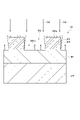
- FIG. 5 is a partially enlarged cross-sectional view of an exemplary substrate in the step of forming a protective film on the mask.
- a protective film PR is formed on the mask MK.
- the protective film PR can be formed by atomic layer deposition (ALD), molecular layer deposition (MLD) or chemical vapor deposition (CVD).
- a fourth process gas may be used to form the protective film PR.
- a fourth processing gas is supplied into the plasma processing chamber 10 from the gas supply section 20 . Within the plasma processing chamber 10, the substrate W is exposed to a fourth processing gas.
- a precursor gas and a modifying gas are used as the fourth processing gas.
- the protective film PR can be formed on the upper surface MKt and side surfaces MKs of the mask MK.
- the thickness of the protective film PR formed over the upper surface MKt of the mask MK is greater than the thickness of the protective film PR formed over the side surfaces MKs of the mask MK.
- the thickness of the protective film PR formed on the side surface MKs of the mask MK may decrease from the upper surface MKt of the mask MK toward the metal-containing film MF. That is, the protective film PR may be a subconformal film.
- the protective film PR may not be formed on the metal-containing film MF at the bottom of the recess RS of the mask MK.
- the thickness of the protective film PR formed on the bottom of the recess RS of the mask MK is smaller than the thickness of the protective film PR formed on the upper surface MKt and side surfaces MKs of the mask MK.
- the protective film PR may be a conformal film.
- the protective film PR formed on the bottom of the recess RS of the mask MK can be selectively removed by, for example, anisotropic etching.
- the protective film PR can be left on the upper surface MKt and the side surfaces MKs of the mask MK, while the protective film PR at the bottom of the concave portion RS of the mask MK can be removed.
- the protective film PR may contain at least one of silicon, carbon and metal.
- the protective film PR has a silicon oxide film formed by ALD or MLD
- a silicon-containing gas such as aminosilane, SiCl 4 or SiF 4 is used as the precursor gas, and an oxygen-containing gas such as oxygen gas is used as the modifying gas.
- an oxygen-containing gas such as oxygen gas
- the protective film PR has a silicon nitride film formed by ALD or MLD
- a silicon-containing gas such as aminosilane, SiCl 4 , gchlorosilane, hexachlorodisilane, or the like can be used as the precursor gas.
- a nitrogen-containing gas such as ammonia gas or nitrogen gas can be used as the reforming gas.
- the protective film PR has an organic film formed by ALD
- epoxide, carboxylic acid, carboxylic acid halide, carboxylic anhydride, isocyanate, phenols, or the like can be used as the precursor gas.
- An inorganic compound gas having an NH bond, an inert gas, a mixed gas of N 2 and H 2 , a H 2 O gas, a mixed gas of H 2 and O 2 , or the like can be used as the reforming gas.
- an isocyanate, a carboxylic acid, or a carboxylic acid halide can be used as the precursor gas, and an amine or a compound having a hydroxyl group can be used as the modifying gas.
- a carboxylic anhydride can be used as the precursor gas and an amine as the reforming gas.
- bisphenol A can be used as the precursor gas and diphenyl carbonate or epichlorohydrin as the reforming gas.
- the protective film PR has a metal-containing film formed by ALD or MLD
- gases containing metals such as Ti, Ta, Ru, Al, Hf or Sn as precursor gases, or oxides of these metals
- Metal-containing gases such as gases containing nitrides, sulfides or halides may be used.
- Hydrogen-containing gas (H2, etc.), oxygen - containing gas ( O2 , etc.), mixed gas of H2 and N2 , gas containing hydrogen and nitrogen ( NH3 , etc.), etc. gas can be used.
- a step ST12 of removing the protective film PR formed on the bottom of the recess RS of the mask MK may be performed.
- Process ST12 may be performed before process ST3.
- the protective film PR is a silicon-containing film
- the protective film PR formed at the bottom of the recess RS can be removed in step ST12 by plasma generated from a fluorine-containing gas.
- the protective film PR is an organic film
- the protective film PR formed on the bottom of the recess RS can be removed with O 2 gas or H 2 gas.
- Process ST3 In step ST3, the metal containing film MF is etched.
- the metal-containing film MF may be etched by atomic layer etching (ALE).
- Process ST3 includes process ST31 and process ST32.
- Process ST32 is performed after process ST31.
- step ST31 and step ST32 may be alternately repeated.
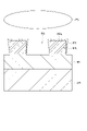
- FIG. 6 is a partially enlarged cross-sectional view of an example substrate in the process of forming a second metal-containing material.
- the first processing gas G1 containing fluorine-containing gas is used to form the second metal-containing material MS2 from the first metal-containing material MS1 (see FIG. 5) contained in the metal-containing film MF.
- the first metal-containing material MS1 may be located on the surface of the metal-containing film MF.
- the protective film PR on the mask MK is thinned and the protective film PR on the metal-containing film MF is removed. Thereby, the surface of the metal-containing film MF is exposed to the first processing gas G1.
- the first metal-containing material MS1 reacts with the first process gas G1.
- the first processing gas G1 is supplied into the plasma processing chamber 10 from the gas supply section 20 . Within the plasma processing chamber 10, the substrate W is exposed to a first processing gas G1.
- the fluorine-containing gas may include at least one of hydrogen fluoride gas (HF gas), fluorocarbon gas, nitrogen-containing gas, and sulfur-containing gas.
- the fluorocarbon gas can include at least one of C4F6 gas, C4F8 gas , C3F8 gas, and CF4 gas.
- the nitrogen - containing gas can include NF3 gas.
- Sulfur-containing gas may include SF6 gas.
- the first metal-containing substance MS1 is the same as an example of the constituent material of the metal-containing film MF.
- the second metal-containing material MS2 can be produced from a reaction between the first metal-containing material MS1 and a fluorine-containing gas.
- the second metal-containing material MS2 may contain the same metal as the metal contained in the first metal-containing material MS1 and fluorine.
- the second metal-containing substance MS2 is, for example, a metal fluoride.
- the first metal-containing material MS1 comprises aluminum oxide and the fluorine-containing gas comprises hydrogen fluoride gas.
- the second metal-containing material MS2 comprises aluminum fluoride.
- the surface PRs of the protective film PR may be fluorinated by the reaction between the surface PRs of the protective film PR and the fluorine-containing gas. As a result, fluorine may remain on the surface PRs of the protective film PR.
- the first processing gas G1 may be used without generating plasma, or plasma generated from the first processing gas G1 may be used.
- the first processing gas G1 may contain hydrogen fluoride gas.
- the substrate W may be heated in step ST31.
- the temperature of the substrate support 11 may be 100° C. or higher, 150° C. or higher, or 200° C. or higher.
- the temperature of the substrate support 11 may be 450° C. or less.
- Heating may be provided by a plasma generated within the plasma processing chamber 10 or by a temperature control module within the substrate support 11 . The heating promotes the reaction between the first metal-containing material MS1 and the fluorine-containing gas.
- a purge step may be performed after step ST31.
- the purge gas is supplied into the plasma processing chamber 10, the purge gas is exhausted.
- the purge gas is an inert gas such as nitrogen or argon.
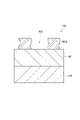
- FIG. 7 is a partially enlarged cross-sectional view of an example substrate in the step of removing the second metal-containing material.
- the second metal-containing material MS2 is removed using the second processing gas G2 containing the precursor.
- the second processing gas G2 is supplied from the gas supply section 20 into the plasma processing chamber 10 .
- the second processing gas G2 can be used without generating plasma.
- the substrate W is exposed to a second processing gas G2.
- the precursor may include a metal-containing precursor.
- Metal-containing precursors may include metal complexes.
- the metal complex may be a complex with a monodentate ligand or a chelate.
- the monodentate ligand can be at least one of alkyl, hydride, carbonyl, halide, alkoxide, alkylamide and silylamide.
- Chelates can be at least one of ⁇ -diketonates, amidinates, acetamidinates, ⁇ -diketiminates, diaminoalkoxides and metallocenes.
- the ⁇ -diketonate can be at least one of acac (acetylacetonate), hfac (hexafluoroacetylacetonate), tfac (trifluoroacetylacetonate) and tmhd (tetramethylheptanedionate).
- the metal contained in the metal-containing precursor may be at least one of Sn, Ge, Al, B, Ga, In, Zn, Ni, Pb, Si, Hf, Zr and Ti.
- the precursor may include a metal-free precursor.
- Metal-free precursors may include carbon-containing precursors.
- Carbon-containing precursors can be at least one of alcohols, ⁇ -diketones, amidines, acetamidines and ⁇ -diketimines.
- the ⁇ -diketone can be at least one of acac (acetylacetone), hfac (hexafluoroacetylacetone), tfac (trifluoroacetylacetone) and tmhd (tetramethylheptanedione).
- the reaction between the second metal-containing substance MS2 and the precursor can produce a volatile third metal-containing substance MS3.
- the precursor includes a metal-containing precursor
- the metal-containing precursor can react with the second metal-containing material at low energy.
- the metal-containing precursor contains a metal complex
- the ligand exchange reaction between the second metal-containing substance MS2 and the metal complex produces another highly volatile metal complex.
- the second metal-containing material MS2 comprises aluminum fluoride and the metal-containing precursor comprises tin(II) acetylacetonate (Sn(acac) 2 ).
- the precursor contains a precursor that does not contain metal
- metal residue is less likely to occur due to the reaction between the second metal-containing substance and the precursor. If the metal-free precursor contains a carbon-containing precursor, a residue containing carbon compounds is produced. Residues containing carbon compounds can be removed relatively easily.
- step ST32 the substrate W may be heated as in step ST31.
- the heating promotes the reaction between the second metal-containing material MS2 and the precursor.
- a purge step may be performed in the same manner as the purge step performed after step ST31.
- FIG. 8 is a partially enlarged cross-sectional view of an exemplary substrate in the step of modifying the surface of the protective film.
- the surface PRs of the protective film PR is modified.
- fluorine is removed from the surface PRs of the protective film PR using the third processing gas.
- the plasma PL generated from the third processing gas is used in step ST4.
- the plasma PL can be generated by the plasma generation unit 12 from the third processing gas supplied from the gas supply unit 20 into the plasma processing chamber 10 .
- substrate W is exposed to plasma PL.
- a third process gas may be used without generating a plasma.
- Si—F bonds may remain on the surface PRs of the protective film PR after step ST31.
- the plasma PL generated from the third processing gas containing the oxygen-containing gas fluorine atoms on the surface PRs of the protective film PR are replaced with OH groups.
- Si—OH bonds are formed on the surface PRs of the protective film PR.
- fluorine atoms on the surface PRs of the protective film PR are replaced with hydrogen atoms.
- Si—H bonds are formed on the surface PRs of the protective film PR.
- C—F bonds may exist on the surface PRs of the protective film PR after step ST31.
- fluorine atoms on the surface PRs of the protective film PR are replaced with H groups by using the plasma PL generated from the third processing gas containing the oxygen-containing gas or the hydrogen-containing gas.
- a CH bond is formed on the surface PRs of the protective film PR. This is because the produced carbon monoxide volatilizes.
- fluorine atoms on the surface PRs of the protective film PR are replaced with nitrogen atoms.
- a CN bond is formed on the surface PRs of the protective film PR.
- the surface PRs of the protective film PR is shaved by using the plasma PL generated from the third processing gas containing nitrogen-containing gas.
- the constituent material of the protective film PR is exposed on the surface PRs of the protective film PR.
- the constituent material contains a C—H bond
- the C—H bond is exposed on the surface PRs of the protective film PR.
- steps ST2, ST3 and ST4 are repeated.
- Step ST2, step ST3 and step ST4 may be repeated multiple times.
- the etching depth of the metal-containing film MF can be increased by the step ST5.
- etching of the mask MK is suppressed by the protective film PR when the metal-containing film MF is etched. Therefore, the metal-containing film MF can be selectively etched with respect to other films. Furthermore, the process ST4 removes fluorine from the surface PRs of the protective film PR. If fluorine remains on the surface PRs of the protective film PR, it tends to take a long time to start depositing the protective film PR. In the method MT1, since the fluorine on the surface PRs of the protective film PR is removed in the step ST4, a further protective film PR can be formed thereafter in a short time.
- step ST2 if the thickness of the protective film PR formed on the side surface MKs of the mask MK decreases from the upper surface MKt of the mask MK toward the metal-containing film MF, the protective film PR is formed on the metal-containing film MF.
- the thickness of the protective film PR to be applied is reduced. Therefore, since the protective film PR on the metal-containing film MF can be removed in a short time, the etching speed of the metal-containing film MF is improved.
- the substrate processing apparatus does not have to include the plasma generator 12 .
- plasma processing is not performed in the chamber of the substrate processing apparatus.
- Method MT1 can also be performed using such a substrate processing apparatus.
- the first processing gas G1 may contain a halogen-containing gas.
- the first processing gas G1 may include at least one of a chlorine-containing gas and a bromine-containing gas instead of or together with the fluorine-containing gas described above.
- the chlorine-containing gas may include at least one of chlorine (Cl 2 ) gas and hydrogen chloride (HCl) gas.
- the bromine-containing gas may include at least one of bromine (Br2) gas and hydrogen bromide (HBr) gas.
- the halogen-containing gas may contain at least one of silicon and carbon.
- the second metal-containing material M2 generated in step ST31 can be formed by the reaction between the first metal-containing material MS1 and the halogen-containing gas.
- the second metal-containing material MS2 may contain the same metal as the metal contained in the first metal-containing material MS1, and halogen.
- the second metal-containing material MS2 is, for example, a metal halide.
- the second metal-containing material MS2 can be a metal fluoride, metal chloride or metal bromide. Even when the second metal-containing substance MS2 is a metal halide (metal chloride or metal bromide) other than a metal fluoride, the second metal-containing substance MS2 is the second processing gas G2 containing the above precursor. can be removed by
- the first processing gas G1 may contain an oxygen-containing gas instead of or together with the halogen-containing gas.
- the first processing gas G1 may contain at least one of oxygen (O 2 ) gas, carbon monoxide (CO) gas, and carbon dioxide gas (CO 2 ) as the oxygen-containing gas.
- the second metal-containing material M2 generated in step ST31 can be formed by the reaction between the first metal-containing material MS1 and the oxygen-containing gas.
- the second metal-containing material MS2 may contain the same metal as the metal contained in the first metal-containing material MS1, and oxygen.
- the second metal-containing material MS2 is, for example, a metal oxide. If the second metal-containing material MS2 is a metal oxide, the second metal-containing material MS2 can be removed by a second process gas G2 that includes the metal-free precursors described above.
- FIG. 9 is a flowchart of a substrate processing method according to another embodiment 4.
- FIG. 9 The substrate processing method shown in FIG. 9 (hereinafter referred to as “method MT2”) can include steps ST1 to ST5 like method MT1.
- Method MT2 includes step ST33 after step ST32 and before step ST4.
- Step ST33 is a step of exposing the substrate W to plasma generated from a fifth processing gas containing at least one of fluorine-containing gas, oxygen-containing gas, hydrogen-containing gas, and nitrogen-containing gas.
- the fluorine-containing gas may include at least one of fluorocarbon gas, nitrogen-containing gas and sulfur-containing gas.
- the fluorocarbon gas may include at least one of C4F6 gas, C4F8 gas , C3F8 gas and CF4 gas.
- the nitrogen - containing gas can include NF3 gas.
- Sulfur-containing gas may include SF6 gas.
- the oxygen-containing gas may include at least one of oxygen gas, carbon monoxide gas and carbon dioxide gas.
- the hydrogen containing gas may include hydrogen gas.
- the nitrogen-containing gas may include nitrogen gas.
- the fifth processing gas may contain at least one of hydrogen gas, CH4 gas and carbon monoxide gas.
- the precursor used in step ST32 contains Si, Ge, or B
- the fifth processing gas may contain a fluorine-containing gas.
- the fifth processing gas may contain at least one of CH4 gas and carbon monoxide gas.
- the fifth processing gas may include at least one of hydrogen gas and oxygen gas.
- FIG. 10 is a flowchart of a substrate processing method according to another embodiment 5.
- FIG. 10 The substrate processing method shown in FIG. 10 (hereinafter referred to as “method MT3”) can include steps ST1a to ST5a. Steps ST1a to ST5a may be performed in order. Method MT3 may not include step ST4a.
- Step ST1a the substrate Wa shown in FIG. 11 is provided.
- the substrate Wa includes an etching target film EF and a mask MKa.
- the substrate Wa may further include an underlying region UR under the etching target film EF.
- the etching target film EF may be a silicon-containing film.
- the etching target film EF may be at least one of a silicon oxide film, a silicon nitride film, and a polysilicon film, or may be a laminated film containing two or more of these films.
- the mask MK may have at least one recess RS.
- the mask MKa may contain silicon.
- the mask MKa may include at least one of silicon oxide and silicon nitride.
- the mask MKa may contain carbon (organic matter).
- Mask MKa may include at least one of photoresist, spin-on carbon, amorphous carbon, and tungsten carbide.
- the mask MKa may contain metal.
- the mask MKa is tin (Sn), tellurium (Te), antimony (Sb), indium (In), silver (Ag), titanium (Ti), chromium (Cr), cobalt (Co), nickel (Ni), copper (Cu), zinc (Zn), germanium (Ge), and hafnium (Hf).
- the mask MKa may include Sn oxide or Sn hydroxide.
- a metal-containing protective film PRa shown in FIG. 12 is formed on the mask MKa.
- the metal-containing protective layer PRa can be formed by atomic layer deposition (ALD), molecular layer deposition (MLD) or chemical vapor deposition (CVD).
- the metal-containing protective film PRa may be a conformal film or a subconformal film.
- the metal-containing protective film PRa does not have to be formed on the etching target film EF.
- step ST2a may include step ST21a and step ST22a.
- Step ST22a is performed after step ST21a.
- step ST21a and step ST22a may be alternately repeated.
- a precursor layer is formed on the mask MKa using a first precursor gas containing metal.
- the precursor layer may be formed on side surfaces of the mask MKa.
- the precursor layer may or may not be formed on the upper surface of the mask MKa.
- the precursor layer may or may not be formed on the bottom of the recess RSa of the mask MKa.
- the gas of the first precursor metals such as gases containing metals such as Ti, Ta, Ru, Al, Hf or Sn, or gases containing oxides, nitrides, sulfides or halides of these metals Contained gases can be used.
- Step ST22a a modifying gas containing an oxidizing gas or a reducing gas is used to modify the precursor layer to form the metal-containing protective film PRa.
- oxidizing gas such as hydrogen-containing gas (H2, etc.), oxygen - containing gas ( O2 , etc.), mixed gas of H2 and N2 , gas containing hydrogen and nitrogen ( NH3 , etc.) Or a reducing gas can be used.
- Step ST3a In step ST3a, part of the metal-containing protective film PRa is etched. The rest of the metal-containing protective film PRa is not etched. A portion of the metal-containing protective film PRa may be etched by atomic layer etching (ALE). Step ST3a includes step ST31a and step ST32a. Process ST32a is performed after process ST31a. In step ST3a, step ST31a and step ST32a may be alternately repeated.
- ALE atomic layer etching
- Step ST31a In step ST31a, as shown in FIG. 13, a first processing gas G1a containing at least one of a halogen-containing gas and an oxygen-containing gas is used to remove the first metal-containing material MS1 contained in the metal-containing protective film PRa. A second metal-containing material MS2 is formed.
- the first processing gas G1a the same gas as the first processing gas G1 can be used.
- the first metal-containing material MS1 filled in the recesses caused by the surface roughness of the mask MKa may not react with the first processing gas G1a.
- Step ST32a In step ST32a, as shown in FIG. 14, the second metal-containing material MS2 is removed using the second processing gas G2a containing the second precursor.
- the second precursor a precursor similar to the precursor contained in the second processing gas G2 can be used.
- Step ST4a In step ST4a, step ST2a and step ST3a are repeated. Each of step ST2a and step ST3a may be repeated multiple times.
- the etching amount of the metal-containing protective film PRa can be controlled by the number of repetitions of the process ST2a and the process ST3a.
- Step ST5a the etching target film EF is etched through the recess RS (opening) of the mask MKa formed with the metal-containing protective film PRa.
- the etching target film EF may be etched by plasma generated from the sixth process gas.
- the sixth process gas may contain a fluorine-containing gas.
- the fluorine-containing gas may include at least one of hydrogen fluoride gas (HF gas), fluorocarbon gas, and hydrofluorocarbon gas.
- the metal-containing protective film PRa in the step ST3a, can be etched at a high selectivity with respect to the etching target film EF and the mask MKa. Moreover, according to the method MT3, when the surface roughness of the mask MKa is large, the surface roughness of the mask MKa can be improved.
- a substrate processing method comprising: (a) providing a substrate having a metal-containing film and a mask provided on the metal-containing film; (b) forming a protective film on the mask; (c) after (b), etching the metal-containing film; including The above (c) is (c1) forming a second metal-containing material from the first metal-containing material contained in the metal-containing film using a first process gas containing a fluorine-containing gas; (c2) removing the second metal-containing material using a second process gas comprising a precursor;
- a method including
- (Appendix 4) 4. The method according to any one of Appendices 1 to 3, wherein in (b), the thickness of the protective film formed on the side surface of the mask decreases from the upper surface of the mask toward the metal-containing film. described method.
- (Appendix 7) The method of any one of Appendixes 1 to 6, wherein in (c1), the first process gas is used without generating plasma.
- (Appendix 8) 7. The method according to any one of Appendixes 1 to 6, wherein in (c1), a plasma generated from the first process gas is used.
- the metal complex is a complex having at least one monodentate ligand selected from the group consisting of alkyl, hydride, carbonyl, halide, alkoxide, alkylamide and silylamide, or ⁇ -diketonate, amidinate, acetamidinate , ⁇ -diketiminates, diaminoalkoxides and metallocenes.
- metal contained in the metal-containing precursor is at least one selected from the group consisting of Sn, Ge, Al, B, Ga, In, Zn, Ni, Pb, Si, Hf, Zr and Ti. 13. The method of any one of items 1 to 12.
- the metal-free precursor is at least one ⁇ -diketone selected from the group consisting of acac (acetylacetone), hfac (hexafluoroacetylacetone), tfac (trifluoroacetylacetone) and tmhd (tetramethylheptanedione); 14.
- acac acetylacetone
- hfac hexafluoroacetylacetone
- tfac trifluoroacetylacetone
- tmhd tetramethylheptanedione
- the metal-containing film includes Al, Hf, Zr, Fe, Ni, Co, Mn, Mg, Rh, Ru, Cr, Si, Ti, Ga, In, Zn, Pb, Ge, Ta, Cu, W, Mo, 16.
- Appendix 18 18. The method according to any one of Appendices 1 to 17, wherein the fluorine-containing gas includes at least one selected from the group consisting of hydrogen fluoride gas, fluorocarbon gas, nitrogen-containing gas and sulfur-containing gas.
- a substrate processing method comprising: (a) providing a substrate having a film to be etched and a mask provided on the film to be etched; (b) forming a metal-containing protective film on the mask; (c) removing a portion of the metal-containing protective film after (b); (d) after (c), etching the etching target film; including
- the above (b) is (b1) forming a precursor layer on the side surface of the mask using a first precursor containing a metal; (b2) reforming the precursor layer into the metal-containing protective film using a reforming gas containing an oxidizing gas or a reducing gas; including
- the above (c) is (c1) forming a second metal-containing material from the first metal-containing material contained in the metal-containing protective film using a first process gas containing at least one of a halogen-containing gas and an oxygen-containing gas; (c2) removing the second metal-containing material using a second process gas comprising a second precursor;
- a method including
- (Appendix 21) 21 The method according to appendix 19 or 20, wherein the halogen-containing gas includes at least one selected from the group consisting of fluorine, chlorine and bromine.
- the second precursor is a metal containing at least one selected from the group consisting of Sn, Ge, Al, B, Ga, In, Zn, Ni, Pb, Si, Hf, Zr and Ti, or a complex of the metal. 22. The method of any one of clauses 19-21, comprising:
- (Appendix 24) a chamber; a substrate support for supporting a substrate within the chamber, the substrate having a metal-containing film and a mask provided on the metal-containing film;
- a first processing gas containing hydrogen fluoride gas, a second processing gas containing a precursor, a third processing gas, and a fourth processing gas for forming a protective film are each supplied into the chamber.
- a supplied gas supply a control unit; with The control unit is configured to control the gas supply unit to form the protective film on the mask using the fourth processing gas, The control unit controls the gas supply unit to form a second metal-containing material from the first metal-containing material contained in the metal-containing film using the first process gas after the protective film is formed.
- controller configured to control the gas supply to remove the second metal-containing material using the second process gas after the second metal-containing material is formed;
- the control unit is configured to control the gas supply unit to remove fluorine from the surface of the protective film using the third process gas after the second metal-containing material is removed.
Landscapes
- Engineering & Computer Science (AREA)
- Chemical & Material Sciences (AREA)
- Physics & Mathematics (AREA)
- Manufacturing & Machinery (AREA)
- Computer Hardware Design (AREA)
- Microelectronics & Electronic Packaging (AREA)
- Power Engineering (AREA)
- Condensed Matter Physics & Semiconductors (AREA)
- General Physics & Mathematics (AREA)
- Chemical Kinetics & Catalysis (AREA)
- General Chemical & Material Sciences (AREA)
- Plasma & Fusion (AREA)
- Materials Engineering (AREA)
- Mechanical Engineering (AREA)
- Metallurgy (AREA)
- Organic Chemistry (AREA)
- Inorganic Chemistry (AREA)
- Drying Of Semiconductors (AREA)
- Internal Circuitry In Semiconductor Integrated Circuit Devices (AREA)
Abstract
Description
プラズマ処理システムは、容量結合プラズマ処理装置1及び制御部2を含む。容量結合プラズマ処理装置1は、プラズマ処理チャンバ10、ガス供給部20、電源30及び排気システム40を含む。また、プラズマ処理装置1は、基板支持部11及びガス導入部を含む。ガス導入部は、少なくとも1つの処理ガスをプラズマ処理チャンバ10内に導入するように構成される。ガス導入部は、シャワーヘッド13を含む。基板支持部11は、プラズマ処理チャンバ10内に配置される。シャワーヘッド13は、基板支持部11の上方に配置される。一実施形態において、シャワーヘッド13は、プラズマ処理チャンバ10の天部(ceiling)の少なくとも一部を構成する。プラズマ処理チャンバ10は、シャワーヘッド13、プラズマ処理チャンバ10の側壁10a及び基板支持部11により規定されたプラズマ処理空間10sを有する。プラズマ処理チャンバ10は、少なくとも1つの処理ガスをプラズマ処理空間10sに供給するための少なくとも1つのガス供給口と、プラズマ処理空間からガスを排出するための少なくとも1つのガス排出口とを有する。側壁10aは接地される。シャワーヘッド13及び基板支持部11は、プラズマ処理チャンバ10筐体とは電気的に絶縁される。
工程ST1では、図3に示される基板Wを提供する。基板Wは、図2に示されるように、プラズマ処理チャンバ10内において、基板支持部11によって支持され得る。
図5は、マスク上に保護膜を形成する工程における一例の基板の部分拡大断面図である。工程ST2では、マスクMK上に保護膜PRを形成する。保護膜PRは、原子層堆積(ALD)、分子層堆積(MLD)又は化学気相成長(CVD)により形成され得る。保護膜PRを形成するために第4処理ガスが用いられ得る。第4処理ガスは、ガス供給部20からプラズマ処理チャンバ10内に供給される。プラズマ処理チャンバ10内おいて、基板Wは第4処理ガスに晒される。保護膜PRがALD又はMLDにより形成される場合、第4処理ガスとしてプリカーサガス及び改質ガスが用いられる。
工程ST3では、金属含有膜MFをエッチングする。金属含有膜MFは、原子層エッチング(ALE)によりエッチングされ得る。工程ST3は、工程ST31及び工程ST32を含む。工程ST32は工程ST31の後に行われる。工程ST3において、工程ST31及び工程ST32が交互に繰り返されてもよい。
図6は、第2金属含有物質を形成する工程における一例の基板の部分拡大断面図である。工程ST31では、フッ素含有ガスを含む第1処理ガスG1を用いて、金属含有膜MFに含まれる第1金属含有物質MS1(図5参照)から第2金属含有物質MS2を形成する。第1金属含有物質MS1は、金属含有膜MFの表面に位置し得る。第1処理ガスG1が保護膜PRをエッチングすることにより、マスクMK上の保護膜PRが薄くなる一方、金属含有膜MF上の保護膜PRが除去される。これにより、金属含有膜MFの表面が第1処理ガスG1に晒される。その結果、第1金属含有物質MS1が第1処理ガスG1と反応する。第1処理ガスG1は、ガス供給部20からプラズマ処理チャンバ10内に供給される。プラズマ処理チャンバ10内おいて、基板Wは第1処理ガスG1に晒される。
図7は、第2金属含有物質を除去する工程における一例の基板の部分拡大断面図である。工程ST32では、プリカーサを含む第2処理ガスG2を用いて、第2金属含有物質MS2を除去する。第2処理ガスG2は、ガス供給部20からプラズマ処理チャンバ10内に供給される。工程ST32では、プラズマを生成することなく第2処理ガスG2が用いられ得る。プラズマ処理チャンバ10内おいて、基板Wは第2処理ガスG2に晒される。
図8は、保護膜の表面を改質する工程における一例の基板の部分拡大断面図である。工程ST4では、保護膜PRの表面PRsを改質する。工程ST4では、第3処理ガスを用いて、保護膜PRの表面PRsのフッ素が除去される。本実施形態では、工程ST4において、第3処理ガスから生成されるプラズマPLが用いられる。プラズマPLは、プラズマ生成部12によって、ガス供給部20からプラズマ処理チャンバ10内に供給される第3処理ガスから生成され得る。プラズマ処理チャンバ10内おいて、基板WはプラズマPLに晒される。プラズマを生成することなく第3処理ガスが用いられてもよい。
工程ST5では、工程ST2、工程ST3及び工程ST4を繰り返す。工程ST2、工程ST3及び工程ST4は複数回繰り返されてもよい。工程ST5により、金属含有膜MFのエッチング深さを大きくできる。
基板処理装置は、プラズマ生成部12を備えなくてもよい。この場合、基板処理装置のチャンバ内においてプラズマ処理は行われない。そのような基板処理装置を用いて方法MT1を行うこともできる。
第1処理ガスG1は、ハロゲン含有ガスを含んでもよい。例えば、第1処理ガスG1は、上述したフッ素含有ガスに代えて又はフッ素含有ガスとともに、塩素含有ガス及び臭素含有ガスのうち少なくとも1つを含んでもよい。塩素含有ガスは、塩素(Cl2)ガス及び塩化水素(HCl)ガスのうち少なくとも1つを含んでもよい。臭素含有ガスは、臭素(Br2)ガス及び臭化水素(HBr)ガスのうち少なくとも1つを含んでもよい。工程ST31において、第1処理ガスG1からプラズマが生成される場合、ハロゲン含有ガスは、シリコン及び炭素のうち少なくとも1つを含んでもよい。
第1処理ガスG1は、ハロゲン含有ガスに代えて又はハロゲン含有ガスとともに、酸素含有ガスを含んでもよい。例えば、第1処理ガスG1は、酸素含有ガスとして、酸素(O2)ガス、一酸化炭素(CO)ガス及び二酸化炭素ガス(CO2)のうち少なくとも1つを含んでよい。
図9は、他の実施形態4に係る基板処理方法のフローチャートである。図9に示される基板処理方法(以下、「方法MT2」という)は、方法MT1と同様に、工程ST1~工程ST5を含み得る。方法MT2は、工程ST32の後であって工程ST4の前に、工程ST33を含む。工程ST33は、フッ素含有ガス、酸素含有ガス、水素含有ガス及び窒素含有ガスのうち少なくとも1つを含む第5処理ガスから生成されるプラズマに基板Wを晒す工程である。フッ素含有ガスは、フルオロカーボンガス、窒素含有ガス及び硫黄含有ガスのうち少なくとも1つを含んでもよい。フルオロカーボンガスは、C4F6ガス、C4F8ガス、C3F8ガス及びCF4ガスの少なくとも1つを含み得る。窒素含有ガスは、NF3ガスを含み得る。硫黄含有ガスは、SF6ガスを含み得る。酸素含有ガスは、酸素ガス、一酸化炭素ガス及び二酸化炭素ガスのうち少なくとも1つを含んでもよい。水素含有ガスは水素ガスを含んでもよい。窒素含有ガスは、窒素ガスを含んでもよい。工程ST32で使用したプリカーサがSnを含む場合、第5処理ガスは、水素ガス、CH4ガス及び一酸化炭素ガスのうち少なくとも1つを含んでもよい。工程ST32で使用したプリカーサがSi、Ge又はBを含む場合、第5処理ガスは、フッ素含有ガスを含んでもよい。工程ST32で使用したプリカーサがPb、Ni、Al、Zn、Hf又はZrを含む場合、第5処理ガスは、CH4ガス及び一酸化炭素ガスのうち少なくとも1つを含んでもよい。工程ST32で使用したプリカーサが金属を含有しないプリカーサを含む場合、第5処理ガスは、水素ガス及び酸素ガスのうち少なくとも1つを含んでもよい。
本実施形態は、金属含有膜MFに限らず、金属を含有する膜のエッチングに適用することができる。図10は、他の実施形態5に係る基板処理方法のフローチャートである。図10に示される基板処理方法(以下、「方法MT3」という)は、工程ST1a~工程ST5aを含み得る。工程ST1a~工程ST5aは、順に実行され得る。方法MT3は、工程ST4aを含まなくてもよい。
工程ST1aでは、図11に示される基板Waを提供する。基板Waは、エッチング対象膜EFとマスクMKaとを備える。基板Waは、エッチング対象膜EFの下に下地領域URを更に備えてもよい。エッチング対象膜EFは、シリコン含有膜であってよい。エッチング対象膜EFは、シリコン酸化膜、シリコン窒化膜及びポリシリコン膜のうち少なくとも1つであってもよく、これらの2種以上を含む積層膜であってもよい。
工程ST2aでは、マスクMKa上に、図12に示される金属含有保護膜PRaを形成する。金属含有保護膜PRaは、原子層堆積(ALD)、分子層堆積(MLD)又は化学気相成長(CVD)により形成され得る。金属含有保護膜PRaは、コンフォーマルな膜であってもよく、サブコンフォーマル膜であってもよい。マスクMKaの凹部RSaの底部において、金属含有保護膜PRaはエッチング対象膜EF上に形成されなくてもよい。
工程ST21aでは、金属を含む第1プリカーサのガスを用いて、マスクMKa上にプリカーサ層を形成する。プリカーサ層は、マスクMKaの側面に形成されてもよい。プリカーサ層は、マスクMKaの上面に形成されてもよいし、形成されなくてもよい。プリカーサ層は、マスクMKaの凹部RSaの底部に形成されてもよいし、形成されなくてもよい。第1プリカーサのガスとしては、Ti、Ta、Ru、Al、Hf若しくはSn等の金属を含有するガス、又は、これらの金属の酸化物、窒化物、硫化物若しくはハロゲン化物を含むガス等の金属含有ガスが用いられ得る。
工程ST22aでは、酸化性ガス又は還元性ガスを含む改質ガスを用いて、プリカーサ層を改質して金属含有保護膜PRaを形成する。改質ガスとしては、水素含有ガス(H2等)、酸素含有ガス(O2等)、H2及びN2の混合ガス、水素及び窒素を含有するガス(NH3等)等の酸化性ガス又は還元性ガスが用いられ得る。
工程ST3aでは、金属含有保護膜PRaの一部をエッチングする。金属含有保護膜PRaの残部はエッチングされない。金属含有保護膜PRaの一部は、原子層エッチング(ALE)によりエッチングされ得る。工程ST3aは、工程ST31a及び工程ST32aを含む。工程ST32aは工程ST31aの後に行われる。工程ST3aにおいて、工程ST31a及び工程ST32aが交互に繰り返されてもよい。
工程ST31aでは、図13に示されるように、ハロゲン含有ガス及び酸素含有ガスのうち少なくとも1つを含む第1処理ガスG1aを用いて、金属含有保護膜PRaに含まれる第1金属含有物質MS1から第2金属含有物質MS2を形成する。第1処理ガスG1aとしては、第1処理ガスG1と同様のガスを用いることができる。マスクMKaの表面粗さに起因する凹部内に充填された第1金属含有物質MS1は、第1処理ガスG1aと反応しなくてもよい。
工程ST32aでは、図14に示されるように、第2プリカーサを含む第2処理ガスG2aを用いて、第2金属含有物質MS2を除去する。第2プリカーサとしては、第2処理ガスG2に含まれるプリカーサと同様のプリカーサを用いることができる。
工程ST4aでは、工程ST2a及び工程ST3aを繰り返す。工程ST2a及び工程ST3aのそれぞれは複数回繰り返されてもよい。工程ST2a及び工程ST3aの繰り返し回数により、金属含有保護膜PRaのエッチング量を制御することができる。
工程ST5aでは、金属含有保護膜PRaが形成されたマスクMKaの凹部RS(開口)を介して、エッチング対象膜EFをエッチングする。エッチング対象膜EFは、第6処理ガスから生成されたプラズマによってエッチングされてもよい。例えば、エッチング対象膜EFがシリコン含有膜である場合、第6処理ガスは、フッ素含有ガスを含んでもよい。フッ素含有ガスは、フッ化水素ガス(HFガス)、フルオロカーボンガス、ハイドロフルオロカーボンガスのうち少なくとも1つを含んでもよい。
基板処理方法であって、
(a)金属含有膜と、前記金属含有膜上に設けられたマスクとを有する基板を提供する工程と、
(b)前記マスク上に保護膜を形成する工程と、
(c)前記(b)の後、前記金属含有膜をエッチングする工程と、
を含み、
前記(c)は、
(c1)フッ素含有ガスを含む第1処理ガスを用いて、前記金属含有膜に含まれる第1金属含有物質から第2金属含有物質を形成する工程と、
(c2)プリカーサを含む第2処理ガスを用いて、前記第2金属含有物質を除去する工程と、
を含む、方法。
(d)前記(c)の後、第3処理ガスを用いて、前記保護膜の表面のフッ素を除去する工程を更に含む、付記1に記載の方法。
(e)前記(d)の後、前記(b)、前記(c)及び前記(d)を繰り返す工程を更に含む、付記2に記載の方法。
前記(b)において、前記マスクの側面上に形成される前記保護膜の厚さは、前記マスクの上面から前記金属含有膜に向かうに連れて小さくなる、付記1~3のいずれか一項に記載の方法。
前記(d)において前記第3処理ガスから生成されるプラズマが用いられ、前記第3処理ガスは、酸素含有ガス、水素含有ガス及び窒素含有ガスのうち少なくとも1つを含む、付記2に記載の方法。
前記保護膜が、シリコン、炭素及び金属のうち少なくとも1つを含有する、付記1~5のいずれか一項に記載の方法。
前記(c1)において、プラズマを生成することなく前記第1処理ガスが用いられる、付記1~6のいずれか一項に記載の方法。
前記(c1)において、前記第1処理ガスから生成されたプラズマが用いられる、付記1~6のいずれか一項に記載の方法。
前記(c1)及び前記(c2)のうち少なくとも1つにおいて、前記基板が加熱される、付記1~8のいずれか一項に記載の方法。
前記プリカーサが、金属含有プリカーサを含む、付記1~9のいずれか一項に記載の方法。
前記金属含有プリカーサが、金属錯体を含む、付記10に記載の方法。
前記金属錯体は、アルキル、水素化物、カルボニル、ハロゲン化物、アルコキシド、アルキルアミド及びシリルアミドからなる群から選択される少なくとも1つの単座配位子を有する錯体、又はβ-ジケトネート、アミジネート、アセトアミジネート、β-ジケチミネート、ジアミノアルコキシド及びメタロセンからなる群から選択される少なくとも1つキレートである、付記11に記載の方法。
前記金属含有プリカーサに含まれる金属は、Sn、Ge、Al、B、Ga、In、Zn、Ni、Pb、Si、Hf、Zr及びTiからなる群から選択される少なくとも1種である、付記10~12のいずれか一項に記載の方法。
前記プリカーサが、金属を含有しないプリカーサを含む、付記1~13のいずれか一項に記載の方法。
前記金属を含有しないプリカーサは、acac(アセチルアセトン)、hfac(ヘキサフルオロアセチルアセトン)、tfac(トリフルロアセチルアセトン)及びtmhd(テトラメチルヘプタンジオン)からなる群から選択される少なくとも1つのβ-ジケトンである、付記14に記載の方法。
前記金属含有膜は、Al、Hf、Zr、Fe、Ni、Co、Mn、Mg、Rh、Ru、Cr、Si、Ti、Ga、In、Zn、Pb、Ge、Ta、Cu、W、Mo、Pt、Cd及びSnからなる群から選択される少なくとも1つの金属を含む、付記1~15のいずれか一項に記載の方法。
前記金属含有膜は、前記金属の酸化物又は窒化物である、付記16に記載の方法。
前記フッ素含有ガスは、フッ化水素ガス、フルオロカーボンガス、窒素含有ガス及び硫黄含有ガスからなる群から選択される少なくとも1つを含む、付記1~17のいずれか一項に記載の方法。
基板処理方法であって、
(a)エッチング対象膜と、前記エッチング対象膜上に設けられたマスクとを有する基板を提供する工程と、
(b)前記マスク上に金属含有保護膜を形成する工程と、
(c)前記(b)の後、前記金属含有保護膜の一部を除去する工程と、
(d)前記(c)の後、前記エッチング対象膜をエッチングする工程と、
を含み、
前記(b)は、
(b1)金属を含む第1プリカーサを用いて、前記マスクの側面にプリカーサ層を形成する工程と、
(b2)酸化性ガス又は還元性ガスを含む改質ガスを用いて、前記プリカーサ層を前記金属含有保護膜に改質する工程と、
を含み、
前記(c)は、
(c1)ハロゲン含有ガス及び酸素含有ガスのうち少なくとも1つを含む第1処理ガスを用いて、前記金属含有保護膜に含まれる第1金属含有物質から第2金属含有物質を形成する工程と、
(c2)第2プリカーサを含む第2処理ガスを用いて、前記第2金属含有物質を除去する工程と、
を含む、方法。
前記第1プリカーサは、Ti、Ta、Ru、Al、Hf及びSnからなる群から選択される少なくとも1種の金属を含む、付記19に記載の方法。
前記ハロゲン含有ガスは、フッ素、塩素及び臭素からなる群から選択される少なくとも1種を含む、付記19又は20に記載の方法。
前記第2プリカーサは、Sn、Ge、Al、B、Ga、In、Zn、Ni、Pb、Si、Hf、Zr及びTiからなる群から選択される少なくとも1種を含む金属又は前記金属の錯体を含む、付記19~21のいずれか一項に記載の方法。
前記エッチング対象膜は、シリコン含有膜である、付記19~22のいずれか一項に記載の方法。
チャンバと、
前記チャンバ内において基板を支持するための基板支持部であり、前記基板は、金属含有膜と、前記金属含有膜上に設けられたマスクとを有する、基板支持部と、
フッ化水素ガスを含む第1処理ガスと、プリカーサを含む第2処理ガスと、第3処理ガスと、保護膜を形成するための第4処理ガスとをそれぞれ前記チャンバ内に供給するように構成されたガス供給部と、
制御部と、
を備え、
前記制御部は、前記第4処理ガスを用いて前記マスク上に前記保護膜を形成するよう前記ガス供給部を制御するように構成され、
前記制御部は、前記保護膜が形成された後、前記第1処理ガスを用いて、前記金属含有膜に含まれる第1金属含有物質から第2金属含有物質を形成するよう前記ガス供給部を制御するように構成され、
前記制御部は、前記第2金属含有物質が形成された後、前記第2処理ガスを用いて、前記第2金属含有物質を除去するよう前記ガス供給部を制御するように構成され、
前記制御部は、前記第2金属含有物質が除去された後、前記第3処理ガスを用いて、前記保護膜の表面のフッ素を除去するよう前記ガス供給部を制御するように構成される、基板処理装置。
Claims (24)
- 基板処理方法であって、
(a)金属含有膜と、前記金属含有膜上に設けられたマスクとを有する基板を提供する工程と、
(b)前記マスク上に保護膜を形成する工程と、
(c)前記(b)の後、前記金属含有膜をエッチングする工程と、
を含み、
前記(c)は、
(c1)フッ素含有ガスを含む第1処理ガスを用いて、前記金属含有膜に含まれる第1金属含有物質から第2金属含有物質を形成する工程と、
(c2)プリカーサを含む第2処理ガスを用いて、前記第2金属含有物質を除去する工程と、
を含む、方法。 - (d)前記(c)の後、第3処理ガスを用いて、前記保護膜の表面のフッ素を除去する工程を更に含む、請求項1に記載の方法。
- (e)前記(d)の後、前記(b)、前記(c)及び前記(d)を繰り返す工程を更に含む、請求項2に記載の方法。
- 前記(b)において、前記マスクの側面上に形成される前記保護膜の厚さは、前記マスクの上面から前記金属含有膜に向かうに連れて小さくなる、請求項1~3のいずれか一項に記載の方法。
- 前記(d)において前記第3処理ガスから生成されるプラズマが用いられ、前記第3処理ガスは、酸素含有ガス、水素含有ガス及び窒素含有ガスのうち少なくとも1つを含む、請求項2に記載の方法。
- 前記保護膜が、シリコン、炭素及び金属のうち少なくとも1つを含有する、請求項1~5のいずれか一項に記載の方法。
- 前記(c1)において、プラズマを生成することなく前記第1処理ガスが用いられる、請求項1~6のいずれか一項に記載の方法。
- 前記(c1)において、前記第1処理ガスから生成されたプラズマが用いられる、請求項1~6のいずれか一項に記載の方法。
- 前記(c1)及び前記(c2)のうち少なくとも1つにおいて、前記基板が加熱される、請求項1~8のいずれか一項に記載の方法。
- 前記プリカーサが、金属含有プリカーサを含む、請求項1~9のいずれか一項に記載の方法。
- 前記金属含有プリカーサが、金属錯体を含む、請求項10に記載の方法。
- 前記金属錯体は、アルキル、水素化物、カルボニル、ハロゲン化物、アルコキシド、アルキルアミド及びシリルアミドからなる群から選択される少なくとも1つの単座配位子を有する錯体、又はβ-ジケトネート、アミジネート、アセトアミジネート、β-ジケチミネート、ジアミノアルコキシド及びメタロセンからなる群から選択される少なくとも1つキレートである、請求項11に記載の方法。
- 前記金属含有プリカーサに含まれる金属は、Sn、Ge、Al、B、Ga、In、Zn、Ni、Pb、Si、Hf、Zr及びTiからなる群から選択される少なくとも1種である、請求項10~12のいずれか一項に記載の方法。
- 前記プリカーサが、金属を含有しないプリカーサを含む、請求項1~13のいずれか一項に記載の方法。
- 前記金属を含有しないプリカーサは、acac(アセチルアセトン)、hfac(ヘキサフルオロアセチルアセトン)、tfac(トリフルロアセチルアセトン)及びtmhd(テトラメチルヘプタンジオン)からなる群から選択される少なくとも1つのβ-ジケトンである、請求項14に記載の方法。
- 前記金属含有膜は、Al、Hf、Zr、Fe、Ni、Co、Mn、Mg、Rh、Ru、Cr、Si、Ti、Ga、In、Zn、Pb、Ge、Ta、Cu、W、Mo、Pt、Cd及びSnからなる群から選択される少なくとも1つの金属を含む、請求項1~15のいずれか一項に記載の方法。
- 前記金属含有膜は、前記金属の酸化物又は窒化物である、請求項16に記載の方法。
- 前記フッ素含有ガスは、フッ化水素ガス、フルオロカーボンガス、窒素含有ガス及び硫黄含有ガスからなる群から選択される少なくとも1つを含む、請求項1~17のいずれか一項に記載の方法。
- 基板処理方法であって、
(a)エッチング対象膜と、前記エッチング対象膜上に設けられたマスクとを有する基板を提供する工程と、
(b)前記マスク上に金属含有保護膜を形成する工程と、
(c)前記(b)の後、前記金属含有保護膜の一部を除去する工程と、
(d)前記(c)の後、前記エッチング対象膜をエッチングする工程と、
を含み、
前記(b)は、
(b1)金属を含む第1プリカーサを用いて、前記マスクの側面にプリカーサ層を形成する工程と、
(b2)酸化性ガス又は還元性ガスを含む改質ガスを用いて、前記プリカーサ層を前記金属含有保護膜に改質する工程と、
を含み、
前記(c)は、
(c1)ハロゲン含有ガス及び酸素含有ガスのうち少なくとも1つを含む第1処理ガスを用いて、前記金属含有保護膜に含まれる第1金属含有物質から第2金属含有物質を形成する工程と、
(c2)第2プリカーサを含む第2処理ガスを用いて、前記第2金属含有物質を除去する工程と、
を含む、方法。 - 前記第1プリカーサは、Ti、Ta、Ru、Al、Hf及びSnからなる群から選択される少なくとも1種の金属を含む、請求項19に記載の方法。
- 前記ハロゲン含有ガスは、フッ素、塩素及び臭素からなる群から選択される少なくとも1種を含む、請求項19又は20に記載の方法。
- 前記第2プリカーサは、Sn、Ge、Al、B、Ga、In、Zn、Ni、Pb、Si、Hf、Zr及びTiからなる群から選択される少なくとも1種を含む金属又は前記金属の錯体を含む、請求項19~21のいずれか一項に記載の方法。
- 前記エッチング対象膜は、シリコン含有膜である、請求項19~22のいずれか一項に記載の方法。
- チャンバと、
前記チャンバ内において基板を支持するための基板支持部であり、前記基板は、金属含有膜と、前記金属含有膜上に設けられたマスクとを有する、基板支持部と、
フッ化水素ガスを含む第1処理ガスと、プリカーサを含む第2処理ガスと、第3処理ガスと、保護膜を形成するための第4処理ガスとをそれぞれ前記チャンバ内に供給するように構成されたガス供給部と、
制御部と、
を備え、
前記制御部は、前記第4処理ガスを用いて前記マスク上に前記保護膜を形成するよう前記ガス供給部を制御するように構成され、
前記制御部は、前記保護膜が形成された後、前記第1処理ガスを用いて、前記金属含有膜に含まれる第1金属含有物質から第2金属含有物質を形成するよう前記ガス供給部を制御するように構成され、
前記制御部は、前記第2金属含有物質が形成された後、前記第2処理ガスを用いて、前記第2金属含有物質を除去するよう前記ガス供給部を制御するように構成され、
前記制御部は、前記第2金属含有物質が除去された後、前記第3処理ガスを用いて、前記保護膜の表面のフッ素を除去するよう前記ガス供給部を制御するように構成される、基板処理装置。
Priority Applications (4)
| Application Number | Priority Date | Filing Date | Title |
|---|---|---|---|
| JP2023533096A JPWO2023282191A1 (ja) | 2021-07-05 | 2022-06-30 | |
| EP22837607.5A EP4368749A1 (en) | 2021-07-05 | 2022-06-30 | Substrate processing method and substrate processing apparatus |
| KR1020247002714A KR20240027026A (ko) | 2021-07-05 | 2022-06-30 | 기판 처리 방법 및 기판 처리 장치 |
| US18/397,020 US20240128092A1 (en) | 2021-07-05 | 2023-12-27 | Substrate processing method and substrate processing apparatus |
Applications Claiming Priority (2)
| Application Number | Priority Date | Filing Date | Title |
|---|---|---|---|
| JP2021-111618 | 2021-07-05 | ||
| JP2021111618 | 2021-07-05 |
Related Child Applications (1)
| Application Number | Title | Priority Date | Filing Date |
|---|---|---|---|
| US18/397,020 Continuation US20240128092A1 (en) | 2021-07-05 | 2023-12-27 | Substrate processing method and substrate processing apparatus |
Publications (1)
| Publication Number | Publication Date |
|---|---|
| WO2023282191A1 true WO2023282191A1 (ja) | 2023-01-12 |
Family
ID=84801736
Family Applications (1)
| Application Number | Title | Priority Date | Filing Date |
|---|---|---|---|
| PCT/JP2022/026372 WO2023282191A1 (ja) | 2021-07-05 | 2022-06-30 | 基板処理方法及び基板処理装置 |
Country Status (6)
| Country | Link |
|---|---|
| US (1) | US20240128092A1 (ja) |
| EP (1) | EP4368749A1 (ja) |
| JP (1) | JPWO2023282191A1 (ja) |
| KR (1) | KR20240027026A (ja) |
| TW (1) | TW202314808A (ja) |
| WO (1) | WO2023282191A1 (ja) |
Citations (7)
| Publication number | Priority date | Publication date | Assignee | Title |
|---|---|---|---|---|
| JP2006209128A (ja) * | 2005-01-27 | 2006-08-10 | Applied Materials Inc | 保護マスクを使用したホトマスクプラズマエッチング方法 |
| JP2011190490A (ja) * | 2010-03-12 | 2011-09-29 | Tokyo Electron Ltd | 洗浄方法及び処理装置 |
| JP2016021546A (ja) * | 2014-06-16 | 2016-02-04 | 東京エレクトロン株式会社 | 基板処理システム及び基板処理方法 |
| JP2018500767A (ja) * | 2014-12-18 | 2018-01-11 | ザ リージェンツ オブ ザ ユニバーシティ オブ コロラド,ア ボディー コーポレイトTHE REGENTS OF THE UNIVERSITY OF COLORADO,a body corporate | 逐次的な自己制御熱反応を使用する原子層エッチング(ale)の新規の方法 |
| JP2018026566A (ja) | 2016-08-10 | 2018-02-15 | 東京エレクトロン株式会社 | ホウ素含有ガスおよびフッ化水素ガスを使用した原子層エッチング |
| JP2019519918A (ja) * | 2016-05-26 | 2019-07-11 | 東京エレクトロン株式会社 | 原子層エッチングシステム及び方法 |
| JP2020508579A (ja) * | 2017-02-27 | 2020-03-19 | ラム リサーチ コーポレーションLam Research Corporation | 原子層エッチングにおける方向性の制御 |
-
2022
- 2022-06-30 KR KR1020247002714A patent/KR20240027026A/ko unknown
- 2022-06-30 WO PCT/JP2022/026372 patent/WO2023282191A1/ja active Application Filing
- 2022-06-30 JP JP2023533096A patent/JPWO2023282191A1/ja active Pending
- 2022-06-30 EP EP22837607.5A patent/EP4368749A1/en active Pending
- 2022-07-05 TW TW111125092A patent/TW202314808A/zh unknown
-
2023
- 2023-12-27 US US18/397,020 patent/US20240128092A1/en active Pending
Patent Citations (7)
| Publication number | Priority date | Publication date | Assignee | Title |
|---|---|---|---|---|
| JP2006209128A (ja) * | 2005-01-27 | 2006-08-10 | Applied Materials Inc | 保護マスクを使用したホトマスクプラズマエッチング方法 |
| JP2011190490A (ja) * | 2010-03-12 | 2011-09-29 | Tokyo Electron Ltd | 洗浄方法及び処理装置 |
| JP2016021546A (ja) * | 2014-06-16 | 2016-02-04 | 東京エレクトロン株式会社 | 基板処理システム及び基板処理方法 |
| JP2018500767A (ja) * | 2014-12-18 | 2018-01-11 | ザ リージェンツ オブ ザ ユニバーシティ オブ コロラド,ア ボディー コーポレイトTHE REGENTS OF THE UNIVERSITY OF COLORADO,a body corporate | 逐次的な自己制御熱反応を使用する原子層エッチング(ale)の新規の方法 |
| JP2019519918A (ja) * | 2016-05-26 | 2019-07-11 | 東京エレクトロン株式会社 | 原子層エッチングシステム及び方法 |
| JP2018026566A (ja) | 2016-08-10 | 2018-02-15 | 東京エレクトロン株式会社 | ホウ素含有ガスおよびフッ化水素ガスを使用した原子層エッチング |
| JP2020508579A (ja) * | 2017-02-27 | 2020-03-19 | ラム リサーチ コーポレーションLam Research Corporation | 原子層エッチングにおける方向性の制御 |
Also Published As
| Publication number | Publication date |
|---|---|
| EP4368749A1 (en) | 2024-05-15 |
| KR20240027026A (ko) | 2024-02-29 |
| US20240128092A1 (en) | 2024-04-18 |
| TW202314808A (zh) | 2023-04-01 |
| JPWO2023282191A1 (ja) | 2023-01-12 |
Similar Documents
| Publication | Publication Date | Title |
|---|---|---|
| US10847361B2 (en) | Selective deposition of aluminum and nitrogen containing material | |
| US11658068B2 (en) | Method of selective deposition for forming fully self-aligned vias | |
| TWI624870B (zh) | 用於蝕刻速率一致性的方法 | |
| KR20210089260A (ko) | 보이드 프리 (void free) 저응력 (low stress) 충진 | |
| KR20130066636A (ko) | 실리콘 막들에 대한 선택적인 식각 | |
| KR20170081248A (ko) | 선택적 코발트 층을 열적으로 형성하기 위한 방법들 | |
| JP2007235135A (ja) | 高アスペクト比用途の異方性フィーチャを形成するためのエッチング方法 | |
| JP2002517901A (ja) | 抵抗率の低下のための堆積膜の処理方法 | |
| TWI805644B (zh) | 針對pecvd金屬摻雜碳硬遮罩之均質介面的沉積系統和方法 | |
| JP2022506456A (ja) | エッチング層をエッチングするための方法 | |
| JP2012169408A (ja) | マスク用材料、マスクの形成方法、パターン形成方法、及びエッチング保護膜 | |
| JP7175209B2 (ja) | 成膜方法 | |
| KR20210157346A (ko) | 에칭 방법, 기판 처리 장치, 및 기판 처리 시스템 | |
| WO2023282191A1 (ja) | 基板処理方法及び基板処理装置 | |
| US20220246440A1 (en) | Substrate processing method and substrate processing apparatus | |
| US11501975B2 (en) | Substrate processing method and substrate processing apparatus | |
| WO2023282190A1 (ja) | チャンバ又は部品のクリーニング方法、基板処理方法及び基板処理装置 | |
| WO2023127817A1 (ja) | 基板処理方法及びプラズマ処理装置 | |
| JP7250895B2 (ja) | エッチング方法及びプラズマ処理装置 | |
| JP2023002460A (ja) | エッチング方法及びプラズマ処理装置 | |
| WO2023058582A1 (ja) | エッチング方法及びエッチング装置 | |
| WO2024075539A1 (ja) | 基板処理方法及び基板処理装置 | |
| JP2023008824A (ja) | エッチング方法及びプラズマ処理装置 | |
| JP2024001464A (ja) | エッチング方法及びプラズマ処理装置 | |
| TW202303752A (zh) | 蝕刻方法及電漿處理裝置 |
Legal Events
| Date | Code | Title | Description |
|---|---|---|---|
| 121 | Ep: the epo has been informed by wipo that ep was designated in this application |
Ref document number: 22837607 Country of ref document: EP Kind code of ref document: A1 |
|
| WWE | Wipo information: entry into national phase |
Ref document number: 2023533096 Country of ref document: JP |
|
| ENP | Entry into the national phase |
Ref document number: 20247002714 Country of ref document: KR Kind code of ref document: A |
|
| WWE | Wipo information: entry into national phase |
Ref document number: 2022837607 Country of ref document: EP |
|
| NENP | Non-entry into the national phase |
Ref country code: DE |
|
| ENP | Entry into the national phase |
Ref document number: 2022837607 Country of ref document: EP Effective date: 20240205 |