WO2023281922A1 - 光反射用熱硬化性樹脂組成物、光半導体素子搭載用基板及び光半導体装置 - Google Patents
光反射用熱硬化性樹脂組成物、光半導体素子搭載用基板及び光半導体装置 Download PDFInfo
- Publication number
- WO2023281922A1 WO2023281922A1 PCT/JP2022/020531 JP2022020531W WO2023281922A1 WO 2023281922 A1 WO2023281922 A1 WO 2023281922A1 JP 2022020531 W JP2022020531 W JP 2022020531W WO 2023281922 A1 WO2023281922 A1 WO 2023281922A1
- Authority
- WO
- WIPO (PCT)
- Prior art keywords
- optical semiconductor
- semiconductor element
- resin composition
- thermosetting resin
- substrate
- Prior art date
Links
- 239000011342 resin composition Substances 0.000 title claims abstract description 84
- 230000003287 optical effect Effects 0.000 title claims description 125
- 239000004065 semiconductor Substances 0.000 title claims description 122
- 239000000758 substrate Substances 0.000 title claims description 61
- 239000003822 epoxy resin Substances 0.000 claims abstract description 45
- 229920000647 polyepoxide Polymers 0.000 claims abstract description 45
- 239000002245 particle Substances 0.000 claims abstract description 43
- -1 benzoxazole compound Chemical class 0.000 claims abstract description 24
- 239000012463 white pigment Substances 0.000 claims abstract description 17
- 229920001187 thermosetting polymer Polymers 0.000 claims description 80
- 239000003795 chemical substances by application Substances 0.000 claims description 23
- XLOMVQKBTHCTTD-UHFFFAOYSA-N Zinc monoxide Chemical compound [Zn]=O XLOMVQKBTHCTTD-UHFFFAOYSA-N 0.000 claims description 8
- GWEVSGVZZGPLCZ-UHFFFAOYSA-N Titan oxide Chemical compound O=[Ti]=O GWEVSGVZZGPLCZ-UHFFFAOYSA-N 0.000 claims description 5
- 229910000410 antimony oxide Inorganic materials 0.000 claims description 5
- RVTZCBVAJQQJTK-UHFFFAOYSA-N oxygen(2-);zirconium(4+) Chemical compound [O-2].[O-2].[Zr+4] RVTZCBVAJQQJTK-UHFFFAOYSA-N 0.000 claims description 5
- OGIDPMRJRNCKJF-UHFFFAOYSA-N titanium oxide Inorganic materials [Ti]=O OGIDPMRJRNCKJF-UHFFFAOYSA-N 0.000 claims description 5
- 229910001928 zirconium oxide Inorganic materials 0.000 claims description 5
- PNEYBMLMFCGWSK-UHFFFAOYSA-N aluminium oxide Inorganic materials [O-2].[O-2].[O-2].[Al+3].[Al+3] PNEYBMLMFCGWSK-UHFFFAOYSA-N 0.000 claims description 4
- 239000000395 magnesium oxide Substances 0.000 claims description 4
- CPLXHLVBOLITMK-UHFFFAOYSA-N magnesium oxide Inorganic materials [Mg]=O CPLXHLVBOLITMK-UHFFFAOYSA-N 0.000 claims description 4
- AXZKOIWUVFPNLO-UHFFFAOYSA-N magnesium;oxygen(2-) Chemical compound [O-2].[Mg+2] AXZKOIWUVFPNLO-UHFFFAOYSA-N 0.000 claims description 4
- VTRUBDSFZJNXHI-UHFFFAOYSA-N oxoantimony Chemical compound [Sb]=O VTRUBDSFZJNXHI-UHFFFAOYSA-N 0.000 claims description 4
- 239000011787 zinc oxide Substances 0.000 claims description 4
- 239000004848 polyfunctional curative Substances 0.000 abstract 1
- 229920005989 resin Polymers 0.000 description 41
- 239000011347 resin Substances 0.000 description 41
- 238000001723 curing Methods 0.000 description 36
- 239000000463 material Substances 0.000 description 19
- 239000010410 layer Substances 0.000 description 18
- VYPSYNLAJGMNEJ-UHFFFAOYSA-N Silicium dioxide Chemical compound O=[Si]=O VYPSYNLAJGMNEJ-UHFFFAOYSA-N 0.000 description 17
- 238000000034 method Methods 0.000 description 13
- 239000004020 conductor Substances 0.000 description 12
- 238000004898 kneading Methods 0.000 description 12
- 229910052751 metal Inorganic materials 0.000 description 12
- 239000002184 metal Substances 0.000 description 12
- RYGMFSIKBFXOCR-UHFFFAOYSA-N Copper Chemical compound [Cu] RYGMFSIKBFXOCR-UHFFFAOYSA-N 0.000 description 10
- 239000002585 base Substances 0.000 description 9
- 239000011889 copper foil Substances 0.000 description 9
- 238000001579 optical reflectometry Methods 0.000 description 9
- 238000007789 sealing Methods 0.000 description 9
- LNEPOXFFQSENCJ-UHFFFAOYSA-N haloperidol Chemical compound C1CC(O)(C=2C=CC(Cl)=CC=2)CCN1CCCC(=O)C1=CC=C(F)C=C1 LNEPOXFFQSENCJ-UHFFFAOYSA-N 0.000 description 8
- 238000010438 heat treatment Methods 0.000 description 7
- 239000007822 coupling agent Substances 0.000 description 6
- 239000011256 inorganic filler Substances 0.000 description 6
- 229910003475 inorganic filler Inorganic materials 0.000 description 6
- ZFSLODLOARCGLH-UHFFFAOYSA-N isocyanuric acid Chemical compound OC1=NC(O)=NC(O)=N1 ZFSLODLOARCGLH-UHFFFAOYSA-N 0.000 description 6
- 238000002156 mixing Methods 0.000 description 6
- 239000005011 phenolic resin Substances 0.000 description 6
- 238000007747 plating Methods 0.000 description 6
- 239000002904 solvent Substances 0.000 description 6
- 238000001721 transfer moulding Methods 0.000 description 6
- ISWSIDIOOBJBQZ-UHFFFAOYSA-N Phenol Chemical compound OC1=CC=CC=C1 ISWSIDIOOBJBQZ-UHFFFAOYSA-N 0.000 description 5
- OAICVXFJPJFONN-UHFFFAOYSA-N Phosphorus Chemical compound [P] OAICVXFJPJFONN-UHFFFAOYSA-N 0.000 description 5
- 239000005350 fused silica glass Substances 0.000 description 5
- 238000000465 moulding Methods 0.000 description 5
- 150000002989 phenols Chemical class 0.000 description 5
- 239000000126 substance Substances 0.000 description 5
- 239000012790 adhesive layer Substances 0.000 description 4
- IISBACLAFKSPIT-UHFFFAOYSA-N bisphenol A Chemical compound C=1C=C(O)C=CC=1C(C)(C)C1=CC=C(O)C=C1 IISBACLAFKSPIT-UHFFFAOYSA-N 0.000 description 4
- PXKLMJQFEQBVLD-UHFFFAOYSA-N bisphenol F Chemical compound C1=CC(O)=CC=C1CC1=CC=C(O)C=C1 PXKLMJQFEQBVLD-UHFFFAOYSA-N 0.000 description 4
- 238000000576 coating method Methods 0.000 description 4
- 150000001875 compounds Chemical class 0.000 description 4
- 238000004519 manufacturing process Methods 0.000 description 4
- 239000012778 molding material Substances 0.000 description 4
- 150000002903 organophosphorus compounds Chemical class 0.000 description 4
- 238000012360 testing method Methods 0.000 description 4
- 239000007983 Tris buffer Substances 0.000 description 3
- YKTSYUJCYHOUJP-UHFFFAOYSA-N [O--].[Al+3].[Al+3].[O-][Si]([O-])([O-])[O-] Chemical compound [O--].[Al+3].[Al+3].[O-][Si]([O-])([O-])[O-] YKTSYUJCYHOUJP-UHFFFAOYSA-N 0.000 description 3
- 238000005452 bending Methods 0.000 description 3
- 239000011248 coating agent Substances 0.000 description 3
- 239000002270 dispersing agent Substances 0.000 description 3
- 125000003700 epoxy group Chemical group 0.000 description 3
- DMEGYFMYUHOHGS-UHFFFAOYSA-N heptamethylene Natural products C1CCCCCC1 DMEGYFMYUHOHGS-UHFFFAOYSA-N 0.000 description 3
- 238000002844 melting Methods 0.000 description 3
- 230000008018 melting Effects 0.000 description 3
- 229920003986 novolac Polymers 0.000 description 3
- 229930195734 saturated hydrocarbon Natural products 0.000 description 3
- 239000005368 silicate glass Substances 0.000 description 3
- 239000000377 silicon dioxide Substances 0.000 description 3
- NTHWMYGWWRZVTN-UHFFFAOYSA-N sodium silicate Chemical compound [Na+].[Na+].[O-][Si]([O-])=O NTHWMYGWWRZVTN-UHFFFAOYSA-N 0.000 description 3
- MUTGBJKUEZFXGO-OLQVQODUSA-N (3as,7ar)-3a,4,5,6,7,7a-hexahydro-2-benzofuran-1,3-dione Chemical compound C1CCC[C@@H]2C(=O)OC(=O)[C@@H]21 MUTGBJKUEZFXGO-OLQVQODUSA-N 0.000 description 2
- OUPZKGBUJRBPGC-UHFFFAOYSA-N 1,3,5-tris(oxiran-2-ylmethyl)-1,3,5-triazinane-2,4,6-trione Chemical compound O=C1N(CC2OC2)C(=O)N(CC2OC2)C(=O)N1CC1CO1 OUPZKGBUJRBPGC-UHFFFAOYSA-N 0.000 description 2
- BCMCBBGGLRIHSE-UHFFFAOYSA-N 1,3-benzoxazole Chemical compound C1=CC=C2OC=NC2=C1 BCMCBBGGLRIHSE-UHFFFAOYSA-N 0.000 description 2
- KJCVRFUGPWSIIH-UHFFFAOYSA-N 1-naphthol Chemical compound C1=CC=C2C(O)=CC=CC2=C1 KJCVRFUGPWSIIH-UHFFFAOYSA-N 0.000 description 2
- JWAZRIHNYRIHIV-UHFFFAOYSA-N 2-naphthol Chemical compound C1=CC=CC2=CC(O)=CC=C21 JWAZRIHNYRIHIV-UHFFFAOYSA-N 0.000 description 2
- QQGYZOYWNCKGEK-UHFFFAOYSA-N 5-[(1,3-dioxo-2-benzofuran-5-yl)oxy]-2-benzofuran-1,3-dione Chemical compound C1=C2C(=O)OC(=O)C2=CC(OC=2C=C3C(=O)OC(C3=CC=2)=O)=C1 QQGYZOYWNCKGEK-UHFFFAOYSA-N 0.000 description 2
- RGSFGYAAUTVSQA-UHFFFAOYSA-N Cyclopentane Chemical compound C1CCCC1 RGSFGYAAUTVSQA-UHFFFAOYSA-N 0.000 description 2
- DGAQECJNVWCQMB-PUAWFVPOSA-M Ilexoside XXIX Chemical compound C[C@@H]1CC[C@@]2(CC[C@@]3(C(=CC[C@H]4[C@]3(CC[C@@H]5[C@@]4(CC[C@@H](C5(C)C)OS(=O)(=O)[O-])C)C)[C@@H]2[C@]1(C)O)C)C(=O)O[C@H]6[C@@H]([C@H]([C@@H]([C@H](O6)CO)O)O)O.[Na+] DGAQECJNVWCQMB-PUAWFVPOSA-M 0.000 description 2
- KFSLWBXXFJQRDL-UHFFFAOYSA-N Peracetic acid Chemical compound CC(=O)OO KFSLWBXXFJQRDL-UHFFFAOYSA-N 0.000 description 2
- 239000006087 Silane Coupling Agent Substances 0.000 description 2
- PPBRXRYQALVLMV-UHFFFAOYSA-N Styrene Chemical compound C=CC1=CC=CC=C1 PPBRXRYQALVLMV-UHFFFAOYSA-N 0.000 description 2
- 239000002253 acid Substances 0.000 description 2
- 150000008065 acid anhydrides Chemical class 0.000 description 2
- ORILYTVJVMAKLC-UHFFFAOYSA-N adamantane Chemical compound C1C(C2)CC3CC1CC2C3 ORILYTVJVMAKLC-UHFFFAOYSA-N 0.000 description 2
- 150000001299 aldehydes Chemical class 0.000 description 2
- 125000002723 alicyclic group Chemical group 0.000 description 2
- 125000003118 aryl group Chemical group 0.000 description 2
- TZCXTZWJZNENPQ-UHFFFAOYSA-L barium sulfate Chemical compound [Ba+2].[O-]S([O-])(=O)=O TZCXTZWJZNENPQ-UHFFFAOYSA-L 0.000 description 2
- HUMNYLRZRPPJDN-UHFFFAOYSA-N benzaldehyde Chemical compound O=CC1=CC=CC=C1 HUMNYLRZRPPJDN-UHFFFAOYSA-N 0.000 description 2
- 239000007844 bleaching agent Substances 0.000 description 2
- 239000005388 borosilicate glass Substances 0.000 description 2
- YCIMNLLNPGFGHC-UHFFFAOYSA-N catechol Chemical compound OC1=CC=CC=C1O YCIMNLLNPGFGHC-UHFFFAOYSA-N 0.000 description 2
- 238000009833 condensation Methods 0.000 description 2
- 238000007766 curtain coating Methods 0.000 description 2
- 150000007973 cyanuric acids Chemical class 0.000 description 2
- QSAWQNUELGIYBC-UHFFFAOYSA-N cyclohexane-1,2-dicarboxylic acid Chemical compound OC(=O)C1CCCCC1C(O)=O QSAWQNUELGIYBC-UHFFFAOYSA-N 0.000 description 2
- ZSWFCLXCOIISFI-UHFFFAOYSA-N cyclopentadiene Chemical compound C1C=CC=C1 ZSWFCLXCOIISFI-UHFFFAOYSA-N 0.000 description 2
- 238000007607 die coating method Methods 0.000 description 2
- 230000000694 effects Effects 0.000 description 2
- 150000002148 esters Chemical class 0.000 description 2
- 239000011521 glass Substances 0.000 description 2
- 150000002430 hydrocarbons Chemical group 0.000 description 2
- RAXXELZNTBOGNW-UHFFFAOYSA-N imidazole Natural products C1=CNC=N1 RAXXELZNTBOGNW-UHFFFAOYSA-N 0.000 description 2
- 150000002460 imidazoles Chemical class 0.000 description 2
- 238000002347 injection Methods 0.000 description 2
- 239000007924 injection Substances 0.000 description 2
- 238000005259 measurement Methods 0.000 description 2
- 239000000203 mixture Substances 0.000 description 2
- QWVGKYWNOKOFNN-UHFFFAOYSA-N o-cresol Chemical compound CC1=CC=CC=C1O QWVGKYWNOKOFNN-UHFFFAOYSA-N 0.000 description 2
- 125000000962 organic group Chemical group 0.000 description 2
- TWNQGVIAIRXVLR-UHFFFAOYSA-N oxo(oxoalumanyloxy)alumane Chemical compound O=[Al]O[Al]=O TWNQGVIAIRXVLR-UHFFFAOYSA-N 0.000 description 2
- XNGIFLGASWRNHJ-UHFFFAOYSA-N phthalic acid Chemical compound OC(=O)C1=CC=CC=C1C(O)=O XNGIFLGASWRNHJ-UHFFFAOYSA-N 0.000 description 2
- 238000007639 printing Methods 0.000 description 2
- 230000008569 process Effects 0.000 description 2
- GHMLBKRAJCXXBS-UHFFFAOYSA-N resorcinol Chemical compound OC1=CC=CC(O)=C1 GHMLBKRAJCXXBS-UHFFFAOYSA-N 0.000 description 2
- SMQUZDBALVYZAC-UHFFFAOYSA-N salicylaldehyde Chemical compound OC1=CC=CC=C1C=O SMQUZDBALVYZAC-UHFFFAOYSA-N 0.000 description 2
- 235000012239 silicon dioxide Nutrition 0.000 description 2
- 239000011734 sodium Substances 0.000 description 2
- 229910052708 sodium Inorganic materials 0.000 description 2
- 229910000679 solder Inorganic materials 0.000 description 2
- 238000005507 spraying Methods 0.000 description 2
- IMNIMPAHZVJRPE-UHFFFAOYSA-N triethylenediamine Chemical compound C1CN2CCN1CC2 IMNIMPAHZVJRPE-UHFFFAOYSA-N 0.000 description 2
- RIOQSEWOXXDEQQ-UHFFFAOYSA-N triphenylphosphine Chemical compound C1=CC=CC=C1P(C=1C=CC=CC=1)C1=CC=CC=C1 RIOQSEWOXXDEQQ-UHFFFAOYSA-N 0.000 description 2
- XLYOFNOQVPJJNP-UHFFFAOYSA-N water Substances O XLYOFNOQVPJJNP-UHFFFAOYSA-N 0.000 description 2
- 229910001868 water Inorganic materials 0.000 description 2
- LTVUCOSIZFEASK-MPXCPUAZSA-N (3ar,4s,7r,7as)-3a-methyl-3a,4,7,7a-tetrahydro-4,7-methano-2-benzofuran-1,3-dione Chemical compound C([C@H]1C=C2)[C@H]2[C@H]2[C@]1(C)C(=O)OC2=O LTVUCOSIZFEASK-MPXCPUAZSA-N 0.000 description 1
- KNDQHSIWLOJIGP-UMRXKNAASA-N (3ar,4s,7r,7as)-rel-3a,4,7,7a-tetrahydro-4,7-methanoisobenzofuran-1,3-dione Chemical compound O=C1OC(=O)[C@@H]2[C@H]1[C@]1([H])C=C[C@@]2([H])C1 KNDQHSIWLOJIGP-UMRXKNAASA-N 0.000 description 1
- KMOUUZVZFBCRAM-OLQVQODUSA-N (3as,7ar)-3a,4,7,7a-tetrahydro-2-benzofuran-1,3-dione Chemical compound C1C=CC[C@@H]2C(=O)OC(=O)[C@@H]21 KMOUUZVZFBCRAM-OLQVQODUSA-N 0.000 description 1
- PXGZQGDTEZPERC-UHFFFAOYSA-N 1,4-cyclohexanedicarboxylic acid Chemical compound OC(=O)C1CCC(C(O)=O)CC1 PXGZQGDTEZPERC-UHFFFAOYSA-N 0.000 description 1
- HDYFAPRLDWYIBU-UHFFFAOYSA-N 1-silylprop-2-en-1-one Chemical class [SiH3]C(=O)C=C HDYFAPRLDWYIBU-UHFFFAOYSA-N 0.000 description 1
- GQHTUMJGOHRCHB-UHFFFAOYSA-N 2,3,4,6,7,8,9,10-octahydropyrimido[1,2-a]azepine Chemical compound C1CCCCN2CCCN=C21 GQHTUMJGOHRCHB-UHFFFAOYSA-N 0.000 description 1
- FALRKNHUBBKYCC-UHFFFAOYSA-N 2-(chloromethyl)pyridine-3-carbonitrile Chemical compound ClCC1=NC=CC=C1C#N FALRKNHUBBKYCC-UHFFFAOYSA-N 0.000 description 1
- CDAWCLOXVUBKRW-UHFFFAOYSA-N 2-aminophenol Chemical compound NC1=CC=CC=C1O CDAWCLOXVUBKRW-UHFFFAOYSA-N 0.000 description 1
- ODGCZQFTJDEYNI-UHFFFAOYSA-N 2-methylcyclohex-3-ene-1,2-dicarboxylic acid Chemical compound OC(=O)C1(C)C=CCCC1C(O)=O ODGCZQFTJDEYNI-UHFFFAOYSA-N 0.000 description 1
- QTWJRLJHJPIABL-UHFFFAOYSA-N 2-methylphenol;3-methylphenol;4-methylphenol Chemical compound CC1=CC=C(O)C=C1.CC1=CC=CC(O)=C1.CC1=CC=CC=C1O QTWJRLJHJPIABL-UHFFFAOYSA-N 0.000 description 1
- PAVNZLVXYJDFNR-UHFFFAOYSA-N 3,3-dimethyloxane-2,6-dione Chemical compound CC1(C)CCC(=O)OC1=O PAVNZLVXYJDFNR-UHFFFAOYSA-N 0.000 description 1
- VPWNQTHUCYMVMZ-UHFFFAOYSA-N 4,4'-sulfonyldiphenol Chemical compound C1=CC(O)=CC=C1S(=O)(=O)C1=CC=C(O)C=C1 VPWNQTHUCYMVMZ-UHFFFAOYSA-N 0.000 description 1
- UVYLEXYRTBDZNM-UHFFFAOYSA-N 4,4-diethyloxane-2,6-dione Chemical compound CCC1(CC)CC(=O)OC(=O)C1 UVYLEXYRTBDZNM-UHFFFAOYSA-N 0.000 description 1
- OECTYKWYRCHAKR-UHFFFAOYSA-N 4-vinylcyclohexene dioxide Chemical compound C1OC1C1CC2OC2CC1 OECTYKWYRCHAKR-UHFFFAOYSA-N 0.000 description 1
- VQVIHDPBMFABCQ-UHFFFAOYSA-N 5-(1,3-dioxo-2-benzofuran-5-carbonyl)-2-benzofuran-1,3-dione Chemical compound C1=C2C(=O)OC(=O)C2=CC(C(C=2C=C3C(=O)OC(=O)C3=CC=2)=O)=C1 VQVIHDPBMFABCQ-UHFFFAOYSA-N 0.000 description 1
- ZHBXLZQQVCDGPA-UHFFFAOYSA-N 5-[(1,3-dioxo-2-benzofuran-5-yl)sulfonyl]-2-benzofuran-1,3-dione Chemical compound C1=C2C(=O)OC(=O)C2=CC(S(=O)(=O)C=2C=C3C(=O)OC(C3=CC=2)=O)=C1 ZHBXLZQQVCDGPA-UHFFFAOYSA-N 0.000 description 1
- QHHKLPCQTTWFSS-UHFFFAOYSA-N 5-[2-(1,3-dioxo-2-benzofuran-5-yl)-1,1,1,3,3,3-hexafluoropropan-2-yl]-2-benzofuran-1,3-dione Chemical compound C1=C2C(=O)OC(=O)C2=CC(C(C=2C=C3C(=O)OC(=O)C3=CC=2)(C(F)(F)F)C(F)(F)F)=C1 QHHKLPCQTTWFSS-UHFFFAOYSA-N 0.000 description 1
- FMACFWAQBPYRFO-UHFFFAOYSA-N 5-[9-(1,3-dioxo-2-benzofuran-5-yl)fluoren-9-yl]-2-benzofuran-1,3-dione Chemical compound C1=C2C(=O)OC(=O)C2=CC(C2(C3=CC=CC=C3C3=CC=CC=C32)C=2C=C3C(=O)OC(C3=CC=2)=O)=C1 FMACFWAQBPYRFO-UHFFFAOYSA-N 0.000 description 1
- ULKLGIFJWFIQFF-UHFFFAOYSA-N 5K8XI641G3 Chemical compound CCC1=NC=C(C)N1 ULKLGIFJWFIQFF-UHFFFAOYSA-N 0.000 description 1
- RBHIUNHSNSQJNG-UHFFFAOYSA-N 6-methyl-3-(2-methyloxiran-2-yl)-7-oxabicyclo[4.1.0]heptane Chemical compound C1CC2(C)OC2CC1C1(C)CO1 RBHIUNHSNSQJNG-UHFFFAOYSA-N 0.000 description 1
- MWSKJDNQKGCKPA-UHFFFAOYSA-N 6-methyl-3a,4,5,7a-tetrahydro-2-benzofuran-1,3-dione Chemical compound C1CC(C)=CC2C(=O)OC(=O)C12 MWSKJDNQKGCKPA-UHFFFAOYSA-N 0.000 description 1
- YXALYBMHAYZKAP-UHFFFAOYSA-N 7-oxabicyclo[4.1.0]heptan-4-ylmethyl 7-oxabicyclo[4.1.0]heptane-4-carboxylate Chemical compound C1CC2OC2CC1C(=O)OCC1CC2OC2CC1 YXALYBMHAYZKAP-UHFFFAOYSA-N 0.000 description 1
- 239000004925 Acrylic resin Substances 0.000 description 1
- 229920000178 Acrylic resin Polymers 0.000 description 1
- PMPVIKIVABFJJI-UHFFFAOYSA-N Cyclobutane Chemical compound C1CCC1 PMPVIKIVABFJJI-UHFFFAOYSA-N 0.000 description 1
- XDTMQSROBMDMFD-UHFFFAOYSA-N Cyclohexane Chemical compound C1CCCCC1 XDTMQSROBMDMFD-UHFFFAOYSA-N 0.000 description 1
- BRLQWZUYTZBJKN-UHFFFAOYSA-N Epichlorohydrin Chemical compound ClCC1CO1 BRLQWZUYTZBJKN-UHFFFAOYSA-N 0.000 description 1
- 239000004593 Epoxy Substances 0.000 description 1
- LGRFSURHDFAFJT-UHFFFAOYSA-N Phthalic anhydride Natural products C1=CC=C2C(=O)OC(=O)C2=C1 LGRFSURHDFAFJT-UHFFFAOYSA-N 0.000 description 1
- CDBYLPFSWZWCQE-UHFFFAOYSA-L Sodium Carbonate Chemical compound [Na+].[Na+].[O-]C([O-])=O CDBYLPFSWZWCQE-UHFFFAOYSA-L 0.000 description 1
- RTAQQCXQSZGOHL-UHFFFAOYSA-N Titanium Chemical compound [Ti] RTAQQCXQSZGOHL-UHFFFAOYSA-N 0.000 description 1
- 235000010724 Wisteria floribunda Nutrition 0.000 description 1
- GTDPSWPPOUPBNX-UHFFFAOYSA-N ac1mqpva Chemical compound CC12C(=O)OC(=O)C1(C)C1(C)C2(C)C(=O)OC1=O GTDPSWPPOUPBNX-UHFFFAOYSA-N 0.000 description 1
- 230000001133 acceleration Effects 0.000 description 1
- 125000004018 acid anhydride group Chemical group 0.000 description 1
- 230000002378 acidificating effect Effects 0.000 description 1
- 230000009471 action Effects 0.000 description 1
- 239000000654 additive Substances 0.000 description 1
- 239000000853 adhesive Substances 0.000 description 1
- 230000001070 adhesive effect Effects 0.000 description 1
- 239000004844 aliphatic epoxy resin Substances 0.000 description 1
- 150000001339 alkali metal compounds Chemical class 0.000 description 1
- 150000001341 alkaline earth metal compounds Chemical class 0.000 description 1
- WATWJIUSRGPENY-UHFFFAOYSA-N antimony atom Chemical compound [Sb] WATWJIUSRGPENY-UHFFFAOYSA-N 0.000 description 1
- 239000003963 antioxidant agent Substances 0.000 description 1
- AYJRCSIUFZENHW-DEQYMQKBSA-L barium(2+);oxomethanediolate Chemical compound [Ba+2].[O-][14C]([O-])=O AYJRCSIUFZENHW-DEQYMQKBSA-L 0.000 description 1
- NIDNOXCRFUCAKQ-UHFFFAOYSA-N bicyclo[2.2.1]hept-5-ene-2,3-dicarboxylic acid Chemical compound C1C2C=CC1C(C(=O)O)C2C(O)=O NIDNOXCRFUCAKQ-UHFFFAOYSA-N 0.000 description 1
- LLEMOWNGBBNAJR-UHFFFAOYSA-N biphenyl-2-ol Chemical compound OC1=CC=CC=C1C1=CC=CC=C1 LLEMOWNGBBNAJR-UHFFFAOYSA-N 0.000 description 1
- DJUWPHRCMMMSCV-UHFFFAOYSA-N bis(7-oxabicyclo[4.1.0]heptan-4-ylmethyl) hexanedioate Chemical compound C1CC2OC2CC1COC(=O)CCCCC(=O)OCC1CC2OC2CC1 DJUWPHRCMMMSCV-UHFFFAOYSA-N 0.000 description 1
- WKDNYTOXBCRNPV-UHFFFAOYSA-N bpda Chemical compound C1=C2C(=O)OC(=O)C2=CC(C=2C=C3C(=O)OC(C3=CC=2)=O)=C1 WKDNYTOXBCRNPV-UHFFFAOYSA-N 0.000 description 1
- 238000005282 brightening Methods 0.000 description 1
- JHIWVOJDXOSYLW-UHFFFAOYSA-N butyl 2,2-difluorocyclopropane-1-carboxylate Chemical compound CCCCOC(=O)C1CC1(F)F JHIWVOJDXOSYLW-UHFFFAOYSA-N 0.000 description 1
- 239000000378 calcium silicate Substances 0.000 description 1
- 229910052918 calcium silicate Inorganic materials 0.000 description 1
- OYACROKNLOSFPA-UHFFFAOYSA-N calcium;dioxido(oxo)silane Chemical compound [Ca+2].[O-][Si]([O-])=O OYACROKNLOSFPA-UHFFFAOYSA-N 0.000 description 1
- 239000003054 catalyst Substances 0.000 description 1
- 238000006243 chemical reaction Methods 0.000 description 1
- 230000000052 comparative effect Effects 0.000 description 1
- 238000013329 compounding Methods 0.000 description 1
- 230000005494 condensation Effects 0.000 description 1
- 229910052802 copper Inorganic materials 0.000 description 1
- 239000010949 copper Substances 0.000 description 1
- 125000000332 coumarinyl group Chemical class O1C(=O)C(=CC2=CC=CC=C12)* 0.000 description 1
- 229930003836 cresol Natural products 0.000 description 1
- 229910002026 crystalline silica Inorganic materials 0.000 description 1
- IFDVQVHZEKPUSC-UHFFFAOYSA-N cyclohex-3-ene-1,2-dicarboxylic acid Chemical compound OC(=O)C1CCC=CC1C(O)=O IFDVQVHZEKPUSC-UHFFFAOYSA-N 0.000 description 1
- QYQADNCHXSEGJT-UHFFFAOYSA-N cyclohexane-1,1-dicarboxylate;hydron Chemical compound OC(=O)C1(C(O)=O)CCCCC1 QYQADNCHXSEGJT-UHFFFAOYSA-N 0.000 description 1
- 125000000113 cyclohexyl group Chemical group [H]C1([H])C([H])([H])C([H])([H])C([H])(*)C([H])([H])C1([H])[H] 0.000 description 1
- WJTCGQSWYFHTAC-UHFFFAOYSA-N cyclooctane Chemical compound C1CCCCCCC1 WJTCGQSWYFHTAC-UHFFFAOYSA-N 0.000 description 1
- 239000004914 cyclooctane Substances 0.000 description 1
- 230000006866 deterioration Effects 0.000 description 1
- 238000010586 diagram Methods 0.000 description 1
- 150000001991 dicarboxylic acids Chemical class 0.000 description 1
- 238000002050 diffraction method Methods 0.000 description 1
- GYZLOYUZLJXAJU-UHFFFAOYSA-N diglycidyl ether Chemical class C1OC1COCC1CO1 GYZLOYUZLJXAJU-UHFFFAOYSA-N 0.000 description 1
- ZUOUZKKEUPVFJK-UHFFFAOYSA-N diphenyl Chemical group C1=CC=CC=C1C1=CC=CC=C1 ZUOUZKKEUPVFJK-UHFFFAOYSA-N 0.000 description 1
- ZZTCPWRAHWXWCH-UHFFFAOYSA-N diphenylmethanediamine Chemical compound C=1C=CC=CC=1C(N)(N)C1=CC=CC=C1 ZZTCPWRAHWXWCH-UHFFFAOYSA-N 0.000 description 1
- NJLLQSBAHIKGKF-UHFFFAOYSA-N dipotassium dioxido(oxo)titanium Chemical compound [K+].[K+].[O-][Ti]([O-])=O NJLLQSBAHIKGKF-UHFFFAOYSA-N 0.000 description 1
- 238000002845 discoloration Methods 0.000 description 1
- 238000009826 distribution Methods 0.000 description 1
- 238000009713 electroplating Methods 0.000 description 1
- 239000008393 encapsulating agent Substances 0.000 description 1
- 238000005538 encapsulation Methods 0.000 description 1
- 238000005530 etching Methods 0.000 description 1
- 239000004744 fabric Substances 0.000 description 1
- 238000011049 filling Methods 0.000 description 1
- 239000011888 foil Substances 0.000 description 1
- 229910021485 fumed silica Inorganic materials 0.000 description 1
- ANSXAPJVJOKRDJ-UHFFFAOYSA-N furo[3,4-f][2]benzofuran-1,3,5,7-tetrone Chemical compound C1=C2C(=O)OC(=O)C2=CC2=C1C(=O)OC2=O ANSXAPJVJOKRDJ-UHFFFAOYSA-N 0.000 description 1
- 238000007429 general method Methods 0.000 description 1
- 230000009477 glass transition Effects 0.000 description 1
- VANNPISTIUFMLH-UHFFFAOYSA-N glutaric anhydride Chemical compound O=C1CCCC(=O)O1 VANNPISTIUFMLH-UHFFFAOYSA-N 0.000 description 1
- 125000003055 glycidyl group Chemical group C(C1CO1)* 0.000 description 1
- 238000013007 heat curing Methods 0.000 description 1
- 230000003301 hydrolyzing effect Effects 0.000 description 1
- 230000002209 hydrophobic effect Effects 0.000 description 1
- 125000002887 hydroxy group Chemical group [H]O* 0.000 description 1
- 239000011810 insulating material Substances 0.000 description 1
- 150000002500 ions Chemical class 0.000 description 1
- ZLNQQNXFFQJAID-UHFFFAOYSA-L magnesium carbonate Chemical compound [Mg+2].[O-]C([O-])=O ZLNQQNXFFQJAID-UHFFFAOYSA-L 0.000 description 1
- 239000001095 magnesium carbonate Substances 0.000 description 1
- 229910000021 magnesium carbonate Inorganic materials 0.000 description 1
- VTHJTEIRLNZDEV-UHFFFAOYSA-L magnesium dihydroxide Chemical compound [OH-].[OH-].[Mg+2] VTHJTEIRLNZDEV-UHFFFAOYSA-L 0.000 description 1
- 239000000347 magnesium hydroxide Substances 0.000 description 1
- 229910001862 magnesium hydroxide Inorganic materials 0.000 description 1
- FPYJFEHAWHCUMM-UHFFFAOYSA-N maleic anhydride Chemical compound O=C1OC(=O)C=C1 FPYJFEHAWHCUMM-UHFFFAOYSA-N 0.000 description 1
- WSFSSNUMVMOOMR-NJFSPNSNSA-N methanone Chemical compound O=[14CH2] WSFSSNUMVMOOMR-NJFSPNSNSA-N 0.000 description 1
- VYKXQOYUCMREIS-UHFFFAOYSA-N methylhexahydrophthalic anhydride Chemical compound C1CCCC2C(=O)OC(=O)C21C VYKXQOYUCMREIS-UHFFFAOYSA-N 0.000 description 1
- NXPPAOGUKPJVDI-UHFFFAOYSA-N naphthalene-1,2-diol Chemical compound C1=CC=CC2=C(O)C(O)=CC=C21 NXPPAOGUKPJVDI-UHFFFAOYSA-N 0.000 description 1
- DOBFTMLCEYUAQC-UHFFFAOYSA-N naphthalene-2,3,6,7-tetracarboxylic acid Chemical compound OC(=O)C1=C(C(O)=O)C=C2C=C(C(O)=O)C(C(=O)O)=CC2=C1 DOBFTMLCEYUAQC-UHFFFAOYSA-N 0.000 description 1
- 150000002790 naphthalenes Chemical class 0.000 description 1
- 150000004780 naphthols Chemical class 0.000 description 1
- JFNLZVQOOSMTJK-KNVOCYPGSA-N norbornene Chemical compound C1[C@@H]2CC[C@H]1C=C2 JFNLZVQOOSMTJK-KNVOCYPGSA-N 0.000 description 1
- 239000010680 novolac-type phenolic resin Substances 0.000 description 1
- JRZJOMJEPLMPRA-UHFFFAOYSA-N olefin Natural products CCCCCCCC=C JRZJOMJEPLMPRA-UHFFFAOYSA-N 0.000 description 1
- 150000007530 organic bases Chemical class 0.000 description 1
- 239000003960 organic solvent Substances 0.000 description 1
- 230000033116 oxidation-reduction process Effects 0.000 description 1
- 230000001590 oxidative effect Effects 0.000 description 1
- AFEQENGXSMURHA-UHFFFAOYSA-N oxiran-2-ylmethanamine Chemical compound NCC1CO1 AFEQENGXSMURHA-UHFFFAOYSA-N 0.000 description 1
- SIWVEOZUMHYXCS-UHFFFAOYSA-N oxo(oxoyttriooxy)yttrium Chemical compound O=[Y]O[Y]=O SIWVEOZUMHYXCS-UHFFFAOYSA-N 0.000 description 1
- 238000012856 packing Methods 0.000 description 1
- QNGNSVIICDLXHT-UHFFFAOYSA-N para-ethylbenzaldehyde Natural products CCC1=CC=C(C=O)C=C1 QNGNSVIICDLXHT-UHFFFAOYSA-N 0.000 description 1
- 230000002093 peripheral effect Effects 0.000 description 1
- 150000004965 peroxy acids Chemical class 0.000 description 1
- 238000001259 photo etching Methods 0.000 description 1
- 239000000049 pigment Substances 0.000 description 1
- 229920000768 polyamine Polymers 0.000 description 1
- 229920001296 polysiloxane Polymers 0.000 description 1
- 239000000843 powder Substances 0.000 description 1
- 238000004080 punching Methods 0.000 description 1
- 150000003219 pyrazolines Chemical class 0.000 description 1
- CYIDZMCFTVVTJO-UHFFFAOYSA-N pyromellitic acid Chemical class OC(=O)C1=CC(C(O)=O)=C(C(O)=O)C=C1C(O)=O CYIDZMCFTVVTJO-UHFFFAOYSA-N 0.000 description 1
- 239000010453 quartz Substances 0.000 description 1
- 150000003242 quaternary ammonium salts Chemical class 0.000 description 1
- 229910001404 rare earth metal oxide Inorganic materials 0.000 description 1
- 238000007788 roughening Methods 0.000 description 1
- 239000004576 sand Substances 0.000 description 1
- JIYNFFGKZCOPKN-UHFFFAOYSA-N sbb061129 Chemical compound O=C1OC(=O)C2C1C1C=C(C)C2C1 JIYNFFGKZCOPKN-UHFFFAOYSA-N 0.000 description 1
- 239000003566 sealing material Substances 0.000 description 1
- FZHAPNGMFPVSLP-UHFFFAOYSA-N silanamine Chemical class [SiH3]N FZHAPNGMFPVSLP-UHFFFAOYSA-N 0.000 description 1
- 229910000077 silane Inorganic materials 0.000 description 1
- 229940014800 succinic anhydride Drugs 0.000 description 1
- TXDNPSYEJHXKMK-UHFFFAOYSA-N sulfanylsilane Chemical class S[SiH3] TXDNPSYEJHXKMK-UHFFFAOYSA-N 0.000 description 1
- 125000006158 tetracarboxylic acid group Chemical group 0.000 description 1
- UFDHBDMSHIXOKF-UHFFFAOYSA-N tetrahydrophthalic acid Natural products OC(=O)C1=C(C(O)=O)CCCC1 UFDHBDMSHIXOKF-UHFFFAOYSA-N 0.000 description 1
- 238000012546 transfer Methods 0.000 description 1
- 125000005590 trimellitic acid group Chemical class 0.000 description 1
- SRPWOOOHEPICQU-UHFFFAOYSA-N trimellitic anhydride Chemical compound OC(=O)C1=CC=C2C(=O)OC(=O)C2=C1 SRPWOOOHEPICQU-UHFFFAOYSA-N 0.000 description 1
- BPSIOYPQMFLKFR-UHFFFAOYSA-N trimethoxy-[3-(oxiran-2-ylmethoxy)propyl]silane Chemical compound CO[Si](OC)(OC)CCCOCC1CO1 BPSIOYPQMFLKFR-UHFFFAOYSA-N 0.000 description 1
- UKRDPEFKFJNXQM-UHFFFAOYSA-N vinylsilane Chemical class [SiH3]C=C UKRDPEFKFJNXQM-UHFFFAOYSA-N 0.000 description 1
- XOOUIPVCVHRTMJ-UHFFFAOYSA-L zinc stearate Chemical compound [Zn+2].CCCCCCCCCCCCCCCCCC([O-])=O.CCCCCCCCCCCCCCCCCC([O-])=O XOOUIPVCVHRTMJ-UHFFFAOYSA-L 0.000 description 1
- NWONKYPBYAMBJT-UHFFFAOYSA-L zinc sulfate Chemical compound [Zn+2].[O-]S([O-])(=O)=O NWONKYPBYAMBJT-UHFFFAOYSA-L 0.000 description 1
- 229960001763 zinc sulfate Drugs 0.000 description 1
- 229910000368 zinc sulfate Inorganic materials 0.000 description 1
Images


Classifications
-
- C—CHEMISTRY; METALLURGY
- C08—ORGANIC MACROMOLECULAR COMPOUNDS; THEIR PREPARATION OR CHEMICAL WORKING-UP; COMPOSITIONS BASED THEREON
- C08K—Use of inorganic or non-macromolecular organic substances as compounding ingredients
- C08K3/00—Use of inorganic substances as compounding ingredients
- C08K3/01—Use of inorganic substances as compounding ingredients characterized by their specific function
- C08K3/013—Fillers, pigments or reinforcing additives
-
- C—CHEMISTRY; METALLURGY
- C08—ORGANIC MACROMOLECULAR COMPOUNDS; THEIR PREPARATION OR CHEMICAL WORKING-UP; COMPOSITIONS BASED THEREON
- C08K—Use of inorganic or non-macromolecular organic substances as compounding ingredients
- C08K3/00—Use of inorganic substances as compounding ingredients
- C08K3/18—Oxygen-containing compounds, e.g. metal carbonyls
- C08K3/20—Oxides; Hydroxides
- C08K3/22—Oxides; Hydroxides of metals
- C08K3/2279—Oxides; Hydroxides of metals of antimony
-
- C—CHEMISTRY; METALLURGY
- C08—ORGANIC MACROMOLECULAR COMPOUNDS; THEIR PREPARATION OR CHEMICAL WORKING-UP; COMPOSITIONS BASED THEREON
- C08K—Use of inorganic or non-macromolecular organic substances as compounding ingredients
- C08K5/00—Use of organic ingredients
- C08K5/16—Nitrogen-containing compounds
- C08K5/34—Heterocyclic compounds having nitrogen in the ring
- C08K5/35—Heterocyclic compounds having nitrogen in the ring having also oxygen in the ring
- C08K5/353—Five-membered rings
-
- C—CHEMISTRY; METALLURGY
- C08—ORGANIC MACROMOLECULAR COMPOUNDS; THEIR PREPARATION OR CHEMICAL WORKING-UP; COMPOSITIONS BASED THEREON
- C08K—Use of inorganic or non-macromolecular organic substances as compounding ingredients
- C08K7/00—Use of ingredients characterised by shape
- C08K7/22—Expanded, porous or hollow particles
- C08K7/24—Expanded, porous or hollow particles inorganic
-
- C—CHEMISTRY; METALLURGY
- C08—ORGANIC MACROMOLECULAR COMPOUNDS; THEIR PREPARATION OR CHEMICAL WORKING-UP; COMPOSITIONS BASED THEREON
- C08L—COMPOSITIONS OF MACROMOLECULAR COMPOUNDS
- C08L63/00—Compositions of epoxy resins; Compositions of derivatives of epoxy resins
-
- H—ELECTRICITY
- H01—ELECTRIC ELEMENTS
- H01L—SEMICONDUCTOR DEVICES NOT COVERED BY CLASS H10
- H01L33/00—Semiconductor devices with at least one potential-jump barrier or surface barrier specially adapted for light emission; Processes or apparatus specially adapted for the manufacture or treatment thereof or of parts thereof; Details thereof
- H01L33/48—Semiconductor devices with at least one potential-jump barrier or surface barrier specially adapted for light emission; Processes or apparatus specially adapted for the manufacture or treatment thereof or of parts thereof; Details thereof characterised by the semiconductor body packages
- H01L33/58—Optical field-shaping elements
- H01L33/60—Reflective elements
Definitions
- the present disclosure relates to a light-reflecting thermosetting resin composition, a substrate for mounting an optical semiconductor element, and an optical semiconductor device.
- Optical semiconductor devices which combine optical semiconductor elements such as LEDs (Light Emitting Diodes) and phosphors, have high energy efficiency and a long life. It is used for various purposes and its demand is expanding. Along with this, the brightness of LED devices is increasing, and there is a demand for preventing an increase in junction temperature due to an increase in the amount of heat generated by an element, or deterioration of an optical semiconductor device due to a direct increase in light energy.
- LEDs Light Emitting Diodes
- phosphors Light Emitting Diodes
- Patent Document 1 discloses a substrate for mounting an optical semiconductor element using a thermosetting resin composition having high reflectance in the visible light to near-ultraviolet light region after curing the resin. Further, Patent Document 2 discloses a member for mounting an optical semiconductor element that reduces light leakage.
- thermosetting resin composition Generally, transfer molding is used when forming an LED reflector using a thermosetting resin composition.
- a cured product formed from a thermosetting resin composition is required not only to have a higher light reflectance, but also to be able to maintain its optical properties even when used at high temperatures for a long time.
- the present disclosure provides a light-reflecting thermosetting resin composition that can form a cured product with excellent light reflectivity even when used at high temperatures for a long time, a substrate for mounting an optical semiconductor element, and an optical semiconductor device using the same. intended to provide
- One aspect of the present disclosure relates to the following light reflecting thermosetting resin composition, optical semiconductor element mounting substrate, and optical semiconductor device.
- thermosetting resin composition for light reflection containing an epoxy resin, a curing agent, a benzoxazole compound having a fluorescence intensity of 410 to 500 nm, inorganic hollow particles, and a white pigment.
- thermosetting resin composition for light reflection according to [1] above wherein the content of the benzoxazole compound is 0.05 to 5.0 parts by mass with respect to 100 parts by mass of the epoxy resin.
- thermosetting resin composition for light reflection according to any one of [1] to [3] above, wherein the inorganic hollow particles have a median particle size of 1 to 25 ⁇ m.
- the white pigment contains at least one selected from the group consisting of titanium oxide, zinc oxide, alumina, magnesium oxide, antimony oxide, and zirconium oxide. thermosetting resin composition for light reflection.
- a substrate for mounting an optical semiconductor element comprising a cured product of the light reflecting thermosetting resin composition according to any one of [1] to [5] above.
- a substrate for mounting an optical semiconductor element comprising a cured product of the thermosetting resin composition for light reflection according to any one of the above.
- a substrate for mounting an optical semiconductor element comprising a cured product of the light reflecting thermosetting resin composition according to any one of [5].
- An optical semiconductor device comprising the substrate for mounting an optical semiconductor element according to any one of [6] to [8] above, and an optical semiconductor element mounted on the substrate for mounting an optical semiconductor element.
- a light-reflecting thermosetting resin composition capable of forming a cured product having excellent light reflectivity even when used for a long time at high temperatures, a substrate for mounting an optical semiconductor element using the same, and an optical semiconductor Equipment can be provided.
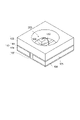
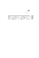
- FIG. 1 is a schematic cross-sectional view showing an embodiment of an optical semiconductor device; FIG. It is a schematic cross section which shows other embodiment of an optical semiconductor device. It is a schematic cross section which shows other embodiment of an optical semiconductor device. 1 is a schematic cross-sectional view showing an embodiment of a copper-clad laminate; FIG. It is a schematic cross section showing an example of an optical semiconductor device produced using a copper-clad laminate. It is a schematic cross section which shows other embodiment of an optical semiconductor device.
- the present invention is not limited to the following embodiments.
- the same elements are denoted by the same reference numerals, and overlapping descriptions are omitted.
- positional relationships such as up, down, left, and right are based on the positional relationships shown in the drawings.
- the dimensional ratios of the drawings are not limited to the illustrated ratios.
- the term “step” includes not only independent steps, but also if the intended action of the step is achieved even if it cannot be clearly distinguished from other steps.
- the term “layer” includes not only a shape structure formed over the entire surface but also a shape structure formed partially when observed as a plan view.
- a numerical range indicated using "-" indicates a range that includes the numerical values before and after "-" as the minimum and maximum values, respectively.
- the upper limit value or lower limit value of the numerical range at one step may be replaced with the upper limit value or lower limit value of the numerical range at another step.
- the upper or lower limits of the numerical ranges may be replaced with the values shown in the examples.
- “A or B” may include either A or B, or may include both.
- the light-reflecting thermosetting resin composition contains an epoxy resin, a curing agent, a benzoxazole compound having a fluorescence intensity of 410 to 500 nm, inorganic hollow particles, and a white pigment.
- epoxy resin an epoxy resin generally used as an epoxy resin molding material for encapsulating electronic parts can be used.
- the thermosetting resin composition according to the present embodiment can form a cured product having high thermal hardness and bending strength and improved mechanical properties.
- epoxy resins include epoxy resins obtained by epoxidizing novolac resins of phenols and aldehydes, such as phenol novolak type epoxy resins and ortho-cresol novolak type epoxy resins; glycidyl ethers; glycidylamine type epoxy resins obtained by reacting polyamines such as diaminodiphenylmethane and isocyanuric acid with epichlorohydrin; linear aliphatic epoxy resins obtained by oxidizing olefin bonds with peracids such as peracetic acid; and alicyclic family epoxy resins. You may use an epoxy resin individually by 1 type or in combination of 2 or more types.
- Epoxy resins are diglycidyl isocyanurate, triglycidyl isocyanurate, bisphenol A type epoxy resin, bisphenol F type epoxy resin, bisphenol S type epoxy resin, 1,2-cyclohexanedicarboxylic acid, 1,3- Dicarboxylic acid diglycidyl esters derived from cyclohexanedicarboxylic acid or 1,4-cyclohexanedicarboxylic acid may be included.
- diglycidyl esters of dicarboxylic acids such as phthalic acid, tetrahydrophthalic acid, hexahydrophthalic acid, methyltetrahydrophthalic acid, nadic acid and methylnadic acid are also suitable as epoxy resins.
- the epoxy resin may contain glycidyl esters such as nucleus-hydrogenated trimellitic acid and nucleus-hydrogenated pyromellitic acid having an alicyclic structure in which the aromatic ring is hydrogenated.
- the epoxy resin may include a polyorganosiloxane having an epoxy group, which is produced by hydrolyzing and condensing a silane compound by heating it in the presence of an organic solvent, an organic base and water.
- a commercially available epoxy resin may be used.
- 3,4-epoxycyclohexylmethyl-3',4'-epoxycyclohexane carboxylate include, for example, Daicel's trade names "Celoxide 2021", “Celoxide 2021A” and “Celoxide 2021P” of Dow Chemical Japan Co., Ltd. It is available under the tradenames "ERL4221", “ERL4221D” and "ERL4221E”.
- As bis(3,4-epoxycyclohexylmethyl)adipate for example, the trade name “ERL4299” from Dow Chemical Japan and the trade name “EXA-7015” from DIC Corporation are available.
- curing agent curing agents generally used in epoxy resin molding materials for encapsulating electronic parts can be used.
- the curing agent is not particularly limited as long as it reacts with the epoxy resin to obtain a cured product, but a less colored curing agent is preferable, and a colorless or pale yellow curing agent is more preferable.
- examples of curing agents include acid anhydride-based curing agents, isocyanuric acid derivative-based curing agents, and phenol-based curing agents. Curing agents may be used singly or in combination of two or more.
- acid anhydride curing agents examples include phthalic anhydride, maleic anhydride, trimellitic anhydride, pyromellitic anhydride, hexahydrophthalic anhydride, tetrahydrophthalic anhydride, methyl nadic anhydride, nadic anhydride, and glutaric anhydride.
- acid dimethylglutaric anhydride, diethylglutaric anhydride, succinic anhydride, methylhexahydrophthalic anhydride, methyltetrahydrophthalic anhydride, 2,3,6,7-naphthalenetetracarboxylic dianhydride, and two aromatic rings Tetracarboxylic acid dianhydrides having the above are mentioned.
- Examples of tetracarboxylic dianhydrides having two or more aromatic rings include 4,4'-biphthalic anhydride, 4,4'-carbonyldiphthalic anhydride, and 4,4'-sulfonyldiphthalic anhydride. , 4,4′-(hexafluoroisopropylidene)diphthalic anhydride, 4,4′-oxydiphthalic anhydride, 9,9-bis(3,4-dicarboxyphenyl)fluorene dianhydride, and the following formula ( A compound represented by 1) can be mentioned.
- Rx represents a divalent organic group
- n represents an integer of 1-10.
- the divalent organic group may be a divalent saturated hydrocarbon group having a saturated hydrocarbon ring.
- saturated hydrocarbons include cyclobutane, cyclopentane, cyclohexane, cycloheptane, cyclooctane, norbornene, divalent Cyclopentadiene, adamantane, hydrogenated naphthalene, and hydrogenated biphenyl.
- isocyanuric acid derivatives examples include 1,3,5-tris(1-carboxymethyl)isocyanurate, 1,3,5-tris(2-carboxyethyl)isocyanurate, 1,3,5-tris(3- carboxypropyl)isocyanurate, and 1,3-bis(2-carboxyethyl)isocyanurate.
- Phenolic curing agents include, for example, phenol, cresol, resorcinol, catechol, phenols such as bisphenol A, bisphenol F, phenylphenol and aminophenol, and/or naphthols such as ⁇ -naphthol, ⁇ -naphthol and dihydroxynaphthalene.
- Phenol-aralkyl resins synthesized from; aralkyl-type phenol resins such as biphenylene-type phenol-aralkyl resins and naphthol-aralkyl resins; cyclopentadiene-type phenol resin; triphenylmethane-type phenol resin; terpene-modified phenol resin; para-xylylene and/or meta-xylylene-modified phenol resin; melamine-modified phenol resin;
- the content of the curing agent is 10 to 150 parts by mass, 30 to 140 parts by mass, 50 to 130 parts by mass, or 80 to 100 parts by mass with respect to 100 parts by mass of the epoxy resin. It may be 120 parts by mass.
- the mixing ratio of the curing agent is such that the active group (acid anhydride group or hydroxyl group) in the curing agent capable of reacting with the epoxy group is 0.5 to 2.0 equivalents per equivalent of the epoxy group in the epoxy resin. It may be from 0.6 to 1.5 equivalents, or from 0.7 to 1.2 equivalents.
- the amount of the active group is 0.5 equivalent or more, the glass transition temperature of the cured product formed from the thermosetting resin composition becomes high, making it easy to obtain a sufficient elastic modulus.
- the amount of active groups is 2.0 equivalents or less, the strength after curing is less likely to decrease.
- thermosetting resin composition according to the present embodiment contains a benzoxazole compound having a fluorescence intensity of 410 to 500 nm, so that it is difficult to be colored even when used for a long time at high temperatures, and maintains its optical properties.
- a cured product that can be formed can be formed.
- the benzoxazole compound according to this embodiment is a compound that absorbs ultraviolet rays and emits blue fluorescence.
- a benzoxazole-based fluorescent bleaching agent can be used as the benzoxazole compound according to the present embodiment.
- Benzoxazole-based fluorescent bleaching agents have a higher fluorescence intensity near 460 nm than other fluorescent brightening agents (e.g., pyrazoline compounds, coumarin compounds, etc.), so the cured product was exposed to high temperatures for a long time. Even in this case, it becomes easier to suppress the decrease in light reflectance.
- fluorescent brightening agents e.g., pyrazoline compounds, coumarin compounds, etc.
- the content of the benzoxazole compound according to the present embodiment is 0.05 to 5.0 parts by mass with respect to 100 parts by mass of the epoxy resin in order to further suppress the decrease in the light reflectance of the cured product in a high temperature environment. is preferably 0.07 to 3.0 parts by mass, more preferably 0.09 to 1.0 parts by mass, and 0.10 to 0.8 parts by mass is even more preferred.
- the white pigment is used to impart a white color tone to the cured product (molded product) obtained from the thermosetting resin composition according to the present embodiment. It can improve the light reflectance of the body.
- white pigments include rare earth oxides such as yttrium oxide, titanium oxide, zinc oxide, aluminum oxide (alumina), magnesium oxide, antimony oxide, zinc sulfate, and zirconium oxide. You may use these individually by 1 type or in combination of 2 or more types. Since the light reflectivity is further improved, the white pigment preferably contains at least one selected from the group consisting of titanium oxide, zinc oxide, alumina, magnesium oxide, antimony oxide, and zirconium oxide. More preferably, it contains at least one selected from the group consisting of antimony and zirconium oxide.
- the median particle size of the white pigment is 0.05 ⁇ m or more, 0.06 ⁇ m or more, 0.08 ⁇ m or more, or 0.10 ⁇ m or more, because the white pigment is easily dispersed uniformly when preparing the thermosetting resin composition.
- the median particle diameter of the white pigment may be 10 ⁇ m or less, 8 ⁇ m or less, 5 ⁇ m or less, 3 ⁇ m or less, or 1 ⁇ m or less, since the light reflection properties of the cured product can be easily improved.
- the median particle size of the white pigment may be, for example, 0.05-10 ⁇ m, 0.06-8 ⁇ m, 0.08-5 ⁇ m, 0.10-3 ⁇ m, or 0.10-1 ⁇ m.
- the median particle diameter can be obtained as the mass average value D50 (or median diameter) in particle size distribution measurement by laser light diffraction method.
- the content of the white pigment is preferably 100 to 400 parts by mass, more preferably 150 to 350 parts by mass, more preferably 200 to 400 parts by mass, based on 100 parts by mass of the epoxy resin, because it further increases the light reflectance. It is more preferably 300 parts by mass.
- thermosetting resin composition according to this embodiment contains inorganic hollow particles as an inorganic filler.
- Inorganic hollow particles are particles having voids inside. Inorganic hollow particles refract and reflect incident light on the surfaces and inner walls, so that combined use with a white pigment makes it possible to form a cured product with further improved light reflectivity and mechanical properties.
- inorganic hollow particles include sodium silicate glass, aluminum silicate glass, sodium borosilicate glass, and shirasu (white sand).
- the outer shell of the inorganic hollow particles is at least selected from the group consisting of sodium silicate glass, aluminum silicate glass, sodium borosilicate glass, shirasu, crosslinked styrene resins, and crosslinked acrylic resins. It is preferably composed of one material, and more preferably composed of at least one material selected from the group consisting of sodium silicate glass, aluminum silicate glass, borosilicate soda glass, and shirasu.
- the median particle size of the inorganic hollow particles may be 1 ⁇ m or more, 5 ⁇ m or more, 8 ⁇ m or more, or 10 ⁇ m or more because the inorganic hollow particles are easily dispersed uniformly when the thermosetting resin composition is prepared.
- the median particle diameter of the inorganic hollow particles may be 25 ⁇ m or less, 24 ⁇ m or less, 22 ⁇ m or less, or 20 ⁇ m or less, since the light reflection properties of the cured product can be easily improved.
- the median particle size of the inorganic hollow particles may be, for example, 1-25 ⁇ m, 5-24 ⁇ m, 8-22 ⁇ m, or 10-20 ⁇ m.
- the outer shell thickness of the inorganic hollow particles is 0.4 to 1.3 ⁇ m, 0.45 to 1.2 ⁇ m, 0.5 to 1.1 ⁇ m, Or it may be 0.55 to 1.0 ⁇ m.
- the inorganic hollow particles have a bulk density of 0.20 to 0.36 g/cm 3 , 0.25 to 0.35 g/cm 3 , or 0.26 to 0.34 g/cm 3 . It can be 3 .
- the bulk density is a density calculated by filling a container with a certain volume with inorganic hollow particles and using the internal volume as the volume.
- the true density of the inorganic hollow particles is 0.40 to 0.75 g/cm 3 , 0.45 to 0.70 g/cm 3 , or 0.50 to 0.75 g/cm 3 . It may be 0.65 g/cm 3 . True density can be measured according to ASTM D2840.
- the pressure resistance of the inorganic hollow particles at 25°C may be 100 MPa or higher, 110 MPa or higher, 125 MPa or higher, or 150 MPa or higher in order to improve the strength of the cured product of the thermosetting resin composition.
- the pressure resistance strength of the inorganic hollow particles at 25° C. may be 500 MPa or less, 300 MPa or less, or 200 MPa or less.
- the compressive strength can be measured according to ASTM D3102.
- the content of the inorganic hollow particles is preferably 100 to 200 parts by mass, more preferably 120 to 180 parts by mass with respect to 100 parts by mass of the epoxy resin, in order to further improve the light reflectance of the cured product. More preferably, 140 to 160 parts by mass is even more preferable.
- thermosetting resin composition according to the present embodiment may contain an inorganic filler other than the inorganic hollow particles from the viewpoint of improving moldability.
- inorganic fillers other than inorganic hollow particles include quartz, fumed silica, precipitated silica, silicic anhydride, fused silica, crystalline silica, ultrafine amorphous silica, barium sulfate, magnesium carbonate, barium carbonate, water.
- the inorganic filler may contain fused silica.
- the median particle size of the fused silica may be 0.1 to 100 ⁇ m, 1 to 50 ⁇ m, 1 to 40 ⁇ m, or 1 to 30 ⁇ m from the viewpoint of improving the packing property with the white pigment.
- the thermosetting resin composition according to this embodiment may contain a curing accelerator in order to accelerate the curing reaction of the epoxy resin.
- Curing accelerators include, for example, amine compounds, imidazole compounds, organophosphorus compounds, alkali metal compounds, alkaline earth metal compounds, and quaternary ammonium salts.
- amine compounds, imidazole compounds, or an organic phosphorus compound it is preferable to use an amine compound, an imidazole compound, or an organic phosphorus compound, and more preferable to use an organic phosphorus compound, from the viewpoint of further improving light reflectivity.
- a hardening accelerator may be used individually by 1 type or in combination of 2 or more types.
- Examples of amine compounds include 1,8-diaza-bicyclo[5.4.0]undecene-7, triethylenediamine, and tri-2,4,6-dimethylaminomethylphenol.
- Examples of imidazole compounds include 2-ethyl-4-methylimidazole.
- organophosphorus compounds include triphenylphosphine, tetraphenylphosphonium tetraphenylborate, tetra-n-butylphosphonium-o,o-diethylphosphorodithioate, tetra-n-butylphosphonium-tetrafluoroborate, and tetra- and n-butylphosphonium-tetraphenylborate.
- the content of the curing accelerator in the thermosetting resin composition is 0.1 to 5.0 parts by mass, 0.5 to 4.0 parts by mass, or 1.0 to 1.0 parts by mass with respect to 100 parts by mass of the epoxy resin. It may be 3.0 parts by mass.
- the content of the curing accelerator is 0.1 parts by mass or more, a sufficient curing acceleration effect is likely to be obtained, and when it is 5.0 parts by mass or less, discoloration of the cured product is easily suppressed.
- a coupling agent may be added to the thermosetting resin composition in order to improve the adhesion between the inorganic filler and the epoxy resin.
- Examples of coupling agents include, but are not limited to, silane coupling agents and titanate-based coupling agents.
- Silane coupling agents include, for example, epoxysilane compounds, aminosilane compounds, cationic silane compounds, vinylsilane compounds, acrylsilane compounds, and mercaptosilane compounds.
- the content of the coupling agent may be 5% by mass or less based on the total amount of the thermosetting resin composition.
- Additives such as antioxidants, release agents, dispersants, and ion scavengers may be added to the thermosetting resin composition according to the present embodiment, if necessary.
- thermosetting resin composition according to this embodiment can be produced by uniformly dispersing and mixing the various components described above. Production means, conditions, etc. are not particularly limited.
- a general method for producing a thermosetting resin composition there is a method of kneading each component with a kneader, roll, extruder, kneader, or a planetary mixer combining rotation and revolution. When kneading each component, it is preferable to carry out in a molten state from the viewpoint of improving dispersibility.
- the kneading conditions may be appropriately determined according to the type or blending amount of each component. For example, kneading at 15 to 100° C. for 5 to 40 minutes is preferable, and kneading at 20 to 100° C. for 10 to 30 minutes is more preferable. preferable.
- the kneading temperature is 15° C. or higher, each component can be easily kneaded and the dispersibility can be improved.
- the kneading temperature is 100° C. or lower, it is possible to suppress the epoxy resin from increasing in molecular weight and curing during kneading.
- the kneading time is 5 minutes or longer, a sufficient dispersing effect is likely to be obtained.
- the kneading time is 40 minutes or less, it is possible to prevent the epoxy resin from increasing in molecular weight and curing during kneading.
- thermosetting resin composition according to the present embodiment is an optical semiconductor element mounting substrate material that requires high light reflectivity and heat resistance, an electrical insulating material, an optical semiconductor sealing material, an adhesive material, a coating material, transfer molding It is useful in various applications such as epoxy resin molding materials for An example of using the thermosetting resin composition according to the present embodiment as an epoxy resin molding material for transfer molding will be described below.
- the bending strength when the thermosetting resin composition according to the present embodiment is transfer molded under conditions of a mold temperature of 180° C., a molding pressure of 6.9 MPa, and a curing time of 90 seconds is It is preferably 70 MPa or more at 25° C., more preferably 75 MPa or more.
- the bending strength is 70 MPa or more, the toughness is excellent.
- the initial light reflectance at a wavelength of 460 nm of the cured product of the thermosetting resin composition according to the present embodiment is preferably 93% or more, and is 94% or more. is more preferable, and 95% or more is even more preferable.
- the light reflectance at a wavelength of 460 nm after heat treatment of the cured product at 150 ° C. for 1008 hours is preferably 86% or more, more preferably 87% or more. It is more preferably 88% or more.
- an L * a * b * color system can be used as a method of quantifying the color difference of the cured product of the thermosetting resin composition according to the present embodiment.
- the b value can be measured according to JIS Z 8781-4. From the viewpoint of ensuring reflectance, the b value of the cured product of the thermosetting resin composition may be 2.00 or less, 1.80 or less, or 1.60 or less. From the viewpoint of ensuring heat resistance, the b value after heat-treating the cured product at 150° C. for 1008 hours may be 6.60 or less, 6.40 or less, or 6.20 or less.
- the substrate for mounting an optical semiconductor element of the present embodiment comprises a cured product of the thermosetting resin composition for light reflection of the present embodiment.
- another embodiment of the substrate for mounting an optical semiconductor element has a concave portion composed of a bottom surface and a wall surface.
- the bottom surface of the recess is a mounting portion for an optical semiconductor element (optical semiconductor element mounting region), and the wall surface of the recess, that is, at least a part of the inner peripheral side surface of the recess is cured with the thermosetting resin composition for light reflection of the present embodiment. It includes things.
- FIG. 1 is a perspective view showing one embodiment of a substrate for mounting an optical semiconductor element.
- the optical semiconductor element mounting substrate of FIG. 1 includes a substrate, and first connection terminals and second connection terminals provided on the substrate, and the first connection terminals and the second connection terminals are connected to each other. It has a cured product of the light-reflecting thermosetting resin composition of the present embodiment between them. More specifically, the optical semiconductor element mounting substrate 110 includes metal wiring 105 (first connection terminal and second connection terminal) on which Ni/Ag plating 104 is formed, and metal wiring 105 (first connection terminal). and a reflector 103, the metal wiring 105 formed with Ni/Ag plating 104, the insulating resin molded body 103' and the reflector.
- the bottom surface of the concave portion 200 is composed of the metal wiring 105 with the Ni/Ag plating 104 formed thereon and the insulating resin molding 103 ′, and the wall surface of the concave portion 200 is composed of the reflector 103 .
- the reflector 103 and the insulating resin molded body 103' are molded bodies made of the cured thermosetting resin composition for light reflection according to the present embodiment.
- FIG. 2 is a schematic diagram showing an embodiment of a process for manufacturing a substrate for mounting an optical semiconductor element.
- the substrate for mounting an optical semiconductor element is formed by, for example, punching out from a metal foil, forming metal wiring 105 by a known method such as etching, applying Ni/Ag plating 104 by electroplating (FIG. 2(a)), and then a step of placing the metal wiring 105 in a mold 151 having a predetermined shape, injecting a thermosetting resin composition for light reflection from a resin injection port 150 of the mold 151, and performing transfer molding under predetermined conditions (see FIG.
- an optical semiconductor element mounting region (recess) 200 surrounded by a reflector 103 made of a cured product of a light reflecting thermosetting resin composition is formed on the optical semiconductor element mounting substrate.
- the bottom surface of the concave portion 200 is composed of the metal wiring 105 serving as the first connection terminal, the metal wiring 105 serving as the second connection terminal, and the cured product of the light-reflecting thermosetting resin composition provided between them. and an insulating resin molded body 103'.
- the transfer molding conditions are as follows: mold temperature is preferably 170 to 200° C., more preferably 170 to 190° C.; molding pressure is preferably 0.5 to 20 MPa, more preferably 2 to 8 MPa; 120 seconds, 1 to 3 hours at an after cure temperature of 120° C. to 180° C. are preferable.
- An optical semiconductor device includes the optical semiconductor element mounting substrate and an optical semiconductor element mounted on the optical semiconductor element mounting substrate.
- the substrate for mounting an optical semiconductor element the optical semiconductor element provided in the concave portion of the substrate for mounting an optical semiconductor element, and the phosphor-containing encapsulant that fills the concave portion to seal the optical semiconductor element.
- an optical semiconductor device including a stopping resin portion the substrate for mounting an optical semiconductor element, the optical semiconductor element provided in the concave portion of the substrate for mounting an optical semiconductor element, and the phosphor-containing encapsulant that fills the concave portion to seal the optical semiconductor element.
- FIG. 3 is a perspective view showing an embodiment in which the optical semiconductor element 100 is mounted on the substrate 110 for mounting an optical semiconductor element.
- the optical semiconductor element 100 is mounted at a predetermined position in an optical semiconductor element mounting region (concave portion) 200 of an optical semiconductor element mounting substrate 110, and is electrically connected to a metal wiring 105 and a bonding wire 102.
- 4 and 5 are schematic cross-sectional views showing an embodiment of the optical semiconductor device.
- the optical semiconductor device includes an optical semiconductor element mounting substrate 110, an optical semiconductor element 100 provided at a predetermined position in a recess 200 of the optical semiconductor element mounting substrate 110, and a recess 200.
- 105 are electrically connected by bonding wires 102 or solder bumps 107 .
- FIG. 6 is also a schematic cross-sectional view showing one embodiment of the optical semiconductor device.
- the LED element 300 is arranged at a predetermined position on the lead 304 on which the reflector 303 is formed via the die bonding material 306, and the LED element 300 and the lead 304 are electrically connected by the bonding wire 301.
- the LED element 300 is sealed with a transparent sealing resin 302 that is connected and contains a phosphor 305 .
- the light-reflecting thermosetting resin composition of the present embodiment can be used, for example, as a light-reflecting coating agent for copper-clad laminates, substrates for mounting optical semiconductor elements, optical semiconductor elements, and the like.
- a copper-clad laminate according to the present embodiment includes a light-reflecting resin layer formed using the light-reflecting thermosetting resin composition described above, and a copper foil laminated on the light-reflecting resin layer. .
- FIG. 7 is a schematic cross-sectional view showing a preferred embodiment of a copper-clad laminate.
- a copper clad laminate 400 includes a base material 401, a light reflecting resin layer 402 laminated on the base material 401, and a copper foil 403 laminated on the light reflecting resin layer 402. , is equipped with
- the light reflecting resin layer 402 is formed using the light reflecting thermosetting resin composition described above.
- a base material used for a copper-clad laminate can be used without particular limitation, and examples thereof include a resin laminate such as an epoxy resin laminate and a substrate for mounting an optical semiconductor.
- the copper-clad laminate 400 is produced, for example, by applying the light-reflecting thermosetting resin composition of the present embodiment to the surface of the substrate 401, overlaying the copper foil 403, and heating and pressurizing to cure the thermosetting resin composition.
- thermosetting resin composition As a method for applying the thermosetting resin composition to the substrate 401, for example, a printing method, a die coating method, a curtain coating method, a spray coating method, a roll coating method, or the like can be used.
- the thermosetting resin composition may contain a solvent so as to facilitate application.
- a solvent it is preferable to set the total amount excluding the solvent when the total amount of the thermosetting resin composition is based on the mixing ratio of each component described above.
- the conditions for heating and pressurization are not particularly limited, but for example, it is preferable to perform heating and pressurization under conditions of 130 to 180° C., 0.5 to 4 MPa, and 30 to 600 minutes.
- the reflective resin layer 402 and the copper foil 403 may be laminated respectively.
- the copper-clad laminate may be composed only of the light reflecting resin layer 402 and the copper foil 403 without using the base material 401 .
- the light reflecting resin layer 402 will play a role as a base material.
- the light reflecting resin layer 402 can be obtained by impregnating a glass cloth or the like with the present thermosetting resin composition and curing the composition.
- FIG. 8 is a schematic cross-sectional view showing an example of an optical semiconductor device produced using a copper-clad laminate.
- the optical semiconductor device 500 is a surface-mounted light-emitting diode that includes an optical semiconductor element 410 and a transparent sealing resin 404 provided to seal the optical semiconductor element 410.
- optical semiconductor element 410 is adhered to copper foil 403 via adhesive layer 408 and electrically connected to copper foil 403 by bonding wire 409 .
- a substrate for mounting an optical semiconductor element As another embodiment of a substrate for mounting an optical semiconductor element, a light-reflecting resin layer formed between a plurality of conductor members (connection terminals) on a substrate using the above-described light-reflecting thermosetting resin composition.
- An optical semiconductor element mounting substrate provided with the optical semiconductor element may be mentioned.
- Another embodiment of an optical semiconductor device is obtained by mounting an optical semiconductor element on the above substrate for mounting an optical semiconductor element.
- FIG. 9 is a schematic cross-sectional view showing a preferred embodiment of an optical semiconductor device.
- an optical semiconductor device 600 includes a substrate 601, a plurality of conductor members 602 formed on the surface of the substrate 601, and a plurality of conductor members (connection terminals) formed between the 602,
- An optical semiconductor element 610 is mounted on an optical semiconductor element mounting substrate provided with a light reflecting resin layer 603 containing a cured product of the thermosetting resin composition for light reflection, and the optical semiconductor element 610 is sealed. It is a surface-mounted light-emitting diode in which a transparent sealing resin 604 is provided on the surface.
- optical semiconductor element 610 is adhered to conductor member 602 via adhesive layer 608 and electrically connected to conductor member 602 by bonding wire 609 .
- a base material used for a substrate for mounting an optical semiconductor element can be used without particular limitation, and examples thereof include resin laminates such as epoxy resin laminates.
- the conductor member 602 functions as a connection terminal, and can be formed by a known method such as photoetching a copper foil.
- the substrate for mounting an optical semiconductor element is obtained by applying the light reflecting thermosetting resin composition between the plurality of conductor members 602 on the base material 601 and heating and curing to obtain a cured product of the light reflecting thermosetting resin composition.
- thermosetting resin composition for light reflection may contain a solvent so as to facilitate application.
- a solvent it is preferable to set the total amount of the resin composition excluding the solvent when the mixing ratio of each component described above is based on the total amount of the resin composition.
- the heating conditions for heat-curing the coating film of the thermosetting resin composition for light reflection are not particularly limited.
- the conductor member 602 may be subjected to roughening treatment such as oxidation-reduction treatment, CZ treatment (manufactured by MEC Co., Ltd.).
- the substrate for mounting an optical semiconductor element and the optical semiconductor device having the cured product of the thermosetting resin composition for light reflection according to the present embodiment have high light reflectance, and even when used at high temperatures for a long time, the optical properties are maintained. can be maintained.
- thermosetting resin composition for light reflection In order to prepare the light-reflecting thermosetting resin compositions of Examples and Comparative Examples, the following components were prepared.
- thermosetting resin composition for light reflection.
- the light-reflecting thermosetting resin composition was transfer-molded under conditions of a mold temperature of 180°C, a molding pressure of 6.9 MPa, and a curing time of 90 seconds, and then post-cured at 150°C for 2 hours to obtain a thickness of 3.
- a 0 mm test piece was produced.
- CM-600d manufactured by Konica Minolta, Inc.
- the light reflectance of the test piece at a wavelength of 460 nm was measured.
- the light reflectance was measured after the test piece was allowed to stand in a constant temperature bath set at 150° C. for 1008 hours.
- b value The b value was calculated using a spectrophotometer "CM-600d" for the test piece prepared by the above light reflectance measurement.
- the light-reflecting thermosetting resin compositions of Examples are capable of forming cured products (molded products) having high initial light reflectance and excellent light reflectivity even when used at high temperatures for a long time. can be confirmed.
- SYMBOLS 100 Optical-semiconductor element, 101... Encapsulation resin, 102... Bonding wire, 103... Reflector, 103'... Insulating resin molding, 104... Ni/Ag plating, 105... Metal wiring, 106... Phosphor, 107... Solder Bump 110 Optical semiconductor element mounting substrate 150 Resin injection port 151 Mold 200 Optical semiconductor element mounting area 300 LED element 301 Bonding wire 302 Sealing resin 303 Reflector DESCRIPTION OF SYMBOLS 304... Lead, 305... Phosphor, 306... Die-bonding material, 400... Copper-clad laminate, 401... Base material, 402... Light reflecting resin layer, 403... Copper foil, 404...
- Sealing resin 408... Adhesive layer, 409 ... Bonding wire 410 ... Optical semiconductor element 500, 600 ... Optical semiconductor device 601 ... Base material 602 ... Conductor member 603 ... Light reflecting resin layer 604 . Sealing resin 608 ... Adhesive layer 609 ... Bonding wire , 610 . . . optical semiconductor elements.
Abstract
本開示の一側面は、エポキシ樹脂、硬化剤、410~500nmに蛍光強度を有するベンゾオキサゾール化合物、無機中空粒子、及び白色顔料を含有する、光反射用熱硬化性樹脂組成物に関する。
Description
本開示は、光反射用熱硬化性樹脂組成物、光半導体素子搭載用基板及び光半導体装置に関する。
LED(Light Emitting Diode:発光ダイオード)等の光半導体素子と蛍光体とを組み合わせた光半導体装置は、エネルギー効率が高く、寿命が長いことから、屋外用ディスプレイ、携帯液晶バックライト、車載用途等の様々な用途に使用され、その需要が拡大している。これに伴い、LEDデバイスの高輝度化が進んでおり、素子の発熱量増大によるジャンクション温度の上昇、又は、直接的な光エネルギーの増大による光半導体装置の劣化を防ぐことが求められている。
特許文献1には、樹脂硬化後の可視光から近紫外光領域において高い反射率を有する熱硬化性樹脂組成物を用いた光半導体素子搭載用基板が開示されている。また、特許文献2には、光漏れを低減した光半導体素子搭載用部材が開示されている。
一般に、熱硬化性樹脂組成物を用いてLEDのリフレクターを形成する際には、トランスファーモールド成形が用いられている。熱硬化性樹脂組成物から形成される硬化物には、光反射率をより高めるだけでなく、高温下で長時間使用された際にも光学特性を維持できることが求められる。
本開示は、高温下で長時間使用された際にも光反射性に優れる硬化物を形成できる光反射用熱硬化性樹脂組成物、これを用いた光半導体素子搭載用基板及び光半導体装置を提供することを目的とする。
本開示の一態様は、以下の光反射用熱硬化性樹脂組成物、光半導体素子搭載用基板、及び光半導体装置に関する。
[1]エポキシ樹脂、硬化剤、410~500nmに蛍光強度を有するベンゾオキサゾール化合物、無機中空粒子、及び白色顔料を含有する、光反射用熱硬化性樹脂組成物。
[2]前記ベンゾオキサゾール化合物の含有量が、前記エポキシ樹脂100質量部に対して0.05~5.0質量部である、上記[1]に記載の光反射用熱硬化性樹脂組成物。
[3]前記無機中空粒子の含有量が、前記エポキシ樹脂100質量部に対して100~200質量部である、上記[1]又は[2]に記載の光反射用熱硬化性樹脂組成物。
[4]前記無機中空粒子の中心粒径が、1~25μmである、上記[1]~[3]のいずれかに記載の光反射用熱硬化性樹脂組成物。
[5]前記白色顔料が、酸化チタン、酸化亜鉛、アルミナ、酸化マグネシウム、酸化アンチモン、及び酸化ジルコニウムからなる群より選ばれる少なくとも1種を含む、上記[1]~[4]のいずれかに記載の光反射用熱硬化性樹脂組成物。
[6]上記[1]~[5]のいずれかに記載の光反射用熱硬化性樹脂組成物の硬化物を備える、光半導体素子搭載用基板。
[7]底面及び壁面から構成される凹部を有し、当該凹部の前記底面が光半導体素子の搭載部であり、前記凹部の前記壁面の少なくとも一部が、上記[1]~[5]のいずれかに記載の光反射用熱硬化性樹脂組成物の硬化物を含む、光半導体素子搭載用基板。
[8]基板と、当該基板上に設けられた第1の接続端子及び第2の接続端子とを備え、前記第1の接続端子と前記第2の接続端子との間に、上記[1]~[5]のいずれかに記載の光反射用熱硬化性樹脂組成物の硬化物を有する、光半導体素子搭載用基板。
[9]上記[6]~[8]のいずれかに記載の光半導体素子搭載用基板と、当該光半導体素子搭載用基板に搭載された光半導体素子と、を有する、光半導体装置。
本開示によれば、高温下で長時間使用された際にも光反射性に優れる硬化物を形成できる光反射用熱硬化性樹脂組成物、これを用いた光半導体素子搭載用基板及び光半導体装置を提供することができる。
以下、必要に応じて図面を参照しつつ、本開示の好適な実施形態について詳細に説明する。ただし、本発明は以下の実施形態に限定されない。なお、図面中、同一要素には同一符号を付すこととし、重複する説明は省略する。また、上下左右等の位置関係は、特に断らない限り、図面に示す位置関係に基づくものとする。さらに、図面の寸法比率は図示の比率に限られない。本明細書において、「工程」との語は、独立した工程だけではなく、他の工程と明確に区別できない場合であってもその工程の所期の作用が達成されれば、本用語に含まれる。本明細書において、「層」との語は、平面図として観察したときに、全面に形成されている形状の構造に加え、一部に形成されている形状の構造も包含される。
本明細書において、「~」を用いて示された数値範囲は、「~」の前後に記載される数値をそれぞれ最小値及び最大値として含む範囲を示す。本明細書に段階的に記載されている数値範囲において、ある段階の数値範囲の上限値又は下限値は、他の段階の数値範囲の上限値又は下限値に置き換えてもよい。本明細書に記載されている数値範囲において、その数値範囲の上限値又は下限値は、実施例に示されている値に置き換えてもよい。「A又はB」とは、A及びBのどちらか一方を含んでいればよく、両方とも含んでいてもよい。本明細書に例示する材料は、特に断らない限り、1種を単独で又は2種以上を組み合わせて用いることができる。
[光反射用熱硬化性樹脂組成物]
本実施形態に係る光反射用熱硬化性樹脂組成物は、エポキシ樹脂、硬化剤、410~500nmに蛍光強度を有するベンゾオキサゾール化合物、無機中空粒子、及び白色顔料を含有する。
本実施形態に係る光反射用熱硬化性樹脂組成物は、エポキシ樹脂、硬化剤、410~500nmに蛍光強度を有するベンゾオキサゾール化合物、無機中空粒子、及び白色顔料を含有する。
(エポキシ樹脂)
エポキシ樹脂としては、電子部品封止用エポキシ樹脂成形材料で一般に使用されているエポキシ樹脂を用いることができる。本実施形態に係る熱硬化性樹脂組成物は、エポキシ樹脂を含有することで、熱時硬度及び曲げ強度が高く、機械的特性を向上した硬化物を形成することができる。エポキシ樹脂として、例えば、フェノールノボラック型エポキシ樹脂、オルソクレゾールノボラック型エポキシ樹脂等のフェノール類とアルデヒド類のノボラック樹脂をエポキシ化したエポキシ樹脂;ビスフェノールA、ビスフェノールF、ビスフェノールS、アルキル置換ビスフェノール等のジグリシジルエーテル;ジアミノジフェニルメタン、イソシアヌル酸等のポリアミンとエピクロルヒドリンとの反応により得られるグリシジルアミン型エポキシ樹脂;オレフィン結合を過酢酸等の過酸で酸化して得られる線状脂肪族エポキシ樹脂;及び脂環族エポキシ樹脂が挙げられる。エポキシ樹脂は、1種を単独で又は2種以上を組み合わせて用いてもよい。
エポキシ樹脂としては、電子部品封止用エポキシ樹脂成形材料で一般に使用されているエポキシ樹脂を用いることができる。本実施形態に係る熱硬化性樹脂組成物は、エポキシ樹脂を含有することで、熱時硬度及び曲げ強度が高く、機械的特性を向上した硬化物を形成することができる。エポキシ樹脂として、例えば、フェノールノボラック型エポキシ樹脂、オルソクレゾールノボラック型エポキシ樹脂等のフェノール類とアルデヒド類のノボラック樹脂をエポキシ化したエポキシ樹脂;ビスフェノールA、ビスフェノールF、ビスフェノールS、アルキル置換ビスフェノール等のジグリシジルエーテル;ジアミノジフェニルメタン、イソシアヌル酸等のポリアミンとエピクロルヒドリンとの反応により得られるグリシジルアミン型エポキシ樹脂;オレフィン結合を過酢酸等の過酸で酸化して得られる線状脂肪族エポキシ樹脂;及び脂環族エポキシ樹脂が挙げられる。エポキシ樹脂は、1種を単独で又は2種以上を組み合わせて用いてもよい。
着色が少ないことから、エポキシ樹脂は、ジグリシジルイソシアヌレート、トリグリシジルイソシアヌレート、ビスフェノールA型エポキシ樹脂、ビスフェノールF型エポキシ樹脂、ビスフェノールS型エポキシ樹脂、1,2-シクロヘキサンジカルボン酸、1,3-シクロヘキサンジカルボン酸又は1,4-シクロヘキサンジカルボン酸から誘導されるジカルボン酸ジグリシジルエステルを含んでよい。同様の理由から、エポキシ樹脂としては、フタル酸、テトラヒドロフタル酸、ヘキサヒドロフタル酸、メチルテトラヒドロフタル酸、ナジック酸、メチルナジック酸等のジカルボン酸のジグリシジルエステルも好適である。エポキシ樹脂は、芳香環が水素化された脂環式構造を有する核水素化トリメリット酸、核水素化ピロメリット酸等のグリシジルエステルを含んでよい。エポキシ樹脂は、シラン化合物を有機溶媒、有機塩基及び水の存在下に加熱して、加水分解して縮合させることにより製造される、エポキシ基を有するポリオルガノシロキサンを含んでもよい。
エポキシ樹脂は、市販品を使用してもよい。3,4-エポキシシクロヘキシルメチル-3’,4’-エポキシシクロヘキサンカルボキシレートとして、例えば、株式会社ダイセルの商品名「セロキサイド2021」、「セロキサイド2021A」及び「セロキサイド2021P」、ダウ・ケミカル日本株式会社の商品名「ERL4221」、「ERL4221D」及び「ERL4221E」を入手できる。ビス(3,4-エポキシシクロヘキシルメチル)アジペートとして、例えば、ダウ・ケミカル日本株式会社の商品名「ERL4299」、DIC株式会社の商品名「EXA-7015」を入手できる。1-エポキシエチル-3,4-エポキシシクロヘキサン又はリモネンジエポキシドとして、例えば、三菱ケミカル株式会社の商品名「jER YX8000」、「jER YX8034」及び「jER YL7170」、株式会社ダイセルの商品名「セロキサイド2081」、「セロキサイド3000」、「エポリードGT301」、「エポリードGT401」及び「EHPE3150」を入手できる。トリスグリシジルイソシアヌレートとして、例えば、日産化学工業株式会社の商品名「TEPIC-S」を入手できる。
(硬化剤)
硬化剤としては、電子部品封止用エポキシ樹脂成形材料で一般に使用されている硬化剤を用いることができる。硬化剤は、エポキシ樹脂と反応して硬化物が得られるものであれば、特に限定されないが、着色の少ない硬化剤が好ましく、無色又は淡黄色の硬化剤がより好ましい。硬化剤としては、例えば、酸無水物系硬化剤、イソシアヌル酸誘導体系硬化剤、及びフェノール系硬化剤が挙げられる。硬化剤は、1種を単独で又は2種以上を組み合わせて用いてもよい。
硬化剤としては、電子部品封止用エポキシ樹脂成形材料で一般に使用されている硬化剤を用いることができる。硬化剤は、エポキシ樹脂と反応して硬化物が得られるものであれば、特に限定されないが、着色の少ない硬化剤が好ましく、無色又は淡黄色の硬化剤がより好ましい。硬化剤としては、例えば、酸無水物系硬化剤、イソシアヌル酸誘導体系硬化剤、及びフェノール系硬化剤が挙げられる。硬化剤は、1種を単独で又は2種以上を組み合わせて用いてもよい。
酸無水物系硬化剤としては、例えば、無水フタル酸、無水マレイン酸、無水トリメリット酸、無水ピロメリット酸、ヘキサヒドロ無水フタル酸、テトラヒドロ無水フタル酸、無水メチルナジック酸、無水ナジック酸、無水グルタル酸、無水ジメチルグルタル酸、無水ジエチルグルタル酸、無水コハク酸、メチルヘキサヒドロ無水フタル酸、メチルテトラヒドロ無水フタル酸、2,3,6,7-ナフタレンテトラカルボン酸二無水物、及び芳香環を2以上有するテトラカルボン酸二無水物が挙げられる。
芳香環を2以上有するテトラカルボン酸二無水物としては、例えば、4,4’-ビフタル酸無水物、4,4’-カルボニルジフタル酸無水物、4,4’-スルホニルジフタル酸無水物、4,4’-(ヘキサフルオロイソプロピリデン)ジフタル酸無水物、4,4’-オキシジフタル酸無水物、9,9-ビス(3,4-ジカルボキシフェニル)フルオレン二無水物、及び下記式(1)で表される化合物が挙げられる。

式(1)中、Rxは、2価の有機基を示し、nは1~10の整数を示す。2価の有機基は、飽和炭化水素環を有する2価の飽和炭化水素基であってよく、飽和炭化水素としては、例えば、シクロブタン、シクロペンタン、シクロヘキサン、シクロへプタン、シクロオクタン、ノルボルネン、ジシクロペンタジエン、アダマンタン、水素化ナフタレン、及び水素化ビフェニルが挙げられる。
イソシアヌル酸誘導体としては、例えば、1,3,5-トリス(1-カルボキシメチル)イソシアヌレート、1,3,5-トリス(2-カルボキシエチル)イソシアヌレート、1,3,5-トリス(3-カルボキシプロピル)イソシアヌレート、及び1,3-ビス(2-カルボキシエチル)イソシアヌレートが挙げられる。
フェノール系硬化剤としては、例えば、フェノール、クレゾール、レゾルシン、カテコール、ビスフェノールA、ビスフェノールF、フェニルフェノール、アミノフェノール等のフェノール類及び/又はα-ナフトール、β-ナフトール、ジヒドロキシナフタレン等のナフトール類と、ホルムアルデヒド、ベンズアルデヒド、サリチルアルデヒド等のアルデヒド類とを酸性触媒下で縮合又は共縮合させて得られる、ノボラック型フェノール樹脂;フェノール類及び/又はナフトール類と、ジメトキシパラキシレン又はビス(メトキシメチル)ビフェニルとから合成されるフェノール・アラルキル樹脂;ビフェニレン型フェノール・アラルキル樹脂、ナフトール・アラルキル樹脂等のアラルキル型フェノール樹脂;フェノール類及び/又はナフトール類と、ジシクロペンタジエンとの共重合によって合成される、ジシクロペンタジエン型フェノール樹脂;トリフェニルメタン型フェノール樹脂;テルペン変性フェノール樹脂;パラキシリレン及び/又はメタキシリレン変性フェノール樹脂;メラミン変性フェノール樹脂;並びにこれら2種以上を共重合して得られるフェノール樹脂が挙げられる。
本実施形態に係る熱硬化性樹脂組成物において、硬化剤の含有量は、エポキシ樹脂100質量部に対して、10~150質量部、30~140質量部、50~130質量部、又は80~120質量部であってよい。
硬化剤の配合割合は、エポキシ樹脂中のエポキシ基1当量に対して、当該エポキシ基と反応可能な硬化剤中の活性基(酸無水物基又は水酸基)が0.5~2.0当量、0.6~1.5当量、又は0.7~1.2当量であってよい。上記活性基が0.5当量以上であると、熱硬化性樹脂組成物から形成される硬化物のガラス転移温度が高くなり、充分な弾性率が得られ易くなる。一方、上記活性基が2.0当量以下であると、硬化後の強度が低下し難くなる。
(410~500nmに蛍光強度を有するベンゾオキサゾール化合物)
本実施形態に係る熱硬化性樹脂組成物は、410~500nmに蛍光強度を有するベンゾオキサゾール化合物を含有することで、高温下で長時間使用された際にも着色し難く、光学特性を維持することができる硬化物を形成することができる。本実施形態に係るベンゾオキサゾール化合物は、紫外線を吸収して青色の蛍光を発する化合物である。本実施形態に係るベンゾオキサゾール化合物としては、例えば、ベンゾオキサゾール系の蛍光漂白剤を用いることができる。ベンゾオキサゾール系の蛍光漂白剤は、他の蛍光増白剤(例えば、ピラゾリン化合物、クマリン化合物等)に比べて、460nm付近での蛍光強度が高いため、硬化物が高温下で長時間晒された場合であっても光反射率の低下を抑制し易くなる。
本実施形態に係る熱硬化性樹脂組成物は、410~500nmに蛍光強度を有するベンゾオキサゾール化合物を含有することで、高温下で長時間使用された際にも着色し難く、光学特性を維持することができる硬化物を形成することができる。本実施形態に係るベンゾオキサゾール化合物は、紫外線を吸収して青色の蛍光を発する化合物である。本実施形態に係るベンゾオキサゾール化合物としては、例えば、ベンゾオキサゾール系の蛍光漂白剤を用いることができる。ベンゾオキサゾール系の蛍光漂白剤は、他の蛍光増白剤(例えば、ピラゾリン化合物、クマリン化合物等)に比べて、460nm付近での蛍光強度が高いため、硬化物が高温下で長時間晒された場合であっても光反射率の低下を抑制し易くなる。
本実施形態に係るベンゾオキサゾール化合物の含有量は、高温環境下における硬化物の光反射率の低下をより抑制する点から、エポキシ樹脂100質量部に対して、0.05~5.0質量部であることが好ましく、0.07~3.0質量部であることがより好ましく、0.09~1.0質量部であることが更に好ましく、0.10~0.8質量部であることがより一層好ましい。
(白色顔料)
白色顔料は、本実施形態に係る熱硬化性樹脂組成物から得られる硬化物(成形体)に白色系の色調を付与するために用いられ、特にその色調を高度の白色とすることにより、成形体の光反射率を向上させることができる。
白色顔料は、本実施形態に係る熱硬化性樹脂組成物から得られる硬化物(成形体)に白色系の色調を付与するために用いられ、特にその色調を高度の白色とすることにより、成形体の光反射率を向上させることができる。
白色顔料としては、例えば、酸化イットリウム等の希土類酸化物、酸化チタン、酸化亜鉛、酸化アルミニウム(アルミナ)、酸化マグネシウム、酸化アンチモン、硫酸亜鉛、及び酸化ジルコニウムが挙げられる。これらは、1種を単独で又は2種以上を組み合わせて用いてもよい。光反射性をより向上することから、白色顔料は、酸化チタン、酸化亜鉛、アルミナ、酸化マグネシウム、酸化アンチモン、及び酸化ジルコニウムからなる群より選ばれる少なくとも1種を含むことが好ましく、酸化チタン、酸化アンチモン、及び酸化ジルコニウムからなる群より選ばれる少なくとも1種を含むことがより好ましい。
白色顔料の中心粒径は、熱硬化性樹脂組成物を調製する際に白色顔料を均一に分散し易いことから、0.05μm以上、0.06μm以上、0.08μm以上、又は0.10μm以上であってよい。白色顔料の中心粒径は、硬化物の光反射特性を向上し易いことから、10μm以下、8μm以下、5μm以下、3μm以下、又は1μm以下であってよい。白色顔料の中心粒径は、例えば、0.05~10μm、0.06~8μm、0.08~5μm、0.10~3μm、又は0.10~1μmであってもよい。本明細書において、中心粒径は、レーザー光回折法による粒度分布測定における質量平均値D50(又はメジアン径)として求めることができる。
白色顔料の含有量は、光反射率をより高めることから、エポキシ樹脂100質量部に対して、100~400質量部であることが好ましく、150~350質量部であることがより好ましく、200~300質量部であることが更に好ましい。
(無機中空粒子)
本実施形態に係る熱硬化性樹脂組成物は、無機充填剤として無機中空粒子を含有する。無機中空粒子は、内部に空隙部を有する粒子である。無機中空粒子は、入射光を表面及び内壁で屈折及び反射するため、白色顔料と併用することで、光反射性及び機械的特性をより一層向上した硬化物を形成することができる。
本実施形態に係る熱硬化性樹脂組成物は、無機充填剤として無機中空粒子を含有する。無機中空粒子は、内部に空隙部を有する粒子である。無機中空粒子は、入射光を表面及び内壁で屈折及び反射するため、白色顔料と併用することで、光反射性及び機械的特性をより一層向上した硬化物を形成することができる。
無機中空粒子としては、例えば、珪酸ソーダガラス、アルミ珪酸ガラス、硼珪酸ソーダガラス、及びシラス(白砂)が挙げられる。耐熱性及び耐圧強度の観点からは、無機中空粒子の外殻は、珪酸ソーダガラス、アルミ珪酸ガラス、硼珪酸ソーダガラス、シラス、架橋スチレン系樹脂、及び架橋アクリル系樹脂からなる群より選ばれる少なくとも1種の材質から構成されることが好ましく、珪酸ソーダガラス、アルミ珪酸ガラス、硼珪酸ソーダガラス、及びシラスからなる群より選ばれる少なくとも1種の材質から構成されることがより好ましい。
無機中空粒子の中心粒径は、熱硬化性樹脂組成物を調製する際に無機中空粒子を均一に分散し易いことから、1μm以上、5μm以上、8μm以上、又は10μm以上であってよい。無機中空粒子の中心粒径は、硬化物の光反射特性を向上し易いことから、25μm以下、24μm以下、22μm以下、又は20μm以下であってよい。無機中空粒子の中心粒径は、例えば、1~25μm、5~24μmm、8~22μm、又は10~20μmであってもよい。
熱硬化性樹脂組成物の機械的特性を向上することから、無機中空粒子の外殻の厚みは、0.4~1.3μm、0.45~1.2μm、0.5~1.1μm、又は0.55~1.0μmであってよい。
光反射性をより向上することから、無機中空粒子のかさ密度は、0.20~0.36g/cm3、0.25~0.35g/cm3、又は0.26~0.34g/cm3であってよい。かさ密度は、ある容積の容器に無機中空粒子を充填し、その内容積を体積として算出した密度である。
光反射性と機械的特性とのバランスに優れることから、無機中空粒子の真密度は、0.40~0.75g/cm3、0.45~0.70g/cm3、又は0.50~0.65g/cm3であってよい。真密度は、ASTM D2840に準拠して測定することができる。
熱硬化性樹脂組成物の硬化物の強度を向上することから、無機中空粒子の耐圧強度は、25℃で100MPa以上、110MPa以上、125MPa以上、又は150MPa以上であってよい。熱硬化性樹脂組成物の成形性を向上することから、無機中空粒子の耐圧強度は、25℃で500MPa以下、300MPa以下、又は200MPa以下であってよい。耐圧強度は、ASTM D3102に準拠して測定することができる。
無機中空粒子の含有量は、硬化物の光反射率をより向上する点から、エポキシ樹脂100質量部に対して、100~200質量部であることが好ましく、120~180質量部であることがより好ましく、140~160質量部であることが更に好ましい。
(無機中空粒子以外の無機充填剤)
本実施形態に係る熱硬化性樹脂組成物は、成形性を向上する観点から、無機中空粒子以外の無機充填剤を含有してよい。無機中空粒子以外の無機充填剤としては、例えば、石英、ヒュームドシリカ、沈降性シリカ、無水ケイ酸、溶融シリカ、結晶性シリカ、超微粉無定型シリカ、硫酸バリウム、炭酸マグネシウム、炭酸バリウム、水酸化アルミニウム、水酸化マグネシウム、チタン酸カリウム、及びケイ酸カルシウムが挙げられる。
本実施形態に係る熱硬化性樹脂組成物は、成形性を向上する観点から、無機中空粒子以外の無機充填剤を含有してよい。無機中空粒子以外の無機充填剤としては、例えば、石英、ヒュームドシリカ、沈降性シリカ、無水ケイ酸、溶融シリカ、結晶性シリカ、超微粉無定型シリカ、硫酸バリウム、炭酸マグネシウム、炭酸バリウム、水酸化アルミニウム、水酸化マグネシウム、チタン酸カリウム、及びケイ酸カルシウムが挙げられる。
成形性の点から、無機充填剤は溶融シリカを含んでよい。溶融シリカの中心粒径は、白色顔料とのパッキング性を向上させる観点から、0.1~100μm、1~50μm、1~40μm、又は1~30μmであってよい。
(硬化促進剤)
本実施形態に係る熱硬化性樹脂組成物は、エポキシ樹脂の硬化反応を促進するために、硬化促進剤を含有してよい。硬化促進剤としては、例えば、アミン化合物、イミダゾール化合物、有機リン化合物、アルカリ金属化合物、アルカリ土類金属化合物、及び第4級アンモニウム塩が挙げられる。これらの硬化促進剤の中でも、光反射性をより向上する観点から、アミン化合物、イミダゾール化合物、又は有機リン化合物を用いることが好ましく、有機リン化合物を用いることがより好ましい。硬化促進剤は、1種を単独で又は2種以上を組み合わせて使用してもよい。
本実施形態に係る熱硬化性樹脂組成物は、エポキシ樹脂の硬化反応を促進するために、硬化促進剤を含有してよい。硬化促進剤としては、例えば、アミン化合物、イミダゾール化合物、有機リン化合物、アルカリ金属化合物、アルカリ土類金属化合物、及び第4級アンモニウム塩が挙げられる。これらの硬化促進剤の中でも、光反射性をより向上する観点から、アミン化合物、イミダゾール化合物、又は有機リン化合物を用いることが好ましく、有機リン化合物を用いることがより好ましい。硬化促進剤は、1種を単独で又は2種以上を組み合わせて使用してもよい。
アミン化合物としては、例えば、1,8-ジアザ-ビシクロ[5.4.0]ウンデセン-7、トリエチレンジアミン、及びトリ-2,4,6-ジメチルアミノメチルフェノールが挙げられる。イミダゾール化合物として、例えば、2-エチル-4-メチルイミダゾールが挙げられる。有機リン化合物としては、例えば、トリフェニルホスフィン、テトラフェニルホスホニウムテトラフェニルボレート、テトラ-n-ブチルホスホニウム-o,o-ジエチルホスホロジチオエート、テトラ-n-ブチルホスホニウム-テトラフルオロボレート、及びテトラ-n-ブチルホスホニウム-テトラフェニルボレートが挙げられる。
熱硬化性樹脂組成物中の硬化促進剤の含有量は、エポキシ樹脂100質量部に対して、0.1~5.0質量部、0.5~4.0質量部、又は1.0~3.0質量部であってよい。硬化促進剤の含有量が、0.1質量部以上であると、十分な硬化促進効果を得られ易く、5.0質量部以下であると、硬化物の変色を抑制し易くなる。
(カップリング剤)
熱硬化性樹脂組成物には、無機充填剤と、エポキシ樹脂との密着性を向上させるために、カップリング剤を添加してよい。カップリング剤としては、特に限定されないが、例えば、シランカップリング剤及びチタネート系カップリング剤が挙げられる。シランカップリング剤としては、例えば、エポキシシラン化合物、アミノシラン化合物、カチオニックシラン化合物、ビニルシラン化合物、アクリルシラン化合物、及びメルカプトシラン化合物が挙げられる。カップリング剤の含有量は、熱硬化性樹脂組成物の全量を基準として、5質量%以下であってよい。
熱硬化性樹脂組成物には、無機充填剤と、エポキシ樹脂との密着性を向上させるために、カップリング剤を添加してよい。カップリング剤としては、特に限定されないが、例えば、シランカップリング剤及びチタネート系カップリング剤が挙げられる。シランカップリング剤としては、例えば、エポキシシラン化合物、アミノシラン化合物、カチオニックシラン化合物、ビニルシラン化合物、アクリルシラン化合物、及びメルカプトシラン化合物が挙げられる。カップリング剤の含有量は、熱硬化性樹脂組成物の全量を基準として、5質量%以下であってよい。
本実施形態に係る熱硬化性樹脂組成物には、必要に応じて、酸化防止剤、離型剤、分散剤、イオン捕捉剤等の添加剤を添加してよい。
本実施形態に係る熱硬化性樹脂組成物は、上述した各種成分を均一に分散し混合することで作製することができる。作製手段、条件等は特に限定されない。熱硬化性樹脂組成物を作製する一般的な方法として、各成分をニーダー、ロール、エクストルーダー、らいかい機、又は自転と公転を組み合わせた遊星式混合機によって混練する方法を挙げることができる。各成分を混練する際には、分散性を向上する観点から、溶融状態で行うことが好ましい。
混練の条件は、各成分の種類又は配合量により適宜決定すればよく、例えば、15~100℃で5~40分間混練することが好ましく、20~100℃で10~30分間混練することがより好ましい。混練温度が15℃以上であると、各成分を混練させ易くなり、分散性を向上できる。混練温度が100℃以下であると、混練時にエポキシ樹脂の高分子量化が進行して硬化することを抑制できる。混練時間が5分以上であると、十分な分散効果が得られ易くなる。混練時間が40分以下であると、混練時にエポキシ樹脂の高分子量化が進行して硬化することを抑制できる。
本実施形態に係る熱硬化性樹脂組成物は、高い光反射性及び耐熱性を必要とする光半導体素子実装用基板材料、電気絶縁材料、光半導体封止材料、接着材料、塗料材料、トランスファー成形用エポキシ樹脂成形材料等の様々な用途において有用である。以下、本実施形態に係る熱硬化性樹脂組成物をトランスファー成形用エポキシ樹脂成形材料として使用する際の例を述べる。
機械的特性の点から、本実施形態に係る熱硬化性樹脂組成物を、成形金型温度が180℃、成形圧力6.9MPa、硬化時間90秒間の条件でトランスファー成形した時の曲げ強度は、25℃で70MPa以上であることが好ましく、75MPa以上であることがより好ましい。曲げ強度が70MPa以上であると、強靭性に優れる。
光半導体装置の輝度を向上させる点から、本実施形態に係る熱硬化性樹脂組成物の硬化物の波長460nmにおける初期光反射率は、93%以上であることが好ましく、94%以上であることがより好ましく、95%以上であることが更に好ましい。耐熱着色性を良好にする観点から、当該硬化物を150℃で1008時間熱処理した後の波長460nmにおける光反射率は、86%以上であることが好ましく、87%以上であることがより好ましく、88%以上であることが更に好ましい。
本実施形態に係る熱硬化性樹脂組成物の硬化物の色差を数値化する方法として、L*a*b*表色系を用いることができる。b値はJIS Z 8781-4に準拠して測定することができる。反射率を確保する観点から、熱硬化性樹脂組成物の硬化物のb値は、2.00以下、1.80以下、又は1.60以下であってよい。耐熱性を確保する観点から、当該硬化物を150℃で1008時間熱処理した後のb値は、6.60以下、6.40以下、又は6.20以下であってよい。
[光半導体素子搭載用基板]
本実施形態の光半導体素子搭載用基板は、本実施形態の光反射用熱硬化性樹脂組成物の硬化物を備えるものである。また、光半導体素子搭載用基板の他の実施形態としては、底面及び壁面から構成される凹部を有する。凹部の底面が光半導体素子の搭載部(光半導体素子搭載領域)であり、凹部の壁面、すなわち凹部の内周側面の少なくとも一部が本実施形態の光反射用熱硬化性樹脂組成物の硬化物を含むものである。
本実施形態の光半導体素子搭載用基板は、本実施形態の光反射用熱硬化性樹脂組成物の硬化物を備えるものである。また、光半導体素子搭載用基板の他の実施形態としては、底面及び壁面から構成される凹部を有する。凹部の底面が光半導体素子の搭載部(光半導体素子搭載領域)であり、凹部の壁面、すなわち凹部の内周側面の少なくとも一部が本実施形態の光反射用熱硬化性樹脂組成物の硬化物を含むものである。
図1は、光半導体素子搭載用基板の一実施形態を示す斜視図である。図1の光半導体素子搭載基板は、基板と、当該基板上に設けられた第1の接続端子及び第2の接続端子とを備え、前記第1の接続端子と前記第2の接続端子との間に、本実施形態の光反射用熱硬化性樹脂組成物の硬化物を有するものである。より具体的には、光半導体素子搭載用基板110は、Ni/Agめっき104が形成された金属配線105(第1の接続端子及び第2の接続端子)と、金属配線105(第1の接続端子及び第2の接続端子)間に設けられた絶縁性樹脂成形体103’と、リフレクター103とを備え、Ni/Agめっき104が形成された金属配線105及び絶縁性樹脂成形体103’とリフレクター103とから形成された光半導体素子搭載領域(凹部)200を有している。この凹部200の底面は、Ni/Agめっき104が形成された金属配線105及び絶縁性樹脂成形体103’から構成され、凹部200の壁面はリフレクター103から構成される。リフレクター103及び絶縁性樹脂成形体103’が、上述の本実施形態に係る光反射用熱硬化性樹脂組成物の硬化物からなる成形体である。
光半導体素子搭載用基板の製造方法は特に限定されないが、例えば、光反射用熱硬化性樹脂組成物を用いたトランスファー成形により製造することができる。図2は、光半導体素子搭載用基板を製造する工程の一実施形態を示す概略図である。光半導体素子搭載用基板は、例えば、金属箔から打ち抜き、エッチング等の公知の方法により金属配線105を形成し、電気めっきによりNi/Agめっき104を施す工程(図2の(a))、次いで、該金属配線105を所定形状の金型151に配置し、金型151の樹脂注入口150から光反射用熱硬化性樹脂組成物を注入し、所定の条件でトランスファー成形する工程(図2の(b))、そして、金型151を外す工程(図2の(c))を経て製造することができる。このようにして、光半導体素子搭載用基板には、光反射用熱硬化性樹脂組成物の硬化物からなるリフレクター103に周囲を囲まれてなる光半導体素子搭載領域(凹部)200が形成される。また、凹部200の底面は、第1の接続端子となる金属配線105及び第2の接続端子となる金属配線105と、これらの間に設けられ光反射用熱硬化性樹脂組成物の硬化物からなる絶縁性樹脂成形体103’とから構成される。なお、上記トランスファー成形の条件としては、金型温度が好ましくは170~200℃、より好ましくは170~190℃、成形圧力が好ましくは0.5~20MPa、より好ましくは2~8MPaで、60~120秒間、アフターキュア温度120℃~180℃で1~3時間が好ましい。
[光半導体装置]
本実施形態に係る光半導体装置は、上記光半導体素子搭載用基板と、当該光半導体素子搭載用基板に搭載された光半導体素子とを有する。より具体的な例として、上記光半導体素子搭載用基板と、光半導体素子搭載用基板の凹部内に設けられた光半導体素子と、凹部を充填して光半導体素子を封止する蛍光体含有封止樹脂部とを備える光半導体装置が挙げられる。
本実施形態に係る光半導体装置は、上記光半導体素子搭載用基板と、当該光半導体素子搭載用基板に搭載された光半導体素子とを有する。より具体的な例として、上記光半導体素子搭載用基板と、光半導体素子搭載用基板の凹部内に設けられた光半導体素子と、凹部を充填して光半導体素子を封止する蛍光体含有封止樹脂部とを備える光半導体装置が挙げられる。
図3は、光半導体素子搭載用基板110に光半導体素子100を搭載した状態の一実施形態を示す斜視図である。図3に示すように、光半導体素子100は、光半導体素子搭載用基板110の光半導体素子搭載領域(凹部)200の所定位置に搭載され、金属配線105とボンディングワイヤ102により電気的に接続される。図4及び図5は、光半導体装置の一実施形態を示す模式断面図である。図4及び図5に示すように、光半導体装置は、光半導体素子搭載用基板110と、光半導体素子搭載用基板110の凹部200内の所定位置に設けられた光半導体素子100と、凹部200を充填して光半導体素子を封止する蛍光体106を含む透明な封止樹脂101からなる封止樹脂部とを備えており、光半導体素子100とNi/Agめっき104が形成された金属配線105とがボンディングワイヤ102又ははんだバンプ107により電気的に接続されている。
図6もまた、光半導体装置の一実施形態を示す模式断面図である。図6に示す光半導体装置では、リフレクター303が形成されたリード304上の所定位置にダイボンド材306を介してLED素子300が配置され、LED素子300とリード304とがボンディングワイヤ301により電気的に接続され、蛍光体305を含む透明な封止樹脂302によりLED素子300が封止されている。
本実施形態の光反射用熱硬化性樹脂組成物は、例えば、光反射コート剤として、銅張積層板、光半導体素子搭載用基板、光半導体素子等に用いることができる。
本実施形態に係る銅張積層板は、上述の光反射用熱硬化性樹脂組成物を用いて形成された光反射樹脂層と、該光反射樹脂層上に積層された銅箔と、を備える。
図7は、銅張積層板の好適な一実施形態を示す模式断面図である。図7に示すように、銅張積層板400は、基材401と、該基材401上に積層された光反射樹脂層402と、該光反射樹脂層402上に積層された銅箔403と、を備えている。ここで、光反射樹脂層402は、上述の光反射用熱硬化性樹脂組成物を用いて形成されている。
基材401としては、銅張積層板に用いられる基材を特に制限なく用いることができるが、例えば、エポキシ樹脂積層板等の樹脂積層板、光半導体搭載用基板などが挙げられる。
銅張積層板400は、例えば、本実施形態の光反射用熱硬化性樹脂組成物を基材401表面に塗布し、銅箔403を重ね、加熱加圧硬化して上記熱硬化性樹脂組成物の硬化物を含む光反射樹脂層402を形成することにより作製することができる。
熱硬化性樹脂組成物の基材401への塗布方法としては、例えば、印刷法、ダイコート法、カーテンコート法、スプレーコート法、ロールコート法等の塗布方法を用いることができる。このとき、熱硬化性樹脂組成物には、塗布が容易となるように溶媒を含有させてもよい。なお、溶媒を用いる場合、上述した各成分の配合割合で熱硬化性樹脂組成物の全量を基準としたものについては、溶媒を除いたものを全量として設定することが好ましい。
加熱加圧の条件としては、特に限定されないが、例えば、130~180℃、0.5~4MPa、30~600分間の条件で加熱加圧を行うことが好ましい。
上記銅張積層板を使用し、LED実装用等の光学部材用のプリント配線板を作製することができる。なお、図7に示した銅張積層板400は、基材401の片面に光反射樹脂層402及び銅箔403を積層したものであるが、銅張積層板は、基材401の両面に光反射樹脂層402及び銅箔403をそれぞれ積層したものであってもよい。また、銅張積層板は、基材401を用いることなく、光反射樹脂層402及び銅箔403のみで構成されていてもよい。この場合、光反射樹脂層402が基材としての役割をはたすこととなる。この場合、例えば、ガラスクロス等に本熱硬化性樹脂組成物を含浸させ、硬化させたものを光反射樹脂層402とすることができる。
図8は、銅張積層板を用いて作製された光半導体装置の一例を示す模式断面図である。図8に示すように、光半導体装置500は、光半導体素子410と、光半導体素子410が封止されるように設けられた透明な封止樹脂404とを備える表面実装型の発光ダイオードである。光半導体装置500において、光半導体素子410は、接着層408を介して銅箔403に接着されており、ボンディングワイヤ409により銅箔403と電気的に接続されている。
光半導体素子搭載用基板の他の実施形態として、上述の光反射用熱硬化性樹脂組成物を用いて、基材上の複数の導体部材(接続端子)間に形成された光反射樹脂層を備える光半導体素子搭載用基板が挙げられる。また、光半導体装置の他の実施形態は、上記の光半導体素子搭載用基板に光半導体素子を搭載してなるものである。
図9は、光半導体装置の好適な一実施形態を示す模式断面図である。図9に示すように、光半導体装置600は、基材601と、該基材601の表面に形成された複数の導体部材602と、複数の導体部材(接続端子)602間に形成された、上記光反射用熱硬化性樹脂組成物の硬化物を含む光反射樹脂層603と、を備える光半導体素子搭載用基板に、光半導体素子610が搭載され、光半導体素子610が封止されるように透明な封止樹脂604が設けられた、表面実装型の発光ダイオードである。光半導体装置600において、光半導体素子610は、接着層608を介して導体部材602に接着されており、ボンディングワイヤ609により導体部材602と電気的に接続されている。
基材601としては、光半導体素子搭載用基板に用いられる基材を特に制限なく用いることができるが、例えば、エポキシ樹脂積層板等の樹脂積層板が挙げられる。
導体部材602は、接続端子として機能するものであり、例えば、銅箔をフォトエッチングする方法等、公知の方法により形成することができる。
光半導体素子搭載用基板は、上記光反射用熱硬化性樹脂組成物を基材601上の複数の導体部材602間に塗布し、加熱硬化して光反射用熱硬化性樹脂組成物の硬化物を含む光反射樹脂層603を形成することにより作製することができる。
光反射用熱硬化性樹脂組成物の基材601への塗布方法としては、例えば、印刷法、ダイコート法、カーテンコート法、スプレーコート法、ロールコート法等の塗布方法を用いることができる。このとき、光反射用熱硬化性樹脂組成物には、塗布が容易となるように溶媒を含有させることができる。なお、溶媒を用いる場合、上述した各成分の配合割合で樹脂組成物全量を基準としたものについては、溶媒を除いたものを全量として設定することが好ましい。
光反射用熱硬化性樹脂組成物の塗膜を加熱硬化する際の加熱条件としては、特に限定されないが、例えば、130~180℃、30~600分間の条件で加熱を行ってもよい。
その後、導体部材602表面に余分に付着した樹脂成分は、バフ研磨等により除去し、導体部材602からなる回路を露出させ、光半導体素子搭載用基板とする。また、光反射樹脂層603と導体部材602との密着性を確保するために、導体部材602に対して酸化還元処理、CZ処理(メック株式会社製)等の粗化処理を行なってもよい。
本実施形態に係る光反射用熱硬化性樹脂組成物の硬化物を有する光半導体素子搭載用基板及び光半導体装置は、光反射率が高く、高温下で長時間使用された際にも光学特性を維持することができる。
以下、本開示を実施例により詳述するが、本発明はこれらに限定されない。
[光反射用熱硬化性樹脂組成物]
実施例及び比較例の光反射用熱硬化性樹脂組成物を作製するために、以下の成分を準備した。
実施例及び比較例の光反射用熱硬化性樹脂組成物を作製するために、以下の成分を準備した。
(エポキシ樹脂)
日産化学工業株式会社製の商品名「TEPIC-S」(トリスグリシジルイソシアヌレート、エポキシ当量:100)
(硬化剤)
式(1)のテトラカルボン酸二無水物(Rx:シクロヘキサン環、融点:40℃)
新日本理化株式会社製の商品名「リカシッドHH」(ヘキサヒドロ無水フタル酸、融点:35℃)
マナック株式会社製の商品名「ODPA-C」(4,4’-オキシジフタル酸無水物、融点:229℃)
日産化学工業株式会社製の商品名「TEPIC-S」(トリスグリシジルイソシアヌレート、エポキシ当量:100)
(硬化剤)
式(1)のテトラカルボン酸二無水物(Rx:シクロヘキサン環、融点:40℃)
新日本理化株式会社製の商品名「リカシッドHH」(ヘキサヒドロ無水フタル酸、融点:35℃)
マナック株式会社製の商品名「ODPA-C」(4,4’-オキシジフタル酸無水物、融点:229℃)
(ベンゾオキサゾール化合物)
株式会社日本化学工業所製の商品名「ニッカフロー SC 200」(410~500nmに蛍光強度を有するベンゾオキサゾール化合物)
(ピラゾリン化合物)
株式会社日本化学工業所製の商品名「ニッカフロー U5」(410~500nmに蛍光強度を有するピラゾリン化合物)
株式会社日本化学工業所製の商品名「ニッカフロー SC 200」(410~500nmに蛍光強度を有するベンゾオキサゾール化合物)
(ピラゾリン化合物)
株式会社日本化学工業所製の商品名「ニッカフロー U5」(410~500nmに蛍光強度を有するピラゾリン化合物)
(硬化促進剤)
日本化学工業株式会社製の商品名「PX-4PB」(テトラブチルホスホニウムテトラフェニルボラート)
(カップリング剤)
エポキシシラン化合物(3-グリシドキシプロピルトリメトキシシラン)
(離型剤)
日油株式会社製の商品名「ZNST」(ジンクステアレート)
(分散剤)
Gelest製の商品名「DBL-C32」(シリコーン系ワックス分散剤)
日本化学工業株式会社製の商品名「PX-4PB」(テトラブチルホスホニウムテトラフェニルボラート)
(カップリング剤)
エポキシシラン化合物(3-グリシドキシプロピルトリメトキシシラン)
(離型剤)
日油株式会社製の商品名「ZNST」(ジンクステアレート)
(分散剤)
Gelest製の商品名「DBL-C32」(シリコーン系ワックス分散剤)
(白色顔料)
酸化チタン(中心粒径0.2μm)
(無機中空粒子)
スリーエムジャパン株式会社製の商品名「iM30K」(中心粒径:18μm、シェル層の厚み:0.61μm、かさ密度:0.33g/cm3、耐圧強度:186MPa)
(シリカ)
デンカ株式会社製の商品名「FB-950」(溶融シリカ)
株式会社アドマテックス製、商品名「SO-25R」(溶融シリカ)
富士シリシア化学株式会社製の商品名「サイロホービック702」(疎水性微粉末シリカ)
酸化チタン(中心粒径0.2μm)
(無機中空粒子)
スリーエムジャパン株式会社製の商品名「iM30K」(中心粒径:18μm、シェル層の厚み:0.61μm、かさ密度:0.33g/cm3、耐圧強度:186MPa)
(シリカ)
デンカ株式会社製の商品名「FB-950」(溶融シリカ)
株式会社アドマテックス製、商品名「SO-25R」(溶融シリカ)
富士シリシア化学株式会社製の商品名「サイロホービック702」(疎水性微粉末シリカ)
表1に示す配合比(質量部)の各成分をミキサーによって十分混練した後、ミキシングロールにより40℃で15分間溶融混練して混練物を得た。混練物を冷却し、粉砕することによって、光反射用熱硬化性樹脂組成物を作製した。
(光反射率)
光反射用熱硬化性樹脂組成物を、成形金型温度180℃、成形圧力6.9MPa、硬化時間90秒の条件でトランスファー成形した後、150℃で2時間ポストキュアすることによって、厚み3.0mmの試験片を作製した。分光測色計「CM-600d」(コニカミノルタ株式会社製)を用いて、波長460nmにおける試験片の光反射率を測定した。次いで、試験片を150℃に設定した恒温槽内で1008時間放置した後の光反射率を測定した。
光反射用熱硬化性樹脂組成物を、成形金型温度180℃、成形圧力6.9MPa、硬化時間90秒の条件でトランスファー成形した後、150℃で2時間ポストキュアすることによって、厚み3.0mmの試験片を作製した。分光測色計「CM-600d」(コニカミノルタ株式会社製)を用いて、波長460nmにおける試験片の光反射率を測定した。次いで、試験片を150℃に設定した恒温槽内で1008時間放置した後の光反射率を測定した。
(b値)
上記光反射率の測定で作製した試験片について、分光測色計「CM-600d」を用いてb値を算出した。
上記光反射率の測定で作製した試験片について、分光測色計「CM-600d」を用いてb値を算出した。

表1より、実施例の光反射用熱硬化性樹脂組成物は、初期の光反射率が高く高温下で長時間使用された際にも光反射性に優れる硬化物(成形体)を形成できることが確認できる。
100…光半導体素子、101…封止樹脂、102…ボンディングワイヤ、103…リフレクター、103’…絶縁性樹脂成形体、104…Ni/Agめっき、105…金属配線、106…蛍光体、107…はんだバンプ、110…光半導体素子搭載用基板、150…樹脂注入口、151…金型、200…光半導体素子搭載領域、300…LED素子、301…ボンディングワイヤ、302…封止樹脂、303…リフレクター、304…リード、305…蛍光体、306…ダイボンド材、400…銅張積層板、401…基材、402…光反射樹脂層、403…銅箔、404…封止樹脂、408…接着層、409…ボンディングワイヤ、410…光半導体素子、500,600…光半導体装置、601…基材、602…導体部材、603…光反射樹脂層、604…封止樹脂、608…接着層、609…ボンディングワイヤ、610…光半導体素子。
Claims (11)
- エポキシ樹脂、硬化剤、410~500nmに蛍光強度を有するベンゾオキサゾール化合物、無機中空粒子、及び白色顔料を含有する、光反射用熱硬化性樹脂組成物。
- 前記ベンゾオキサゾール化合物の含有量が、前記エポキシ樹脂100質量部に対して0.05~5.0質量部である、請求項1に記載の光反射用熱硬化性樹脂組成物。
- 前記無機中空粒子の含有量が、前記エポキシ樹脂100質量部に対して100~200質量部である、請求項1に記載の光反射用熱硬化性樹脂組成物。
- 前記無機中空粒子の中心粒径が、1~25μmである、請求項1に記載の光反射用熱硬化性樹脂組成物。
- 前記白色顔料が、酸化チタン、酸化亜鉛、アルミナ、酸化マグネシウム、酸化アンチモン、及び酸化ジルコニウムからなる群より選ばれる少なくとも1種を含む、請求項1に記載の光反射用熱硬化性樹脂組成物。
- 請求項1~5のいずれか一項に記載の光反射用熱硬化性樹脂組成物の硬化物を備える、光半導体素子搭載用基板。
- 底面及び壁面から構成される凹部を有し、当該凹部の前記底面が光半導体素子の搭載部であり、
前記凹部の前記壁面の少なくとも一部が、請求項1~5のいずれか一項に記載の光反射用熱硬化性樹脂組成物の硬化物を含む、光半導体素子搭載用基板。 - 基板と、当該基板上に設けられた第1の接続端子及び第2の接続端子とを備え、
前記第1の接続端子と前記第2の接続端子との間に、請求項1~5のいずれか一項に記載の光反射用熱硬化性樹脂組成物の硬化物を有する、光半導体素子搭載用基板。 - 請求項6に記載の光半導体素子搭載用基板と、当該光半導体素子搭載用基板に搭載された光半導体素子と、を有する、光半導体装置。
- 請求項7に記載の光半導体素子搭載用基板と、当該光半導体素子搭載用基板に搭載された光半導体素子と、を有する、光半導体装置。
- 請求項8に記載の光半導体素子搭載用基板と、当該光半導体素子搭載用基板に搭載された光半導体素子と、を有する、光半導体装置。
Priority Applications (3)
| Application Number | Priority Date | Filing Date | Title |
|---|---|---|---|
| JP2023533457A JPWO2023281922A1 (ja) | 2021-07-05 | 2022-05-17 | |
| CN202280035085.XA CN117425696A (zh) | 2021-07-05 | 2022-05-17 | 光反射用热固性树脂组合物、光半导体元件搭载用基板及光半导体装置 |
| KR1020237039025A KR20240031218A (ko) | 2021-07-05 | 2022-05-17 | 광반사용 열경화성 수지 조성물, 광반도체 소자 탑재용 기판 및 광반도체 장치 |
Applications Claiming Priority (2)
| Application Number | Priority Date | Filing Date | Title |
|---|---|---|---|
| JP2021111370 | 2021-07-05 | ||
| JP2021-111370 | 2021-07-05 |
Publications (1)
| Publication Number | Publication Date |
|---|---|
| WO2023281922A1 true WO2023281922A1 (ja) | 2023-01-12 |
Family
ID=84800540
Family Applications (1)
| Application Number | Title | Priority Date | Filing Date |
|---|---|---|---|
| PCT/JP2022/020531 WO2023281922A1 (ja) | 2021-07-05 | 2022-05-17 | 光反射用熱硬化性樹脂組成物、光半導体素子搭載用基板及び光半導体装置 |
Country Status (5)
| Country | Link |
|---|---|
| JP (1) | JPWO2023281922A1 (ja) |
| KR (1) | KR20240031218A (ja) |
| CN (1) | CN117425696A (ja) |
| TW (1) | TW202307059A (ja) |
| WO (1) | WO2023281922A1 (ja) |
Citations (5)
| Publication number | Priority date | Publication date | Assignee | Title |
|---|---|---|---|---|
| JP2014221856A (ja) * | 2013-05-13 | 2014-11-27 | パナソニック株式会社 | 光反射体用熱硬化性樹脂組成物 |
| JP2015152643A (ja) * | 2014-02-10 | 2015-08-24 | パナソニックIpマネジメント株式会社 | 光反射体用熱硬化性樹脂組成物、光反射体、及び発光装置 |
| JP2017020026A (ja) * | 2006-11-15 | 2017-01-26 | 日立化成株式会社 | 熱硬化性光反射用樹脂組成物、並びにその樹脂組成物を用いた光半導体素子搭載用基板及び光半導体装置 |
| JP6417320B2 (ja) * | 2012-05-16 | 2018-11-07 | ボレアリス アーゲーBorealis Ag | ポリマーシート |
| JP2019108457A (ja) * | 2017-12-18 | 2019-07-04 | 日立化成株式会社 | 光反射用熱硬化性樹脂タブレット、光半導体素子搭載用基板及びその製造方法、並びに光半導体装置 |
Family Cites Families (1)
| Publication number | Priority date | Publication date | Assignee | Title |
|---|---|---|---|---|
| JP5665285B2 (ja) | 2009-06-15 | 2015-02-04 | 日立化成株式会社 | 光半導体素子搭載用部材及び光半導体装置 |
-
2022
- 2022-05-17 WO PCT/JP2022/020531 patent/WO2023281922A1/ja active Application Filing
- 2022-05-17 KR KR1020237039025A patent/KR20240031218A/ko unknown
- 2022-05-17 JP JP2023533457A patent/JPWO2023281922A1/ja active Pending
- 2022-05-17 CN CN202280035085.XA patent/CN117425696A/zh active Pending
- 2022-06-01 TW TW111120363A patent/TW202307059A/zh unknown
Patent Citations (5)
| Publication number | Priority date | Publication date | Assignee | Title |
|---|---|---|---|---|
| JP2017020026A (ja) * | 2006-11-15 | 2017-01-26 | 日立化成株式会社 | 熱硬化性光反射用樹脂組成物、並びにその樹脂組成物を用いた光半導体素子搭載用基板及び光半導体装置 |
| JP6417320B2 (ja) * | 2012-05-16 | 2018-11-07 | ボレアリス アーゲーBorealis Ag | ポリマーシート |
| JP2014221856A (ja) * | 2013-05-13 | 2014-11-27 | パナソニック株式会社 | 光反射体用熱硬化性樹脂組成物 |
| JP2015152643A (ja) * | 2014-02-10 | 2015-08-24 | パナソニックIpマネジメント株式会社 | 光反射体用熱硬化性樹脂組成物、光反射体、及び発光装置 |
| JP2019108457A (ja) * | 2017-12-18 | 2019-07-04 | 日立化成株式会社 | 光反射用熱硬化性樹脂タブレット、光半導体素子搭載用基板及びその製造方法、並びに光半導体装置 |
Also Published As
| Publication number | Publication date |
|---|---|
| JPWO2023281922A1 (ja) | 2023-01-12 |
| TW202307059A (zh) | 2023-02-16 |
| CN117425696A (zh) | 2024-01-19 |
| KR20240031218A (ko) | 2024-03-07 |
Similar Documents
| Publication | Publication Date | Title |
|---|---|---|
| JP5298468B2 (ja) | 熱硬化性光反射用樹脂組成物、これを用いた光半導体素子搭載用基板とその製造方法および光半導体装置 | |
| JP5303097B2 (ja) | 熱硬化性光反射用樹脂組成物、ならびにこれを用いた光半導体搭載用基板とその製造方法および光半導体装置。 | |
| JP5665285B2 (ja) | 光半導体素子搭載用部材及び光半導体装置 | |
| JP2007297601A (ja) | 光反射用熱硬化性樹脂組成物、これを用いた光半導体素子搭載用基板とその製造方法および光半導体装置 | |
| JP2006140207A (ja) | 光反射用熱硬化性樹脂組成物、ならびにこれを用いた光半導体搭載用基板とその製造方法および光半導体装置。 | |
| JP2010235756A (ja) | 光反射用熱硬化性樹脂組成物、これを用いた光半導体素子搭載用基板及びその製造方法、並びに光半導体装置 | |
| JP2008306151A (ja) | 光半導体用エポキシ樹脂組成物、ならびにこれを用いた光半導体素子搭載用基板および光半導体装置 | |
| JP5233186B2 (ja) | 熱硬化性光反射用樹脂組成物、これを用いた光半導体素子搭載用基板とその製造方法および光半導体装置 | |
| JP2022075700A (ja) | 光反射用熱硬化性樹脂組成物、光半導体素子搭載用基板及びその製造方法、並びに光半導体装置 | |
| JP5760379B2 (ja) | 光半導体装置の製造方法及び光半導体装置 | |
| JP6133004B2 (ja) | 光反射用熱硬化性樹脂組成物、光半導体素子搭載用基板及びその製造方法、並びに光半導体装置 | |
| JP5936804B2 (ja) | 熱硬化性樹脂組成物、光半導体素子搭載用基板及びその製造方法、並びに光半導体装置 | |
| WO2023281922A1 (ja) | 光反射用熱硬化性樹脂組成物、光半導体素子搭載用基板及び光半導体装置 | |
| JP7459878B2 (ja) | 光反射用熱硬化性樹脂組成物、光半導体素子搭載用基板及び光半導体装置 | |
| JP5967135B2 (ja) | 熱硬化性光反射用樹脂組成物、ならびにこれを用いた光半導体搭載用基板とその製造方法および光半導体装置。 | |
| WO2021038771A1 (ja) | 光反射用熱硬化性樹脂組成物、光半導体素子搭載用基板及び光半導体装置 | |
| JP7294429B2 (ja) | 光反射用熱硬化性樹脂組成物、光半導体素子搭載用基板及び光半導体装置 | |
| JP6988234B2 (ja) | 光反射用熱硬化性樹脂組成物、光半導体素子搭載用基板及びその製造方法、並びに光半導体装置 | |
| JP6191705B2 (ja) | 光反射用熱硬化性樹脂組成物、光半導体素子搭載用基板及びその製造方法、並びに光半導体装置 | |
| JP2022053019A (ja) | 光反射用熱硬化性樹脂組成物、光半導体素子搭載用基板及び光半導体装置 | |
| JP6209928B2 (ja) | 光半導体装置、光半導体素子搭載用基板及び光反射用熱硬化性樹脂組成物 | |
| JP5831424B2 (ja) | 光反射用熱硬化性樹脂組成物、光半導体素子搭載用基板及びその製造方法、並びに光半導体装置 | |
| JP6337996B2 (ja) | 光反射用熱硬化性樹脂組成物、光半導体素子搭載用基板及びその製造方法、並びに光半導体装置 | |
| JP2013168684A (ja) | 光半導体素子搭載用部材及び光半導体装置 | |
| JP2012178567A (ja) | 光反射用熱硬化性樹脂組成物、これを用いた光半導体素子搭載用基板とその製造方法および光半導体装置 |
Legal Events
| Date | Code | Title | Description |
|---|---|---|---|
| 121 | Ep: the epo has been informed by wipo that ep was designated in this application |
Ref document number: 22837343 Country of ref document: EP Kind code of ref document: A1 |
|
| WWE | Wipo information: entry into national phase |
Ref document number: 2023533457 Country of ref document: JP |
|
| NENP | Non-entry into the national phase |
Ref country code: DE |