WO2023281922A1 - Composition de résine thermodurcissable pour réflexion de lumière, substrat pour le montage d'un élément semi-conducteur optique, et dispositif semi-conducteur optique - Google Patents
Composition de résine thermodurcissable pour réflexion de lumière, substrat pour le montage d'un élément semi-conducteur optique, et dispositif semi-conducteur optique Download PDFInfo
- Publication number
- WO2023281922A1 WO2023281922A1 PCT/JP2022/020531 JP2022020531W WO2023281922A1 WO 2023281922 A1 WO2023281922 A1 WO 2023281922A1 JP 2022020531 W JP2022020531 W JP 2022020531W WO 2023281922 A1 WO2023281922 A1 WO 2023281922A1
- Authority
- WO
- WIPO (PCT)
- Prior art keywords
- optical semiconductor
- semiconductor element
- resin composition
- thermosetting resin
- substrate
- Prior art date
Links
- 239000011342 resin composition Substances 0.000 title claims abstract description 84
- 230000003287 optical effect Effects 0.000 title claims description 125
- 239000004065 semiconductor Substances 0.000 title claims description 122
- 239000000758 substrate Substances 0.000 title claims description 61
- 239000003822 epoxy resin Substances 0.000 claims abstract description 45
- 229920000647 polyepoxide Polymers 0.000 claims abstract description 45
- 239000002245 particle Substances 0.000 claims abstract description 43
- -1 benzoxazole compound Chemical class 0.000 claims abstract description 24
- 239000012463 white pigment Substances 0.000 claims abstract description 17
- 229920001187 thermosetting polymer Polymers 0.000 claims description 80
- 239000003795 chemical substances by application Substances 0.000 claims description 23
- XLOMVQKBTHCTTD-UHFFFAOYSA-N Zinc monoxide Chemical compound [Zn]=O XLOMVQKBTHCTTD-UHFFFAOYSA-N 0.000 claims description 8
- GWEVSGVZZGPLCZ-UHFFFAOYSA-N Titan oxide Chemical compound O=[Ti]=O GWEVSGVZZGPLCZ-UHFFFAOYSA-N 0.000 claims description 5
- 229910000410 antimony oxide Inorganic materials 0.000 claims description 5
- RVTZCBVAJQQJTK-UHFFFAOYSA-N oxygen(2-);zirconium(4+) Chemical compound [O-2].[O-2].[Zr+4] RVTZCBVAJQQJTK-UHFFFAOYSA-N 0.000 claims description 5
- OGIDPMRJRNCKJF-UHFFFAOYSA-N titanium oxide Inorganic materials [Ti]=O OGIDPMRJRNCKJF-UHFFFAOYSA-N 0.000 claims description 5
- 229910001928 zirconium oxide Inorganic materials 0.000 claims description 5
- PNEYBMLMFCGWSK-UHFFFAOYSA-N aluminium oxide Inorganic materials [O-2].[O-2].[O-2].[Al+3].[Al+3] PNEYBMLMFCGWSK-UHFFFAOYSA-N 0.000 claims description 4
- 239000000395 magnesium oxide Substances 0.000 claims description 4
- CPLXHLVBOLITMK-UHFFFAOYSA-N magnesium oxide Inorganic materials [Mg]=O CPLXHLVBOLITMK-UHFFFAOYSA-N 0.000 claims description 4
- AXZKOIWUVFPNLO-UHFFFAOYSA-N magnesium;oxygen(2-) Chemical compound [O-2].[Mg+2] AXZKOIWUVFPNLO-UHFFFAOYSA-N 0.000 claims description 4
- VTRUBDSFZJNXHI-UHFFFAOYSA-N oxoantimony Chemical compound [Sb]=O VTRUBDSFZJNXHI-UHFFFAOYSA-N 0.000 claims description 4
- 239000011787 zinc oxide Substances 0.000 claims description 4
- 239000004848 polyfunctional curative Substances 0.000 abstract 1
- 229920005989 resin Polymers 0.000 description 41
- 239000011347 resin Substances 0.000 description 41
- 238000001723 curing Methods 0.000 description 36
- 239000000463 material Substances 0.000 description 19
- 239000010410 layer Substances 0.000 description 18
- VYPSYNLAJGMNEJ-UHFFFAOYSA-N Silicium dioxide Chemical compound O=[Si]=O VYPSYNLAJGMNEJ-UHFFFAOYSA-N 0.000 description 17
- 238000000034 method Methods 0.000 description 13
- 239000004020 conductor Substances 0.000 description 12
- 238000004898 kneading Methods 0.000 description 12
- 229910052751 metal Inorganic materials 0.000 description 12
- 239000002184 metal Substances 0.000 description 12
- RYGMFSIKBFXOCR-UHFFFAOYSA-N Copper Chemical compound [Cu] RYGMFSIKBFXOCR-UHFFFAOYSA-N 0.000 description 10
- 239000002585 base Substances 0.000 description 9
- 239000011889 copper foil Substances 0.000 description 9
- 238000001579 optical reflectometry Methods 0.000 description 9
- 238000007789 sealing Methods 0.000 description 9
- LNEPOXFFQSENCJ-UHFFFAOYSA-N haloperidol Chemical compound C1CC(O)(C=2C=CC(Cl)=CC=2)CCN1CCCC(=O)C1=CC=C(F)C=C1 LNEPOXFFQSENCJ-UHFFFAOYSA-N 0.000 description 8
- 238000010438 heat treatment Methods 0.000 description 7
- 239000007822 coupling agent Substances 0.000 description 6
- 239000011256 inorganic filler Substances 0.000 description 6
- 229910003475 inorganic filler Inorganic materials 0.000 description 6
- ZFSLODLOARCGLH-UHFFFAOYSA-N isocyanuric acid Chemical compound OC1=NC(O)=NC(O)=N1 ZFSLODLOARCGLH-UHFFFAOYSA-N 0.000 description 6
- 238000002156 mixing Methods 0.000 description 6
- 239000005011 phenolic resin Substances 0.000 description 6
- 238000007747 plating Methods 0.000 description 6
- 239000002904 solvent Substances 0.000 description 6
- 238000001721 transfer moulding Methods 0.000 description 6
- ISWSIDIOOBJBQZ-UHFFFAOYSA-N Phenol Chemical compound OC1=CC=CC=C1 ISWSIDIOOBJBQZ-UHFFFAOYSA-N 0.000 description 5
- OAICVXFJPJFONN-UHFFFAOYSA-N Phosphorus Chemical compound [P] OAICVXFJPJFONN-UHFFFAOYSA-N 0.000 description 5
- 239000005350 fused silica glass Substances 0.000 description 5
- 238000000465 moulding Methods 0.000 description 5
- 150000002989 phenols Chemical class 0.000 description 5
- 239000000126 substance Substances 0.000 description 5
- 239000012790 adhesive layer Substances 0.000 description 4
- IISBACLAFKSPIT-UHFFFAOYSA-N bisphenol A Chemical compound C=1C=C(O)C=CC=1C(C)(C)C1=CC=C(O)C=C1 IISBACLAFKSPIT-UHFFFAOYSA-N 0.000 description 4
- PXKLMJQFEQBVLD-UHFFFAOYSA-N bisphenol F Chemical compound C1=CC(O)=CC=C1CC1=CC=C(O)C=C1 PXKLMJQFEQBVLD-UHFFFAOYSA-N 0.000 description 4
- 238000000576 coating method Methods 0.000 description 4
- 150000001875 compounds Chemical class 0.000 description 4
- 238000004519 manufacturing process Methods 0.000 description 4
- 239000012778 molding material Substances 0.000 description 4
- 150000002903 organophosphorus compounds Chemical class 0.000 description 4
- 238000012360 testing method Methods 0.000 description 4
- 239000007983 Tris buffer Substances 0.000 description 3
- YKTSYUJCYHOUJP-UHFFFAOYSA-N [O--].[Al+3].[Al+3].[O-][Si]([O-])([O-])[O-] Chemical compound [O--].[Al+3].[Al+3].[O-][Si]([O-])([O-])[O-] YKTSYUJCYHOUJP-UHFFFAOYSA-N 0.000 description 3
- 238000005452 bending Methods 0.000 description 3
- 239000011248 coating agent Substances 0.000 description 3
- 239000002270 dispersing agent Substances 0.000 description 3
- 125000003700 epoxy group Chemical group 0.000 description 3
- DMEGYFMYUHOHGS-UHFFFAOYSA-N heptamethylene Natural products C1CCCCCC1 DMEGYFMYUHOHGS-UHFFFAOYSA-N 0.000 description 3
- 238000002844 melting Methods 0.000 description 3
- 230000008018 melting Effects 0.000 description 3
- 229920003986 novolac Polymers 0.000 description 3
- 229930195734 saturated hydrocarbon Natural products 0.000 description 3
- 239000005368 silicate glass Substances 0.000 description 3
- 239000000377 silicon dioxide Substances 0.000 description 3
- NTHWMYGWWRZVTN-UHFFFAOYSA-N sodium silicate Chemical compound [Na+].[Na+].[O-][Si]([O-])=O NTHWMYGWWRZVTN-UHFFFAOYSA-N 0.000 description 3
- MUTGBJKUEZFXGO-OLQVQODUSA-N (3as,7ar)-3a,4,5,6,7,7a-hexahydro-2-benzofuran-1,3-dione Chemical compound C1CCC[C@@H]2C(=O)OC(=O)[C@@H]21 MUTGBJKUEZFXGO-OLQVQODUSA-N 0.000 description 2
- OUPZKGBUJRBPGC-UHFFFAOYSA-N 1,3,5-tris(oxiran-2-ylmethyl)-1,3,5-triazinane-2,4,6-trione Chemical compound O=C1N(CC2OC2)C(=O)N(CC2OC2)C(=O)N1CC1CO1 OUPZKGBUJRBPGC-UHFFFAOYSA-N 0.000 description 2
- BCMCBBGGLRIHSE-UHFFFAOYSA-N 1,3-benzoxazole Chemical compound C1=CC=C2OC=NC2=C1 BCMCBBGGLRIHSE-UHFFFAOYSA-N 0.000 description 2
- KJCVRFUGPWSIIH-UHFFFAOYSA-N 1-naphthol Chemical compound C1=CC=C2C(O)=CC=CC2=C1 KJCVRFUGPWSIIH-UHFFFAOYSA-N 0.000 description 2
- JWAZRIHNYRIHIV-UHFFFAOYSA-N 2-naphthol Chemical compound C1=CC=CC2=CC(O)=CC=C21 JWAZRIHNYRIHIV-UHFFFAOYSA-N 0.000 description 2
- QQGYZOYWNCKGEK-UHFFFAOYSA-N 5-[(1,3-dioxo-2-benzofuran-5-yl)oxy]-2-benzofuran-1,3-dione Chemical compound C1=C2C(=O)OC(=O)C2=CC(OC=2C=C3C(=O)OC(C3=CC=2)=O)=C1 QQGYZOYWNCKGEK-UHFFFAOYSA-N 0.000 description 2
- RGSFGYAAUTVSQA-UHFFFAOYSA-N Cyclopentane Chemical compound C1CCCC1 RGSFGYAAUTVSQA-UHFFFAOYSA-N 0.000 description 2
- DGAQECJNVWCQMB-PUAWFVPOSA-M Ilexoside XXIX Chemical compound C[C@@H]1CC[C@@]2(CC[C@@]3(C(=CC[C@H]4[C@]3(CC[C@@H]5[C@@]4(CC[C@@H](C5(C)C)OS(=O)(=O)[O-])C)C)[C@@H]2[C@]1(C)O)C)C(=O)O[C@H]6[C@@H]([C@H]([C@@H]([C@H](O6)CO)O)O)O.[Na+] DGAQECJNVWCQMB-PUAWFVPOSA-M 0.000 description 2
- KFSLWBXXFJQRDL-UHFFFAOYSA-N Peracetic acid Chemical compound CC(=O)OO KFSLWBXXFJQRDL-UHFFFAOYSA-N 0.000 description 2
- 239000006087 Silane Coupling Agent Substances 0.000 description 2
- PPBRXRYQALVLMV-UHFFFAOYSA-N Styrene Chemical compound C=CC1=CC=CC=C1 PPBRXRYQALVLMV-UHFFFAOYSA-N 0.000 description 2
- 239000002253 acid Substances 0.000 description 2
- 150000008065 acid anhydrides Chemical class 0.000 description 2
- ORILYTVJVMAKLC-UHFFFAOYSA-N adamantane Chemical compound C1C(C2)CC3CC1CC2C3 ORILYTVJVMAKLC-UHFFFAOYSA-N 0.000 description 2
- 150000001299 aldehydes Chemical class 0.000 description 2
- 125000002723 alicyclic group Chemical group 0.000 description 2
- 125000003118 aryl group Chemical group 0.000 description 2
- TZCXTZWJZNENPQ-UHFFFAOYSA-L barium sulfate Chemical compound [Ba+2].[O-]S([O-])(=O)=O TZCXTZWJZNENPQ-UHFFFAOYSA-L 0.000 description 2
- HUMNYLRZRPPJDN-UHFFFAOYSA-N benzaldehyde Chemical compound O=CC1=CC=CC=C1 HUMNYLRZRPPJDN-UHFFFAOYSA-N 0.000 description 2
- 239000007844 bleaching agent Substances 0.000 description 2
- 239000005388 borosilicate glass Substances 0.000 description 2
- YCIMNLLNPGFGHC-UHFFFAOYSA-N catechol Chemical compound OC1=CC=CC=C1O YCIMNLLNPGFGHC-UHFFFAOYSA-N 0.000 description 2
- 238000009833 condensation Methods 0.000 description 2
- 238000007766 curtain coating Methods 0.000 description 2
- 150000007973 cyanuric acids Chemical class 0.000 description 2
- QSAWQNUELGIYBC-UHFFFAOYSA-N cyclohexane-1,2-dicarboxylic acid Chemical compound OC(=O)C1CCCCC1C(O)=O QSAWQNUELGIYBC-UHFFFAOYSA-N 0.000 description 2
- ZSWFCLXCOIISFI-UHFFFAOYSA-N cyclopentadiene Chemical compound C1C=CC=C1 ZSWFCLXCOIISFI-UHFFFAOYSA-N 0.000 description 2
- 238000007607 die coating method Methods 0.000 description 2
- 230000000694 effects Effects 0.000 description 2
- 150000002148 esters Chemical class 0.000 description 2
- 239000011521 glass Substances 0.000 description 2
- 150000002430 hydrocarbons Chemical group 0.000 description 2
- RAXXELZNTBOGNW-UHFFFAOYSA-N imidazole Natural products C1=CNC=N1 RAXXELZNTBOGNW-UHFFFAOYSA-N 0.000 description 2
- 150000002460 imidazoles Chemical class 0.000 description 2
- 238000002347 injection Methods 0.000 description 2
- 239000007924 injection Substances 0.000 description 2
- 238000005259 measurement Methods 0.000 description 2
- 239000000203 mixture Substances 0.000 description 2
- QWVGKYWNOKOFNN-UHFFFAOYSA-N o-cresol Chemical compound CC1=CC=CC=C1O QWVGKYWNOKOFNN-UHFFFAOYSA-N 0.000 description 2
- 125000000962 organic group Chemical group 0.000 description 2
- TWNQGVIAIRXVLR-UHFFFAOYSA-N oxo(oxoalumanyloxy)alumane Chemical compound O=[Al]O[Al]=O TWNQGVIAIRXVLR-UHFFFAOYSA-N 0.000 description 2
- XNGIFLGASWRNHJ-UHFFFAOYSA-N phthalic acid Chemical compound OC(=O)C1=CC=CC=C1C(O)=O XNGIFLGASWRNHJ-UHFFFAOYSA-N 0.000 description 2
- 238000007639 printing Methods 0.000 description 2
- 230000008569 process Effects 0.000 description 2
- GHMLBKRAJCXXBS-UHFFFAOYSA-N resorcinol Chemical compound OC1=CC=CC(O)=C1 GHMLBKRAJCXXBS-UHFFFAOYSA-N 0.000 description 2
- SMQUZDBALVYZAC-UHFFFAOYSA-N salicylaldehyde Chemical compound OC1=CC=CC=C1C=O SMQUZDBALVYZAC-UHFFFAOYSA-N 0.000 description 2
- 235000012239 silicon dioxide Nutrition 0.000 description 2
- 239000011734 sodium Substances 0.000 description 2
- 229910052708 sodium Inorganic materials 0.000 description 2
- 229910000679 solder Inorganic materials 0.000 description 2
- 238000005507 spraying Methods 0.000 description 2
- IMNIMPAHZVJRPE-UHFFFAOYSA-N triethylenediamine Chemical compound C1CN2CCN1CC2 IMNIMPAHZVJRPE-UHFFFAOYSA-N 0.000 description 2
- RIOQSEWOXXDEQQ-UHFFFAOYSA-N triphenylphosphine Chemical compound C1=CC=CC=C1P(C=1C=CC=CC=1)C1=CC=CC=C1 RIOQSEWOXXDEQQ-UHFFFAOYSA-N 0.000 description 2
- XLYOFNOQVPJJNP-UHFFFAOYSA-N water Substances O XLYOFNOQVPJJNP-UHFFFAOYSA-N 0.000 description 2
- 229910001868 water Inorganic materials 0.000 description 2
- LTVUCOSIZFEASK-MPXCPUAZSA-N (3ar,4s,7r,7as)-3a-methyl-3a,4,7,7a-tetrahydro-4,7-methano-2-benzofuran-1,3-dione Chemical compound C([C@H]1C=C2)[C@H]2[C@H]2[C@]1(C)C(=O)OC2=O LTVUCOSIZFEASK-MPXCPUAZSA-N 0.000 description 1
- KNDQHSIWLOJIGP-UMRXKNAASA-N (3ar,4s,7r,7as)-rel-3a,4,7,7a-tetrahydro-4,7-methanoisobenzofuran-1,3-dione Chemical compound O=C1OC(=O)[C@@H]2[C@H]1[C@]1([H])C=C[C@@]2([H])C1 KNDQHSIWLOJIGP-UMRXKNAASA-N 0.000 description 1
- KMOUUZVZFBCRAM-OLQVQODUSA-N (3as,7ar)-3a,4,7,7a-tetrahydro-2-benzofuran-1,3-dione Chemical compound C1C=CC[C@@H]2C(=O)OC(=O)[C@@H]21 KMOUUZVZFBCRAM-OLQVQODUSA-N 0.000 description 1
- PXGZQGDTEZPERC-UHFFFAOYSA-N 1,4-cyclohexanedicarboxylic acid Chemical compound OC(=O)C1CCC(C(O)=O)CC1 PXGZQGDTEZPERC-UHFFFAOYSA-N 0.000 description 1
- HDYFAPRLDWYIBU-UHFFFAOYSA-N 1-silylprop-2-en-1-one Chemical class [SiH3]C(=O)C=C HDYFAPRLDWYIBU-UHFFFAOYSA-N 0.000 description 1
- GQHTUMJGOHRCHB-UHFFFAOYSA-N 2,3,4,6,7,8,9,10-octahydropyrimido[1,2-a]azepine Chemical compound C1CCCCN2CCCN=C21 GQHTUMJGOHRCHB-UHFFFAOYSA-N 0.000 description 1
- FALRKNHUBBKYCC-UHFFFAOYSA-N 2-(chloromethyl)pyridine-3-carbonitrile Chemical compound ClCC1=NC=CC=C1C#N FALRKNHUBBKYCC-UHFFFAOYSA-N 0.000 description 1
- CDAWCLOXVUBKRW-UHFFFAOYSA-N 2-aminophenol Chemical compound NC1=CC=CC=C1O CDAWCLOXVUBKRW-UHFFFAOYSA-N 0.000 description 1
- ODGCZQFTJDEYNI-UHFFFAOYSA-N 2-methylcyclohex-3-ene-1,2-dicarboxylic acid Chemical compound OC(=O)C1(C)C=CCCC1C(O)=O ODGCZQFTJDEYNI-UHFFFAOYSA-N 0.000 description 1
- QTWJRLJHJPIABL-UHFFFAOYSA-N 2-methylphenol;3-methylphenol;4-methylphenol Chemical compound CC1=CC=C(O)C=C1.CC1=CC=CC(O)=C1.CC1=CC=CC=C1O QTWJRLJHJPIABL-UHFFFAOYSA-N 0.000 description 1
- PAVNZLVXYJDFNR-UHFFFAOYSA-N 3,3-dimethyloxane-2,6-dione Chemical compound CC1(C)CCC(=O)OC1=O PAVNZLVXYJDFNR-UHFFFAOYSA-N 0.000 description 1
- VPWNQTHUCYMVMZ-UHFFFAOYSA-N 4,4'-sulfonyldiphenol Chemical compound C1=CC(O)=CC=C1S(=O)(=O)C1=CC=C(O)C=C1 VPWNQTHUCYMVMZ-UHFFFAOYSA-N 0.000 description 1
- UVYLEXYRTBDZNM-UHFFFAOYSA-N 4,4-diethyloxane-2,6-dione Chemical compound CCC1(CC)CC(=O)OC(=O)C1 UVYLEXYRTBDZNM-UHFFFAOYSA-N 0.000 description 1
- OECTYKWYRCHAKR-UHFFFAOYSA-N 4-vinylcyclohexene dioxide Chemical compound C1OC1C1CC2OC2CC1 OECTYKWYRCHAKR-UHFFFAOYSA-N 0.000 description 1
- VQVIHDPBMFABCQ-UHFFFAOYSA-N 5-(1,3-dioxo-2-benzofuran-5-carbonyl)-2-benzofuran-1,3-dione Chemical compound C1=C2C(=O)OC(=O)C2=CC(C(C=2C=C3C(=O)OC(=O)C3=CC=2)=O)=C1 VQVIHDPBMFABCQ-UHFFFAOYSA-N 0.000 description 1
- ZHBXLZQQVCDGPA-UHFFFAOYSA-N 5-[(1,3-dioxo-2-benzofuran-5-yl)sulfonyl]-2-benzofuran-1,3-dione Chemical compound C1=C2C(=O)OC(=O)C2=CC(S(=O)(=O)C=2C=C3C(=O)OC(C3=CC=2)=O)=C1 ZHBXLZQQVCDGPA-UHFFFAOYSA-N 0.000 description 1
- QHHKLPCQTTWFSS-UHFFFAOYSA-N 5-[2-(1,3-dioxo-2-benzofuran-5-yl)-1,1,1,3,3,3-hexafluoropropan-2-yl]-2-benzofuran-1,3-dione Chemical compound C1=C2C(=O)OC(=O)C2=CC(C(C=2C=C3C(=O)OC(=O)C3=CC=2)(C(F)(F)F)C(F)(F)F)=C1 QHHKLPCQTTWFSS-UHFFFAOYSA-N 0.000 description 1
- FMACFWAQBPYRFO-UHFFFAOYSA-N 5-[9-(1,3-dioxo-2-benzofuran-5-yl)fluoren-9-yl]-2-benzofuran-1,3-dione Chemical compound C1=C2C(=O)OC(=O)C2=CC(C2(C3=CC=CC=C3C3=CC=CC=C32)C=2C=C3C(=O)OC(C3=CC=2)=O)=C1 FMACFWAQBPYRFO-UHFFFAOYSA-N 0.000 description 1
- ULKLGIFJWFIQFF-UHFFFAOYSA-N 5K8XI641G3 Chemical compound CCC1=NC=C(C)N1 ULKLGIFJWFIQFF-UHFFFAOYSA-N 0.000 description 1
- RBHIUNHSNSQJNG-UHFFFAOYSA-N 6-methyl-3-(2-methyloxiran-2-yl)-7-oxabicyclo[4.1.0]heptane Chemical compound C1CC2(C)OC2CC1C1(C)CO1 RBHIUNHSNSQJNG-UHFFFAOYSA-N 0.000 description 1
- MWSKJDNQKGCKPA-UHFFFAOYSA-N 6-methyl-3a,4,5,7a-tetrahydro-2-benzofuran-1,3-dione Chemical compound C1CC(C)=CC2C(=O)OC(=O)C12 MWSKJDNQKGCKPA-UHFFFAOYSA-N 0.000 description 1
- YXALYBMHAYZKAP-UHFFFAOYSA-N 7-oxabicyclo[4.1.0]heptan-4-ylmethyl 7-oxabicyclo[4.1.0]heptane-4-carboxylate Chemical compound C1CC2OC2CC1C(=O)OCC1CC2OC2CC1 YXALYBMHAYZKAP-UHFFFAOYSA-N 0.000 description 1
- 239000004925 Acrylic resin Substances 0.000 description 1
- 229920000178 Acrylic resin Polymers 0.000 description 1
- PMPVIKIVABFJJI-UHFFFAOYSA-N Cyclobutane Chemical compound C1CCC1 PMPVIKIVABFJJI-UHFFFAOYSA-N 0.000 description 1
- XDTMQSROBMDMFD-UHFFFAOYSA-N Cyclohexane Chemical compound C1CCCCC1 XDTMQSROBMDMFD-UHFFFAOYSA-N 0.000 description 1
- BRLQWZUYTZBJKN-UHFFFAOYSA-N Epichlorohydrin Chemical compound ClCC1CO1 BRLQWZUYTZBJKN-UHFFFAOYSA-N 0.000 description 1
- 239000004593 Epoxy Substances 0.000 description 1
- LGRFSURHDFAFJT-UHFFFAOYSA-N Phthalic anhydride Natural products C1=CC=C2C(=O)OC(=O)C2=C1 LGRFSURHDFAFJT-UHFFFAOYSA-N 0.000 description 1
- CDBYLPFSWZWCQE-UHFFFAOYSA-L Sodium Carbonate Chemical compound [Na+].[Na+].[O-]C([O-])=O CDBYLPFSWZWCQE-UHFFFAOYSA-L 0.000 description 1
- RTAQQCXQSZGOHL-UHFFFAOYSA-N Titanium Chemical compound [Ti] RTAQQCXQSZGOHL-UHFFFAOYSA-N 0.000 description 1
- 235000010724 Wisteria floribunda Nutrition 0.000 description 1
- GTDPSWPPOUPBNX-UHFFFAOYSA-N ac1mqpva Chemical compound CC12C(=O)OC(=O)C1(C)C1(C)C2(C)C(=O)OC1=O GTDPSWPPOUPBNX-UHFFFAOYSA-N 0.000 description 1
- 230000001133 acceleration Effects 0.000 description 1
- 125000004018 acid anhydride group Chemical group 0.000 description 1
- 230000002378 acidificating effect Effects 0.000 description 1
- 230000009471 action Effects 0.000 description 1
- 239000000654 additive Substances 0.000 description 1
- 239000000853 adhesive Substances 0.000 description 1
- 230000001070 adhesive effect Effects 0.000 description 1
- 239000004844 aliphatic epoxy resin Substances 0.000 description 1
- 150000001339 alkali metal compounds Chemical class 0.000 description 1
- 150000001341 alkaline earth metal compounds Chemical class 0.000 description 1
- WATWJIUSRGPENY-UHFFFAOYSA-N antimony atom Chemical compound [Sb] WATWJIUSRGPENY-UHFFFAOYSA-N 0.000 description 1
- 239000003963 antioxidant agent Substances 0.000 description 1
- AYJRCSIUFZENHW-DEQYMQKBSA-L barium(2+);oxomethanediolate Chemical compound [Ba+2].[O-][14C]([O-])=O AYJRCSIUFZENHW-DEQYMQKBSA-L 0.000 description 1
- NIDNOXCRFUCAKQ-UHFFFAOYSA-N bicyclo[2.2.1]hept-5-ene-2,3-dicarboxylic acid Chemical compound C1C2C=CC1C(C(=O)O)C2C(O)=O NIDNOXCRFUCAKQ-UHFFFAOYSA-N 0.000 description 1
- LLEMOWNGBBNAJR-UHFFFAOYSA-N biphenyl-2-ol Chemical compound OC1=CC=CC=C1C1=CC=CC=C1 LLEMOWNGBBNAJR-UHFFFAOYSA-N 0.000 description 1
- DJUWPHRCMMMSCV-UHFFFAOYSA-N bis(7-oxabicyclo[4.1.0]heptan-4-ylmethyl) hexanedioate Chemical compound C1CC2OC2CC1COC(=O)CCCCC(=O)OCC1CC2OC2CC1 DJUWPHRCMMMSCV-UHFFFAOYSA-N 0.000 description 1
- WKDNYTOXBCRNPV-UHFFFAOYSA-N bpda Chemical compound C1=C2C(=O)OC(=O)C2=CC(C=2C=C3C(=O)OC(C3=CC=2)=O)=C1 WKDNYTOXBCRNPV-UHFFFAOYSA-N 0.000 description 1
- 238000005282 brightening Methods 0.000 description 1
- JHIWVOJDXOSYLW-UHFFFAOYSA-N butyl 2,2-difluorocyclopropane-1-carboxylate Chemical compound CCCCOC(=O)C1CC1(F)F JHIWVOJDXOSYLW-UHFFFAOYSA-N 0.000 description 1
- 239000000378 calcium silicate Substances 0.000 description 1
- 229910052918 calcium silicate Inorganic materials 0.000 description 1
- OYACROKNLOSFPA-UHFFFAOYSA-N calcium;dioxido(oxo)silane Chemical compound [Ca+2].[O-][Si]([O-])=O OYACROKNLOSFPA-UHFFFAOYSA-N 0.000 description 1
- 239000003054 catalyst Substances 0.000 description 1
- 238000006243 chemical reaction Methods 0.000 description 1
- 230000000052 comparative effect Effects 0.000 description 1
- 238000013329 compounding Methods 0.000 description 1
- 230000005494 condensation Effects 0.000 description 1
- 229910052802 copper Inorganic materials 0.000 description 1
- 239000010949 copper Substances 0.000 description 1
- 125000000332 coumarinyl group Chemical class O1C(=O)C(=CC2=CC=CC=C12)* 0.000 description 1
- 229930003836 cresol Natural products 0.000 description 1
- 229910002026 crystalline silica Inorganic materials 0.000 description 1
- IFDVQVHZEKPUSC-UHFFFAOYSA-N cyclohex-3-ene-1,2-dicarboxylic acid Chemical compound OC(=O)C1CCC=CC1C(O)=O IFDVQVHZEKPUSC-UHFFFAOYSA-N 0.000 description 1
- QYQADNCHXSEGJT-UHFFFAOYSA-N cyclohexane-1,1-dicarboxylate;hydron Chemical compound OC(=O)C1(C(O)=O)CCCCC1 QYQADNCHXSEGJT-UHFFFAOYSA-N 0.000 description 1
- 125000000113 cyclohexyl group Chemical group [H]C1([H])C([H])([H])C([H])([H])C([H])(*)C([H])([H])C1([H])[H] 0.000 description 1
- WJTCGQSWYFHTAC-UHFFFAOYSA-N cyclooctane Chemical compound C1CCCCCCC1 WJTCGQSWYFHTAC-UHFFFAOYSA-N 0.000 description 1
- 239000004914 cyclooctane Substances 0.000 description 1
- 230000006866 deterioration Effects 0.000 description 1
- 238000010586 diagram Methods 0.000 description 1
- 150000001991 dicarboxylic acids Chemical class 0.000 description 1
- 238000002050 diffraction method Methods 0.000 description 1
- GYZLOYUZLJXAJU-UHFFFAOYSA-N diglycidyl ether Chemical class C1OC1COCC1CO1 GYZLOYUZLJXAJU-UHFFFAOYSA-N 0.000 description 1
- ZUOUZKKEUPVFJK-UHFFFAOYSA-N diphenyl Chemical group C1=CC=CC=C1C1=CC=CC=C1 ZUOUZKKEUPVFJK-UHFFFAOYSA-N 0.000 description 1
- ZZTCPWRAHWXWCH-UHFFFAOYSA-N diphenylmethanediamine Chemical compound C=1C=CC=CC=1C(N)(N)C1=CC=CC=C1 ZZTCPWRAHWXWCH-UHFFFAOYSA-N 0.000 description 1
- NJLLQSBAHIKGKF-UHFFFAOYSA-N dipotassium dioxido(oxo)titanium Chemical compound [K+].[K+].[O-][Ti]([O-])=O NJLLQSBAHIKGKF-UHFFFAOYSA-N 0.000 description 1
- 238000002845 discoloration Methods 0.000 description 1
- 238000009826 distribution Methods 0.000 description 1
- 238000009713 electroplating Methods 0.000 description 1
- 239000008393 encapsulating agent Substances 0.000 description 1
- 238000005538 encapsulation Methods 0.000 description 1
- 238000005530 etching Methods 0.000 description 1
- 239000004744 fabric Substances 0.000 description 1
- 238000011049 filling Methods 0.000 description 1
- 239000011888 foil Substances 0.000 description 1
- 229910021485 fumed silica Inorganic materials 0.000 description 1
- ANSXAPJVJOKRDJ-UHFFFAOYSA-N furo[3,4-f][2]benzofuran-1,3,5,7-tetrone Chemical compound C1=C2C(=O)OC(=O)C2=CC2=C1C(=O)OC2=O ANSXAPJVJOKRDJ-UHFFFAOYSA-N 0.000 description 1
- 238000007429 general method Methods 0.000 description 1
- 230000009477 glass transition Effects 0.000 description 1
- VANNPISTIUFMLH-UHFFFAOYSA-N glutaric anhydride Chemical compound O=C1CCCC(=O)O1 VANNPISTIUFMLH-UHFFFAOYSA-N 0.000 description 1
- 125000003055 glycidyl group Chemical group C(C1CO1)* 0.000 description 1
- 238000013007 heat curing Methods 0.000 description 1
- 230000003301 hydrolyzing effect Effects 0.000 description 1
- 230000002209 hydrophobic effect Effects 0.000 description 1
- 125000002887 hydroxy group Chemical group [H]O* 0.000 description 1
- 239000011810 insulating material Substances 0.000 description 1
- 150000002500 ions Chemical class 0.000 description 1
- ZLNQQNXFFQJAID-UHFFFAOYSA-L magnesium carbonate Chemical compound [Mg+2].[O-]C([O-])=O ZLNQQNXFFQJAID-UHFFFAOYSA-L 0.000 description 1
- 239000001095 magnesium carbonate Substances 0.000 description 1
- 229910000021 magnesium carbonate Inorganic materials 0.000 description 1
- VTHJTEIRLNZDEV-UHFFFAOYSA-L magnesium dihydroxide Chemical compound [OH-].[OH-].[Mg+2] VTHJTEIRLNZDEV-UHFFFAOYSA-L 0.000 description 1
- 239000000347 magnesium hydroxide Substances 0.000 description 1
- 229910001862 magnesium hydroxide Inorganic materials 0.000 description 1
- FPYJFEHAWHCUMM-UHFFFAOYSA-N maleic anhydride Chemical compound O=C1OC(=O)C=C1 FPYJFEHAWHCUMM-UHFFFAOYSA-N 0.000 description 1
- WSFSSNUMVMOOMR-NJFSPNSNSA-N methanone Chemical compound O=[14CH2] WSFSSNUMVMOOMR-NJFSPNSNSA-N 0.000 description 1
- VYKXQOYUCMREIS-UHFFFAOYSA-N methylhexahydrophthalic anhydride Chemical compound C1CCCC2C(=O)OC(=O)C21C VYKXQOYUCMREIS-UHFFFAOYSA-N 0.000 description 1
- NXPPAOGUKPJVDI-UHFFFAOYSA-N naphthalene-1,2-diol Chemical compound C1=CC=CC2=C(O)C(O)=CC=C21 NXPPAOGUKPJVDI-UHFFFAOYSA-N 0.000 description 1
- DOBFTMLCEYUAQC-UHFFFAOYSA-N naphthalene-2,3,6,7-tetracarboxylic acid Chemical compound OC(=O)C1=C(C(O)=O)C=C2C=C(C(O)=O)C(C(=O)O)=CC2=C1 DOBFTMLCEYUAQC-UHFFFAOYSA-N 0.000 description 1
- 150000002790 naphthalenes Chemical class 0.000 description 1
- 150000004780 naphthols Chemical class 0.000 description 1
- JFNLZVQOOSMTJK-KNVOCYPGSA-N norbornene Chemical compound C1[C@@H]2CC[C@H]1C=C2 JFNLZVQOOSMTJK-KNVOCYPGSA-N 0.000 description 1
- 239000010680 novolac-type phenolic resin Substances 0.000 description 1
- JRZJOMJEPLMPRA-UHFFFAOYSA-N olefin Natural products CCCCCCCC=C JRZJOMJEPLMPRA-UHFFFAOYSA-N 0.000 description 1
- 150000007530 organic bases Chemical class 0.000 description 1
- 239000003960 organic solvent Substances 0.000 description 1
- 230000033116 oxidation-reduction process Effects 0.000 description 1
- 230000001590 oxidative effect Effects 0.000 description 1
- AFEQENGXSMURHA-UHFFFAOYSA-N oxiran-2-ylmethanamine Chemical compound NCC1CO1 AFEQENGXSMURHA-UHFFFAOYSA-N 0.000 description 1
- SIWVEOZUMHYXCS-UHFFFAOYSA-N oxo(oxoyttriooxy)yttrium Chemical compound O=[Y]O[Y]=O SIWVEOZUMHYXCS-UHFFFAOYSA-N 0.000 description 1
- 238000012856 packing Methods 0.000 description 1
- QNGNSVIICDLXHT-UHFFFAOYSA-N para-ethylbenzaldehyde Natural products CCC1=CC=C(C=O)C=C1 QNGNSVIICDLXHT-UHFFFAOYSA-N 0.000 description 1
- 230000002093 peripheral effect Effects 0.000 description 1
- 150000004965 peroxy acids Chemical class 0.000 description 1
- 238000001259 photo etching Methods 0.000 description 1
- 239000000049 pigment Substances 0.000 description 1
- 229920000768 polyamine Polymers 0.000 description 1
- 229920001296 polysiloxane Polymers 0.000 description 1
- 239000000843 powder Substances 0.000 description 1
- 238000004080 punching Methods 0.000 description 1
- 150000003219 pyrazolines Chemical class 0.000 description 1
- CYIDZMCFTVVTJO-UHFFFAOYSA-N pyromellitic acid Chemical class OC(=O)C1=CC(C(O)=O)=C(C(O)=O)C=C1C(O)=O CYIDZMCFTVVTJO-UHFFFAOYSA-N 0.000 description 1
- 239000010453 quartz Substances 0.000 description 1
- 150000003242 quaternary ammonium salts Chemical class 0.000 description 1
- 229910001404 rare earth metal oxide Inorganic materials 0.000 description 1
- 238000007788 roughening Methods 0.000 description 1
- 239000004576 sand Substances 0.000 description 1
- JIYNFFGKZCOPKN-UHFFFAOYSA-N sbb061129 Chemical compound O=C1OC(=O)C2C1C1C=C(C)C2C1 JIYNFFGKZCOPKN-UHFFFAOYSA-N 0.000 description 1
- 239000003566 sealing material Substances 0.000 description 1
- FZHAPNGMFPVSLP-UHFFFAOYSA-N silanamine Chemical class [SiH3]N FZHAPNGMFPVSLP-UHFFFAOYSA-N 0.000 description 1
- 229910000077 silane Inorganic materials 0.000 description 1
- 229940014800 succinic anhydride Drugs 0.000 description 1
- TXDNPSYEJHXKMK-UHFFFAOYSA-N sulfanylsilane Chemical class S[SiH3] TXDNPSYEJHXKMK-UHFFFAOYSA-N 0.000 description 1
- 125000006158 tetracarboxylic acid group Chemical group 0.000 description 1
- UFDHBDMSHIXOKF-UHFFFAOYSA-N tetrahydrophthalic acid Natural products OC(=O)C1=C(C(O)=O)CCCC1 UFDHBDMSHIXOKF-UHFFFAOYSA-N 0.000 description 1
- 238000012546 transfer Methods 0.000 description 1
- 125000005590 trimellitic acid group Chemical class 0.000 description 1
- SRPWOOOHEPICQU-UHFFFAOYSA-N trimellitic anhydride Chemical compound OC(=O)C1=CC=C2C(=O)OC(=O)C2=C1 SRPWOOOHEPICQU-UHFFFAOYSA-N 0.000 description 1
- BPSIOYPQMFLKFR-UHFFFAOYSA-N trimethoxy-[3-(oxiran-2-ylmethoxy)propyl]silane Chemical compound CO[Si](OC)(OC)CCCOCC1CO1 BPSIOYPQMFLKFR-UHFFFAOYSA-N 0.000 description 1
- UKRDPEFKFJNXQM-UHFFFAOYSA-N vinylsilane Chemical class [SiH3]C=C UKRDPEFKFJNXQM-UHFFFAOYSA-N 0.000 description 1
- XOOUIPVCVHRTMJ-UHFFFAOYSA-L zinc stearate Chemical compound [Zn+2].CCCCCCCCCCCCCCCCCC([O-])=O.CCCCCCCCCCCCCCCCCC([O-])=O XOOUIPVCVHRTMJ-UHFFFAOYSA-L 0.000 description 1
- NWONKYPBYAMBJT-UHFFFAOYSA-L zinc sulfate Chemical compound [Zn+2].[O-]S([O-])(=O)=O NWONKYPBYAMBJT-UHFFFAOYSA-L 0.000 description 1
- 229960001763 zinc sulfate Drugs 0.000 description 1
- 229910000368 zinc sulfate Inorganic materials 0.000 description 1
Images


Classifications
-
- C—CHEMISTRY; METALLURGY
- C08—ORGANIC MACROMOLECULAR COMPOUNDS; THEIR PREPARATION OR CHEMICAL WORKING-UP; COMPOSITIONS BASED THEREON
- C08K—Use of inorganic or non-macromolecular organic substances as compounding ingredients
- C08K3/00—Use of inorganic substances as compounding ingredients
- C08K3/01—Use of inorganic substances as compounding ingredients characterized by their specific function
- C08K3/013—Fillers, pigments or reinforcing additives
-
- C—CHEMISTRY; METALLURGY
- C08—ORGANIC MACROMOLECULAR COMPOUNDS; THEIR PREPARATION OR CHEMICAL WORKING-UP; COMPOSITIONS BASED THEREON
- C08K—Use of inorganic or non-macromolecular organic substances as compounding ingredients
- C08K3/00—Use of inorganic substances as compounding ingredients
- C08K3/18—Oxygen-containing compounds, e.g. metal carbonyls
- C08K3/20—Oxides; Hydroxides
- C08K3/22—Oxides; Hydroxides of metals
- C08K3/2279—Oxides; Hydroxides of metals of antimony
-
- C—CHEMISTRY; METALLURGY
- C08—ORGANIC MACROMOLECULAR COMPOUNDS; THEIR PREPARATION OR CHEMICAL WORKING-UP; COMPOSITIONS BASED THEREON
- C08K—Use of inorganic or non-macromolecular organic substances as compounding ingredients
- C08K5/00—Use of organic ingredients
- C08K5/16—Nitrogen-containing compounds
- C08K5/34—Heterocyclic compounds having nitrogen in the ring
- C08K5/35—Heterocyclic compounds having nitrogen in the ring having also oxygen in the ring
- C08K5/353—Five-membered rings
-
- C—CHEMISTRY; METALLURGY
- C08—ORGANIC MACROMOLECULAR COMPOUNDS; THEIR PREPARATION OR CHEMICAL WORKING-UP; COMPOSITIONS BASED THEREON
- C08K—Use of inorganic or non-macromolecular organic substances as compounding ingredients
- C08K7/00—Use of ingredients characterised by shape
- C08K7/22—Expanded, porous or hollow particles
- C08K7/24—Expanded, porous or hollow particles inorganic
-
- C—CHEMISTRY; METALLURGY
- C08—ORGANIC MACROMOLECULAR COMPOUNDS; THEIR PREPARATION OR CHEMICAL WORKING-UP; COMPOSITIONS BASED THEREON
- C08L—COMPOSITIONS OF MACROMOLECULAR COMPOUNDS
- C08L63/00—Compositions of epoxy resins; Compositions of derivatives of epoxy resins
-
- H—ELECTRICITY
- H01—ELECTRIC ELEMENTS
- H01L—SEMICONDUCTOR DEVICES NOT COVERED BY CLASS H10
- H01L33/00—Semiconductor devices having potential barriers specially adapted for light emission; Processes or apparatus specially adapted for the manufacture or treatment thereof or of parts thereof; Details thereof
- H01L33/48—Semiconductor devices having potential barriers specially adapted for light emission; Processes or apparatus specially adapted for the manufacture or treatment thereof or of parts thereof; Details thereof characterised by the semiconductor body packages
- H01L33/58—Optical field-shaping elements
- H01L33/60—Reflective elements
Definitions
- the present disclosure relates to a light-reflecting thermosetting resin composition, a substrate for mounting an optical semiconductor element, and an optical semiconductor device.
- Optical semiconductor devices which combine optical semiconductor elements such as LEDs (Light Emitting Diodes) and phosphors, have high energy efficiency and a long life. It is used for various purposes and its demand is expanding. Along with this, the brightness of LED devices is increasing, and there is a demand for preventing an increase in junction temperature due to an increase in the amount of heat generated by an element, or deterioration of an optical semiconductor device due to a direct increase in light energy.
- LEDs Light Emitting Diodes
- phosphors Light Emitting Diodes
- Patent Document 1 discloses a substrate for mounting an optical semiconductor element using a thermosetting resin composition having high reflectance in the visible light to near-ultraviolet light region after curing the resin. Further, Patent Document 2 discloses a member for mounting an optical semiconductor element that reduces light leakage.
- thermosetting resin composition Generally, transfer molding is used when forming an LED reflector using a thermosetting resin composition.
- a cured product formed from a thermosetting resin composition is required not only to have a higher light reflectance, but also to be able to maintain its optical properties even when used at high temperatures for a long time.
- the present disclosure provides a light-reflecting thermosetting resin composition that can form a cured product with excellent light reflectivity even when used at high temperatures for a long time, a substrate for mounting an optical semiconductor element, and an optical semiconductor device using the same. intended to provide
- One aspect of the present disclosure relates to the following light reflecting thermosetting resin composition, optical semiconductor element mounting substrate, and optical semiconductor device.
- thermosetting resin composition for light reflection containing an epoxy resin, a curing agent, a benzoxazole compound having a fluorescence intensity of 410 to 500 nm, inorganic hollow particles, and a white pigment.
- thermosetting resin composition for light reflection according to [1] above wherein the content of the benzoxazole compound is 0.05 to 5.0 parts by mass with respect to 100 parts by mass of the epoxy resin.
- thermosetting resin composition for light reflection according to any one of [1] to [3] above, wherein the inorganic hollow particles have a median particle size of 1 to 25 ⁇ m.
- the white pigment contains at least one selected from the group consisting of titanium oxide, zinc oxide, alumina, magnesium oxide, antimony oxide, and zirconium oxide. thermosetting resin composition for light reflection.
- a substrate for mounting an optical semiconductor element comprising a cured product of the light reflecting thermosetting resin composition according to any one of [1] to [5] above.
- a substrate for mounting an optical semiconductor element comprising a cured product of the thermosetting resin composition for light reflection according to any one of the above.
- a substrate for mounting an optical semiconductor element comprising a cured product of the light reflecting thermosetting resin composition according to any one of [5].
- An optical semiconductor device comprising the substrate for mounting an optical semiconductor element according to any one of [6] to [8] above, and an optical semiconductor element mounted on the substrate for mounting an optical semiconductor element.
- a light-reflecting thermosetting resin composition capable of forming a cured product having excellent light reflectivity even when used for a long time at high temperatures, a substrate for mounting an optical semiconductor element using the same, and an optical semiconductor Equipment can be provided.
- FIG. 1 is a schematic cross-sectional view showing an embodiment of an optical semiconductor device; FIG. It is a schematic cross section which shows other embodiment of an optical semiconductor device. It is a schematic cross section which shows other embodiment of an optical semiconductor device. 1 is a schematic cross-sectional view showing an embodiment of a copper-clad laminate; FIG. It is a schematic cross section showing an example of an optical semiconductor device produced using a copper-clad laminate. It is a schematic cross section which shows other embodiment of an optical semiconductor device.
- the present invention is not limited to the following embodiments.
- the same elements are denoted by the same reference numerals, and overlapping descriptions are omitted.
- positional relationships such as up, down, left, and right are based on the positional relationships shown in the drawings.
- the dimensional ratios of the drawings are not limited to the illustrated ratios.
- the term “step” includes not only independent steps, but also if the intended action of the step is achieved even if it cannot be clearly distinguished from other steps.
- the term “layer” includes not only a shape structure formed over the entire surface but also a shape structure formed partially when observed as a plan view.
- a numerical range indicated using "-" indicates a range that includes the numerical values before and after "-" as the minimum and maximum values, respectively.
- the upper limit value or lower limit value of the numerical range at one step may be replaced with the upper limit value or lower limit value of the numerical range at another step.
- the upper or lower limits of the numerical ranges may be replaced with the values shown in the examples.
- “A or B” may include either A or B, or may include both.
- the light-reflecting thermosetting resin composition contains an epoxy resin, a curing agent, a benzoxazole compound having a fluorescence intensity of 410 to 500 nm, inorganic hollow particles, and a white pigment.
- epoxy resin an epoxy resin generally used as an epoxy resin molding material for encapsulating electronic parts can be used.
- the thermosetting resin composition according to the present embodiment can form a cured product having high thermal hardness and bending strength and improved mechanical properties.
- epoxy resins include epoxy resins obtained by epoxidizing novolac resins of phenols and aldehydes, such as phenol novolak type epoxy resins and ortho-cresol novolak type epoxy resins; glycidyl ethers; glycidylamine type epoxy resins obtained by reacting polyamines such as diaminodiphenylmethane and isocyanuric acid with epichlorohydrin; linear aliphatic epoxy resins obtained by oxidizing olefin bonds with peracids such as peracetic acid; and alicyclic family epoxy resins. You may use an epoxy resin individually by 1 type or in combination of 2 or more types.
- Epoxy resins are diglycidyl isocyanurate, triglycidyl isocyanurate, bisphenol A type epoxy resin, bisphenol F type epoxy resin, bisphenol S type epoxy resin, 1,2-cyclohexanedicarboxylic acid, 1,3- Dicarboxylic acid diglycidyl esters derived from cyclohexanedicarboxylic acid or 1,4-cyclohexanedicarboxylic acid may be included.
- diglycidyl esters of dicarboxylic acids such as phthalic acid, tetrahydrophthalic acid, hexahydrophthalic acid, methyltetrahydrophthalic acid, nadic acid and methylnadic acid are also suitable as epoxy resins.
- the epoxy resin may contain glycidyl esters such as nucleus-hydrogenated trimellitic acid and nucleus-hydrogenated pyromellitic acid having an alicyclic structure in which the aromatic ring is hydrogenated.
- the epoxy resin may include a polyorganosiloxane having an epoxy group, which is produced by hydrolyzing and condensing a silane compound by heating it in the presence of an organic solvent, an organic base and water.
- a commercially available epoxy resin may be used.
- 3,4-epoxycyclohexylmethyl-3',4'-epoxycyclohexane carboxylate include, for example, Daicel's trade names "Celoxide 2021", “Celoxide 2021A” and “Celoxide 2021P” of Dow Chemical Japan Co., Ltd. It is available under the tradenames "ERL4221", “ERL4221D” and "ERL4221E”.
- As bis(3,4-epoxycyclohexylmethyl)adipate for example, the trade name “ERL4299” from Dow Chemical Japan and the trade name “EXA-7015” from DIC Corporation are available.
- curing agent curing agents generally used in epoxy resin molding materials for encapsulating electronic parts can be used.
- the curing agent is not particularly limited as long as it reacts with the epoxy resin to obtain a cured product, but a less colored curing agent is preferable, and a colorless or pale yellow curing agent is more preferable.
- examples of curing agents include acid anhydride-based curing agents, isocyanuric acid derivative-based curing agents, and phenol-based curing agents. Curing agents may be used singly or in combination of two or more.
- acid anhydride curing agents examples include phthalic anhydride, maleic anhydride, trimellitic anhydride, pyromellitic anhydride, hexahydrophthalic anhydride, tetrahydrophthalic anhydride, methyl nadic anhydride, nadic anhydride, and glutaric anhydride.
- acid dimethylglutaric anhydride, diethylglutaric anhydride, succinic anhydride, methylhexahydrophthalic anhydride, methyltetrahydrophthalic anhydride, 2,3,6,7-naphthalenetetracarboxylic dianhydride, and two aromatic rings Tetracarboxylic acid dianhydrides having the above are mentioned.
- Examples of tetracarboxylic dianhydrides having two or more aromatic rings include 4,4'-biphthalic anhydride, 4,4'-carbonyldiphthalic anhydride, and 4,4'-sulfonyldiphthalic anhydride. , 4,4′-(hexafluoroisopropylidene)diphthalic anhydride, 4,4′-oxydiphthalic anhydride, 9,9-bis(3,4-dicarboxyphenyl)fluorene dianhydride, and the following formula ( A compound represented by 1) can be mentioned.
- Rx represents a divalent organic group
- n represents an integer of 1-10.
- the divalent organic group may be a divalent saturated hydrocarbon group having a saturated hydrocarbon ring.
- saturated hydrocarbons include cyclobutane, cyclopentane, cyclohexane, cycloheptane, cyclooctane, norbornene, divalent Cyclopentadiene, adamantane, hydrogenated naphthalene, and hydrogenated biphenyl.
- isocyanuric acid derivatives examples include 1,3,5-tris(1-carboxymethyl)isocyanurate, 1,3,5-tris(2-carboxyethyl)isocyanurate, 1,3,5-tris(3- carboxypropyl)isocyanurate, and 1,3-bis(2-carboxyethyl)isocyanurate.
- Phenolic curing agents include, for example, phenol, cresol, resorcinol, catechol, phenols such as bisphenol A, bisphenol F, phenylphenol and aminophenol, and/or naphthols such as ⁇ -naphthol, ⁇ -naphthol and dihydroxynaphthalene.
- Phenol-aralkyl resins synthesized from; aralkyl-type phenol resins such as biphenylene-type phenol-aralkyl resins and naphthol-aralkyl resins; cyclopentadiene-type phenol resin; triphenylmethane-type phenol resin; terpene-modified phenol resin; para-xylylene and/or meta-xylylene-modified phenol resin; melamine-modified phenol resin;
- the content of the curing agent is 10 to 150 parts by mass, 30 to 140 parts by mass, 50 to 130 parts by mass, or 80 to 100 parts by mass with respect to 100 parts by mass of the epoxy resin. It may be 120 parts by mass.
- the mixing ratio of the curing agent is such that the active group (acid anhydride group or hydroxyl group) in the curing agent capable of reacting with the epoxy group is 0.5 to 2.0 equivalents per equivalent of the epoxy group in the epoxy resin. It may be from 0.6 to 1.5 equivalents, or from 0.7 to 1.2 equivalents.
- the amount of the active group is 0.5 equivalent or more, the glass transition temperature of the cured product formed from the thermosetting resin composition becomes high, making it easy to obtain a sufficient elastic modulus.
- the amount of active groups is 2.0 equivalents or less, the strength after curing is less likely to decrease.
- thermosetting resin composition according to the present embodiment contains a benzoxazole compound having a fluorescence intensity of 410 to 500 nm, so that it is difficult to be colored even when used for a long time at high temperatures, and maintains its optical properties.
- a cured product that can be formed can be formed.
- the benzoxazole compound according to this embodiment is a compound that absorbs ultraviolet rays and emits blue fluorescence.
- a benzoxazole-based fluorescent bleaching agent can be used as the benzoxazole compound according to the present embodiment.
- Benzoxazole-based fluorescent bleaching agents have a higher fluorescence intensity near 460 nm than other fluorescent brightening agents (e.g., pyrazoline compounds, coumarin compounds, etc.), so the cured product was exposed to high temperatures for a long time. Even in this case, it becomes easier to suppress the decrease in light reflectance.
- fluorescent brightening agents e.g., pyrazoline compounds, coumarin compounds, etc.
- the content of the benzoxazole compound according to the present embodiment is 0.05 to 5.0 parts by mass with respect to 100 parts by mass of the epoxy resin in order to further suppress the decrease in the light reflectance of the cured product in a high temperature environment. is preferably 0.07 to 3.0 parts by mass, more preferably 0.09 to 1.0 parts by mass, and 0.10 to 0.8 parts by mass is even more preferred.
- the white pigment is used to impart a white color tone to the cured product (molded product) obtained from the thermosetting resin composition according to the present embodiment. It can improve the light reflectance of the body.
- white pigments include rare earth oxides such as yttrium oxide, titanium oxide, zinc oxide, aluminum oxide (alumina), magnesium oxide, antimony oxide, zinc sulfate, and zirconium oxide. You may use these individually by 1 type or in combination of 2 or more types. Since the light reflectivity is further improved, the white pigment preferably contains at least one selected from the group consisting of titanium oxide, zinc oxide, alumina, magnesium oxide, antimony oxide, and zirconium oxide. More preferably, it contains at least one selected from the group consisting of antimony and zirconium oxide.
- the median particle size of the white pigment is 0.05 ⁇ m or more, 0.06 ⁇ m or more, 0.08 ⁇ m or more, or 0.10 ⁇ m or more, because the white pigment is easily dispersed uniformly when preparing the thermosetting resin composition.
- the median particle diameter of the white pigment may be 10 ⁇ m or less, 8 ⁇ m or less, 5 ⁇ m or less, 3 ⁇ m or less, or 1 ⁇ m or less, since the light reflection properties of the cured product can be easily improved.
- the median particle size of the white pigment may be, for example, 0.05-10 ⁇ m, 0.06-8 ⁇ m, 0.08-5 ⁇ m, 0.10-3 ⁇ m, or 0.10-1 ⁇ m.
- the median particle diameter can be obtained as the mass average value D50 (or median diameter) in particle size distribution measurement by laser light diffraction method.
- the content of the white pigment is preferably 100 to 400 parts by mass, more preferably 150 to 350 parts by mass, more preferably 200 to 400 parts by mass, based on 100 parts by mass of the epoxy resin, because it further increases the light reflectance. It is more preferably 300 parts by mass.
- thermosetting resin composition according to this embodiment contains inorganic hollow particles as an inorganic filler.
- Inorganic hollow particles are particles having voids inside. Inorganic hollow particles refract and reflect incident light on the surfaces and inner walls, so that combined use with a white pigment makes it possible to form a cured product with further improved light reflectivity and mechanical properties.
- inorganic hollow particles include sodium silicate glass, aluminum silicate glass, sodium borosilicate glass, and shirasu (white sand).
- the outer shell of the inorganic hollow particles is at least selected from the group consisting of sodium silicate glass, aluminum silicate glass, sodium borosilicate glass, shirasu, crosslinked styrene resins, and crosslinked acrylic resins. It is preferably composed of one material, and more preferably composed of at least one material selected from the group consisting of sodium silicate glass, aluminum silicate glass, borosilicate soda glass, and shirasu.
- the median particle size of the inorganic hollow particles may be 1 ⁇ m or more, 5 ⁇ m or more, 8 ⁇ m or more, or 10 ⁇ m or more because the inorganic hollow particles are easily dispersed uniformly when the thermosetting resin composition is prepared.
- the median particle diameter of the inorganic hollow particles may be 25 ⁇ m or less, 24 ⁇ m or less, 22 ⁇ m or less, or 20 ⁇ m or less, since the light reflection properties of the cured product can be easily improved.
- the median particle size of the inorganic hollow particles may be, for example, 1-25 ⁇ m, 5-24 ⁇ m, 8-22 ⁇ m, or 10-20 ⁇ m.
- the outer shell thickness of the inorganic hollow particles is 0.4 to 1.3 ⁇ m, 0.45 to 1.2 ⁇ m, 0.5 to 1.1 ⁇ m, Or it may be 0.55 to 1.0 ⁇ m.
- the inorganic hollow particles have a bulk density of 0.20 to 0.36 g/cm 3 , 0.25 to 0.35 g/cm 3 , or 0.26 to 0.34 g/cm 3 . It can be 3 .
- the bulk density is a density calculated by filling a container with a certain volume with inorganic hollow particles and using the internal volume as the volume.
- the true density of the inorganic hollow particles is 0.40 to 0.75 g/cm 3 , 0.45 to 0.70 g/cm 3 , or 0.50 to 0.75 g/cm 3 . It may be 0.65 g/cm 3 . True density can be measured according to ASTM D2840.
- the pressure resistance of the inorganic hollow particles at 25°C may be 100 MPa or higher, 110 MPa or higher, 125 MPa or higher, or 150 MPa or higher in order to improve the strength of the cured product of the thermosetting resin composition.
- the pressure resistance strength of the inorganic hollow particles at 25° C. may be 500 MPa or less, 300 MPa or less, or 200 MPa or less.
- the compressive strength can be measured according to ASTM D3102.
- the content of the inorganic hollow particles is preferably 100 to 200 parts by mass, more preferably 120 to 180 parts by mass with respect to 100 parts by mass of the epoxy resin, in order to further improve the light reflectance of the cured product. More preferably, 140 to 160 parts by mass is even more preferable.
- thermosetting resin composition according to the present embodiment may contain an inorganic filler other than the inorganic hollow particles from the viewpoint of improving moldability.
- inorganic fillers other than inorganic hollow particles include quartz, fumed silica, precipitated silica, silicic anhydride, fused silica, crystalline silica, ultrafine amorphous silica, barium sulfate, magnesium carbonate, barium carbonate, water.
- the inorganic filler may contain fused silica.
- the median particle size of the fused silica may be 0.1 to 100 ⁇ m, 1 to 50 ⁇ m, 1 to 40 ⁇ m, or 1 to 30 ⁇ m from the viewpoint of improving the packing property with the white pigment.
- the thermosetting resin composition according to this embodiment may contain a curing accelerator in order to accelerate the curing reaction of the epoxy resin.
- Curing accelerators include, for example, amine compounds, imidazole compounds, organophosphorus compounds, alkali metal compounds, alkaline earth metal compounds, and quaternary ammonium salts.
- amine compounds, imidazole compounds, or an organic phosphorus compound it is preferable to use an amine compound, an imidazole compound, or an organic phosphorus compound, and more preferable to use an organic phosphorus compound, from the viewpoint of further improving light reflectivity.
- a hardening accelerator may be used individually by 1 type or in combination of 2 or more types.
- Examples of amine compounds include 1,8-diaza-bicyclo[5.4.0]undecene-7, triethylenediamine, and tri-2,4,6-dimethylaminomethylphenol.
- Examples of imidazole compounds include 2-ethyl-4-methylimidazole.
- organophosphorus compounds include triphenylphosphine, tetraphenylphosphonium tetraphenylborate, tetra-n-butylphosphonium-o,o-diethylphosphorodithioate, tetra-n-butylphosphonium-tetrafluoroborate, and tetra- and n-butylphosphonium-tetraphenylborate.
- the content of the curing accelerator in the thermosetting resin composition is 0.1 to 5.0 parts by mass, 0.5 to 4.0 parts by mass, or 1.0 to 1.0 parts by mass with respect to 100 parts by mass of the epoxy resin. It may be 3.0 parts by mass.
- the content of the curing accelerator is 0.1 parts by mass or more, a sufficient curing acceleration effect is likely to be obtained, and when it is 5.0 parts by mass or less, discoloration of the cured product is easily suppressed.
- a coupling agent may be added to the thermosetting resin composition in order to improve the adhesion between the inorganic filler and the epoxy resin.
- Examples of coupling agents include, but are not limited to, silane coupling agents and titanate-based coupling agents.
- Silane coupling agents include, for example, epoxysilane compounds, aminosilane compounds, cationic silane compounds, vinylsilane compounds, acrylsilane compounds, and mercaptosilane compounds.
- the content of the coupling agent may be 5% by mass or less based on the total amount of the thermosetting resin composition.
- Additives such as antioxidants, release agents, dispersants, and ion scavengers may be added to the thermosetting resin composition according to the present embodiment, if necessary.
- thermosetting resin composition according to this embodiment can be produced by uniformly dispersing and mixing the various components described above. Production means, conditions, etc. are not particularly limited.
- a general method for producing a thermosetting resin composition there is a method of kneading each component with a kneader, roll, extruder, kneader, or a planetary mixer combining rotation and revolution. When kneading each component, it is preferable to carry out in a molten state from the viewpoint of improving dispersibility.
- the kneading conditions may be appropriately determined according to the type or blending amount of each component. For example, kneading at 15 to 100° C. for 5 to 40 minutes is preferable, and kneading at 20 to 100° C. for 10 to 30 minutes is more preferable. preferable.
- the kneading temperature is 15° C. or higher, each component can be easily kneaded and the dispersibility can be improved.
- the kneading temperature is 100° C. or lower, it is possible to suppress the epoxy resin from increasing in molecular weight and curing during kneading.
- the kneading time is 5 minutes or longer, a sufficient dispersing effect is likely to be obtained.
- the kneading time is 40 minutes or less, it is possible to prevent the epoxy resin from increasing in molecular weight and curing during kneading.
- thermosetting resin composition according to the present embodiment is an optical semiconductor element mounting substrate material that requires high light reflectivity and heat resistance, an electrical insulating material, an optical semiconductor sealing material, an adhesive material, a coating material, transfer molding It is useful in various applications such as epoxy resin molding materials for An example of using the thermosetting resin composition according to the present embodiment as an epoxy resin molding material for transfer molding will be described below.
- the bending strength when the thermosetting resin composition according to the present embodiment is transfer molded under conditions of a mold temperature of 180° C., a molding pressure of 6.9 MPa, and a curing time of 90 seconds is It is preferably 70 MPa or more at 25° C., more preferably 75 MPa or more.
- the bending strength is 70 MPa or more, the toughness is excellent.
- the initial light reflectance at a wavelength of 460 nm of the cured product of the thermosetting resin composition according to the present embodiment is preferably 93% or more, and is 94% or more. is more preferable, and 95% or more is even more preferable.
- the light reflectance at a wavelength of 460 nm after heat treatment of the cured product at 150 ° C. for 1008 hours is preferably 86% or more, more preferably 87% or more. It is more preferably 88% or more.
- an L * a * b * color system can be used as a method of quantifying the color difference of the cured product of the thermosetting resin composition according to the present embodiment.
- the b value can be measured according to JIS Z 8781-4. From the viewpoint of ensuring reflectance, the b value of the cured product of the thermosetting resin composition may be 2.00 or less, 1.80 or less, or 1.60 or less. From the viewpoint of ensuring heat resistance, the b value after heat-treating the cured product at 150° C. for 1008 hours may be 6.60 or less, 6.40 or less, or 6.20 or less.
- the substrate for mounting an optical semiconductor element of the present embodiment comprises a cured product of the thermosetting resin composition for light reflection of the present embodiment.
- another embodiment of the substrate for mounting an optical semiconductor element has a concave portion composed of a bottom surface and a wall surface.
- the bottom surface of the recess is a mounting portion for an optical semiconductor element (optical semiconductor element mounting region), and the wall surface of the recess, that is, at least a part of the inner peripheral side surface of the recess is cured with the thermosetting resin composition for light reflection of the present embodiment. It includes things.
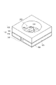
- FIG. 1 is a perspective view showing one embodiment of a substrate for mounting an optical semiconductor element.
- the optical semiconductor element mounting substrate of FIG. 1 includes a substrate, and first connection terminals and second connection terminals provided on the substrate, and the first connection terminals and the second connection terminals are connected to each other. It has a cured product of the light-reflecting thermosetting resin composition of the present embodiment between them. More specifically, the optical semiconductor element mounting substrate 110 includes metal wiring 105 (first connection terminal and second connection terminal) on which Ni/Ag plating 104 is formed, and metal wiring 105 (first connection terminal). and a reflector 103, the metal wiring 105 formed with Ni/Ag plating 104, the insulating resin molded body 103' and the reflector.
- the bottom surface of the concave portion 200 is composed of the metal wiring 105 with the Ni/Ag plating 104 formed thereon and the insulating resin molding 103 ′, and the wall surface of the concave portion 200 is composed of the reflector 103 .
- the reflector 103 and the insulating resin molded body 103' are molded bodies made of the cured thermosetting resin composition for light reflection according to the present embodiment.
- FIG. 2 is a schematic diagram showing an embodiment of a process for manufacturing a substrate for mounting an optical semiconductor element.
- the substrate for mounting an optical semiconductor element is formed by, for example, punching out from a metal foil, forming metal wiring 105 by a known method such as etching, applying Ni/Ag plating 104 by electroplating (FIG. 2(a)), and then a step of placing the metal wiring 105 in a mold 151 having a predetermined shape, injecting a thermosetting resin composition for light reflection from a resin injection port 150 of the mold 151, and performing transfer molding under predetermined conditions (see FIG.
- an optical semiconductor element mounting region (recess) 200 surrounded by a reflector 103 made of a cured product of a light reflecting thermosetting resin composition is formed on the optical semiconductor element mounting substrate.
- the bottom surface of the concave portion 200 is composed of the metal wiring 105 serving as the first connection terminal, the metal wiring 105 serving as the second connection terminal, and the cured product of the light-reflecting thermosetting resin composition provided between them. and an insulating resin molded body 103'.
- the transfer molding conditions are as follows: mold temperature is preferably 170 to 200° C., more preferably 170 to 190° C.; molding pressure is preferably 0.5 to 20 MPa, more preferably 2 to 8 MPa; 120 seconds, 1 to 3 hours at an after cure temperature of 120° C. to 180° C. are preferable.
- An optical semiconductor device includes the optical semiconductor element mounting substrate and an optical semiconductor element mounted on the optical semiconductor element mounting substrate.
- the substrate for mounting an optical semiconductor element the optical semiconductor element provided in the concave portion of the substrate for mounting an optical semiconductor element, and the phosphor-containing encapsulant that fills the concave portion to seal the optical semiconductor element.
- an optical semiconductor device including a stopping resin portion the substrate for mounting an optical semiconductor element, the optical semiconductor element provided in the concave portion of the substrate for mounting an optical semiconductor element, and the phosphor-containing encapsulant that fills the concave portion to seal the optical semiconductor element.
- FIG. 3 is a perspective view showing an embodiment in which the optical semiconductor element 100 is mounted on the substrate 110 for mounting an optical semiconductor element.
- the optical semiconductor element 100 is mounted at a predetermined position in an optical semiconductor element mounting region (concave portion) 200 of an optical semiconductor element mounting substrate 110, and is electrically connected to a metal wiring 105 and a bonding wire 102.
- 4 and 5 are schematic cross-sectional views showing an embodiment of the optical semiconductor device.
- the optical semiconductor device includes an optical semiconductor element mounting substrate 110, an optical semiconductor element 100 provided at a predetermined position in a recess 200 of the optical semiconductor element mounting substrate 110, and a recess 200.
- 105 are electrically connected by bonding wires 102 or solder bumps 107 .
- FIG. 6 is also a schematic cross-sectional view showing one embodiment of the optical semiconductor device.
- the LED element 300 is arranged at a predetermined position on the lead 304 on which the reflector 303 is formed via the die bonding material 306, and the LED element 300 and the lead 304 are electrically connected by the bonding wire 301.
- the LED element 300 is sealed with a transparent sealing resin 302 that is connected and contains a phosphor 305 .
- the light-reflecting thermosetting resin composition of the present embodiment can be used, for example, as a light-reflecting coating agent for copper-clad laminates, substrates for mounting optical semiconductor elements, optical semiconductor elements, and the like.
- a copper-clad laminate according to the present embodiment includes a light-reflecting resin layer formed using the light-reflecting thermosetting resin composition described above, and a copper foil laminated on the light-reflecting resin layer. .
- FIG. 7 is a schematic cross-sectional view showing a preferred embodiment of a copper-clad laminate.
- a copper clad laminate 400 includes a base material 401, a light reflecting resin layer 402 laminated on the base material 401, and a copper foil 403 laminated on the light reflecting resin layer 402. , is equipped with
- the light reflecting resin layer 402 is formed using the light reflecting thermosetting resin composition described above.
- a base material used for a copper-clad laminate can be used without particular limitation, and examples thereof include a resin laminate such as an epoxy resin laminate and a substrate for mounting an optical semiconductor.
- the copper-clad laminate 400 is produced, for example, by applying the light-reflecting thermosetting resin composition of the present embodiment to the surface of the substrate 401, overlaying the copper foil 403, and heating and pressurizing to cure the thermosetting resin composition.
- thermosetting resin composition As a method for applying the thermosetting resin composition to the substrate 401, for example, a printing method, a die coating method, a curtain coating method, a spray coating method, a roll coating method, or the like can be used.
- the thermosetting resin composition may contain a solvent so as to facilitate application.
- a solvent it is preferable to set the total amount excluding the solvent when the total amount of the thermosetting resin composition is based on the mixing ratio of each component described above.
- the conditions for heating and pressurization are not particularly limited, but for example, it is preferable to perform heating and pressurization under conditions of 130 to 180° C., 0.5 to 4 MPa, and 30 to 600 minutes.
- the reflective resin layer 402 and the copper foil 403 may be laminated respectively.
- the copper-clad laminate may be composed only of the light reflecting resin layer 402 and the copper foil 403 without using the base material 401 .
- the light reflecting resin layer 402 will play a role as a base material.
- the light reflecting resin layer 402 can be obtained by impregnating a glass cloth or the like with the present thermosetting resin composition and curing the composition.
- FIG. 8 is a schematic cross-sectional view showing an example of an optical semiconductor device produced using a copper-clad laminate.
- the optical semiconductor device 500 is a surface-mounted light-emitting diode that includes an optical semiconductor element 410 and a transparent sealing resin 404 provided to seal the optical semiconductor element 410.
- optical semiconductor element 410 is adhered to copper foil 403 via adhesive layer 408 and electrically connected to copper foil 403 by bonding wire 409 .
- a substrate for mounting an optical semiconductor element As another embodiment of a substrate for mounting an optical semiconductor element, a light-reflecting resin layer formed between a plurality of conductor members (connection terminals) on a substrate using the above-described light-reflecting thermosetting resin composition.
- An optical semiconductor element mounting substrate provided with the optical semiconductor element may be mentioned.
- Another embodiment of an optical semiconductor device is obtained by mounting an optical semiconductor element on the above substrate for mounting an optical semiconductor element.
- FIG. 9 is a schematic cross-sectional view showing a preferred embodiment of an optical semiconductor device.
- an optical semiconductor device 600 includes a substrate 601, a plurality of conductor members 602 formed on the surface of the substrate 601, and a plurality of conductor members (connection terminals) formed between the 602,
- An optical semiconductor element 610 is mounted on an optical semiconductor element mounting substrate provided with a light reflecting resin layer 603 containing a cured product of the thermosetting resin composition for light reflection, and the optical semiconductor element 610 is sealed. It is a surface-mounted light-emitting diode in which a transparent sealing resin 604 is provided on the surface.
- optical semiconductor element 610 is adhered to conductor member 602 via adhesive layer 608 and electrically connected to conductor member 602 by bonding wire 609 .
- a base material used for a substrate for mounting an optical semiconductor element can be used without particular limitation, and examples thereof include resin laminates such as epoxy resin laminates.
- the conductor member 602 functions as a connection terminal, and can be formed by a known method such as photoetching a copper foil.
- the substrate for mounting an optical semiconductor element is obtained by applying the light reflecting thermosetting resin composition between the plurality of conductor members 602 on the base material 601 and heating and curing to obtain a cured product of the light reflecting thermosetting resin composition.
- thermosetting resin composition for light reflection may contain a solvent so as to facilitate application.
- a solvent it is preferable to set the total amount of the resin composition excluding the solvent when the mixing ratio of each component described above is based on the total amount of the resin composition.
- the heating conditions for heat-curing the coating film of the thermosetting resin composition for light reflection are not particularly limited.
- the conductor member 602 may be subjected to roughening treatment such as oxidation-reduction treatment, CZ treatment (manufactured by MEC Co., Ltd.).
- the substrate for mounting an optical semiconductor element and the optical semiconductor device having the cured product of the thermosetting resin composition for light reflection according to the present embodiment have high light reflectance, and even when used at high temperatures for a long time, the optical properties are maintained. can be maintained.
- thermosetting resin composition for light reflection In order to prepare the light-reflecting thermosetting resin compositions of Examples and Comparative Examples, the following components were prepared.
- thermosetting resin composition for light reflection.
- the light-reflecting thermosetting resin composition was transfer-molded under conditions of a mold temperature of 180°C, a molding pressure of 6.9 MPa, and a curing time of 90 seconds, and then post-cured at 150°C for 2 hours to obtain a thickness of 3.
- a 0 mm test piece was produced.
- CM-600d manufactured by Konica Minolta, Inc.
- the light reflectance of the test piece at a wavelength of 460 nm was measured.
- the light reflectance was measured after the test piece was allowed to stand in a constant temperature bath set at 150° C. for 1008 hours.
- b value The b value was calculated using a spectrophotometer "CM-600d" for the test piece prepared by the above light reflectance measurement.
- the light-reflecting thermosetting resin compositions of Examples are capable of forming cured products (molded products) having high initial light reflectance and excellent light reflectivity even when used at high temperatures for a long time. can be confirmed.
- SYMBOLS 100 Optical-semiconductor element, 101... Encapsulation resin, 102... Bonding wire, 103... Reflector, 103'... Insulating resin molding, 104... Ni/Ag plating, 105... Metal wiring, 106... Phosphor, 107... Solder Bump 110 Optical semiconductor element mounting substrate 150 Resin injection port 151 Mold 200 Optical semiconductor element mounting area 300 LED element 301 Bonding wire 302 Sealing resin 303 Reflector DESCRIPTION OF SYMBOLS 304... Lead, 305... Phosphor, 306... Die-bonding material, 400... Copper-clad laminate, 401... Base material, 402... Light reflecting resin layer, 403... Copper foil, 404...
- Sealing resin 408... Adhesive layer, 409 ... Bonding wire 410 ... Optical semiconductor element 500, 600 ... Optical semiconductor device 601 ... Base material 602 ... Conductor member 603 ... Light reflecting resin layer 604 . Sealing resin 608 ... Adhesive layer 609 ... Bonding wire , 610 . . . optical semiconductor elements.
Landscapes
- Chemical & Material Sciences (AREA)
- Health & Medical Sciences (AREA)
- Chemical Kinetics & Catalysis (AREA)
- Medicinal Chemistry (AREA)
- Polymers & Plastics (AREA)
- Organic Chemistry (AREA)
- Engineering & Computer Science (AREA)
- Microelectronics & Electronic Packaging (AREA)
- Manufacturing & Machinery (AREA)
- Computer Hardware Design (AREA)
- Power Engineering (AREA)
- Led Device Packages (AREA)
- Compositions Of Macromolecular Compounds (AREA)
Abstract
Un aspect de la présente invention concerne une composition de résine thermodurcissable pour la réflexion de la lumière qui comprend une résine époxyde, un durcisseur, un composé benzoxazole ayant une intensité fluorescente à 410-500 nm, des particules creuses inorganiques et un pigment blanc.
Priority Applications (3)
| Application Number | Priority Date | Filing Date | Title |
|---|---|---|---|
| KR1020237039025A KR20240031218A (ko) | 2021-07-05 | 2022-05-17 | 광반사용 열경화성 수지 조성물, 광반도체 소자 탑재용 기판 및 광반도체 장치 |
| JP2023533457A JPWO2023281922A1 (fr) | 2021-07-05 | 2022-05-17 | |
| CN202280035085.XA CN117425696A (zh) | 2021-07-05 | 2022-05-17 | 光反射用热固性树脂组合物、光半导体元件搭载用基板及光半导体装置 |
Applications Claiming Priority (2)
| Application Number | Priority Date | Filing Date | Title |
|---|---|---|---|
| JP2021111370 | 2021-07-05 | ||
| JP2021-111370 | 2021-07-05 |
Publications (1)
| Publication Number | Publication Date |
|---|---|
| WO2023281922A1 true WO2023281922A1 (fr) | 2023-01-12 |
Family
ID=84800540
Family Applications (1)
| Application Number | Title | Priority Date | Filing Date |
|---|---|---|---|
| PCT/JP2022/020531 WO2023281922A1 (fr) | 2021-07-05 | 2022-05-17 | Composition de résine thermodurcissable pour réflexion de lumière, substrat pour le montage d'un élément semi-conducteur optique, et dispositif semi-conducteur optique |
Country Status (5)
| Country | Link |
|---|---|
| JP (1) | JPWO2023281922A1 (fr) |
| KR (1) | KR20240031218A (fr) |
| CN (1) | CN117425696A (fr) |
| TW (1) | TW202307059A (fr) |
| WO (1) | WO2023281922A1 (fr) |
Citations (5)
| Publication number | Priority date | Publication date | Assignee | Title |
|---|---|---|---|---|
| JP2014221856A (ja) * | 2013-05-13 | 2014-11-27 | パナソニック株式会社 | 光反射体用熱硬化性樹脂組成物 |
| JP2015152643A (ja) * | 2014-02-10 | 2015-08-24 | パナソニックIpマネジメント株式会社 | 光反射体用熱硬化性樹脂組成物、光反射体、及び発光装置 |
| JP2017020026A (ja) * | 2006-11-15 | 2017-01-26 | 日立化成株式会社 | 熱硬化性光反射用樹脂組成物、並びにその樹脂組成物を用いた光半導体素子搭載用基板及び光半導体装置 |
| JP6417320B2 (ja) * | 2012-05-16 | 2018-11-07 | ボレアリス アーゲーBorealis Ag | ポリマーシート |
| JP2019108457A (ja) * | 2017-12-18 | 2019-07-04 | 日立化成株式会社 | 光反射用熱硬化性樹脂タブレット、光半導体素子搭載用基板及びその製造方法、並びに光半導体装置 |
Family Cites Families (1)
| Publication number | Priority date | Publication date | Assignee | Title |
|---|---|---|---|---|
| JP5665285B2 (ja) | 2009-06-15 | 2015-02-04 | 日立化成株式会社 | 光半導体素子搭載用部材及び光半導体装置 |
-
2022
- 2022-05-17 CN CN202280035085.XA patent/CN117425696A/zh active Pending
- 2022-05-17 JP JP2023533457A patent/JPWO2023281922A1/ja active Pending
- 2022-05-17 KR KR1020237039025A patent/KR20240031218A/ko unknown
- 2022-05-17 WO PCT/JP2022/020531 patent/WO2023281922A1/fr active Application Filing
- 2022-06-01 TW TW111120363A patent/TW202307059A/zh unknown
Patent Citations (5)
| Publication number | Priority date | Publication date | Assignee | Title |
|---|---|---|---|---|
| JP2017020026A (ja) * | 2006-11-15 | 2017-01-26 | 日立化成株式会社 | 熱硬化性光反射用樹脂組成物、並びにその樹脂組成物を用いた光半導体素子搭載用基板及び光半導体装置 |
| JP6417320B2 (ja) * | 2012-05-16 | 2018-11-07 | ボレアリス アーゲーBorealis Ag | ポリマーシート |
| JP2014221856A (ja) * | 2013-05-13 | 2014-11-27 | パナソニック株式会社 | 光反射体用熱硬化性樹脂組成物 |
| JP2015152643A (ja) * | 2014-02-10 | 2015-08-24 | パナソニックIpマネジメント株式会社 | 光反射体用熱硬化性樹脂組成物、光反射体、及び発光装置 |
| JP2019108457A (ja) * | 2017-12-18 | 2019-07-04 | 日立化成株式会社 | 光反射用熱硬化性樹脂タブレット、光半導体素子搭載用基板及びその製造方法、並びに光半導体装置 |
Also Published As
| Publication number | Publication date |
|---|---|
| TW202307059A (zh) | 2023-02-16 |
| KR20240031218A (ko) | 2024-03-07 |
| JPWO2023281922A1 (fr) | 2023-01-12 |
| CN117425696A (zh) | 2024-01-19 |
Similar Documents
| Publication | Publication Date | Title |
|---|---|---|
| JP5298468B2 (ja) | 熱硬化性光反射用樹脂組成物、これを用いた光半導体素子搭載用基板とその製造方法および光半導体装置 | |
| JP5303097B2 (ja) | 熱硬化性光反射用樹脂組成物、ならびにこれを用いた光半導体搭載用基板とその製造方法および光半導体装置。 | |
| JP5665285B2 (ja) | 光半導体素子搭載用部材及び光半導体装置 | |
| JP2007297601A (ja) | 光反射用熱硬化性樹脂組成物、これを用いた光半導体素子搭載用基板とその製造方法および光半導体装置 | |
| JP2006140207A (ja) | 光反射用熱硬化性樹脂組成物、ならびにこれを用いた光半導体搭載用基板とその製造方法および光半導体装置。 | |
| JP2010235756A (ja) | 光反射用熱硬化性樹脂組成物、これを用いた光半導体素子搭載用基板及びその製造方法、並びに光半導体装置 | |
| JP2008306151A (ja) | 光半導体用エポキシ樹脂組成物、ならびにこれを用いた光半導体素子搭載用基板および光半導体装置 | |
| JP5233186B2 (ja) | 熱硬化性光反射用樹脂組成物、これを用いた光半導体素子搭載用基板とその製造方法および光半導体装置 | |
| JP2022075700A (ja) | 光反射用熱硬化性樹脂組成物、光半導体素子搭載用基板及びその製造方法、並びに光半導体装置 | |
| JP5760379B2 (ja) | 光半導体装置の製造方法及び光半導体装置 | |
| JP6133004B2 (ja) | 光反射用熱硬化性樹脂組成物、光半導体素子搭載用基板及びその製造方法、並びに光半導体装置 | |
| JP5936804B2 (ja) | 熱硬化性樹脂組成物、光半導体素子搭載用基板及びその製造方法、並びに光半導体装置 | |
| WO2023281922A1 (fr) | Composition de résine thermodurcissable pour réflexion de lumière, substrat pour le montage d'un élément semi-conducteur optique, et dispositif semi-conducteur optique | |
| JP7459878B2 (ja) | 光反射用熱硬化性樹脂組成物、光半導体素子搭載用基板及び光半導体装置 | |
| JP5967135B2 (ja) | 熱硬化性光反射用樹脂組成物、ならびにこれを用いた光半導体搭載用基板とその製造方法および光半導体装置。 | |
| WO2021038771A1 (fr) | Composition de résine thermodurcissable pour réflexion optique, substrat pour le montage d'un élément semi-conducteur optique, et dispositif semi-conducteur optique | |
| JP7294429B2 (ja) | 光反射用熱硬化性樹脂組成物、光半導体素子搭載用基板及び光半導体装置 | |
| JP6988234B2 (ja) | 光反射用熱硬化性樹脂組成物、光半導体素子搭載用基板及びその製造方法、並びに光半導体装置 | |
| JP6191705B2 (ja) | 光反射用熱硬化性樹脂組成物、光半導体素子搭載用基板及びその製造方法、並びに光半導体装置 | |
| JP2022053019A (ja) | 光反射用熱硬化性樹脂組成物、光半導体素子搭載用基板及び光半導体装置 | |
| JP6209928B2 (ja) | 光半導体装置、光半導体素子搭載用基板及び光反射用熱硬化性樹脂組成物 | |
| JP5831424B2 (ja) | 光反射用熱硬化性樹脂組成物、光半導体素子搭載用基板及びその製造方法、並びに光半導体装置 | |
| JP6337996B2 (ja) | 光反射用熱硬化性樹脂組成物、光半導体素子搭載用基板及びその製造方法、並びに光半導体装置 | |
| JP2013168684A (ja) | 光半導体素子搭載用部材及び光半導体装置 | |
| JP2012178567A (ja) | 光反射用熱硬化性樹脂組成物、これを用いた光半導体素子搭載用基板とその製造方法および光半導体装置 |
Legal Events
| Date | Code | Title | Description |
|---|---|---|---|
| 121 | Ep: the epo has been informed by wipo that ep was designated in this application |
Ref document number: 22837343 Country of ref document: EP Kind code of ref document: A1 |
|
| WWE | Wipo information: entry into national phase |
Ref document number: 2023533457 Country of ref document: JP |
|
| WWE | Wipo information: entry into national phase |
Ref document number: 202280035085.X Country of ref document: CN |
|
| NENP | Non-entry into the national phase |
Ref country code: DE |