WO2023276066A1 - 切削工具 - Google Patents
切削工具 Download PDFInfo
- Publication number
- WO2023276066A1 WO2023276066A1 PCT/JP2021/024828 JP2021024828W WO2023276066A1 WO 2023276066 A1 WO2023276066 A1 WO 2023276066A1 JP 2021024828 W JP2021024828 W JP 2021024828W WO 2023276066 A1 WO2023276066 A1 WO 2023276066A1
- Authority
- WO
- WIPO (PCT)
- Prior art keywords
- layer
- less
- sample
- coating
- unit
- Prior art date
- Legal status (The legal status is an assumption and is not a legal conclusion. Google has not performed a legal analysis and makes no representation as to the accuracy of the status listed.)
- Ceased
Links
Images




Classifications
-
- B—PERFORMING OPERATIONS; TRANSPORTING
- B23—MACHINE TOOLS; METAL-WORKING NOT OTHERWISE PROVIDED FOR
- B23B—TURNING; BORING
- B23B27/00—Tools for turning or boring machines; Tools of a similar kind in general; Accessories therefor
- B23B27/14—Cutting tools of which the bits or tips or cutting inserts are of special material
- B23B27/148—Composition of the cutting inserts
-
- C—CHEMISTRY; METALLURGY
- C23—COATING METALLIC MATERIAL; COATING MATERIAL WITH METALLIC MATERIAL; CHEMICAL SURFACE TREATMENT; DIFFUSION TREATMENT OF METALLIC MATERIAL; COATING BY VACUUM EVAPORATION, BY SPUTTERING, BY ION IMPLANTATION OR BY CHEMICAL VAPOUR DEPOSITION, IN GENERAL; INHIBITING CORROSION OF METALLIC MATERIAL OR INCRUSTATION IN GENERAL
- C23C—COATING METALLIC MATERIAL; COATING MATERIAL WITH METALLIC MATERIAL; SURFACE TREATMENT OF METALLIC MATERIAL BY DIFFUSION INTO THE SURFACE, BY CHEMICAL CONVERSION OR SUBSTITUTION; COATING BY VACUUM EVAPORATION, BY SPUTTERING, BY ION IMPLANTATION OR BY CHEMICAL VAPOUR DEPOSITION, IN GENERAL
- C23C30/00—Coating with metallic material characterised only by the composition of the metallic material, i.e. not characterised by the coating process
- C23C30/005—Coating with metallic material characterised only by the composition of the metallic material, i.e. not characterised by the coating process on hard metal substrates
-
- B—PERFORMING OPERATIONS; TRANSPORTING
- B23—MACHINE TOOLS; METAL-WORKING NOT OTHERWISE PROVIDED FOR
- B23B—TURNING; BORING
- B23B27/00—Tools for turning or boring machines; Tools of a similar kind in general; Accessories therefor
- B23B27/14—Cutting tools of which the bits or tips or cutting inserts are of special material
-
- C—CHEMISTRY; METALLURGY
- C23—COATING METALLIC MATERIAL; COATING MATERIAL WITH METALLIC MATERIAL; CHEMICAL SURFACE TREATMENT; DIFFUSION TREATMENT OF METALLIC MATERIAL; COATING BY VACUUM EVAPORATION, BY SPUTTERING, BY ION IMPLANTATION OR BY CHEMICAL VAPOUR DEPOSITION, IN GENERAL; INHIBITING CORROSION OF METALLIC MATERIAL OR INCRUSTATION IN GENERAL
- C23C—COATING METALLIC MATERIAL; COATING MATERIAL WITH METALLIC MATERIAL; SURFACE TREATMENT OF METALLIC MATERIAL BY DIFFUSION INTO THE SURFACE, BY CHEMICAL CONVERSION OR SUBSTITUTION; COATING BY VACUUM EVAPORATION, BY SPUTTERING, BY ION IMPLANTATION OR BY CHEMICAL VAPOUR DEPOSITION, IN GENERAL
- C23C14/00—Coating by vacuum evaporation, by sputtering or by ion implantation of the coating forming material
- C23C14/06—Coating by vacuum evaporation, by sputtering or by ion implantation of the coating forming material characterised by the coating material
-
- C—CHEMISTRY; METALLURGY
- C23—COATING METALLIC MATERIAL; COATING MATERIAL WITH METALLIC MATERIAL; CHEMICAL SURFACE TREATMENT; DIFFUSION TREATMENT OF METALLIC MATERIAL; COATING BY VACUUM EVAPORATION, BY SPUTTERING, BY ION IMPLANTATION OR BY CHEMICAL VAPOUR DEPOSITION, IN GENERAL; INHIBITING CORROSION OF METALLIC MATERIAL OR INCRUSTATION IN GENERAL
- C23C—COATING METALLIC MATERIAL; COATING MATERIAL WITH METALLIC MATERIAL; SURFACE TREATMENT OF METALLIC MATERIAL BY DIFFUSION INTO THE SURFACE, BY CHEMICAL CONVERSION OR SUBSTITUTION; COATING BY VACUUM EVAPORATION, BY SPUTTERING, BY ION IMPLANTATION OR BY CHEMICAL VAPOUR DEPOSITION, IN GENERAL
- C23C14/00—Coating by vacuum evaporation, by sputtering or by ion implantation of the coating forming material
- C23C14/06—Coating by vacuum evaporation, by sputtering or by ion implantation of the coating forming material characterised by the coating material
- C23C14/0635—Carbides
-
- C—CHEMISTRY; METALLURGY
- C23—COATING METALLIC MATERIAL; COATING MATERIAL WITH METALLIC MATERIAL; CHEMICAL SURFACE TREATMENT; DIFFUSION TREATMENT OF METALLIC MATERIAL; COATING BY VACUUM EVAPORATION, BY SPUTTERING, BY ION IMPLANTATION OR BY CHEMICAL VAPOUR DEPOSITION, IN GENERAL; INHIBITING CORROSION OF METALLIC MATERIAL OR INCRUSTATION IN GENERAL
- C23C—COATING METALLIC MATERIAL; COATING MATERIAL WITH METALLIC MATERIAL; SURFACE TREATMENT OF METALLIC MATERIAL BY DIFFUSION INTO THE SURFACE, BY CHEMICAL CONVERSION OR SUBSTITUTION; COATING BY VACUUM EVAPORATION, BY SPUTTERING, BY ION IMPLANTATION OR BY CHEMICAL VAPOUR DEPOSITION, IN GENERAL
- C23C14/00—Coating by vacuum evaporation, by sputtering or by ion implantation of the coating forming material
- C23C14/06—Coating by vacuum evaporation, by sputtering or by ion implantation of the coating forming material characterised by the coating material
- C23C14/0641—Nitrides
-
- C—CHEMISTRY; METALLURGY
- C23—COATING METALLIC MATERIAL; COATING MATERIAL WITH METALLIC MATERIAL; CHEMICAL SURFACE TREATMENT; DIFFUSION TREATMENT OF METALLIC MATERIAL; COATING BY VACUUM EVAPORATION, BY SPUTTERING, BY ION IMPLANTATION OR BY CHEMICAL VAPOUR DEPOSITION, IN GENERAL; INHIBITING CORROSION OF METALLIC MATERIAL OR INCRUSTATION IN GENERAL
- C23C—COATING METALLIC MATERIAL; COATING MATERIAL WITH METALLIC MATERIAL; SURFACE TREATMENT OF METALLIC MATERIAL BY DIFFUSION INTO THE SURFACE, BY CHEMICAL CONVERSION OR SUBSTITUTION; COATING BY VACUUM EVAPORATION, BY SPUTTERING, BY ION IMPLANTATION OR BY CHEMICAL VAPOUR DEPOSITION, IN GENERAL
- C23C14/00—Coating by vacuum evaporation, by sputtering or by ion implantation of the coating forming material
- C23C14/06—Coating by vacuum evaporation, by sputtering or by ion implantation of the coating forming material characterised by the coating material
- C23C14/0641—Nitrides
- C23C14/0647—Boron nitride
-
- C—CHEMISTRY; METALLURGY
- C23—COATING METALLIC MATERIAL; COATING MATERIAL WITH METALLIC MATERIAL; CHEMICAL SURFACE TREATMENT; DIFFUSION TREATMENT OF METALLIC MATERIAL; COATING BY VACUUM EVAPORATION, BY SPUTTERING, BY ION IMPLANTATION OR BY CHEMICAL VAPOUR DEPOSITION, IN GENERAL; INHIBITING CORROSION OF METALLIC MATERIAL OR INCRUSTATION IN GENERAL
- C23C—COATING METALLIC MATERIAL; COATING MATERIAL WITH METALLIC MATERIAL; SURFACE TREATMENT OF METALLIC MATERIAL BY DIFFUSION INTO THE SURFACE, BY CHEMICAL CONVERSION OR SUBSTITUTION; COATING BY VACUUM EVAPORATION, BY SPUTTERING, BY ION IMPLANTATION OR BY CHEMICAL VAPOUR DEPOSITION, IN GENERAL
- C23C14/00—Coating by vacuum evaporation, by sputtering or by ion implantation of the coating forming material
- C23C14/06—Coating by vacuum evaporation, by sputtering or by ion implantation of the coating forming material characterised by the coating material
- C23C14/0641—Nitrides
- C23C14/0652—Silicon nitride
-
- C—CHEMISTRY; METALLURGY
- C23—COATING METALLIC MATERIAL; COATING MATERIAL WITH METALLIC MATERIAL; CHEMICAL SURFACE TREATMENT; DIFFUSION TREATMENT OF METALLIC MATERIAL; COATING BY VACUUM EVAPORATION, BY SPUTTERING, BY ION IMPLANTATION OR BY CHEMICAL VAPOUR DEPOSITION, IN GENERAL; INHIBITING CORROSION OF METALLIC MATERIAL OR INCRUSTATION IN GENERAL
- C23C—COATING METALLIC MATERIAL; COATING MATERIAL WITH METALLIC MATERIAL; SURFACE TREATMENT OF METALLIC MATERIAL BY DIFFUSION INTO THE SURFACE, BY CHEMICAL CONVERSION OR SUBSTITUTION; COATING BY VACUUM EVAPORATION, BY SPUTTERING, BY ION IMPLANTATION OR BY CHEMICAL VAPOUR DEPOSITION, IN GENERAL
- C23C14/00—Coating by vacuum evaporation, by sputtering or by ion implantation of the coating forming material
- C23C14/22—Coating by vacuum evaporation, by sputtering or by ion implantation of the coating forming material characterised by the process of coating
- C23C14/24—Vacuum evaporation
- C23C14/28—Vacuum evaporation by wave energy or particle radiation
- C23C14/30—Vacuum evaporation by wave energy or particle radiation by electron bombardment
-
- C—CHEMISTRY; METALLURGY
- C23—COATING METALLIC MATERIAL; COATING MATERIAL WITH METALLIC MATERIAL; CHEMICAL SURFACE TREATMENT; DIFFUSION TREATMENT OF METALLIC MATERIAL; COATING BY VACUUM EVAPORATION, BY SPUTTERING, BY ION IMPLANTATION OR BY CHEMICAL VAPOUR DEPOSITION, IN GENERAL; INHIBITING CORROSION OF METALLIC MATERIAL OR INCRUSTATION IN GENERAL
- C23C—COATING METALLIC MATERIAL; COATING MATERIAL WITH METALLIC MATERIAL; SURFACE TREATMENT OF METALLIC MATERIAL BY DIFFUSION INTO THE SURFACE, BY CHEMICAL CONVERSION OR SUBSTITUTION; COATING BY VACUUM EVAPORATION, BY SPUTTERING, BY ION IMPLANTATION OR BY CHEMICAL VAPOUR DEPOSITION, IN GENERAL
- C23C14/00—Coating by vacuum evaporation, by sputtering or by ion implantation of the coating forming material
- C23C14/22—Coating by vacuum evaporation, by sputtering or by ion implantation of the coating forming material characterised by the process of coating
- C23C14/24—Vacuum evaporation
- C23C14/32—Vacuum evaporation by explosion; by evaporation and subsequent ionisation of the vapours, e.g. ion-plating
-
- C—CHEMISTRY; METALLURGY
- C23—COATING METALLIC MATERIAL; COATING MATERIAL WITH METALLIC MATERIAL; CHEMICAL SURFACE TREATMENT; DIFFUSION TREATMENT OF METALLIC MATERIAL; COATING BY VACUUM EVAPORATION, BY SPUTTERING, BY ION IMPLANTATION OR BY CHEMICAL VAPOUR DEPOSITION, IN GENERAL; INHIBITING CORROSION OF METALLIC MATERIAL OR INCRUSTATION IN GENERAL
- C23C—COATING METALLIC MATERIAL; COATING MATERIAL WITH METALLIC MATERIAL; SURFACE TREATMENT OF METALLIC MATERIAL BY DIFFUSION INTO THE SURFACE, BY CHEMICAL CONVERSION OR SUBSTITUTION; COATING BY VACUUM EVAPORATION, BY SPUTTERING, BY ION IMPLANTATION OR BY CHEMICAL VAPOUR DEPOSITION, IN GENERAL
- C23C28/00—Coating for obtaining at least two superposed coatings either by methods not provided for in a single one of groups C23C2/00 - C23C26/00 or by combinations of methods provided for in subclasses C23C and C25C or C25D
- C23C28/04—Coating for obtaining at least two superposed coatings either by methods not provided for in a single one of groups C23C2/00 - C23C26/00 or by combinations of methods provided for in subclasses C23C and C25C or C25D only coatings of inorganic non-metallic material
-
- C—CHEMISTRY; METALLURGY
- C23—COATING METALLIC MATERIAL; COATING MATERIAL WITH METALLIC MATERIAL; CHEMICAL SURFACE TREATMENT; DIFFUSION TREATMENT OF METALLIC MATERIAL; COATING BY VACUUM EVAPORATION, BY SPUTTERING, BY ION IMPLANTATION OR BY CHEMICAL VAPOUR DEPOSITION, IN GENERAL; INHIBITING CORROSION OF METALLIC MATERIAL OR INCRUSTATION IN GENERAL
- C23C—COATING METALLIC MATERIAL; COATING MATERIAL WITH METALLIC MATERIAL; SURFACE TREATMENT OF METALLIC MATERIAL BY DIFFUSION INTO THE SURFACE, BY CHEMICAL CONVERSION OR SUBSTITUTION; COATING BY VACUUM EVAPORATION, BY SPUTTERING, BY ION IMPLANTATION OR BY CHEMICAL VAPOUR DEPOSITION, IN GENERAL
- C23C28/00—Coating for obtaining at least two superposed coatings either by methods not provided for in a single one of groups C23C2/00 - C23C26/00 or by combinations of methods provided for in subclasses C23C and C25C or C25D
- C23C28/04—Coating for obtaining at least two superposed coatings either by methods not provided for in a single one of groups C23C2/00 - C23C26/00 or by combinations of methods provided for in subclasses C23C and C25C or C25D only coatings of inorganic non-metallic material
- C23C28/044—Coating for obtaining at least two superposed coatings either by methods not provided for in a single one of groups C23C2/00 - C23C26/00 or by combinations of methods provided for in subclasses C23C and C25C or C25D only coatings of inorganic non-metallic material coatings specially adapted for cutting tools or wear applications
-
- C—CHEMISTRY; METALLURGY
- C23—COATING METALLIC MATERIAL; COATING MATERIAL WITH METALLIC MATERIAL; CHEMICAL SURFACE TREATMENT; DIFFUSION TREATMENT OF METALLIC MATERIAL; COATING BY VACUUM EVAPORATION, BY SPUTTERING, BY ION IMPLANTATION OR BY CHEMICAL VAPOUR DEPOSITION, IN GENERAL; INHIBITING CORROSION OF METALLIC MATERIAL OR INCRUSTATION IN GENERAL
- C23C—COATING METALLIC MATERIAL; COATING MATERIAL WITH METALLIC MATERIAL; SURFACE TREATMENT OF METALLIC MATERIAL BY DIFFUSION INTO THE SURFACE, BY CHEMICAL CONVERSION OR SUBSTITUTION; COATING BY VACUUM EVAPORATION, BY SPUTTERING, BY ION IMPLANTATION OR BY CHEMICAL VAPOUR DEPOSITION, IN GENERAL
- C23C28/00—Coating for obtaining at least two superposed coatings either by methods not provided for in a single one of groups C23C2/00 - C23C26/00 or by combinations of methods provided for in subclasses C23C and C25C or C25D
- C23C28/40—Coatings including alternating layers following a pattern, a periodic or defined repetition
-
- C—CHEMISTRY; METALLURGY
- C23—COATING METALLIC MATERIAL; COATING MATERIAL WITH METALLIC MATERIAL; CHEMICAL SURFACE TREATMENT; DIFFUSION TREATMENT OF METALLIC MATERIAL; COATING BY VACUUM EVAPORATION, BY SPUTTERING, BY ION IMPLANTATION OR BY CHEMICAL VAPOUR DEPOSITION, IN GENERAL; INHIBITING CORROSION OF METALLIC MATERIAL OR INCRUSTATION IN GENERAL
- C23C—COATING METALLIC MATERIAL; COATING MATERIAL WITH METALLIC MATERIAL; SURFACE TREATMENT OF METALLIC MATERIAL BY DIFFUSION INTO THE SURFACE, BY CHEMICAL CONVERSION OR SUBSTITUTION; COATING BY VACUUM EVAPORATION, BY SPUTTERING, BY ION IMPLANTATION OR BY CHEMICAL VAPOUR DEPOSITION, IN GENERAL
- C23C28/00—Coating for obtaining at least two superposed coatings either by methods not provided for in a single one of groups C23C2/00 - C23C26/00 or by combinations of methods provided for in subclasses C23C and C25C or C25D
- C23C28/40—Coatings including alternating layers following a pattern, a periodic or defined repetition
- C23C28/42—Coatings including alternating layers following a pattern, a periodic or defined repetition characterized by the composition of the alternating layers
-
- C—CHEMISTRY; METALLURGY
- C23—COATING METALLIC MATERIAL; COATING MATERIAL WITH METALLIC MATERIAL; CHEMICAL SURFACE TREATMENT; DIFFUSION TREATMENT OF METALLIC MATERIAL; COATING BY VACUUM EVAPORATION, BY SPUTTERING, BY ION IMPLANTATION OR BY CHEMICAL VAPOUR DEPOSITION, IN GENERAL; INHIBITING CORROSION OF METALLIC MATERIAL OR INCRUSTATION IN GENERAL
- C23C—COATING METALLIC MATERIAL; COATING MATERIAL WITH METALLIC MATERIAL; SURFACE TREATMENT OF METALLIC MATERIAL BY DIFFUSION INTO THE SURFACE, BY CHEMICAL CONVERSION OR SUBSTITUTION; COATING BY VACUUM EVAPORATION, BY SPUTTERING, BY ION IMPLANTATION OR BY CHEMICAL VAPOUR DEPOSITION, IN GENERAL
- C23C28/00—Coating for obtaining at least two superposed coatings either by methods not provided for in a single one of groups C23C2/00 - C23C26/00 or by combinations of methods provided for in subclasses C23C and C25C or C25D
- C23C28/40—Coatings including alternating layers following a pattern, a periodic or defined repetition
- C23C28/44—Coatings including alternating layers following a pattern, a periodic or defined repetition characterized by a measurable physical property of the alternating layer or system, e.g. thickness, density, hardness
-
- B—PERFORMING OPERATIONS; TRANSPORTING
- B23—MACHINE TOOLS; METAL-WORKING NOT OTHERWISE PROVIDED FOR
- B23B—TURNING; BORING
- B23B2228/00—Properties of materials of tools or workpieces, materials of tools or workpieces applied in a specific manner
- B23B2228/10—Coatings
- B23B2228/105—Coatings with specified thickness
Definitions
- the present disclosure relates to cutting tools.
- Patent Document 1 discloses Ti x M 1-x C y N 1-y (M is a group 4 element, a group 5 element, a group 6 element of the periodic table, Al, Si and One or more elements selected from the group consisting of B (excluding Ti), satisfying 0.2 ⁇ x ⁇ 1 and 0 ⁇ y ⁇ 1), and an elastic recovery rate of 52
- a cutting tool is disclosed that has a coating that includes a compound layer that is greater than or equal to
- a cutting tool of the present disclosure comprises a substrate and a coating disposed on the substrate,
- the coating comprises a first layer and a second layer,
- the hardness H1 of the first layer is 25 GPa or more and 40 GPa or less,
- the hardness H 2 of the second layer satisfies 0.5 ⁇ H 1 ⁇ H 2 ⁇ 0.9 ⁇ H 1 .
- FIG. 1 is a perspective view illustrating one mode of a cutting tool.
- FIG. 2 is a schematic cross-sectional view of a cutting tool in one aspect of the present embodiment.
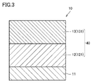
- FIG. 3 is a schematic cross-sectional view of a cutting tool in another aspect of this embodiment.
- FIG. 4 is a schematic cross-sectional view of a cutting tool in another aspect of this embodiment.
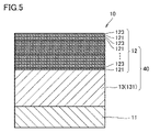
- FIG. 5 is a schematic cross-sectional view of a cutting tool in yet another aspect of this embodiment.
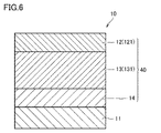
- FIG. 6 is a schematic cross-sectional view of a cutting tool according to the present embodiment including a base layer in the coating.
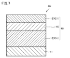
- FIG. 7 is a schematic cross-sectional view of a cutting tool according to this embodiment in which the coating includes an intermediate layer.
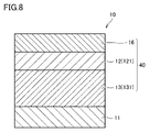
- FIG. 8 is a schematic cross-sectional view of a cutting tool according to this embodiment in which the coating includes a surface layer.
- FIG. 9 is an image diagram of a graph showing an example of the result of performing X-ray diffraction measurement on
- Cutting tools in recent years tend to be exposed to severe cutting conditions due to high-load cutting requirements.
- the current situation is that cutting tools that can be used stably under severe cutting conditions, in other words, cutting tools that have a sufficiently long life have not yet been provided.
- high-load cutting such as cutting of high-hardness materials such as hardened steel (especially high-load cutting such as intermittent cutting)
- the peeling resistance and chipping resistance may not be sufficient. Therefore, a cutting tool having a long tool life is demanded even in high-load cutting (especially high-load cutting such as interrupted cutting) like cutting of high-hardness materials such as hardened steel.
- an object of the present disclosure is to provide a cutting tool having a long tool life even in high-load cutting of high-hardness materials.
- a cutting tool comprising a substrate and a coating disposed on the substrate,
- the coating comprises a first layer and a second layer,
- the hardness H1 of the first layer is 25 GPa or more and 40 GPa or less,
- the hardness H 2 of the second layer satisfies 0.5 ⁇ H 1 ⁇ H 2 ⁇ 0.9 ⁇ H 1 .
- the cutting tool of the present disclosure can have a long tool life even in high-load cutting of high-hardness materials.
- the thickness of the first layer is preferably 0.2 ⁇ m or more and 10 ⁇ m or less. This further improves the wear resistance of the cutting tool.
- the thickness of the second layer is preferably 0.2 ⁇ m or more and 10 ⁇ m or less. This further improves the chipping resistance of the cutting tool and the peeling resistance of the cutting tool.
- the ratio T 1 /T 2 of the thickness T 1 of the first layer to the thickness T 2 of the second layer is preferably 0.02 or more and 50 or less. This further improves the balance of wear resistance, spallation resistance and chipping resistance of the cutting tool.
- X-ray diffraction intensity I of the (200) plane of the coating (200 ) X-ray diffraction intensity I of the (111) plane (111 )
- X-ray diffraction intensity I of the (220) plane (220) The ratio I (200) /(I (200) +I (111) +I (220) ) of I (200) to the sum of The ratio of I( 111) to the sum I (111) /(I (200) +I (111) +I (220) ), and the ratio of I( 220) to the sum I (220) /(I (200 ) ) +I (111) +I (220) ) is preferably 0.45 or more. This further improves the delamination resistance of the cutting tool.
- the first layer includes a first unit layer; the first unit layer is made of Ti x Al y M 1-xy C z N 1-z ;
- the M is one element selected from the group consisting of zirconium, hafnium, elements of Group 5 and Group 6 of the periodic table, silicon, boron, and yttrium,
- the x is 0.20 or more and 0.99 or less,
- the y is 0.01 or more and 0.80 or less,
- the 1-xy is 0.01 or more and 0.20 or less,
- the z is preferably 0 or more and 1 or less. This further improves the wear resistance of the cutting tool.
- the first layer further includes a second unit layer; the second unit layer is made of Al m Cr 1-m N, The m is 0 or more and 0.8 or less, The thickness of the first unit layer is 5 nm or more and 50 nm or less, The thickness of the second unit layer is 5 nm or more and 50 nm or less, Preferably, the first unit layers and the second unit layers are alternately laminated. This further improves the wear resistance of the cutting tool.
- the first layer further includes a third unit layer; the third unit layer is made of Ti 1-n Al n N, The n is 0 or more and 0.8 or less, The thickness of the first unit layer is 5 nm or more and 50 nm or less, The thickness of the third unit layer is 5 nm or more and 50 nm or less, Preferably, the first unit layers and the third unit layers are alternately laminated. This further improves the wear resistance of the cutting tool.
- the second layer includes a fourth unit layer; the fourth unit layer is made of TiaAlbCcN1 -c ,
- the a is 0.2 or more and 1.0 or less,
- the b is 0 or more and 0.8 or less,
- Said c is preferably 0 or more and 1 or less. This further improves the chipping resistance of the cutting tool and the peeling resistance of the cutting tool.
- a compound or the like when represented by a chemical formula, it shall include any conventionally known atomic ratio unless the atomic ratio is particularly limited, and should not necessarily be limited only to those within the stoichiometric range.
- TiAlSiN when “TiAlSiN" is described, the ratio of the number of atoms constituting TiAlSiN includes all conventionally known atomic ratios.
- the cutting tool 10 As shown in FIGS. 2 and 3, the cutting tool 10 according to this embodiment has A cutting tool 10 comprising a substrate 11 and a coating 40 disposed on the substrate 11,
- the coating 40 includes a first layer 12 and a second layer 13,
- the hardness H1 of the first layer 12 is 25 GPa or more and 40 GPa or less
- the hardness H 2 of the second layer 13 satisfies 0.5 ⁇ H 1 ⁇ H 2 ⁇ 0.9 ⁇ H 1 .
- the cutting tool of the present disclosure can have a long tool life even in high-load cutting such as cutting of high-hardness materials such as hardened steel (especially high-load cutting such as interrupted cutting). The reason is presumed as follows.
- the coating includes a first layer, and the hardness H1 of the first layer 12 is 25 GPa or more and 40 GPa or less. This allows such cutting tools to have excellent wear resistance.
- wear resistance means resistance to abrasion of the coating when used for cutting.
- the coating includes a first layer, and the hardness H1 of the first layer 12 is 25 GPa or more and 40 GPa or less.
- a coating having the above hardness is excellent in wear resistance.
- such a coating is generally highly brittle, it tends to be easily damaged (chipping of the coating and peeling of the coating) by breaking the coating itself. For this reason, in cutting tools having such a coating, the coating itself is destroyed during high-load cutting such as cutting of high-hardness materials such as hardened steel (especially high-load cutting such as interrupted machining). Damage tends to occur, and wear tends to progress starting from the damage.
- the coating has the second layer together with the first layer, and the hardness H2 of the second layer 13 is 0.5 ⁇ H 1 ⁇ H 2 ⁇ 0.9 ⁇
- H1 the hardness of the coating as a whole can be suppressed to a low level, so that damage caused by destruction of the coating itself (fine cracks and peeling of the coating) can be suppressed.
- the cutting tool of the present embodiment has excellent peeling resistance and excellent resistance even in high-load cutting such as cutting of high-hardness materials such as hardened steel (particularly, high-load cutting such as interrupted cutting). It has a chipping property and can suppress the progress of wear originating from film damage.
- peeling resistance means resistance to peeling of the coating from the substrate.
- chipping resistance used herein means resistance to occurrence of minute cracks in the film.
- the cutting tool according to this embodiment can have a long tool life by combining excellent wear resistance, excellent flaking resistance, and excellent chipping resistance.
- the shape and application of the cutting tool 10 according to this embodiment are not particularly limited.
- the cutting tool 10 according to the present embodiment includes a drill, an end mill, an indexable cutting insert for a drill, an indexable cutting insert for an end mill, an indexable cutting insert for milling, an indexable cutting insert for turning, It can be a metal saw, a gear cutting tool, a reamer, a tap, a tip for crankshaft pin milling, and the like.
- FIG. 1 is a perspective view illustrating one aspect of the cutting tool 10 of the present disclosure.
- the cutting tool 10 having such a shape is used as an indexable cutting tip such as an indexable cutting tip for turning.
- the base material may be a cemented carbide (for example, a tungsten carbide (WC)-based cemented carbide, a cemented carbide containing Co in addition to WC, or a carbonitride such as Ti, Ta, Nb, etc. added in addition to WC). cemented carbide, etc.), cermets (having TiC, TiN, TiCN, etc.
- a cemented carbide for example, a tungsten carbide (WC)-based cemented carbide, a cemented carbide containing Co in addition to WC, or a carbonitride such as Ti, Ta, Nb, etc. added in addition to WC.
- cemented carbide, etc. cemented carbide, etc.
- cermets having TiC, TiN, TiCN, etc.
- high-speed steels high-speed steels, tool steels, ceramics (TiC, SiC, SiN, AlN, Al2O3 , sialon, and their mixture, etc.), a cubic boron nitride sintered body (cBN sintered body), a diamond sintered body, and a hard material in which cubic boron nitride particles are dispersed in the binding phase. preferably included.
- cemented carbide especially WC-based cemented carbide
- cermet especially TiCN-based cermet
- the effect of the present embodiment is exhibited even if such a cemented carbide contains free carbon or an abnormal phase called ⁇ phase in the structure.
- the base material used in this embodiment may have a modified surface.
- a ⁇ -free layer may be formed on the surface, or in the case of a cBN sintered body, a surface-hardened layer may be formed. Even if the surface is modified in this way, The effect of this embodiment is shown.
- the substrate may or may not have a chip breaker. included.
- the shape of the cutting edge is sharp edge (the ridge where the rake face and flank face intersect), honing (sharp edge rounded), negative land (chamfered shape), and a combination of honing and negative land. includes any shape.
- FIG. 2 is a schematic cross-sectional view illustrating one aspect of the cutting tool of the present disclosure.
- FIG. 3 is a schematic cross-sectional view illustrating another aspect of the cutting tool of the present disclosure.
- the "coating" covers at least the cutting edge portion of the base material 11, thereby improving various properties of the cutting tool such as peeling resistance, chipping resistance, and wear resistance.
- the cutting edge portion described here means a region within 500 ⁇ m along the substrate surface from the cutting edge ridgeline.
- the coating 40 preferably covers the entire surface of the substrate 11 . However, even if a part of the substrate 11 is not covered with the film 40 or the structure of the film 40 is partially different, this does not depart from the scope of the present embodiment.
- the thickness of the coating is preferably 0.1 ⁇ m or more and 30 ⁇ m or less, more preferably 0.4 ⁇ m or more and 20 ⁇ m or less, further preferably 0.5 ⁇ m or more and 10 ⁇ m or less, and 0.7 ⁇ m or more and 5 ⁇ m or less. is even more preferable, and it is particularly preferable to be 1 ⁇ m or more and 3 ⁇ m or less.
- the thickness of the coating means the sum of the thicknesses of the layers constituting the coating. Examples of "layers constituting the coating" include the first layer, the second layer, and other layers described later as layers other than the first layer and the second layer.
- the thickness of the coating is, for example, using a scanning electron microscope (SEM), measuring arbitrary 5 points in a cross-sectional sample parallel to the normal direction of the surface of the base material, and measuring 5 points It is possible to obtain by taking the average value of the thickness.
- SEM scanning electron microscope
- a focused ion beam device, a cross-section polisher device, or the like can be used to prepare the cross-sectional sample. The same applies when measuring the thickness of each of the first layer, the second layer, the first unit layer, the second unit layer, the third unit layer, the fourth unit layer, and the other layers. be.
- the coating includes a first layer and a second layer.
- a plurality of the first layers may be provided as long as the effect of the cutting tool is maintained.
- the said 2nd layer may be provided in multiple numbers.
- either the first layer or the second layer may be positioned closest to the surface.
- either the first layer or the second layer may be positioned closest to the substrate.
- “including a first layer and a second layer” means that the coating can include other layers described later as layers other than the first layer and the second layer.
- variations in the orientation between the first layer and the second layer arranged closest to the first layer can be suppressed, and the orientation can be made uniform.
- the “X-ray diffraction intensity I (200) of the (200) plane” means the diffraction intensity (peak height) at the highest peak among the X-ray diffraction peaks derived from the (200) plane (hereinafter , also referred to as “maximum diffraction intensity”).
- each of the two or more compounds contained in the film has an X-ray diffraction peak A1 derived from the (200) plane and an X-ray diffraction peak A2 derived from the (200) plane.
- the “X-ray diffraction intensity I (200) of the (200) plane” is the maximum diffraction intensity (peak height). The same applies to the “(111) plane X-ray diffraction intensity I (111) " and “(220) plane X-ray diffraction intensity I (220) ".
- I (200) /(I (200) +I (111) +I (220) ), I (111) /(I (200) +I (111) +I (220) ), and I (220) /(I (200) +I (111) +I (220) ) is preferably 0.47 or more, more preferably 0.50 or more, and preferably 0.55 or more More preferred.
- I (200) /(I (200) +I (111) +I (220) ), I (111) /(I (200) +I (111) +I (220) ), and I (220) /(I (200) +I (111) +I (220) ) is preferably 0.90 or less, more preferably 0.85 or less, and preferably 0.80 or less. More preferred.
- I (200) /(I (200) +I (111) +I (220) ), I (111) /(I (200) +I (111) +I (220) ), and I (220) /(I (200) +I (111) +I (220) ) is preferably 0.47 or more and 0.90 or less, more preferably 0.50 or more and 0.85 or less, It is more preferably 0.55 or more and 0.80 or less.
- the above I (200) , I (111) , and I (220) can be determined, for example, by X-ray diffraction measurement (XRD measurement) under the following conditions. Specifically, the surface of the coating is irradiated with X-rays, X-ray diffraction measurement (XRD measurement) is performed, and the X-ray diffraction intensities of the (200) plane, (111) plane and (220) plane are obtained, The above I (200) , the above I (111) , and the above I (220) are calculated. Examples of the apparatus used for the X-ray diffraction measurement include "SmartLab" (trade name) manufactured by Rigaku Corporation and "X'pert" (trade name) manufactured by Panalytical.
- the hardness H1 of the first layer according to this embodiment is 25 GPa or more and 40 GPa or less. This allows the cutting tool to have excellent wear resistance.
- the lower limit of H1 is preferably 27 GPa or more, more preferably 29 GPa or more, and even more preferably 31 GPa or more.
- the upper limit of H1 is preferably 38 GPa or less, more preferably 36 GPa or less, and even more preferably 34 GPa or less. Further, H1 is preferably 27 GPa or more and 38 GPa or less , more preferably 29 GPa or more and 36 GPa or less, and even more preferably 31 GPa or more and 34 GPa or less.
- the hardness H1 of the first layer is measured by a method conforming to ISO14577 (2015) to measure the indentation hardness.
- a nanoindentation hardness tester (ENT1100a; manufactured by Elionix) is used as a measuring instrument. Specifically, first, the position of the cutting tool where the coating is provided is ground so as to obtain a surface (inclined surface) having an inclination of 6° with respect to the surface direction of the outermost surface of the coating. Next, at an arbitrary point on the surface of the first layer on the obtained inclined surface and corresponding to the middle point in the film thickness direction of the first layer, under an environment of 25 ° C.
- the hardness H1 of the first layer is calculated according to ISO14577. The same is true when measuring the hardness H2 of the second layer.
- the hardness H1 of the first layer means the hardness of the entire first layer.
- the thickness of the first layer is preferably 0.2 ⁇ m or more and 10 ⁇ m or less. This can further improve the wear resistance of the cutting tool.
- the lower limit of the thickness of the first layer is preferably 0.4 ⁇ m or more, more preferably 0.5 ⁇ m or more, and even more preferably 0.6 ⁇ m or more.
- the upper limit of the thickness of the first layer is preferably 6 ⁇ m or less, more preferably 3 ⁇ m or less, and even more preferably 2 ⁇ m or less.
- the thickness of the first layer is preferably 0.4 ⁇ m or more and 6 ⁇ m or less, more preferably 0.5 ⁇ m or more and 3 ⁇ m or less, and even more preferably 0.6 ⁇ m or more and 2 ⁇ m or less.
- the first layer includes a first unit layer, and the first unit layer is made of Ti x Al y M 1-xy C z N 1-z , and M is zirconium, hafnium, or an element selected from the group consisting of Group 5 elements, Group 6 elements, silicon, boron, and yttrium, x is 0.20 or more and 0.99 or less, and y is 0.01 0.80 or less, 1-xy is 0.01 or more and 0.20 or less, and z is preferably 0 or more and 1.0 or less. This can further improve the wear resistance of the cutting tool.
- the first layer includes the first unit layer
- the first layer means that the first layer consists of only the first unit layer, and that the first layer and the first unit layer together with the second unit layer or It is a concept that includes aspects including a third unit layer.
- the first unit layer consists of Ti x Al y M 1-x-y C z N 1-z
- the first unit layer consists of Ti x Al y M 1-x-y C z N 1-z
- x is preferably 0.25 or more and 0.95 or less, more preferably 0.30 or more and 0.90 or less, and still more preferably 0.35 or more and 0.80 or less.
- y is preferably 0.10 or more and 0.70 or less, more preferably 0.20 or more and 0.60 or less, and still more preferably 0.30 or more and 0.55 or less.
- the 1-xy is preferably 0.02 or more and 0.18 or less, more preferably 0.03 or more and 0.15 or less, and 0.04 or more and 0.10 or less. is more preferred.
- the above z is preferably 0.01 or more and 0.90 or less, more preferably 0.05 or more and 0.70 or less, and still more preferably 0.10 or more and 0.50 or less.
- x is 0.20 or more and 0.99 or less
- y is 0.01 or more and 0.80 or less
- 1-xy is 0, and Said z can also be 0 or more and 1.0 or less.
- 1-xy is preferably not "0".
- the above x, above y, and above z can be confirmed by using an EDX (Energy Dispersive X-ray spectroscopy) device attached to SEM or TEM. Specifically, first, a cutting tool is cut at an arbitrary position in the film thickness direction to prepare a sample including a cross section of the film. Next, point analysis is performed on the first unit layer in the coating. Note that the measurement point is on the middle point in the thickness direction of the first unit layer so that the information near the interface is not included. The measurements are performed at five arbitrarily selected locations. Specify x and y, which indicate the atomic ratio of each element, at each of the five arbitrary measurement points. An average value of each of x and y is obtained at five measurement points. The average value corresponds to x and y above in the first unit layer. The same is true for obtaining m in the second unit layer described later, n in the third unit layer described later, and a, b, and c in the fourth unit layer described later.
- the thickness of the first unit layer is preferably 0.2 ⁇ m or more and 10 ⁇ m or less. This can further improve the wear resistance of the cutting tool. Further, when the first layer consists of only the first unit layer, the lower limit of the thickness of the first unit layer is preferably 0.4 ⁇ m or more, more preferably 0.5 ⁇ m or more, and 0 0.6 ⁇ m or more is more preferable. When the first layer consists of only the first unit layer, the upper limit of the thickness of the first unit layer is preferably 6 ⁇ m or less, more preferably 3 ⁇ m or less, and 2 ⁇ m or less. is more preferred.
- the thickness of the first unit layer is preferably 0.4 ⁇ m or more and 6 ⁇ m or less, more preferably 0.5 ⁇ m or more and 3 ⁇ m or less. , more preferably 0.6 ⁇ m or more and 2 ⁇ m or less.
- the thickness of the first unit layer is preferably 0.005 ⁇ m or more and 1 ⁇ m or less. This can further improve the wear resistance of the cutting tool.
- the lower limit of the thickness of the first unit layer is preferably 0.007 ⁇ m or more. , more preferably 0.010 ⁇ m or more, and even more preferably 0.015 ⁇ m or more.
- the upper limit of the thickness of the first unit layer is preferably 0.8 ⁇ m or less.
- the thickness of the first unit layer is 0.005 ⁇ m or more and 0.8 ⁇ m or less. , more preferably 0.010 ⁇ m or more and 0.6 ⁇ m or less, and even more preferably 0.015 ⁇ m or more and 0.3 ⁇ m or less.
- the first layer 12 further includes a second unit layer 13 together with the first unit layer.
- the second unit layer 13 is made of Al m Cr 1-m N, m is 0 or more and 0.8 or less, and the thickness of the first unit layer 121 is 5 nm or more and 50 nm or less. and the thickness of the second unit layer 122 is 5 nm or more and 50 nm or less, and the first unit layer 121 and the second unit layer 122 are preferably alternately laminated (FIG. 4).
- the grain size of the particles constituting the first layer becomes finer, the hardness of the first layer increases, so that the wear resistance of the cutting tool can be further improved.
- the first unit layer and the second unit layer are alternately laminated
- either one of the first unit layer and the second unit layer may be arranged closest to the substrate.
- the first unit layer and the second unit layer may be arranged on the most surface side.
- the phrase “the second unit layer is made of Al m Cr 1-m N” is not limited to the embodiment made only of Al m Cr 1-m N, and as long as the effects of the present disclosure are exhibited, It is a concept that includes aspects including components other than Al m Cr 1-m N (for example, unavoidable impurities) in addition to Al m Cr 1-m N.
- m is preferably 0.10 or more and 0.75 or less, more preferably 0.20 or more and 0.73 or less, and still more preferably 0.30 or more and 0.70 or less.
- the thickness of the second unit layer is preferably 5 nm or more and 1 ⁇ m or less. This can further improve the wear resistance of the cutting tool.
- the lower limit of the thickness of the second unit layer is preferably 7 nm or more, more preferably 10 nm or more, and even more preferably 15 nm or more.
- the upper limit of the thickness of the second unit layer is preferably 0.8 ⁇ m or less, more preferably 0.6 ⁇ m or less, and even more preferably 0.3 ⁇ m or less.
- the thickness of the second unit layer is preferably 5 nm or more and 0.8 ⁇ m or less, more preferably 10 nm or more and 0.6 ⁇ m or less, and even more preferably 15 nm or more and 0.3 ⁇ m or less.
- the first layer 12 further includes a third unit layer 123 together with the first unit layer.
- the third unit layer 123 is made of Ti 1-n Al n N, n is 0 or more and 0.8 or less, and the thickness of the first unit layer 121 is 5 nm or more and 50 nm or less. and the thickness of the third unit layer 123 is 5 nm or more and 50 nm or less, and the first unit layer 121 and the third unit layer 123 are preferably alternately laminated (FIG. 5).
- the third unit layer 123 is made of Ti 1-n Al n N, n is 0 or more and 0.8 or less, and the thickness of the first unit layer 121 is 5 nm or more and 50 nm or less. and the thickness of the third unit layer 123 is 5 nm or more and 50 nm or less, and the first unit layer 121 and the third unit layer 123 are preferably alternately laminated (FIG. 5).
- the phrase “the third unit layer is made of Ti 1-n Al n N” is not limited to the mode of being made only of Ti 1-n Al n N, and as long as the effects of the present disclosure are achieved, It is a concept that includes an aspect including Ti 1 -n Al n N and components other than Ti 1-n Al n N (for example, unavoidable impurities).
- n is preferably 0.3 or more and 0.9 or less, more preferably 0.4 or more and 0.8 or less, and still more preferably 0.5 or more and 0.7 or less.
- the thickness of the third unit layer is preferably 5 nm or more and 1 ⁇ m or less. This can further improve the wear resistance of the cutting tool.
- the lower limit of the thickness of the third unit layer is preferably 7 nm or more, more preferably 10 nm or more, and even more preferably 15 nm or more.
- the upper limit of the thickness of the third unit layer is preferably 0.8 ⁇ m or less, more preferably 0.6 ⁇ m or less, and even more preferably 0.3 ⁇ m or less.
- the thickness of the third unit layer is preferably 5 nm or more and 0.8 ⁇ m or less, more preferably 10 nm or more and 0.6 ⁇ m or less, and even more preferably 15 nm or more and 0.3 ⁇ m or less.
- the hardness H 2 of the second layer according to this embodiment satisfies 0.5 ⁇ H 1 ⁇ H 2 ⁇ 0.9 ⁇ H 1 . This allows the cutting tool to have excellent flaking resistance and excellent chipping resistance.
- the above H 2 preferably satisfies H 2 ⁇ 0.53 ⁇ H 1 , more preferably satisfies H 2 ⁇ 0.56 ⁇ H 1 , and further satisfies H 2 ⁇ 0.6 ⁇ H 1 preferable.
- H 2 preferably satisfies H 2 ⁇ 0.87 x H 1 , more preferably satisfies H 2 ⁇ 0.84 x H 1 , and satisfies H 2 ⁇ 0.8 x H 1 is more preferred.
- the above H 2 preferably satisfies 0.53 ⁇ H 1 ⁇ H 2 ⁇ 0.87 ⁇ H 1 , more preferably 0.56 ⁇ H 1 ⁇ H 2 ⁇ 0.84 ⁇ H 1 .
- 0.6 ⁇ H 1 ⁇ H 2 ⁇ 0.8 ⁇ H 1 is more preferably satisfied.
- the thickness of the second layer is preferably 0.2 ⁇ m or more and 10 ⁇ m or less. Thereby, the chipping resistance of the cutting tool and the peeling resistance of the cutting tool can be further improved.
- the lower limit of the thickness of the second layer is preferably 0.3 ⁇ m or more, more preferably 0.4 ⁇ m or more, and even more preferably 0.5 ⁇ m or more.
- the upper limit of the thickness of the second layer is preferably 8 ⁇ m or less, more preferably 5 ⁇ m or less, and even more preferably 3 ⁇ m or less.
- the thickness of the second layer is preferably 0.3 ⁇ m or more and 8 ⁇ m or less, more preferably 0.4 ⁇ m or more and 5 ⁇ m or less, and even more preferably 0.5 ⁇ m or more and 3 ⁇ m or less.
- the ratio T 1 /T 2 of the thickness T 1 of the first layer to the thickness T 2 of the second layer is preferably 0.02 or more and 50 or less.
- the lower limit of T 1 /T 2 is preferably 0.04 or more, more preferably 0.06 or more, and even more preferably 0.1 or more.
- the upper limit of T 1 /T 2 is preferably 45 or less, more preferably 40 or less, and even more preferably 30 or less.
- the second layer preferably includes the fourth unit layer.
- the fourth unit layer is made of Ti a Al b C c N 1-c , the a is 0.2 or more and 1.0 or less, and the b is 0 or more and 0.8 or less. and c is preferably 0 or more and 1.0 or less.
- the second layer includes the fourth unit layer
- the second layer consists only of the fourth unit layer, and that the second layer is a layer other than the fourth unit layer together with the fourth unit layer.
- the fourth unit layer is composed of Ti a Al b C c N 1-c
- the fourth unit layer is not limited to the mode composed only of Ti a Al b C c N 1-c , and the effect of the present disclosure is exhibited.
- the thickness of the fourth unit layer is preferably 0.3 ⁇ m or more and 9 ⁇ m or less. This can further improve the wear resistance of the cutting tool.
- the lower limit of the thickness of the fourth unit layer is preferably 0.4 ⁇ m or more, more preferably 0.5 ⁇ m or more, and even more preferably 0.6 ⁇ m or more.
- the upper limit of the thickness of the fourth unit layer is preferably 7 ⁇ m or less, more preferably 5 ⁇ m or less, and even more preferably 3 ⁇ m or less.
- the thickness of the fourth unit layer is preferably 0.4 ⁇ m or more and 7 ⁇ m or less, more preferably 0.5 ⁇ m or more and 5 ⁇ m or less, and even more preferably 0.6 ⁇ m or more and 3 ⁇ m or less.
- the above a is preferably 0.3 or more and 0.95 or less, more preferably 0.35 or more and 0.9 or less, and even more preferably 0.4 or more and 0.85 or less.
- the above b is preferably 0.05 or more and 0.7 or less, more preferably 0.1 or more and 0.65 or less, and still more preferably 0.15 or more and 0.6 or less.
- the above c is preferably 0.01 or more and 0.9 or less, more preferably 0.03 or more and 0.85 or less, and still more preferably 0.05 or more and 0.7 or less.
- the coating may further include the other layers as long as the effects of the present embodiment are not impaired.
- examples of the other layers include an underlying layer 14, an intermediate layer 15, a surface layer 16, and the like.
- the coating of this embodiment can include an underlayer.
- the base layer 14 is a layer arranged between the substrate 11 and the layer closest to the substrate among the first layer 12 and the second layer 13 .
- the underlayer is composed of a first compound, and the first compound includes one or more elements selected from the group consisting of elements of Group 4, Group 5, Group 6 of the periodic table, and aluminum, and carbon, nitrogen, and boron. and one or more elements selected from the group consisting of oxygen. This can further improve the wear resistance of the cutting tool. In addition, this can also improve the adhesion between the coating and the substrate.
- the adhesion between the substrate and the coating can be enhanced.
- the thickness of the underlayer is preferably 0.1 ⁇ m or more and 20 ⁇ m or less. This can further improve the wear resistance of the cutting tool. This also allows the cutting tool to have excellent chipping resistance.
- the coating of this embodiment can include an intermediate layer.
- the intermediate layer 15 is a layer arranged between the first layer 12 and the second layer 13 .
- the composition of the intermediate layer is preferably a TiAlN layer or a TiN layer, for example.
- the thickness of the intermediate layer is preferably 0.01 ⁇ m or more and 0.2 ⁇ m or less.
- the coating of this embodiment can include a surface layer.
- the surface layer 16 is the layer located closest to the surface of the coating 40 . However, it may not be formed at the cutting edge ridge.
- the surface layer 16 is composed of a second compound, and the second compound includes at least one element selected from the group consisting of Group 4 elements, Group 5 elements, Group 6 elements of the periodic table, and aluminum, carbon, nitrogen, and one or more elements selected from the group consisting of boron and oxygen. This can further improve the wear resistance of the cutting tool.
- the surface layer 16 may be a TiN layer or a TiAlN layer. Since the TiN layer has a clear color (golden color), its use as the surface layer 16 has the advantage of facilitating identification of the corners of the cutting tip after use for cutting (identification of used portions). By using a TiAlN layer as the surface layer 16, the oxidation resistance of the coating can be enhanced.
- the thickness of the surface layer 16 is preferably 0.05 ⁇ m or more and 1 ⁇ m or less. This improves the adhesion between the surface layer 16 and adjacent layers.
- Embodiment 2 Manufacturing method of cutting tool
- a method for manufacturing the cutting tool of Embodiment 1 will be described below.
- the following manufacturing method is an example, and the cutting tool of Embodiment 1 may be manufactured by other methods.
- the method for manufacturing a cutting tool includes: A first step of preparing the base material (hereinafter sometimes simply referred to as “first step”); and a second step of forming the coating on the base material (hereinafter sometimes simply referred to as “second step”). Each step will be described below.
- the substrate is prepared.
- any base material can be used as long as it is conventionally known as this type of base material, as described above.
- a tool made of a cubic boron nitride sintered body whose shape is ISO standard DNGA150408 can be used.
- ⁇ Second step Step of forming a coating on the base material>>
- a coating is formed on the substrate.
- the second step includes a "first layer coating step” of coating at least a portion of the surface of the base material with a first layer, and a “coating step of coating at least a portion of the surface of the base material with a second layer.” second layer coating step”.
- first layer coating step and the second layer coating step are performed, either one of the first layer coating step and the second layer coating step may be performed first.
- the second step can further include at least one of step (i), step (ii), and step (iii), which will be described later.
- the second step may further include an "other layer coating step” of coating at least part of the surface of the base material with the other layer.
- the terms “coated with the first layer” or “coated with the second layer” herein refer to the case where the first layer or the second layer covers directly above the substrate surface, and the case where the substrate surface and the first layer Or, it is a concept that includes both the case where a layer (base layer) other than the first layer or the second layer is arranged between the layer and the second layer. Either the first layer coating step or the second layer coating step may be performed first.
- the first layer coating step can include a "first unit layer coating step” of forming a first unit layer in the first layer.
- the first layer coating step further includes a "second unit layer coating step” for forming a second unit layer in the first layer, or a "third unit layer coating step” for forming a third unit layer in the first layer. process” can be included.
- the second layer coating step can include a "fourth unit layer coating step” of forming a fourth unit layer in the second layer.
- the second step can include an "other layer coating step” for forming the other layer.
- Examples of methods for coating at least part of the base material with the first layer include physical vapor deposition (PVD). The same applies to the first unit layer covering step, the second unit layer covering step, the third unit layer covering step, the second unit layer covering step, and the fourth unit layer covering step.
- PVD physical vapor deposition
- Examples of physical vapor deposition methods include sputtering, ion plating, arc ion plating, and electron ion beam evaporation.
- sputtering ion plating
- arc ion plating arc ion plating
- electron ion beam evaporation electron ion beam evaporation.
- the cathodic arc ion plating method or sputtering method which has a high ion rate of the raw material element, it is possible to subject the substrate surface to metal or gas ion bombardment treatment before forming the coating. It is preferable because the adhesion to is markedly improved.
- the following conditions can be mentioned.
- a Ti target is used as the metal evaporation source, and N 2 gas is used as the reaction gas.
- the substrate (base material) temperature is set at 400-550° C. and the gas pressure in the apparatus is set at 0.3-1.5 Pa.
- An apparatus used for the arc ion plating method includes, for example, AIP (trade name) manufactured by Kobe Steel, Ltd.
- a Ti target can be used as a metal evaporation source, and a sputtering gas such as N 2 gas, Ar gas, Kr gas, or Xe gas can be used as a reaction gas.
- the present inventors newly found that the hardness difference between the first layer and the second layer can be adjusted by performing at least one of the following steps (i) to (iii). I found out.
- at least one of the above steps (i) to (iii) is performed even when the difference in hardness between the first layer and the second layer is outside the desired range under conventional film formation conditions due to the chemical composition. It has been found that the difference in hardness between the first layer and the second layer can be easily adjusted by this.
- step (i) the second layer is annealed with a heater for a certain period of time.
- the hardness of the second layer can be lowered, so that the hardness H2 of the second layer can be adjusted within the range of 0.5 ⁇ H 1 ⁇ H 2 ⁇ 0.9 ⁇ H 1 . .
- the rate of temperature increase in step (i) is, for example, 5° C./min or more and 10° C./min or less.
- the annealing temperature in the step (i) is, for example, 400° C. or higher and 500° C. or lower.
- the annealing time in the step (i) is, for example, 10 minutes or more and 60 minutes or less.
- the cooling rate in the step (i) is, for example, 5° C./min or more and 10° C./min or less.
- the pressure in the furnace during cooling in the step (i) is, for example, 1 Pa or more and 8 Pa or less.
- the first layer or the second layer is subjected to ion bombardment treatment using a sputtering gas.
- a sputtering gas As a result, compressive stress can be applied to the first layer or the second layer, so that the hardness of the first layer or the second layer subjected to the ion bombardment treatment can be increased.
- the gas composition in the above step (ii) is, for example, Ar (100%), Kr (100%), or Xe (100%).
- the gas pressure in the step (ii) is, for example, 1 Pa or more and 3 Pa or less.
- the bias voltage in the step (ii) is, for example, -1000 V or more and -600 V or less.
- the treatment time in the step (ii) is, for example, 5 minutes or more and 60 minutes or less.
- step (iii) the first unit layers and the second or third unit layers are alternately laminated.
- lattice constant distortion occurs between layers having different compositions, so that the hardness of the first layer can be adjusted.
- the bias voltage is adjusted as follows when switching between the second layer coating step and the first layer coating step.
- A(V) be the bias voltage for the second layer coating process
- B(V) be the bias voltage for the first coating process.
- the bias voltage is set to A (V)
- the second layer coating step is performed.
- the bias voltage is greater than A and less than B (V) when B>A, or when A>B.
- Time is changed to more than B and less than A (V), and film formation is performed for 60 to 120 seconds. This step is shown as step (iv-1).
- step (iv) includes one or both of step (iv-1) and step (iv-2).
- step (iv-3) A case in which the first layer coating process is performed first and then the second layer coating process is performed.
- B(V) be the bias voltage for the first layer coating process
- A(V) the bias voltage for the second coating process.
- the bias voltage is set to B (V)
- the first layer coating step is performed.
- the bias voltage is greater than A and less than B (V) when B>A, or when A>B.
- Time is changed to more than B and less than A (V), and film formation is performed for 60 to 120 seconds. This step is shown as step (iv-3).
- step (iv) includes one or both of step (iv-3) and step (iv-4).
- bias voltage B (V) in the first layer coating step is not more than 20 V and less than 60 V, it tends to be difficult to obtain the desired hardness H1.
- step (iv) changes in the bias voltage when switching from the first layer coating step to the second layer coating step and when switching from the second layer coating step to the first layer coating step can be moderated, it is possible to suppress variations in orientation in the film caused by abrupt changes in the bias voltage during film formation.
- the present inventors have newly discovered that the variation in orientation in the film can be suppressed by switching the bias voltage as described above.
- a “lower layer” is formed between the base material and the first layer.
- stratum covering step "intermediate layer covering step” for forming an intermediate layer between the first layer and the second layer, and “surface layer covering step” for forming a surface layer on the second layer, etc. may be performed as appropriate.
- the other layers may be formed by conventional methods. Specifically, for example, the other layer may be formed by the PVD method described above.
- a surface treatment step may be performed as appropriate.
- the surface treatment step include surface treatment using a medium in which diamond powder is supported on an elastic material.
- Example 1 ⁇ Manufacturing cutting tools ⁇ [Sample No. 1-1 to Sample No. 1-16, sample no. 1-18 to sample No. 1-35, and sample no. 1-101 to sample No. 1-105] Sample no. 1-1 to Sample No. 1-16, sample no. 1-18 to sample No. 1-35, and sample no. 1-101 to sample No. 1-105 was produced.
- ⁇ Step of preparing base material First, as a substrate preparation step, a cubic boron sintered body tool (shape: JIS standard DNGA150408) was prepared as a substrate. Next, the substrate was set at a predetermined position of an arc ion plating apparatus (manufactured by Kobe Steel, Ltd., trade name: AIP).
- a second layer coating step a second layer was formed on the surface of the substrate using an arc ion plating method under the conditions shown in Table 1. Specifically, the following method was used.
- the metal evaporation source a target corresponding to the "composition" of the second layer described in Tables 3 and 4, which will be described later, was used.
- the composition of the second layer was TiAlN
- a TiAl target was used as the metal evaporation source.
- TiCN, TiC or TiN a Ti target was used as the metal evaporation source.
- N2 gas and/or methane gas was used as the reaction gas.
- the substrate (substrate) temperature was set at 500° C. and the gas pressure in the apparatus was set at 1 Pa.
- step (i) the surface of the second layer was annealed under the conditions described in the "annealing temperature [°C]/time [minutes]” column of Table 1.
- the furnace pressure during annealing was set to 2 Pa.
- "-" in the "annealing temperature [°C]/time [minutes]” column of Table 1 means that step (i) was not performed.
- step (ii) ion bombardment treatment was performed under the conditions described in the "ion bombardment” column of Table 1.
- Ar (800V) means that the reaction gas is Ar gas and the bias voltage is 800V.
- the ion bombardment treatment time was 45 minutes, and the furnace pressure was 1 Pa.
- a "-" in the “ion bombardment” column of Table 1 means that step (ii) was not performed.
- step (iv) while maintaining the conditions other than the bias voltage, the bias voltage is changed from the bias voltage value in the second layer coating step to the bias voltage described in the "step (iv)" column of Table 1.
- the film was formed for 60 seconds by adjusting the bias voltage to the value.
- the bias voltage was adjusted from 30 V (bias voltage in the second layer coating step) to 33 V (bias voltage in step (iv)).
- the film formation conditions other than the bias voltage were changed to the first layer coating conditions shown below, and film formation was carried out for 60 seconds while maintaining the bias voltage.
- the arc ion plating method was used under the conditions shown in Table 1 to form the first layer on the second layer. Specifically, the following method was used.
- the metal evaporation source a target corresponding to the "composition" of the first layer described in Tables 3 and 4, which will be described later, was used.
- the composition of the first layer was TiAlN
- a TiAl target was used as the metal evaporation source.
- a TiAlSi target was used as the metal evaporation source.
- N2 gas was used as the reaction gas.
- the substrate (substrate) temperature was set at 500° C. and the gas pressure in the apparatus was set at 4 Pa.
- Sample no. 1-17 cutting tools were produced.
- ⁇ Step of preparing base material> As a base material preparation step, the above sample No. A substrate identical to that of 1-1 was prepared and set at a predetermined position in an arc ion plating apparatus.
- an arc ion plating method was used to form a first layer on the substrate. Specifically, the following method was used.
- the metal evaporation source a target corresponding to the "composition" of the first layer described in Table 3, which will be described later, was used. That is, a TiAl target was used as a metal evaporation source. N2 gas was used as the reaction gas.
- the substrate (base material) temperature was set at 500° C. and the gas pressure in the apparatus was set at 2 Pa.
- step (iv) while maintaining the conditions other than the bias voltage, the bias voltage is changed from the bias voltage value in the first layer coating step to the bias voltage described in the "step (iv)" column of Table 2.
- the bias voltage was adjusted to the value
- the film formation conditions other than the bias voltage were changed to the second layer coating conditions shown below, and film formation was carried out for 60 seconds while maintaining the bias voltage.
- an arc ion plating method was used to form a second layer on the first layer.
- the metal evaporation source a target corresponding to the "composition" of the second layer described in Tables 3 and 4, which will be described later, was used. That is, a TiAl target was used as a metal evaporation source. N2 gas was used as the reaction gas.
- the substrate (base material) temperature was set at 500° C. and the gas pressure in the apparatus was set at 2 Pa.
- the work material was cut under the following cutting conditions. Next, when the cutting distance reached 50 m, the cutting tool and the work material which were in contact with each other were once separated. Then, three minutes after the separation, the work material was cut again under the following cutting conditions. These were repeated until the cutting distance reached 3 km. Next, the maximum wear amount of the flank face of the cutting tool when the cutting distance reached 3 km was measured as the maximum wear amount. A smaller maximum wear amount means that the cutting tool has a longer tool life even in high-load cutting. Further, the fact that the maximum wear amount is 290 ⁇ m or less means that the cutting tool has a long tool life even in high-load cutting.
- Sample no. 1-1 to Sample No. 1-35 correspond to examples.
- Sample no. 1-101 to sample No. 1-105 corresponds to a comparative example. From the results of Tables 3 and 4, sample No. corresponding to the example. 1-1 to Sample No.
- the cutting tool of 1-35 is a sample No. corresponding to the comparative example. 1-101 to sample No. It was confirmed that 1-105 has a longer tool life than 1-105 even in high-load cutting, such as cutting of high-hardness materials such as hardened steel. The reason for this is that sample no. 1-1 to Sample No.
- the first layer of the coating has high hardness and good wear resistance, and the coating includes the first layer and the second layer, so the coating has chipping resistance and peeling resistance. It is presumed that this is because the coating is less likely to break during cutting, and the wear originating there is suppressed.
- Example 2 ⁇ Manufacturing cutting tools ⁇ [Sample No. 2-1 to Sample No. 2-43] Sample no. 2-1 to Sample No. 2-43 cutting tools were made.
- the second layer coating step was carried out under the conditions shown in Tables 5 and 6, and the following targets were used as metal evaporation sources. 1-1 to Sample No. 1-16, sample no. 1-18 to sample No. 1-35, and sample no. 1-101 to sample No. A second layer was formed on the substrate using the arc ion plating method under the same conditions as in 1-105.
- the metal evaporation source a target corresponding to the "composition" of the second layer described in Table 7, which will be described later, was used. Specifically, when the composition of the second layer was TiAlN, a TiAl target was used as the metal evaporation source. In the case of TiCN or TiN, a Ti target was used as the metal evaporation source.
- step (iv) the bias voltage is adjusted from the value of the bias voltage in the second layer coating step to the bias voltage value described in the “step (iv)” column of Tables 5 and 6. Film formation was performed for seconds. Subsequently, the film formation conditions other than the bias voltage were changed to the first layer coating conditions shown below, and film formation was carried out for 60 seconds while maintaining the bias voltage. In addition, process (i) and process (ii) were not performed.
- the arc ion plating method is used under the conditions shown in Tables 5 and 6 to alternately perform the first unit layer coating step and the second unit layer coating step.
- a first layer was formed on the surface of the second layer.
- the metal evaporation source a target corresponding to the "composition" of the first layer described in Tables 7 and 8, which will be described later, was used. That is, when the composition of the first unit layer was TiAlN, a TiAl target was used as the metal evaporation source. Further, for example, when the composition of the first unit layer was TiAlSiN, a TiAlSi target was used as the metal evaporation source.
- composition of the second unit layer was AlCrN
- an AlCr target was used as the metal evaporation source.
- a Cr target was used as the metal evaporation source.
- N2 gas was used as the reaction gas.
- the substrate (substrate) temperature was set at 500° C. and the gas pressure in the apparatus was set at 4 Pa.
- the first unit layer covering process and the second unit layer covering process was executed first, and the second unit layer covering process was executed last. .
- the results obtained are shown in Tables 7 and 8, respectively.
- the relationship among the "first unit layer thickness", the "second unit layer thickness” and the “first layer thickness” is as follows.
- the first layer is formed by alternately laminating the first unit layer with a thickness of 15 nm and the second unit layer with a thickness of 10 nm, and the thickness T1 of the first layer is 2.5 ⁇ m. be.
- sample no. 2-1 to Sample No. 2-43 cutting tools correspond to examples.
- Sample no. 2-1 to Sample No. 2-43 corresponds to the example. From the results of Tables 7 and 8, sample No. corresponding to the example. 2-1 to Sample No. It was confirmed that the cutting tool of No. 2-43 has a long tool life even in high-load cutting such as cutting of high-hardness materials such as hardened steel. The reason for this, as in Example 1, is that sample No. 2-1 to Sample No. In the cutting tool of 2-43, the first layer of the coating has high hardness and good wear resistance, and the coating includes the first layer and the second layer, so the coating has chipping resistance and peeling resistance. It is presumed that this is because the coating is less likely to break during cutting, and the wear originating there is suppressed.
- Example 3 ⁇ Manufacturing cutting tools ⁇ [Sample No. 3-1 to Sample No. 3-43, and sample no. 3-101] Sample no. 3-1 to Sample No. 3-43, and sample no. 3-101 cutting tools were produced.
- ⁇ Step of preparing base material> As a base material preparation step, the above sample No. 1-1 to Sample No. 1-16, sample no. 1-18 to sample No. 1-35, and sample no. 1-101 to sample No. A substrate identical to that of No. 1-105 was prepared and set at a predetermined position in an arc ion plating apparatus.
- the second layer coating process was performed under the conditions shown in Tables 9 and 10, and the following targets were used as metal evaporation sources. 1-1 to Sample No. 1-16, sample no. 1-18 to sample No. 1-35, and sample no. 1-101 to sample No.
- a second layer was formed on the surface of the base material using the arc ion plating method under the same conditions as in 1-105.
- the metal evaporation source a target corresponding to the "composition" of the second layer described in Tables 11 and 12, which will be described later, was used. Specifically, when the composition of the second layer was TiAlN or TiAlC, a TiAl target was used as the metal evaporation source. When the composition of the second layer was TiCN, TiC or TiN, a Ti target was used as the metal evaporation source.
- step (i) the surface of the second layer was annealed under the temperature conditions described in the "annealing temperature [°C]” column of Tables 9 and 10. "-" in the “annealing temperature [°C]” column of Tables 9 and 10 means that step (i) was not performed.
- step (iv) the bias voltage in the second layer coating step was adjusted to the bias voltage described in the "step (iv)" column of Tables 9 and 10, and film formation was performed for 60 seconds. Subsequently, the film formation conditions other than the bias voltage were changed to the first layer coating conditions shown below, and film formation was carried out for 60 seconds while maintaining the bias voltage. Note that step (ii) was not performed.
- the first layer coating step the first unit layer coating step and the third unit layer coating step are alternately performed using the arc ion plating method under the conditions shown in Tables 9 and 10.
- a first layer was formed on the surface of the second layer. Specifically, the following method was used.
- the metal evaporation source a target corresponding to the "composition" of the first layer described in Tables 11 and 12, which will be described later, was used. That is, when the composition of the first unit layer was TiAlN, a TiAl target was used as the metal evaporation source. Further, for example, when the composition of the first unit layer was TiAlSiN, a TiAlSi target was used as the metal evaporation source.
- the composition of the third unit layer was TiAlN
- a TiAl target was used as the metal evaporation source.
- N2 gas was used as the reaction gas.
- the substrate (substrate) temperature was set at 500° C. and the gas pressure in the apparatus was set at 4 Pa.
- the first unit layer covering process and the third unit layer covering process was executed first, and the third unit layer covering process was executed last. .
- the results obtained are shown in Tables 11 and 12, respectively.
- the relationship among the "first unit layer thickness", "third unit layer thickness” and “first layer thickness” is as follows.
- sample 3-1 a first unit layer having a thickness of 10 nm and a third unit layer having a thickness of 15 nm are alternately laminated to form a first layer, and the thickness T1 of the first layer is 2.5 ⁇ m. be.
- the cutting tool of 3-43 corresponds to the example, sample no.
- the 3-101 cutting tool corresponds to a comparative example.
- Sample no. 3-1 to Sample No. 3-43 corresponds to the example. Moreover, sample no. 3-101 corresponds to a comparative example. From the results of Tables 11 and 12, sample No. corresponding to the example. 3-1 to Sample No. The cutting tool of 3-43 is sample No. 3 which corresponds to the comparative example. It was confirmed that 3-101 has a longer tool life than 3-101, even in high-load cutting such as cutting of high hardness materials such as hardened steel. The reason for this, as in Example 1, is that sample No. 3-1 to Sample No. In the cutting tool of 3-43, the first layer of the coating has high hardness and good wear resistance, and the coating includes the first layer and the second layer, so the coating has chipping resistance and peeling resistance. It is presumed that this is because the coating is less likely to break during cutting, and the wear originating there is suppressed.
- Example 4 ⁇ Manufacturing cutting tools ⁇ [Sample No. 4-1 to Sample No. 4-28] Sample no. 4-1 to Sample No. 4-28 cutting tools were made.
- composition of the second layer was TiAlN or TiAlC
- a Ti target and an Al target were used as metal evaporation sources.
- the composition of the second layer was TiCN or TiN
- a Ti target was used as the metal evaporation source.
- step (iv) the bias voltage is adjusted from the bias voltage value in the second layer coating step to the bias voltage value described in the "step (iv)" column of Table 13, and the film is formed for 60 seconds. did Subsequently, the film formation conditions other than the bias voltage were changed to the first layer coating conditions shown below, and film formation was carried out for 60 seconds while maintaining the bias voltage. In addition, process (i) and process (ii) were not performed.
- the first layer coating step the first unit layer coating step and the second unit layer coating step are alternately performed using the arc ion plating method under the conditions shown in Table 13.
- a first layer was formed on the surface of the second layer.
- the metal evaporation source a target corresponding to the "composition" of the first layer described in Table 14, which will be described later, was used. That is, when the composition of the first unit layer was TiAlN, a TiAl target was used as the metal evaporation source. Further, for example, when the composition of the first unit layer was TiAlSiN, a TiAlSi target was used as the metal evaporation source.
- composition of the second unit layer was AlCrN
- an AlCr target was used as the metal evaporation source.
- a Cr target was used as the metal evaporation source.
- N2 gas was used as the reaction gas.
- the substrate (substrate) temperature was set at 500° C. and the gas pressure in the apparatus was set at 4 Pa.
- the first unit layer covering process and the second unit layer covering process was executed first, and the second unit layer covering process was executed last. .
- step (iii) a series of steps composed of the second layer coating step to the first layer coating step are performed according to the number of repetitions of the second layer coating step to the first layer coating step in Table 13. was performed the number of times described in the section. For example, sample no. In 4-1, a series of steps from the second layer coating step to the first layer coating step were repeated three times. That is, sample no.
- the coating of 4-1 is formed by alternately stacking the second layers and the first layers, and includes three layers each of the second layers and the first layers.
- the “first unit layer thickness” indicates the thickness of one first unit layer
- the “second unit layer thickness” indicates the thickness of one second unit layer
- the “thickness of the first layer” is The thickness of the first layer of one layer is indicated
- the “thickness of the second layer” indicates the thickness of the second layer of one layer.
- the first layer is formed by alternately laminating the first unit layer with a thickness of 15 nm and the second unit layer with a thickness of 10 nm
- the thickness T1 of the first layer is 0.5 ⁇ m.
- the 4-28 cutting tool corresponds to the example.
- Sample no. 4-1 to Sample No. 4-28 corresponds to the example. From the results in Table 14, sample No. corresponding to the example. 4-1 to Sample No. It was confirmed that the 4-28 cutting tool has a long tool life even in high-load cutting such as cutting of high-hardness materials such as hardened steel. The reason for this, as in Example 1, is that sample No. 4-1 to Sample No. In the cutting tool of 4-28, the first layer of the coating has high hardness and good wear resistance, and the coating includes the first layer and the second layer, so the coating has chipping resistance and peeling resistance. It is presumed that this is because the coating is less likely to break during cutting, and the wear originating there is suppressed.
- Example 5 ⁇ Manufacturing cutting tools ⁇ [Sample No. 5-1 to Sample No. 5-28] Sample no. 5-1 to Sample No. 5-28 cutting tools were made.
- ⁇ Step of preparing base material> As a base material preparation step, the above sample No. 1-1 to Sample No. 1-16, sample no. 1-18 to sample No. 1-35, and sample no. 1-101 to sample No. A substrate identical to that of No. 1-105 was prepared and set at a predetermined position in an arc ion plating apparatus.
- composition of the second layer was TiAlN or TiAlC
- a TiAl target was used as the metal evaporation source.
- composition of the second layer was TiN
- a Ti target was used as the metal evaporation source.
- step (iv) the bias voltage is adjusted from the bias voltage value in the second layer coating step to the bias voltage value described in the "step (iv)" column of Table 15, and the film is formed for 60 seconds. did Subsequently, the film formation conditions other than the bias voltage were changed to the first layer coating conditions shown below, and film formation was carried out for 60 seconds while maintaining the bias voltage. In addition, process (i) and process (ii) were not performed.
- the first layer coating step the first unit layer coating step and the third unit layer coating step are alternately performed using the arc ion plating method under the conditions shown in Table 15.
- a first layer was formed on the surface of the second layer. Specifically, the following method was used.
- the metal evaporation source a target corresponding to the "composition" of the first layer described in Table 16, which will be described later, was used. That is, when the composition of the first unit layer was TiAlN, a TiAl target was used as the metal evaporation source. Further, for example, when the composition of the first unit layer was TiAlSiN, a TiAlSi target was used as the metal evaporation source.
- the composition of the third unit layer was TiAlN
- a TiAl target was used as the metal evaporation source.
- an Al target was used as the metal evaporation source.
- N2 gas was used as the reaction gas.
- the substrate (substrate) temperature was set at 500° C. and the gas pressure in the apparatus was set at 4 Pa.
- the first unit layer covering step and the second unit layer covering step the first unit layer covering step was performed first, and the third unit layer covering step was lastly performed. .
- step (iii) a series of steps composed of the second layer coating step to the first layer coating step are performed according to the number of repetitions of the second layer coating step to the first layer coating step in Table 15. was performed the number of times described in the section. For example, sample no. In 5-1, a series of steps from the second layer coating step to the first layer coating step were repeated three times. That is, sample no. In the coating of 5-1, the second layers and the first layers are alternately laminated, and the second layers and the first layers each include three layers.
- the “first unit layer thickness” indicates the thickness of one first unit layer
- the “third unit layer thickness” indicates the thickness of one third unit layer
- the "thickness of the first layer” is The thickness of the first layer of one layer is indicated
- the "thickness of the second layer” indicates the thickness of the second layer of one layer.
- sample no. In 5-1 a first unit layer with a thickness of 10 nm and a second unit layer with a thickness of 15 nm are alternately laminated to form a first layer, the thickness T1 of the first layer is 0.5 ⁇ m, and the coating There are three first layers and three second layers having a thickness T2 of 0.5 ⁇ m.
- the 5-28 cutting tool corresponds to the example.
- Sample no. 5-1 to Sample No. 5-28 corresponds to the example. From the results of Table 16, sample No. corresponding to the example. 5-1 to Sample No. It was confirmed that the 5-28 cutting tool has a long tool life even in high-load cutting such as cutting of high-hardness materials such as hardened steel. The reason for this, as in Example 1, is that sample No. 5-1 to Sample No. In the cutting tool of No. 5-28, the first layer of the coating has high hardness and good wear resistance, and the coating includes the first layer and the second layer, so the coating has chipping resistance and peeling resistance. It is presumed that this is because the coating is less likely to break during cutting, and the wear originating there is suppressed.
Landscapes
- Chemical & Material Sciences (AREA)
- Mechanical Engineering (AREA)
- Engineering & Computer Science (AREA)
- Organic Chemistry (AREA)
- Materials Engineering (AREA)
- Metallurgy (AREA)
- Chemical Kinetics & Catalysis (AREA)
- Inorganic Chemistry (AREA)
- Health & Medical Sciences (AREA)
- Toxicology (AREA)
- Cutting Tools, Boring Holders, And Turrets (AREA)
- Drilling Tools (AREA)
- Physical Vapour Deposition (AREA)
Priority Applications (7)
| Application Number | Priority Date | Filing Date | Title |
|---|---|---|---|
| PCT/JP2021/024828 WO2023276066A1 (ja) | 2021-06-30 | 2021-06-30 | 切削工具 |
| JP2023518445A JP7355293B2 (ja) | 2021-06-30 | 2022-06-29 | 切削工具 |
| EP22833223.5A EP4365330A1 (en) | 2021-06-30 | 2022-06-29 | Cutting tool |
| PCT/JP2022/026003 WO2023277077A1 (ja) | 2021-06-30 | 2022-06-29 | 切削工具 |
| CN202280045932.0A CN117580664A (zh) | 2021-06-30 | 2022-06-29 | 切削工具 |
| US18/575,320 US12383963B2 (en) | 2021-06-30 | 2022-06-29 | Cutting tool |
| KR1020237044935A KR20240026951A (ko) | 2021-06-30 | 2022-06-29 | 절삭 공구 |
Applications Claiming Priority (1)
| Application Number | Priority Date | Filing Date | Title |
|---|---|---|---|
| PCT/JP2021/024828 WO2023276066A1 (ja) | 2021-06-30 | 2021-06-30 | 切削工具 |
Publications (1)
| Publication Number | Publication Date |
|---|---|
| WO2023276066A1 true WO2023276066A1 (ja) | 2023-01-05 |
Family
ID=84691684
Family Applications (2)
| Application Number | Title | Priority Date | Filing Date |
|---|---|---|---|
| PCT/JP2021/024828 Ceased WO2023276066A1 (ja) | 2021-06-30 | 2021-06-30 | 切削工具 |
| PCT/JP2022/026003 Ceased WO2023277077A1 (ja) | 2021-06-30 | 2022-06-29 | 切削工具 |
Family Applications After (1)
| Application Number | Title | Priority Date | Filing Date |
|---|---|---|---|
| PCT/JP2022/026003 Ceased WO2023277077A1 (ja) | 2021-06-30 | 2022-06-29 | 切削工具 |
Country Status (6)
| Country | Link |
|---|---|
| US (1) | US12383963B2 (https=) |
| EP (1) | EP4365330A1 (https=) |
| JP (1) | JP7355293B2 (https=) |
| KR (1) | KR20240026951A (https=) |
| CN (1) | CN117580664A (https=) |
| WO (2) | WO2023276066A1 (https=) |
Cited By (1)
| Publication number | Priority date | Publication date | Assignee | Title |
|---|---|---|---|---|
| EP4703070A4 (en) * | 2023-04-28 | 2026-04-08 | Sumitomo Electric Hardmetal Corp | CUTTING TOOL |
Families Citing this family (2)
| Publication number | Priority date | Publication date | Assignee | Title |
|---|---|---|---|---|
| WO2025022602A1 (ja) * | 2023-07-26 | 2025-01-30 | 住友電工ハードメタル株式会社 | 切削工具 |
| WO2026075029A1 (ja) * | 2024-10-01 | 2026-04-09 | 三菱マテリアル株式会社 | 表面被覆切削工具 |
Citations (8)
| Publication number | Priority date | Publication date | Assignee | Title |
|---|---|---|---|---|
| JP2000129466A (ja) * | 1998-10-27 | 2000-05-09 | Mmc Kobelco Tool Kk | 耐摩耗性に優れた硬質皮膜および硬質皮膜被覆部材 |
| JP2002096205A (ja) * | 2000-09-19 | 2002-04-02 | Hitachi Tool Engineering Ltd | 硬質皮膜被覆工具 |
| JP2002144111A (ja) * | 2000-08-31 | 2002-05-21 | Sumitomo Electric Ind Ltd | 表面被覆窒化硼素焼結体工具 |
| JP2003034858A (ja) * | 2001-07-23 | 2003-02-07 | Kobe Steel Ltd | 切削工具用硬質皮膜およびその製造方法並びに硬質皮膜形成用ターゲット |
| JP2003305601A (ja) * | 2002-04-11 | 2003-10-28 | Kobe Steel Ltd | 硬質皮膜被覆工具およびその製造方法 |
| JP2005138211A (ja) * | 2003-11-05 | 2005-06-02 | Sumitomo Electric Hardmetal Corp | 表面被覆切削工具 |
| JP2008279562A (ja) * | 2007-05-11 | 2008-11-20 | Sumitomo Electric Ind Ltd | 表面被覆切削工具 |
| WO2017111073A1 (ja) * | 2015-12-22 | 2017-06-29 | 京セラ株式会社 | 被覆工具 |
Family Cites Families (8)
| Publication number | Priority date | Publication date | Assignee | Title |
|---|---|---|---|---|
| JP4707541B2 (ja) * | 2005-03-24 | 2011-06-22 | 日立ツール株式会社 | 硬質皮膜被覆部材 |
| JP2009148856A (ja) * | 2007-12-20 | 2009-07-09 | Sumitomo Electric Ind Ltd | 表面被覆切削工具 |
| JP2010284787A (ja) * | 2009-06-15 | 2010-12-24 | Hitachi Tool Engineering Ltd | 硬質皮膜被覆切削工具 |
| JP2012045650A (ja) | 2010-08-25 | 2012-03-08 | Hitachi Tool Engineering Ltd | 硬質皮膜被覆切削工具 |
| KR101284766B1 (ko) * | 2011-11-30 | 2013-07-17 | 한국야금 주식회사 | 절삭공구용 경질피막 |
| JP6634647B2 (ja) * | 2014-11-27 | 2020-01-22 | 三菱マテリアル株式会社 | 耐チッピング性、耐摩耗性にすぐれた表面被覆切削工具 |
| EP3441168A4 (en) * | 2016-04-07 | 2020-03-18 | Tungaloy Corporation | COATED CUTTING TOOL |
| JP2018069433A (ja) | 2016-11-04 | 2018-05-10 | 住友電気工業株式会社 | 表面被覆切削工具 |
-
2021
- 2021-06-30 WO PCT/JP2021/024828 patent/WO2023276066A1/ja not_active Ceased
-
2022
- 2022-06-29 WO PCT/JP2022/026003 patent/WO2023277077A1/ja not_active Ceased
- 2022-06-29 US US18/575,320 patent/US12383963B2/en active Active
- 2022-06-29 EP EP22833223.5A patent/EP4365330A1/en active Pending
- 2022-06-29 CN CN202280045932.0A patent/CN117580664A/zh active Pending
- 2022-06-29 KR KR1020237044935A patent/KR20240026951A/ko active Pending
- 2022-06-29 JP JP2023518445A patent/JP7355293B2/ja active Active
Patent Citations (8)
| Publication number | Priority date | Publication date | Assignee | Title |
|---|---|---|---|---|
| JP2000129466A (ja) * | 1998-10-27 | 2000-05-09 | Mmc Kobelco Tool Kk | 耐摩耗性に優れた硬質皮膜および硬質皮膜被覆部材 |
| JP2002144111A (ja) * | 2000-08-31 | 2002-05-21 | Sumitomo Electric Ind Ltd | 表面被覆窒化硼素焼結体工具 |
| JP2002096205A (ja) * | 2000-09-19 | 2002-04-02 | Hitachi Tool Engineering Ltd | 硬質皮膜被覆工具 |
| JP2003034858A (ja) * | 2001-07-23 | 2003-02-07 | Kobe Steel Ltd | 切削工具用硬質皮膜およびその製造方法並びに硬質皮膜形成用ターゲット |
| JP2003305601A (ja) * | 2002-04-11 | 2003-10-28 | Kobe Steel Ltd | 硬質皮膜被覆工具およびその製造方法 |
| JP2005138211A (ja) * | 2003-11-05 | 2005-06-02 | Sumitomo Electric Hardmetal Corp | 表面被覆切削工具 |
| JP2008279562A (ja) * | 2007-05-11 | 2008-11-20 | Sumitomo Electric Ind Ltd | 表面被覆切削工具 |
| WO2017111073A1 (ja) * | 2015-12-22 | 2017-06-29 | 京セラ株式会社 | 被覆工具 |
Cited By (1)
| Publication number | Priority date | Publication date | Assignee | Title |
|---|---|---|---|---|
| EP4703070A4 (en) * | 2023-04-28 | 2026-04-08 | Sumitomo Electric Hardmetal Corp | CUTTING TOOL |
Also Published As
| Publication number | Publication date |
|---|---|
| US12383963B2 (en) | 2025-08-12 |
| WO2023277077A1 (ja) | 2023-01-05 |
| EP4365330A4 (en) | 2024-05-08 |
| KR20240026951A (ko) | 2024-02-29 |
| EP4365330A1 (en) | 2024-05-08 |
| US20240261868A1 (en) | 2024-08-08 |
| CN117580664A (zh) | 2024-02-20 |
| JPWO2023277077A1 (https=) | 2023-01-05 |
| JP7355293B2 (ja) | 2023-10-03 |
Similar Documents
| Publication | Publication Date | Title |
|---|---|---|
| US11872636B2 (en) | Surface-coated cutting tool and method for manufacturing same | |
| CN100525968C (zh) | 耐磨的薄涂层 | |
| CN103249869A (zh) | 涂层切削工具刀片 | |
| JP7355293B2 (ja) | 切削工具 | |
| US12319996B2 (en) | Cutting tool | |
| JP2020528831A (ja) | コーティング切削工具及びその製造方法 | |
| JP7305054B2 (ja) | 切削工具 | |
| CN120603665A (zh) | 切削工具 | |
| JP4921984B2 (ja) | 表面被覆切削工具 | |
| US20230201930A1 (en) | Cutting tool | |
| JP4917447B2 (ja) | 表面被覆切削工具 | |
| US12090557B1 (en) | Cutting tool | |
| US12157172B1 (en) | Cutting tool | |
| JP7251347B2 (ja) | 表面被覆切削工具 | |
| WO2022196555A1 (ja) | 表面被覆切削工具 | |
| JP5286931B2 (ja) | 高速重切削加工で硬質被覆層がすぐれた耐チッピング性と耐摩耗性を発揮する表面被覆切削工具 | |
| US12186812B2 (en) | Cutting tool | |
| US12263530B2 (en) | Cutting tool | |
| JP7794294B2 (ja) | 表面被覆切削工具 | |
| US12440901B2 (en) | Cutting tool | |
| JP2022030401A (ja) | 表面被覆切削工具 | |
| JP2021146419A (ja) | 表面被覆切削工具 | |
| JP2021146420A (ja) | 表面被覆切削工具 | |
| JP2021146421A (ja) | 表面被覆切削工具 |
Legal Events
| Date | Code | Title | Description |
|---|---|---|---|
| 121 | Ep: the epo has been informed by wipo that ep was designated in this application |
Ref document number: 21948371 Country of ref document: EP Kind code of ref document: A1 |
|
| NENP | Non-entry into the national phase |
Ref country code: DE |
|
| 122 | Ep: pct application non-entry in european phase |
Ref document number: 21948371 Country of ref document: EP Kind code of ref document: A1 |
|
| NENP | Non-entry into the national phase |
Ref country code: JP |