WO2023248367A1 - 半導体受光素子及び半導体受光素子の製造方法 - Google Patents
半導体受光素子及び半導体受光素子の製造方法 Download PDFInfo
- Publication number
- WO2023248367A1 WO2023248367A1 PCT/JP2022/024800 JP2022024800W WO2023248367A1 WO 2023248367 A1 WO2023248367 A1 WO 2023248367A1 JP 2022024800 W JP2022024800 W JP 2022024800W WO 2023248367 A1 WO2023248367 A1 WO 2023248367A1
- Authority
- WO
- WIPO (PCT)
- Prior art keywords
- layer
- type
- semiconductor
- multiplication
- semiconductor light
- Prior art date
- Legal status (The legal status is an assumption and is not a legal conclusion. Google has not performed a legal analysis and makes no representation as to the accuracy of the status listed.)
- Ceased
Links
Images





Classifications
-
- H—ELECTRICITY
- H10—SEMICONDUCTOR DEVICES; ELECTRIC SOLID-STATE DEVICES NOT OTHERWISE PROVIDED FOR
- H10F—INORGANIC SEMICONDUCTOR DEVICES SENSITIVE TO INFRARED RADIATION, LIGHT, ELECTROMAGNETIC RADIATION OF SHORTER WAVELENGTH OR CORPUSCULAR RADIATION
- H10F77/00—Constructional details of devices covered by this subclass
- H10F77/10—Semiconductor bodies
- H10F77/12—Active materials
- H10F77/124—Active materials comprising only Group III-V materials, e.g. GaAs
- H10F77/1248—Active materials comprising only Group III-V materials, e.g. GaAs having three or more elements, e.g. GaAlAs, InGaAs or InGaAsP
-
- H—ELECTRICITY
- H10—SEMICONDUCTOR DEVICES; ELECTRIC SOLID-STATE DEVICES NOT OTHERWISE PROVIDED FOR
- H10F—INORGANIC SEMICONDUCTOR DEVICES SENSITIVE TO INFRARED RADIATION, LIGHT, ELECTROMAGNETIC RADIATION OF SHORTER WAVELENGTH OR CORPUSCULAR RADIATION
- H10F30/00—Individual radiation-sensitive semiconductor devices in which radiation controls the flow of current through the devices, e.g. photodetectors
- H10F30/20—Individual radiation-sensitive semiconductor devices in which radiation controls the flow of current through the devices, e.g. photodetectors the devices having potential barriers, e.g. phototransistors
- H10F30/21—Individual radiation-sensitive semiconductor devices in which radiation controls the flow of current through the devices, e.g. photodetectors the devices having potential barriers, e.g. phototransistors the devices being sensitive to infrared, visible or ultraviolet radiation
- H10F30/22—Individual radiation-sensitive semiconductor devices in which radiation controls the flow of current through the devices, e.g. photodetectors the devices having potential barriers, e.g. phototransistors the devices being sensitive to infrared, visible or ultraviolet radiation the devices having only one potential barrier, e.g. photodiodes
- H10F30/225—Individual radiation-sensitive semiconductor devices in which radiation controls the flow of current through the devices, e.g. photodetectors the devices having potential barriers, e.g. phototransistors the devices being sensitive to infrared, visible or ultraviolet radiation the devices having only one potential barrier, e.g. photodiodes the potential barrier working in avalanche mode, e.g. avalanche photodiodes
-
- H—ELECTRICITY
- H10—SEMICONDUCTOR DEVICES; ELECTRIC SOLID-STATE DEVICES NOT OTHERWISE PROVIDED FOR
- H10F—INORGANIC SEMICONDUCTOR DEVICES SENSITIVE TO INFRARED RADIATION, LIGHT, ELECTROMAGNETIC RADIATION OF SHORTER WAVELENGTH OR CORPUSCULAR RADIATION
- H10F30/00—Individual radiation-sensitive semiconductor devices in which radiation controls the flow of current through the devices, e.g. photodetectors
- H10F30/20—Individual radiation-sensitive semiconductor devices in which radiation controls the flow of current through the devices, e.g. photodetectors the devices having potential barriers, e.g. phototransistors
- H10F30/21—Individual radiation-sensitive semiconductor devices in which radiation controls the flow of current through the devices, e.g. photodetectors the devices having potential barriers, e.g. phototransistors the devices being sensitive to infrared, visible or ultraviolet radiation
- H10F30/22—Individual radiation-sensitive semiconductor devices in which radiation controls the flow of current through the devices, e.g. photodetectors the devices having potential barriers, e.g. phototransistors the devices being sensitive to infrared, visible or ultraviolet radiation the devices having only one potential barrier, e.g. photodiodes
- H10F30/225—Individual radiation-sensitive semiconductor devices in which radiation controls the flow of current through the devices, e.g. photodetectors the devices having potential barriers, e.g. phototransistors the devices being sensitive to infrared, visible or ultraviolet radiation the devices having only one potential barrier, e.g. photodiodes the potential barrier working in avalanche mode, e.g. avalanche photodiodes
- H10F30/2255—Individual radiation-sensitive semiconductor devices in which radiation controls the flow of current through the devices, e.g. photodetectors the devices having potential barriers, e.g. phototransistors the devices being sensitive to infrared, visible or ultraviolet radiation the devices having only one potential barrier, e.g. photodiodes the potential barrier working in avalanche mode, e.g. avalanche photodiodes in which the active layers form heterostructures, e.g. SAM structures
-
- H—ELECTRICITY
- H10—SEMICONDUCTOR DEVICES; ELECTRIC SOLID-STATE DEVICES NOT OTHERWISE PROVIDED FOR
- H10F—INORGANIC SEMICONDUCTOR DEVICES SENSITIVE TO INFRARED RADIATION, LIGHT, ELECTROMAGNETIC RADIATION OF SHORTER WAVELENGTH OR CORPUSCULAR RADIATION
- H10F71/00—Manufacture or treatment of devices covered by this subclass
- H10F71/127—The active layers comprising only Group III-V materials, e.g. GaAs or InP
- H10F71/1272—The active layers comprising only Group III-V materials, e.g. GaAs or InP comprising at least three elements, e.g. GaAlAs or InGaAsP
-
- Y—GENERAL TAGGING OF NEW TECHNOLOGICAL DEVELOPMENTS; GENERAL TAGGING OF CROSS-SECTIONAL TECHNOLOGIES SPANNING OVER SEVERAL SECTIONS OF THE IPC; TECHNICAL SUBJECTS COVERED BY FORMER USPC CROSS-REFERENCE ART COLLECTIONS [XRACs] AND DIGESTS
- Y02—TECHNOLOGIES OR APPLICATIONS FOR MITIGATION OR ADAPTATION AGAINST CLIMATE CHANGE
- Y02P—CLIMATE CHANGE MITIGATION TECHNOLOGIES IN THE PRODUCTION OR PROCESSING OF GOODS
- Y02P70/00—Climate change mitigation technologies in the production process for final industrial or consumer products
- Y02P70/50—Manufacturing or production processes characterised by the final manufactured product
Definitions
- the present disclosure relates to a semiconductor light-receiving device and a method for manufacturing the semiconductor light-receiving device.
- optical communication In recent years, along with the development of the information society, the optical communication network that is its backbone has grown rapidly. In particular, with the advancement of data centers that handle large amounts of data and the development of fifth generation mobile communication systems, optical communications used for both short-distance and long-distance communications are rapidly increasing in speed and capacity. In optical communication, an avalanche photodiode (APD) with excellent performance is used on the receiving side of communication data.
- APD avalanche photodiode
- APD generates a carrier consisting of electron and hole pairs from an optical signal received during data communication, and has the function of amplifying the carrier itself, so it is mainly used on the receiving side of long-distance transmission. Furthermore, the use of an APD eliminates the need for an external carrier amplifier on the reception side inside the communication device, which is required when a normal light receiving element is used. For this reason, APDs are used as light-receiving elements even in short-distance communications.
- the SACM type APD structure (Separate Absorption, Charge and Multiplication Avalanche) has a layer that receives signal light and generates carriers (carrier generation layer) and a layer that multiplies the generated carriers (multiplication layer).
- Photodiode has excellent performance.
- a layer that receives signal light is mainly formed on an InP substrate using InGaAs, and a multiplication layer that multiplies the generated carriers is formed using AlInAs. is inserted between the AlInAs multiplication layer and the InGaAs light absorption layer to reduce the electric field strength applied to both, thereby achieving operation as an APD.
- photocarriers consisting of electrons and holes are generated within the InGaAs light absorption layer, and the electrons are conducted into the AlInAs multiplication layer by reverse biasing. Electrons, which are photocarriers, are multiplied by the avalanche amplification effect within the AlInAs multiplication layer, making it possible to amplify the received optical signal.
- the performance of APD is mainly determined by the noise during carrier multiplication and depends on the constituent material of the multiplication layer.
- a germanium (Ge) light absorption layer and a Si multiplication layer are used on a silicon (Si) substrate, and a compound semiconductor used as a constituent material of the multiplication layer is used. It enables APD to have lower noise than some AlInAs.
- Non-Patent Document 2 for binary compound semiconductors (AlAs, InAs) or ternary compound semiconductors (Al It has been disclosed that by applying a technology called Digital Alloy that controls the layer thickness on a level basis, it is possible to achieve lower noise than the conventional APD using AlInAs.
- the multiplication layer formed by repeating layers whose thickness is controlled at the atomic layer level using the digital alloy technology disclosed in Non-Patent Document 2 is a multiplication layer formed by a superlattice structure as disclosed in Patent Document 1. Unlike the quantum effect exerted by layers, by controlling the electron orbits of the semiconductor material itself, it has new physical properties different from conventional materials. In particular, compared to conventional AlInAs that is lattice-matched on an InP substrate, the AlInAs multiplication layer, which has a digital alloy structure in which AlAs and InAs are stacked at the atomic layer level, has extremely low noise during avalanche multiplication operation. has already been reported.
- Patent No. 2671569 US Patent No. 6,326,650
- Patent Document 2 discloses applying a digital alloy type multiplication layer to the multiplication layer of an APD.
- the absorption layer in which photocarriers are generated and the multiplication layer in which carriers are multiplied are not separated, so noise increases and reception sensitivity decreases with such an element structure. It ends up.
- Non-Patent Document 1 requires crystal growth of about 1 ⁇ m of Ge as a light absorption layer on a Si substrate.
- Ge has a lattice mismatch with the Si substrate, crystal defects are likely to occur, making it difficult to grow crystals to a thick layer.
- dark current tends to increase due to crystal defects, making it difficult to obtain stable device characteristics as an APD.
- Non-Patent Document 1 Based on the compound semiconductor using InP as the semiconductor material constituting the APD, in order to improve the performance of the APD, the digital alloy technology disclosed in Non-Patent Document 1 was used to create an AlInAs multiplication device with a digital alloy structure. It is desirable to apply the layer to SACM type APDs.
- a band gap difference occurs between the layer on the upper surface side or the lower surface side of the multiplication layer, so that photocarriers generated upon light incidence are formed from the digital alloy structure.
- the band gap difference at the interface between the multiplication layer and the upper and lower layers may impede high-speed operation as an APD.
- the present disclosure has been made to solve the above-mentioned problems, and aims to provide a semiconductor light-receiving device with low noise and high reception sensitivity, and a method for manufacturing the semiconductor light-receiving device.
- the semiconductor light receiving element includes: a semiconductor substrate; A first semiconductor layer formed on the semiconductor substrate and having a thickness N times (1 ⁇ N ⁇ 20) that of a monoatomic layer, and a layer thickness that is M times (1 ⁇ M ⁇ 20) that of a monoatomic layer.
- a multiplication layer for amplifying photocarriers which has a digital alloy structure in which second semiconductor layers having a smaller band gap energy than the first semiconductor layer are alternately stacked a plurality of times; a light absorption layer formed on the multiplication layer and absorbing incident light to generate the photocarriers; An electric field relaxation layer formed between the multiplication layer and the light absorption layer is provided.
- a method for manufacturing a semiconductor light receiving element includes: On an n-type InP substrate, an n-type AlInAs buffer layer, an AlAs layer having a thickness N times that of a monoatomic layer (1 ⁇ N ⁇ 20), and an AlAs layer having a thickness M times that of a monoatomic layer (1 ⁇ M ⁇ 20)
- An AlInAs multiplier layer consisting of a digital alloy structure in which InAs layers of different thicknesses are alternately laminated multiple times, a p-type AlInAs electric field relaxation layer, an n-type InGaAs light absorption layer, an i-type AlInAs window layer, and an n-type AlInAs layer.
- the semiconductor light-receiving device and the method for manufacturing the semiconductor light-receiving device according to the present disclosure a semiconductor light-receiving device with low noise and high reception sensitivity can be obtained, and this semiconductor light-receiving device can be easily manufactured. This effect is achieved.
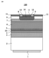
- FIG. 1 is a cross-sectional view showing the device structure of a semiconductor light receiving device according to Embodiment 1.
- FIG. FIG. 3 is a cross-sectional view showing the element structure of a semiconductor light receiving element according to a second embodiment.
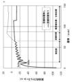
- FIG. 7 is a diagram illustrating the effective stress of the digital alloy structure depending on the presence or absence of a strain relaxation layer in the semiconductor light receiving element according to the second embodiment.
- FIG. 7 is a cross-sectional view showing the element structure of a semiconductor light receiving element according to Embodiment 3.
- 5A is a diagram illustrating the relationship between band gap energies of the semiconductor light receiving element according to Embodiment 3, and FIG. 5A is a diagram when there is no first transition layer, and FIG. 5B is a diagram when there is a first transition layer.
- FIG. 7 is a cross-sectional view showing the element structure of a semiconductor light-receiving element according to Embodiment 4.
- 7B is a diagram illustrating the relationship between bandgap energies of the semiconductor light-receiving device according to Embodiment 4;
- FIG. 7A is a diagram when there is no second transition layer, and
- FIG. 7B is a diagram when there is a second transition layer.
- FIG. 7 is a cross-sectional view showing the element structure of a semiconductor light-receiving element according to Embodiment 5.
- FIG. 3 is a diagram showing an electric field strength distribution in a direction perpendicular to a substrate.
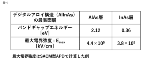
- FIG. 4 is a diagram comparing the maximum electric field strength E MAX when the outermost surface layer of an I-type AlInAs multiplication layer having a digital alloy structure is an AlAs layer and when the outermost surface layer is an InAs layer.
- FIG. 1 is a cross-sectional view showing the device structure of a semiconductor light receiving device 100 according to the first embodiment.
- An SACM type APD is cited as an example of the semiconductor light receiving device 100 according to the first embodiment.
- the semiconductor light-receiving device 100 includes n-type InP substrates having a carrier concentration of 1 to 5 ⁇ 10 18 cm ⁇ 3 and a layer thickness of 0.1 to 0.5 ⁇ m, which are sequentially formed on an n-type InP substrate 2.
- a type AlInAs buffer layer 3 and an i-type AlAs layer (as an example, a layer thickness of 2 ML) and an i-type InAs layer (as an example, a layer thickness of 2 ML) having a layer thickness of 0.05 to 0.2 ⁇ m were laminated multiple times.
- the semiconductor light receiving device 100 further includes a Zn selective diffusion region 10 provided in a part of the n-type InP window layer 8 and the i-type AlInAs window layer 7, and a surface of the Zn selective diffusion region 10.
- the SiNx surface protection film 11 provided on the surface of the n-type InP window layer 8, the n-type electrode 1 provided on the back side of the n-type InP substrate 2, and the surface of the annular p-type InGaAs contact layer 9.
- a p-type electrode 12 provided.
- the semiconductor light-receiving device 100 has the following features: the multiplication layer is an i-type AlInAs multiplication layer 4 having a digital alloy structure, and the i-type AlInAs multiplication layer 4 and the n-type InGaAs light absorption layer 6 are different from each other.
- the feature is that a p-type AlInAs electric field relaxation layer 5 is provided in between.
- the composition ratios of AlInAs and InGaAs constituting each layer are not specified except for AlInAs constituting the multiplication layer 4, but both are lattice matched to the n-type InP substrate 2. It is desirable that the composition ratio is as follows.
- the multiplication layer of the SACM type APD is two monoatomic layers (ML) in thickness, that is, an i-type AlAs layer with a layer thickness of 2ML and an i-type InAs layer with a layer thickness of 2ML.
- the i-type AlInAs multiplier layer 4 which has a digital alloy structure in which are alternately stacked a plurality of times, is taken as an example.
- the thickness of the i-type AlAs layer may be within the range of N times the monoatomic layer (1 ⁇ N ⁇ 20), and the layer thickness of the i-type InAs layer should be within the range of M times the monoatomic layer (1 ⁇ M ⁇ 20).
- the thickness of the i-type AlAs layer is within the range of N times the monoatomic layer (1 ⁇ N ⁇ 5), and the layer thickness of the i-type InAs layer is within the range of M times the monoatomic layer (1 ⁇ M ⁇ 5). It is even more preferable if there is one.
- the i-type AlInAs multiplication layer 4 having a digital alloy structure when the i-type AlAs layer and the i-type InAs layer are alternately laminated multiple times, the number of laminations is preferably in the range of 5 times or more and 300 times or less.
- first semiconductor layer 4a two layers made of different semiconductor materials constituting an AlInAs multiplication layer having a digital alloy structure may be referred to as a first semiconductor layer 4a and a second semiconductor layer 4b.
- the band gap energy Eg 1 of the first semiconductor layer 4a is larger than the band gap energy Eg 2 of the second semiconductor layer 4b, that is, the relationship Eg 1 >Eg 2 holds true.
- the AlAs layer with a band gap energy of 2.12 eV serves as the first semiconductor layer 4a
- the InAs layer with a band gap energy of 0.36 eV serves as the second semiconductor layer 4b.
- n-type AlInAs buffer layer 3 On the surface of the n-type InP substrate 2, there is an n-type AlInAs buffer layer 3 and an i-type AlInAs expansion layer having a digital alloy structure in which i-type AlAs (layer thickness 2 ML) and i-type InAs (layer thickness 2 ML) are alternately laminated multiple times.
- the double layer 4, the p-type AlInAs electric field relaxation layer 5, the n-type InGaAs light absorption layer 6, the i-type AlInAs window layer 7, the n-type InP window layer 8, and the p-type InGaAs contact layer 9 are Crystals are grown sequentially by an epitaxial crystal growth method such as metal organic vapor phase epitaxy (MOVPE) or molecular beam epitaxy (MBE).
- MOVPE metal organic vapor phase epitaxy
- MBE molecular beam epitaxy
- the crystal growth temperature is preferably about 550°C, but may be within the temperature range of 500°C or more and 600°C or less.
- processing of the element region by reactive ion etching, CVD (CVD: Chemical Vapor Deposition), vapor deposition, etc., film formation, and electrode formation are carried out to function as an SACM type APD. Form the necessary element structure.
- a SiOx film is formed on the wafer surface by CVD or the like.
- the SiOx film is an insulating film and functions as a diffusion mask.
- a circular opening is provided in the SiOx film by patterning using a circular pattern mask with a diameter of 40 ⁇ m using photolithography and etching techniques.
- a Zn selective diffusion region 10 is formed in a part of the n-type InP window layer 8 and the i-type AlInAs window layer 7 by a method such as diffusing zinc (Zn) into the semiconductor layer from the opening using the SiOx film as a diffusion mask. form.
- the tip portion of the Zn selective diffusion region 10 inside the semiconductor layer is located in the i-type AlInAs window layer 7 .
- Zn selective diffusion region 10 functions as a p-type conductive region.
- the SiOx film is removed by wet etching or dry etching.
- a SiNx surface protection film 11 is formed on the wafer surface by a CVD method or the like. Subsequently, only the SiNx surface protective film 11 on the surface of the p-type InGaAs contact layer 9 is removed using photolithography and etching techniques. Note that the SiNx surface protection film 11 also has a function as an antireflection film.
- a p-type electrode 12 is formed by depositing a metal material such as Ti/Au on the surface of the p-type InGaAs contact layer 9 by vapor deposition or the like.
- the back side of the n-type InP substrate 2 is ground, and then a metal material such as AuGeNi is deposited by vapor deposition to form the n-type electrode 1.
- a metal material such as AuGeNi is deposited by vapor deposition to form the n-type electrode 1.
- a reverse bias voltage was applied externally so that the n-type electrode 1 provided on the back side of the n-type InP substrate 2 of the SACM type APD was positive and the p-type electrode 12 provided on the front side was negative. hold in condition. Note that the reverse bias voltage is set to a voltage value that sufficiently causes avalanche amplification.
- the light is incident, the light is absorbed in the n-type InGaAs light absorption layer 6 and photocarriers (electron-hole pairs) are generated.
- a reverse bias voltage is applied, the electrons are directed to the n-type electrode 1 side and the holes are They each move to the p-type electrode 12 side.
- the electric field is reduced by the p-type AlInAs electric field relaxation layer 5 so that avalanche amplification occurs when electrons are conducted into the i-type AlInAs multiplication layer 4 having a digital alloy structure. Intensity is controlled.
- the i-type AlInAs multiplication layer 4 having a digital alloy structure electrons are ionized to generate new electron-hole pairs, and the newly generated electrons and holes together cause ionization. is amplified in an avalanche manner. That is, since electrons, which are photocarriers, are multiplied by the avalanche amplification effect within the i-type AlInAs multiplication layer 4, it becomes possible to amplify the received optical signal.
- ⁇ Action of the semiconductor light receiving element In the SACM type APD (semiconductor photodetector), which is an electron multiplier type, when photocarriers generated in the n-type InGaAs light absorption layer are multiplied in the multiplication layer, not only electrons but also holes are multiplied. This causes noise during APD operation.
- the amplitude of the noise is i Ns
- the elementary charge of electrons is q
- the average current value flowing through the avalanche region I
- the band is B
- the avalanche multiplication factor M
- the excess noise factor is F
- the noise component is expressed by the following equation (1).
- the excess noise factor F is expressed by the following equation (2) using the ionization rate ratio k indicating the multiplication rate ratio of holes and electrons.
- the ionization rate ratio k takes a value specific to the material.
- the ionization rate ratio k becomes small, the ratio at which electrons are multiplied is large, so the excess noise coefficient F becomes small, and the noise amplitude i Ns also becomes small. Therefore, since the noise component N that is the denominator in the S/N ratio during APD operation becomes small, the APD can obtain highly sensitive characteristics.
- the ionization rate ratio k is a value specific to the material, it is usually desirable to use a semiconductor material that can grow crystals until the required layer thickness is obtained while maintaining lattice matching with the substrate, and has the lowest ionization rate ratio k possible. , is selected as the semiconductor material constituting the APD.
- binary compound semiconductors AlAs, InAs
- ternary compound semiconductors Al
- the semiconductor material constituting the multiplication layer binary compound semiconductors (AlAs, InAs) or ternary compound semiconductors ( Al
- Al In the case of a multilayer structure formed by crystal growth at a high level, it is possible to improve the electron multiplication factor or suppress the hole multiplication compared to normal semiconductor materials, so the ionization rate ratio k It becomes possible to further reduce the value.
- multiplier layer having a digital alloy structure for example AlInAs, which is a stack of binary compound semiconductor materials such as AlAs and InAs to an atomic layer thickness, as a semiconductor material constituting the multiplier layer of an APD
- SACM type in which the relaxation layer controls the electric field strength applied to the multiplication layer to be larger than the electric field applied to the light absorption layer, it is possible to realize an SACM type APD with low noise and high reception sensitivity.
- Embodiment 1 a case has been described in which AlInAs is used as an example of a semiconductor material constituting the multiplication layer of an SACM type APD.
- the semiconductor material constituting the multiplication layer for example, a semiconductor material capable of crystal growth by combining a group III material and a group V material such as InGaAsP, AlGaInAs, AlAsSb, AlGaAsSb, AlInAsSb, and AlGaInAsSb is used.
- the layer thickness of each layer constituting the digital alloy structure is 2ML.
- any combination of semiconductor materials may be used, not just the one example combination.
- the above-mentioned i-type AlInAs multiplication layer 4 is undoped, the multiplication layer is not limited to undoped. That is, the digital alloy structure itself serving as the multiplication layer may be doped with n-type or p-type impurities.
- a p-type conductive region is formed by Zn diffusion
- atoms other than Zn can serve as p-type impurities as long as they impart p-type conductivity to the n-type InP window layer 8 and the i-type AlInAs window layer 7, such as cadmium (Cd) and beryllium (Be). ) etc. may be used as the p-type dopant.
- the Zn diffusion method may be a solid phase diffusion method using zinc oxide (ZnO), a Zn vapor phase diffusion method using a crystal growth furnace, or the p-type contact layer may be grown by crystal growth.
- a front-illuminated structure in which light to be detected is made to enter the Zn selective diffusion region 10, which is a p-type conductive region, from the p-type electrode 12 side was taken as an example.
- the present disclosure is not limited to a front-illuminated structure, and conversely, a back-illuminated structure in which the n-type electrode 1 is opened in a circular pattern and light is incident from the back side of the n-type InP substrate 2, or an n-type Even with an edge-illuminated structure in which light is incident from the end face of the light absorption layer 6, the same effect as the SACM type APD can be expected.
- the multiplication layer has a digital alloy structure and the electric field relaxation layer is provided between the multiplication layer and the light absorption layer. , it is possible to stably obtain a semiconductor light-receiving element with low noise and high reception sensitivity.
- FIG. 2 is a cross-sectional view showing the element structure of the semiconductor light receiving element 110 according to the second embodiment.
- An SACM type APD is cited as an example of the semiconductor light receiving device 110 according to the second embodiment.
- the semiconductor light receiving device 100 has n-type InP substrates having a carrier concentration of 1 to 5 ⁇ 10 18 cm ⁇ 3 and a layer thickness of 0.1 to 0.5 ⁇ m, which are sequentially formed on an n-type InP substrate 2.
- a type AlInAs buffer layer 3 and an i-type AlAs layer (as an example, a layer thickness of 2 ML) and an i-type InAs layer (as an example, a layer thickness of 2 ML) having a layer thickness of 0.05 to 0.2 ⁇ m were laminated multiple times.
- the i-type AlInAs multiplication layer 4 has a digital alloy structure
- the i-type AlInAs strain relaxation layer 21 has a layer thickness of 10 to 100 nm
- the layer thickness has a carrier concentration of 0.5 to 1 ⁇ 10 18 cm ⁇ 3
- a p-type AlInAs electric field relaxation layer 5 having a thickness of 0.05 to 0.15 ⁇ m
- an n-type InGaAs light absorption layer 6 having a carrier concentration of 1 to 5 ⁇ 10 15 cm ⁇ 3 and a layer thickness of 1 to 1.5 ⁇ m.
- the semiconductor light receiving device 100 further includes a Zn selective diffusion region 10 provided in a part of the n-type InP window layer 8 and the i-type AlInAs window layer 7, and a surface of the Zn selective diffusion region 10.
- the SiNx surface protection film 11 provided on the surface of the n-type InP window layer 8, the n-type electrode 1 provided on the back side of the n-type InP substrate 2, and the surface of the annular p-type InGaAs contact layer 9.
- a p-type electrode 12 provided.
- the semiconductor light-receiving device 110 has the following points: the multiplication layer is an i-type AlInAs multiplication layer 4 having a digital alloy structure, and the i-type AlInAs multiplication layer 4 and the p-type AlInAs electric field relaxation layer 5 are different from each other.
- the feature is that an i-type AlInAs strain relaxation layer 21 is provided in between.
- the method for manufacturing the semiconductor light receiving device 110 according to the second embodiment further includes an i-type AlInAs strain relaxation layer 21 between the i-type AlInAs multiplication layer 4 and the p-type AlInAs electric field relaxation layer 5 during epitaxial crystal growth. Since this embodiment differs from Embodiment 1 only in that crystal growth is performed, a detailed explanation of the manufacturing method will be omitted.
- ⁇ Action of the semiconductor light receiving element 110 according to the second embodiment> In the device structure of the APD, it is necessary to grow a layered structure on the upper surface side of the multiplication layer, from the electric field relaxation layer to the p-type contact layer located at the outermost surface of the semiconductor layer, with a layer thickness of about 2 ⁇ m.
- the crystal quality of the multiplication layer and light absorption layer corresponding to the active layer portion deteriorates during operation as an APD, dark current increases, and noise due to the dark current also increases. Therefore, not only the receiving sensitivity characteristics of the APD deteriorate, but also reliability becomes a concern. Therefore, in order to prevent the occurrence of crystal defects in the vicinity of the multiplication layer, it is important to reduce the stress, or strain, in the stacked structure itself as much as possible in order to realize a high-performance and highly reliable APD. .
- the multiplier layer which has a digital alloy structure, is made by laminating binary or ternary compound semiconductor materials that are lattice-mismatched and have a lattice constant that does not match that of the substrate, so they are laminated while alternating compressive strain and tensile strain. It turns out.
- the effective stress ⁇ when dislocation occurs can be calculated using the mechanical equilibrium model disclosed in Non-Patent Document 3 mentioned above. In other words, as disclosed in FIG.
- the laminated structure is configured such that the effective stress ⁇ becomes zero or less, and the materials and layer thicknesses used when crystal-growing an element structure including a digital alloy structure are By controlling the order, it is possible to achieve high-quality crystal growth without generating dislocations, that is, without generating crystal defects, making it possible to obtain an APD with excellent device characteristics.
- the effective stress ⁇ in a structure in which compressive strain and tensile strain are alternately stacked, such as a multi-quantum well structure is expressed by the following equation (3) and each parameter.
- FIG. 3 shows the results of calculating the effective stress value based on equation (3) for both cases. Note that Non-Patent Document 3 was referred to for the calculation parameters.
- the InAs layer constituting the digital alloy structure of the second embodiment was used as a compressive strain layer, and the AlAs layer was used as a tensile strain layer, and the physical property values of the respective compound semiconductor materials were used.
- the effective stress ⁇ when crystal-growing an AlInAs multiplication layer having a digital alloy structure is such that the effective stress ⁇ applied to the entire device structure increases at once because the InAs layer has a high compressive strain.
- the AlAs layer which is crystal-grown immediately after the InAs layer, has tensile strain that acts in the opposite direction to the compressive strain, it acts in a direction that alleviates the effective stress ⁇ .
- the effective stress ⁇ applied to the entire device structure gradually increases as InAs layers and AlAs layers are alternately stacked.
- the stress accumulated during the formation of the AlInAs multiplication layer having a digital alloy structure will be inherited as is. If a strain relaxation layer is not applied, when crystal growth is performed for a device structure that requires a layer thickness of about 2 ⁇ m, the effective stress ⁇ exceeds zero, resulting in dislocations and poor crystal quality. The calculation results show that it is easy.
- an i-type AlInAs strain relaxation layer 21 is provided between the i-type AlInAs multiplication layer 4 and the p-type AlInAs electric field relaxation layer 5.
- a strain relaxation layer When such a strain relaxation layer is inserted, the crystal growth of the i-type AlInAs multiplication layer 4 having a digital alloy structure is reduced due to the strain relaxation effect of the strain relaxation layer during crystal growth of the strain relaxation layer and the light absorption layer. It becomes possible to reduce the effective stress ⁇ that has increased during this time.
- by inserting the strain relaxation layer it is possible to fabricate an SACM type APD consisting of a high quality semiconductor crystal growth layer that does not generate dislocations during crystal growth of the entire device structure.
- an i-type AlInAs layer is used as an example of the strain relaxation layer.
- the semiconductor material is not limited to AlInAs as long as the semiconductor material is lattice matched to the substrate used.
- the strain relaxation layer may not be undoped as described above, but may be doped with an impurity so as to have p-type or n-type conductivity, for example.
- the effective stress ⁇ of the entire device structure can be controlled so as not to exceed zero, there is no problem even if the strain relaxation layer itself is strained. Further, even if the strain relaxation layer itself is strained, even better effects can be achieved if the strain of the entire device structure is controlled so as to be opposite to the average strain of the digital alloy structure.
- FIG. 4 is a cross-sectional view showing the element structure of the semiconductor light receiving element 120 according to the third embodiment.
- An SACM type APD is cited as an example of the semiconductor light receiving element 120 according to the third embodiment.
- the semiconductor light-receiving device 120 has n-type InP substrates having a carrier concentration of 1 to 5 ⁇ 10 18 cm ⁇ 3 and a layer thickness of 0.1 to 0.5 ⁇ m, which are sequentially formed on an n-type InP substrate 2.
- a type AlInAs buffer layer 3 and an i-type AlAs layer (as an example, a layer thickness of 2 ML) and an i-type InAs layer (as an example, a layer thickness of 2 ML) having a layer thickness of 0.05 to 0.2 ⁇ m were laminated multiple times.
- the semiconductor light receiving element 120 further includes a Zn selective diffusion region 10 provided in a part of the n-type InP window layer 8 and the i-type AlInAs window layer 7, and a surface of the Zn selective diffusion region 10.
- the SiNx surface protection film 11 provided on the surface of the n-type InP window layer 8, the n-type electrode 1 provided on the back side of the n-type InP substrate 2, and the surface of the annular p-type InGaAs contact layer 9.
- a p-type electrode 12 provided.
- the semiconductor light-receiving device 120 has the following features: the multiplication layer is an i-type AlInAs multiplication layer 4 having a digital alloy structure, and the i-type AlInAs multiplication layer 4 and the p-type AlInAs electric field relaxation layer 5 are different from each other.
- a feature is that an i-type Al x Ga y In 1-xy As first transition layer 22 with a layer thickness of 15 nm is provided in between.
- an i-type AlInAs multiplier layer 4 having a digital alloy structure and a p-type AlInAs electric field relaxation layer 5 are further provided with an i-type AlInAs multiplier layer 4 having a digital alloy structure.
- the only difference from Embodiment 1 is that the first transition layer 22 of x Ga y In 1-x-y As is grown as a crystal, so a detailed explanation of the manufacturing method will be omitted.
- Photocarriers that is, electrons and holes generated when light is incident on the APD, move in a direction opposite to their respective polarities within the light absorption layer to which a reverse bias is applied. Electrons generated within the light absorption layer are conducted into the multiplication layer, pass through the electric field relaxation layer, and then reach the multiplication layer, where an avalanche amplification effect occurs within the multiplication layer.
- the band structure of the multiplication layer itself changes depending on the semiconductor materials combined as the first semiconductor layer 4a and the second semiconductor layer 4b forming the digital alloy structure. Since the conduction band is located higher than the electric field relaxation layer 5, an electron barrier ⁇ Ec may occur when electrons are conducted to the multiplication layer 4 having a digital alloy structure.
- FIG. 5 is a diagram illustrating the relationship between the band gap energies of each layer of the semiconductor light-receiving device 120 according to the third embodiment, in which FIG. 5A shows a case where the first transition layer 22 is not present, and FIG. 5B shows a case where the first transition layer 22 is present. It is a figure showing each case.
- FIG. 5A when the electric field relaxation layer 5 and the multiplication layer 4 having a digital alloy structure are in contact with each other, electrons cannot move from the electric field relaxation layer 5 to the multiplication layer 4 having a digital alloy structure. , it was necessary to overcome the electron barrier ⁇ Ec.
- the semiconductor light receiving element 120 is formed between the multiplication layer 4 having a digital alloy structure and the electric field relaxation layer 5, and the bandgap energy Eg of the multiplication layer 4 having a digital alloy structure and
- the first transition layer 22 has a band gap energy Eg m between the band gap energy Eg b of the electric field relaxation layer 5 and relieves strain in the multiplication layer 4 having a digital alloy structure.
- an i-type Al x Ga y In 1-xy As layer is used as an example of the first transition layer 22.
- the semiconductor material has a bandgap energy value between the bandgap energy Eg of the multiplication layer 4 having a digital alloy structure and the bandgap energy Egb of the electric field relaxation layer 5, Al x shown in the above example can be used. It is not limited to the Ga y In 1-xy As layer, but may be other semiconductor materials. Furthermore, control becomes easier if the first transition layer 22 is configured by combining semiconductor layers having the same composition as the layers constituting the digital alloy structure.
- the digital alloy structure is made of Al, In, and As as in the above example, if the first transition layer 22 is also made of Al, In, and As, Control becomes easier.
- the first transition layer 22 may not be undoped, but may be doped with an impurity so as to have, for example, p-type or n-type conductivity.
- FIG. 6 is a cross-sectional view showing the element structure of the semiconductor light receiving element 130 according to the fourth embodiment.
- An SACM type APD is cited as an example of the semiconductor light receiving element 130 according to the fourth embodiment.
- the semiconductor light-receiving device 130 has n-type InP substrates 2 with carrier concentrations of 1 to 5 ⁇ 10 18 cm ⁇ 3 and layer thicknesses of 0.1 to 0.5 ⁇ m, which are sequentially formed on an n-type InP substrate 2.
- an i-type AlInAs multiplication layer 4 made of a digital alloy structure in which an i-type AlAs layer (layer thickness 2 ML as an example) and an i-type InAs layer (layer thickness 2 ML as an example) are alternately laminated multiple times.
- a p-type AlInAs electric field relaxation layer 5 with a carrier concentration of 0.5 to 1 ⁇ 10 18 cm ⁇ 3 and a layer thickness of 0.05 to 0.15 ⁇ m, and a carrier concentration of 1 to 5 ⁇ 10 15 cm ⁇ 3
- An n-type InGaAs light absorption layer 6 with a layer thickness of 1 to 1.5 ⁇ m
- an i-type AlInAs window layer 7 with a layer thickness of 0.05 to 1 ⁇ m, and a carrier concentration of 0.1 to 5 ⁇ 10 15 cm ⁇ 3 and a layer thickness of 0.5 to 1 ⁇ m, and a circle having a carrier concentration of 1 to 5 ⁇ 10 18 cm ⁇ 3 and a layer thickness of 0.1 to 0.5 ⁇ m.
- It is composed of a p-type InGaAs contact layer 9 having an annular shape.
- the semiconductor light receiving element 130 further includes a Zn selective diffusion region 10 provided in a part of the n-type InP window layer 8 and the i-type AlInAs window layer 7, and a surface of the Zn selective diffusion region 10.
- the SiNx surface protection film 11 provided on the surface of the n-type InP window layer 8, the n-type electrode 1 provided on the back side of the n-type InP substrate 2, and the surface of the annular p-type InGaAs contact layer 9.
- a p-type electrode 12 provided.
- the semiconductor light-receiving device 130 has an i-type AlInAs multiplication layer 4 having a digital alloy structure as the multiplication layer, and a difference between the n-type AlInAs buffer layer 3 and the i-type AlInAs multiplication layer 4.
- the structure is characterized in that an i-type Al x Ga y In 1-xy As second transition layer 23 with a layer thickness of 15 nm is provided.
- the method for manufacturing the semiconductor light-receiving device 130 according to the fourth embodiment further includes i-type Al x Ga y In 1- between the n-type AlInAs buffer layer 3 and the i-type AlInAs multiplication layer 4 during epitaxial crystal growth.
- the only difference from Embodiment 1 is that the xy As second transition layer 23 is grown as a crystal, so a detailed explanation of the manufacturing method will be omitted.
- the conduction band is lower than the n-type AlInAs buffer layer 3 on the substrate side or the electric field relaxation layer 5, and may become a barrier for electrons. There is.
- the n-type AlInAs buffer layer 3 and the n-type InP substrate 2 have to pass before the electrons amplified in the i-type AlInAs multiplication layer 4 having a digital alloy structure are conducted as carriers to the p-type InGaAs contact layer 9. Energy is required to overcome the electron barrier that exists between the two, which may become an obstacle to high-speed operation of the SACM type APD, especially under low voltage.
- the SACM type APD which is an example of the semiconductor light receiving device 130 according to the fourth embodiment, has a layer between an i-type AlInAs multiplication layer 4 and an n-type AlInAs buffer layer 3 having a digital alloy structure.
- FIG. 7A and 7B are diagrams illustrating the relationship between the band gap energies of each layer in the semiconductor light-receiving device according to the fourth embodiment, in which FIG. 7A shows a case where there is no second transition layer 23, and FIG. 7B shows a case where there is a second transition layer 23. It is a figure showing each case.
- FIG. 7A when the multiplication layer 4 having a digital alloy structure and the buffer layer 3 are in contact with each other, an electron barrier is required for electrons to move from the multiplication layer 4 having a digital alloy structure to the buffer layer 3. It is necessary to exceed ⁇ Ec'.
- the second transition layer 23 when the second transition layer 23 is provided between the multiplication layer 4 having a digital alloy structure and the buffer layer 3, the second transition layer 23 is formed between the multiplication layer 4 having a digital alloy structure and the buffer layer 3.
- the electron barrier ⁇ Ec3 which is smaller than the electron barrier ⁇ Ec'. It is sufficient if it exceeds ⁇ Ec4.
- the insertion of the above-mentioned i-type Al x Ga y In 1-x-y As second transition layer 23 has the same effect of reducing the stress accumulated in the i-type AlInAs multiplication layer 4 having a digital alloy structure. to play.
- an i-type Al x Ga y In 1-xy As layer is used as an example of the semiconductor material constituting the second transition layer 23, but the band gap energy Eg n of the second transition layer 23, The same applies if the semiconductor material satisfies the relationship Eg> Egn > Egs between the bandgap energy Eg of the i-type AlInAs multiplication layer 4 and the bandgap energy Egs of the n-type AlInAs buffer layer 3 . Applicable. Further, control becomes easier if the second transition layer 23 is configured by combining layers having the same composition as the layers constituting the digital alloy structure. Further, the second transition layer 23 may not be undoped as in the example, but may be doped with an impurity so as to have, for example, a p-type or n-type conductivity type.
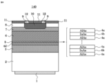
- FIG. 8 is a cross-sectional view showing the element structure of the semiconductor light receiving element 140 according to the fifth embodiment.
- An SACM type APD is cited as an example of the semiconductor light receiving element 140 according to the first embodiment.
- each layer of the semiconductor light-receiving device 140 according to the fifth embodiment is basically the same as the structure of each layer of the semiconductor light-receiving device 100 according to the first embodiment, but an i-type AlInAs multiplication device having a digital alloy structure is used.
- the detailed structure of the layer 4d is different. Therefore, only the structure of the i-type AlInAs multiplication layer 4d having a digital alloy structure will be described below.
- the i-type AlInAs multiplication layer 4d having a digital alloy structure has a layer thickness of 0.05 to 0.2 ⁇ m, including an i-type AlAs layer (layer thickness 2ML as an example) and an i-type InAs layer (layer thickness 2ML as an example).
- the last layer laminated as the i-type AlInAs multiplication layer 4d having a digital alloy structure that is, the outermost layer is the i-type AlInAs layer. becomes.
- This configuration is applied to the i-type AlAs layer and the i-type InAs layer, which are the two layers constituting the i-type AlInAs multiplication layer 4d having a digital alloy structure, whichever has the larger band gap energy. This is because the i-type AlAs layer is the outermost layer.
- the band gap energy Eg 1 of the first semiconductor layer 4a is larger than the band gap energy Eg 2 of the second semiconductor layer 4b, that is, Eg 1 >Eg 2 .
- the AlAs layer with a band gap energy Eg 1 of 2.12 eV serves as the first semiconductor layer 4a
- the InAs layer with a band gap energy Eg 2 of 0.36 eV serves as the second semiconductor layer 4b.
- the i-type AlInAs multiplication layer 4d having a digital alloy structure has a layer thickness of 0.05 to 0.2 ⁇ m, and is made by laminating the first semiconductor layer 4a and the second semiconductor layer 4b alternately multiple times. , the last layer laminated as the i-type AlInAs multiplication layer 4d having a digital alloy structure, that is, the layer on the outermost surface side becomes the first semiconductor layer 4a. That is, the layer facing the p-type AlInAs electric field relaxation layer 5 in the i-type AlInAs multiplication layer 4d having a digital alloy structure becomes the first semiconductor layer 4a.
- the method for manufacturing the semiconductor light-receiving device 140 according to the fifth embodiment is almost the same as the method for manufacturing the semiconductor light-receiving device 100 according to the first embodiment, so a detailed explanation of the manufacturing method will be omitted.
- FIG. 9 shows the electric field intensity distribution in the direction perpendicular to the n-type InP substrate 2.
- SACM type APD the electric field strength applied to the i-type AlInAs multiplication layer 4d having a digital alloy structure is increased so that carriers are multiplied by avalanche.
- a p-type AlInAs electric field relaxation layer 5 is used to reduce the electric field strength in the n-type InGaAs light absorption layer 6. Control.
- the maximum electric field strength E max of the i-type AlInAs multiplication layer 4d has a relationship expressed by the following equation (4) with the band gap energy Eg of the i-type AlInAs multiplication layer 4d having a digital alloy structure. .
- the larger the band gap energy Eg of the i-type AlInAs multiplication layer 4d having a digital alloy structure is, the larger the maximum electric field strength E max is, so that the voltage that can be controlled as an SACM type APD can be increased.
- the i-type AlInAs multiplication layer 4d having a digital alloy structure is composed of a binary compound semiconductor material of an InAs layer and an AlAs layer
- the AlAs layer having a larger band gap energy is set as the outermost layer of the digital alloy structure. By doing so, the maximum electric field strength E max in the entire element can be increased.
- FIG. 10 compares the maximum electric field strength E max when the outermost surface layer of the i-type AlInAs multiplication layer 4d having a digital alloy structure is an AlAs layer and when the outermost surface layer is an InAs layer. From FIG. 10, the maximum electric field strength E max when the outermost surface layer is an AlAs layer is 4.4 ⁇ 10 5 kV/cm, whereas the maximum electric field strength E max when the outermost surface layer is an InAs layer. max is 3.8 ⁇ 10 5 kV/cm, and it can be seen that a larger maximum electric field strength E max can be obtained when the outermost surface layer is an AlAs layer.
- the resistance to the electric field becomes stronger even when a local electric field occurs at the interface between the electric field relaxation layer and the multiplication layer. Furthermore, it becomes possible to reduce the electron barrier ⁇ Ec that inhibits carrier conduction.
- Embodiment 5 as an example, a configuration in which the AlAs layer in the i-type AlInAs multiplication layer 4d having a digital alloy structure is the outermost layer has been described.
- the same effect can be obtained by making the semiconductor layer with a larger band gap energy as the outermost layer among the two types of semiconductor layers constituting the multiplication layer having a digital alloy structure.
- the same effect can be achieved even if the semiconductor material is not limited as long as the magnitude relationship of band gap energy is satisfied.
- the two types of semiconductor layers constituting the multiplication layer having a digital alloy structure are not limited to binary compound semiconductor materials as shown in the above example, but may be, for example, Al x In 1-x As. It may be a ternary compound semiconductor material such as Al x Ga y In 1-xy As, or a quaternary compound semiconductor material such as Al x Ga y In 1-xy As. Furthermore, the multiplication layer is not undoped as shown in the example, but may be doped with an impurity so as to have p-type or n-type conductivity, for example.
- the semiconductor layer having a larger band gap energy is used as the outermost layer. Therefore, the maximum electric field strength within the multiplication layer having the digital alloy structure increases, and the control range of the operable voltage can be widened, resulting in the effect that a semiconductor light-receiving element capable of high-speed operation can be obtained.
Landscapes
- Light Receiving Elements (AREA)
Abstract
Description
半導体基板と、
前記半導体基板上に形成され、単原子層のN倍(1≦N≦20)の層厚からなる第1半導体層、及び単原子層のM倍(1≦M≦20)の層厚からなり前記第1半導体層よりもバンドギャップエネルギーが小さい第2半導体層が交互に複数回積層されたデジタルアロイ構造からなり、フォトキャリアを増幅させる増倍層と、
前記増倍層上に形成され、入射光を吸収して前記フォトキャリアを生成する光吸収層と、
前記増倍層と前記光吸収層との間に形成された電界緩和層と、を備える。
n型InP基板上に、n型AlInAsバッファ層と、単原子層のN倍(1≦N≦20)の層厚からなるAlAs層、及び単原子層のM倍(1≦M≦20)の層厚からなるInAs層が交互に複数回積層されたデジタルアロイ構造からなるAlInAs増倍層と、p型AlInAs電界緩和層と、n型InGaAs光吸収層と、i型AlInAs窓層と、n型InP窓層と、p型InGaAsコンタクト層と、を順次エピタキシャル結晶成長する工程と、
前記n型InP窓層及びi型AlInAs窓層の一部にZn選択拡散領域を形成する工程と、を備える。
<実施の形態1に係る半導体受光素子100の素子構造>
図1は、実施の形態1に係る半導体受光素子100の素子構造を表す断面図である。実施の形態1に係る半導体受光素子100の一例として、SACM型APDを挙げている。
まず、実施の形態1に係る半導体受光素子100の一例であるSACM型APDの製造方法を、以下に説明する。
以上が、実施の形態1に係る半導体受光素子100の一例であるSACM型APDの製造方法である。
上述の製造方法によって作製された実施の形態1に係る半導体受光素子100の一例であるSACM型APDの動作を、以下に説明する。
電子増倍型であるSACM型APD(半導体受光素子)では、n型InGaAs光吸収層内で生成されたフォトキャリアが増倍層内で増倍される際に、電子だけでなくホールも増倍されてAPD動作時の雑音要因となる。雑音の振幅をiNs、電子の素電荷をq、アバランシェ領域を流れる平均電流値をI、帯域をB、アバランシェ増倍率をM、過剰雑音係数をFとした場合、受信感度の性能を低下させる雑音成分は、以下の式(1)で表される。

過剰雑音係数Fは、ホールと電子の増倍率比を示すイオン化率比kを用いて、以下の式(2)で表される。
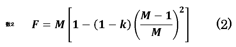
以上、実施の形態1に係る半導体受光素子及び半導体受光素子の製造方法によれば、増倍層をデジタルアロイ構造とし、かつ増倍層と光吸収層との間に電界緩和層を設けたので、低雑音であり、かつ受信感度の高い半導体受光素子が安定に得られるという効果を奏する。
<実施の形態2に係る半導体受光素子110の素子構造>
図2は、実施の形態2に係る半導体受光素子110の素子構造を表す断面図である。実施の形態2に係る半導体受光素子110の一例として、SACM型APDを挙げている。
APDの素子構造では増倍層の上面側に電界緩和層から半導体層としての最表面に位置するp型コンタクト層まで、層厚として2μm程度の積層構造を結晶成長する必要がある。特に、APDとしての動作時に、活性層部分に相当する増倍層及び光吸収層は、結晶品質が悪化すると暗電流が増加し、暗電流に起因する雑音も増加する。したがって、APDの受信感度特性が悪化するほか、信頼性への懸念点ともなる。よって、増倍層の近傍での結晶欠陥の発生を防止するため、積層構造自体のストレス、つまり歪みを可能な限り低減することが、高性能かつ高信頼性のAPDを実現するに当たって重要となる。

λ : 転位線とバーガースペクトルのなす角
ν : ポアソン比
μx : 圧縮歪層のせん断係数
μy : 引張歪層のせん断係数
μxy : 繰り返し積層部分の平均せん断係数
b : バーガースペクトル
cosθ : 転位線とバーガースペクトルのなす角
β : コア係数(core parameter)
x : 圧縮歪層の歪量
h : 圧縮歪層の層厚
y : 引張歪層の歪量
H : 引張歪層の層厚
Z : 歪緩和層の層厚
N : 圧縮歪層の層数
L : Nh+(N-1)Hの計算値
以上、実施の形態2に係る半導体受光素子によれば、AlInAs増倍層とAlInAs電界緩和層との間にAlInAs歪緩和層を設けたので、デジタルアロイ構造からなるi型AlInAs増倍層の形成によって発生するストレスを緩和できるので、高性能でかつ信頼性の高い半導体受光素子が得られるという効果を奏する。
<実施の形態3に係る半導体受光素子120の素子構造>
図4は、実施の形態3に係る半導体受光素子120の素子構造を表す断面図である。実施の形態3に係る半導体受光素子120の一例として、SACM型APDを挙げている。
APDに光が入射して発生したフォトキャリア、つまり電子及びホールは、逆バイアスに印加された光吸収層内でそれぞれの極性とは逆の方向に移動する。光吸収層内で発生した電子は増倍層内に向けて伝導し、電界緩和層を通過した後に増倍層に到達して、増倍層内でアバランシェ増幅作用が発生する。デジタルアロイ構造からなる増倍層4を適用する場合、デジタルアロイ構造を構成する第1半導体層4a及び第2半導体層4bとして組み合わせる半導体材料によっては、増倍層自体のバンド構造が変化して、電界緩和層5よりも伝導帯の位置が高くなるため、電子がデジタルアロイ構造からなる増倍層4へと伝導する際の電子障壁ΔEcとなる場合がある。
以上、実施の形態3に係る半導体受光素子によれば、デジタルアロイ構造からなるi型AlInAs増倍層とp型AlInAs電界緩和層との間にi型AlxGayIn1-x-yAs第1遷移層を設けたので、デジタルアロイ構造からなるi型AlInAs増倍層と電界緩和層との間に発生する電子障壁が実効的に減少するので、キャリア伝導性が改善するため、高速動作が可能な半導体受光素子が得られるという効果を奏する。
<実施の形態4に係る半導体受光素子130の素子構造>
図6は、実施の形態4に係る半導体受光素子130の素子構造を表す断面図である。実施の形態4に係る半導体受光素子130の一例として、SACM型APDを挙げている。
実施の形態3に係る半導体受光素子120では、光がAPDに入射し、光吸収層で発生したフォトキャリアの電子が電界緩和層を通過して増倍層に到達する際の電子障壁ΔEcについての改善効果を示した。しかしながら、デジタルアロイ構造からなるi型AlInAs増倍層4自体のバンド構造では、基板側のn型AlInAsバッファ層3、あるいは電界緩和層5よりも伝導帯の位置が低く、電子にとって障壁となる場合がある。
以上、実施の形態4に係る半導体受光素子によれば、デジタルアロイ構造からなる増倍層とn型バッファ層との間に第2遷移層を設けたので、デジタルアロイ構造からなる増倍層とn型バッファ層との間に発生する電子障壁が減少する結果、キャリア伝導性が改善するため、高速動作が可能な半導体受光素子が得られるという効果を奏する。
<実施の形態5に係る半導体受光素子140の素子構造>
図8は、実施の形態5に係る半導体受光素子140の素子構造を表す断面図である。実施の形態1に係る半導体受光素子140の一例として、SACM型APDを挙げている。
デジタルアロイ構造からなるi型AlInAs増倍層4dを構成する、半導体材料がそれぞれ異なる2層が、第1半導体層4a及び第2半導体層4bであるとする。ここで、第1半導体層4aのバンドギャップエネルギーEg1は、第2半導体層4bのバンドギャップエネルギーEg2よりも大きい、つまり、Eg1>Eg2、とする。なお、上述の一例では、バンドギャップエネルギーEg1が2.12eVであるAlAs層が第1半導体層4a、バンドギャップエネルギーEg2が0.36eVであるInAs層が第2半導体層4bとなる。
n型InP基板2に垂直方向の電界強度分布を図9に示す。SACM型APDではキャリアがアバランシェ増倍されるように、デジタルアロイ構造からなるi型AlInAs増倍層4dにかかる電界強度を大きくする。一方、n型InGaAs光吸収層6においてはキャリアが増倍しないようにするため、n型InGaAs光吸収層6の電界強度を低減させるために、p型AlInAs電界緩和層5を用いて電界強度を制御する。この場合、i型AlInAs増倍層4dの最大電界強度Emaxは、デジタルアロイ構造からなるi型AlInAs増倍層4dのバンドギャップエネルギーEgと、以下の式(4)に表される関係にある。

以上、実施の形態5に係る半導体受光素子によれば、デジタルアロイ構造からなる増倍層を構成する2種類の半導体層の中で、バンドギャップエネルギーが大きい方の半導体層を最表面層としたので、デジタルアロイ構造からなる増倍層内における最大電界強度が大きくなり、動作可能な電圧の制御幅を広げることができるため、高速動作が可能な半導体受光素子が得られるという効果を奏する。
Claims (18)
- 半導体基板と、
前記半導体基板上に形成され、単原子層のN倍(1≦N≦20)の層厚からなる第1半導体層、及び単原子層のM倍(1≦M≦20)の層厚からなり前記第1半導体層よりもバンドギャップエネルギーが小さい第2半導体層が交互に複数回積層されたデジタルアロイ構造からなり、フォトキャリアを増幅させる増倍層と、
前記増倍層上に形成され、入射光を吸収して前記フォトキャリアを生成する光吸収層と、
前記増倍層と前記光吸収層との間に形成された電界緩和層と、
を備える半導体受光素子。 - 前記第1半導体層の層厚が単原子層のN倍(1≦N≦5)であり、前記第2半導体層の層厚が単原子層のM倍(1≦M≦5)の層厚であることを特徴とする請求項1に記載の半導体受光素子。
- 前記第1半導体層と前記第2半導体層とを交互に積層する積層回数が5回以上300回以下であることを特徴とする請求項1または2に記載の半導体受光素子。
- 前記第1半導体層及び前記第2半導体層は、それぞれAlAs層及びInAs層であることを特徴とする請求項1から3のいずれか1項に記載の半導体受光素子。
- 前記光吸収層は、InGaAsによって構成されることを特徴とする請求項1から4のいずれか1項に記載の半導体受光素子。
- 前記増倍層と前記電界緩和層との間に形成され、前記増倍層の歪を緩和する歪緩和層をさらに備えることを特徴とする請求項1から5のいずれか1項に記載の半導体受光素子。
- 前記歪緩和層は、前記増倍層を構成する半導体材料と同一の組成の半導体材料からなることを特徴とする請求項6に記載の半導体受光素子。
- 前記歪緩和層は、AlInAsによって構成されることを特徴とする請求項6または7に記載の半導体受光素子。
- 前記増倍層と前記電界緩和層との間に形成され、前記増倍層のバンドギャップエネルギーと前記電界緩和層のバンドギャップエネルギーの間のバンドギャップエネルギー値を有し、前記増倍層の歪を緩和する第1遷移層をさらに備えることを特徴とする請求項1から5のいずれか1項に記載の半導体受光素子。
- 前記第1遷移層は、AlGaInAsによって構成されることを特徴とする請求項9に記載の半導体受光素子。
- 前記半導体基板と前記増倍層との間に形成されたバッファ層と、
前記増倍層と前記バッファ層との間に、前記増倍層のバンドギャップエネルギーと前記バッファ層のバンドギャップエネルギーの間のバンドギャップエネルギー値を有し、前記増倍層の歪を緩和する第2遷移層と、をさらに備えることを特徴とする請求項1から5のいずれか1項に記載の半導体受光素子。 - 前記第2遷移層は、AlGaInAsによって構成されることを特徴とする請求項11に記載の半導体受光素子。
- 前記増倍層において前記電界緩和層に対向する層は、前記第1半導体層であることを特徴とする請求項1から5のいずれか1項に記載の半導体受光素子。
- n型InP基板上に、n型AlInAsバッファ層と、単原子層のN倍(1≦N≦20)の層厚からなるAlAs層、及び単原子層のM倍(1≦M≦20)の層厚からなるInAs層が交互に複数回積層されたデジタルアロイ構造からなるAlInAs増倍層と、p型AlInAs電界緩和層と、n型InGaAs光吸収層と、i型AlInAs窓層と、n型InP窓層と、p型InGaAsコンタクト層と、を順次エピタキシャル結晶成長する工程と、
前記n型InP窓層及びi型AlInAs窓層の一部にZn選択拡散領域を形成する工程と、
を備える半導体受光素子の製造方法。 - 前記エピタキシャル結晶成長はMOVPE法またはMBE法によって行われることを特徴とする請求項14に記載の半導体受光素子の製造方法。
- 前記エピタキシャル結晶成長はMOVPE法によって行われ、結晶成長温度は500℃以上600℃以下の範囲内であることを特徴とする請求項14に記載の半導体受光素子の製造方法。
- 前記AlAs層の層厚が単原子層のN倍(1≦N≦5)であり、前記InAs層の層厚が単原子層のM倍(1≦M≦5)の層厚であることを特徴とする請求項14から16のいずれか1項に記載の半導体受光素子の製造方法。
- 前記AlAs層と前記InAs層とを交互に積層する積層回数が5回以上300回以下であることを特徴とする請求項14から17のいずれか1項に記載の半導体受光素子の製造方法。
Priority Applications (4)
| Application Number | Priority Date | Filing Date | Title |
|---|---|---|---|
| CN202280097208.2A CN119404612A (zh) | 2022-06-22 | 2022-06-22 | 半导体受光元件及半导体受光元件的制造方法 |
| JP2022568606A JP7224560B1 (ja) | 2022-06-22 | 2022-06-22 | 半導体受光素子及び半導体受光素子の製造方法 |
| US18/849,222 US20250204059A1 (en) | 2022-06-22 | 2022-06-22 | Semiconductor light-receiving device and method for manufacturing same |
| PCT/JP2022/024800 WO2023248367A1 (ja) | 2022-06-22 | 2022-06-22 | 半導体受光素子及び半導体受光素子の製造方法 |
Applications Claiming Priority (1)
| Application Number | Priority Date | Filing Date | Title |
|---|---|---|---|
| PCT/JP2022/024800 WO2023248367A1 (ja) | 2022-06-22 | 2022-06-22 | 半導体受光素子及び半導体受光素子の製造方法 |
Publications (1)
| Publication Number | Publication Date |
|---|---|
| WO2023248367A1 true WO2023248367A1 (ja) | 2023-12-28 |
Family
ID=85226227
Family Applications (1)
| Application Number | Title | Priority Date | Filing Date |
|---|---|---|---|
| PCT/JP2022/024800 Ceased WO2023248367A1 (ja) | 2022-06-22 | 2022-06-22 | 半導体受光素子及び半導体受光素子の製造方法 |
Country Status (4)
| Country | Link |
|---|---|
| US (1) | US20250204059A1 (ja) |
| JP (1) | JP7224560B1 (ja) |
| CN (1) | CN119404612A (ja) |
| WO (1) | WO2023248367A1 (ja) |
Cited By (1)
| Publication number | Priority date | Publication date | Assignee | Title |
|---|---|---|---|---|
| JP7615412B1 (ja) * | 2024-03-26 | 2025-01-16 | 三菱電機株式会社 | 半導体受光素子、半導体受光素子の製造方法、光回線終端装置、多値強度変調送受信装置、デジタルコヒーレント受信装置、光ファイバ無線システム、spadセンサーシステム、及びライダー装置 |
Families Citing this family (5)
| Publication number | Priority date | Publication date | Assignee | Title |
|---|---|---|---|---|
| WO2024214172A1 (ja) * | 2023-04-11 | 2024-10-17 | 三菱電機株式会社 | 半導体受光素子及び半導体受光素子の製造方法 |
| WO2025079193A1 (ja) * | 2023-10-12 | 2025-04-17 | 三菱電機株式会社 | 半導体受光素子、光回線終端装置、多値強度変調送受信装置、デジタルコヒーレント受信装置、光ファイバ無線システム、spadセンサーシステム、及びライダー装置 |
| JP7511793B1 (ja) * | 2023-11-13 | 2024-07-05 | 三菱電機株式会社 | 半導体受光素子、光回線終端装置、多値強度変調送受信装置、デジタルコヒーレント受信装置、光ファイバ無線システム、spadセンサーシステム、及びライダー装置 |
| JP7661633B1 (ja) * | 2024-04-03 | 2025-04-14 | 三菱電機株式会社 | 半導体受光素子、光回線終端装置、多値強度変調送受信装置、デジタルコヒーレント受信装置、光ファイバ無線システム、spadセンサーシステム、及びライダー装置 |
| CN121619970A (zh) * | 2026-01-29 | 2026-03-06 | 国科大杭州高等研究院 | 雪崩光电探测器及其制备方法 |
Citations (6)
| Publication number | Priority date | Publication date | Assignee | Title |
|---|---|---|---|---|
| JPH07335934A (ja) * | 1994-06-03 | 1995-12-22 | Mitsubishi Electric Corp | 光半導体素子,及びその製造方法 |
| WO2006123410A1 (ja) * | 2005-05-18 | 2006-11-23 | Mitsubishi Denki Kabushiki Kaisha | アバランシェフォトダイオード |
| JP2014099467A (ja) * | 2012-11-13 | 2014-05-29 | Mitsubishi Electric Corp | アバランシェフォトダイオードおよびその製造方法 |
| US20170244002A1 (en) * | 2016-02-22 | 2017-08-24 | University Of Virginia Patent Foundation | AlInAsSb Avalanche Photodiode and Related Method thereof |
| JP2018152369A (ja) * | 2017-03-09 | 2018-09-27 | 三菱電機株式会社 | 裏面入射型受光素子およびその製造方法 |
| JP7024918B1 (ja) * | 2021-01-21 | 2022-02-24 | 三菱電機株式会社 | アバランシェフォトダイオード |
-
2022
- 2022-06-22 CN CN202280097208.2A patent/CN119404612A/zh active Pending
- 2022-06-22 WO PCT/JP2022/024800 patent/WO2023248367A1/ja not_active Ceased
- 2022-06-22 JP JP2022568606A patent/JP7224560B1/ja active Active
- 2022-06-22 US US18/849,222 patent/US20250204059A1/en active Pending
Patent Citations (6)
| Publication number | Priority date | Publication date | Assignee | Title |
|---|---|---|---|---|
| JPH07335934A (ja) * | 1994-06-03 | 1995-12-22 | Mitsubishi Electric Corp | 光半導体素子,及びその製造方法 |
| WO2006123410A1 (ja) * | 2005-05-18 | 2006-11-23 | Mitsubishi Denki Kabushiki Kaisha | アバランシェフォトダイオード |
| JP2014099467A (ja) * | 2012-11-13 | 2014-05-29 | Mitsubishi Electric Corp | アバランシェフォトダイオードおよびその製造方法 |
| US20170244002A1 (en) * | 2016-02-22 | 2017-08-24 | University Of Virginia Patent Foundation | AlInAsSb Avalanche Photodiode and Related Method thereof |
| JP2018152369A (ja) * | 2017-03-09 | 2018-09-27 | 三菱電機株式会社 | 裏面入射型受光素子およびその製造方法 |
| JP7024918B1 (ja) * | 2021-01-21 | 2022-02-24 | 三菱電機株式会社 | アバランシェフォトダイオード |
Non-Patent Citations (1)
| Title |
|---|
| ZHENG, Jiyuan et al. Digital Alloy InAlAs Avalanche Photodiodes. JOURNAL OF LIGHTWAVE TECHNOLOGY. 12 July 2018, vol. 36, no. 17, 01 September , pp. 3580-3585, DOI:10.1109/JLT.2018.2844114 * |
Cited By (4)
| Publication number | Priority date | Publication date | Assignee | Title |
|---|---|---|---|---|
| JP7615412B1 (ja) * | 2024-03-26 | 2025-01-16 | 三菱電機株式会社 | 半導体受光素子、半導体受光素子の製造方法、光回線終端装置、多値強度変調送受信装置、デジタルコヒーレント受信装置、光ファイバ無線システム、spadセンサーシステム、及びライダー装置 |
| WO2025203206A1 (ja) * | 2024-03-26 | 2025-10-02 | 三菱電機株式会社 | 半導体受光素子、半導体受光素子の製造方法、光回線終端装置、多値強度変調送受信装置、デジタルコヒーレント受信装置、光ファイバ無線システム、spadセンサーシステム、及びライダー装置 |
| JP2025149869A (ja) * | 2024-03-26 | 2025-10-08 | 三菱電機株式会社 | 半導体受光素子、光回線終端装置、多値強度変調送受信装置、デジタルコヒーレント受信装置、光ファイバ無線システム、spadセンサーシステム、及びライダー装置 |
| JP7774702B2 (ja) | 2024-03-26 | 2025-11-21 | 三菱電機株式会社 | 半導体受光素子、光回線終端装置、多値強度変調送受信装置、デジタルコヒーレント受信装置、光ファイバ無線システム、spadセンサーシステム、及びライダー装置 |
Also Published As
| Publication number | Publication date |
|---|---|
| CN119404612A (zh) | 2025-02-07 |
| JPWO2023248367A1 (ja) | 2023-12-28 |
| JP7224560B1 (ja) | 2023-02-17 |
| US20250204059A1 (en) | 2025-06-19 |
Similar Documents
| Publication | Publication Date | Title |
|---|---|---|
| JP7224560B1 (ja) | 半導体受光素子及び半導体受光素子の製造方法 | |
| JP2845081B2 (ja) | 半導体受光素子 | |
| CN115443546B (zh) | 一种雪崩光电二极管 | |
| JP2998375B2 (ja) | アバランシェフォトダイオード | |
| US4250516A (en) | Multistage avalanche photodetector | |
| WO1980000765A1 (en) | Low noise multistage avalanche photodetector | |
| JP7422955B1 (ja) | 半導体受光素子及び半導体受光素子の製造方法 | |
| JP2695112B2 (ja) | 超格子構造の増幅層を有するアバランシュフォトダイオード | |
| JP2751846B2 (ja) | 半導体受光素子 | |
| JPH02119274A (ja) | アバランシェフォトダイオード | |
| JPH04241473A (ja) | アバランシェフォトダイオード | |
| JP2671569B2 (ja) | アバランシェフォトダイオード | |
| JP3018589B2 (ja) | 半導体受光素子 | |
| JP2739824B2 (ja) | 半導体受光素子 | |
| JPS59163878A (ja) | 半導体受光装置 | |
| JPH05291609A (ja) | 光半導体装置 | |
| WO2019203059A1 (ja) | 受光素子 | |
| CN113284972B (zh) | 一种量子阱雪崩光电二极管 | |
| JP2998471B2 (ja) | 半導体受光素子 | |
| JP2669040B2 (ja) | アバランシェ・フオトダイオード | |
| JPH04372178A (ja) | 半導体受光素子 | |
| JPH0513806A (ja) | 半導体受光素子 | |
| JP2754652B2 (ja) | アバランシェ・フォトダイオード | |
| JP2661548B2 (ja) | 半導体受光素子 | |
| CN120475783A (zh) | 一种光电二极管及其制备方法、有源区结构和电子设备 |
Legal Events
| Date | Code | Title | Description |
|---|---|---|---|
| ENP | Entry into the national phase |
Ref document number: 2022568606 Country of ref document: JP Kind code of ref document: A |
|
| 121 | Ep: the epo has been informed by wipo that ep was designated in this application |
Ref document number: 22947929 Country of ref document: EP Kind code of ref document: A1 |
|
| WWE | Wipo information: entry into national phase |
Ref document number: 18849222 Country of ref document: US |
|
| WWE | Wipo information: entry into national phase |
Ref document number: 202280097208.2 Country of ref document: CN |
|
| NENP | Non-entry into the national phase |
Ref country code: DE |
|
| WWP | Wipo information: published in national office |
Ref document number: 202280097208.2 Country of ref document: CN |
|
| 122 | Ep: pct application non-entry in european phase |
Ref document number: 22947929 Country of ref document: EP Kind code of ref document: A1 |
|
| WWP | Wipo information: published in national office |
Ref document number: 18849222 Country of ref document: US |