WO2023243289A1 - レンズ素子 - Google Patents
レンズ素子 Download PDFInfo
- Publication number
- WO2023243289A1 WO2023243289A1 PCT/JP2023/018262 JP2023018262W WO2023243289A1 WO 2023243289 A1 WO2023243289 A1 WO 2023243289A1 JP 2023018262 W JP2023018262 W JP 2023018262W WO 2023243289 A1 WO2023243289 A1 WO 2023243289A1
- Authority
- WO
- WIPO (PCT)
- Prior art keywords
- microlenses
- resin composition
- lens element
- photocurable resin
- coating layer
- Prior art date
- Legal status (The legal status is an assumption and is not a legal conclusion. Google has not performed a legal analysis and makes no representation as to the accuracy of the status listed.)
- Ceased
Links
Images

Classifications
-
- G—PHYSICS
- G02—OPTICS
- G02B—OPTICAL ELEMENTS, SYSTEMS OR APPARATUS
- G02B3/00—Simple or compound lenses
- G02B3/0006—Arrays
- G02B3/0037—Arrays characterized by the distribution or form of lenses
-
- G—PHYSICS
- G02—OPTICS
- G02B—OPTICAL ELEMENTS, SYSTEMS OR APPARATUS
- G02B1/00—Optical elements characterised by the material of which they are made; Optical coatings for optical elements
- G02B1/04—Optical elements characterised by the material of which they are made; Optical coatings for optical elements made of organic materials, e.g. plastics
- G02B1/041—Lenses
-
- G—PHYSICS
- G02—OPTICS
- G02B—OPTICAL ELEMENTS, SYSTEMS OR APPARATUS
- G02B3/00—Simple or compound lenses
-
- G—PHYSICS
- G02—OPTICS
- G02B—OPTICAL ELEMENTS, SYSTEMS OR APPARATUS
- G02B3/00—Simple or compound lenses
- G02B3/0006—Arrays
- G02B3/0012—Arrays characterised by the manufacturing method
- G02B3/0018—Reflow, i.e. characterized by the step of melting microstructures to form curved surfaces, e.g. manufacturing of moulds and surfaces for transfer etching
-
- G—PHYSICS
- G02—OPTICS
- G02B—OPTICAL ELEMENTS, SYSTEMS OR APPARATUS
- G02B5/00—Optical elements other than lenses
- G02B5/20—Filters
-
- H—ELECTRICITY
- H10—SEMICONDUCTOR DEVICES; ELECTRIC SOLID-STATE DEVICES NOT OTHERWISE PROVIDED FOR
- H10F—INORGANIC SEMICONDUCTOR DEVICES SENSITIVE TO INFRARED RADIATION, LIGHT, ELECTROMAGNETIC RADIATION OF SHORTER WAVELENGTH OR CORPUSCULAR RADIATION
- H10F39/00—Integrated devices, or assemblies of multiple devices, comprising at least one element covered by group H10F30/00, e.g. radiation detectors comprising photodiode arrays
- H10F39/10—Integrated devices
- H10F39/12—Image sensors
Definitions
- the present invention relates to a lens element.
- a solid-state imaging device that can be applied to solid-state imaging devices of digital cameras and video cameras has a plurality of photoelectric conversion elements that receive an optical image from an object to be imaged and convert the incident light into an electrical signal.
- photoelectric conversion elements CCD (Charge Coupled Device) type, CDMOS (Complementary Metal Oxide Semiconductor) type, etc. are known.
- solid-state imaging devices can acquire color information of the imaged object using the color separation function of the color filter. Make it. It is also known that in solid-state image sensors, in order to efficiently capture light into the light receiving part of the photoelectric conversion element, a microlens is provided to condense the light incident from the object to be imaged and guide it to the light receiving part of the photoelectric conversion element. It is being
- Patent Document 1 describes a solid-state image sensor having a color microlens in which a lens shape is formed by a lithography method by applying a material containing a photopolymerizable negative photosensitive resin and a dye onto a substrate. There is.
- the color microlens described in Patent Document 1 is configured such that each lens portion is in contact with each other, and further includes a light-shielding film that suppresses color mixture between pixels and an inorganic film that covers the lens portion.
- the structure is as follows.
- An object of the present invention is to provide a lens element having both a color separation function and a light condensing function, and which has a novel configuration.
- the present invention includes the following.
- a lens element having a substrate and a lens part,
- the lens section includes a plurality of microlenses arranged spaced apart from each other on the substrate,
- the plurality of microlenses include microlenses of two or more colors with different spectral characteristics,
- the microlens is a lens element made of a photocurable resin composition and having a convex curved surface on a surface not in contact with the substrate.
- the step (a) includes: a step (a1) of applying the photocurable resin composition on the substrate to form a photocurable resin composition layer; a step (a2) of selectively exposing the photocurable resin composition layer, The manufacturing method according to [8], wherein in the step (a2), the photocurable resin composition layer is exposed with an exposure amount that is 2.0 times or more the saturation exposure amount.
- a resin composition for forming a coating layer used in the manufacturing method according to [8] or [9].
- a solid-state imaging device comprising the lens element according to any one of [1] to [7].
- a display device comprising the lens element according to any one of [1] to [7].
- the lens element of the present invention has a lens section made up of a plurality of microlenses, and the lens section has a configuration that has both a color separation function and a light gathering function, and furthermore, it is possible to suppress color mixture between pixels. Since it has a simple configuration, it can perform multiple functions with a simple configuration.
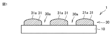
- FIG. 1 is a cross-sectional view schematically showing a lens element of a first embodiment.
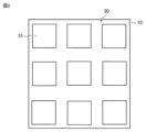
- FIG. 3 is a diagram showing a plan view of the lens element of the first embodiment.
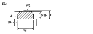
- FIG. 2 is a cross-sectional view schematically showing a microlens of the first embodiment.
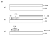
- FIG. 7 is a cross-sectional view schematically showing a lens element of a second embodiment. It is a partial sectional view showing each manufacturing process of the lens element of a 2nd embodiment.
- FIG. 3 is a schematic diagram showing how light travels in a mode in which a lens element is arranged and used in a solid-state image sensor.
- FIG. 2 is a schematic diagram showing how light travels in an embodiment in which the lens composition is arranged and used in a display device.
- the lens element of the present invention includes a substrate and a lens section, the lens section includes a plurality of microlenses arranged on the substrate and spaced apart from each other, and the plurality of microlenses have spectral characteristics.
- the microlens is made of a photocurable resin composition and has a convex curved surface on a surface not in contact with the substrate.
- FIG. 1 is a cross-sectional view schematically showing a lens element 1 of the first embodiment.
- the lens element 1 includes a substrate 10 and a lens section 30.
- the lens section 30 includes a plurality of microlenses 31 arranged on the substrate 10 and spaced apart from each other.
- the plurality of microlenses 31 include microlenses of two or more colors having different spectral characteristics.
- the microlens 31 is made of a photocurable resin composition and has a convex curved surface 31a on the surface not in contact with the substrate 10.
- the lens element 1 Since the lens element 1 includes microlenses 31 of two or more colors, it has a color separation function that is a function of a color filter. Furthermore, since the lens element 1 includes a plurality of microlenses 31 having a convex curved surface 31a, it has a light-condensing function of condensing light incident from the curved surface 31a. Furthermore, since the lens element 1 has a configuration in which the plurality of microlenses 31 are arranged apart from each other, it has a function of suppressing color mixture. More specifically, in the lens section 30, since the plurality of microlenses 31 are arranged apart from each other, gaps (spaces between the microlenses) 30a exist between the microlenses 31.
- Color mixing may occur when light that has passed through one microlens 31 enters another microlens 31, but in the lens section 30 of the present invention, light that has passed through one microlens 31 enters another microlens 31. It is necessary for the light to pass through the gap 30a between the microlenses 31 before entering the light beam. That is, in order to transmit through two boundaries (the boundary between the first microlens 31 and the gap 30a, and the boundary between the gap 30a and the second microlens 31), the microlenses 31 are arranged in contact with each other. Unlike the configuration described in 1, since the light always passes through the gap 30a, it is possible to suppress the frequency with which the light that has passed through the first microlens 31 enters the other microlenses 31.
- the lens element 1 has a function of suppressing color mixture.
- the lens element 1 since the lens element 1 is configured to have multiple functions at the same time, it is possible to achieve a thin film while realizing multiple functions. Further, the configuration can be simplified while realizing multiple functions.
- the plurality of microlenses 31 include microlenses of two or more colors with different spectral characteristics.
- a configuration including three colors of green (G), blue (B), and red (R), and a configuration including three colors of cyan (C), magenta (M), and yellow (Y) are used.
- FIG. 2 is a plan view of the lens section 30.
- the shape of the microlens 31 in plan view can be adjusted by the shape of the photomask used in the exposure step in the method for manufacturing the lens portion 30, and may be, for example, square, rectangular (for example, FIG. 2), circular, or elliptical. It may be.
- FIG. 3 shows a cross-sectional view of one microlens 31 in the lens section 30.
- the lens width W1 in contact with the substrate 10 is preferably 200 ⁇ m or less, more preferably 100 ⁇ m or less, further preferably 1 ⁇ m or more, and more preferably 2 ⁇ m or more.
- the lens width W1 may be the same or different in all cross sections.
- the lens width W1 has different values depending on the cross section. It is preferable that there is at least one cross section that satisfies the numerical range of the above-mentioned suitable lens width W1, and it is more preferable that it is satisfied for any cross section.
- the length of the gap 30a (FIG. 1) between the microlenses 31 in the lens portion 30 can be appropriately designed depending on the use of the lens element 1, but from the viewpoint of suppressing color mixture, it is important to
- the cross-sectional length (width) of the gap 30a with respect to the cross-sectional length (width) of the lens 31 is preferably 0.1 times or more and 1 time or less, more preferably 0.2 times or more and 0.8 times or less. preferable.
- the cross-sectional length (width) of the gap 30a is preferably 0.5 ⁇ m or more, more preferably 1.0 ⁇ m or more.
- the cross-sectional length (width) of the gap 30a is, for example, 200 ⁇ m or less.
- the cross-sectional length (width) of the gap 30a may be the same or different in all cross-sections, and may not be the same in all cross-sections.
- the cross-sectional length (width) may be different depending on the arrangement direction of the microlenses 31.
- FIG. 2 there is an example in which the cross-sectional length (width) of the gap 30a in the vertical arrangement of the microlenses 31 is longer than the cross-sectional length (width) of the gap 30a in the horizontal arrangement of the microlenses 31. It is shown.
- the ratio (W2/W1) of the lens width W2 at a height H of 90% of the lens height from the substrate surface to the lens width W1 in contact with the substrate 10 is preferably 0.7 or less, It is more preferably 0.6 or less, more preferably 0.4 or more, and even more preferably 0.5 or more.
- the lens element 1 of this embodiment can be used for the same purpose as a conventional lens element having multiple microlenses.
- it can be used by being placed in a solid-state image sensor.
- a solid-state image sensor it can be used by stacking it on a photoelectric conversion element layer consisting of a plurality of photoelectric conversion elements, and furthermore, a microlens is arranged to correspond to each photoelectric conversion element, and photoelectric conversion is performed through the microlens.
- a photoelectric conversion element layer consisting of a plurality of photoelectric conversion elements
- a microlens is arranged to correspond to each photoelectric conversion element, and photoelectric conversion is performed through the microlens.
- the specific form of the solid-state image sensor is not particularly limited, but for example, a plurality of photos forming the light receiving area of the solid-state image sensor (such as a CCD image sensor, a CMOS image sensor, or an organic CMOS image sensor) are arranged on a substrate. It is possible to configure a plurality of photoelectric conversion elements made of diodes, polysilicon, etc., and arrange microlenses so as to correspond to each photoelectric conversion element.
- the lens element 1 of this embodiment can be used by being placed in a display device, for example.
- a display device it can be used by stacking on a display element layer consisting of a plurality of display elements, and furthermore, microlenses are arranged to correspond to each display element, and light from the display elements is transmitted through the microlenses. By configuring the light to be emitted, it is possible to generate a color image and simultaneously improve light utilization efficiency.
- the specific form of the display device is not particularly limited, but can be used, for example, as a liquid crystal display device, an organic EL display device, etc. Also, micro LEDs, micro OLEDs, etc., which can enlarge and display images by projection, etc. It can be used for.
- FIG. 4 is a cross-sectional view schematically showing the lens element 2 of the second embodiment.
- the lens element 2 has a structure that further includes a coating layer 40 in addition to the structure of the lens element 1 of the first embodiment.
- the configuration other than the coating layer 40 is the same as the configuration of the lens element 1 of the first embodiment, so a description thereof will be omitted.
- the coating layer 40 has a structure that covers at least a part of the curved surface 31a of the plurality of microlenses 31, and has the effect of protecting the plurality of microlenses 31 and the lens section 30 by having such a structure.
- the covering layer 40 is preferably a continuous layer that connects the plurality of microlenses 31 to each other, and this structure has the effect of suppressing the separation of each microlens 31 from the substrate 10.
- the coating layer 40 preferably fills the gaps 30a between the microlenses 31 arranged on the substrate 10 at a distance from each other, and more preferably a plurality of coating layers This structure covers all surfaces of the microlens 31 that are not in contact with the substrate 10. With such a configuration, the contact area between the microlens 31 and the coating layer 40 can be increased, making it easier to suppress peeling between the layers.
- the refractive index of the coating layer 40 is preferably lower than the microlens 31 (than any of the plurality of microlenses 31) and higher than air. By adjusting the refractive index in this way, the light incident on the microlens 31 is easily totally reflected at the interface between the microlens 31 and the coating layer 40, and the efficiency of light utilization can be improved.
- the refractive index of the coating layer 40 is preferably 1.10 or more, more preferably 1.20 or more.
- the refractive index of the coating layer 40 is preferably 1.60 or less, more preferably 1.49 or less, even more preferably 1.45 or less.
- the refractive index of the coating layer means the refractive index at a wavelength of 589 nm.
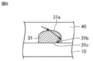
- FIG. 6 is a diagram schematically showing that leakage of light to the coating layer 40 can be suppressed in an embodiment in which the lens element 1 is arranged and used in a solid-state image sensor.
- the lens element 1 is arranged and used in a solid-state image sensor, light enters from the curved surface 31a of the macro lens 31. Even if the light reaches the side surface 31b within the microlens 31, the light is totally reflected at the interface between the microlens 31 and the coating layer 40, thereby suppressing leakage of the light to the coating layer 40. be able to.
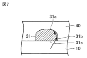
- FIG. 7 is a diagram schematically showing that leakage of light to the coating layer 40 can be suppressed in an embodiment in which the lens element 1 is arranged and used in a display device.
- the lens element 1 In a mode in which the lens element 1 is placed and used in a display device, light enters the microlens from the lower surface 31c facing the curved surface 31a. Even if the light reaches the side surface 31b within the microlens 31, the light is totally reflected at the interface between the microlens 31 and the coating layer 40, thereby suppressing leakage of the light to the coating layer 40. be able to.
- the surface 40a of the coating layer 40 on the side opposite to the substrate 10 is flat (the difference in height is small).
- the degree of flatness for example, if L is the distance from the surface of the substrate 10 to the surface 40a of the coating layer 40, the minimum value of L is preferably 1/2 or more of the maximum value of L, and 2/ More preferably, it is 3 or more. In this specification, it is assumed that the surface 40a of the coating layer 40 is flat when the minimum value of L is 1/2 or more of the maximum value of L.
- the coating layer 40 preferably has a surface roughness of 20 nm or less on the surface 40a opposite to the substrate 10, more preferably 10 nm or less.
- FIG. 4 shows a lens element 2 in which the lens portion 30 has three color microlenses 31 (referred to as "microlens 31A”, “microlens 31B”, and “microlens 31C", respectively).
- a manufacturing method for forming microlenses 31A, microlenses 31B, and microlenses 31C in this order in the lens portion 30 will be specifically described.
- the microlens 31A, the microlens 31B, and the microlens 31C each have different spectral characteristics and are formed from different photocurable resin compositions A, photocurable resin composition B, and photocurable resin composition C. shall be taken as a thing.
- the photocurable resin compositions A, B, and C may be resin compositions that differ only in the type of colorant contained and otherwise have the same composition; the colorant, resin, polymerizable compound, and light All types of polymerization initiators may be different.
- the refractive index of the microlenses 31A, 31B, and 31C formed from the photocurable resin compositions A, B, and C is preferably 1.50 or more, and more preferably 1.60 or more.
- the refractive index of the microlenses 31A, 31B, and 31C is preferably 1.80 or less.
- the microlenses 31A, 31B, and 31C may have the same or different refractive indexes.
- the refractive index of the microlens may mean the refractive index at a wavelength at which the transmittance is maximum in the visible light region of 380 nm to 780 nm, and may be compared with the refractive index of the coating layer 40. It may also mean the refractive index at a wavelength of 589 nm.
- the lens element 2 includes, in order, a step (a) of arranging a plurality of microlenses 31A, 31B, and 31C on a substrate 10 to form a lens portion 30, and a step (b) of forming a coating layer 40. .
- the lens element 1 of the first embodiment has at least the step (a) of arranging a plurality of microlenses 31A, 31B, and 31C on the substrate 10 to form the lens portion 30.
- a photocurable resin composition A is applied onto the substrate 10 to form a photocurable resin composition layer 20A (photocurable resin composition layer forming step, Step (a1)).
- the photocurable resin composition layer 20A is dried as necessary.
- the photocurable resin composition layer 20A is selectively exposed (exposure step, step (a2)).
- the selectively exposed region in the photocurable resin composition layer 20A is shown as a region 21A. Selective exposure of the photocurable resin composition layer 20A can be performed, for example, by irradiating light through the photomask 50 or by irradiating light in spots.
- the photocurable resin composition layer 20A is exposed with an exposure amount that is 2.0 times or more the saturation exposure amount. Thereafter, the photocurable resin composition layer 21A is developed (development step). A post-bake step may be provided after the development step, and the post-bake step may be performed following the development step. Through the above steps, the microlens 31A is formed on the substrate 10, as shown in FIG. 5(c).
- microlenses 31B are formed on the substrate 10.
- the microlenses 31B are formed by forming a photocurable resin composition layer on the substrate 10 on which the microlenses 31A are formed, using the photocurable resin composition B, by the same method as for forming the microlenses 31A described above. , an exposure step, and a development step in this order.
- a microlens 31C is formed on the substrate 10.
- the microlens 31C is formed by applying a photocurable resin composition C onto the substrate 10 on which the microlenses 31A and 31B are formed, using the same method as for forming the microlens 31A described above. It is formed by sequentially performing a material layer forming step, an exposure step, and a development step. Each step of forming the microlens 31A will be described in more detail below. The same applies to the details of each forming process of the microlenses 31B and 31C.
- the photocurable resin composition is not limited as long as it has the property of being polymerized by light irradiation in the exposure step and that the unexposed portion is eluted by development in the development step. Concerning the photocurable resin composition, specific examples will be shown later.
- the substrate 10 may be a glass plate such as quartz glass, borosilicate glass, alumina silicate glass, or soda lime glass whose surface is coated with silica, a resin plate such as polycarbonate, polymethyl methacrylate, or polyethylene terephthalate, silicon, or the above substrate.
- a material on which a thin film of aluminum, silver, silver/copper/palladium alloy, etc. is formed is used.
- Examples of methods for applying the photocurable resin composition include extrusion coating method, direct gravure coating method, reverse gravure coating method, CAP coating method, die coating method, etc. Further, coating may be performed using a coater such as a dip coater, a bar coater, a spin coater, a slit and spin coater, a slit coater (sometimes referred to as a die coater, a curtain flow coater, or a spinless coater), or a roller. Among these, it is preferable to apply using a spin coater.
- Examples of methods for drying the photocurable resin composition layer 20A include natural drying, ventilation drying, and vacuum drying.
- Specific heating temperatures include about 30 to 120°C, preferably about 60 to 100°C.
- the heating time is suitably about 10 seconds to 60 minutes, preferably about 30 seconds to 30 minutes.
- the vacuum drying is performed under a pressure of about 50 to 150 Pa and at a temperature of about 20 to 25°C.
- the solvent can be removed by the above-mentioned drying.
- the thickness of the photocurable resin composition layer 20A is not particularly limited, and can be adjusted as appropriate depending on the material used, the purpose of the lens element, etc.
- the thickness after drying is about 0.1 to 30 ⁇ m, preferably 0.
- the thickness is about .1 to 20 ⁇ m, more preferably about 0.3 to 10 ⁇ m, and still more preferably about 0.5 to 10 ⁇ m.
- Selective exposure of the photocurable resin composition layer 20A can be performed by exposing through a photomask 50, for example.
- a photomask 50 a mask is used in which a light-shielding portion is formed corresponding to a portion to be removed according to a desired pattern.
- the light source used for exposure may be a light source with a wavelength exceeding 300 nm or a light source with a wavelength of 300 nm or less. For example, light of less than 350 nm can be cut using a filter that cuts this wavelength range, or light around 436 nm, 408 nm, and 365 nm can be selectively extracted using a band pass filter that extracts these wavelength ranges.
- the light source include a mercury lamp, a light emitting diode, a metal halide lamp, a halogen lamp, and an excimer laser such as a KrF excimer laser and an ArF excimer laser.
- An exposure device such as a mask aligner or a stepper can be used to uniformly irradiate the entire exposed surface with parallel light and to accurately align the photomask 50 and the photocurable resin composition layer 20A. is preferred.
- the photocurable resin composition layer 20A is exposed with an exposure amount that is 2.0 times or more the saturation exposure amount.
- the photocurable resin composition layer 20A has a different residual film rate in the development step depending on the exposure amount in the exposure step.
- the residual film rate increases as the exposure dose increases, and after the residual film rate reaches 100%, the residual film rate remains at 100% even if the exposure dose increases. becomes.
- the saturation exposure amount of the photocurable resin composition layer 20A is the minimum exposure amount (hereinafter also referred to as “absolute minimum exposure amount") at which the residual film rate is 95% or more and 100% or less.
- the exposure amount is increased stepwise to measure the minimum measurement exposure amount (hereinafter also referred to as “measured minimum exposure amount”). Specifically, when the exposure amount is increased stepwise and the remaining film rate exceeds 95% for the first time when exposed at the exposure amount a and then exposed at the next larger exposure amount b, the remaining film rate is determined.
- the measured minimum exposure amount for which the value is 95% or more and 100% or less is measured as b, and therefore it can be seen that the absolute minimum exposure amount x is a value that satisfies a ⁇ x ⁇ b.
- the exposure amount in the exposure step is at least twice b, it is possible to make it at least twice the saturation exposure amount x. That is, if the measured minimum exposure amount b has been obtained, it is not necessarily necessary to determine the absolute minimum exposure amount x that corresponds to the saturated exposure amount.
- the measurement minimum exposure amount b can be measured, for example, by the following method.
- the layer was exposed using an exposure machine (TME-150RSK; manufactured by Topcon Co., Ltd., light source: ultra-high pressure mercury lamp) at an exposure dose (365 nm standard) in the range of 1 mJ/cm 2 to 500 mJ/cm 2 in an atmospheric atmosphere.
- the light is irradiated at 11 levels (1, 10, 15, 20, 40, 60, 100, 150, 200, 300, 500).
- this light irradiation is performed by passing the emitted light from an ultra-high pressure mercury lamp through an optical filter (UV-31; manufactured by Asahi Techno Glass Co., Ltd.).
- the thickness of the photocurable resin composition layer after light irradiation is measured and taken as the film thickness before development.
- a cured film is obtained by developing with the same developer and the same development conditions as in the development step, and performing post-baking. The thickness of this cured film is measured and used as the film thickness after development.
- the film thickness before development and the film thickness after development are measured using a contact film thickness measuring device (DEKT AK6M, manufactured by ULVAC Co., Ltd.).
- the residual film rate in the actual measurement is The minimum measured exposure amount b at which the film ratio is 95% or more and 100% or less is 100 mJ/cm 2 .
- the photocurable resin composition layer 20A should be exposed in the exposure step with an exposure amount of 200 mJ/cm 2 or more, which is more than twice the measured minimum exposure amount b. Therefore, exposure can be performed with an exposure amount that is twice or more than the saturation exposure amount.
- the shape of the surface of each dot can be adjusted with respect to the dot pattern obtained through the development step,
- the exposure amount is 2.0 times or more the saturation exposure amount, dots having a convex surface that can function as a lens can be obtained.
- the exposure amount of the photocurable resin composition layer 20A is not particularly limited as long as it is 2.0 times or more the saturated exposure amount, but it is 2.1 times or more, 2.2 times the saturated exposure amount. As mentioned above, the amount may be 2.3 times or more, and preferably 3.0 times or less the saturation exposure amount.
- a development step is performed to develop the photocurable resin composition layer 20A.
- the unexposed portion of the photocurable resin composition layer 20A is dissolved in the developer and removed, and is deposited on the substrate 10.
- a photocurable resin composition layer 20A having a pattern is formed.
- the developer an aqueous solution of an alkaline compound such as potassium hydroxide, sodium bicarbonate, sodium carbonate, or tetramethylammonium hydroxide is preferred.
- the concentration of these alkaline compounds in the aqueous solution is preferably 0.01 to 10% by mass, more preferably 0.03 to 5% by mass.
- the developer may contain a surfactant.
- the developing method may be any of the paddle method, dipping method, spray method, etc.
- the substrate 10 may be tilted at an arbitrary angle during development. After development, it is preferable to wash with water.
- a curing process may be performed by a post-exposure process using, for example, light with a wavelength of 254 to 350 nm, or a curing process may be performed by a post-baking process.
- the photocurable resin composition layer 20A is washed with water and then subjected to a post-baking process.
- the post-bake step is preferably performed after washing with water after the development step, since the time required for production can be shortened.
- the post-bake step is a step of heating the photocurable resin composition layer 20A on the substrate. Heating is usually performed using a heating device such as an oven or a hot plate.
- the heating temperature is preferably 60 to 260°C. When the heating temperature is set to such a temperature, unnecessary solvent can be prevented from remaining in the film.
- the heating time is preferably 1 to 120 minutes, more preferably 10 to 60 minutes.
- the photocurable resin composition used in the method for producing a lens of the present invention has the property of being polymerized by light irradiation in the exposure step, and that unexposed areas are eluted by development in the development step. It is not limited as long as it has desired spectral characteristics.
- the photocurable resin composition suitably used in the present invention will be explained.
- the compounds exemplified as each component can be used alone or in combination, unless otherwise specified.
- the photocurable resin composition of the present embodiment includes a resin (hereinafter referred to as resin (A)), a polymerizable compound (hereinafter referred to as polymerizable compound (C)), a photopolymerization initiator (hereinafter referred to as photopolymerization (hereinafter referred to as a polymerization initiator (D)), a colorant, and a solvent (hereinafter referred to as a solvent (E)). Furthermore, it may contain a polymerization initiation aid (hereinafter referred to as a polymerization initiation aid (H)).
- the resin (A) is preferably an alkali-soluble resin, and the structural unit (Aa) derived from at least one selected from the group consisting of unsaturated carboxylic acids and unsaturated carboxylic acid anhydrides (hereinafter referred to as "constituent units (Aa)”) ) is more preferable. It is more preferable that the resin (A) further includes a structural unit (Ab) having a carbazole ring (hereinafter referred to as “structural unit (Ab)").
- structural unit (Ab) represents at least one type of compound selected from the group consisting of acrylic acid and methacrylic acid. Notations such as “(meth)acryloyl” and “(meth)acrylate” have similar meanings.
- the monomer leading to the structural unit (Aa) includes, for example, Unsaturated monocarboxylic acids such as acrylic acid, methacrylic acid, crotonic acid, o-, m-, p-vinylbenzoic acid; Maleic acid, fumaric acid, citraconic acid, mesaconic acid, itaconic acid, 3-vinylphthalic acid, 4-vinylphthalic acid, 3,4,5,6-tetrahydrophthalic acid, 1,2,3,6-tetrahydrophthalic acid, dimethyl Unsaturated dicarboxylic acids such as tetrahydrophthalic acid and 1,4-cyclohexenedicarboxylic acid; Unsaturated dicarboxylic acid anhydrides such as maleic anhydride, citraconic anhydride, itaconic anhydride, vinyl phthalic anhydride, and tetrahydrophthalic anhydride; Examples include unsaturated acrylates containing a hydroxy group and a carboxy group in
- the monomer leading to the structural unit (Ab) include unsaturated compounds having a carbazole ring.
- the resin (A) contains the structural unit (Ab)
- the refractive index of the obtained film can be improved.
- the unsaturated compound having a carbazole ring is preferably a compound represented by formula (III).
- R 1 represents a hydrogen atom, a methyl group, or a hydroxymethyl group.
- R 2 to R 9 each independently represent a hydrogen atom, a halogen atom, a saturated hydrocarbon group having 1 to 20 carbon atoms, or an aryl group having 6 to 20 carbon atoms, and the hydrogen atoms contained in the saturated hydrocarbon group are , an alkoxy group or an aryl group.
- X is a single bond, an alkanediyl group having 1 or more carbon atoms, or -CO(-O-X 0 )m-(X 0 represents an alkanediyl group having 1 or more carbon atoms, and m represents an integer of 0 or more ).
- Examples of the compound represented by formula (III) include N-vinylcarbazole, N-allylcarbazole, N-(meth)acryloylcarbazole, 2-(9-carbazolyl)ethyl(meth)acrylate, 2-(9-carbazolyl) Examples include ethoxyethyl (meth)acrylate, 2-(9-carbazolyl)-2-methylethyl (meth)acrylate, and 2-(9-carbazolyl)-1-methylethyl (meth)acrylate.
- the resin (A) may have a structural unit (Ac) different from the structural unit (Aa) and the structural unit (Ab).
- the structural unit (Ac) is a structural unit derived from an unsaturated compound having a cyclic ether structure having 2 to 4 carbon atoms (for example, at least one selected from the group consisting of an oxirane ring, an oxetane ring, and a tetrahydrofuran ring); Examples include structural units having an ethylenically unsaturated bond in the chain and other structural units.
- Examples of the unsaturated compound having a cyclic ether structure having 2 to 4 carbon atoms include glycidyl (meth)acrylate, ⁇ -methylglycidyl (meth)acrylate, glycidyl vinyl ether, glycidyloxymethylstyrene; vinylcyclohexene monooxide, 1,2-epoxy-4-vinylcyclohexane (e.g.
- Celoxide 2000 manufactured by Daicel Corporation
- 3,4-epoxycyclohexylmethyl (meth) ) acrylate for example, Cyclomer A400; manufactured by Daicel Corporation
- 3,4-epoxycyclohexylmethyl (meth)acrylate for example, Cyclomer M100; manufactured by Daicel Corporation
- 3,4-epoxytricyclo[5 .2.1.0 2,6 ] Decyl (meth)acrylate; 3-methyl-3-(meth)acryloyloxymethyloxetane, 3-ethyl-3-(meth)acryloyloxymethyloxetane; Tetrahydrofurfuryl (meth) ) acrylate, etc.
- the structural unit having a structural unit having an ethylenically unsaturated bond in the side chain can be obtained by adding an unsaturated compound having a cyclic ether structure having 2 to 4 carbon atoms to a copolymer containing the structural unit (Aa), or adding an unsaturated compound having a cyclic ether structure having 2 to 4 carbon atoms. It can be produced by adding an unsaturated carboxylic acid to a copolymer containing a structural unit derived from an unsaturated compound having 2 to 4 cyclic ether structures. The latter resin may be further reacted with a carboxylic acid anhydride.
- Examples of monomers leading to other structural units include: Methyl (meth)acrylate, butyl (meth)acrylate cyclohexyl (meth)acrylate, 2-methylcyclohexyl (meth)acrylate, tricyclo[5.2.1.0 2,6 ]decane-8-yl (meth)acrylate, tricyclo [5.2.1.0 2,6 ]Decen-8-yl (meth)acrylate, benzyl (meth)acrylate, 2-hydroxyethyl (meth)acrylate N-phenylmaleimide, N-cyclohexylmaleimide, N-benzylmaleimide , styrene, vinyltoluene and the like.
- the weight average molecular weight (Mw) of the resin (A) in terms of polystyrene is preferably 3,000 to 100,000, more preferably 5,000 to 50,000, even more preferably 5,000 to 20,000, particularly preferably is between 5,000 and 10,000.
- Mw weight average molecular weight
- the dispersity [weight average molecular weight (Mw)/number average molecular weight (Mn)] of the resin (A) is preferably 1.1 to 6.0, more preferably 1.2 to 4.0. When the degree of dispersion is within the above range, the resulting film tends to have excellent chemical resistance.
- the acid value of the resin (A) is preferably 30 mg-KOH/g or more and 180 mg-KOH/g or less, more preferably 40 mg-KOH/g or more and 150 mg-KOH/g or less, and even more preferably 50 mg-KOH/g or more and 135 mg or less. -KOH/g or less.
- the acid value is a value measured as the amount (mg) of potassium hydroxide required to neutralize 1 g of resin, and can be determined by titration using an aqueous potassium hydroxide solution. When the acid value of the resin (A) is within the above range, the resulting film tends to have excellent adhesion to the substrate.
- the content of the resin (A) in the photocurable resin composition of the present invention is preferably 5% by mass or more and 70% by mass or less, more preferably 5% by mass or more and 70% by mass or less, based on the total solid content of the photocurable resin composition of the present invention. is 10% by mass or more and 60% by mass or less, more preferably 15% by mass or more and 55% by mass or less.
- the content of the resin (A) is within the above range, the resulting film tends to have excellent heat resistance, as well as excellent adhesion to the substrate and chemical resistance.
- the solid content of the photocurable resin composition refers to the amount obtained by subtracting the content of the solvent (E) from the total amount of the photocurable resin composition of the present invention.
- the polymerizable compound (C) is a monomer that reacts with heat or the action of a photopolymerization initiator (D), and examples of the monomer include compounds having an ethylenically unsaturated bond, preferably (meth)acrylic. Examples include acid ester compounds.
- the polymerizable compound is preferably a (meth)acrylic compound having three or more (meth)acryloyl groups, such as trimethylolpropane tri(meth)acrylate, pentaerythritol tri(meth)acrylate, pentaerythritol tetra(meth)acrylate, More preferred are dipentaerythritol penta(meth)acrylate and dipentaerythritol hexa(meth)acrylate.
- the weight average molecular weight of the polymerizable compound (C) is preferably 150 or more and 2,900 or less, more preferably 250 or more and 1,500 or less.
- the content of the polymerizable compound (C) in the photocurable resin composition of the present invention may be, for example, 1% by mass or more and 99% by mass or less, based on the total solid content of the photocurable resin composition.
- the content is preferably 5% by mass or more and 90% by mass or less, more preferably 8% by mass or more and 80% by mass or less, and still more preferably 10% by mass or more and 70% by mass or less.
- the resulting film can have good chemical resistance and mechanical strength.
- the photopolymerization initiator (D) is not particularly limited as long as it is a compound that generates active radicals, acids, etc. by the action of light and can initiate polymerization of the polymerizable compound (C), and may be any known photopolymerization initiator. Agents can be used.
- the photopolymerization initiator (D) is preferably a photopolymerization initiator containing at least one selected from the group consisting of O-acyloxime compounds, alkylphenone compounds, triazine compounds, acylphosphine oxide compounds, and biimidazole compounds; - A photopolymerization initiator containing an acyloxime compound is more preferred.
- photopolymerization initiators tend to have high sensitivity and high transmittance in the visible light region.
- photopolymerization initiators include N-benzoyloxy-1-(4-phenylsulfanylphenyl)butan-1-one-2-imine, N-benzoyloxy-1-(4-phenylsulfanylphenyl) Octan-1-one-2-imine, N-benzoyloxy-1-(4-phenylsulfanylphenyl)-3-cyclopentylpropan-1-one-2-imine, 2-methyl-2-morpholino-1-(4 -methylsulfanylphenyl)propan-1-one, 2-dimethylamino-1-(4-morpholinophenyl)-2-benzylbutan-1-one, 1-hydroxycyclohexylphenylketone, 2,4-bis(trichloromethyl) -6-Piperonyl-1,3,5-triazine, 2,4,6-trimethylbenz
- the content of the photopolymerization initiator (D) in the photocurable resin composition of the present invention is preferably 0.1 mass parts with respect to 100 parts by mass of the total amount of the resin (A) and the polymerizable compound (C). parts or more and 30 parts by mass or less, more preferably 0.3 parts by mass or more and 20 parts by mass or less.
- the transmittance of the visible light transmitting portion of the resulting pattern tends to be high.
- the polymerization initiation aid (H) is a compound used together with the photopolymerization initiator (D) to promote the polymerization of the polymerizable compound (C) whose polymerization has been initiated by the photopolymerization initiator (D), or a polymerization promoter. It is a sensitizing agent. When a polymerization initiation aid (H) is included, it is usually used in combination with a photopolymerization initiator (D).
- polymerization initiation aid examples include 4,4'-bis(dimethylamino)benzophenone (commonly known as Michler's ketone), 4,4'-bis(diethylamino)benzophenone, 9,10-dimethoxyanthracene, and 2,4-diethylthioxanthone. , N-phenylglycine, and the like.
- the content is preferably based on 100 parts by mass of the total content of the resin (A) and the polymerizable compound (C). is 0.1 parts by mass or more and 30 parts by mass or less, more preferably 0.2 parts by mass or more and 10 parts by mass or less.
- the amount of the polymerization initiation aid (H) is within the above range, the sensitivity tends to be even higher when forming a pattern.
- the colorant includes at least one selected from the group consisting of dyes and pigments.
- the colorant preferably comprises a combination of two dyes or a combination of at least one dye and at least one pigment, more preferably a combination of two dyes or one dye and one pigment. including combinations of
- Known dyes can be used as the dyes, including solvent dyes, acid dyes, direct dyes, mordant dyes, etc.
- solvent, acid, basic examples include compounds classified as dyes such as reactive, direct, disperse, mordant, or bat, and known dyes described in Dyeing Notes (Shirosensha).
- the dye may be appropriately selected depending on the desired spectral characteristics of the microlens array. These dyes may be used alone or in combination of two or more.
- the dye is preferably an organic solvent soluble dye.
- pigments include organic pigments and inorganic pigments, including compounds classified as pigments in the Color Index (published by The Society of Dyers and Colourists).
- the photocurable resin composition of the present invention contains a solvent (E).
- the solvent (E) is not particularly limited, and includes solvents commonly used in the field. For example, ester solvents (solvents that contain -COO- but no -O- in the molecule), ether solvents (solvents that contain -O- but no -COO- in the molecule), and ether ester solvents (solvents that contain -O- but no -COO- in the molecule).
- solvents containing -COO- and -O- solvents containing -COO- and -O-
- ketone solvents solvents containing -CO- in the molecule but not -COO-
- alcohol solvents solvents containing OH in the molecule, -O-, - (CO- and -COO--free solvents), aromatic hydrocarbon solvents, amide solvents, dimethyl sulfoxide, and the like.
- Solvents include methyl lactate, ethyl lactate, butyl lactate, methyl 2-hydroxyisobutanoate, ethyl acetate, n-butyl acetate, isobutyl acetate, pentyl formate, isopentyl acetate, butyl propionate, isopropyl butyrate, ethyl butyrate, butyl butyrate, Ester solvents of methyl pyruvate, ethyl pyruvate, propyl pyruvate, methyl acetoacetate, ethyl acetoacetate, cyclohexanol acetate and ⁇ -butyrolactone;
- Ether solvents such as ethylene glycol monobutyl ether, diethylene glycol monomethyl ether 3-methoxy-3-methylbutanol diethylene glycol dimethyl ether diethylene glycol ethyl methyl ether; ethyl 3-methoxypropionate, methyl 3-ethoxypropionate, 3-methoxybutyl acetate, propylene glycol monomethyl Ether ester solvents such as ether acetate, ethylene glycol monoethyl ether acetate, diethylene glycol monoethyl ether acetate; 4-hydroxy-4-methyl-2-pentanone heptanone, 4-methyl-2-pentanone, cyclopentanone, cyclohexanone, etc.
- alcohol solvents such as butanol and hexanol propylene glycol
- amide solvents such as N,N-dimethylformamide, N,N-dimethylacetamide and N-methylpyrrolidone.
- More preferred solvents include propylene glycol monomethyl ether acetate, propylene glycol monomethyl ether, ethyl lactate, ethyl 3-ethoxypropionate and 4-hydroxy-4-methyl-2-pentanone.
- propylene glycol monomethyl ether acetate propylene glycol monomethyl ether, ethyl 3-ethoxypropionate, ethyl lactate, ethylene glycol ethyl methyl ether, cyclohexanone, methoxybutanol and methoxybutyl acetate are preferred, and propylene glycol monomethyl ether acetate is more preferred. .
- the content of the solvent (E) in the photocurable resin composition of the present invention is usually 99.99% by mass or less, preferably 40% by mass or more and 99% by mass, based on the total amount of the photocurable resin composition.
- the content is more preferably 50% by mass or more and 97% by mass or less, still more preferably 60% by mass or more and 95% by mass or less, even more preferably 65% by mass or more and 90% by mass or less.
- the total solid content of the photocurable resin composition of the present invention is usually 0.01% by mass or more, preferably 1% by mass or more and 60% by mass or less, more preferably 3% by mass or more and 50% by mass.
- the content is more preferably 5% by mass or more and 40% by mass or less, even more preferably 10% by mass or more and 35% by mass or less.
- the photocurable resin composition of the present invention may optionally contain fillers, other polymer compounds, leveling agents, antioxidants, curing agents, ultraviolet absorbers, chain transfer agents, adhesion promoters, etc. It may also contain additives known in the art.
- the photocurable resin composition of this embodiment includes a resin (A), a polymerizable compound (C), a photoinitiator (D), a colorant, and a solvent (E), and further a polymerization initiation aid (H). It can be manufactured by mixing other components such as, etc. by a known method. After mixing, it is preferable to filter through a filter with a pore size of about 0.05 to 1.0 ⁇ m.
- the covering layer 40 is formed from a resin composition for forming a covering layer.
- the resin composition for forming the coating layer includes a resin, a polymerizable compound, a photopolymerization initiator, and the like.
- the refractive index of the resin composition for forming the coating layer should be lower than the refractive index of the photocurable resin composition, and may be the same as the resin, polymerizable compound, and photopolymerization initiator described in the photocurable resin composition described above. are used.
- the resin in the resin composition for forming a coating layer preferably has the above-mentioned structural unit (Aa) and structural unit (Ac).
- the coating layer forming resin composition As a method for laminating the coating layer forming resin composition on the substrate 10, the coating layer forming resin composition is applied to the surface of the lens portion 30 so as to cover all exposed surfaces of each microlens 31. Then, it can be cured by irradiating active energy rays.
- Coating can be performed by a conventional method such as a microgravure coating method, a roll coating method, a dipping coating method, a spin coating method, a die coating method, a cast transfer method, a flow coating method, and a spray coating method. From the viewpoint of easily improving the optical properties of the coating layer, it is preferable to laminate the coating layer-forming composition by a microgravure coating method or a die coating method.
- the composition for forming a coating layer is cured by irradiation with active energy rays, and the desired coating layer is obtained.
- active energy rays include electron beams, ultraviolet rays, and visible rays, and are appropriately selected depending on the type of coating layer forming composition used.
- the intensity of the active energy rays to be irradiated, the irradiation time, etc. are appropriately selected depending on the type of the coating layer forming composition used, the thickness of the coating layer, etc.
- the active energy rays may be irradiated in an inert gas atmosphere.
- the active energy rays may be irradiated, for example, in a container sealed with an inert gas, and nitrogen gas, argon gas, etc. can be used as the inert gas.
Landscapes
- Physics & Mathematics (AREA)
- General Physics & Mathematics (AREA)
- Optics & Photonics (AREA)
- Engineering & Computer Science (AREA)
- Manufacturing & Machinery (AREA)
- Chemical & Material Sciences (AREA)
- Crystallography & Structural Chemistry (AREA)
- Optical Filters (AREA)
- Lenses (AREA)
- Solid State Image Pick-Up Elements (AREA)
Abstract
Description
[1] 基板と、レンズ部とを有するレンズ素子であって、
前記レンズ部は、前記基板上に互いに離間して配置されている複数のマイクロレンズを備え、
前記複数のマイクロレンズは、分光特性が異なる2色以上のマイクロレンズを含み、
前記マイクロレンズは、光硬化性樹脂組成物からなり、前記基板に接しない表面に凸状の曲面を有する、レンズ素子。
[2] 被覆層をさらに有し、
前記被覆層は、前記複数のマイクロレンズの前記曲面の少なくとも一部を被覆する、[1]に記載のレンズ素子。
[3] 前記被覆層は、互いに離間して配置されている前記マイクロレンズの間の空間に充填されている、[2]に記載のレンズ素子。
[4] 前記被覆層は、前記複数のマイクロレンズの前記基板と接していない全ての表面を被覆し、かつ表面が平坦である、[3]に記載のレンズ素子。
[5] 前記被覆層は、屈折率が前記マイクロレンズの屈折率より低い、[2]~[4]のいずれか1項に記載のレンズ素子。
[6] 前記被覆層は、屈折率が1.1以上である、[2]~[5]のいずれか1項に記載のレンズ素子。
[7] 前記複数のマイクロレンズは、緑、青、および赤、またはシアン、マゼンタ、およびイエローのマイクロレンズを含む、[1]~[6]のいずれか1項に記載のレンズ素子。
[8] [2]~[7]のいずれか1項に記載のレンズ素子の製造方法であって、
前記基板の上に前記複数のマイクロレンズを配置して前記レンズ部を形成する工程(a)と、
被覆層形成用樹脂組成物を、前記レンズ部の表面に塗布して塗膜を形成する工程(b1)と、
前記塗膜を硬化する工程(b2)と、をこの順に有する製造方法。
[9] 前記工程(a)は、
前記基板の上に前記光硬化性樹脂組成物を塗布して光硬化性樹脂組成物層を形成する工程(a1)と、
前記光硬化性樹脂組成物層を選択的に露光する工程(a2)と、を有し、
前記工程(a2)において、前記光硬化性樹脂組成物層を飽和露光量の2.0倍以上の露光量で露光する、[8]に記載の製造方法。
[10] [8]または[9]に記載の製造方法で用いられる被覆層形成用樹脂組成物。
[11] [1]~[7]のいずれか1項に記載のレンズ素子を備える、固体撮像素子。
[12] [1]~[7]のいずれか1項に記載のレンズ素子を備える、表示装置。
<第1の実施形態>
図1は、第1の実施形態のレンズ素子1を模式的に示す断面図である。レンズ素子1は、基板10と、レンズ部30とを有する。レンズ部30は、基板10上に互いに離間して配置されている複数のマイクロレンズ31を備える。複数のマイクロレンズ31は、分光特性が異なる2色以上のマイクロレンズを含む。マイクロレンズ31は、光硬化性樹脂組成物からなり、基板10に接しない表面に凸状の曲面31aを有する。
図4は、第2の実施形態のレンズ素子2を模式的に示す断面図である。レンズ素子2は、第1の実施形態のレンズ素子1の構成に加えて被覆層40をさらに有する構成である。被覆層40以外の構成は、第1の実施形態のレンズ素子1の構成と同じであるので、説明を省略する。
第2の実施形態のレンズ素子2の製造方法の一例を説明する。図4はレンズ部30が3色のマイクロレンズ31(それぞれ、「マイクロレンズ31A」、「マイクロレンズ31B」、「マイクロレンズ31C」、とする。)を有するレンズ素子2である。レンズ部30において、マイクロレンズ31A、マイクロレンズ31B、マイクロレンズ31Cの順に形成する製造方法について具体的に説明する。マイクロレンズ31A、マイクロレンズ31B、マイクロレンズ31Cは、それぞれ異なる分光特性を有し、異なる光硬化性樹脂組成物A、光硬化性樹脂組成物B、光硬化性樹脂組成物Cから形成されているものとする。光硬化性樹脂組成物A、B、Cは、例えば、含まれる着色剤の種類のみが異なり、ほかは同じ組成の樹脂組成物を用いてもよく、着色剤、樹脂、重合性化合物、及び光重合開始剤の種類が全て異なっていてもよい。光硬化性樹脂組成物A、B、Cにより形成されるマイクロレンズ31A、31B、31Cの屈折率は、好ましくは1.50以上であり、より好ましくは1.60以上である。マイクロレンズ31A、31B、31Cの屈折率は、好ましくは1.80以下である。マイクロレンズ31A、31B、31Cは、屈折率が同じであっても異なっていてもよい。なお、本願発明においてマイクロレンズの屈折率は、380nm-780nmの可視光領域における透過率が最大となる波長における屈折率を意味してもよく、また被覆層40の屈折率との対比ができるように589nmの波長における屈折率を意味するものとしてもよい。
工程(a)は、基板10の上にマイクロレンズ31A、マイクロレンズ31B、マイクロレンズ31Cを順に形成する工程を有する。かかる工程について説明する。
光硬化性樹脂組成物としては、露光工程での光の照射により重合し、かつ未露光部は現像工程での現像により溶出する性質を有するものであれば限定されない。光硬化性樹脂組成物については、後段で具体例を示す。
光硬化性樹脂組成物層20Aの選択的な露光は、例えば、フォトマスク50を介して露光することにより行うことができる。フォトマスク50として、目的とするパターンに応じて除去したい部分に対応して遮光部が形成されたマスクを用いる。露光に用いられる光源としては、波長300nmを超える光源であってもよく、波長300nm以下の光源であってもよい。例えば、350nm未満の光を、この波長域をカットするフィルタを用いてカットしたり、436nm付近、408nm付近、365nm付近の光を、これらの波長域を取り出すバンドパスフィルタを用いて選択的に取り出したりしてもよい。また、248nm(KrF線)、193nm(ArF線)などを用いてもよい。光源としては、水銀灯、発光ダイオード、メタルハライドランプ、ハロゲンランプや、KrFエキシマレーザ、ArFエキシマレーザ等のエキシマレーザーが挙げられる。露光面全体に均一に平行光線を照射することや、フォトマスク50と光硬化性樹脂組成物層20Aとの正確な位置合わせを行うことができるため、マスクアライナ、ステッパ等の露光装置を用いることが好ましい。
残膜率(%)=(現像後の膜厚/現像前の膜厚)×100 (1)
光硬化性樹脂組成物層20Aと同一の組成の光硬化性樹脂組成物を同一の塗布方法によって基板上に塗布し同一の条件で乾燥して得られた同一の厚みの光硬化性樹脂組成物層に対して、露光機(TME-150RSK;トプコン(株)製、光源;超高圧水銀灯)を用いて、大気雰囲気下、露光量(365nm基準)を1mJ/cm2~500mJ/cm2の範囲で11水準(1,10,15,20,40,60,100,150,200,300,500)で順次増加させてそれぞれ光照射する。なお、この光照射は、超高圧水銀灯からの放射光を、光学フィルタ(UV-31;旭テクノグラス(株)製)を通過させて行う。光照射後の光硬化性樹脂組成物層の厚みを測定して現像前の膜厚とする。現像工程と同じ現像液及び同じ現像条件で現像し、ポストベークを行うことにより硬化膜を得る。かかる硬化膜の厚みを測定して現像後の膜厚とする。現像前の膜厚と現像後の膜厚は、接触式膜厚測定装置(DEKT AK6M、(株)アルバック製)により測定する。
露光工程後、光硬化性樹脂組成物層20Aを現像する現像工程を行う。露光後の光硬化性樹脂組成物層20Aを現像液に接触させて現像することにより、光硬化性樹脂組成物層20Aの未露光部が現像液に溶解して除去されて、基板10上にパターンを有する光硬化性樹脂組成物層20Aが形成される。現像液としては、水酸化カリウム、炭酸水素ナトリウム、炭酸ナトリウム、水酸化テトラメチルアンモニウム等のアルカリ性化合物の水溶液が好ましい。これらのアルカリ性化合物の水溶液中の濃度は、好ましくは0.01~10質量%、より好ましくは0.03~5質量%である。さらに、現像液は、界面活性剤を含んでいてもよい。現像方法は、パドル法、ディッピング法及びスプレー法等のいずれでもよい。さらに現像時に基板10を任意の角度に傾けてもよい。現像後は、水洗することが好ましい。
現像工程後に、例えば波長254~350nmの光を用いた後露光工程により硬化する工程を行ってもよく、ポストベーク工程により硬化する工程を行ってもよい。好ましくは、光硬化性樹脂組成物層20Aを水洗しポストベーク工程を行う。ポストベーク工程は、製造に要する時間を短くできる点で、現像工程後の水洗後に続いて行うことが好ましい。ポストベーク工程を行うことによりレンズの耐久性(耐溶剤性)を向上させることができる。
本発明のレンズを製造する方法において用いられる光硬化性樹脂組成物は、上述の通り、露光工程での光の照射により重合し、かつ未露光部は現像工程での現像により溶出する性質を有するものであり、また所望の分光特性を有するものであれば限定されない。以下、本発明において好適に用いられる光硬化性樹脂組成物の一形態を説明する。各成分として例示する化合物は、特に断りのない限り、単独で又は複数種を組合せて使用することができる。
樹脂(A)は、アルカリ可溶性樹脂であることが好ましく、不飽和カルボン酸及び不飽和カルボン酸無水物からなる群から選ばれる少なくとも1種に由来する構成単位(Aa)(以下「構成単位(Aa)」と称する。)を有する樹脂がより好ましい。樹脂(A)は、さらに、カルバゾール環を有する構成単位(Ab)(以下「構成単位(Ab)」と称する。)を有することがより好ましい。なお、本明細書において、「(メタ)アクリル酸」とは、アクリル酸及びメタクリル酸よりなる群から選ばれる少なくとも1種の化合物を表す。「(メタ)アクリロイル」及び「(メタ)アクリレート」等の表記も、同様の意味を有する。
アクリル酸、メタクリル酸、クロトン酸、o-、m-、p-ビニル安息香酸等の不飽和モノカルボン酸類;
マレイン酸、フマル酸、シトラコン酸、メサコン酸、イタコン酸、3-ビニルフタル酸、4-ビニルフタル酸、3,4,5,6-テトラヒドロフタル酸、1,2,3,6-テトラヒドロフタル酸、ジメチルテトラヒドロフタル酸、1,4-シクロヘキセンジカルボン酸等の不飽和ジカルボン酸類;
無水マレイン酸、シトラコン酸無水物、イタコン酸無水物、ビニルフタル酸無水物,テトラヒドロフタル酸無水物等の不飽和ジカルボン酸類無水物;
α-(ヒドロキシメチル)アクリル酸のような、同一分子中にヒドロキシ基及びカルボキシ基を含有する不飽和アクリレート類等が挙げられる。
これらのうち、共重合反応性の点や得られる樹脂のアルカリ水溶液への溶解性の点から、アクリル酸、メタクリル酸等が好ましい。

R2~R9は、互いに独立に、水素原子、ハロゲン原子、炭素数1~20の飽和炭化水素基又は炭素数6~20のアリール基を表し、該飽和炭化水素基に含まれる水素原子は、アルコキシ基又はアリール基で置換されていてもよい。
Xは、単結合、炭素数1以上のアルカンジイル基、もしくは-CO(-O-X0)m-(X0は炭素数1以上のアルカンジイル基を表し、mは0以上の整数を表す。)を表す。
メチル(メタ)アクリレート、ブチル(メタ)アクリレートシクロヘキシル(メタ)アクリレート、2-メチルシクロヘキシル(メタ)アクリレート、トリシクロ[5.2.1.02,6]デカン-8-イル(メタ)アクリレート、トリシクロ[5.2.1.02,6]デセン-8-イル(メタ)アクリレート、ベンジル(メタ)アクリレート、2-ヒドロキシエチル(メタ)アクリレートN-フェニルマレイミド、N-シクロヘキシルマレイミド、N-ベンジルマレイミド、スチレン、ビニルトルエン等が挙げられる。
重合性化合物(C)は、熱又は光重合開始剤(D)の作用により反応するモノマーであり、該モノマーとして、例えば、エチレン性不飽和結合を有する化合物が挙げられ、好ましくは(メタ)アクリル酸エステル化合物が挙げられる。
重合性化合物(C)の重量平均分子量は、好ましくは150以上2,900以下、より好ましくは250以上1,500以下である。
光重合開始剤(D)は、光の作用により活性ラジカル、酸等を発生し、重合性化合物(C)の重合を開始しうる化合物であれば特に限定されることなく、公知の光重合開始剤を用いることができる。光重合開始剤(D)としては、O-アシルオキシム化合物、アルキルフェノン化合物、トリアジン化合物、アシルホスフィンオキサイド化合物及びビイミダゾール化合物からなる群から選ばれる少なくとも1種を含む光重合開始剤が好ましく、O-アシルオキシム化合物を含む光重合開始剤がより好ましい。これらの光重合開始剤であると、高感度であり、かつ可視光領域における透過率が高くなる傾向がある。
このような光重合開始剤としては、例えば、N-ベンゾイルオキシ-1-(4-フェニルスルファニルフェニル)ブタン-1-オン-2-イミン、N-ベンゾイルオキシ-1-(4-フェニルスルファニルフェニル)オクタン-1-オン-2-イミン、N-ベンゾイルオキシ-1-(4-フェニルスルファニルフェニル)-3-シクロペンチルプロパン-1-オン-2-イミン、2-メチル-2-モルホリノ-1-(4-メチルスルファニルフェニル)プロパン-1-オン、2-ジメチルアミノ-1-(4-モルホリノフェニル)-2-ベンジルブタン-1-オン、1-ヒドロキシシクロヘキシルフェニルケトン、2,4-ビス(トリクロロメチル)-6-ピペロニル-1,3,5-トリアジン、2,4,6-トリメチルベンゾイルジフェニルホスフィンオキサイド、2,2’-ビス(2-クロロフェニル)-4,4’,5,5’-テトラフェニルビイミダゾール等が挙げられる。
重合開始助剤(H)は、光重合開始剤(D)とともに、光重合開始剤(D)によって重合が開始された重合性化合物(C)の重合を促進するために用いられる化合物、もしくは増感剤である。重合開始助剤(H)を含む場合、通常、光重合開始剤(D)と組み合わせて用いられる。
着色剤は、染料及び顔料からなる群から選択される少なくとも1種を含む。着色剤は、好ましくは2種の染料の組合せ又は少なくとも1種の染料と少なくとも1種の顔料との組合せを含み、より好ましくは2種の染料の組合せ又は1種の染料と1種の顔料との組合せを含む。
本発明の光硬化性樹脂組成物は、溶剤(E)を含有する。溶剤(E)としては、特に限定されず、当該分野で通常使用される溶剤を挙げることができる。例えば、エステル溶剤(分子内に-COO-を含み、-O-を含まない溶剤)、エーテル溶剤(分子内に-O-を含み、-COO-を含まない溶剤)、エーテルエステル溶剤(分子内に-COO-と-O-とを含む溶剤)、ケトン溶剤(分子内に-CO-を含み、-COO-を含まない溶剤)、アルコール溶剤(分子内にOHを含み、-O-、-CO-及び-COO-を含まない溶剤)、芳香族炭化水素溶剤、アミド溶剤、ジメチルスルホキシド等が挙げられる。
溶剤としては、プロピレングリコールモノメチルエーテルアセテート、プロピレングリコールモノメチルエーテル、乳酸エチル、3-エトキシプロピオン酸エチル及び4-ヒドロキシ-4-メチル-2-ペンタノンがより好ましい。
本発明の光硬化性樹脂組成物には、必要に応じて、充填剤、その他の高分子化合物、レベリング剤、酸化防止剤、硬化剤、紫外線吸収剤、連鎖移動剤、密着促進剤等、当該技術分野において公知の添加剤を含有していてもよい。
本実施形態の光硬化性樹脂組成物は、樹脂(A)、重合性化合物(C)、光重合開始剤(D)、着色剤、及び溶剤(E)、さらに、重合開始助剤(H)等のその他の成分を、公知の方法で混合することにより製造することができる。混合後は、孔径0.05~1.0μm程度のフィルタでろ過することが好ましい。
被覆層40は被覆層形成用樹脂組成物により形成される。被覆層形成用樹脂組成物としては、樹脂、重合性化合物、及び光重合開始剤等を含む。被覆層形成用樹脂組成物の屈折率は、光硬化性樹脂組成物の屈折率より低ければよく、前述の光硬化性樹脂組成物で記載した樹脂、重合性化合物、及び光重合開始剤と同様のものが使用される。被覆層形成用樹脂組成物における樹脂としては、前述の構成単位(Aa)及び構成単位(Ac)を有することが好ましい。
Claims (12)
- 基板と、レンズ部とを有するレンズ素子であって、
前記レンズ部は、前記基板上に互いに離間して配置されている複数のマイクロレンズを備え、
前記複数のマイクロレンズは、分光特性が異なる2色以上のマイクロレンズを含み、
前記マイクロレンズは、光硬化性樹脂組成物からなり、前記基板に接しない表面に凸状の曲面を有する、レンズ素子。 - 被覆層をさらに有し、
前記被覆層は、前記複数のマイクロレンズの前記曲面の少なくとも一部を被覆する、請求項1に記載のレンズ素子。 - 前記被覆層は、互いに離間して配置されている前記マイクロレンズの間の空間に充填されている、請求項2に記載のレンズ素子。
- 前記被覆層は、前記複数のマイクロレンズの前記基板と接していない全ての表面を被覆し、かつ表面が平坦である、請求項3に記載のレンズ素子。
- 前記被覆層は、屈折率が前記マイクロレンズの屈折率より低い、請求項4に記載のレンズ素子。
- 前記被覆層は、屈折率が1.1以上である、請求項5に記載のレンズ素子。
- 前記複数のマイクロレンズは、緑、青、および赤、またはシアン、マゼンタ、およびイエローのマイクロレンズを含む、請求項1又は2に記載のレンズ素子。
- 請求項2または3に記載のレンズ素子の製造方法であって、
前記基板の上に前記複数のマイクロレンズを配置して前記レンズ部を形成する工程(a)と、
被覆層形成用樹脂組成物を、前記レンズ部の表面に塗布して塗膜を形成する工程(b1)と、
前記塗膜を硬化する工程(b2)と、をこの順に有する製造方法。 - 前記工程(a)は、
前記基板の上に前記光硬化性樹脂組成物を塗布して光硬化性樹脂組成物層を形成する工程(a1)と、
前記光硬化性樹脂組成物層を選択的に露光する工程(a2)と、を有し、
前記工程(a2)において、前記光硬化性樹脂組成物層を飽和露光量の2.0倍以上の露光量で露光する、請求項8に記載の製造方法。 - 請求項8に記載の製造方法で用いられる被覆層形成用樹脂組成物。
- 請求項1または2に記載のレンズ素子を備える、固体撮像素子。
- 請求項1または2に記載のレンズ素子を備える、表示装置。
Priority Applications (2)
| Application Number | Priority Date | Filing Date | Title |
|---|---|---|---|
| KR1020247041053A KR20250021460A (ko) | 2022-06-15 | 2023-05-16 | 렌즈 소자 |
| CN202380046579.2A CN119384618A (zh) | 2022-06-15 | 2023-05-16 | 透镜元件 |
Applications Claiming Priority (2)
| Application Number | Priority Date | Filing Date | Title |
|---|---|---|---|
| JP2022096782 | 2022-06-15 | ||
| JP2022-096782 | 2022-06-15 |
Publications (1)
| Publication Number | Publication Date |
|---|---|
| WO2023243289A1 true WO2023243289A1 (ja) | 2023-12-21 |
Family
ID=89191093
Family Applications (1)
| Application Number | Title | Priority Date | Filing Date |
|---|---|---|---|
| PCT/JP2023/018262 Ceased WO2023243289A1 (ja) | 2022-06-15 | 2023-05-16 | レンズ素子 |
Country Status (5)
| Country | Link |
|---|---|
| JP (1) | JP2023183381A (ja) |
| KR (1) | KR20250021460A (ja) |
| CN (1) | CN119384618A (ja) |
| TW (1) | TW202405486A (ja) |
| WO (1) | WO2023243289A1 (ja) |
Families Citing this family (1)
| Publication number | Priority date | Publication date | Assignee | Title |
|---|---|---|---|---|
| TWI921939B (zh) * | 2024-09-30 | 2026-04-11 | 友達光電股份有限公司 | 顯示光機及投影顯示裝置 |
Citations (5)
| Publication number | Priority date | Publication date | Assignee | Title |
|---|---|---|---|---|
| JPH03230101A (ja) * | 1990-02-05 | 1991-10-14 | Matsushita Electron Corp | カラー固体撮像装置およびその製造方法 |
| JP2012256782A (ja) * | 2011-06-10 | 2012-12-27 | Toppan Printing Co Ltd | カラー固体撮像素子およびそれに用いるカラーマイクロレンズの製造方法 |
| JP2017502360A (ja) * | 2013-12-06 | 2017-01-19 | チャンカン・ケミカル・カンパニー・リミテッド | 光学部材及びこれを備える表示装置 |
| WO2021145283A1 (ja) * | 2020-01-17 | 2021-07-22 | 住友化学株式会社 | 着色硬化性組成物 |
| JP2022037696A (ja) * | 2020-08-25 | 2022-03-09 | 凸版印刷株式会社 | 固体撮像素子 |
-
2023
- 2023-05-15 JP JP2023080074A patent/JP2023183381A/ja active Pending
- 2023-05-16 CN CN202380046579.2A patent/CN119384618A/zh active Pending
- 2023-05-16 WO PCT/JP2023/018262 patent/WO2023243289A1/ja not_active Ceased
- 2023-05-16 KR KR1020247041053A patent/KR20250021460A/ko active Pending
- 2023-06-12 TW TW112121812A patent/TW202405486A/zh unknown
Patent Citations (5)
| Publication number | Priority date | Publication date | Assignee | Title |
|---|---|---|---|---|
| JPH03230101A (ja) * | 1990-02-05 | 1991-10-14 | Matsushita Electron Corp | カラー固体撮像装置およびその製造方法 |
| JP2012256782A (ja) * | 2011-06-10 | 2012-12-27 | Toppan Printing Co Ltd | カラー固体撮像素子およびそれに用いるカラーマイクロレンズの製造方法 |
| JP2017502360A (ja) * | 2013-12-06 | 2017-01-19 | チャンカン・ケミカル・カンパニー・リミテッド | 光学部材及びこれを備える表示装置 |
| WO2021145283A1 (ja) * | 2020-01-17 | 2021-07-22 | 住友化学株式会社 | 着色硬化性組成物 |
| JP2022037696A (ja) * | 2020-08-25 | 2022-03-09 | 凸版印刷株式会社 | 固体撮像素子 |
Also Published As
| Publication number | Publication date |
|---|---|
| KR20250021460A (ko) | 2025-02-13 |
| JP2023183381A (ja) | 2023-12-27 |
| CN119384618A (zh) | 2025-01-28 |
| TW202405486A (zh) | 2024-02-01 |
Similar Documents
| Publication | Publication Date | Title |
|---|---|---|
| JP2020118971A (ja) | 量子ドット、これを含む硬化性組成物、前記組成物を用いて製造された硬化膜、前記硬化膜を含むカラーフィルタ、ディスプレイ装置、および前記硬化膜の製造方法 | |
| KR101419938B1 (ko) | 착색 감광성 수지 조성물 | |
| TWI698498B (zh) | 著色組成物、著色硬化膜及固態攝影元件 | |
| KR20070114005A (ko) | 착색된 감광성 수지 조성물, 컬러 필터, 이미지 센서, 및카메라 시스템 | |
| KR20130062510A (ko) | 컬러필터용 감광성 수지 조성물 및 이를 이용한 컬러필터 | |
| JP2020042235A (ja) | 撮像装置、および赤外吸収膜 | |
| KR20220128471A (ko) | 착색 경화성 조성물 | |
| TW202116775A (zh) | 組成物、膜、近紅外線截止濾波器、圖案形成方法、積層體、固體攝像元件、紅外線感測器、圖像顯示裝置、相機模組及化合物 | |
| KR20170085687A (ko) | 적색 감광성 수지 조성물 | |
| JP2023183381A (ja) | レンズ素子 | |
| KR101962481B1 (ko) | 착색 감광성 수지 조성물, 이를 포함하는 컬러 필터 및 표시 장치 | |
| CN113439092B (zh) | 着色固化性树脂组合物、滤色器和显示装置 | |
| TWI785791B (zh) | 綠色感光性樹脂組成物、以及所形成之彩色濾光片 | |
| TW202113023A (zh) | 近紅外吸收組成物、膜、濾光器及其製造方法、固體攝像元件、紅外線感測器、相機模組以及噴墨油墨 | |
| KR20120118600A (ko) | 감광성 조성물 및 이를 이용한 표시장치용 기판의 제조 방법 | |
| KR101972963B1 (ko) | 착색 감광성 수지 조성물 | |
| TW202039701A (zh) | 組成物、膜、濾光器及其製造方法、固體攝像元件、紅外線感測器以及相機模組 | |
| KR102787025B1 (ko) | 감광성 수지 조성물, 이를 이용하여 제조된 감광성 수지막 및 컬러필터 | |
| KR102543959B1 (ko) | 적외선 투과 감광성 수지 조성물 | |
| TWI760793B (zh) | 著色樹脂組成物、所形成之彩色濾光片、以及含有所述彩色濾光片的顯示裝置 | |
| JP7376617B2 (ja) | カラーフィルタ、カラーフィルタの製造方法、固体撮像素子および表示装置 | |
| KR101413077B1 (ko) | 컬러필터용 감광성 수지 조성물 및 이를 이용한 컬러필터 | |
| KR20070014999A (ko) | 착색 감광성 수지 조성물 | |
| TW202039700A (zh) | 硬化性組成物、膜、濾光器及其製造方法、固體攝像元件、紅外線感測器、相機模組以及噴墨油墨 | |
| JP7389900B2 (ja) | マゼンタ色感光性樹脂組成物、膜、カラーフィルタ、固体撮像素子及び画像表示装置 |
Legal Events
| Date | Code | Title | Description |
|---|---|---|---|
| 121 | Ep: the epo has been informed by wipo that ep was designated in this application |
Ref document number: 23823590 Country of ref document: EP Kind code of ref document: A1 |
|
| WWE | Wipo information: entry into national phase |
Ref document number: 202380046579.2 Country of ref document: CN |
|
| NENP | Non-entry into the national phase |
Ref country code: DE |
|
| WWP | Wipo information: published in national office |
Ref document number: 202380046579.2 Country of ref document: CN |
|
| WWP | Wipo information: published in national office |
Ref document number: 1020247041053 Country of ref document: KR |
|
| 122 | Ep: pct application non-entry in european phase |
Ref document number: 23823590 Country of ref document: EP Kind code of ref document: A1 |