WO2023229022A1 - 蛍光体デバイス及び光源モジュール - Google Patents
蛍光体デバイス及び光源モジュール Download PDFInfo
- Publication number
- WO2023229022A1 WO2023229022A1 PCT/JP2023/019582 JP2023019582W WO2023229022A1 WO 2023229022 A1 WO2023229022 A1 WO 2023229022A1 JP 2023019582 W JP2023019582 W JP 2023019582W WO 2023229022 A1 WO2023229022 A1 WO 2023229022A1
- Authority
- WO
- WIPO (PCT)
- Prior art keywords
- light
- fluorescent
- phosphor
- samples
- section
- Prior art date
Links
- 239000000919 ceramic Substances 0.000 claims abstract description 103
- 239000000758 substrate Substances 0.000 claims abstract description 76
- 238000006243 chemical reaction Methods 0.000 claims abstract description 56
- OAICVXFJPJFONN-UHFFFAOYSA-N Phosphorus Chemical compound [P] OAICVXFJPJFONN-UHFFFAOYSA-N 0.000 claims description 306
- PNEYBMLMFCGWSK-UHFFFAOYSA-N Alumina Chemical compound [O-2].[O-2].[O-2].[Al+3].[Al+3] PNEYBMLMFCGWSK-UHFFFAOYSA-N 0.000 claims description 11
- 239000011800 void material Substances 0.000 claims description 6
- 239000000523 sample Substances 0.000 description 113
- 230000004907 flux Effects 0.000 description 63
- JNDMLEXHDPKVFC-UHFFFAOYSA-N aluminum;oxygen(2-);yttrium(3+) Chemical compound [O-2].[O-2].[O-2].[Al+3].[Y+3] JNDMLEXHDPKVFC-UHFFFAOYSA-N 0.000 description 55
- 229910019901 yttrium aluminum garnet Inorganic materials 0.000 description 55
- 238000010586 diagram Methods 0.000 description 46
- 230000005284 excitation Effects 0.000 description 42
- 239000000463 material Substances 0.000 description 35
- 239000010410 layer Substances 0.000 description 32
- 238000010304 firing Methods 0.000 description 31
- 239000002994 raw material Substances 0.000 description 26
- 239000013078 crystal Substances 0.000 description 24
- 239000012790 adhesive layer Substances 0.000 description 20
- 229910018072 Al 2 O 3 Inorganic materials 0.000 description 17
- 230000000052 comparative effect Effects 0.000 description 17
- 239000002223 garnet Substances 0.000 description 17
- 239000000843 powder Substances 0.000 description 17
- 239000011230 binding agent Substances 0.000 description 14
- 238000000465 moulding Methods 0.000 description 14
- 230000007423 decrease Effects 0.000 description 10
- 239000000203 mixture Substances 0.000 description 10
- 238000000034 method Methods 0.000 description 9
- 230000003746 surface roughness Effects 0.000 description 9
- 238000004020 luminiscence type Methods 0.000 description 8
- 239000013074 reference sample Substances 0.000 description 8
- 238000000149 argon plasma sintering Methods 0.000 description 7
- 239000002131 composite material Substances 0.000 description 7
- 238000004519 manufacturing process Methods 0.000 description 7
- 239000006104 solid solution Substances 0.000 description 7
- 239000000126 substance Substances 0.000 description 7
- 238000005498 polishing Methods 0.000 description 6
- 239000000470 constituent Substances 0.000 description 5
- 239000002245 particle Substances 0.000 description 5
- 229920002451 polyvinyl alcohol Polymers 0.000 description 5
- 239000004065 semiconductor Substances 0.000 description 5
- IJGRMHOSHXDMSA-UHFFFAOYSA-N Atomic nitrogen Chemical compound N#N IJGRMHOSHXDMSA-UHFFFAOYSA-N 0.000 description 4
- 239000004372 Polyvinyl alcohol Substances 0.000 description 4
- 229910052782 aluminium Inorganic materials 0.000 description 4
- TZCXTZWJZNENPQ-UHFFFAOYSA-L barium sulfate Chemical compound [Ba+2].[O-]S([O-])(=O)=O TZCXTZWJZNENPQ-UHFFFAOYSA-L 0.000 description 4
- 238000009826 distribution Methods 0.000 description 4
- 229910052733 gallium Inorganic materials 0.000 description 4
- 230000017525 heat dissipation Effects 0.000 description 4
- 238000002156 mixing Methods 0.000 description 4
- 238000002834 transmittance Methods 0.000 description 4
- 229910002601 GaN Inorganic materials 0.000 description 3
- 229910052688 Gadolinium Inorganic materials 0.000 description 3
- 239000000853 adhesive Substances 0.000 description 3
- 230000001070 adhesive effect Effects 0.000 description 3
- PMHQVHHXPFUNSP-UHFFFAOYSA-M copper(1+);methylsulfanylmethane;bromide Chemical compound Br[Cu].CSC PMHQVHHXPFUNSP-UHFFFAOYSA-M 0.000 description 3
- 230000000694 effects Effects 0.000 description 3
- 239000007789 gas Substances 0.000 description 3
- 230000003287 optical effect Effects 0.000 description 3
- 238000001579 optical reflectometry Methods 0.000 description 3
- 239000011164 primary particle Substances 0.000 description 3
- 238000007088 Archimedes method Methods 0.000 description 2
- GYHNNYVSQQEPJS-UHFFFAOYSA-N Gallium Chemical compound [Ga] GYHNNYVSQQEPJS-UHFFFAOYSA-N 0.000 description 2
- 229910052765 Lutetium Inorganic materials 0.000 description 2
- 239000004677 Nylon Substances 0.000 description 2
- XAGFODPZIPBFFR-UHFFFAOYSA-N aluminium Chemical compound [Al] XAGFODPZIPBFFR-UHFFFAOYSA-N 0.000 description 2
- 230000005540 biological transmission Effects 0.000 description 2
- 230000014509 gene expression Effects 0.000 description 2
- 239000001257 hydrogen Substances 0.000 description 2
- 229910052739 hydrogen Inorganic materials 0.000 description 2
- 229910052746 lanthanum Inorganic materials 0.000 description 2
- 239000007788 liquid Substances 0.000 description 2
- -1 lutetium aluminum Chemical compound 0.000 description 2
- 229910052751 metal Inorganic materials 0.000 description 2
- 239000002184 metal Substances 0.000 description 2
- 239000004570 mortar (masonry) Substances 0.000 description 2
- 229910052757 nitrogen Inorganic materials 0.000 description 2
- 229920001778 nylon Polymers 0.000 description 2
- TWNQGVIAIRXVLR-UHFFFAOYSA-N oxo(oxoalumanyloxy)alumane Chemical compound O=[Al]O[Al]=O TWNQGVIAIRXVLR-UHFFFAOYSA-N 0.000 description 2
- 229910052761 rare earth metal Inorganic materials 0.000 description 2
- 235000019592 roughness Nutrition 0.000 description 2
- 229910052594 sapphire Inorganic materials 0.000 description 2
- 239000010980 sapphire Substances 0.000 description 2
- 229910052710 silicon Inorganic materials 0.000 description 2
- 238000001228 spectrum Methods 0.000 description 2
- 239000007921 spray Substances 0.000 description 2
- 229910052727 yttrium Inorganic materials 0.000 description 2
- PIGFYZPCRLYGLF-UHFFFAOYSA-N Aluminum nitride Chemical compound [Al]#N PIGFYZPCRLYGLF-UHFFFAOYSA-N 0.000 description 1
- 229910052684 Cerium Inorganic materials 0.000 description 1
- 241001050985 Disco Species 0.000 description 1
- 229910052693 Europium Inorganic materials 0.000 description 1
- 229910005191 Ga 2 O 3 Inorganic materials 0.000 description 1
- JMASRVWKEDWRBT-UHFFFAOYSA-N Gallium nitride Chemical compound [Ga]#N JMASRVWKEDWRBT-UHFFFAOYSA-N 0.000 description 1
- UFHFLCQGNIYNRP-UHFFFAOYSA-N Hydrogen Chemical compound [H][H] UFHFLCQGNIYNRP-UHFFFAOYSA-N 0.000 description 1
- 229910052779 Neodymium Inorganic materials 0.000 description 1
- 229910052777 Praseodymium Inorganic materials 0.000 description 1
- 229910052772 Samarium Inorganic materials 0.000 description 1
- 229910004298 SiO 2 Inorganic materials 0.000 description 1
- VYPSYNLAJGMNEJ-UHFFFAOYSA-N Silicium dioxide Chemical compound O=[Si]=O VYPSYNLAJGMNEJ-UHFFFAOYSA-N 0.000 description 1
- 229910052771 Terbium Inorganic materials 0.000 description 1
- GWEVSGVZZGPLCZ-UHFFFAOYSA-N Titan oxide Chemical compound O=[Ti]=O GWEVSGVZZGPLCZ-UHFFFAOYSA-N 0.000 description 1
- 238000010521 absorption reaction Methods 0.000 description 1
- FNCIDSNKNZQJTJ-UHFFFAOYSA-N alumane;terbium Chemical compound [AlH3].[Tb] FNCIDSNKNZQJTJ-UHFFFAOYSA-N 0.000 description 1
- 125000004429 atom Chemical group 0.000 description 1
- 229910052791 calcium Inorganic materials 0.000 description 1
- 239000011575 calcium Substances 0.000 description 1
- 229910010293 ceramic material Inorganic materials 0.000 description 1
- 230000003247 decreasing effect Effects 0.000 description 1
- 238000001035 drying Methods 0.000 description 1
- 238000002189 fluorescence spectrum Methods 0.000 description 1
- 239000011521 glass Substances 0.000 description 1
- 238000005469 granulation Methods 0.000 description 1
- 230000003179 granulation Effects 0.000 description 1
- 238000010438 heat treatment Methods 0.000 description 1
- 125000004435 hydrogen atom Chemical class [H]* 0.000 description 1
- 230000010354 integration Effects 0.000 description 1
- 239000004973 liquid crystal related substance Substances 0.000 description 1
- OHSVLFRHMCKCQY-UHFFFAOYSA-N lutetium atom Chemical compound [Lu] OHSVLFRHMCKCQY-UHFFFAOYSA-N 0.000 description 1
- 229910052749 magnesium Inorganic materials 0.000 description 1
- 239000011777 magnesium Substances 0.000 description 1
- 238000005259 measurement Methods 0.000 description 1
- 238000012986 modification Methods 0.000 description 1
- 230000004048 modification Effects 0.000 description 1
- URLJKFSTXLNXLG-UHFFFAOYSA-N niobium(5+);oxygen(2-) Chemical compound [O-2].[O-2].[O-2].[O-2].[O-2].[Nb+5].[Nb+5] URLJKFSTXLNXLG-UHFFFAOYSA-N 0.000 description 1
- BPUBBGLMJRNUCC-UHFFFAOYSA-N oxygen(2-);tantalum(5+) Chemical compound [O-2].[O-2].[O-2].[O-2].[O-2].[Ta+5].[Ta+5] BPUBBGLMJRNUCC-UHFFFAOYSA-N 0.000 description 1
- 230000000704 physical effect Effects 0.000 description 1
- 229920003023 plastic Polymers 0.000 description 1
- 239000004033 plastic Substances 0.000 description 1
- 238000007517 polishing process Methods 0.000 description 1
- 238000010791 quenching Methods 0.000 description 1
- 230000000171 quenching effect Effects 0.000 description 1
- 239000011347 resin Substances 0.000 description 1
- 229920005989 resin Polymers 0.000 description 1
- 229910052706 scandium Inorganic materials 0.000 description 1
- 229910052814 silicon oxide Inorganic materials 0.000 description 1
- 239000002356 single layer Substances 0.000 description 1
- 239000007787 solid Substances 0.000 description 1
- 239000000243 solution Substances 0.000 description 1
- XLYOFNOQVPJJNP-UHFFFAOYSA-N water Substances O XLYOFNOQVPJJNP-UHFFFAOYSA-N 0.000 description 1
- VWQVUPCCIRVNHF-UHFFFAOYSA-N yttrium atom Chemical compound [Y] VWQVUPCCIRVNHF-UHFFFAOYSA-N 0.000 description 1
Images


Classifications
-
- C—CHEMISTRY; METALLURGY
- C09—DYES; PAINTS; POLISHES; NATURAL RESINS; ADHESIVES; COMPOSITIONS NOT OTHERWISE PROVIDED FOR; APPLICATIONS OF MATERIALS NOT OTHERWISE PROVIDED FOR
- C09K—MATERIALS FOR MISCELLANEOUS APPLICATIONS, NOT PROVIDED FOR ELSEWHERE
- C09K11/00—Luminescent, e.g. electroluminescent, chemiluminescent materials
- C09K11/08—Luminescent, e.g. electroluminescent, chemiluminescent materials containing inorganic luminescent materials
- C09K11/77—Luminescent, e.g. electroluminescent, chemiluminescent materials containing inorganic luminescent materials containing rare earth metals
-
- F—MECHANICAL ENGINEERING; LIGHTING; HEATING; WEAPONS; BLASTING
- F21—LIGHTING
- F21S—NON-PORTABLE LIGHTING DEVICES; SYSTEMS THEREOF; VEHICLE LIGHTING DEVICES SPECIALLY ADAPTED FOR VEHICLE EXTERIORS
- F21S2/00—Systems of lighting devices, not provided for in main groups F21S4/00 - F21S10/00 or F21S19/00, e.g. of modular construction
-
- F—MECHANICAL ENGINEERING; LIGHTING; HEATING; WEAPONS; BLASTING
- F21—LIGHTING
- F21V—FUNCTIONAL FEATURES OR DETAILS OF LIGHTING DEVICES OR SYSTEMS THEREOF; STRUCTURAL COMBINATIONS OF LIGHTING DEVICES WITH OTHER ARTICLES, NOT OTHERWISE PROVIDED FOR
- F21V11/00—Screens not covered by groups F21V1/00, F21V3/00, F21V7/00 or F21V9/00
- F21V11/08—Screens not covered by groups F21V1/00, F21V3/00, F21V7/00 or F21V9/00 using diaphragms containing one or more apertures
-
- F—MECHANICAL ENGINEERING; LIGHTING; HEATING; WEAPONS; BLASTING
- F21—LIGHTING
- F21V—FUNCTIONAL FEATURES OR DETAILS OF LIGHTING DEVICES OR SYSTEMS THEREOF; STRUCTURAL COMBINATIONS OF LIGHTING DEVICES WITH OTHER ARTICLES, NOT OTHERWISE PROVIDED FOR
- F21V9/00—Elements for modifying spectral properties, polarisation or intensity of the light emitted, e.g. filters
- F21V9/20—Dichroic filters, i.e. devices operating on the principle of wave interference to pass specific ranges of wavelengths while cancelling others
-
- F—MECHANICAL ENGINEERING; LIGHTING; HEATING; WEAPONS; BLASTING
- F21—LIGHTING
- F21V—FUNCTIONAL FEATURES OR DETAILS OF LIGHTING DEVICES OR SYSTEMS THEREOF; STRUCTURAL COMBINATIONS OF LIGHTING DEVICES WITH OTHER ARTICLES, NOT OTHERWISE PROVIDED FOR
- F21V9/00—Elements for modifying spectral properties, polarisation or intensity of the light emitted, e.g. filters
- F21V9/30—Elements containing photoluminescent material distinct from or spaced from the light source
- F21V9/32—Elements containing photoluminescent material distinct from or spaced from the light source characterised by the arrangement of the photoluminescent material
-
- G—PHYSICS
- G02—OPTICS
- G02B—OPTICAL ELEMENTS, SYSTEMS OR APPARATUS
- G02B5/00—Optical elements other than lenses
- G02B5/20—Filters
-
- H—ELECTRICITY
- H01—ELECTRIC ELEMENTS
- H01L—SEMICONDUCTOR DEVICES NOT COVERED BY CLASS H10
- H01L33/00—Semiconductor devices with at least one potential-jump barrier or surface barrier specially adapted for light emission; Processes or apparatus specially adapted for the manufacture or treatment thereof or of parts thereof; Details thereof
- H01L33/48—Semiconductor devices with at least one potential-jump barrier or surface barrier specially adapted for light emission; Processes or apparatus specially adapted for the manufacture or treatment thereof or of parts thereof; Details thereof characterised by the semiconductor body packages
- H01L33/50—Wavelength conversion elements
-
- H—ELECTRICITY
- H01—ELECTRIC ELEMENTS
- H01L—SEMICONDUCTOR DEVICES NOT COVERED BY CLASS H10
- H01L33/00—Semiconductor devices with at least one potential-jump barrier or surface barrier specially adapted for light emission; Processes or apparatus specially adapted for the manufacture or treatment thereof or of parts thereof; Details thereof
- H01L33/48—Semiconductor devices with at least one potential-jump barrier or surface barrier specially adapted for light emission; Processes or apparatus specially adapted for the manufacture or treatment thereof or of parts thereof; Details thereof characterised by the semiconductor body packages
- H01L33/58—Optical field-shaping elements
- H01L33/60—Reflective elements
-
- F—MECHANICAL ENGINEERING; LIGHTING; HEATING; WEAPONS; BLASTING
- F21—LIGHTING
- F21Y—INDEXING SCHEME ASSOCIATED WITH SUBCLASSES F21K, F21L, F21S and F21V, RELATING TO THE FORM OR THE KIND OF THE LIGHT SOURCES OR OF THE COLOUR OF THE LIGHT EMITTED
- F21Y2115/00—Light-generating elements of semiconductor light sources
- F21Y2115/30—Semiconductor lasers
Definitions
- the present invention relates to a phosphor device and a light source module.
- Light source modules that use solid-state light emitting elements such as LEDs or semiconductor lasers as light sources are used in projectors, endoscopes, vehicle headlamps, lighting devices, liquid crystal display devices, and the like.
- This type of light source module includes, for example, a light source and a phosphor device that emits fluorescence using the light emitted by the light source as excitation light.
- a semiconductor laser is used as the light source because high brightness is required for a light source module used for applications such as a projector or an endoscope.
- Patent Document 1 discloses an optical component that includes a light-transmitting member and a wavelength conversion member having a fluorescent portion and a light-reflecting portion, which is disposed above the light-transmitting member.
- a phosphor device when the fluorescent part is irradiated with excitation light, light of a predetermined color is generated from the fluorescent part, and output light that is a mixture of this excitation light and the generated light is emitted.
- the chromaticity of the output light may be required to fall within a predetermined range. Furthermore, in certain applications, it may be required that the angular dependence of the chromaticity of the output light be small.
- the present invention has been made in view of such problems, and an object thereof is to provide a phosphor device and the like in which the chromaticity of output light has small angle dependence.
- one embodiment of a phosphor device includes a substrate member, a wavelength conversion member having a fluorescent part and a light reflecting part and provided on the substrate member,
- the section has a light incident surface and a light exit surface, the light reflecting section is provided around the fluorescent section when viewed from the direction of the light exit surface, and the main component of the fluorescent section is Ce 3+ .
- the main component of the light reflecting portion is a light-reflecting ceramic, and the YAG phosphor ceramic has a Ce 3+ concentration of 0.005% or more and 0.02% or less, and the YAG
- the thickness of the phosphor ceramic is 350 ⁇ m or more and 820 ⁇ m or less.
- one embodiment of a light source module according to the present invention includes the phosphor device described above.
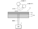
- FIG. 1 is a diagram showing the configuration of a phosphor device according to an embodiment.
- FIG. 2 is a diagram showing the configuration of the light source module according to the embodiment.
- FIG. 3 is a diagram showing the configuration of a phosphor device according to a comparative example.
- FIG. 4 is a diagram showing a table of constituent elements of the phosphor device according to the embodiment and the phosphor device according to the comparative example.
- FIG. 5 is a diagram showing the light emission characteristics of the phosphor device according to the embodiment and the phosphor device according to the comparative example.
- FIG. 6 is a cross-sectional view of the phosphor device according to Example 1.
- FIG. 1 is a diagram showing the configuration of a phosphor device according to an embodiment.
- FIG. 2 is a diagram showing the configuration of the light source module according to the embodiment.
- FIG. 3 is a diagram showing the configuration of a phosphor device according to a comparative example.
- FIG. 4 is a diagram showing
- FIG. 7 is a diagram showing the angular dependence of the chromaticity of the output light of the phosphor devices according to Study Examples 1 to 3.
- FIG. 8 is a diagram showing the angular dependence of the chromaticity of the output light of the phosphor devices according to Study Examples 4 to 6.
- FIG. 9 is a diagram showing the angular dependence of the chromaticity of the output light of the phosphor devices according to Examples 1 to 4 and Study Example 7.
- FIG. 10A is a diagram schematically showing the influence of Ce 3+ concentration and thickness on excitation light and fluorescence.
- FIG. 10B is a diagram showing the total luminous flux of the output light of nine types of samples each having a different thickness of the fluorescent part.
- FIG. 10C is a diagram showing the color temperature of nine types of samples each having a different thickness of the fluorescent part.
- FIG. 10D is a diagram showing the total luminous flux of output light of a plurality of four types of samples each having a different surface roughness of the fluorescent part.
- FIG. 11 is a diagram showing relative values of light reflectance of the first to third samples.
- FIG. 12 is a diagram showing an image showing the surface conditions of the first to third samples.
- FIG. 13 is a diagram showing luminescence images of three samples each having a different density of light reflecting portions.
- FIG. 14 is a diagram showing the area of the fluorescent part, the light-emitting area, and the value obtained by dividing the light-emitting area by the area of the fluorescent part of three samples having different densities of light-reflecting parts.
- FIG. 15 is a diagram showing an example of the light emission characteristics of three samples having different densities of light reflecting portions.
- FIG. 16 is a diagram showing another example of the light emission characteristics of three samples having different densities of light reflecting portions.
- FIG. 17 is a diagram showing relative values of light reflectance of the fourth to eighth samples.
- FIG. 18 is a diagram showing relative values of light reflectance of the 9th to 13th samples.
- FIG. 19 is a diagram showing the configuration of a phosphor device according to another example.
- each figure is a schematic diagram and is not necessarily strictly illustrated.
- symbol is attached to the substantially the same structure, and the overlapping description is omitted or simplified.
- the coefficient of linear expansion and the coefficient of linear expansion have the same meaning.
- the terms “upper” and “lower” do not refer to the upper direction (vertically upward) or the lower direction (vertically downward) in absolute spatial recognition, but are based on the stacking order in the stacked structure. Used as a term defined by the relative positional relationship. Additionally, the terms “above” and “below” are used not only when two components are spaced apart and there is another component between them; This also applies when two components are placed in close contact with each other.
- FIG. 1 is a diagram showing the configuration of a phosphor device 1 according to this embodiment.
- (a) is a top view of the phosphor device 1
- (b) is a cross-sectional view of the phosphor device 1 along line Ib-Ib in (a).
- the phosphor device 1 includes a substrate member 10 and a wavelength conversion member 20 provided on the substrate member 10.
- the substrate member 10 and the wavelength conversion member 20 are in direct thermal contact.
- the wavelength conversion member 20 is provided in direct contact with the upper surface of the substrate member 10. That is, there is no adhesive member such as an adhesive layer or a bonding member such as a bonding layer between the substrate member 10 and the wavelength conversion member 20.
- the surface of the contact surface of the substrate member 10 where the substrate member 10 contacts the wavelength conversion member 20 or the contact surface of the wavelength conversion member 20 where the wavelength conversion member 20 contacts the substrate member 10 is completely It may not be smooth.
- the substrate member 10 includes a light-transmitting base material 11, a dielectric multilayer film 12 and an antireflection film 13 provided on the light-transmitting base material 11. Further, the wavelength conversion member 20 includes a fluorescent portion 21 that emits fluorescence and a light reflecting portion 22 that reflects light.
- the light-transmitting base material 11 of the substrate member 10 is a substrate having light-transmitting properties, and has a first surface 11a (upper surface) that is a surface on the wavelength conversion member 20 side, and a second surface 11a that is opposite to the first surface 11a. It has a surface 11b (lower surface).
- the transparent base material 11 is preferably a substrate with high light transmittance.
- the light-transmitting base material 11 is preferably a transparent substrate with high transmittance to the extent that the other side can be seen through.
- the visible light transmittance of the transparent base material 11 is preferably 60% or more, more preferably 80% or more, and even more preferably 90% or more, but is not limited thereto.
- the light-transmitting base material 11 is preferably a substrate with high heat resistance.
- an alumina substrate made of Al 2 O 3 an aluminum nitride substrate made of AlN, or a gallium nitride substrate made of GaN can be used.
- the main components of the materials constituting the transparent base material 11 are Al 2 O 3 , AlN, or GaN, respectively.
- the transparent substrate having high heat resistance and light transmittance is not limited to these transparent substrates, and may be a transparent substrate such as a sapphire substrate or a glass substrate.
- the shape of the light-transmitting base material 11 is a rectangular thin plate having a length of 7.0 mm, a width of 7.0 mm, and a thickness of 1.0 mm.
- the dielectric multilayer film 12 is provided on the first surface 11a of the transparent base material 11.
- the dielectric multilayer film 12 is a surface film that is the uppermost layer of the substrate member 10.
- the dielectric multilayer film 12 has a structure in which a plurality of dielectric films are stacked, and reflects a specific light while transmitting other specific light.
- the dielectric multilayer film 12 in this embodiment reflects the light emitted by the fluorescent material of the fluorescent portion 21 of the wavelength conversion member 20 and transmits the excitation light incident on the fluorescent device 1 .
- the fluorescent section 21 is made of yellow phosphor and the excitation light that enters the phosphor device 1 is ultraviolet light or blue light
- the dielectric multilayer film 12 will reflect at least the yellow light emitted by the fluorescent section 21. , and transmits excitation light such as ultraviolet light or blue light.
- the dielectric multilayer film 12 By providing the dielectric multilayer film 12 on the first surface 11a side (wavelength conversion member 20 side) of the transparent base material 11 in this way, part of the light emitted by the fluorescent portion 21 of the wavelength conversion member 20 is absorbed into the substrate member 10.
- the dielectric multilayer film 12 can reflect the directed light. Thereby, it is possible to increase the amount of light from the fluorescent section 21 that can be taken out from the fluorescent device 1.
- the antireflection film 13 is provided on the second surface 11b of the transparent base material 11.
- the antireflection film 13 is a surface film that is the bottom layer of the substrate member 10.
- the antireflection film 13 may be either a single layer film or a multilayer film.
- the antireflection film 13 is made of silicon oxide (SiO 2 ), titanium oxide (TiO 2 ), niobium oxide (Nb 2 O 5 ), tantalum oxide (Ta 2 O 5 ), aluminum oxide (Al 2 O 3 ), It is a multilayer film in which at least two types of dielectric films such as aluminum nitride (AlN) are laminated.
- the anti-reflection film 13 By providing the anti-reflection film 13 on the second surface 11b of the transparent base material 11 in this way, light incident on the phosphor device 1 from the second surface 11b side of the transparent base material 11 is prevented from being reflected. Can be suppressed. Thereby, light that enters the light-transmitting base material 11 from the second surface 11b side of the light-transmitting base material 11 can be efficiently taken into the light-transmitting base material 11. Specifically, the excitation light that is incident on the phosphor device 1 to cause the fluorescent portion 21 to emit fluorescence can be efficiently introduced into the light-transmitting base material 11.
- the wavelength conversion member 20 is provided on the substrate member 10, and more specifically, provided above the substrate member 10.
- the fluorescent portion 21 of the wavelength conversion member 20 is a light emitting layer that emits light, and is excited by excitation light to emit fluorescent light of a predetermined wavelength in the visible light region.
- the fluorescent section 21 is a yellow phosphor layer made of yellow phosphor.
- the fluorescent section 21, which is a yellow phosphor layer emits fluorescence using light with a shorter wavelength than yellow light (for example, ultraviolet light to blue light) as excitation light. That is, in the yellow phosphor layer, the wavelength of the excitation light is converted into yellow light having a longer wavelength than the excitation light.
- the fluorescent portion 21 is a phosphor layer made only of phosphor.
- the fluorescent portion 21 is a phosphor ceramic layer made of a sintered single crystal phase phosphor, and the main component is the phosphor ceramic.
- the fluorescent section 21 is a yellow phosphor layer made of YAG (yttrium aluminum garnet) phosphor containing Ce 3+ . That is, the main component of the fluorescent part 21 is YAG phosphor ceramics containing Ce 3+ , and more specifically, the fluorescent part 21 is a member made only of YAG phosphor ceramics containing Ce 3+ . In other words, the fluorescent section 21 does not have a binder or the like.
- the Ce 3+ concentration of the YAG phosphor ceramic containing Ce 3+ that is the fluorescent part 21 is 0.005% or more and 0.02% or less.
- the fluorescent portion 21 is a phosphor ceramic layer consisting of only a single crystal phase.
- the fluorescent portion 21 includes a crystal phase having a garnet structure. More specifically, in this embodiment, the fluorescent portion 21 is composed only of a crystal phase having a garnet structure. That is, the fluorescent portion 21 according to the present embodiment does not include a crystal phase having a structure different from the garnet structure.
- the garnet structure is a crystal structure represented by the general formula A 3 B 2 C 3 O 12 .
- Rare earth elements such as Ca, Y, La, Ce, Pr, Nd, Sm, Eu, Gd, Tb and Lu are applied to element A, and rare earth elements such as Mg, Al, Si, Ga and Sc are applied to element B.
- Elements such as Al, Si, and Ga are applied to the element C.
- garnet structures include YAG, LuAG (lutetium aluminum garnet), Lu 3 Ga 2 (AlO 4 ) 3 (lutetium gallium aluminum garnet), Y 3 Ga 2 (AlO 4 ) 3 (yttrium Examples include gallium aluminum garnet), Lu 2 CaMg 2 Si 3 O 12 (lutetium calcium magnesium silicon garnet), and TAG (terbium aluminum garnet). These garnet structures are preferably used as the Ce 3+ activated phosphor.
- the material of the phosphor constituting the fluorescent portion 21 is (Y 1-x Cex ) 3 Al 2 Al 3 O 12 (that is, (Y 1-x Cex ) 3 Al 5 O 12 ) It is composed of a crystal phase expressed by (0.00005 ⁇ x ⁇ 0.0002), that is, YAG, and the fluorescent portion 21 is a fluorescent ceramic layer made only of sintered YAG.
- the fluorescent section 21 is a yellow phosphor layer made of YAG phosphor.
- the crystal phase constituting the fluorescent portion 21 may be a solid solution of a plurality of garnet crystal phases having different chemical compositions.
- a solid solution includes a garnet crystal phase represented by (Y 1-x Ce x ) 3 Al 2 Al 3 O 12 (0.00005 ⁇ x ⁇ 0.0002) and (Lu 1-d Ce d ) 3 Solid solution ( ( 1 -a)(Y 1 -x Ce x ) 3 Al 5 O 12 ⁇ a(Lu 1-d Ce d ) 3 Al 2 Al 3 O 12 (0 ⁇ a ⁇ 1)).
- such a solid solution includes a garnet crystal phase represented by (Y 1-x Ce x ) 3 Al 2 Al 3 O 12 (0.00005 ⁇ x ⁇ 0.0002) and (Lu 1-z Ce z ) 2 CaMg 2 Si 3 O 12 (0.00005 ⁇ z ⁇ 0.0002) Solid solution with garnet crystal phase ((1-b) (Y 1-x Ce x ) 3 Al 2 Al 3 O 12 ⁇ b(Lu 1-z Cez ) 2 CaMg 2 Si 3 O 12 (0 ⁇ b ⁇ 1)). Since the fluorescent part 21 is composed of a solid solution of a plurality of garnet crystal phases having different chemical compositions, the fluorescence spectrum of the fluorescence emitted by the fluorescent part 21 becomes broader, and the green light component and the red light component increase. Therefore, it is possible to provide a phosphor device 1 that emits output light with a wide color gamut.
- garnet crystal phase represented by (Y 1-x Ce x ) 3 Al 2 Al 3 O 12 (0.00005 ⁇ x ⁇ 0.0002) and (Lu 1-z Ce z )
- the crystal phase constituting the fluorescent portion 21 may include a crystal phase whose chemical composition is shifted from the crystal phase represented by the general formula A 3 B 2 C 3 O 12 described above.
- a crystal phase is an Al - rich ( Y 1 -x Ce x ) 3 Al 2+ ⁇ Al 3 O 12 ( ⁇ is a positive number).
- such a crystal phase is a Y-rich ( Examples include Y 1-x Ce x ) 3+ ⁇ Al 2 Al 3 O 12 ( ⁇ is a positive number).
- These crystal phases have different chemical compositions from the crystal phase represented by the general formula A 3 B 2 C 3 O 12 , but maintain the garnet structure. Since the fluorescent part 21 is composed of crystal phases with different chemical compositions, regions with different refractive indexes are created in the fluorescent part 21, so the excitation light and fluorescence are scattered more, and the light emitting area of the fluorescent part 21 is increased. becomes smaller.
- the following material which is a Cr 3+ activated fluorescent substance may be used.
- These materials include Y 3 Al 2 (AlO 4 ) 3 : Cr 3+ , La 3 Al 2 (AlO 4 ) 3 : Cr 3+ , Gd 3 Al 2 (AlO 4 ) 3 : Cr 3+ , Y 3 Ga 2 (AlO 4 ) 3 : Cr 3+ , La 3 Ga 2 (AlO 4 ) 3 : Cr 3+ , Gd 3 Ga 2 (AlO 4 ) 3 : Cr 3+ , Y 3 Sc 2 (AlO 4 ) 3 : Cr 3+ , La 3 Sc 2 (AlO 4 ) 3 : Cr 3+ , Gd 3 Sc 2 (AlO 4 ) 3 : Cr 3+ , Y 3 Ga 2 (GaO 4 ) 3 : Cr 3+ , La 3 Ga 2 (GaO 4 ) 3 : Cr 3+ , (Gd , La 3 Ga 2 (GaO 4
- the density of the fluorescent part 21 (that is, the density of the YAG phosphor ceramics) may be 90% or more and 100% or less of the theoretical density, preferably 95% or more and 100% or less of the theoretical density, and 98% of the theoretical density. It is even better if it is % or more and 100% or less.
- the theoretical density is the density assuming that the atoms in the layer are ideally arranged.
- the theoretical density is the density assuming that there are no voids in the fluorescent part 21, and is a value calculated using the crystal structure.
- the density of the fluorescent portion 21 is 99%, the remaining 1% corresponds to voids. In other words, the higher the density of the fluorescent portions 21, the fewer voids there are.
- the density of the fluorescent portions 21 is within the above range, the total amount of fluorescent light emitted by the fluorescent portions 21 increases, so it is possible to provide a phosphor device 1 that emits a larger amount of light.
- the density of the fluorescent portion 21 may be 4.10 g/cm 3 or more and 4.55 g/cm 3 or less, more preferably 4.32 g/cm 3 or more and 4.55 g/cm 3 or less, and 4. It is even better if it is 46 g/cm 3 or more and 4.55 g/cm 3 or less.
- the density of the fluorescent part 21 is 90% or more and 100% or less of the theoretical density, respectively. 95% or more and 100% or less and 98% or more and 100% or less.
- the excitation light absorbed by the fluorescent portion 21 can be efficiently converted into fluorescence. In other words, the fluorescent section 21 with high luminous efficiency is realized.
- the top view shape of the fluorescent section 21 is rectangular, but is not limited to this.
- the top view shape of the fluorescent portion 21 may be circular.
- the top view shape of the fluorescent section 21 is a rectangle measuring 0.8 mm in length and 0.8 mm in width.
- the thickness of the fluorescent portion 21 (that is, the thickness of the YAG phosphor ceramic) is 350 ⁇ m or more and 820 ⁇ m or less. This thickness is sufficiently thick, so that heat dissipation from the side surfaces of the fluorescent section 21 can be ensured. Note that the thickness of the fluorescent portion 21 is constant, but is not limited to this. Note that the thickness of the fluorescent portion 21 may be 350 ⁇ m or more and 805 ⁇ m or less, or 400 ⁇ m or more and 805 ⁇ m or less.
- the fluorescent section 21 has a light entrance surface 211, a light exit surface 212, and side surfaces (four side surfaces 213 to 216).
- the light incidence surface 211 is a surface onto which excitation light for exciting the fluorescent section 21 is incident, and is the lower surface of the fluorescent section 21 .
- the light emitting surface 212 is a surface from which the fluorescent section 21 emits fluorescent light, and is the upper surface of the fluorescent section 21 .
- the light entrance surface 211 and the light exit surface 212 are surfaces facing each other.
- the four side surfaces 213 to 216 are lateral surfaces of the fluorescent section 21. Each of the four side surfaces 213 to 216 is a plane perpendicular to the light entrance surface 211 and the light exit surface 212.
- the two side surfaces 213 and 215 are opposite surfaces, and the two side surfaces 214 and 216 are opposite surfaces.
- the light reflecting section 22 of the wavelength conversion member 20 is provided around the fluorescent section 21 when viewed from the direction of the light output surface 212, that is, when viewed from above.
- the light reflecting section 22 surrounds the entire periphery of the fluorescent section 21 when viewed from above.
- the light reflecting section 22 is in contact with all the four side surfaces 213 to 216 of the fluorescent section 21.
- the fluorescent section 21 has a rectangular shape when viewed from above
- the light reflecting section 22 has a rectangular opening.
- the shape of the light reflecting section 22 when viewed from above is a rectangular frame having a rectangular opening and a rectangular outer shape.
- the top view shape of the light reflecting section 22 is not limited to a rectangular frame shape, but may be an annular shape or the like.
- the outer shape of the light reflecting section 22 when viewed from above is 7.0 mm long x 7.0 mm wide.
- the thickness of the light reflection part 22 and the thickness of the fluorescent part 21 are the same, but are not limited to this.
- the light reflecting section 22 is in thermal contact with the fluorescent section 21. That is, the fluorescent section 21 and the light reflecting section 22 are provided so that the heat generated in the fluorescent section 21 can be conducted to the light reflecting section 22.
- the light reflecting section 22 is physically in contact with the fluorescent section 21. Specifically, the entire inner circumferential side surface of the light reflecting section 22 is in contact with the outer circumferential side surface of the fluorescent section 21 . That is, the fluorescent section 21 is provided so as to fill the opening of the light reflecting section 22.
- the thickness (height) of the light reflection section 22 is the same as the thickness (height) of the fluorescent section 21, it is not limited thereto. That is, the thickness of the light reflecting section 22 may be lower than the thickness of the fluorescent section 21 or may be higher than the thickness of the fluorescent section 21. However, it is preferable that the light reflecting section 22 be provided so as not to cover the upper surface of the fluorescent section 21 . That is, the light reflecting section 22 is preferably formed so that the material (such as a binder) constituting the light reflecting section 22 does not protrude onto the upper surface of the fluorescent section 21 .
- the main component of the light reflecting portion 22 is light reflective ceramics, and the main component of the light reflective ceramics is alumina ceramics. That is, here, the light reflecting portion 22 is constituted by a ceramic layer made of a ceramic material such as alumina (aluminum oxide (Al 2 O 3 )). More specifically, the light reflecting portion 22 is an alumina ceramic layer made only of alumina. In other words, the light reflecting section 22 does not include a binder or the like. In this embodiment, the light reflecting section 22 is white because it reflects light having a wavelength in the visible light band. In other words, the light reflecting section 22 is a white ceramic layer. Note that the light reflecting portion 22 does not need to be made of ceramics as long as it has the function of reflecting visible light. For example, the light reflecting portion 22 may be made of white resin or metal containing light reflective particles. It may be.
- the light reflecting section 22 that is, light reflecting ceramics
- the light reflecting section 22 is a ceramic layer
- the density of the light-reflecting portion 22 (that is, the density of the light-reflecting ceramic) may be 98% or less of the theoretical density, better if it is 95% or less, and even better if it is 90% or less.
- the fluorescent section 21 in this embodiment is a phosphor ceramic layer made of only sintered phosphor, and the light reflecting section 22 is a ceramic layer made of alumina ceramics. This facilitates integration of the fluorescent section 21 and the light reflecting section 22.
- FIG. 2 is a diagram showing the configuration of light source module 100 according to this embodiment.
- the light source module 100 includes a phosphor device 1 and a light source 2 that emits light that is incident on the phosphor device 1.
- the light source module 100 is used, for example, as a light emitting device included in an endoscope.
- the light source 2 is an excitation light source that emits excitation light for causing the fluorescent portion 21 of the wavelength conversion member 20 to emit light.
- the phosphor included in the fluorescent part 21 is excited by the excitation light emitted from the light source 2 and emits fluorescence.
- the light source module 100 is a transmission type light emitting device in which excitation light incident on the phosphor device 1 is transmitted through the phosphor device 1 . That is, the excitation light incident on the phosphor device 1 is transmitted through the wavelength conversion member 20. Therefore, the light source 2 is arranged such that the light emitted by the light source 2 is transmitted through the phosphor device 1. Specifically, the light source 2 is arranged below the phosphor device 1 (on the substrate member 10 side).
- the light source 2 for example, a semiconductor laser that emits ultraviolet or blue laser light can be used. Since laser light has excellent straightness, by using a semiconductor laser as the light source 2, the laser light (excitation light) can be made to enter the fluorescent section 21 at a desired angle of incidence.
- the light source 2 is not limited to a semiconductor laser, and may be another solid-state light emitting device such as an LED, or an excitation light source other than a solid-state light emitting device.
- the light source module 100 configured in this way, when the light emitted from the light source 2 enters the phosphor device 1, output light of a predetermined color is emitted from the phosphor device 1. More specifically, output light of a predetermined color is emitted from the light exit surface 212 of the fluorescent section 21 .
- the light (excitation light) emitted from the light source 2 is incident on the back surface of the substrate member 10.
- the light (excitation light) from the light source 2 that has entered the substrate member 10 passes through the substrate member 10 and reaches the fluorescent portion 21 of the wavelength conversion member 20 . That is, the excitation light emitted from the light source 2 enters the fluorescent section 21 from the light incident surface 211 of the fluorescent section 21.
- the external size of the fluorescent section 21 is preferably equal to the spot size (spot size of excitation light) when the light emitted from the light source 2 enters the fluorescent section 21 .
- the excitation light of the light source 2 is blue light
- the fluorescent section 21 is a yellow phosphor layer.
- the blue light from the light source 2 enters the fluorescent section 21 .
- the yellow phosphor (YAG phosphor) of the fluorescent section 21 absorbs a portion of the blue light from the light source 2, is excited, and emits yellow light as fluorescence.
- this yellow light and the blue light from the light source 2 that is not absorbed by the yellow phosphor are mixed to become white light, and this white light is emitted from the fluorescent section 21 as output light. That is, output light (white light) is extracted from the wavelength conversion member 20.
- a dielectric multilayer film 12 is formed on the substrate member 10.
- the dielectric multilayer film 12 reflects yellow light emitted by the fluorescent section 21 and transmits blue light, which is excitation light. With this configuration, of the yellow light emitted by the fluorescent section 21, the light directed toward the light source 2 is reflected by the dielectric multilayer film 12 and travels toward the opposite side from the light source 2.
- a white light reflecting section 22 is formed around the fluorescent section 21.
- the output light (white light) emitted from the fluorescent section 21 the light traveling in the horizontal direction is reflected by the light reflecting section 22, returns to the fluorescent section 21, and is emitted from the fluorescent section 21 to the outside. be done. Thereby, it is possible to increase the amount of light that can be extracted from the fluorescent section 21.
- the phosphor device 1 is of a remote phosphor type, and the phosphor device 1 and the light source 2 are arranged spatially apart. Thereby, it is possible to suppress the influence of the heat generated by the light source 2 on the phosphor device 1 (especially the phosphor section 21).
- the light emitted from the light source 2 is incident perpendicularly to the back surface of the substrate member 10, but it may be incident obliquely to the back surface of the substrate member 10.
- a light guide (not shown) is provided above the phosphor device 1, and the output light incident on this light guide is used for the endoscope. Used as light. The more light that is incident on the light guide among the output light output from the phosphor device 1, the higher the utilization efficiency of the output light.
- the light guide is an optical member composed of a lens, a rod integrator, and the like.
- the light source module 100 is a white light source module.
- FIG. 3 is a diagram showing the configuration of a phosphor device 1x according to a comparative example.
- the phosphor device 1x includes a substrate member 10 and a wavelength conversion member 20x arranged above the substrate member 10. Further, the wavelength conversion member 20x includes a fluorescent portion 25x and a binder 26x.
- FIG. 4 is a diagram showing a table of constituent elements of the phosphor device 1 according to the present embodiment and the phosphor device 1x according to the comparative example.
- the wavelength conversion member 20x included in the phosphor device 1x according to the comparative example does not have the light reflection section 22, unlike the wavelength conversion member 20 according to the embodiment. Furthermore, the density of the light reflecting portions 22 included in the wavelength conversion member 20 according to the embodiment is 81.1% of the theoretical density, as shown in FIG.
- the light emitting area is approximately 0.34 mm 2 in the comparative example, and approximately 0.64 mm 2 (0.8 mm ⁇ 0.8 mm) in the embodiment.
- the fluorescent portion 25x is a fluorescent particle, more specifically, a fluorescent particle made of YAG.
- the binder 26x is a material for holding the fluorescent portion 25x and adhering it above the substrate member 10, and is, for example, transparent ZnO crystal.
- the refractive index of the wavelength conversion member 20x consisting of the fluorescent portion 25x and the binder 26x is approximately 1.95, and the refractive index of the fluorescent portion 21 is 1.83.
- the Ce 3+ concentration in YAG constituting the fluorescent section 25x according to the comparative example is about 0.1%, and the Ce 3+ concentration in YAG constituting the fluorescent section 21 according to the embodiment is 0.01%.
- the thickness of the wavelength conversion member 20x according to the comparative example is about 20 ⁇ m, and the thickness of the fluorescent section 21 according to the embodiment is 500 ⁇ m or more and 700 ⁇ m or less. Further, the density of the fluorescent portion 21 is 98.8% of the theoretical density.
- the luminance distribution when the excitation light is irradiated is shown as a gradation.
- the entire fluorescent section 21 that is, the entire 0.64 mm 2 of 0.8 mm x 0.8 mm
- FIG. 5 is a diagram showing the light emission characteristics of the phosphor device 1 according to the present embodiment and the phosphor device 1x according to the comparative example.
- the horizontal axis in FIG. 5 indicates the power input to emit excitation light from the light source 2 (input power).
- the vertical axis in FIG. 5 indicates the total luminous flux of light that enters the light guide provided above the phosphor device 1 and the phosphor device 1x and exits from the light guide.
- the light emitted from this light guide may be described as light guide light.
- the total luminous flux of the light guide light based on the output light output from the phosphor device 1 is the total luminous flux of the light guide light based on the output light output from the phosphor device 1x. higher than the luminous flux.
- the total luminous flux of the light guide light based on the output light output from the phosphor device 1 is the total luminous flux of the light guide light based on the output light output from the phosphor device 1x. It's about 30% higher than that.
- the total luminous flux of the light guide light based on the output light output from the phosphor device 1 is equal to the total luminous flux of the light guide light based on the output light output from the phosphor device 1x. It is about 46% higher than the total luminous flux.
- the factors why the phosphor device 1 according to the present embodiment has higher light emission characteristics than the phosphor device 1x according to the comparative example will be described below.
- the phosphor device 1 is provided with a light reflecting section 22. Therefore, among the output light (white light) emitted from the fluorescent section 21, the light traveling in the horizontal direction is reflected by the light reflecting section 22, returns to the fluorescent section 21, and is emitted from the fluorescent section 21 to the outside. Ru. That is, out of the output light (white light) emitted from the fluorescent section 21, the light that travels in the horizontal direction is suppressed from becoming unusable light. Therefore, the total luminous flux of the light guide light based on the output light output from the phosphor device 1 becomes higher.
- a phosphor ceramic layer is used as the phosphor portion 21. Therefore, the heat resistance and heat dissipation of the fluorescent section 21 can be improved, and the luminous efficiency of the fluorescent section 21 is less likely to decrease due to heat. In particular, if the density of the fluorescent portion 21 (that is, the density of the YAG phosphor ceramic) is within the above range, the luminous efficiency of the fluorescent portion 21 is less likely to decrease due to heat. Further, by using a phosphor ceramic layer as the fluorescent part 21, it is possible to suppress light loss due to scattering of fluorescence, and thus the conversion efficiency of the fluorescent part 21 can be improved. Therefore, the total luminous flux of the light guide light based on the output light output from the phosphor device 1 becomes higher.
- the phosphor device 1 according to the present embodiment has higher light emission characteristics than the phosphor device 1x according to the comparative example.
- FIG. 6 is a cross-sectional view of the phosphor device 1a according to Example 1.
- the phosphor device 1a includes a substrate member 10a and a phosphor section 21a.
- the substrate member 10a has a structure in which the antireflection film 13 is removed from the substrate member 10, and in other words, it has a transparent base material 11 and a dielectric multilayer film 12 provided on the transparent base material 11. are doing.
- the fluorescent part 21a included in the phosphor device 1a is a fluorescent part 21a, except that it is provided in contact with the upper part of the dielectric multilayer film 12 and that no light reflecting part 22 is provided around it. It has the same configuration as the fluorescent section 21 included in the device 1.
- the Ce 3+ concentration is 0.01% and the thickness is 705 ⁇ m.
- each of the phosphor devices according to Study Examples 1 to 7 and Examples 2 to 4 has the same configuration as the phosphor device 1a except for the Ce 3+ concentration and thickness of the fluorescent portion. More specifically, the Ce 3+ concentration and thickness of the fluorescent part are 0.08% and 225 ⁇ m in Study Example 1, 0.08% and 125 ⁇ m in Study Example 2, and 0.08% and 57 ⁇ m in Study Example 3, respectively. It is. Further, the Ce 3+ concentration and thickness of the fluorescent part are 0.03% and 666 ⁇ m in Study Example 4, 0.03% and 400 ⁇ m in Study Example 5, and 0.03% and 300 ⁇ m in Study Example 6, respectively. In addition, the Ce 3+ concentration and thickness of the fluorescent part are 0.01% and 659 ⁇ m in Example 2, 0.01% and 400 ⁇ m in Example 3, 0.01% and 805 ⁇ m in Example 4, and Study Example 7. 0.01% and 300 ⁇ m.
- the phosphor devices according to Examples 1 to 4 correspond to the phosphor device 1 according to the present embodiment in terms of Ce 3+ concentration and thickness.
- Table 1 shows the target composition, raw materials used, and raw material blending ratio of the phosphor parts (YAG phosphor ceramics) used in the phosphor devices according to Study Examples 1 to 7 and Examples 1 to 4. This is a table.
- each raw material shown in Table 1 was placed in a plastic pot (hereinafter referred to as pot) with a volume of 1 L. At this time, each raw material used and an alumina ball ( ⁇ 10 mm) were put into the pot. The amount of alumina balls was set to fill approximately 1/3 of the volume of the pot.
- Ball mill mixing was performed for 12 hours using a pot rotating device (BALL MILL ANZ-51S, manufactured by Nichito Kagaku Co., Ltd.).
- the slurry-like mixed raw materials were dried using a dryer after ball mill mixing. Specifically, the above mixed raw material was poured onto a Naflon (registered trademark) sheet (thickness: 0.05 mm) spread over the inner wall of a metal bat, and the mixed raw material was placed in a dryer set at 150°C. for 6 hours to dry.
- a Naflon (registered trademark) sheet thinness: 0.05 mm
- the dried mixed raw materials were collected and granulated using a mortar and pestle. Specifically, the mixed raw material after drying was put into a mortar and ground to obtain a mixed raw material powder. Furthermore, 0.18 mL of a binder liquid (5 wt.% PVA (polyvinyl alcohol) solution) was added little by little to 10 g of mixed raw material powder using a pipette, and kneaded using a pestle. In other words, the binder liquid was dispersed throughout the mixed raw material powder. Thereafter, the mixed raw material powder was classified using a nylon mesh to obtain granulated powder. Note that the opening diameter of the nylon mesh was 155 ⁇ m. In this way, raw materials for powdered fluorescent parts (YAG phosphor ceramics) for Study Examples 1 to 7 and Examples 1 to 3 were obtained.
- a binder liquid 5 wt.% PVA (polyvinyl alcohol) solution
- Example 4 after ball mill mixing, the slurry-like mixed raw materials were granulated using a spray dryer device. More specifically, 0.5wt. % of a binder (for example, PVA (polyvinyl alcohol)) was added to the slurry-like mixed raw material, which was granulated using a spray dryer device. The average particle diameter of the obtained granulated powder was 45 ⁇ m. In this way, a raw material for the powdered fluorescent part (YAG fluorescent ceramics) for Example 4 was obtained.
- a binder for example, PVA (polyvinyl alcohol)
- each raw material was molded into a cylindrical shape using a manual hydraulic press machine (manufactured by Riken Seiki Co., Ltd.) and a mold ( ⁇ 13 mm).
- the pressure applied to the sample during mold molding was 6 MPa.
- the raw material was actually molded using a cold isostatic press (CIP) device.
- the pressure during main molding was 250 MPa.
- the molded body after this molding was subjected to binder removal treatment (heat treatment in the air) for the purpose of removing the adhesive (polyvinyl alcohol) used during granulation.
- the conditions for the binder removal treatment were 500° C. and 10 hours.
- Example 4 The raw material for Example 4 was molded in the same manner as the raw materials for Study Examples 1 to 7 and Examples 1 to 3, except for one point below.
- the one point is that a mold ( ⁇ 60 mm) was used when a manual hydraulic press machine (manufactured by Riken Seiki Co., Ltd.) was used.
- each molded body was fired using a vertical tubular atmosphere furnace.
- the firing temperature was 1725°C.
- the firing time was 4 hours.
- the firing atmosphere was 97vol. % nitrogen and 3 vol. % hydrogen as a mixed gas. Further, the flow rate of the mixed gas was 1 L/min.
- Example 4 firing in Example 4 will be explained.
- the raw material for Example 4 after the binder removal treatment was fired using a vertical tubular atmosphere furnace under the following conditions.
- the conditions are that the firing temperature is 1700°C or more and 1725°C or less, the firing time is 4 hours or more and 24 hours or less, and the firing atmosphere is 95 vol. % or more 97vol. % nitrogen and 3 vol. % or more 5vol. % or less of hydrogen, and the flow rate of the mixed gas is 1 L/min or more and 5 L/min or less.
- each sample was mirror-polished using a polishing device (DFD6340, manufactured by DISCO Co., Ltd.).
- the thickness after mirror polishing was set to three levels: 225 ⁇ m (examination example 1), 125 ⁇ m (examination example 2), and 57 ⁇ m (examination example 3) for samples with a Ce 3+ concentration of 0.08%.
- Samples with a Ce 3+ concentration of 0.03% had three levels: 666 ⁇ m (Study Example 4), 400 ⁇ m (Study Example 5), and 300 ⁇ m (Study Example 6).
- the samples with a Ce 3+ concentration of 0.01% were 705 ⁇ m (Example 1), 659 ⁇ m (Example 2), 400 ⁇ m (Example 3), 805 ⁇ m (Example 4), and 300 ⁇ m (Study Example 7). It was set as 4 levels.
- each sample was diced using a dicing device (DAD3350, manufactured by Disco Corporation).
- DAD3350 manufactured by Disco Corporation.
- the samples of Study Examples 1 to 7 and Examples 1 to 3 were diced into squares with sides of 7 mm, and the samples of Example 4 were diced into squares with sides of 10 mm.
- fluorescent parts according to Study Examples 1 to 7 and Examples 1 to 4 were manufactured.
- the density of each fluorescent part was evaluated using the Archimedes method. Then, assuming the theoretical density of YAG to be 4.55 g/cm 3 , the ratio of each fluorescent part to the theoretical density was calculated.
- the chromaticity of the output light in the direction was measured by a spectrometer. Note that the output light output in the 0° direction and the 45° direction corresponds to the light that enters the above-mentioned light guide. More specifically, the chromaticity of the output light was measured as follows.
- each sample after dicing was placed above the substrate member 10a, and phosphor devices according to Study Examples 1 to 7 and Examples 1 to 4 were fabricated.
- Each of the phosphor devices according to Study Examples 1 to 7 and Examples 1 to 4 is irradiated with a 0.83 W laser beam from the light source 2 from the substrate member 10a side.
- the laser beam irradiation spot area was 4 mm 2 .
- the transparent base material 11 is a sapphire substrate, and has a rectangular shape of 7 mm x 7 mm for the samples of Study Examples 1 to 7 and Examples 1 to 3, and
- the sample has a rectangular shape of 10 mm x 10 mm and a thickness of 500 ⁇ m.
- the dielectric multilayer film 12 is a film that transmits blue light and reflects light in a wavelength range of 480 nm or more and 780 nm or less with a reflectance of 90% or more.
- the angular dependence of the chromaticity of the output light output from each of the phosphor devices according to Study Examples 1 to 7 and Examples 1 to 4 was measured by irradiation with laser light.
- Each of the output lights was measured using an integrating sphere (manufactured by Nemtech Co., Ltd.) and a multichannel spectrometer (manufactured by Otsuka Electronics Co., Ltd., MCPD-7000). Note that here, each phosphor device is not provided with a light reflecting section. However, the chromaticity of the output light and the angular dependence of the chromaticity of the output light are presumed to be the same as in the case where a light reflecting section is provided.
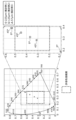
- FIG. 7 is a diagram showing the angular dependence of the chromaticity of the output light of the phosphor devices according to Study Examples 1 to 3.
- FIG. 8 is a diagram showing the angular dependence of the chromaticity of the output light of the phosphor devices according to Study Examples 4 to 6.
- FIG. 9 is a diagram showing the angular dependence of the chromaticity of the output light of the phosphor devices according to Examples 1 to 4 and Study Example 7.
- FIGS. 7 to 9 xy chromaticity diagrams are shown in FIGS. 7 to 9, and the chromaticity of output light of each phosphor device in the 0° direction and 45° direction is shown in the xy chromaticity diagram.
- FIGS. 7 to 9 a rectangular chain line showing a part of the xy chromaticity diagram is shown enlarged.
- FIGS. 7 to 9 a rectangular broken line is shown, and this broken line indicates the permissible chromaticity range when a light source module including a phosphor device is used in an endoscope, for example. .
- the light source module is used for an endoscope, both the output light in the 0° direction and the output light in the 45° direction are used as light for the endoscope. Therefore, if both the chromaticity in the 0° direction and the chromaticity in the 45° direction fall within this chromaticity range (rectangular broken line), it is determined that the light source module can be used as a light emitting device for an endoscope. be done.
- a light source module including a phosphor device with a small angular dependence of chromaticity of output light has higher performance as a light emitting device for an endoscope.
- Table 2 is a table showing the xy coordinates of the chromaticity of the output light of the phosphor devices according to Study Examples 1 to 3.
- Table 3 is a table showing the xy coordinates of the chromaticity of the output light of the phosphor devices according to Study Examples 4 to 6.
- Table 4 is a table showing the xy coordinates of the chromaticity of the output light of the phosphor devices according to Examples 1 to 4 and Study Example 7.
- the chromaticity in the 0° direction and the chromaticity in the 45° direction are within the chromaticity range (rectangular broken line); It is clear that the difference with the chromaticity in the ° direction is very large. On the other hand, in all of the phosphor devices according to Examples 1 to 4, the difference between the chromaticity in the 0° direction and the chromaticity in the 45° direction is very small, which means that the angular dependence of chromaticity is is shown to be small.
- the phosphor device according to Examination Example 6 see FIG. 8
- the phosphor device according to Example 2 see FIG. 9
- the angular dependence of chromaticity in the phosphor device according to Example 2 is smaller than the angular dependence of chromaticity in the phosphor device according to Study Example 6.
- the phosphor device according to Example 2 in which the Ce 3+ concentration in the fluorescent portion is sufficiently low, has been shown to have smaller angular dependence of chromaticity.
- the Ce 3+ concentration is 0.01% and the thickness is 350 ⁇ m or more and 820 ⁇ m or less, so that the chromaticity of the output light is lower than in Examples 1 to 7.
- a phosphor device with small angular dependence has been realized. This principle will be explained using FIG. 10A.
- FIG. 10A is a diagram schematically showing the influence of Ce 3+ concentration and thickness on excitation light and fluorescence.
- FIG. 10A a fluorescent part with a changed Ce 3+ concentration and thickness, and excitation light (blue light) and fluorescence (yellow light) reaching the fluorescent part are schematically shown.
- the ratio of the lengths of the solid line arrow indicating blue light and the broken line arrow indicating yellow light indicates the ratio of the blue light intensity and yellow light intensity in the output light.
- the fluorescent portion having a high Ce 3+ concentration and a thick thickness corresponds to Study Example 4, and the fluorescent portion having a high Ce 3+ concentration and a thin thickness corresponds to Study Example 6. Further, the fluorescent portion having a low Ce 3+ concentration and a thick thickness corresponds to Example 2, and the fluorescent portion having a low Ce 3+ concentration and a thin thickness corresponds to Study Example 7.
- Example 2 the intensity of the yellow light is lower in the 0° direction and the 45° direction than in Examination Example 6, so the output light becomes light close to white. Further, since the difference in the ratio of the length of the solid line arrow (blue light) to the length of the broken line arrow (yellow light) is small between the 0° direction and the 45° direction, the angular dependence of chromaticity is small.
- the phosphor devices according to Examples 1 to 4 correspond to the phosphor device 1 according to the present embodiment in terms of Ce 3+ concentration and thickness. Therefore, like the phosphor devices according to Examples 1 to 4, the phosphor device 1 according to the present embodiment has chromaticity in the 0° direction and 45° direction within the chromaticity range, and This results in a phosphor device with small angular dependence.
- the thickness of the fluorescent part 21 of the six types of samples is 350 ⁇ m or more and 820 ⁇ m or less.
- the designed thicknesses of the fluorescent portions 21 in the six types of samples are 575 ⁇ m, 641 ⁇ m, 680 ⁇ m, 747 ⁇ m, 753 ⁇ m, and 802 ⁇ m, respectively.
- a sample with a designed thickness of the fluorescent part 21 is 575 ⁇ m
- a sample with a design thickness of 641 ⁇ m is a sample of 641 ⁇ m
- a sample with a design thickness of 680 ⁇ m is a sample of 680 ⁇ m
- a sample with a design thickness of 747 ⁇ m is a sample of 747 ⁇ m
- a sample with a design thickness of 753 ⁇ m is a sample of 753 ⁇ m.
- a sample having a diameter of 802 ⁇ m may be described as sample 802 ⁇ m.
- the remaining three types of samples among the nine types of samples have the same configuration as the phosphor device 1 shown in FIG. 1 except that the thickness of the fluorescent part is different.
- the thickness of the section is greater than 820 ⁇ m.
- the designed thicknesses of the fluorescent parts in the three types of samples are 826 ⁇ m, 873 ⁇ m, and 918 ⁇ m.
- a sample with a designed thickness of the fluorescent portion of 826 ⁇ m may be referred to as a sample 826 ⁇ m, a sample with a design thickness of 873 ⁇ m as a sample 873 ⁇ m, and a sample with a design thickness of 918 ⁇ m as a sample 918 ⁇ m.
- YAG phosphor ceramics were produced to be used in the fluorescent parts of each of the nine types of samples.
- the target composition of the YAG phosphor ceramic used in the fluorescent part was the same as that of the YAG phosphor ceramic used in the phosphor devices of Examples 1 to 4 and Study Example 7. Further, the YAG phosphor ceramic used in the phosphor section was manufactured by the same method as the YAG phosphor ceramic used in the phosphor device of Example 4 up to the step of firing (firing step).
- the YAG phosphor ceramics that have been subjected to the firing process are then processed using a polishing device (manufactured by DISCO Co., Ltd., DFD6340) and a dicing device (manufactured by DISCO Co., Ltd., DAD3350) to a size of 0.8 mm in length and 0.8 mm in width.
- the shape was processed so that the height was 0.8 mm and the height was 1 mm or more.
- a mold ( ⁇ 13 mm) was prepared, and Al 2 O 3 powder having an average primary particle diameter of 0.28 ⁇ m was charged into the mold.
- the shaped YAG phosphor ceramics were then placed into the Al 2 O 3 powder that filled the mold.
- the shaped YAG phosphor ceramic was placed near the center of the Al 2 O 3 powder filling the mold so that its height direction was substantially perpendicular to the ground. Then, using a manual hydraulic press machine (manufactured by Riken Seiki Co., Ltd.), it was molded into a substantially cylindrical shape. The pressure applied to the sample during mold molding was 6 MPa. Next, main molding was performed using a cold isostatic press (CIP) device. The pressure during main molding was 250 MPa. In this way, a composite molded body was produced in which the shaped YAG phosphor ceramic was placed in Al 2 O 3 powder. The produced composite molded body was fired using a box-type atmospheric furnace. The firing temperature was 1200°C to 1300°C.
- the firing time was 2 hours.
- a composite ceramic consisting of shaped YAG phosphor ceramics and Al 2 O 3 ceramics was produced.
- the produced composite ceramics were changed into nine different thicknesses using a polishing device (DFD6340, manufactured by DISCO Co., Ltd.).
- DMD6340 manufactured by DISCO Co., Ltd.
- Each of the nine types of composite ceramics with different thicknesses was diced using a dicing device (DAD3350, manufactured by DISCO Co., Ltd.) to a length of 7.0 mm so that the YAG phosphor ceramic was placed approximately in the center. It was shaped into a square with a width of 7.0 mm.
- sample 575 ⁇ m, sample 641 ⁇ m, sample 680 ⁇ m, sample 747 ⁇ m, sample 753 ⁇ m, and sample 802 ⁇ m are phosphor devices having the same configuration as phosphor device 1 shown in FIG. It is.
- These nine types of samples are samples in which the thickness of the fluorescent portion (thickness in the vertical direction in FIG. 1) has been changed. The total luminous flux of output light output from each of the nine types of samples was measured.
- FIG. 10B is a diagram showing the total luminous flux of the output light of nine types of samples each having a different thickness of the fluorescent part.
- the total luminous flux of the output light of each of the nine types of samples is measured when the power input to emit the excitation light is 5.2 W.
- Table 5 is a table showing the thickness of the fluorescent part and the total luminous flux of output light of nine types of samples.
- the total luminous flux of the output light output from the nine types of samples is all 930 lm or more, and more specifically, 1200 lm or more. Furthermore, it has been shown that the thicker the fluorescent part is, the higher the total luminous flux tends to be.
- the total luminous flux of the output light output from the phosphor device 1 should be 930 lm or more. is required.
- Six types of samples that is, sample 575 ⁇ m, sample 641 ⁇ m, sample 680 ⁇ m, sample 747 ⁇ m, sample 753 ⁇ m, and sample 802 ⁇ m) in which the thickness of the fluorescent portion 21 is 350 ⁇ m or more and 820 ⁇ m or less are the fluorescence according to the present embodiment as described above.
- the samples correspond to the body device 1, and the total luminous flux of the output light of the six types of samples is all 930 lm or more.
- the phosphor device 1 (each of the six types of samples) is a device with a high total luminous flux of output light to the extent that it can be used in an endoscope.
- the three types of samples in which the thickness of the fluorescent part is larger than 820 ⁇ m are also samples with a high total luminous flux of output light to the extent that they can be used in an endoscope from the viewpoint of total luminous flux.
- the phosphor device 1 is a fluorescent material whose chromaticity in the 0° direction and the 45° direction falls within the chromaticity range, and whose angular dependence of chromaticity is small. It is shown that it is a body device. Therefore, in this embodiment, the Ce 3+ concentration is 0.01% and the thickness is 350 ⁇ m or more and 820 ⁇ m or less, so that the angular dependence of the chromaticity of the output light is small and the total luminous flux of the output light is A high quality phosphor device 1 has been realized.
- FIG. 10C is a diagram showing the color temperature of nine types of samples each having a different thickness of the fluorescent part. Further, in FIG. 10C, an approximate straight line calculated by the least squares method based on the color temperatures of nine types of samples is shown as a dashed-dotted line.
- Table 6 is a table showing the thickness of the fluorescent part and the color temperature of the output light of nine types of samples.
- the color temperature of the output light output from the phosphor device 1 is 3500K or more and 15000K or less.
- a range of 4500K or more and 7000K or less is better, and a range of 5050K or more and 5810K or less is even more suitable.
- Three types of samples that is, sample 747 ⁇ m, sample 753 ⁇ m, and sample 802 ⁇ m) in which the thickness of the fluorescent portion 21 is 747 ⁇ m or more and 802 ⁇ m or less are samples corresponding to the phosphor device 1 according to the present embodiment as described above. .
- the color temperatures of the output light of the three types of samples are all 5050K or more and 5810K or less, that is, the values are within the above-mentioned more suitable range. Further, when calculated using the approximate straight line in FIG. 10C, it is estimated that if the sample has a fluorescent portion with a thickness in the range of 726 ⁇ m or more and 902 ⁇ m or less, the color temperature will be a value within the above-mentioned more suitable range. Note that, as explained in FIG. 10A and the like, the color temperature changes due to a change in the thickness of the fluorescent part.
- the thickness of the phosphor portion 21 is 726 ⁇ m or more and 820 ⁇ m or less, the color temperature of the output light is in a more suitable range. , and the angular dependence of the chromaticity of the output light is small, as shown in FIG. Therefore, the phosphor device 1 according to this embodiment can be more easily used in endoscopes.
- the thickness of the fluorescent portion 21 is not limited to the above, and may be 750 ⁇ m or more and 820 ⁇ m or less, 770 ⁇ m or more and 820 ⁇ m or less, or 790 ⁇ m or more and 820 ⁇ m or less.
- YAG phosphor ceramics to be used for the fluorescent portions 21 of each of the four types of samples were manufactured.
- the target composition of the YAG phosphor ceramic used in the phosphor section 21 was the same as that of the YAG phosphor ceramic used in the phosphor devices of Examples 1 to 4 and Study Example 7.
- the YAG phosphor ceramic used in the phosphor section 21 is different from the YAG phosphor ceramic used in the phosphor devices of Examples 1 to 3 and Study Example 7 until the firing step (firing step). Made using the same method.
- FIG. 10D is a diagram showing the total luminous flux of output light of four types of samples whose fluorescent parts 21 have different surface roughnesses.
- the total luminous flux of the output light of each of the four types of samples is measured when the power input to emit the excitation light is 5.2 W.
- sample (1400/8000) A sample (hereinafter referred to as sample (1400/8000)) was prepared in which the light exit surface 212 was polished with a grindstone grain size of No. 1400 and the light incidence surface 211 was polished with a grindstone grain size of No. 8000.
- sample (600/600) A sample (hereinafter referred to as sample (600/600)) was prepared in which the light exit surface 212 was polished with a grindstone grain size of No. 600 and the light incidence surface 211 was polished with a grindstone grain size of No. 600.
- sample (1400/1400) was prepared in which the light exit surface 212 was polished with a grindstone grain size of No.
- sample 4000/4000 A sample (hereinafter referred to as sample (4000/4000)) was prepared in which the light exit surface 212 was polished with a grindstone grain size of No. 4000, and the light incidence surface 211 was polished with a grindstone grain size of No. 4000.
- the horizontal axis in FIG. 10D indicates the grindstone grain size used to polish the light exit surface 212 of each of the four types of samples. Further, FIG. 10D shows the correlation between the grindstone grain size and the surface roughness (more specifically, the arithmetic mean roughness Ra). That is, the Ra of each of the light exit surface 212 and the light entrance surface 211 of the sample (600/600) is 145 nm. The Ra of each of the light exit surface 212 and the light entrance surface 211 of the sample (1400/1400) is 137 nm. Ra of the light exit surface 212 of the sample (1400/8000) is 137 nm. Note that the Ra of the light incident surface 211 of the sample (1400/8000) is 11 nm. Ra of each of the light exit surface 212 and the light entrance surface 211 of the sample (4000/4000) is 20 nm.
- the sample (1400/8000) is a reference sample and has a sufficiently high total luminous flux. It is preferable that a total luminous flux equivalent to that of the sample (1400/8000) be obtained for other samples as well.
- the average value of the total luminous flux of 2 samples (600/600), the average value of the total luminous flux of 2 samples (1400/1400), and the average value of the total luminous flux of 3 samples (4000/4000) are Each is equivalent to the average value of the total luminous flux of two samples (1400/8000).
- the number of man-hours or cost for manufacturing a sample in which the light incidence surface 211 has an Ra of 20 nm or more is reduced.
- Al 2 O 3 powder having an average particle diameter of 0.2 ⁇ m and an ⁇ -type crystal system was used as a raw material for each sample.
- This Al 2 O 3 powder was molded into a cylindrical shape using a manual hydraulic press machine (manufactured by Riken Seiki Co., Ltd.) and a mold ( ⁇ 13 mm). The pressure applied to each sample when molding the Al 2 O 3 powder was 6 MPa. Next, each of the mold-molded samples was subjected to actual molding using a cold isostatic pressurizing device. The pressure applied to each sample during main molding was 250 MPa. Note that no binder was used when molding and main molding were performed. In this way, a molded body of the raw material for the light reflecting section 22 was obtained.
- the molded body was fired using an atmospheric electric furnace.
- the firing temperature was in the range of about 1100° C. or more and about 1500° C. or less, and three samples with different densities were produced by changing the firing temperature.
- the respective densities of the three samples were 3.230 g/cm 3 , 3.788 g/cm 3 , and 3.950 g/cm 3 . Further, the ratios of the three samples to the respective theoretical densities were 81.1%, 95.0%, and 100%.
- a sample with a density of 3.230 g/cm 3 is used as a first sample
- a sample with a density of 3.950 g/cm 3 May be stated. Note that the higher the firing temperature, the higher the density of the sample, that is, the higher the ratio of the sample to the theoretical density.
- the density of the light reflecting portion 22 (that is, the density of the light reflecting ceramic) according to the present embodiment only needs to be 98% or less of the theoretical density, so that the first sample and the second sample are This corresponds to the light reflecting section 22.
- the main component of the light reflecting section 22 is light reflective ceramics, the main components of the first and second samples corresponding to the light reflecting section 22 are also light reflecting ceramics.
- the light reflectivity in the visible light region was measured for three samples related to the light reflecting section 22.
- FIG. 11 is a diagram showing the relative values of the light reflectance of the first to third samples. Note that FIG. 11 shows first and second samples that correspond to the light reflection section 22 and a third sample that does not correspond to the light reflection section 22.
- the relative value of light reflectance is measured as follows.
- the visible light reflectance (relative value of light reflectance) of each sample was evaluated using a spectrofluorometer (JASCO Corporation, FP-6500).
- the ratio of the reflection intensity of light in the wavelength range of 400 nm to 800 nm of each sample to the reflection intensity of light in the wavelength range of 400 nm to 800 nm of the plate-shaped barium sulfate member is the relative value of light reflectance. It was measured as. That is, the relative value of light reflectance means relative reflectance.
- the light traveling in the horizontal direction is reflected by the light reflecting section 22, and The light returns to the fluorescent section 21 and is emitted from the fluorescent section 21 to the outside. Therefore, the higher the relative value of the light reflectance of the light reflection section 22, the more the output light output from the phosphor device 1 increases.
- the density of the sample corresponding to the light reflecting portion 22 may be 98% or less of the theoretical density, preferably 95% or less, and 90% or less of the theoretical density. It is even better if it is less than %.
- the density of the light-reflecting ceramic, which is the main component of the light-reflecting portion 22 is within the above range, the relative value of light reflectance can be increased.
- FIG. 12 is a diagram showing an image showing the surface conditions of the first to third samples. Note that FIG. 12 shows first and second samples that correspond to the light reflection section 22 and a third sample that does not correspond to the light reflection section 22.
- the size of the void in the first and second samples corresponding to the light reflecting portion 22 is 100 nm or more and 2000 nm or less.
- the size of the void in the light reflective ceramics according to this embodiment is 100 nm or more and 2000 nm or less. It is.
- the output light (white light) emitted from the fluorescent section 21 can be reflected by light scattering, so as shown in FIG.
- the relative value of light reflectance can be increased.
- the size of the voids in the light-reflecting ceramic according to this embodiment is not limited to the above.
- the average size of the voids may be 100 nm or more and 10000 nm or less, more preferably 100 nm or more and 5000 nm or less, and even more preferably 100 nm or more and 2000 nm or less. If the average size of the voids is within the above range, the output light (white light) emitted from the fluorescent section 21 can be reflected by light scattering, so that the relative value of the light reflectance can be increased.
- FIG. 13 is a diagram showing luminescence images of three samples with different densities of light reflecting portions 22. Note that FIG. 13 shows a luminescence image without an aperture and a luminescence image with an aperture when capturing a luminescence image. Furthermore, as in FIG. 4, in the luminescence image, the distribution of brightness when excitation light is irradiated is shown as a gradation; the lighter the color, the higher the brightness, and the darker the color, the lower the brightness. Furthermore, in each of the six luminescence images, the brightness distribution along the (a)-(a) line is represented by spectrum A, and the brightness distribution along the (b)-(b) line is represented by spectrum B.
- the three samples having different densities of the light reflecting portions 22 are specifically as follows.
- the light reflecting portion 22 of each of the three samples was fired at 1200°C, 1250°C, and 1300°C. By firing at different firing temperatures, three samples with different densities of light reflecting portions 22 were produced.
- the ratio of the light reflecting portion 22 to the theoretical density in the sample fired at 1200°C is approximately 89%, and this sample is hereinafter referred to as sample (1200°C).
- the ratio of the light reflecting portion 22 to the theoretical density in the sample fired at 1250°C is about 92%, and this sample will be hereinafter referred to as sample (1250°C).
- the ratio of the light reflecting portion 22 to the theoretical density in the sample fired at 1300°C is about 95%, and this sample will be hereinafter referred to as sample (1300°C).
- the higher the firing temperature that is, the higher the ratio to the theoretical density, the lower the light reflectance.
- the light reflectance decreases in the order of sample (1200° C.), sample (1250° C.), and sample (1300° C.). Therefore, as shown in FIG. 13, the sample (1300°C), that is, the sample with a ratio of about 95% to the theoretical density, has a lower light reflectance than the other two samples, and Fluorescence and excitation light travel even further. Therefore, the light emitting area of the sample (1300° C.) is expanded compared to the other two samples.
- FIG. 14 shows the area of the fluorescent part 21 (fluorescent part area), the light emitting area, and the value obtained by dividing the light emitting area by the fluorescent part area for three samples with different densities of the light reflecting parts 22. It is a diagram. Note that the value obtained by dividing the light emitting area by the area of the fluorescent part is expressed as the light emitting area/the area of the fluorescent part. The fluorescent part area and the light emitting area correspond to the left vertical axis, and the value obtained by dividing the light emitting area by the fluorescent part area corresponds to the right vertical axis. Further, FIG. 14 shows the correlation between the firing temperature of the light reflecting portion 22 and the ratio to the theoretical density.
- the luminescent area is larger than the fluorescent area.
- the value obtained by dividing the luminescent area by the area of the fluorescent part is the largest for the sample fired at 1300°C (Sample (1300°C)), and the sample with the largest spread of the luminescent area is the Sample (1300°C). It was shown that
- the density of the light reflecting portion 22 may be set to 98% or less of the theoretical density. Further, the density of the light reflecting portion 22 (that is, the density of the light reflecting ceramic) is better if it is 95% or less, and even better if it is 90% or less. With such a configuration, the light reflectance of the light reflecting section 22 can be increased, and the spread of the light emitting area of the fluorescent section 21 can be suppressed. As a result, the amount of output light that enters the light guide provided above the phosphor device 1 increases, and the phosphor device 1 with improved utilization efficiency of output light is realized.
- FIG. 15 is a diagram showing an example of the light emission characteristics of three samples having different densities of light reflecting portions 22.
- the horizontal axis in FIG. 15 is the power input to emit excitation light from the light source 2 (input power).
- the vertical axis in FIG. 15 indicates the total luminous flux of the output light of each of the three samples.
- no aperture (no AP) all the total luminous fluxes of the output lights of each of the three samples are measured.
- the aperture (with AP) the total luminous flux of the output light that has passed through the aperture (AP) among the output lights of each of the three samples is measured. Note that the output light that has passed through the aperture (AP) is also the output light that enters the light guide.
- the total luminous flux of the output light of each of the three samples is approximately the same if the input power is the same.
- the total luminous flux of the sample (1300°C) is about 15% of the total luminous flux of the sample (1200°C) and the sample (1250°C). It is declining.
- FIG. 16 is a diagram showing another example of the light emitting characteristics of three samples with different densities of light reflecting portions 22.
- the horizontal axis in FIG. 15 is the power input to emit excitation light from the light source 2 (input power).
- the vertical axis in FIG. 15 indicates the ratio of the total luminous flux of output light in the case of an aperture (with AP) to the total luminous flux of output light in the case of no aperture (without AP) for each of the three samples.
- the ratio of the total luminous flux of output light with an aperture (with AP) to the total luminous flux of output light with no aperture (without AP) is Lower than 2 samples.
- the presence of the aperture (AP) significantly reduces the total luminous flux of the output light of the sample (1300° C.) compared to the other two samples.
- the spread of the light emitting area of the sample (1300° C.) is larger than that of the other two samples. Therefore, the proportion of output light that cannot pass through the aperture (AP) of the output light of the sample (1300° C.) is higher than that of the other two samples.
- the total luminous flux of the output light that passes through the aperture (AP) among the output light of the sample (1300°C) is significantly reduced compared to the other two samples.
- the sample (1300°C) has a lower ratio of the total luminous flux of the output light with an aperture (with AP) to the total luminous flux of the output light without an aperture (without AP).
- the proportion of the total luminous flux of the output light decreases by about 4 points.
- These 10 samples are classified into two types of samples. These two types of samples were produced using mutually different types of Al 2 O 3 powder. One of the two types of samples includes five samples, and these five samples are referred to as fourth to eighth samples for identification. The other one of the two types of samples includes five samples, and these five samples are referred to as 9th to 13th samples for identification.
- TM-5D (Daimei Chemical Industry Co., Ltd.) was used as Al 2 O 3 powder for each of the 4th to 8th samples, and AKP-5D was used as Al 2 O 3 powder for each of the 9th to 13th samples.
- 700 (Sumitomo Chemical Co., Ltd.) is used.
- the average primary particle size of TM-5D is 0.2 ⁇ m, and the average primary particle size of AKP-700 is less than 0.17 ⁇ m.
- the fourth and ninth samples were each fired at 1150°C.
- the fifth and tenth samples were each fired at 1200°C.
- the 6th and 11th samples were each fired at 1250°C.
- the seventh and twelfth samples were each fired at 1300°C.
- the 8th and 13th samples were each fired at 1400°C.
- FIG. 17 is a diagram showing the relative values of the light reflectance of the fourth to eighth samples.
- FIG. 18 is a diagram showing relative values of light reflectance of the 9th to 13th samples. The method for measuring the relative value of light reflectance is the same as for the first to third samples. Note that in FIGS. 17 and 18, the relative values of the light reflectance of the fourth to thirteenth samples are shown, assuming that the reflectance of the barium sulfate member for each measurement wavelength is 1. In addition, in FIGS. 17 and 18, firing temperatures are shown in parentheses.
- the short wavelength region (for example, the wavelength region of 400 nm or more and 450 nm or less) is smaller than the long wavelength region (for example, the wavelength region of 500 nm or more and 800 nm or less). ), the relative value of light reflectance is decreasing. However, in the 4th to 7th, 9th, and 10th samples, the decrease in the relative value of light reflectance in this short wavelength region is suppressed, which means that in all visible light regions, the decrease in the relative value of light reflectance is suppressed. Relative values of light reflectance are shown.
- the relative value of the light reflectance for short wavelengths is higher than the relative value of the light reflectance for long wavelengths.
- the relative value of the light reflectance of long wavelengths that is, relative reflectance
- the relative value of light reflectance of short wavelengths is 95% or more. Good.
- the long wavelength is one wavelength of 500 nm or more and 800 nm or less
- the short wavelength is a wavelength shorter than the long wavelength, and is one wavelength of 400 nm or more and 450 nm or less.
- the long wavelength is 700 nm and the short wavelength is 400 nm
- the relative value of the light reflectance of the long wavelength (700 nm) is 100%, then the light reflectance of the short wavelength (400 nm) is The relative value is 95% or more.
- the relative values of the light reflectance at long wavelength (700 nm) and short wavelength (400 nm) are 1.01 and 0.98, respectively.
- the relative value (relative reflectance) of long wavelength light reflectance is 100% in the light reflecting section 22
- short wavelength light reflection It is sufficient if the relative value of the reflectance (relative reflectance) is 95% or more.
- the light reflectance of the light reflecting section 22 can be increased in a wider wavelength range, and the spread of the light emitting area of the fluorescent section 21 is suppressed.
- the amount of output light that enters the light guide provided above the phosphor device 1 increases, and the phosphor device 1 with improved utilization efficiency of output light is realized.
- Invention 1 is a phosphor device 1 that includes a substrate member 10 and a wavelength conversion member 20 that has a fluorescent section 21 and a light reflecting section 22 and is provided on the substrate member 10.
- the fluorescent section 21 has a light incident surface 211 and a light exit surface 212, and the light reflecting section 22 is provided around the fluorescent section 21 when viewed from the direction of the light exit surface 212.
- the main component of the fluorescent portion 21 is YAG fluorescent ceramics containing Ce 3+ .
- the main component of the light reflecting section 22 is light reflective ceramics.
- the Ce 3+ concentration of the YAG phosphor ceramic is 0.005% or more and 0.02% or less.
- the thickness of the YAG phosphor ceramic is 350 ⁇ m or more and 820 ⁇ m or less.
- the output was higher than in Examples 1 to 7.
- Phosphor devices have been realized in which the angular dependence of the chromaticity of light is small.
- the phosphor devices of Examples 1 to 4 described above correspond to phosphor device 1 in terms of the Ce 3+ concentration and thickness of the fluorescent portion. Therefore, the phosphor device 1 according to the present embodiment is also realized as a device in which the angular dependence of the chromaticity of output light is small due to the above configuration.
- both the chromaticity in the 0° direction and the chromaticity in the 45° direction fall within the above chromaticity range (rectangular broken line).
- the phosphor devices of Examples 1 to 4 above correspond to phosphor device 1.
- the phosphor device 1 can output light that falls within the chromaticity range usable for endoscope applications.
- the phosphor device 1 is a device that outputs output light that falls within the chromaticity range that can be used for endoscope applications, and that has a small angular dependence of the chromaticity of this output light. It is. Since the angular dependence of chromaticity is small, even when the phosphor device 1 is used in an endoscope, the angular dependence of chromaticity of light output from the endoscope can be reduced.
- the phosphor device 1 is a device with higher performance for endoscope use.
- the outputs of six types of samples (samples corresponding to phosphor device 1) in which the thickness of the fluorescent part 21 (that is, the thickness of the YAG phosphor ceramic) is 350 ⁇ m or more and 820 ⁇ m or less
- the total luminous flux of light is 930 lm or more in all cases. Therefore, the phosphor device 1 according to the present embodiment is a device with a high total luminous flux of output light to the extent that it can be used in an endoscope.
- a phosphor device 1 is realized in which the angular dependence of the chromaticity of the output light is small and the total luminous flux of the output light is high. , it is a device with even higher performance for endoscope use.
- Invention 2 is the phosphor device 1 of Invention 1, in which the density of the light-reflecting ceramic is 95% or less of the theoretical density.
- the light reflectance of the light reflecting portion 22 (light reflective ceramics) is increased. Therefore, among the output light (white light) emitted from the fluorescent section 21, the light traveling in the horizontal direction is reflected by the light reflecting section 22, returns to the fluorescent section 21, and is emitted from the fluorescent section 21 to the outside. Ru. Therefore, the output light output from the phosphor device 1 can be increased. Therefore, for example, as shown in FIG. 5, the total luminous flux of the light guide light based on the output light output from the phosphor device 1 can be further increased.
- Invention 3 is that in the light-reflective ceramic, when the relative reflectance of long wavelength light is 100%, the relative reflectance of short wavelength light, which is a shorter wavelength than the long wavelength, is 95% or more.
- This is a phosphor device 1 according to invention 1 or 2.
- the light reflectance of the light reflecting section 22 can be increased in a wider wavelength range, and the spread of the light emitting area of the fluorescent section 21 is suppressed.
- the amount of output light that enters the light guide provided above the phosphor device 1 increases, and the phosphor device 1 with improved utilization efficiency of output light is realized.
- Invention 4 is the phosphor device 1 according to any one of Inventions 1 to 3, wherein the density of the YAG phosphor ceramic is 98% or more of the theoretical density.
- the heat resistance and heat dissipation of the fluorescent section 21 can be improved, and the luminous efficiency of the fluorescent section 21 is less likely to decrease due to heat.
- the output light output from the phosphor device 1 can be increased. Therefore, for example, as shown in FIG. 5, the total luminous flux of the light guide light based on the output light output from the phosphor device 1 can be further increased.
- Invention 5 is the phosphor device 1 according to any one of Inventions 1 to 4, wherein the thickness of the YAG phosphor ceramic is 726 ⁇ m or more and 820 ⁇ m or less.
- the color temperature of three types of samples (samples corresponding to phosphor device 1) in which the thickness of the phosphor portion 21 (thickness of the YAG phosphor ceramic) is 726 ⁇ m or more and 820 ⁇ m or less is 5050 K. Above and below 5810K. Therefore, the phosphor device 1 according to the present embodiment (for example, each of the three types of samples) has a color temperature of output light in a more suitable range, and thus can be more easily used in an endoscope.
- Invention 6 is the phosphor device 1 according to any one of Inventions 1 to 5, wherein the arithmetic mean roughness Ra of the light incidence surface 211 is 20 nm or more and 500 nm or less.
- the output light of the phosphor device 1 can obtain a total luminous flux comparable to the output light of the reference sample (1400/8000). Furthermore, as a result, the number of man-hours or cost for manufacturing the phosphor device 1 according to the present embodiment is reduced compared to the sample (1400/8000) in which the light incident surface 211 has Ra of 11 nm. In other words, it is possible to realize a phosphor device 1 that outputs output light with a total luminous flux comparable to that of the reference sample (1400/8000) at low cost.
- Invention 7 is the phosphor device 1 according to any one of Inventions 1 to 6, wherein the main component of the light-reflecting ceramic is alumina ceramic.
- the size of the void in the light-reflective ceramic is 100 nm or more and 2000 nm or less.
- the relative value of light reflectance can be increased.
- Invention 8 is a light source module 100 comprising the phosphor device 1 according to any one of Inventions 1 to 7.
- the phosphor device 1 is a device in which the angular dependence of the chromaticity of output light is small.
- the light source module 100 including such a phosphor device 1 is also a module in which the angular dependence of the chromaticity of output light is small.
- the phosphor device 1 is also a device that outputs output light that falls within a chromaticity range usable for endoscope applications, and that the angular dependence of the chromaticity of this output light is small. Therefore, the light source module 100 is also a module that outputs output light that falls within the chromaticity range usable for endoscope applications, and the angular dependence of the chromaticity of this output light is small.
- the substrate member 10 had the dielectric multilayer film 12 and the antireflection film 13 in addition to the transparent base material 11, but the present invention is not limited to this. Specifically, the substrate member 10 may not include the dielectric multilayer film 12 and the antireflection film 13, and may be composed only of the transparent base material 11.
- the light source module 100 is a transmission type light emitting device in which the excitation light incident on the phosphor device 1 is transmitted through the phosphor device 1, but the present invention is not limited to this.
- the light source module 100 may be a reflective light emitting device in which excitation light incident on the phosphor device 1 is reflected by the phosphor device 1 without passing through the phosphor device 1. That is, the light source module 100 may be configured such that the light emitted from the light source 2 is reflected by the wavelength conversion member 20. In this case, the substrate member 10 on which the wavelength conversion member 20 is formed becomes a reflective substrate, and the excitation light is irradiated from above the wavelength conversion member 20.
- the light source module 100 is a fixed light emitting device in which the phosphor device 1 does not move, but the present invention is not limited to this.
- the light source module 100 may be a rotating type light emitting device in which the phosphor device 1 rotates.
- the phosphor device 1 can be used, for example, as a rotating phosphor wheel.
- the substrate member 10 and the wavelength conversion member 20 may be bonded together via a transparent adhesive layer. Since the wavelength conversion member 20 is fixed to the substrate member 10 by bonding the substrate member 10 and the wavelength conversion member 20 via the transparent adhesive layer, it is possible to realize a phosphor device with high physical reliability.
- FIG. 19 is a diagram showing the configuration of a phosphor device 3 according to another example.
- (a) is a top view of the phosphor device 3
- (b) is a cross-sectional view of the phosphor device 3 taken along the line XIXb-XIXb in (a).
- the phosphor device 3 according to this other example differs from the phosphor device 1 according to the above embodiment in that it includes a transparent adhesive layer 30. That is, the phosphor device 3 includes the substrate member 10, the wavelength conversion member 20, and the transparent adhesive layer 30.
- the wavelength conversion member 20 is provided above the substrate member 10, and here, the substrate member 10 and the wavelength conversion member 20 are bonded together with a transparent adhesive layer 30.
- the substrate member 10 and the light reflecting portion 22 of the wavelength conversion member 20 are bonded together via a transparent adhesive layer 30, and the substrate member 10 and the fluorescent portion 21 of the wavelength conversion member 20 are bonded to each other via a transparent adhesive layer 30. It is not bonded through 30.
- the transparent adhesive layer 30 is provided with a rectangular opening 31 (air layer).
- the top view shape of the transparent adhesive layer 30 is a rectangular frame having a rectangular opening 31 and a rectangular outer shape. Further, in a top view, the outer shape of the opening 31 is larger than the outer shape of the fluorescent section 21, and the fluorescent section 21 is enclosed in the opening 31. In other words, the fluorescent portion 21 and the transparent adhesive layer 30 do not overlap when viewed from above. Since the fluorescent section 21 is provided above the rectangular opening 31, the fluorescent section 21 does not come into contact with the transparent adhesive layer 30.
- the thickness of the transparent adhesive layer 30 is not particularly limited, but is 0.5 ⁇ m or more and 50 ⁇ m or less. More preferably, the thickness of the transparent adhesive layer 30 is 5 ⁇ m or more and 10 ⁇ m or less.
- the light emitted from the light source enters the back surface of the substrate member 10.
- the light from the light source that has entered the substrate member 10 passes through the substrate member 10 and the opening 31 and reaches the fluorescent portion 21 of the wavelength conversion member 20 .
- the yellow phosphor (YAG phosphor) of the fluorescent section 21 absorbs a portion of the blue light from the light source, is excited, and emits yellow light as fluorescence. Then, in the fluorescent section 21, this yellow light and the blue light from the light source that is not absorbed by the yellow phosphor are mixed to form white light, and this white light is emitted from the fluorescent section 21 as output light. That is, output light (white light) is extracted from the wavelength conversion member 20.
- the refractive index of the fluorescent part 21 and the refractive index of the opening 31 (air layer) located below the fluorescent part 21 are different values. Therefore, of the yellow light emitted by the fluorescent section 21, the light directed toward the light source is reflected by the difference in refractive index at the interface between the fluorescent section 21 and the opening 31, and travels toward the opposite side from the light source. Therefore, the total luminous flux of the output light extracted from the wavelength conversion member 20 becomes higher.
- the fluorescent portion 21 did not come into contact with the transparent adhesive layer 30, but the present invention is not limited to this.
- the substrate member 10 and the fluorescent portion 21 of the wavelength conversion member 20 may be bonded together using a transparent adhesive layer 30.
- the opening 31 is not provided, and not only the substrate member 10 and the fluorescent section 21 are bonded together via the transparent adhesive layer 30, but also the substrate member 10 and the light reflecting section 22 are bonded together. They are bonded via a transparent adhesive layer 30.
- the heat generated in the fluorescent section 21 by the irradiation with the excitation light is also radiated through the transparent adhesive layer 30, so that the luminous efficiency of the fluorescent section 21 is less likely to decrease due to heat.
- Ce 3+ concentration of the YAG phosphor ceramic may be in the following range.
- the Ce 3+ concentration of YAG phosphor ceramics is preferably 0.001% or more and 0.05% or less, more preferably 0.002% or more and 0.04% or less, and 0.005% or more and 0.02%. It is better if it is below. As mentioned above, the lower the concentration, the smaller the angular dependence of the chromaticity of the output light.
- the thickness of the YAG phosphor ceramic is preferably 100 ⁇ m or more and 1500 ⁇ m or less, more preferably 200 ⁇ m or more and 1000 ⁇ m or less, and even more preferably 350 ⁇ m or more and 820 ⁇ m or less.
- the thickness of the YAG phosphor ceramic may be 350 ⁇ m or more and 805 ⁇ m or less, 400 ⁇ m or more and 805 ⁇ m or less, or 659 ⁇ m or more and 805 ⁇ m or less. As shown in FIG. 9, when the thickness falls within the above range, the angular dependence of the chromaticity of the output light becomes small.
- the main component of a component means the component that is contained in the largest amount by weight among the components constituting the component.
- the main component of the fluorescent section 21 means the component that is contained in the largest amount by weight among the components constituting the fluorescent section 21, and in the embodiment, It is a YAG phosphor ceramic containing Ce 3+ .
- the main component may be any component that is contained in 50% by weight or more among the components constituting the component, and more preferably is a component that is contained in 80% by weight or more, and 90% by weight or more. It is even better if the component is contained in % or more.
Abstract
蛍光体デバイス(1)は、基板部材(10)と、蛍光部(21)及び光反射部(22)を有し、基板部材(10)に設けられる波長変換部材(20)と、を備え、蛍光部(21)は、光入射面(211)及び光出射面(212)を有し、光反射部(22)は、光出射面(212)の方向から見て、蛍光部(21)の周囲に設けられ、蛍光部(21)の主成分は、Ce3+を含むYAG蛍光体セラミックスであり、光反射部(22)の主成分は、光反射性セラミックスであり、YAG蛍光体セラミックスのCe3+濃度は0.005%以上0.02%以下であり、YAG蛍光体セラミックスの厚みは、350μm以上820μm以下である。
Description
本発明は、蛍光体デバイス及び光源モジュールに関する。
プロジェクタ、内視鏡、車載ヘッドランプ、照明装置又は液晶表示装置などには、LED又は半導体レーザなどの固体発光素子を光源とする光源モジュールが用いられている。この種の光源モジュールは、例えば、光源と、光源が発する光を励起光として蛍光を発する蛍光体デバイスとを備える。この場合、プロジェクタ又は内視鏡などの用途のために用いられる光源モジュールについては高輝度が要求されるので、光源としては半導体レーザが用いられる。
この種の蛍光体デバイスとして、特許文献1には、透光部材と、透光部材の上方に配置された、蛍光部及び光反射部を有する波長変換部材とを備える光学部品が開示されている。
ところで、蛍光体デバイスでは、蛍光部に励起光が照射されることで蛍光部から所定の色の光が生成し、この励起光及び生成した光が混合された出力光が放出される。用途によっては、出力光の色度は、所定の範囲内に収まることが求められる場合がある。さらに特定の用途においては、出力光の色度の角度依存性が小さいことが求められる場合がある。
本発明は、このような課題に鑑みてなされたものであり、出力光の色度の角度依存性が小さい蛍光体デバイスなどを提供することを目的とする。
上記目的を達成するために、本発明に係る蛍光体デバイスの一態様は、基板部材と、蛍光部及び光反射部を有し、前記基板部材に設けられる波長変換部材と、を備え、前記蛍光部は、光入射面及び光出射面を有し、前記光反射部は、前記光出射面の方向から見て、前記蛍光部の周囲に設けられ、前記蛍光部の主成分は、Ce3+を含むYAG蛍光体セラミックスであり、前記光反射部の主成分は、光反射性セラミックスであり、前記YAG蛍光体セラミックスのCe3+濃度は、0.005%以上0.02%以下であり、前記YAG蛍光体セラミックスの厚みは、350μm以上820μm以下である。
また、上記目的を達成するために、本発明に係る光源モジュールの一態様は、上記記載の蛍光体デバイスを備える。
本発明によれば、出力光の色度の角度依存性が小さい蛍光体デバイスなどを提供することができる。
なお、以下で説明する実施の形態は、いずれも包括的または具体的な例を示すものである。以下の実施の形態で示される数値、形状、材料、構成要素、構成要素の配置位置および接続形態、工程、工程の順序などは、一例であり、本発明を限定する主旨ではない。また、以下の実施の形態における構成要素のうち、独立請求項に記載されていない構成要素については、任意の構成要素として説明される。
また、各図は、模式図であり、必ずしも厳密に図示されたものではない。なお、各図において、実質的に同一の構成に対しては同一の符号を付しており、重複する説明は省略又は簡略化する。また、本明細書において、線膨張率と線膨張係数とは同義である。
また、本明細書において、矩形又は円形などの要素の形状を示す用語、及び、数値範囲は、厳格な意味のみを表す表現ではなく、実質的に同等な範囲、例えば数%程度の差異をも含むことを意味する表現である。
また、本明細書において、「上方」および「下方」という用語は、絶対的な空間認識における上方向(鉛直上方)および下方向(鉛直下方)を指すものではなく、積層構成における積層順を基に相対的な位置関係により規定される用語として用いる。また、「上方」および「下方」という用語は、2つの構成要素が互いに間隔を空けて配置されて2つの構成要素の間に別の構成要素が存在する場合のみならず、2つの構成要素が互いに密着して配置されて2つの構成要素が接する場合にも適用される。
(実施の形態)
[構成]
まず、実施の形態に係る蛍光体デバイス1の構成について、図1を用いて説明する。図1は、本実施の形態に係る蛍光体デバイス1の構成を示す図である。図1において、(a)は、蛍光体デバイス1の上面図であり、(b)は、(a)のIb-Ib線における蛍光体デバイス1の断面図である。
[構成]
まず、実施の形態に係る蛍光体デバイス1の構成について、図1を用いて説明する。図1は、本実施の形態に係る蛍光体デバイス1の構成を示す図である。図1において、(a)は、蛍光体デバイス1の上面図であり、(b)は、(a)のIb-Ib線における蛍光体デバイス1の断面図である。
図1に示すように、本実施の形態に係る蛍光体デバイス1は、基板部材10と、基板部材10に設けられる波長変換部材20とを備える。基板部材10と波長変換部材20とは、熱的に直接、接している。波長変換部材20は、基板部材10の上面に直接、接して設けられている。すなわち、基板部材10と波長変換部材20との間には、接着層などの接着部材又は接合層などの接合部材は存在しない。なお、本実施の形態においては、基板部材10が波長変換部材20に接触する基板部材10の接触面又は波長変換部材20が基板部材10に接触する波長変換部材20の接触面の表面が完全に平滑でない場合もある。この場合、基板部材10と波長変換部材20との間に、一部空間が存在していても、基板部材10と波長変換部材20とが直接、物理的に接している部分があれば、熱的に直接、接しているとみなす。さらにこの場合、上記一部空間には、空気が存在する。基板部材10と波長変換部材20とが、熱的に直接、接していることで、波長変換部材20が発した熱を、基板部材10に効率よく放熱することができるため、高効率の蛍光体デバイス1を実現できる。また、基板部材10と波長変換部材20とが、熱的に直接、接していることで、接着層などの接着部材又は接合層などの接合部材を使用しない、シンプルな構造の蛍光体デバイス1を実現できる。
基板部材10は、透光基材11と、透光基材11に設けられた誘電体多層膜12及び反射防止膜13とを有する。また、波長変換部材20は、蛍光を発する蛍光部21と、光を反射する光反射部22とを有する。
基板部材10の透光基材11は、透光性を有する基板であり、波長変換部材20側の面である第1の面11a(上面)と、第1の面11aに背向する第2の面11b(下面)とを有する。
透光基材11は、光透過率が高い基板であるとよい。具体的には、透光基材11は、向こう側が透けて見える程度に透過率が高い透明基板であるとよい。例えば、透光基材11の可視光透過率は、60%以上であるとよく、80%以上であるとよりよく、90%以上であるとさらによいがこれに限られない。また、透光基材11としては、耐熱性が高い基板であるとよい。このような透明基板としては、Al2O3からなるアルミナ基板、AlNからなる窒化アルミニウム基板、又は、GaNからなる窒化ガリウム基板を用いることができる。この場合、透光基材11を構成する材料の主成分は、それぞれ、Al2O3、AlN、又は、GaNとなる。また、耐熱性及び光透過率が高い透明基板としては、これらの透明基板に限るものではなく、サファイア基板又はガラス基板などの透明基板であってもよい。一例として、透光基材11の形状は、縦7.0mm×横7.0mm×厚さ1.0mmの矩形薄板状である。
誘電体多層膜12は、透光基材11の第1の面11aに設けられている。本実施の形態において、誘電体多層膜12は、基板部材10の最上層となる表面膜である。
誘電体多層膜12は、複数の誘電体膜が積層された構成になっており、特定の光を反射するとともに、他の特定の光を透過する。本実施の形態における誘電体多層膜12は、波長変換部材20の蛍光部21の蛍光体で蛍光発光する光を反射し、かつ、蛍光体デバイス1に入射する励起光を透過する。例えば、蛍光部21が黄色蛍光体によって構成され、蛍光体デバイス1に入射する励起光が紫外光又は青色光である場合、誘電体多層膜12は、少なくとも蛍光部21が発する黄色光を反射し、かつ、励起光である紫外光又は青色光を透過する。
このように透光基材11の第1の面11a側(波長変換部材20側)に誘電体多層膜12を設けることで、波長変換部材20の蛍光部21が発する光のうち基板部材10に向かう光を誘電体多層膜12で反射させることができる。これにより、蛍光体デバイス1から取り出せる蛍光部21の光を多くすることができる。
反射防止膜13は、透光基材11の第2の面11bに設けられている。本実施の形態において、反射防止膜13は、基板部材10の最下層となる表面膜である。
反射防止膜13は、単層膜及び多層膜のいずれであってもよい。一例として、反射防止膜13は、酸化ケイ素(SiO2)、酸化チタン(TiO2)、酸化ニオブ(Nb2O5)、酸化タンタル(Ta2O5)、酸化アルミニウム(Al2O3)、窒化アルミニウム(AlN)などの少なくとも2種類の誘電体膜が積層された多層膜である。
このように透光基材11の第2の面11bに反射防止膜13を設けることで、透光基材11の第2の面11b側から蛍光体デバイス1に入射する光が反射することを抑制することができる。これにより、透光基材11の第2の面11b側から透光基材11に入射する光を効率良く透光基材11に取り込むことができる。具体的には、蛍光部21を蛍光発光させるために蛍光体デバイス1に入射させる励起光を効率良く透光基材11に取り込むことができる。
波長変換部材20は、基板部材10に設けられ、より具体的には、基板部材10の上方に設けられている。
波長変換部材20の蛍光部21は、光を発する発光層であり、励起光により励起されて可視光領域の所定の波長の光を蛍光発光する。一例として、蛍光部21は、黄色蛍光体によって構成された黄色蛍光体層である。この場合、黄色蛍光体層である蛍光部21は、黄色光よりも短波長の光(例えば紫外光~青色光)を励起光として蛍光を発する。つまり、黄色蛍光体層では、励起光の波長を当該励起光よりも長波長の黄色光に波長変換する。
蛍光部21は、蛍光体のみからなる蛍光体層である。具体的には、蛍光部21は、焼結された単一の結晶相の蛍光体によって構成された蛍光体セラミックス層であり、主成分が蛍光体セラミックスである。また、後述のように、蛍光部21はCe3+を含むYAG(イットリウム・アルミニウム・ガーネット)蛍光体からなる黄色蛍光体層である。つまり、蛍光部21の主成分は、Ce3+を含むYAG蛍光体セラミックスであり、より具体的には、蛍光部21はCe3+を含むYAG蛍光体セラミックスのみからなる部材である。換言すると、蛍光部21は、バインダーなどを有していない。また、蛍光部21であるCe3+を含むYAG蛍光体セラミックスのCe3+濃度は、0.005%以上0.02%以下である。Ce3+濃度を、0.005%以上0.02%以下とすることで、温度消光(温度上昇による蛍光体の変換効率の低下)が少ないYAG蛍光体セラミックスとなるので、効率の高い蛍光体デバイス1を実現できる。
このように、蛍光部21として蛍光体セラミックス層を用いることで、耐熱性及び放熱性を向上させることができる。また、蛍光部21として蛍光体セラミックス層を用いることで、蛍光の散乱による光損失を抑制できるため、蛍光部21の変換効率を向上させることができる。本実施の形態において、蛍光部21は、単一の結晶相のみからなる蛍光体セラミックス層である。
蛍光部21は、ガーネット構造を有する結晶相を含む。より具体的には、本実施の形態においては、蛍光部21は、ガーネット構造を有する結晶相のみによって構成されている。つまり、本実施の形態に係る蛍光部21は、ガーネット構造とは異なる構造を有する結晶相を含まない。ガーネット構造とは、A3B2C3O12の一般式で表される結晶構造である。元素Aには、Ca、Y、La、Ce、Pr、Nd、Sm、Eu、Gd、Tb及びLuなどの希土類元素が適用され、元素Bには、Mg、Al、Si、Ga及びScなどの元素が適用され、元素Cには、Al、Si及びGaなどの元素が適用される。このようなガーネット構造としては、YAG、LuAG(ルテチウム・アルミニウム・ガーネット)、Lu3Ga2(AlO4)3(ルテチウム・ガリウム・アルミニウム・ガーネット)、Y3Ga2(AlO4)3(イットリウム・ガリウム・アルミニウム・ガーネット)、Lu2CaMg2Si3O12(ルテチウム・カルシウム・マグネシウム・シリコン・ガーネット)及びTAG(テルビウム・アルミニウム・ガーネット)などが挙げられる。Ce3+賦活蛍光体として、これらのガーネット構造が用いられるとよい。本実施の形態において、蛍光部21を構成する蛍光体の材料は、(Y1-xCex)3Al2Al3O12(つまり、(Y1-xCex)3Al5O12)(0.00005≦x<0.0002)で表される結晶相、すなわちYAGによって構成されており、蛍光部21は、焼結YAGのみからなる蛍光体セラミックス層である。具体的には、蛍光部21は、YAG蛍光体からなる黄色蛍光体層である。
なお、蛍光部21を構成する結晶相は、化学組成の異なる複数のガーネット結晶相の固溶体であってもよい。このような固溶体としては、(Y1-xCex)3Al2Al3O12(0.00005≦x<0.0002)で表されるガーネット結晶相と(Lu1-dCed)3Al2Al3O12(0.00005≦d<0.0002)で表されるガーネット結晶相との固溶体((1-a)(Y1-xCex)3Al5O12・a(Lu1-dCed)3Al2Al3O12(0<a<1))が挙げられる。また、このような固溶体としては、(Y1-xCex)3Al2Al3O12(0.00005≦x<0.0002)で表されるガーネット結晶相と(Lu1-zCez)2CaMg2Si3O12(0.00005≦z<0.0002)で表されるガーネット結晶相との固溶体((1-b)(Y1-xCex)3Al2Al3O12・b(Lu1-zCez)2CaMg2Si3O12(0<b<1))などが挙げられる。蛍光部21が化学組成の異なる複数のガーネット結晶相の固溶体から構成されることで、蛍光部21が放つ蛍光の蛍光スペクトルがより広帯域化し、緑色の光成分と赤色の光成分が増える。そのため、色域の広い出力光を放つ蛍光体デバイス1を提供できる。
また、蛍光部21を構成する結晶相は、前記した一般式A3B2C3O12で表される結晶相に対して、化学組成がずれた結晶相が含まれていてもよい。このような結晶相としては、(Y1-xCex)3Al2Al3O12(0.00005≦x<0.0002)で表される結晶相に対してAlがリッチな(Y1-xCex)3Al2+δAl3O12(δは正の数)が挙げられる。また、このような結晶相としては、(Y1-xCex)3Al2Al3O12(0.00005≦x<0.0002)で表される結晶相に対してYがリッチな(Y1-xCex)3+ζAl2Al3O12(ζは正の数)などが挙げられる。これらの結晶相は、一般式A3B2C3O12で表される結晶相に対して、化学組成がずれているが、ガーネット構造は維持している。蛍光部21が化学組成がずれた結晶相から構成されることで、蛍光部21の中に屈折率の異なる領域が生じるため、励起光及び蛍光がより散乱され、蛍光部21の発光面積がより小さくなる。
さらに、蛍光部21を構成する材料として、Cr3+賦活蛍光体である以下の材料が用いられてもよい。この材料とは、Y3Al2(AlO4)3:Cr3+、La3Al2(AlO4)3:Cr3+、Gd3Al2(AlO4)3:Cr3+、Y3Ga2(AlO4)3:Cr3+、La3Ga2(AlO4)3:Cr3+、Gd3Ga2(AlO4)3:Cr3+、Y3Sc2(AlO4)3:Cr3+、La3Sc2(AlO4)3:Cr3+、Gd3Sc2(AlO4)3:Cr3+、Y3Ga2(GaO4)3:Cr3+、La3Ga2(GaO4)3:Cr3+、(Gd,La)3Ga2(GaO4)3:Cr3+、Gd3Ga2(GaO4)3:Cr3+、Y3Sc2(GaO4)3:Cr3+、La3Sc2(GaO4)3:Cr3+、Gd3Sc2(GaO4)3:Cr3+、(Gd,La)3(Ga,Sc)2(GaO4)3:Cr3+、Ga2O3:Cr3+、及び、(Ga,Sc)2O3:Cr3+からなる群より選ばれる少なくとも1つである。なお、蛍光部21は、Cr3+賦活蛍光体である材料の固溶体であってもよい。
蛍光部21の密度(つまりはYAG蛍光体セラミックスの密度)は、理論密度の90%以上100%以下であればよく、理論密度の95%以上100%以下であればよりよく、理論密度の98%以上100%以下であればさらによい。ここで、理論密度とは、層中の原子が理想的に配列しているとした場合の密度である。換言すると、理論密度とは、蛍光部21中に空隙がないと仮定したときの密度であり、結晶構造を用いて計算される値である。例えば、蛍光部21の密度が99%である場合、残りの1%は空隙に相当する。つまり、蛍光部21の密度が高いほど、空隙が少ない。蛍光部21の密度が上記範囲であると、蛍光部21が放つ全蛍光量が増えるため、放射される光量がより多い蛍光体デバイス1を提供できる。
また、蛍光部21の密度は、4.10g/cm3以上4.55g/cm3以下であればよく、4.32g/cm3以上4.55g/cm3以下であればよりよく、4.46g/cm3以上4.55g/cm3以下であればさらによい。本実施の形態で示すように、蛍光部21がYAGで構成されている場合、蛍光部21の密度が上記範囲であると、蛍光部21の密度がそれぞれ理論密度の90%以上100%以下、95%以上100%以下及び98%以上100%以下となる。蛍光部21の密度が上記範囲であることで、蛍光部21が吸収した励起光を効率よく蛍光に変換することができる。つまり、発光効率の高い蛍光部21が実現される。
蛍光部21の上面視形状は、矩形状であるが、これに限らない。蛍光部21の上面視形状は、円形であってもよい。一例として、蛍光部21の上面視形状は、縦0.8mm×横0.8mmの矩形である。
また、蛍光部21の厚み(つまりは、YAG蛍光体セラミックスの厚み)は、350μm以上820μm以下である。この厚みは十分に厚く、これにより、蛍光部21の側面からの放熱性を確保できる。なお、蛍光部21の厚さは、一定であるが、これに限らない。なお蛍光部21の厚みは、350μm以上805μm以下としてもよく、400μm以上805μm以下としてもよい。
蛍光部21は、光入射面211、光出射面212及び側面(4個の側面213~216)を有する。光入射面211は、蛍光部21を励起する励起光が入射する面であり、蛍光部21の下面である。光出射面212は、蛍光部21が蛍光を出射する面であり、蛍光部21の上面である。つまり、光入射面211と光出射面212とは、互いに背向する面である。4個の側面213~216は、蛍光部21の側方側の面である。4個の側面213~216のそれぞれは、光入射面211及び光出射面212と直交する平面である。2個の側面213及び215は互いに背向する面であり、2個の側面214及び216は互いに背向する面である。
波長変換部材20の光反射部22は、光出射面212の方向から見て、つまりは上面視において、蛍光部21の周囲に設けられている。本実施の形態において、光反射部22は、上面視において、蛍光部21の周囲全体を囲っている。つまり、光反射部22は、蛍光部21の4個の側面213~216の全ての全面に接している。具体的には、蛍光部21の上面視形状が矩形状であるので、光反射部22は、矩形状の開口部を有する。具体的には、光反射部22の上面視形状は、矩形状の開口部を有し且つ外形が矩形状の矩形枠状である。なお、光反射部22の上面視形状は、矩形枠状に限るものではなく、円環状などであってもよい。一例として、光反射部22の外形の上面視形状は、縦7.0mm×横7.0mmである。なお、本実施の形態においては、光反射部22の厚みと蛍光部21の厚みとは同じであるが、これに限られない。
光反射部22は、蛍光部21と熱的に接している。つまり、蛍光部21と光反射部22とは、蛍光部21で発生する熱が光反射部22に伝導できるように設けられている。本実施の形態において、光反射部22は、物理的に蛍光部21に接触している。具体的には、光反射部22の内周側面の全てが蛍光部21の外周側面に接している。つまり、蛍光部21は、光反射部22の開口部に充填するように設けられている。
なお、光反射部22の厚さ(高さ)は、蛍光部21の厚さ(高さ)と同じになっているが、これに限らない。つまり、光反射部22の厚さは、蛍光部21の厚さよりも低くてもよいし、蛍光部21の厚さよりも高くてもよい。ただし、光反射部22は、蛍光部21の上面にかからないように設けられているとよい。つまり、光反射部22は、光反射部22を構成する材料(バインダーなど)が蛍光部21の上面にはみ出さないように形成されているとよい。
光反射部22の主成分は光反射性セラミックスであり、光反射性セラミックスの主成分は、アルミナセラミックスである。つまりここでは、光反射部22は、アルミナ(酸化アルミニウム(Al2O3))などのセラミックス材料からなるセラミックス層によって構成されている。より具体的には、光反射部22は、アルミナのみからなるアルミナセラミックス層である。換言すると、光反射部22は、バインダーなどを有していない。本実施の形態において、光反射部22は、可視光帯域の波長の光を反射するので白色である。つまり、光反射部22は、白色セラミックス層である。なお、光反射部22は、可視光を反射する機能を有していれば、セラミックスによって構成されていなくてもよく、例えば、光反射部22は、光反射性の粒子を含む白色樹脂又は金属であってもよい。
光反射部22(つまりは光反射性セラミックス)の内部には、光を散乱反射させるための無数の光散乱部23が存在している。具体的には、光反射部22がセラミックス層である場合、セラミックス層の内部には、光を散乱反射させるため光散乱部23として無数の空隙(空気層)が存在している。
光反射部22の密度(つまりは光反射性セラミックスの密度)は、理論密度の98%以下であればよく、95%以下であればよりよく、90%以下であればさらによい。
本実施の形態における蛍光部21は、焼結蛍光体のみからなる蛍光体セラミックス層であり、光反射部22は、アルミナセラミックスによって構成されたセラミックス層である。これにより、蛍光部21と光反射部22とが一体化しやすくなる。
次に、本実施の形態に係る蛍光体デバイス1を用いた光源モジュール100の構成と蛍光体デバイス1の光学作用について、図2を用いて説明する。図2は、本実施の形態に係る光源モジュール100の構成を示す図である。
本実施の形態に係る光源モジュール100は、蛍光体デバイス1と、蛍光体デバイス1に入射する光を発する光源2とを備える。光源モジュール100は、一例として、内視鏡が備える発光装置として利用される。
光源2は、波長変換部材20の蛍光部21を発光させるための励起光を出射する励起光源である。蛍光部21に含まれる蛍光体は、光源2から出射する励起光によって励起されて蛍光を発する。本実施の形態において、光源モジュール100は、蛍光体デバイス1に入射する励起光が蛍光体デバイス1を透過する透過型の発光装置である。つまり、蛍光体デバイス1に入射する励起光は、波長変換部材20を透過する。したがって、光源2は、光源2が出射する光が蛍光体デバイス1を透過するように配置されている。具体的には、光源2は、蛍光体デバイス1の下方(基板部材10側)に配置されている。
光源2としては、例えば紫外光又は青色光のレーザ光を出射する半導体レーザを用いることができる。レーザ光は直進性に優れているので、光源2として半導体レーザを用いることで、蛍光部21に対して所望の入射角でレーザ光(励起光)を入射させることができる。なお、光源2は、半導体レーザに限らず、LEDなどの他の固体発光素子、又は固体発光素子以外の励起光源であってもよい。
このように構成される光源モジュール100では、光源2から出射する光が蛍光体デバイス1に入射することで蛍光体デバイス1から所定の色の出力光が放出される。より具体的には、蛍光部21の光出射面212から所定の色の出力光が放出される。
具体的には、本実施の形態において、光源2から出射した光(励起光)は、基板部材10の裏面に入射する。基板部材10に入射した光源2の光(励起光)は、基板部材10を透過して波長変換部材20の蛍光部21に到達する。つまり、光源2から出射された励起光は、蛍光部21の光入射面211から蛍光部21に入射する。このとき、蛍光部21の外形サイズは、光源2から出射した光が蛍光部21に入射するときのスポットサイズ(励起光のスポットサイズ)と同等になっているとよい。
本実施の形態では、光源2の励起光が青色光で、蛍光部21が黄色蛍光体層である。この場合、蛍光部21には、光源2の青色光が入射する。これにより、蛍光部21の黄色蛍光体(YAG蛍光体)は、光源2の青色光の一部を吸収して励起されて蛍光として黄色光を発する。そして、蛍光部21では、この黄色光と黄色蛍光体に吸収されなかった光源2の青色光とが混合されて白色光となり、蛍光部21からは出力光としてこの白色光が放射される。つまり、波長変換部材20から出力光(白色光)が取り出される。
基板部材10には、蛍光部21が発する黄色光を反射し、かつ、励起光である青色光を透過する誘電体多層膜12が形成されている。この構成により、蛍光部21が発する黄色光のうち光源2側に向かう光は、誘電体多層膜12で反射して光源2側とは反対側に進むことになる。
また、蛍光部21の周囲には白色の光反射部22が形成されている。この構成により、蛍光部21から放出される出力光(白色光)のうち横方向側に進行する光は、光反射部22で反射して、蛍光部21に戻って蛍光部21から外部に放射される。これにより、蛍光部21から取り出すことができる光を多くすることができる。
また、本実施の形態において、蛍光体デバイス1は、リモートフォスファ型であり、蛍光体デバイス1と光源2とは空間的に離されて配置されている。これにより、蛍光体デバイス1(特に蛍光部21)が光源2で発生する熱の影響を受けることを抑制することができる。
なお、図2において、光源2から出射する光は、基板部材10の裏面に対して垂直に入射されているが、基板部材10の裏面に対して斜めに入射されてもよい。
例えば、光源モジュール100が内視鏡に利用される場合には、蛍光体デバイス1の上方にはライトガイド(不図示)が設けられ、このライトガイドに入射した出力光が、内視鏡用の光として利用される。蛍光体デバイス1から出力された出力光のうちライトガイドに入射する光が多いほど、出力光の利用効率が高まる。ライトガイドは、レンズ及びロッドインテグレータなどによって構成される光学部材である。
また、上記の通り、出力光は白色光であるため、本実施の形態に係る光源モジュール100は、白色光源モジュールである。
[比較例との比較]
次に、本実施の形態に係る蛍光体デバイス1の作用効果について、比較例に係る蛍光体デバイス1xと比較しながら、説明する。図3は、比較例に係る蛍光体デバイス1xの構成を示す図である。
次に、本実施の形態に係る蛍光体デバイス1の作用効果について、比較例に係る蛍光体デバイス1xと比較しながら、説明する。図3は、比較例に係る蛍光体デバイス1xの構成を示す図である。
図3に示すように、比較例に係る蛍光体デバイス1xは、基板部材10と、基板部材10の上方に配置された波長変換部材20xとを備える。また、波長変換部材20xは、蛍光部25xとバインダー26xとによって構成されている。
このように構成される比較例に係る蛍光体デバイス1xでは、図3に示すように、上記の本実施の形態における蛍光体デバイス1と同様に、波長変換部材20xの蛍光部25xに励起光が入射することで白色光を放射する。
図4は、本実施の形態に係る蛍光体デバイス1及び比較例に係る蛍光体デバイス1xの構成要素の表を示す図である。
比較例に係る蛍光体デバイス1xが備える波長変換部材20xは、実施の形態に係る波長変換部材20とは異なり、光反射部22を有さない。また、実施の形態に係る波長変換部材20が有する光反射部22の密度は、図4が示すように理論密度の81.1%である。
発光面積は、比較例においては約0.34mm2であり、実施の形態においては約0.64mm2(0.8mm×0.8mm)である。また、図3及び図4が示すように、蛍光部25xは、蛍光体粒子であり、より具体的には、YAGによって構成される蛍光体粒子である。バインダー26xは、蛍光部25xを保持し、基板部材10の上方に接着するための材料であり、例えば、透明のZnO結晶である。
比較例に係る、蛍光部25x及びバインダー26xからなる波長変換部材20xの屈折率は約1.95であり、蛍光部21の屈折率は1.83である。
比較例に係る蛍光部25xを構成するYAGにおけるCe3+濃度は、約0.1%であり、実施の形態に係る蛍光部21を構成するYAGにおけるCe3+濃度は、0.01%である。比較例に係る波長変換部材20xの厚みは約20μmであり、実施の形態に係る蛍光部21の厚みは、500μm以上700μm以下である。また、蛍光部21の密度は、理論密度の98.8%である。
発光画像においては、励起光が照射された場合の輝度の分布がグラデーションで示されている。実施の形態においては、蛍光部21の全体(つまり0.8mm×0.8mmの約0.64mm2全体)が均一に発光していることが分かる。
ここで、図5を用いて、発光特性について説明する。図5は、本実施の形態に係る蛍光体デバイス1及び比較例に係る蛍光体デバイス1xの発光特性を示す図である。
図5の横軸は、光源2から励起光を出射させるために投入された電力(投入電力)を示す。図5の縦軸は、蛍光体デバイス1及び蛍光体デバイス1xの上方に設けられたライトガイドに入射しライトガイドから出射した光の全光束を示す。なお、以下では、このライトガイドから出射した光を、ライトガイド光と記載する場合がある。
図5に示すように、投入電力によらず、蛍光体デバイス1から出力された出力光に基づくライトガイド光の全光束は、蛍光体デバイス1xから出力された出力光に基づくライトガイド光の全光束よりも高い。例えば、投入電力が6W程度の場合には、蛍光体デバイス1から出力された出力光に基づくライトガイド光の全光束は、蛍光体デバイス1xから出力された出力光に基づくライトガイド光の全光束よりも30%程度高い。また、例えば、投入電力が13W程度の場合には、蛍光体デバイス1から出力された出力光に基づくライトガイド光の全光束は、蛍光体デバイス1xから出力された出力光に基づくライトガイド光の全光束よりも46%程度高い。このように、本実施の形態に係る蛍光体デバイス1が、比較例に係る蛍光体デバイス1xに比べ、高い発光特性を有する要因について、下記に示す。
蛍光体デバイス1には、光反射部22が設けられている。このため、蛍光部21から放出される出力光(白色光)のうち横方向側に進行する光は、光反射部22で反射して、蛍光部21に戻って蛍光部21から外部に放射される。つまり、蛍光部21から放出される出力光(白色光)のうち横方向側に進行する光が、利用できない光となることが抑制される。よって、蛍光体デバイス1から出力された出力光に基づくライトガイド光の全光束がより高くなる。
また、蛍光体デバイス1では、蛍光部21として蛍光体セラミックス層が用いられている。このため、蛍光部21の耐熱性及び放熱性を向上させることができ、熱による蛍光部21の発光効率の低下が起こりにくい。特に、蛍光部21の密度(つまりはYAG蛍光体セラミックスの密度)が上記の範囲であれば、熱による蛍光部21の発光効率の低下がより起こりにくい。また、蛍光部21として蛍光体セラミックス層を用いることで、蛍光の散乱による光損失を抑制できるため、蛍光部21の変換効率を向上させることができる。よって、蛍光体デバイス1から出力された出力光に基づくライトガイド光の全光束がより高くなる。
このように、本実施の形態に係る蛍光体デバイス1は、比較例に係る蛍光体デバイス1xに比べ、高い発光特性を有する。
[色度の角度依存性]
ここでさらに、本実施の形態に係る蛍光体デバイス1の出力光の色度の角度依存性について説明する。
ここでさらに、本実施の形態に係る蛍光体デバイス1の出力光の色度の角度依存性について説明する。
ここでは、蛍光部21におけるCe3+濃度と厚みとが、出力光の色度の角度依存性に与える影響について検討するために、検討例1~検討例7及び実施例1~実施例4に係る蛍光体デバイス、つまりは11個のサンプルが作製された。検討例1~検討例7及び実施例1~実施例4に係る蛍光体デバイスのそれぞれは、Ce3+濃度と厚みとが異なるように作製されている。
まずは、実施例1に係る蛍光体デバイス1aを用いて、検討例1~検討例7及び実施例1~実施例4に係る蛍光体デバイスの構成を説明する。
図6は、実施例1に係る蛍光体デバイス1aの断面図である。蛍光体デバイス1aは、基板部材10aと、蛍光部21aとを備える。基板部材10aは、基板部材10から反射防止膜13が除かれた構造を有しており、つまりは、透光基材11と透光基材11に設けられた誘電体多層膜12とを有している。ここでは、蛍光体デバイス1aが備える蛍光部21aは、誘電体多層膜12の上方に接して設けられている点、及び、周囲に光反射部22が設けられていない点を除いて、蛍光体デバイス1が備える蛍光部21と同じ構成を有する。なお、実施例1に係る蛍光部21aにおいては、Ce3+濃度は0.01%であり、厚みは705μmである。
検討例1~検討例7及び実施例2~実施例4に係る蛍光体デバイスのそれぞれは、蛍光部のCe3+濃度と厚みとを除いて、蛍光体デバイス1aと同じ構成を有する。より具体的には、蛍光部のCe3+濃度及び厚みのそれぞれは、検討例1では0.08%及び225μm、検討例2では0.08%及び125μm、検討例3では0.08%及び57μmである。また、蛍光部のCe3+濃度及び厚みのそれぞれは、検討例4では0.03%及び666μm、検討例5では0.03%及び400μm、検討例6では0.03%及び300μmである。また、蛍光部のCe3+濃度及び厚みのそれぞれは、実施例2では0.01%及び659μm、実施例3では0.01%及び400μm、実施例4では0.01%及び805μm、検討例7では0.01%及び300μmである。
なお、実施例1~実施例4に係る蛍光体デバイスは、Ce3+濃度と厚みとの観点から、本実施の形態に係る蛍光体デバイス1に相当するデバイスである。
ここで、検討例1~検討例7及び実施例1~実施例4に係る蛍光体デバイスの製造方法について説明する。表1は、検討例1~検討例7及び実施例1~実施例4に係る蛍光体デバイスに使用される蛍光部(YAG蛍光体セラミックス)の目標組成、使用原料、及び、原料配合比を示した表である。

はじめに、原料の調製が行われた。
それぞれのサンプルについて、表1に示した各使用原料が、容積が1Lのプラスチック製ポット(以下ポットと記載)に投入された。このとき、各使用原料とアルミナ製ボール(φ10mm)とがポットに投入された。アルミナ製ボールの量は、ポットの容積の1/3程度を充填する量とした。
その後、ポットに、アルミナ製ボールが浸る程度の量の純水が投入された。ポット回転装置(日陶科学(株)製、BALL MILL ANZ-51S)を利用して、12時間、ボールミル混合が行われた。
さらに、検討例1~検討例7及び実施例1~実施例3については、ボールミル混合後、スラリー状の混合原料が乾燥機を用いて乾燥された。具体的には、金属製バットの内壁を覆うように敷いたナフロン(登録商標)シート(厚み0.05mm)の上方に、上記の混合原料が流し込まれ、混合原料が150℃に設定した乾燥機に6時間投入されて乾燥された。
その後、乾燥後の混合原料が回収され、乳鉢と乳棒とにより造粒された。具体的には、乾燥後の混合原料は、乳鉢に投入されてすりつぶされ、混合原料粉とされた。さらに、ピペットを用いて混合原料粉10gに対して0.18mLのバインダー液(5wt.%PVA(ポリビニルアルコール)溶液)が少量ずつ加えられ、乳棒を用いて混錬された。つまり、バインダー液が混合原料粉全体に分散された。その後、ナイロン製のメッシュを用いて、混合原料粉が分級され、造粒粉が得られた。なお、ナイロン製のメッシュの目開き径は、155μmとした。このようにして、検討例1~検討例7及び実施例1~実施例3についての粉末状の蛍光部(YAG蛍光体セラミックス)の原料を得た。
また、実施例4については、ボールミル混合後、スラリー状の混合原料がスプレードライヤ装置によって造粒された。より具体的には、0.5wt.%のバインダー(例えば、PVA(ポリビニルアルコール))が添加されたスラリー状の混合原料が、スプレードライヤ装置によって造粒された。得られた造粒粉の平均粒子径は、45μmであった。このようにして、実施例4についての粉末状の蛍光部(YAG蛍光体セラミックス)の原料を得た。
続いて、成型が行われた。
まずは、検討例1~検討例7及び実施例1~実施例3の成型について説明する。初めに、それぞれの原料は、手動油圧プレス機(理研精機(株)製)と金型(φ13mm)とが利用されて、円柱形状に金型成型された。金型成型時のサンプルにかける圧力は、6MPaとした。次に、冷間等方圧加圧(CIP(Cold Isostatic Press))装置が利用されて、原料が本成型された。本成型時の圧力は、250MPaとした。なお、本成型後の成型体は、造粒時に使用した粘着剤(ポリビニルアルコール)を除去する目的で、脱バインダー処理(大気中加熱処理)を行った。脱バインダー処理の条件は、500℃、10時間とした。
続いて、実施例4の成型について説明する。実施例4についての原料は、下記の1点を除いて、検討例1~検討例7及び実施例1~実施例3のそれぞれの原料と同様の方法で成型された。当該1点とは、手動油圧プレス機(理研精機(株)製)が利用される際に、金型(φ60mm)が用いられた点である。
さらに、焼成が行われた。
まずは、検討例1~検討例7及び実施例1~実施例3の焼成について説明する。脱バインダー処理後のそれぞれの成型体は、縦型管状雰囲気炉が用いられて、焼成された。焼成温度は、1725℃とした。焼成時間は、4時間とした。なお、焼成雰囲気は、97vol.%窒素と3vol.%水素との混合ガスとした。また、混合ガスの流量は、1L/分とした。
続いて、実施例4の焼成について説明する。脱バインダー処理後の実施例4についての原料は、下記の条件で、縦型管状雰囲気炉が用いられて、焼成された。当該条件とは、焼成温度は1700℃以上1725℃以下、焼成時間は4時間以上24時間以下、焼成雰囲気は95vol.%以上97vol.%以下の窒素と3vol.%以上5vol.%以下の水素との混合ガスであり、混合ガスの流量は1L/分以上5L/分以下である。
さらに、研磨が行われた。
焼成後のそれぞれのサンプルは、研磨装置((株)ディスコ製、DFD6340)が用いられて、鏡面研磨された。鏡面研磨後の厚みは、Ce3+濃度を0.08%としたサンプルは、225μm(検討例1)、125μm(検討例2)、及び、57μm(検討例3)の3水準とした。Ce3+濃度を0.03%としたサンプルは、666μm(検討例4)、400μm(検討例5)、及び、300μm(検討例6)の3水準とした。Ce3+濃度を0.01%としたサンプルは、705μm(実施例1)、659μm(実施例2)、400μm(実施例3)、805μm(実施例4)、及び、300μm(検討例7)の4水準とした。
最後にダイシングが行われた。
研磨後のそれぞれのサンプルは、ダイシング装置((株)ディスコ製、DAD3350)が用いられて、ダイシングされた。検討例1~検討例7及び実施例1~実施例3のサンプルについては1辺7mmの正方形状にダイシングされ、実施例4のサンプルについては1辺10mmの正方形状にダイシングされた。これにより、検討例1~検討例7及び実施例1~実施例4に係る蛍光部が作製された。
作製されたそれぞれの蛍光部について、密度が評価された。
ここでは、アルキメデス法により、それぞれの蛍光部の密度が評価された。そして、YAGの理論密度を4.55g/cm3として、それぞれの蛍光部の理論密度に対する比率が算出された。
Ce3+濃度が0.08%のサンプル(検討例1~検討例3)、0.03%のサンプル(検討例4~検討例6)及び0.01%のサンプル(実施例1~実施例4及び検討例7)の密度は、それぞれ4.450g/cm3、4.476g/cm3及び4.512g/cm3であった。また、Ce3+濃度が0.08%のサンプル、0.03%のサンプル、及び、0.01%のサンプルの理論密度に対する比率は、それぞれ97.8%、98.4%、及び、99.2%であった。
蛍光部におけるCe3+濃度と厚みとが、出力光の色度の角度依存性に与える影響について検討するために、図6が示すように、正面方向(以下0°方向)及び斜め方向(以下45°方向)に出力された出力光の色度が分光器によって測定された。なお、0°方向及び45°方向に出力された出力光は、上記のライトガイドに入射する光に相当する。より具体的には、以下の通りに出力光の色度が測定された。
ダイシング後のそれぞれの各サンプルが、基板部材10aの上方に設置され、検討例1~検討例7及び実施例1~実施例4に係る蛍光体デバイスが作製された。検討例1~検討例7及び実施例1~実施例4に係る蛍光体デバイスのそれぞれには、基板部材10a側から光源2により0.83Wのレーザ光が照射される。このレーザ光照射スポット面積は、4mm2である。なおここでは、透光基材11は、サファイア製の基板であり、検討例1~検討例7及び実施例1~実施例3のサンプルについては7mm×7mmの矩形状であり、実施例4のサンプルについては10mm×10mmの矩形状であり、厚みが500μmである。さらに、誘電体多層膜12は、青色光を透過し、480nm以上780nm以下の波長領域の光を90%以上の反射率で反射する膜である。
レーザ光の照射により、検討例1~検討例7及び実施例1~実施例4に係る蛍光体デバイスのそれぞれから出力された出力光の色度の角度依存性が測定された。このそれぞれの出力光は、積分球((株)ネムテック製)、及び、マルチチャンネル分光器(大塚電子(株)製、MCPD-7000)が用いられて測定された。なお、ここでは、それぞれの蛍光体デバイスには光反射部が設けられていない。しかし、出力光色度、及び、出力光色度の角度依存性は、光反射部が設けられた場合と、同等になると推察される。
図7は、検討例1~検討例3に係る蛍光体デバイスの出力光の色度の角度依存性が示された図である。
図8は、検討例4~検討例6に係る蛍光体デバイスの出力光の色度の角度依存性が示された図である。
図9は、実施例1~実施例4及び検討例7に係る蛍光体デバイスの出力光の色度の角度依存性が示された図である。
なお、図7~図9にはxy色度図が示され、当該xy色度図にそれぞれの蛍光体デバイスの0°方向及び45°方向における出力光の色度が示されている。図7~図9には、xy色度図の一部を示す矩形の一点鎖線が拡大されて示されている。
また、図7~図9では矩形の破線が示されており、この破線は、蛍光体デバイスを備える光源モジュールが、例えば内視鏡に利用された場合に許容される色度範囲を示している。当該光源モジュールが内視鏡用に利用される場合には、0°方向の出力光と45°方向の出力光との両方が、内視鏡用の光として利用される。よって、0°方向の色度と45°方向の色度との両方が、この色度範囲(矩形の破線)に収まることで、当該光源モジュールが内視鏡用の発光装置として利用可能と判断される。さらに、蛍光部から出力される出力光の0°方向の色度と45°方向の色度との差分が小さい方(つまりは、色度の角度依存性が小さい方)が、内視鏡から出力される光の色度の角度依存性が小さくすることができる。このため、出力光の色度の角度依存性が小さい蛍光体デバイスを備える光源モジュールは、内視鏡用の発光装置として、より性能が高いと言える。
また、表2は、検討例1~3に係る蛍光体デバイスの出力光の色度のxy座標が示された表である。表3は、検討例4~6に係る蛍光体デバイスの出力光の色度のxy座標が示された表である。表4は、実施例1~4及び検討例7に係る蛍光体デバイスの出力光の色度のxy座標が示された表である。


まずは、図7を用いて、蛍光部のCe3+濃度が0.08%であり最も高い検討例1~検討例3に係る蛍光体デバイスについて説明する。図7では、検討例2に係る蛍光体デバイスのみが、0°方向の色度と45°方向の色度とが色度範囲(矩形の破線)に収まっている。しかし、検討例2と比べて蛍光部の厚みが100μm厚い検討例1においては、0°方向の色度と45°方向の色度とが色度範囲に収まっていない。同様に、検討例2と比べて蛍光部の厚みが68μm薄い検討例3においては、0°方向の色度が色度範囲に収まっていない。
このように、蛍光部のCe3+濃度が0.08%であり最も高い場合においては、蛍光部の厚みが100μm程度変化してしまうと、0°方向の色度と45°方向の色度との両方を色度範囲に収めることが不可能となる。
しかもさらに、検討例2に係る蛍光体デバイスにおいても、0°方向の色度と45°方向の色度との差分は非常に大きいことが明らかである。
次に、図8を用いて、蛍光部のCe3+濃度が0.03%であり高い検討例4~検討例6に係る蛍光体デバイスについて説明する。
図8では、検討例6に係る蛍光体デバイスのみが、0°方向の色度と45°方向の色度とが色度範囲(矩形の破線)に収まっている。しかし、検討例6と比べて、蛍光部の厚みが100μm厚い検討例5、及び、蛍光部の厚みが366μm厚い検討例4においては、0°方向の色度と45°方向の色度とが色度範囲に収まっていない。
このように、蛍光部のCe3+濃度が0.03%であり高い場合においては、蛍光部の厚みが100μm以上変化してしまうと、0°方向の色度と45°方向の色度との両方を色度範囲に収めることが不可能となる。
しかもさらに、検討例6に係る蛍光体デバイスにおいても、0°方向の色度と45°方向の色度との差分は非常に大きいことが明らかである。
さらに、図9を用いて、蛍光部のCe3+濃度が0.01%であり低い実施例1~実施例4及び検討例7に係る蛍光体デバイスについて説明する。
図9が示すように、実施例1~実施例4に係る蛍光体デバイスの全てが、0°方向の色度と45°方向の色度とが色度範囲(矩形の破線)に収まっている。図7及び図8で示した検討例1~検討例6とは異なり、実施例1~実施例4に係る蛍光体デバイスにおいては、蛍光部の厚みが400nm~805nmと大きく変化しても、2つの方向の色度が色度範囲に収まっている。つまり、蛍光部のCe3+濃度が0.01%であり低い実施例1~実施例4に係る蛍光体デバイスにおいては、蛍光部の厚みが変化しても、2つの方向の色度が変化し難いことが示されている。
また、検討例7に係る蛍光体デバイスにおいては、0°方向の色度と45°方向の色度とが色度範囲(矩形の破線)に収まっているが、0°方向の色度と45°方向の色度との差分は非常に大きいことが明らかである。一方で、実施例1~実施例4に係る蛍光体デバイスの全てにおいて、0°方向の色度と45°方向の色度との差分は非常に小さく、つまりは、色度の角度依存性が小さいことが示されている。
ここでさらに、色度の角度依存性について、同程度の色度を示す、検討例6に係る蛍光体デバイス(図8参照)と、実施例2に係る蛍光体デバイス(図9参照)とについて比較する。実施例2に係る蛍光体デバイスにおける色度の角度依存性は、検討例6に係る蛍光体デバイスにおける色度の角度依存性よりも、小さい。つまり、同程度の色度の範囲においては、蛍光部のCe3+濃度が十分に低い実施例2に係る蛍光体デバイスは、より色度の角度依存性が小さいことが示されている。
このように、実施例1~実施例4においてはCe3+濃度が0.01%であり厚みが350μm以上820μm以下であることで、検討例1~検討例7に比べて、出力光の色度の角度依存性が小さい蛍光体デバイスが実現されている。この原理について図10Aを用いて説明する。
図10Aは、Ce3+濃度及び厚みが励起光及び蛍光に与える影響を模式的に示した図である。
図10Aにおいては、Ce3+濃度及び厚みが変更された蛍光部と、蛍光部に到達する励起光(青色光)及び蛍光(黄色光)とが模式的に示されている。青色光を示す実線矢印と黄色光を示す破線矢印との長さの比が、出力光における青色光強度と黄色光強度との比を示している。
図10Aにおいては、Ce3+濃度が高くかつ厚みが厚い蛍光部とは、検討例4に相当し、Ce3+濃度が高くかつ厚みが薄い蛍光部とは、検討例6に相当する。また、Ce3+濃度が低くかつ厚みが厚い蛍光部とは、実施例2に相当し、Ce3+濃度が低くかつ厚みが薄い蛍光部とは、検討例7に相当する。
なお、同じ厚みの蛍光部でも、Ce3+濃度が高い方が、破線矢印(黄色光)の長さが長く、つまりは、出力光の黄色光強度が大きい。これは、Ce3+濃度が高い方が、青色光の吸収率が高く、黄色光に変換されやすいためである。同様に、同じCe3+濃度の蛍光部でも、厚みが厚い方が、破線矢印(黄色光)の長さが長く、つまりは、出力光の黄色光強度が大きい。これは、厚みが厚い方が、青色光が吸収されやすく、黄色光に変換されやすいためである。
検討例4では、0°方向と45°方向とで、実線矢印(青色光)の長さと破線矢印(黄色光)の長さの比の差が小さいため、色度の角度依存性は小さい。しかし、黄色光の強度が高いことから、出力光はほぼ黄色光となり、図8で示したように、0°方向の色度と45°方向の色度とが色度範囲に収まらない。
検討例6では、検討例4に比べて、0°方向と45°方向とで黄色光の強度が低いことから、出力光は白色に近い光となる。しかし、0°方向と45°方向とで、実線矢印(青色光)の長さと破線矢印(黄色光)の長さの比が異なるため、色度の角度依存性は大きい。
実施例2では、検討例6に比べて、0°方向と45°方向とで黄色光の強度が低いことから、出力光は白色に近い光となる。さらに、0°方向と45°方向とで、実線矢印(青色光)の長さと破線矢印(黄色光)の長さの比の差が小さいため、色度の角度依存性は小さい。
検討例7では、検討例6に比べて、0°方向と45°方向とで青色光の強度が高いことから、出力光は青色光を多く含む白色の光となる。しかし、0°方向と45°方向とで、実線矢印(青色光)の長さと破線矢印(黄色光)の長さの比が異なるため、色度の角度依存性は大きい。
このように、蛍光部のCe3+濃度及び厚みの両方が制御されることにより、実施例1~実施例4においては、検討例1~検討例7に比べて、出力光の色度の角度依存性が小さい蛍光体デバイスが実現される。
図7~図9が示すように、検討例1~検討例7においては、0°方向の色度と45°方向の色度との両方を色度範囲に収めることが困難であったり、0°方向の色度と45°方向の色度との差分は非常に大きかったりすることが明らかである。特に、図7及び図8が示すように、Ce3+濃度が十分に高い範囲では、厚みが100μm程度変化するだけで、出力光の色度が大きく変わり、0°方向の色度と45°方向の色度との差分は非常に大きい、という課題がある。
このような課題に対し、鋭意検討された結果、本願発明者らは、図10Aが示すメカニズムに基づき、0°方向及び45°方向の色度が色度範囲に収まり、かつ、色度の角度依存性が小さい実施例1~実施例4に係る蛍光体デバイスが実現されることを見出した。
なお、上記の通り、実施例1~実施例4に係る蛍光体デバイスは、Ce3+濃度と厚みとの観点から、本実施の形態に係る蛍光体デバイス1に相当するデバイスである。このため、実施例1~実施例4に係る蛍光体デバイスと同じく、本実施の形態に係る蛍光体デバイス1も、0°方向及び45°方向の色度が色度範囲に収まり、かつ、色度の角度依存性が小さい蛍光体デバイスとなる。
[蛍光部の厚み及び表面粗さの影響]
ここでさらに、蛍光部21(つまりはYAG蛍光体セラミックス)の厚み及び表面粗さが蛍光体デバイス1の特性に与える影響について説明する。まず、蛍光部21の厚みの影響について検討する。
ここでさらに、蛍光部21(つまりはYAG蛍光体セラミックス)の厚み及び表面粗さが蛍光体デバイス1の特性に与える影響について説明する。まず、蛍光部21の厚みの影響について検討する。
蛍光部21の厚みの影響についての検討のために、9種類のサンプル(9種類の蛍光体デバイス)が作製された。この9種類のサンプルは、それぞれ蛍光部の厚みが異なる。
9種類のサンプルのうち6種類のサンプルは、図1が示す蛍光体デバイス1と同じ構成を有し、つまりは当該6種類のサンプルの蛍光部21の厚みは350μm以上820μm以下である。具体的には、当該6種類のサンプルにおける蛍光部21の設計厚みはそれぞれ、575μm、641μm、680μm、747μm、753μm及び802μmである。なお以下、蛍光部21の設計厚みが575μmであるサンプルをサンプル575μm、641μmであるサンプルをサンプル641μm、680μmであるサンプルをサンプル680μm、747μmであるサンプルをサンプル747μm、753μmであるサンプルをサンプル753μm及び802μmであるサンプルをサンプル802μmと記載する場合がある。
また、9種類のサンプルのうち残りの3種類のサンプルは、蛍光部の厚みが異なる点を除いて図1が示す蛍光体デバイス1と同じ構成を有し、ここでは当該3種類のサンプルの蛍光部の厚みは820μmより大きい。具体的には、当該3種類のサンプルにおける蛍光部の設計厚みは、826μm、873μm及び918μmである。なお以下蛍光部の設計厚みが826μmであるサンプルをサンプル826μm、873μmであるサンプルをサンプル873μm及び918μmであるサンプルをサンプル918μmと記載する場合がある。
ここで、この9種類のサンプルの製造方法について説明する。まず、9種類のサンプルのそれぞれの蛍光部に使用するYAG蛍光体セラミックスが作製された。蛍光部に使用するYAG蛍光体セラミックスの目標組成は、実施例1~実施例4及び検討例7の蛍光体デバイスで使用されたYAG蛍光体セラミックスと同一とした。また、蛍光部に使用するYAG蛍光体セラミックスは、焼成が行われる工程(焼成工程)までは、実施例4の蛍光体デバイスで使用されたYAG蛍光体セラミックスと同一の方法で作製された。焼成工程まで行われたYAG蛍光体セラミックスは、その後、研磨装置((株)ディスコ製、DFD6340)及びダイシング装置((株)ディスコ製、DAD3350)が用いられて、縦が0.8mm、横が0.8mm、高さが1mm以上となるように形状加工された。次に、金型(φ13mm)が準備され、当該金型に、平均一次粒子径が0.28μmのAl2O3粉末が投入された。その後、形状加工されたYAG蛍光体セラミックスが、金型を満たしたAl2O3粉末中に配置された。なお、この時、形状加工されたYAG蛍光体セラミックスは、金型を満たしたAl2O3粉末の中心付近に、高さ方向が地面と略垂直になるように配置された。そして、手動油圧プレス機(理研精機(株)製)が利用されて、略円柱形状に金型成型された。金型成型時のサンプルにかける圧力は、6MPaとした。次に、冷間等方圧加圧(CIP(Cold Isostatic Press))装置が利用されて、本成型された。本成型時の圧力は、250MPaとした。このようにして、形状加工されたYAG蛍光体セラミックスが、Al2O3粉末中に配置された、複合成型体が作製された。作製された複合成型体は、箱型大気雰囲気炉が用いられて、焼成された。焼成温度は、1200℃~1300℃とした。焼成時間は、2時間とした。このようにして、形状加工されたYAG蛍光体セラミックスとAl2O3セラミックスとからなる、複合セラミックスが作製された。作製された複合セラミックスは、研磨装置((株)ディスコ製、DFD6340)が用いられて、9種類の厚みに変更された。厚みが変更された9種類の複合セラミックスのそれぞれは、ダイシング装置((株)ディスコ製、DAD3350)が用いられて、YAG蛍光体セラミックスが略中心に配置されるように、縦が7.0mm、横が7.0mmの正方形に形状加工された。そして、形状加工された複合セラミックスの各々は、誘電体多層膜及び反射防止膜を有する透光基材に載せられ、上記9種類のサンプルが作製された。なお、サンプル575μm、サンプル641μm、サンプル680μm、サンプル747μm、サンプル753μm及びサンプル802μmは図1が示す蛍光体デバイス1と同じ構成を有する蛍光体デバイスであり、つまりは、蛍光体デバイス1に相当するサンプルである。
この9種類のサンプルは、蛍光部の厚み(図1の上下方向の厚み)がそれぞれ変更されたサンプルである。9種類のサンプルのそれぞれから出力された出力光の全光束が測定された。
図10Bは、蛍光部の厚みがそれぞれ異なる9種類のサンプルの出力光の全光束が示された図である。ここでは、励起光を出射させるために投入された電力が5.2Wであるときの、9種類のサンプルのそれぞれの出力光の全光束が測定されている。
表5は、9種類のサンプルの蛍光部の厚みと出力光の全光束とを示す表である。

図10B及び表5が示すように、9種類のサンプルから出力された出力光の全光束はいずれも、930lm以上であり、より具体的には、1200lm以上であることが明らかである。さらに、蛍光部の厚みが厚いほど、全光束が高くなる傾向が示されている。
なお、本実施の形態に係る蛍光体デバイス1を備える光源モジュール100が例えば内視鏡に利用された場合には、蛍光体デバイス1から出力される出力光の全光束は、930lm以上であることが求められる。蛍光部21の厚みが350μm以上820μm以下である6種類のサンプル(つまりは、サンプル575μm、サンプル641μm、サンプル680μm、サンプル747μm、サンプル753μm及びサンプル802μm)は、上記の通り本実施の形態に係る蛍光体デバイス1に相当するサンプルであり、当該6種類のサンプルの出力光の全光束は、いずれも930lm以上である。従って、本実施の形態に係る蛍光体デバイス1(当該6種類のサンプルのそれぞれ)は、内視鏡に利用されることができる程度に、出力光の全光束が高いデバイスである。なお、蛍光部の厚みが820μmよりも大きい3種類のサンプルも、全光束の観点からは、内視鏡に利用されることができる程度に、出力光の全光束が高いサンプルである。
なおすでに、図9などを用いて、本実施の形態に係る蛍光体デバイス1が、0°方向及び45°方向の色度が色度範囲に収まり、かつ、色度の角度依存性が小さい蛍光体デバイスであることが示されている。従って、本実施の形態においては、Ce3+濃度が0.01%であり厚みが350μm以上820μm以下であることで、出力光の色度の角度依存性が小さく、かつ、出力光の全光束が高い蛍光体デバイス1が実現されている。
さらに、9種類のサンプルのそれぞれから出力された出力光の色温度が測定された。
図10Cは、蛍光部の厚みがそれぞれ異なる9種類のサンプルの色温度が示された図である。また図10Cには9種類のサンプルの色温度に基づいて最小二乗法により算出された近似直線が一点鎖線で示されている。
表6は、9種類のサンプルの蛍光部の厚みと出力光の色温度とを示す表である。

図10C及び表6が示すように、9種類のサンプルから出力された出力光の色温度はいずれも、4500K以上7000K以下であることが明らかである。さらに、蛍光部の厚みが厚いほど、色温度が小さくなる傾向が示されている。
本実施の形態に係る蛍光体デバイス1を備える光源モジュール100が、例えば内視鏡に利用された場合には、蛍光体デバイス1から出力される出力光の色温度は、3500K以上15000K以下であるとよく、4500K以上7000K以下であるとよりよく、5050K以上5810K以下であるとさらに適した範囲である。蛍光部21の厚みが747μm以上802μm以下である3種類のサンプル(つまりは、サンプル747μm、サンプル753μm及びサンプル802μm)は、上記の通り本実施の形態に係る蛍光体デバイス1に相当するサンプルである。当該3種類のサンプルの出力光の色温度は、いずれも5050K以上5810K以下であり、つまりは上記のより適した範囲内の値である。また、図10Cの近似直線を用いて算出すると、蛍光部の厚みが726μm以上902μm以下の範囲のサンプルであれば、色温度が上記のより適した範囲内の値になると推定される。なお、蛍光部の厚みの変化により色温度が変化することは、図10Aなどで説明された通りである。このように、本実施の形態に係る蛍光体デバイス1(例えば当該3種類のサンプル)は、蛍光部21の厚みが726μm以上820μm以下であることで、出力光の色温度がより適した範囲となり、かつ、図9で示したように出力光の色度の角度依存性が小さい。従って、本実施の形態に係る蛍光体デバイス1は、より内視鏡に利用されやすくなる。なお、蛍光部21の厚みは、上記に限られず、750μm以上820μm以下であってもよく、770μm以上820μm以下であってもよく、790μm以上820μm以下であってもよい。
続いて、蛍光部21の表面粗さの影響について検討する。
蛍光部21の表面粗さの影響についての検討のために、図1が示す蛍光体デバイス1と同じ構成を有する4種類のサンプルが作製された。この4種類のサンプルは、蛍光部21の光入射面211及び光出射面212の表面粗さがそれぞれ変更されたサンプルである。
ここで、この4種類のサンプルの製造方法について説明する。まず、4種類のサンプルのそれぞれの蛍光部21に使用するYAG蛍光体セラミックスが作製された。蛍光部21に使用するYAG蛍光体セラミックスの目標組成は、実施例1~実施例4及び検討例7の蛍光体デバイスで使用されたYAG蛍光体セラミックスと同一とした。また、蛍光部21に使用するYAG蛍光体セラミックスは、焼成が行われる工程(焼成工程)までは、実施例1~実施例3及び検討例7の蛍光体デバイスで使用されたYAG蛍光体セラミックスと同一の方法で作製された。この4種類のサンプルについての焼成工程以降の工程は、上記9種類のサンプルと同じ工程によって作製され、複合セラミックスの研磨工程において砥石の粒度を変更したこと以外は、上記9種類のサンプルの製造方法と同じ方法によって作製された。そして、4種類のサンプルのそれぞれから出力された出力光の全光束が測定された。
図10Dは、蛍光部21の表面粗さがそれぞれ異なる4種類のサンプルの出力光の全光束が示された図である。ここでは、励起光を出射させるために投入された電力が5.2Wであるときの、4種類のサンプルのそれぞれの出力光の全光束が測定されている。
また、4種類のサンプルは、以下の通りに研磨されることで、それぞれの表面粗さが異なる。光出射面212が砥石粒度1400番、かつ、光入射面211が砥石粒度8000番で研磨されたサンプル(以下サンプル(1400/8000)と記載)が作製された。光出射面212が砥石粒度600番、かつ、光入射面211が砥石粒度600番で研磨されたサンプル(以下サンプル(600/600)と記載)が作製された。光出射面212が砥石粒度1400番、かつ、光入射面211が砥石粒度1400番で研磨されたサンプル(以下サンプル(1400/1400)と記載)が作製された。光出射面212が砥石粒度4000番、かつ、光入射面211が砥石粒度4000番で研磨されたサンプル(以下サンプル(4000/4000)と記載)が作製された。
また、サンプル(1400/8000)が2個、サンプル(600/600)が2個、サンプル(1400/1400)が2個、及び、サンプル(4000/4000)が3個作製されている。
また、図10Dの横軸は、4種類のサンプルのそれぞれにおける光出射面212の研磨に用いられた砥石粒度が示されている。さらに、図10Dには、砥石粒度と、表面粗さ(より具体的には、算術平均粗さRa)との相関が示されている。つまり、サンプル(600/600)の光出射面212及び光入射面211のそれぞれのRaは145nmである。サンプル(1400/1400)の光出射面212及び光入射面211のそれぞれのRaは137nmである。サンプル(1400/8000)の光出射面212のRaは137nmである。なお、サンプル(1400/8000)の光入射面211のRaは11nmである。サンプル(4000/4000)の光出射面212及び光入射面211のそれぞれのRaは20nmである。
また、サンプル(1400/8000)が基準となるサンプルであり、十分に全光束が高いサンプルである。他のサンプルについても、サンプル(1400/8000)と同等の全光束が得られるとよい。
2個のサンプル(600/600)の全光束の平均値、2個のサンプル(1400/1400)の全光束の平均値、及び、3個のサンプル(4000/4000)の全光束の平均値はそれぞれ、2個のサンプル(1400/8000)の全光束の平均値と同等である。
図10Dが示すように、光入射面211のRaが20nm以上であることで、基準となるサンプル(1400/8000)と同程度の全光束を得ることができる。また、光入射面211のRaが500nm以下であることで、基準となるサンプル(1400/8000)と同程度の全光束を得ることができることが本願発明者らの検討により明らかとなっている。さらには、光入射面211のRaが20nm以上145nm以下であることで、基準となるサンプル(1400/8000)と同程度の全光束を得ることができることも、図10Dから明らかである。また、基準となるサンプル(1400/8000)の光入射面211のRaは11nmである。光入射面211のRaが11nmであるサンプル(1400/8000)に比べて、光入射面211のRaが20nm以上であるサンプルを製造するための工数又はコストは、低減される。つまり、低コストで、基準となるサンプル(1400/8000)と同程度の全光束の出力光を出力する蛍光体デバイス1を実現することができる。
[光反射部の特性]
さらに、光反射部22についてより詳細に説明する。ここでは、光反射部22の作製方法と、物性とについて説明する。
さらに、光反射部22についてより詳細に説明する。ここでは、光反射部22の作製方法と、物性とについて説明する。
[光反射部の特性]では、光反射部22に係る3個のサンプルが作製された。ここでは、後述する焼成温度がそれぞれ変更された、3個のサンプルが作製された。
それぞれのサンプルの原料として、平均粒子径0.2μmであり、α型の結晶系を有するAl2O3粉末が用いられた。
このAl2O3粉末は、手動油圧プレス機(理研精機(株)製)と金型(φ13mm)とが利用されて、円柱形状に金型成型された。Al2O3粉末が金型成型されるときに、それぞれのサンプルにかける圧力は、6MPaとした。次に、冷間等方圧加圧装置を利用して、金型成型されたサンプルのそれぞれが本成型された。本成型されるときに、それぞれのサンプルにかけられる圧力は、250MPaとした。なお、金型成型及び本成型が行われる際に、バインダーは使用されなかった。このようにして、光反射部22の原料の成型体を得た。
さらに、当該成型体が、大気電気炉が利用されて、焼成された。焼成温度は、約1100℃以上約1500℃以下の範囲内であり、焼成温度が変更されることで、密度が異なる3個のサンプルが作製された。
次に、アルキメデス法により、焼成後のそれぞれのサンプルの密度が評価された。そして、Al2O3の理論密度を3.95g/cm3として、それぞれのサンプルの理論密度に対する比率が算出された。
3個のサンプルのそれぞれの密度は、3.230g/cm3、3.788g/cm3、及び、3.950g/cm3であった。また、3個のサンプルのそれぞれの理論密度に対する比率は、81.1%、95.0%、及び、100%であった。また、以下では、密度が3.230g/cm3のサンプルを第1サンプル、密度が3.788g/cm3のサンプルを第2サンプル、密度が3.950g/cm3のサンプルを第3サンプルとして記載する場合がある。なお、焼成温度が高いほど、サンプルの密度は高くなり、つまりはサンプルの理論密度に対する比率は高くなる。
上記の通り、本実施の形態に係る光反射部22の密度(つまりは光反射性セラミックスの密度)は、理論密度の98%以下であればよいため、第1サンプル、及び、第2サンプルが光反射部22に相当する。上記の通り、光反射部22の主成分は光反射性セラミックスであるため、光反射部22に相当する第1及び第2サンプルの主成分も光反射性セラミックスである。
さらに、光反射部22に係る3個のサンプルについて、可視光領域における光反射性が測定された。
図11は、第1~第3サンプルの光反射率の相対値が示された図である。なお、図11には、光反射部22に相当する第1及び第2サンプルと、光反射部22に相当しない第3サンプルとが示されている。
また、光反射率の相対値は、以下のように測定される。それぞれのサンプルの可視光反射率(光反射率の相対値)が、スペクトロフルオロメーター(日本分光(株)、FP-6500)により、評価された。ここでは、板状の硫酸バリウム部材の400nm以上800nm以下の波長領域の光の反射強度に対する、それぞれのサンプルの400nm以上800nm以下の波長領域の光の反射強度の比率が、光反射率の相対値として測定された。つまり、光反射率の相対値とは、相対反射率を意味する。
図11が示すように、理論密度に対する比率が低いサンプルほど、光反射率の相対値が高いことが示されている。上記の通り、本実施の形態に係る蛍光体デバイス1においては、蛍光部21から放出される出力光(白色光)のうち横方向側に進行する光は、光反射部22で反射して、蛍光部21に戻って蛍光部21から外部に放射される。よって、光反射部22の光反射率の相対値が高いほど、蛍光体デバイス1から出力された出力光が増加する。
本実施の形態においては、光反射部22に相当するサンプルの密度(つまりは光反射性セラミックスの密度)は、理論密度の98%以下であればよく、95%以下であればよりよく、90%以下であればさらによい。光反射部22の主成分である光反射性セラミックスの密度が上記範囲であることで、光反射率の相対値を高めることができる。
続いて、光反射部22に係る3個のサンプルの表面状態が、走査型電子顕微鏡により観察された。観察の際の倍率は、5000倍とした。
図12は、第1~第3サンプルの表面状態が示された画像を示す図である。なお、図12には、光反射部22に相当する第1及び第2サンプルと、光反射部22に相当しない第3サンプルとが示されている。
図12が示すように、理論密度に対する比率が低いサンプルほど、つまりは、焼成温度が低いサンプルほど、サンプルにおける空隙が小さくなっている。特に、光反射部22に相当する第1及び第2サンプルにおける空隙のサイズは、100nm以上2000nm以下である。上記の通り、光反射部22に相当する第1及び第2サンプルの主成分が光反射性セラミックスであることから、本実施の形態に係る光反射性セラミックスにおける空隙のサイズは、100nm以上2000nm以下である。
空隙のサイズ、つまりは、光散乱部23のサイズがこの範囲であることで、蛍光部21から放出される出力光(白色光)を光散乱により反射させることができるため、図11が示すように、光反射率の相対値を高めることができる。
なお、本実施の形態に係る光反射性セラミックスにおける空隙のサイズは、上記に限られない。当該空隙の平均サイズは、100nm以上10000nm以下であればよく、100nm以上5000nm以下であればよりよく、100nm以上2000nm以下であればさらによい。当該空隙の平均サイズが上記範囲であれば、蛍光部21から放出される出力光(白色光)を光散乱により反射させることができるため光反射率の相対値を高めることができる。
[光反射部が出力光に与える影響の検討]
さらに、本実施の形態に係る光反射部22の密度(つまりは光反射性セラミックスの密度)が蛍光体デバイス1の発光面積及び出力光の全光束に与える影響について、検討が行われた。まずは、発光面積に与える影響について説明する。
さらに、本実施の形態に係る光反射部22の密度(つまりは光反射性セラミックスの密度)が蛍光体デバイス1の発光面積及び出力光の全光束に与える影響について、検討が行われた。まずは、発光面積に与える影響について説明する。
[光反射部が出力光に与える影響の検討]では、図1が示す蛍光体デバイス1と同じ構成を有する3個のサンプルが作製された。この3個のサンプルは、光反射部22の密度がそれぞれ変更されたサンプルである。
図13は、光反射部22の密度がそれぞれ異なる3個のサンプルの発光画像が示された図である。なお、図13には、発光画像の撮像時に、アパーチャ無の場合の発光画像と、アパーチャ有の場合の発光画像とが示されている。また、図4と同じく、発光画像においては、励起光が照射された場合の輝度の分布がグラデーションで示されており、色が薄いほど輝度が高く、色が濃いほど輝度が低い。また、6個の発光画像のそれぞれにおいて、(a)-(a)線における輝度分布がスペクトルAで、(b)-(b)線における輝度分布がスペクトルBで示されている。
また、光反射部22の密度がそれぞれ異なる3個のサンプルは、具体的には以下の通りである。
3個のサンプルのそれぞれは、1200℃、1250℃及び1300℃で光反射部22が焼成されている。異なる焼成温度で焼成されることで、光反射部22の密度がそれぞれ異なる3個のサンプルが作製された。
1200℃で焼成されたサンプルにおける光反射部22の理論密度に対する比率は約89%であり、当該サンプルを以下サンプル(1200℃)と記載する。1250℃で焼成されたサンプルにおける光反射部22の理論密度に対する比率は約92%であり、当該サンプルを以下サンプル(1250℃)と記載する。1300℃で焼成されたサンプルにおける光反射部22の理論密度に対する比率は約95%であり、当該サンプルを以下サンプル(1300℃)と記載する。
図11で説明したとおり、焼成温度が高いほど、つまりは、理論密度に対する比率が高いほど、光反射率が低下する。図13で説明される3個のサンプルにおいても、サンプル(1200℃)、サンプル(1250℃)及びサンプル(1300℃)の順に光反射率が低下する。このため、図13が示すように、サンプル(1300℃)つまりは理論密度に対する比率が約95%であるサンプルは、他の2個のサンプルに比べ光反射率が低く、光反射部22の中にまで蛍光及び励起光が進んでしまう。従って、サンプル(1300℃)は、他の2個のサンプルに比べて、発光面積が拡がってしまっている。
さらに、発光面積の拡がりの程度について、図14を用いて説明する。
図14は、光反射部22の密度がそれぞれ異なる3個のサンプルのそれぞれの蛍光部21の面積(蛍光部面積)、発光面積、及び、発光面積を蛍光部面積で除した値が示された図である。なお、発光面積を蛍光部面積で除した値は、発光面積/蛍光部面積で示されている。蛍光部面積及び発光面積は左縦軸に対応し、発光面積を蛍光部面積で除した値は右縦軸に対応する。さらに、図14には、光反射部22の焼成温度と理論密度に対する比率との相関が示されている。
3個のサンプルのそれぞれで、発光面積は蛍光部面積よりも大きい。しかし、発光面積を蛍光部面積で除した値は、1300℃で焼成されたサンプル(サンプル(1300℃))が最も大きく、発光面積の拡がりの程度が最も大きいサンプルがサンプル(1300℃)であることが示された。
光反射部22の光反射率が低いと蛍光部21の発光面積が拡がり、この結果、蛍光体デバイス1の上方に設けられたライトガイドに入射する出力光が減ってしまう。つまりは、出力光の利用効率が低減される。
従って、光反射部22の反射率は高いほどよく、つまり光反射部22の密度は、低い方がよい。例えば、光反射部22の密度(つまりは光反射性セラミックスの密度)を理論密度の98%以下とするとよい。さらに、光反射部22の密度(つまりは光反射性セラミックスの密度)は、95%以下であればよりよく、90%以下であればさらによい。このような構成により、光反射部22の光反射率を高めることができ、蛍光部21の発光面積の拡がりが抑制される。この結果、蛍光体デバイス1の上方に設けられたライトガイドに入射する出力光が増加し、出力光の利用効率が高められた蛍光体デバイス1が実現される。
続いて、光反射部22の密度(つまりは光反射性セラミックスの密度)が蛍光体デバイス1の出力光の全光束に与える影響について説明する。
図15は、光反射部22の密度がそれぞれ異なる3個のサンプルの発光特性の一例を示す図である。
図15の横軸は、光源2から励起光を出射させるために投入された電力(投入電力)である。図15の縦軸は、3個のサンプルのそれぞれの出力光の全光束を示す。アパーチャ無(AP無)の場合には、3個のサンプルのそれぞれの出力光の全ての全光束が測定されている。一方、アパーチャ有(AP有)の場合には、3個のサンプルのそれぞれの出力光のうちアパーチャ(AP)を通過した出力光の全光束が測定されている。なお、アパーチャ(AP)を通過した出力光が、ライトガイドに入射する出力光でもある。
図15が示すように、アパーチャ無(AP無)の場合には、3個のサンプルのそれぞれの出力光の全光束は、同じ投入電力であれば、同程度である。しかし、アパーチャ有(AP有)の場合には、サンプル(1300℃)の出力光の全光束は、サンプル(1200℃)及びサンプル(1250℃)のそれぞれの出力光の全光束よりも15%程度低下している。
図16は、光反射部22の密度がそれぞれ異なる3個のサンプルの発光特性の他の一例を示す図である。
図15の横軸は、光源2から励起光を出射させるために投入された電力(投入電力)である。図15の縦軸は、3個のサンプルのそれぞれにおける、アパーチャ無(AP無)の場合の出力光の全光束に対するアパーチャ有(AP有)の場合の出力光の全光束の割合を示す。
図16が示すように、サンプル(1300℃)においては、アパーチャ無(AP無)の場合の出力光の全光束に対するアパーチャ有(AP有)の場合の出力光の全光束の割合が、他の2個のサンプルよりも低い。つまり、アパーチャ(AP)が有ることで、他の2個のサンプルに比べて、サンプル(1300℃)の出力光の全光束が大きく低下する。図14で示したように、サンプル(1300℃)は、発光面積の拡がりが、他の2個のサンプルに比べて大きい。このため、サンプル(1300℃)の出力光のうちアパーチャ(AP)を通過することができない出力光の割合が、他の2個のサンプルに比べて多くなってしまう。従って、アパーチャ(AP)が設けられることで、他の2個のサンプルに比べて、サンプル(1300℃)の出力光のうちアパーチャ(AP)を通過した出力光の全光束が大きく低下してしまう。例えば、投入電力が5.2Wのときには、他の2個のサンプルに比べて、サンプル(1300℃)では、アパーチャ無(AP無)の場合の出力光の全光束に対するアパーチャ有(AP有)の場合の出力光の全光束の割合が4ポイント程度低下する。
図15及び図16が示すように、光反射部22の理論密度に対する比率が低いほど、つまりは、光反射部22の光反射率が高いほど、アパーチャ(AP)を通過する出力光の割合を増やし、ライトガイドに入射する出力光を増やすことができる。つまりは、出力光の利用効率が高い蛍光体デバイス1を実現することができる。
[光反射部の光反射性の検討]
[光反射部の光反射性の検討]でさらに、光反射部22に係る10個のサンプルが作製された。なお、この10個のサンプルは、上記の第1~第3サンプルとは異なるサンプルであるが、原料となるAl2O3粉末が異なる点、及び、焼成温度が異なる点を除いて、同じ作製方法によって作製されている。
[光反射部の光反射性の検討]でさらに、光反射部22に係る10個のサンプルが作製された。なお、この10個のサンプルは、上記の第1~第3サンプルとは異なるサンプルであるが、原料となるAl2O3粉末が異なる点、及び、焼成温度が異なる点を除いて、同じ作製方法によって作製されている。
この10個のサンプルは、2種類のサンプルに分類される。この2種類のサンプルは、互いに異なる種類のAl2O3粉末が用いられて作製されている。2種類のサンプルのうち一方の種類のサンプルは、5個のサンプルを含み、この5個のサンプルを識別のため第4~第8サンプルと記載する。2種類のサンプルのうちまた他の一方の種類のサンプルは、5個のサンプルを含み、この5個のサンプルを識別のため第9~第13サンプルと記載する。
また、第4~第8サンプルのそれぞれには、Al2O3粉末としてTM-5D(大明化学工業(株))、第9~第13サンプルのそれぞれには、Al2O3粉末としてAKP-700(住友化学(株))が用いられている。TM-5Dの平均一次粒子径は、0.2μm、AKP-700の平均一次粒子径は、0.17μm未満である。
さらに、第4~第13サンプルが作製される際の、焼成温度について説明する。第4及び第9サンプルは、それぞれ1150℃で焼成されている。第5及び第10サンプルは、それぞれ1200℃で焼成されている。第6及び第11サンプルは、それぞれ1250℃で焼成されている。第7及び第12サンプルは、それぞれ1300℃で焼成されている。第8及び第13サンプルは、それぞれ1400℃で焼成されている。
図17は、第4~第8サンプルの光反射率の相対値が示された図である。図18は、第9~第13サンプルの光反射率の相対値が示された図である。光反射率の相対値の測定方法は、第1~第3サンプルと同じである。なお、図17及び図18では、硫酸バリウム部材の測定波長ごとの反射率を1として、第4~第13サンプルの光反射率の相対値が示されている。なお、図17及び図18では、括弧内に焼成温度が示されている。
図17及び図18が示すように、第4~第13サンプルのいずれにおいても、長波長領域(例えば500nm以上800nm以下の波長領域)に比べて、短波長領域(例えば400nm以上450nm以下の波長領域)では光反射率の相対値が低下している。しかしながら、第4~第7、第9及び第10サンプルにおいては、この短波長領域での光反射率の相対値の低下が抑制されており、つまりは、全ての可視光領域において、同程度の光反射率の相対値が示されている。
このように、長波長の光反射率の相対値に対して、短波長の光反射率の相対値が高いとよい。具体的には、長波長の光反射率の相対値(つまりは、相対反射率)を100%とした場合に、短波長の光反射率の相対値(相対反射率)が95%以上であるとよい。
一例として、長波長とは、500nm以上800nm以下の1つの波長であり、短波長とは、長波長よりも短い波長であり、400nm以上450nm以下の1つの波長である。この例の場合、例えば、長波長は700nmであり短波長は400nmであり、長波長(700nm)の光反射率の相対値を100%とした場合に、短波長(400nm)の光反射率の相対値が95%以上である。第4サンプルにおいて、長波長(700nm)及び短波長(400nm)のそれぞれの光反射率の相対値は1.01及び0.98である。長波長(700nm)の光反射率の相対値である1.01を100%とすると、短波長(400nm)の光反射率の相対値である0.98は、97%となる。つまり、第4サンプルにおいては、長波長の光反射率の相対値(相対反射率)を100%とした場合に、短波長の光反射率の相対値(相対反射率)が95%以上を満たしている。また、第5~第7、第9及び第10サンプルにおいても同様である。
第4~第7、第9及び第10サンプルが示すように、光反射部22において、長波長の光反射率の相対値(相対反射率)を100%とした場合に、短波長の光反射率の相対値(相対反射率)が95%以上であればよい。この構成により、光反射部22の光反射率をより広い波長領域で高めることができ、蛍光部21の発光面積の拡がりが抑制される。この結果、蛍光体デバイス1の上方に設けられたライトガイドに入射する出力光が増加し、出力光の利用効率が高められた蛍光体デバイス1が実現される。
[効果など]
発明1は、基板部材10と、蛍光部21及び光反射部22を有し基板部材10に設けられる波長変換部材20と、を備える蛍光体デバイス1である。蛍光部21は、光入射面211及び光出射面212を有し、光反射部22は、光出射面212の方向から見て、蛍光部21の周囲に設けられている。蛍光部21の主成分は、Ce3+を含むYAG蛍光体セラミックスである。光反射部22の主成分は、光反射性セラミックスである。YAG蛍光体セラミックスのCe3+濃度は、0.005%以上0.02%以下である。YAG蛍光体セラミックスの厚みは、350μm以上820μm以下である。
発明1は、基板部材10と、蛍光部21及び光反射部22を有し基板部材10に設けられる波長変換部材20と、を備える蛍光体デバイス1である。蛍光部21は、光入射面211及び光出射面212を有し、光反射部22は、光出射面212の方向から見て、蛍光部21の周囲に設けられている。蛍光部21の主成分は、Ce3+を含むYAG蛍光体セラミックスである。光反射部22の主成分は、光反射性セラミックスである。YAG蛍光体セラミックスのCe3+濃度は、0.005%以上0.02%以下である。YAG蛍光体セラミックスの厚みは、350μm以上820μm以下である。
図9及び図10Aで示したように、蛍光部のCe3+濃度及び厚みの両方が制御されることにより、実施例1~実施例4においては、検討例1~検討例7に比べて、出力光の色度の角度依存性が小さい蛍光体デバイスが実現されている。上記の実施例1~実施例4の蛍光体デバイスは、蛍光部のCe3+濃度及び厚みの観点から、蛍光体デバイス1に相当するデバイスである。よって、本実施の形態に係る蛍光体デバイス1も、上記の構成により、出力光の色度の角度依存性が小さいデバイスとして実現されている。
さらに、図9で示したように、実施例1~実施例4においては、0°方向の色度と45°方向の色度との両方が上記の色度範囲(矩形の破線)に収まっている。上記の実施例1~実施例4の蛍光体デバイスは、蛍光体デバイス1に相当するデバイスである。つまり、蛍光体デバイス1は、内視鏡用途として利用可能な色度範囲に収まる出力光を出力することができる。
以上のように本実施の形態に係る蛍光体デバイス1は、内視鏡用途として利用可能な色度範囲に収まる出力光を出力し、かつ、この出力光の色度の角度依存性が小さいデバイスである。色度の角度依存性が小さいため、蛍光体デバイス1が内視鏡に利用された場合でも、当該内視鏡から出力される光の色度の角度依存性が小さくすることができる。蛍光体デバイス1は、内視鏡用途として、より性能が高いデバイスである。
また、図10B及び表5が示すように、蛍光部21の厚み(つまりはYAG蛍光体セラミックスの厚み)が350μm以上820μm以下である6種類のサンプル(蛍光体デバイス1に相当するサンプル)の出力光の全光束は、いずれも930lm以上である。従って、本実施の形態に係る蛍光体デバイス1は、内視鏡に利用されることができる程度に、出力光の全光束が高いデバイスである。
以上まとめると、本実施の形態においては、出力光の色度の角度依存性が小さく、かつ、出力光の全光束が高い蛍光体デバイス1が実現されており、このような蛍光体デバイス1は、内視鏡用途として、さらに性能が高いデバイスである。
発明2は、光反射性セラミックスの密度は、理論密度の95%以下である、発明1の蛍光体デバイス1である。
これにより、図11が示すように、光反射部22(光反射性セラミックス)の光反射率が高められる。このため、蛍光部21から放出される出力光(白色光)のうち横方向側に進行する光は、光反射部22で反射して、蛍光部21に戻って蛍光部21から外部に放射される。よって、蛍光体デバイス1から出力された出力光を増加させることができる。このため、例えば、図5が示すように、蛍光体デバイス1から出力された出力光に基づくライトガイド光の全光束をより高めることができる。
発明3は、光反射性セラミックスにおいて、長波長の光の相対反射率を100%とした場合に、長波長よりも短い波長である短波長の光の相対反射率は、95%以上である、発明1又は2の蛍光体デバイス1である。
これにより、図17及び図18で示したように、光反射部22の光反射率をより広い波長領域で高めることができ、蛍光部21の発光面積の拡がりが抑制される。この結果、蛍光体デバイス1の上方に設けられたライトガイドに入射する出力光が増加し、出力光の利用効率が高められた蛍光体デバイス1が実現される。
発明4は、YAG蛍光体セラミックスの密度は、理論密度の98%以上である、発明1~3のいずれか1つの蛍光体デバイス1である。
これにより、蛍光部21の耐熱性及び放熱性を向上させることができ、熱による蛍光部21の発光効率の低下が起こりにくい。また、蛍光部21として蛍光体セラミックス層を用いることで、蛍光の散乱による光損失を抑制できるため、蛍光部21の変換効率を向上させることができる。よって、蛍光体デバイス1から出力された出力光を増加させることができる。このため、例えば、図5が示すように、蛍光体デバイス1から出力された出力光に基づくライトガイド光の全光束をより高くめることができる。
発明5は、YAG蛍光体セラミックスの厚みは、726μm以上820μm以下である、発明1~4のいずれか1つの蛍光体デバイス1である。
図10C及び表6が示すように、蛍光部21の厚み(YAG蛍光体セラミックスの厚み)が726μm以上820μm以下である3種類のサンプル(蛍光体デバイス1に相当するサンプル)の色温度は、5050K以上5810K以下である。従って、本実施の形態に係る蛍光体デバイス1(例えば当該3種類のサンプルのそれぞれ)は、出力光の色温度がより適した範囲となるため、より内視鏡に利用されやすくなる。
発明6は、光入射面211の算術平均粗さRaは、20nm以上500nm以下である、発明1~5のいずれか1つの蛍光体デバイス1である。
これにより、図10Dで説明の通り、蛍光体デバイス1の出力光は、基準となるサンプル(1400/8000)の出力光と同程度の全光束を得ることができる。また、これにより、光入射面211のRaが11nmであるサンプル(1400/8000)に比べて、本実施の形態に係る蛍光体デバイス1を製造するための工数又はコストは、低減される。つまり、低コストで、基準となるサンプル(1400/8000)と同程度の全光束の出力光を出力する蛍光体デバイス1を実現することができる。
発明7は、光反射性セラミックスの主成分は、アルミナセラミックスである発明1~6のいずれか1つの蛍光体デバイス1である。光反射性セラミックスにおける空隙のサイズは、100nm以上2000nm以下である。
これにより、空隙のサイズ、つまりは、光散乱部23がこの範囲であることで、蛍光部21から放出される出力光(白色光)を光散乱により反射させることができるため、図11が示すように、光反射率の相対値を高めることができる。
発明8は、発明1~7のいずれか1つの蛍光体デバイス1を備える光源モジュール100である。
上記の通り、蛍光体デバイス1は、出力光の色度の角度依存性が小さいデバイスである。このような蛍光体デバイス1を備える光源モジュール100も、出力光の色度の角度依存性が小さいモジュールとなる。さらに、蛍光体デバイス1は、内視鏡用途として利用可能な色度範囲に収まる出力光を出力し、かつ、この出力光の色度の角度依存性が小さいデバイスでもある。よって、光源モジュール100も、内視鏡用途として利用可能な色度範囲に収まる出力光を出力し、かつ、この出力光の色度の角度依存性が小さいモジュールでもある。
(他の実施の形態)
以上、本発明に係る蛍光体デバイス1について、実施の形態に基づいて説明したが、本発明は、上記実施の形態に限定されるものではない。本発明の主旨を逸脱しない限り、当業者が思いつく各種変形を実施の形態に施したもの、および、異なる実施の形態における構成要素を組み合わせて構築される別の形態も、本発明の範囲に含まれる。
以上、本発明に係る蛍光体デバイス1について、実施の形態に基づいて説明したが、本発明は、上記実施の形態に限定されるものではない。本発明の主旨を逸脱しない限り、当業者が思いつく各種変形を実施の形態に施したもの、および、異なる実施の形態における構成要素を組み合わせて構築される別の形態も、本発明の範囲に含まれる。
例えば、上記実施の形態1、2において、基板部材10は、透光基材11に加えて、誘電体多層膜12及び反射防止膜13を有していたが、これに限らない。具体的には、基板部材10は、誘電体多層膜12及び反射防止膜13を有しておらず、透光基材11のみによって構成されていてもよい。
また、上記実施の形態において、光源モジュール100は、蛍光体デバイス1に入射する励起光が蛍光体デバイス1を透過する透過型の発光装置であったが、これに限らない。例えば、光源モジュール100は、蛍光体デバイス1に入射する励起光が蛍光体デバイス1を透過せずに蛍光体デバイス1で反射する反射型の発光装置であってもよい。つまり、光源モジュール100は、光源2から出射する光が波長変換部材20で反射するように構成されていてもよい。この場合、波長変換部材20が形成される基板部材10は、反射基板となり、波長変換部材20の上方から励起光が照射される。
また、上記実施の形態において、光源モジュール100は、蛍光体デバイス1が動かない固定型の発光装置であったが、これに限らない。具体的には、光源モジュール100は、蛍光体デバイス1が回転する回転型の発光装置であってもよい。この場合、蛍光体デバイス1は、例えば、回転する蛍光体ホイールとして用いることができる。
なお、基板部材10と波長変換部材20とは、透明接着層を介して接着されていてもよい。基板部材10と波長変換部材20とが透明接着層を介して接着されていることで、波長変換部材20が基板部材10に固定されるので、物理的信頼性の高い蛍光体デバイスを実現できる。
このような蛍光体デバイスについて以下、図19を用いて説明する。
図19は、他の例に係る蛍光体デバイス3の構成を示す図である。図19において、(a)は、蛍光体デバイス3の上面図であり、(b)は、(a)のXIXb-XIXb線における蛍光体デバイス3の断面図である。
この他の例に係る蛍光体デバイス3は、透明接着層30を備える点で、上記の実施の形態に係る蛍光体デバイス1とは異なる。つまり、蛍光体デバイス3は、基板部材10と、波長変換部材20と、透明接着層30とを備える。
図19の通り、波長変換部材20は基板部材10の上方に設けられており、ここでは、基板部材10と波長変換部材20とは透明接着層30によって接着されている。この他の例では、基板部材10と波長変換部材20の光反射部22とは透明接着層30を介して接着されており、基板部材10と波長変換部材20の蛍光部21とは透明接着層30を介して接着されていない。
透明接着層30には、矩形状の開口部31(空気層)が設けられている。具体的には、透明接着層30の上面視形状は、矩形状の開口部31を有し且つ外形が矩形状の矩形枠状である。また、上面視において、開口部31の外形は蛍光部21の外形よりも大きく、蛍光部21は開口部31に内包されている。換言すると、上面視で、蛍光部21と透明接着層30とは、重ならない。この矩形状の開口部31の上方に蛍光部21が設けられているため、蛍光部21は、透明接着層30と接することはない。
透明接着層30の厚さは、特に限定されるものではないが、0.5μm以上50μm以下である。より好ましくは、透明接着層30の厚さは、5μm以上10μm以下である。
この他の例において、光源2に相当する光源が設置された場合に、当該光源から出射した光は、基板部材10の裏面に入射する。基板部材10に入射した光源の光は、基板部材10及び開口部31を透過して波長変換部材20の蛍光部21に到達する。
このとき、蛍光部21の黄色蛍光体(YAG蛍光体)は、光源の青色光の一部を吸収して励起されて蛍光として黄色光を発する。そして、蛍光部21では、この黄色光と黄色蛍光体に吸収されなかった光源の青色光とが混合されて白色光となり、蛍光部21からは出力光としてこの白色光が放射される。つまり、波長変換部材20から出力光(白色光)が取り出される。
蛍光部21の屈折率と蛍光部21の下方に位置する開口部31(空気層)の屈折率とは、異なる値である。よって、蛍光部21が発する黄色光のうち光源側に向かう光は、蛍光部21と開口部31との界面で、屈折率の差によって反射されて光源側とは反対側に進むことになる。よって、波長変換部材20から取り出される出力光の全光束がより高くなる。
なお、上記の他の例においては、蛍光部21は、透明接着層30と接することはなかったが、これに限られない。例えば、基板部材10と波長変換部材20の蛍光部21とが透明接着層30によって接着されていてもよい。この場合には、開口部31は設けられておらず、基板部材10と蛍光部21とが透明接着層30を介して接着されているだけではなく、基板部材10と光反射部22とについても透明接着層30を介して接着されている。この場合、励起光の照射によって蛍光部21に発生した熱は、透明接着層30も介して放熱されるため、熱による蛍光部21の発光効率の低下がより起こりにくい。
また、YAG蛍光体セラミックスのCe3+濃度は、以下の範囲であってもよい。
YAG蛍光体セラミックスのCe3+濃度は、0.001%以上0.05%以下であるとよく、0.002%以上0.04%以下であるとよりよく、0.005%以上0.02%以下であるとさらよい。上記の通り、当該濃度が低いほど、出力光の色度の角度依存性が小さくなる。
また、YAG蛍光体セラミックスの厚みは、100μm以上1500μm以下であるとよく、200μm以上1000μm以下であるとよりよく、350μm以上820μm以下であるとさらによい。上記の通り、YAG蛍光体セラミックスのCe3+濃度が0.005%以上0.02%以下である場合に、当該厚みが上記範囲に収まることで、出力光の色度の角度依存性が小さくなる。なお、YAG蛍光体セラミックスの厚みは、350μm以上805μm以下であってもよく、400μm以上805μm以下であってもよく、659μm以上805μm以下であってもよい。図9が示すように、当該厚みが上記範囲に収まることで、出力光の色度の角度依存性が小さくなる。
なお、構成要素の主成分とは、当該構成要素を構成する成分の中で重量として最も多く含まれる成分という意味である。例えば、構成要素が蛍光部21である場合に、蛍光部21の主成分とは、蛍光部21を構成する成分の中で重量として最も多く含まれる成分という意味であり、実施の形態においては、Ce3+を含むYAG蛍光体セラミックスである。
また、より具体的には、主成分とは、当該構成要素を構成する成分の中で50重量%以上含まれる成分であればよく、80重量%以上含まれる成分であればよりよく、90重量%以上含まれる成分であればさらによい。
また、上記の実施の形態は、請求の範囲またはその均等の範囲において種々の変更、置き換え、付加、省略などを行うことができる。
1、1x、1a、3 蛍光体デバイス
10、10a 基板部材
20、20x 波長変換部材
21、21a、25x 蛍光部
22 光反射部
100 光源モジュール
211 光入射面
212 光出射面
10、10a 基板部材
20、20x 波長変換部材
21、21a、25x 蛍光部
22 光反射部
100 光源モジュール
211 光入射面
212 光出射面
Claims (8)
- 基板部材と、
蛍光部及び光反射部を有し、前記基板部材に設けられる波長変換部材と、を備え、
前記蛍光部は、光入射面及び光出射面を有し、
前記光反射部は、前記光出射面の方向から見て、前記蛍光部の周囲に設けられ、
前記蛍光部の主成分は、Ce3+を含むYAG蛍光体セラミックスであり、
前記光反射部の主成分は、光反射性セラミックスであり、
前記YAG蛍光体セラミックスのCe3+濃度は、0.005%以上0.02%以下であり、
前記YAG蛍光体セラミックスの厚みは、350μm以上820μm以下である
蛍光体デバイス。 - 前記光反射性セラミックスの密度は、理論密度の95%以下である
請求項1に記載の蛍光体デバイス。 - 前記光反射性セラミックスにおいて、長波長の光の相対反射率を100%とした場合に、前記長波長よりも短い波長である短波長の光の相対反射率は、95%以上である
請求項1に記載の蛍光体デバイス。 - 前記YAG蛍光体セラミックスの密度は、理論密度の98%以上である
請求項1に記載の蛍光体デバイス。 - 前記YAG蛍光体セラミックスの厚みは、726μm以上820μm以下である
請求項1に記載の蛍光体デバイス。 - 前記光入射面の算術平均粗さは、20nm以上500nm以下である
請求項1に記載の蛍光体デバイス。 - 前記光反射性セラミックスの主成分は、アルミナセラミックスであり、
前記光反射性セラミックスにおける空隙のサイズは、100nm以上2000nm以下である
請求項1に記載の蛍光体デバイス。 - 請求項1~7のいずれか1項に記載の蛍光体デバイスを備える
光源モジュール。
Applications Claiming Priority (4)
| Application Number | Priority Date | Filing Date | Title |
|---|---|---|---|
| JP2022087150 | 2022-05-27 | ||
| JP2022-087150 | 2022-05-27 | ||
| JP2022-177525 | 2022-11-04 | ||
| JP2022177525 | 2022-11-04 |
Publications (1)
| Publication Number | Publication Date |
|---|---|
| WO2023229022A1 true WO2023229022A1 (ja) | 2023-11-30 |
Family
ID=88919393
Family Applications (1)
| Application Number | Title | Priority Date | Filing Date |
|---|---|---|---|
| PCT/JP2023/019582 WO2023229022A1 (ja) | 2022-05-27 | 2023-05-25 | 蛍光体デバイス及び光源モジュール |
Country Status (2)
| Country | Link |
|---|---|
| TW (1) | TW202403225A (ja) |
| WO (1) | WO2023229022A1 (ja) |
Citations (11)
| Publication number | Priority date | Publication date | Assignee | Title |
|---|---|---|---|---|
| JP2010024278A (ja) * | 2008-07-16 | 2010-02-04 | Stanley Electric Co Ltd | 蛍光体セラミック板およびそれを用いた発光素子 |
| JP2010027704A (ja) * | 2008-07-16 | 2010-02-04 | Stanley Electric Co Ltd | 蛍光体セラミック板を用いた発光装置の製造方法 |
| JP2011519149A (ja) * | 2008-06-02 | 2011-06-30 | パナソニック株式会社 | 半導体発光装置とこれを用いた光源装置 |
| WO2012014360A1 (ja) * | 2010-07-26 | 2012-02-02 | 株式会社小糸製作所 | 発光モジュール |
| WO2015060350A1 (ja) * | 2013-10-23 | 2015-04-30 | 株式会社光波 | 単結晶蛍光体、蛍光体含有部材、及び発光装置 |
| WO2019031016A1 (ja) * | 2017-08-09 | 2019-02-14 | 日本特殊陶業株式会社 | 波長変換部材および発光装置 |
| JP2019029648A (ja) * | 2017-07-27 | 2019-02-21 | 日本電気硝子株式会社 | 波長変換部材及び発光装置 |
| JP2019053130A (ja) * | 2017-09-13 | 2019-04-04 | 日亜化学工業株式会社 | 光学部品、光学部品を用いた発光装置、及び光学部品の製造方法 |
| WO2019102787A1 (ja) * | 2017-11-21 | 2019-05-31 | 日本電気硝子株式会社 | 波長変換部材及び発光装置 |
| JP2021522546A (ja) * | 2018-04-24 | 2021-08-30 | 深▲せん▼光峰科技股▲分▼有限公司Appotronics Corporation Limited | 光源システム |
| WO2022118558A1 (ja) * | 2020-12-04 | 2022-06-09 | パナソニックIpマネジメント株式会社 | 蛍光発光モジュール及び発光装置 |
-
2023
- 2023-05-25 WO PCT/JP2023/019582 patent/WO2023229022A1/ja unknown
- 2023-05-26 TW TW112119673A patent/TW202403225A/zh unknown
Patent Citations (11)
| Publication number | Priority date | Publication date | Assignee | Title |
|---|---|---|---|---|
| JP2011519149A (ja) * | 2008-06-02 | 2011-06-30 | パナソニック株式会社 | 半導体発光装置とこれを用いた光源装置 |
| JP2010024278A (ja) * | 2008-07-16 | 2010-02-04 | Stanley Electric Co Ltd | 蛍光体セラミック板およびそれを用いた発光素子 |
| JP2010027704A (ja) * | 2008-07-16 | 2010-02-04 | Stanley Electric Co Ltd | 蛍光体セラミック板を用いた発光装置の製造方法 |
| WO2012014360A1 (ja) * | 2010-07-26 | 2012-02-02 | 株式会社小糸製作所 | 発光モジュール |
| WO2015060350A1 (ja) * | 2013-10-23 | 2015-04-30 | 株式会社光波 | 単結晶蛍光体、蛍光体含有部材、及び発光装置 |
| JP2019029648A (ja) * | 2017-07-27 | 2019-02-21 | 日本電気硝子株式会社 | 波長変換部材及び発光装置 |
| WO2019031016A1 (ja) * | 2017-08-09 | 2019-02-14 | 日本特殊陶業株式会社 | 波長変換部材および発光装置 |
| JP2019053130A (ja) * | 2017-09-13 | 2019-04-04 | 日亜化学工業株式会社 | 光学部品、光学部品を用いた発光装置、及び光学部品の製造方法 |
| WO2019102787A1 (ja) * | 2017-11-21 | 2019-05-31 | 日本電気硝子株式会社 | 波長変換部材及び発光装置 |
| JP2021522546A (ja) * | 2018-04-24 | 2021-08-30 | 深▲せん▼光峰科技股▲分▼有限公司Appotronics Corporation Limited | 光源システム |
| WO2022118558A1 (ja) * | 2020-12-04 | 2022-06-09 | パナソニックIpマネジメント株式会社 | 蛍光発光モジュール及び発光装置 |
Also Published As
| Publication number | Publication date |
|---|---|
| TW202403225A (zh) | 2024-01-16 |
Similar Documents
| Publication | Publication Date | Title |
|---|---|---|
| JP6253392B2 (ja) | 発光装置及びそれを用いたプロジェクター用光源 | |
| US7446343B2 (en) | Phosphor converted light emitting device | |
| US20170321866A1 (en) | Sintered phosphor, light emitting device, illumination device, vehicle headlamp, and method for manufacturing sintered phosphor | |
| JP5530165B2 (ja) | 光源装置および照明装置 | |
| JP5389029B2 (ja) | 反射型波長変換層を含む光源 | |
| KR102243598B1 (ko) | 광 파장 변환 부재 및 발광 장치 | |
| US20090154137A1 (en) | Illumination Device Including Collimating Optics | |
| JP2011012215A (ja) | セラミックス複合体 | |
| JP2012243618A (ja) | 光源装置および照明装置 | |
| WO2018079421A1 (ja) | 光波長変換部材及び発光装置 | |
| US9200200B2 (en) | Phosphor, light emitting device, surface light source device, display device and illumination device | |
| WO2023229022A1 (ja) | 蛍光体デバイス及び光源モジュール | |
| TWI817246B (zh) | 螢光發光模組及發光裝置 | |
| JP5975692B2 (ja) | 光源装置および照明装置 | |
| JP7147138B2 (ja) | 発光装置、照明装置、画像表示装置及び車両表示灯 | |
| JP2013004220A (ja) | 照明装置 | |
| CN113934095B (zh) | 波长转换器件、投影仪以及荧光体陶瓷部件 | |
| WO2014010211A1 (ja) | 発光モジュール | |
| JP2022089745A (ja) | 蛍光発光モジュール及び発光装置 | |
| JP2012119121A (ja) | 光源装置および照明装置 | |
| CN117623759A (zh) | 烧结体及其制造方法 | |
| JP2022117394A (ja) | 蛍光体、蛍光部材および発光モジュール | |
| JP2022022975A (ja) | 波長変換デバイス、プロジェクタ及び蛍光体セラミックス部材 |
Legal Events
| Date | Code | Title | Description |
|---|---|---|---|
| 121 | Ep: the epo has been informed by wipo that ep was designated in this application |
Ref document number: 23811894 Country of ref document: EP Kind code of ref document: A1 |