WO2023229022A1 - Dispositif de corps fluorescent et module de source de lumière - Google Patents
Dispositif de corps fluorescent et module de source de lumière Download PDFInfo
- Publication number
- WO2023229022A1 WO2023229022A1 PCT/JP2023/019582 JP2023019582W WO2023229022A1 WO 2023229022 A1 WO2023229022 A1 WO 2023229022A1 JP 2023019582 W JP2023019582 W JP 2023019582W WO 2023229022 A1 WO2023229022 A1 WO 2023229022A1
- Authority
- WO
- WIPO (PCT)
- Prior art keywords
- light
- fluorescent
- phosphor
- samples
- section
- Prior art date
Links
- 239000000919 ceramic Substances 0.000 claims abstract description 103
- 239000000758 substrate Substances 0.000 claims abstract description 76
- 238000006243 chemical reaction Methods 0.000 claims abstract description 56
- OAICVXFJPJFONN-UHFFFAOYSA-N Phosphorus Chemical compound [P] OAICVXFJPJFONN-UHFFFAOYSA-N 0.000 claims description 306
- PNEYBMLMFCGWSK-UHFFFAOYSA-N Alumina Chemical compound [O-2].[O-2].[O-2].[Al+3].[Al+3] PNEYBMLMFCGWSK-UHFFFAOYSA-N 0.000 claims description 11
- 239000011800 void material Substances 0.000 claims description 6
- 239000000523 sample Substances 0.000 description 113
- 230000004907 flux Effects 0.000 description 63
- JNDMLEXHDPKVFC-UHFFFAOYSA-N aluminum;oxygen(2-);yttrium(3+) Chemical compound [O-2].[O-2].[O-2].[Al+3].[Y+3] JNDMLEXHDPKVFC-UHFFFAOYSA-N 0.000 description 55
- 229910019901 yttrium aluminum garnet Inorganic materials 0.000 description 55
- 238000010586 diagram Methods 0.000 description 46
- 230000005284 excitation Effects 0.000 description 42
- 239000000463 material Substances 0.000 description 35
- 239000010410 layer Substances 0.000 description 32
- 238000010304 firing Methods 0.000 description 31
- 239000002994 raw material Substances 0.000 description 26
- 239000013078 crystal Substances 0.000 description 24
- 239000012790 adhesive layer Substances 0.000 description 20
- 229910018072 Al 2 O 3 Inorganic materials 0.000 description 17
- 230000000052 comparative effect Effects 0.000 description 17
- 239000002223 garnet Substances 0.000 description 17
- 239000000843 powder Substances 0.000 description 17
- 239000011230 binding agent Substances 0.000 description 14
- 238000000465 moulding Methods 0.000 description 14
- 230000007423 decrease Effects 0.000 description 10
- 239000000203 mixture Substances 0.000 description 10
- 238000000034 method Methods 0.000 description 9
- 230000003746 surface roughness Effects 0.000 description 9
- 238000004020 luminiscence type Methods 0.000 description 8
- 239000013074 reference sample Substances 0.000 description 8
- 238000000149 argon plasma sintering Methods 0.000 description 7
- 239000002131 composite material Substances 0.000 description 7
- 238000004519 manufacturing process Methods 0.000 description 7
- 239000006104 solid solution Substances 0.000 description 7
- 239000000126 substance Substances 0.000 description 7
- 238000005498 polishing Methods 0.000 description 6
- 239000000470 constituent Substances 0.000 description 5
- 239000002245 particle Substances 0.000 description 5
- 229920002451 polyvinyl alcohol Polymers 0.000 description 5
- 239000004065 semiconductor Substances 0.000 description 5
- IJGRMHOSHXDMSA-UHFFFAOYSA-N Atomic nitrogen Chemical compound N#N IJGRMHOSHXDMSA-UHFFFAOYSA-N 0.000 description 4
- 239000004372 Polyvinyl alcohol Substances 0.000 description 4
- 229910052782 aluminium Inorganic materials 0.000 description 4
- TZCXTZWJZNENPQ-UHFFFAOYSA-L barium sulfate Chemical compound [Ba+2].[O-]S([O-])(=O)=O TZCXTZWJZNENPQ-UHFFFAOYSA-L 0.000 description 4
- 238000009826 distribution Methods 0.000 description 4
- 229910052733 gallium Inorganic materials 0.000 description 4
- 230000017525 heat dissipation Effects 0.000 description 4
- 238000002156 mixing Methods 0.000 description 4
- 238000002834 transmittance Methods 0.000 description 4
- 229910002601 GaN Inorganic materials 0.000 description 3
- 229910052688 Gadolinium Inorganic materials 0.000 description 3
- 239000000853 adhesive Substances 0.000 description 3
- 230000001070 adhesive effect Effects 0.000 description 3
- PMHQVHHXPFUNSP-UHFFFAOYSA-M copper(1+);methylsulfanylmethane;bromide Chemical compound Br[Cu].CSC PMHQVHHXPFUNSP-UHFFFAOYSA-M 0.000 description 3
- 230000000694 effects Effects 0.000 description 3
- 239000007789 gas Substances 0.000 description 3
- 230000003287 optical effect Effects 0.000 description 3
- 238000001579 optical reflectometry Methods 0.000 description 3
- 239000011164 primary particle Substances 0.000 description 3
- 238000007088 Archimedes method Methods 0.000 description 2
- GYHNNYVSQQEPJS-UHFFFAOYSA-N Gallium Chemical compound [Ga] GYHNNYVSQQEPJS-UHFFFAOYSA-N 0.000 description 2
- 229910052765 Lutetium Inorganic materials 0.000 description 2
- 239000004677 Nylon Substances 0.000 description 2
- XAGFODPZIPBFFR-UHFFFAOYSA-N aluminium Chemical compound [Al] XAGFODPZIPBFFR-UHFFFAOYSA-N 0.000 description 2
- 230000005540 biological transmission Effects 0.000 description 2
- 230000014509 gene expression Effects 0.000 description 2
- 239000001257 hydrogen Substances 0.000 description 2
- 229910052739 hydrogen Inorganic materials 0.000 description 2
- 229910052746 lanthanum Inorganic materials 0.000 description 2
- 239000007788 liquid Substances 0.000 description 2
- -1 lutetium aluminum Chemical compound 0.000 description 2
- 229910052751 metal Inorganic materials 0.000 description 2
- 239000002184 metal Substances 0.000 description 2
- 239000004570 mortar (masonry) Substances 0.000 description 2
- 229910052757 nitrogen Inorganic materials 0.000 description 2
- 229920001778 nylon Polymers 0.000 description 2
- TWNQGVIAIRXVLR-UHFFFAOYSA-N oxo(oxoalumanyloxy)alumane Chemical compound O=[Al]O[Al]=O TWNQGVIAIRXVLR-UHFFFAOYSA-N 0.000 description 2
- 229910052761 rare earth metal Inorganic materials 0.000 description 2
- 235000019592 roughness Nutrition 0.000 description 2
- 229910052594 sapphire Inorganic materials 0.000 description 2
- 239000010980 sapphire Substances 0.000 description 2
- 229910052710 silicon Inorganic materials 0.000 description 2
- 238000001228 spectrum Methods 0.000 description 2
- 239000007921 spray Substances 0.000 description 2
- 229910052727 yttrium Inorganic materials 0.000 description 2
- PIGFYZPCRLYGLF-UHFFFAOYSA-N Aluminum nitride Chemical compound [Al]#N PIGFYZPCRLYGLF-UHFFFAOYSA-N 0.000 description 1
- 229910052684 Cerium Inorganic materials 0.000 description 1
- 241001050985 Disco Species 0.000 description 1
- 229910052693 Europium Inorganic materials 0.000 description 1
- 229910005191 Ga 2 O 3 Inorganic materials 0.000 description 1
- JMASRVWKEDWRBT-UHFFFAOYSA-N Gallium nitride Chemical compound [Ga]#N JMASRVWKEDWRBT-UHFFFAOYSA-N 0.000 description 1
- UFHFLCQGNIYNRP-UHFFFAOYSA-N Hydrogen Chemical compound [H][H] UFHFLCQGNIYNRP-UHFFFAOYSA-N 0.000 description 1
- 229910052779 Neodymium Inorganic materials 0.000 description 1
- 229910052777 Praseodymium Inorganic materials 0.000 description 1
- 229910052772 Samarium Inorganic materials 0.000 description 1
- 229910004298 SiO 2 Inorganic materials 0.000 description 1
- VYPSYNLAJGMNEJ-UHFFFAOYSA-N Silicium dioxide Chemical compound O=[Si]=O VYPSYNLAJGMNEJ-UHFFFAOYSA-N 0.000 description 1
- 229910052771 Terbium Inorganic materials 0.000 description 1
- GWEVSGVZZGPLCZ-UHFFFAOYSA-N Titan oxide Chemical compound O=[Ti]=O GWEVSGVZZGPLCZ-UHFFFAOYSA-N 0.000 description 1
- 238000010521 absorption reaction Methods 0.000 description 1
- FNCIDSNKNZQJTJ-UHFFFAOYSA-N alumane;terbium Chemical compound [AlH3].[Tb] FNCIDSNKNZQJTJ-UHFFFAOYSA-N 0.000 description 1
- 125000004429 atom Chemical group 0.000 description 1
- 229910052791 calcium Inorganic materials 0.000 description 1
- 239000011575 calcium Substances 0.000 description 1
- 229910010293 ceramic material Inorganic materials 0.000 description 1
- 230000003247 decreasing effect Effects 0.000 description 1
- 238000001035 drying Methods 0.000 description 1
- 238000002189 fluorescence spectrum Methods 0.000 description 1
- 239000011521 glass Substances 0.000 description 1
- 238000005469 granulation Methods 0.000 description 1
- 230000003179 granulation Effects 0.000 description 1
- 238000010438 heat treatment Methods 0.000 description 1
- 125000004435 hydrogen atom Chemical class [H]* 0.000 description 1
- 230000010354 integration Effects 0.000 description 1
- 239000004973 liquid crystal related substance Substances 0.000 description 1
- OHSVLFRHMCKCQY-UHFFFAOYSA-N lutetium atom Chemical compound [Lu] OHSVLFRHMCKCQY-UHFFFAOYSA-N 0.000 description 1
- 229910052749 magnesium Inorganic materials 0.000 description 1
- 239000011777 magnesium Substances 0.000 description 1
- 238000005259 measurement Methods 0.000 description 1
- 238000012986 modification Methods 0.000 description 1
- 230000004048 modification Effects 0.000 description 1
- URLJKFSTXLNXLG-UHFFFAOYSA-N niobium(5+);oxygen(2-) Chemical compound [O-2].[O-2].[O-2].[O-2].[O-2].[Nb+5].[Nb+5] URLJKFSTXLNXLG-UHFFFAOYSA-N 0.000 description 1
- BPUBBGLMJRNUCC-UHFFFAOYSA-N oxygen(2-);tantalum(5+) Chemical compound [O-2].[O-2].[O-2].[O-2].[O-2].[Ta+5].[Ta+5] BPUBBGLMJRNUCC-UHFFFAOYSA-N 0.000 description 1
- 230000000704 physical effect Effects 0.000 description 1
- 229920003023 plastic Polymers 0.000 description 1
- 239000004033 plastic Substances 0.000 description 1
- 238000007517 polishing process Methods 0.000 description 1
- 238000010791 quenching Methods 0.000 description 1
- 230000000171 quenching effect Effects 0.000 description 1
- 239000011347 resin Substances 0.000 description 1
- 229920005989 resin Polymers 0.000 description 1
- 229910052706 scandium Inorganic materials 0.000 description 1
- 229910052814 silicon oxide Inorganic materials 0.000 description 1
- 239000002356 single layer Substances 0.000 description 1
- 239000007787 solid Substances 0.000 description 1
- 239000000243 solution Substances 0.000 description 1
- XLYOFNOQVPJJNP-UHFFFAOYSA-N water Substances O XLYOFNOQVPJJNP-UHFFFAOYSA-N 0.000 description 1
- VWQVUPCCIRVNHF-UHFFFAOYSA-N yttrium atom Chemical compound [Y] VWQVUPCCIRVNHF-UHFFFAOYSA-N 0.000 description 1
Images


Classifications
-
- C—CHEMISTRY; METALLURGY
- C09—DYES; PAINTS; POLISHES; NATURAL RESINS; ADHESIVES; COMPOSITIONS NOT OTHERWISE PROVIDED FOR; APPLICATIONS OF MATERIALS NOT OTHERWISE PROVIDED FOR
- C09K—MATERIALS FOR MISCELLANEOUS APPLICATIONS, NOT PROVIDED FOR ELSEWHERE
- C09K11/00—Luminescent, e.g. electroluminescent, chemiluminescent materials
- C09K11/08—Luminescent, e.g. electroluminescent, chemiluminescent materials containing inorganic luminescent materials
- C09K11/77—Luminescent, e.g. electroluminescent, chemiluminescent materials containing inorganic luminescent materials containing rare earth metals
-
- F—MECHANICAL ENGINEERING; LIGHTING; HEATING; WEAPONS; BLASTING
- F21—LIGHTING
- F21S—NON-PORTABLE LIGHTING DEVICES; SYSTEMS THEREOF; VEHICLE LIGHTING DEVICES SPECIALLY ADAPTED FOR VEHICLE EXTERIORS
- F21S2/00—Systems of lighting devices, not provided for in main groups F21S4/00 - F21S10/00 or F21S19/00, e.g. of modular construction
-
- F—MECHANICAL ENGINEERING; LIGHTING; HEATING; WEAPONS; BLASTING
- F21—LIGHTING
- F21V—FUNCTIONAL FEATURES OR DETAILS OF LIGHTING DEVICES OR SYSTEMS THEREOF; STRUCTURAL COMBINATIONS OF LIGHTING DEVICES WITH OTHER ARTICLES, NOT OTHERWISE PROVIDED FOR
- F21V11/00—Screens not covered by groups F21V1/00, F21V3/00, F21V7/00 or F21V9/00
- F21V11/08—Screens not covered by groups F21V1/00, F21V3/00, F21V7/00 or F21V9/00 using diaphragms containing one or more apertures
-
- F—MECHANICAL ENGINEERING; LIGHTING; HEATING; WEAPONS; BLASTING
- F21—LIGHTING
- F21V—FUNCTIONAL FEATURES OR DETAILS OF LIGHTING DEVICES OR SYSTEMS THEREOF; STRUCTURAL COMBINATIONS OF LIGHTING DEVICES WITH OTHER ARTICLES, NOT OTHERWISE PROVIDED FOR
- F21V9/00—Elements for modifying spectral properties, polarisation or intensity of the light emitted, e.g. filters
- F21V9/20—Dichroic filters, i.e. devices operating on the principle of wave interference to pass specific ranges of wavelengths while cancelling others
-
- F—MECHANICAL ENGINEERING; LIGHTING; HEATING; WEAPONS; BLASTING
- F21—LIGHTING
- F21V—FUNCTIONAL FEATURES OR DETAILS OF LIGHTING DEVICES OR SYSTEMS THEREOF; STRUCTURAL COMBINATIONS OF LIGHTING DEVICES WITH OTHER ARTICLES, NOT OTHERWISE PROVIDED FOR
- F21V9/00—Elements for modifying spectral properties, polarisation or intensity of the light emitted, e.g. filters
- F21V9/30—Elements containing photoluminescent material distinct from or spaced from the light source
- F21V9/32—Elements containing photoluminescent material distinct from or spaced from the light source characterised by the arrangement of the photoluminescent material
-
- G—PHYSICS
- G02—OPTICS
- G02B—OPTICAL ELEMENTS, SYSTEMS OR APPARATUS
- G02B5/00—Optical elements other than lenses
- G02B5/20—Filters
-
- H—ELECTRICITY
- H01—ELECTRIC ELEMENTS
- H01L—SEMICONDUCTOR DEVICES NOT COVERED BY CLASS H10
- H01L33/00—Semiconductor devices with at least one potential-jump barrier or surface barrier specially adapted for light emission; Processes or apparatus specially adapted for the manufacture or treatment thereof or of parts thereof; Details thereof
- H01L33/48—Semiconductor devices with at least one potential-jump barrier or surface barrier specially adapted for light emission; Processes or apparatus specially adapted for the manufacture or treatment thereof or of parts thereof; Details thereof characterised by the semiconductor body packages
- H01L33/50—Wavelength conversion elements
-
- H—ELECTRICITY
- H01—ELECTRIC ELEMENTS
- H01L—SEMICONDUCTOR DEVICES NOT COVERED BY CLASS H10
- H01L33/00—Semiconductor devices with at least one potential-jump barrier or surface barrier specially adapted for light emission; Processes or apparatus specially adapted for the manufacture or treatment thereof or of parts thereof; Details thereof
- H01L33/48—Semiconductor devices with at least one potential-jump barrier or surface barrier specially adapted for light emission; Processes or apparatus specially adapted for the manufacture or treatment thereof or of parts thereof; Details thereof characterised by the semiconductor body packages
- H01L33/58—Optical field-shaping elements
- H01L33/60—Reflective elements
-
- F—MECHANICAL ENGINEERING; LIGHTING; HEATING; WEAPONS; BLASTING
- F21—LIGHTING
- F21Y—INDEXING SCHEME ASSOCIATED WITH SUBCLASSES F21K, F21L, F21S and F21V, RELATING TO THE FORM OR THE KIND OF THE LIGHT SOURCES OR OF THE COLOUR OF THE LIGHT EMITTED
- F21Y2115/00—Light-generating elements of semiconductor light sources
- F21Y2115/30—Semiconductor lasers
Definitions
- the present invention relates to a phosphor device and a light source module.
- Light source modules that use solid-state light emitting elements such as LEDs or semiconductor lasers as light sources are used in projectors, endoscopes, vehicle headlamps, lighting devices, liquid crystal display devices, and the like.
- This type of light source module includes, for example, a light source and a phosphor device that emits fluorescence using the light emitted by the light source as excitation light.
- a semiconductor laser is used as the light source because high brightness is required for a light source module used for applications such as a projector or an endoscope.
- Patent Document 1 discloses an optical component that includes a light-transmitting member and a wavelength conversion member having a fluorescent portion and a light-reflecting portion, which is disposed above the light-transmitting member.
- a phosphor device when the fluorescent part is irradiated with excitation light, light of a predetermined color is generated from the fluorescent part, and output light that is a mixture of this excitation light and the generated light is emitted.
- the chromaticity of the output light may be required to fall within a predetermined range. Furthermore, in certain applications, it may be required that the angular dependence of the chromaticity of the output light be small.
- the present invention has been made in view of such problems, and an object thereof is to provide a phosphor device and the like in which the chromaticity of output light has small angle dependence.
- one embodiment of a phosphor device includes a substrate member, a wavelength conversion member having a fluorescent part and a light reflecting part and provided on the substrate member,
- the section has a light incident surface and a light exit surface, the light reflecting section is provided around the fluorescent section when viewed from the direction of the light exit surface, and the main component of the fluorescent section is Ce 3+ .
- the main component of the light reflecting portion is a light-reflecting ceramic, and the YAG phosphor ceramic has a Ce 3+ concentration of 0.005% or more and 0.02% or less, and the YAG
- the thickness of the phosphor ceramic is 350 ⁇ m or more and 820 ⁇ m or less.
- one embodiment of a light source module according to the present invention includes the phosphor device described above.
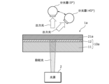
- FIG. 1 is a diagram showing the configuration of a phosphor device according to an embodiment.
- FIG. 2 is a diagram showing the configuration of the light source module according to the embodiment.
- FIG. 3 is a diagram showing the configuration of a phosphor device according to a comparative example.
- FIG. 4 is a diagram showing a table of constituent elements of the phosphor device according to the embodiment and the phosphor device according to the comparative example.
- FIG. 5 is a diagram showing the light emission characteristics of the phosphor device according to the embodiment and the phosphor device according to the comparative example.
- FIG. 6 is a cross-sectional view of the phosphor device according to Example 1.
- FIG. 1 is a diagram showing the configuration of a phosphor device according to an embodiment.
- FIG. 2 is a diagram showing the configuration of the light source module according to the embodiment.
- FIG. 3 is a diagram showing the configuration of a phosphor device according to a comparative example.
- FIG. 4 is a diagram showing
- FIG. 7 is a diagram showing the angular dependence of the chromaticity of the output light of the phosphor devices according to Study Examples 1 to 3.
- FIG. 8 is a diagram showing the angular dependence of the chromaticity of the output light of the phosphor devices according to Study Examples 4 to 6.
- FIG. 9 is a diagram showing the angular dependence of the chromaticity of the output light of the phosphor devices according to Examples 1 to 4 and Study Example 7.
- FIG. 10A is a diagram schematically showing the influence of Ce 3+ concentration and thickness on excitation light and fluorescence.
- FIG. 10B is a diagram showing the total luminous flux of the output light of nine types of samples each having a different thickness of the fluorescent part.
- FIG. 10C is a diagram showing the color temperature of nine types of samples each having a different thickness of the fluorescent part.
- FIG. 10D is a diagram showing the total luminous flux of output light of a plurality of four types of samples each having a different surface roughness of the fluorescent part.
- FIG. 11 is a diagram showing relative values of light reflectance of the first to third samples.
- FIG. 12 is a diagram showing an image showing the surface conditions of the first to third samples.
- FIG. 13 is a diagram showing luminescence images of three samples each having a different density of light reflecting portions.
- FIG. 14 is a diagram showing the area of the fluorescent part, the light-emitting area, and the value obtained by dividing the light-emitting area by the area of the fluorescent part of three samples having different densities of light-reflecting parts.
- FIG. 15 is a diagram showing an example of the light emission characteristics of three samples having different densities of light reflecting portions.
- FIG. 16 is a diagram showing another example of the light emission characteristics of three samples having different densities of light reflecting portions.
- FIG. 17 is a diagram showing relative values of light reflectance of the fourth to eighth samples.
- FIG. 18 is a diagram showing relative values of light reflectance of the 9th to 13th samples.
- FIG. 19 is a diagram showing the configuration of a phosphor device according to another example.
- each figure is a schematic diagram and is not necessarily strictly illustrated.
- symbol is attached to the substantially the same structure, and the overlapping description is omitted or simplified.
- the coefficient of linear expansion and the coefficient of linear expansion have the same meaning.
- the terms “upper” and “lower” do not refer to the upper direction (vertically upward) or the lower direction (vertically downward) in absolute spatial recognition, but are based on the stacking order in the stacked structure. Used as a term defined by the relative positional relationship. Additionally, the terms “above” and “below” are used not only when two components are spaced apart and there is another component between them; This also applies when two components are placed in close contact with each other.
- FIG. 1 is a diagram showing the configuration of a phosphor device 1 according to this embodiment.
- (a) is a top view of the phosphor device 1
- (b) is a cross-sectional view of the phosphor device 1 along line Ib-Ib in (a).
- the phosphor device 1 includes a substrate member 10 and a wavelength conversion member 20 provided on the substrate member 10.
- the substrate member 10 and the wavelength conversion member 20 are in direct thermal contact.
- the wavelength conversion member 20 is provided in direct contact with the upper surface of the substrate member 10. That is, there is no adhesive member such as an adhesive layer or a bonding member such as a bonding layer between the substrate member 10 and the wavelength conversion member 20.
- the surface of the contact surface of the substrate member 10 where the substrate member 10 contacts the wavelength conversion member 20 or the contact surface of the wavelength conversion member 20 where the wavelength conversion member 20 contacts the substrate member 10 is completely It may not be smooth.
- the substrate member 10 includes a light-transmitting base material 11, a dielectric multilayer film 12 and an antireflection film 13 provided on the light-transmitting base material 11. Further, the wavelength conversion member 20 includes a fluorescent portion 21 that emits fluorescence and a light reflecting portion 22 that reflects light.
- the light-transmitting base material 11 of the substrate member 10 is a substrate having light-transmitting properties, and has a first surface 11a (upper surface) that is a surface on the wavelength conversion member 20 side, and a second surface 11a that is opposite to the first surface 11a. It has a surface 11b (lower surface).
- the transparent base material 11 is preferably a substrate with high light transmittance.
- the light-transmitting base material 11 is preferably a transparent substrate with high transmittance to the extent that the other side can be seen through.
- the visible light transmittance of the transparent base material 11 is preferably 60% or more, more preferably 80% or more, and even more preferably 90% or more, but is not limited thereto.
- the light-transmitting base material 11 is preferably a substrate with high heat resistance.
- an alumina substrate made of Al 2 O 3 an aluminum nitride substrate made of AlN, or a gallium nitride substrate made of GaN can be used.
- the main components of the materials constituting the transparent base material 11 are Al 2 O 3 , AlN, or GaN, respectively.
- the transparent substrate having high heat resistance and light transmittance is not limited to these transparent substrates, and may be a transparent substrate such as a sapphire substrate or a glass substrate.
- the shape of the light-transmitting base material 11 is a rectangular thin plate having a length of 7.0 mm, a width of 7.0 mm, and a thickness of 1.0 mm.
- the dielectric multilayer film 12 is provided on the first surface 11a of the transparent base material 11.
- the dielectric multilayer film 12 is a surface film that is the uppermost layer of the substrate member 10.
- the dielectric multilayer film 12 has a structure in which a plurality of dielectric films are stacked, and reflects a specific light while transmitting other specific light.
- the dielectric multilayer film 12 in this embodiment reflects the light emitted by the fluorescent material of the fluorescent portion 21 of the wavelength conversion member 20 and transmits the excitation light incident on the fluorescent device 1 .
- the fluorescent section 21 is made of yellow phosphor and the excitation light that enters the phosphor device 1 is ultraviolet light or blue light
- the dielectric multilayer film 12 will reflect at least the yellow light emitted by the fluorescent section 21. , and transmits excitation light such as ultraviolet light or blue light.
- the dielectric multilayer film 12 By providing the dielectric multilayer film 12 on the first surface 11a side (wavelength conversion member 20 side) of the transparent base material 11 in this way, part of the light emitted by the fluorescent portion 21 of the wavelength conversion member 20 is absorbed into the substrate member 10.
- the dielectric multilayer film 12 can reflect the directed light. Thereby, it is possible to increase the amount of light from the fluorescent section 21 that can be taken out from the fluorescent device 1.
- the antireflection film 13 is provided on the second surface 11b of the transparent base material 11.
- the antireflection film 13 is a surface film that is the bottom layer of the substrate member 10.
- the antireflection film 13 may be either a single layer film or a multilayer film.
- the antireflection film 13 is made of silicon oxide (SiO 2 ), titanium oxide (TiO 2 ), niobium oxide (Nb 2 O 5 ), tantalum oxide (Ta 2 O 5 ), aluminum oxide (Al 2 O 3 ), It is a multilayer film in which at least two types of dielectric films such as aluminum nitride (AlN) are laminated.
- the anti-reflection film 13 By providing the anti-reflection film 13 on the second surface 11b of the transparent base material 11 in this way, light incident on the phosphor device 1 from the second surface 11b side of the transparent base material 11 is prevented from being reflected. Can be suppressed. Thereby, light that enters the light-transmitting base material 11 from the second surface 11b side of the light-transmitting base material 11 can be efficiently taken into the light-transmitting base material 11. Specifically, the excitation light that is incident on the phosphor device 1 to cause the fluorescent portion 21 to emit fluorescence can be efficiently introduced into the light-transmitting base material 11.
- the wavelength conversion member 20 is provided on the substrate member 10, and more specifically, provided above the substrate member 10.
- the fluorescent portion 21 of the wavelength conversion member 20 is a light emitting layer that emits light, and is excited by excitation light to emit fluorescent light of a predetermined wavelength in the visible light region.
- the fluorescent section 21 is a yellow phosphor layer made of yellow phosphor.
- the fluorescent section 21, which is a yellow phosphor layer emits fluorescence using light with a shorter wavelength than yellow light (for example, ultraviolet light to blue light) as excitation light. That is, in the yellow phosphor layer, the wavelength of the excitation light is converted into yellow light having a longer wavelength than the excitation light.
- the fluorescent portion 21 is a phosphor layer made only of phosphor.
- the fluorescent portion 21 is a phosphor ceramic layer made of a sintered single crystal phase phosphor, and the main component is the phosphor ceramic.
- the fluorescent section 21 is a yellow phosphor layer made of YAG (yttrium aluminum garnet) phosphor containing Ce 3+ . That is, the main component of the fluorescent part 21 is YAG phosphor ceramics containing Ce 3+ , and more specifically, the fluorescent part 21 is a member made only of YAG phosphor ceramics containing Ce 3+ . In other words, the fluorescent section 21 does not have a binder or the like.
- the Ce 3+ concentration of the YAG phosphor ceramic containing Ce 3+ that is the fluorescent part 21 is 0.005% or more and 0.02% or less.
- the fluorescent portion 21 is a phosphor ceramic layer consisting of only a single crystal phase.
- the fluorescent portion 21 includes a crystal phase having a garnet structure. More specifically, in this embodiment, the fluorescent portion 21 is composed only of a crystal phase having a garnet structure. That is, the fluorescent portion 21 according to the present embodiment does not include a crystal phase having a structure different from the garnet structure.
- the garnet structure is a crystal structure represented by the general formula A 3 B 2 C 3 O 12 .
- Rare earth elements such as Ca, Y, La, Ce, Pr, Nd, Sm, Eu, Gd, Tb and Lu are applied to element A, and rare earth elements such as Mg, Al, Si, Ga and Sc are applied to element B.
- Elements such as Al, Si, and Ga are applied to the element C.
- garnet structures include YAG, LuAG (lutetium aluminum garnet), Lu 3 Ga 2 (AlO 4 ) 3 (lutetium gallium aluminum garnet), Y 3 Ga 2 (AlO 4 ) 3 (yttrium Examples include gallium aluminum garnet), Lu 2 CaMg 2 Si 3 O 12 (lutetium calcium magnesium silicon garnet), and TAG (terbium aluminum garnet). These garnet structures are preferably used as the Ce 3+ activated phosphor.
- the material of the phosphor constituting the fluorescent portion 21 is (Y 1-x Cex ) 3 Al 2 Al 3 O 12 (that is, (Y 1-x Cex ) 3 Al 5 O 12 ) It is composed of a crystal phase expressed by (0.00005 ⁇ x ⁇ 0.0002), that is, YAG, and the fluorescent portion 21 is a fluorescent ceramic layer made only of sintered YAG.
- the fluorescent section 21 is a yellow phosphor layer made of YAG phosphor.
- the crystal phase constituting the fluorescent portion 21 may be a solid solution of a plurality of garnet crystal phases having different chemical compositions.
- a solid solution includes a garnet crystal phase represented by (Y 1-x Ce x ) 3 Al 2 Al 3 O 12 (0.00005 ⁇ x ⁇ 0.0002) and (Lu 1-d Ce d ) 3 Solid solution ( ( 1 -a)(Y 1 -x Ce x ) 3 Al 5 O 12 ⁇ a(Lu 1-d Ce d ) 3 Al 2 Al 3 O 12 (0 ⁇ a ⁇ 1)).
- such a solid solution includes a garnet crystal phase represented by (Y 1-x Ce x ) 3 Al 2 Al 3 O 12 (0.00005 ⁇ x ⁇ 0.0002) and (Lu 1-z Ce z ) 2 CaMg 2 Si 3 O 12 (0.00005 ⁇ z ⁇ 0.0002) Solid solution with garnet crystal phase ((1-b) (Y 1-x Ce x ) 3 Al 2 Al 3 O 12 ⁇ b(Lu 1-z Cez ) 2 CaMg 2 Si 3 O 12 (0 ⁇ b ⁇ 1)). Since the fluorescent part 21 is composed of a solid solution of a plurality of garnet crystal phases having different chemical compositions, the fluorescence spectrum of the fluorescence emitted by the fluorescent part 21 becomes broader, and the green light component and the red light component increase. Therefore, it is possible to provide a phosphor device 1 that emits output light with a wide color gamut.
- garnet crystal phase represented by (Y 1-x Ce x ) 3 Al 2 Al 3 O 12 (0.00005 ⁇ x ⁇ 0.0002) and (Lu 1-z Ce z )
- the crystal phase constituting the fluorescent portion 21 may include a crystal phase whose chemical composition is shifted from the crystal phase represented by the general formula A 3 B 2 C 3 O 12 described above.
- a crystal phase is an Al - rich ( Y 1 -x Ce x ) 3 Al 2+ ⁇ Al 3 O 12 ( ⁇ is a positive number).
- such a crystal phase is a Y-rich ( Examples include Y 1-x Ce x ) 3+ ⁇ Al 2 Al 3 O 12 ( ⁇ is a positive number).
- These crystal phases have different chemical compositions from the crystal phase represented by the general formula A 3 B 2 C 3 O 12 , but maintain the garnet structure. Since the fluorescent part 21 is composed of crystal phases with different chemical compositions, regions with different refractive indexes are created in the fluorescent part 21, so the excitation light and fluorescence are scattered more, and the light emitting area of the fluorescent part 21 is increased. becomes smaller.
- the following material which is a Cr 3+ activated fluorescent substance may be used.
- These materials include Y 3 Al 2 (AlO 4 ) 3 : Cr 3+ , La 3 Al 2 (AlO 4 ) 3 : Cr 3+ , Gd 3 Al 2 (AlO 4 ) 3 : Cr 3+ , Y 3 Ga 2 (AlO 4 ) 3 : Cr 3+ , La 3 Ga 2 (AlO 4 ) 3 : Cr 3+ , Gd 3 Ga 2 (AlO 4 ) 3 : Cr 3+ , Y 3 Sc 2 (AlO 4 ) 3 : Cr 3+ , La 3 Sc 2 (AlO 4 ) 3 : Cr 3+ , Gd 3 Sc 2 (AlO 4 ) 3 : Cr 3+ , Y 3 Ga 2 (GaO 4 ) 3 : Cr 3+ , La 3 Ga 2 (GaO 4 ) 3 : Cr 3+ , (Gd , La 3 Ga 2 (GaO 4
- the density of the fluorescent part 21 (that is, the density of the YAG phosphor ceramics) may be 90% or more and 100% or less of the theoretical density, preferably 95% or more and 100% or less of the theoretical density, and 98% of the theoretical density. It is even better if it is % or more and 100% or less.
- the theoretical density is the density assuming that the atoms in the layer are ideally arranged.
- the theoretical density is the density assuming that there are no voids in the fluorescent part 21, and is a value calculated using the crystal structure.
- the density of the fluorescent portion 21 is 99%, the remaining 1% corresponds to voids. In other words, the higher the density of the fluorescent portions 21, the fewer voids there are.
- the density of the fluorescent portions 21 is within the above range, the total amount of fluorescent light emitted by the fluorescent portions 21 increases, so it is possible to provide a phosphor device 1 that emits a larger amount of light.
- the density of the fluorescent portion 21 may be 4.10 g/cm 3 or more and 4.55 g/cm 3 or less, more preferably 4.32 g/cm 3 or more and 4.55 g/cm 3 or less, and 4. It is even better if it is 46 g/cm 3 or more and 4.55 g/cm 3 or less.
- the density of the fluorescent part 21 is 90% or more and 100% or less of the theoretical density, respectively. 95% or more and 100% or less and 98% or more and 100% or less.
- the excitation light absorbed by the fluorescent portion 21 can be efficiently converted into fluorescence. In other words, the fluorescent section 21 with high luminous efficiency is realized.
- the top view shape of the fluorescent section 21 is rectangular, but is not limited to this.
- the top view shape of the fluorescent portion 21 may be circular.
- the top view shape of the fluorescent section 21 is a rectangle measuring 0.8 mm in length and 0.8 mm in width.
- the thickness of the fluorescent portion 21 (that is, the thickness of the YAG phosphor ceramic) is 350 ⁇ m or more and 820 ⁇ m or less. This thickness is sufficiently thick, so that heat dissipation from the side surfaces of the fluorescent section 21 can be ensured. Note that the thickness of the fluorescent portion 21 is constant, but is not limited to this. Note that the thickness of the fluorescent portion 21 may be 350 ⁇ m or more and 805 ⁇ m or less, or 400 ⁇ m or more and 805 ⁇ m or less.
- the fluorescent section 21 has a light entrance surface 211, a light exit surface 212, and side surfaces (four side surfaces 213 to 216).
- the light incidence surface 211 is a surface onto which excitation light for exciting the fluorescent section 21 is incident, and is the lower surface of the fluorescent section 21 .
- the light emitting surface 212 is a surface from which the fluorescent section 21 emits fluorescent light, and is the upper surface of the fluorescent section 21 .
- the light entrance surface 211 and the light exit surface 212 are surfaces facing each other.
- the four side surfaces 213 to 216 are lateral surfaces of the fluorescent section 21. Each of the four side surfaces 213 to 216 is a plane perpendicular to the light entrance surface 211 and the light exit surface 212.
- the two side surfaces 213 and 215 are opposite surfaces, and the two side surfaces 214 and 216 are opposite surfaces.
- the light reflecting section 22 of the wavelength conversion member 20 is provided around the fluorescent section 21 when viewed from the direction of the light output surface 212, that is, when viewed from above.
- the light reflecting section 22 surrounds the entire periphery of the fluorescent section 21 when viewed from above.
- the light reflecting section 22 is in contact with all the four side surfaces 213 to 216 of the fluorescent section 21.
- the fluorescent section 21 has a rectangular shape when viewed from above
- the light reflecting section 22 has a rectangular opening.
- the shape of the light reflecting section 22 when viewed from above is a rectangular frame having a rectangular opening and a rectangular outer shape.
- the top view shape of the light reflecting section 22 is not limited to a rectangular frame shape, but may be an annular shape or the like.
- the outer shape of the light reflecting section 22 when viewed from above is 7.0 mm long x 7.0 mm wide.
- the thickness of the light reflection part 22 and the thickness of the fluorescent part 21 are the same, but are not limited to this.
- the light reflecting section 22 is in thermal contact with the fluorescent section 21. That is, the fluorescent section 21 and the light reflecting section 22 are provided so that the heat generated in the fluorescent section 21 can be conducted to the light reflecting section 22.
- the light reflecting section 22 is physically in contact with the fluorescent section 21. Specifically, the entire inner circumferential side surface of the light reflecting section 22 is in contact with the outer circumferential side surface of the fluorescent section 21 . That is, the fluorescent section 21 is provided so as to fill the opening of the light reflecting section 22.
- the thickness (height) of the light reflection section 22 is the same as the thickness (height) of the fluorescent section 21, it is not limited thereto. That is, the thickness of the light reflecting section 22 may be lower than the thickness of the fluorescent section 21 or may be higher than the thickness of the fluorescent section 21. However, it is preferable that the light reflecting section 22 be provided so as not to cover the upper surface of the fluorescent section 21 . That is, the light reflecting section 22 is preferably formed so that the material (such as a binder) constituting the light reflecting section 22 does not protrude onto the upper surface of the fluorescent section 21 .
- the main component of the light reflecting portion 22 is light reflective ceramics, and the main component of the light reflective ceramics is alumina ceramics. That is, here, the light reflecting portion 22 is constituted by a ceramic layer made of a ceramic material such as alumina (aluminum oxide (Al 2 O 3 )). More specifically, the light reflecting portion 22 is an alumina ceramic layer made only of alumina. In other words, the light reflecting section 22 does not include a binder or the like. In this embodiment, the light reflecting section 22 is white because it reflects light having a wavelength in the visible light band. In other words, the light reflecting section 22 is a white ceramic layer. Note that the light reflecting portion 22 does not need to be made of ceramics as long as it has the function of reflecting visible light. For example, the light reflecting portion 22 may be made of white resin or metal containing light reflective particles. It may be.
- the light reflecting section 22 that is, light reflecting ceramics
- the light reflecting section 22 is a ceramic layer
- the density of the light-reflecting portion 22 (that is, the density of the light-reflecting ceramic) may be 98% or less of the theoretical density, better if it is 95% or less, and even better if it is 90% or less.
- the fluorescent section 21 in this embodiment is a phosphor ceramic layer made of only sintered phosphor, and the light reflecting section 22 is a ceramic layer made of alumina ceramics. This facilitates integration of the fluorescent section 21 and the light reflecting section 22.
- FIG. 2 is a diagram showing the configuration of light source module 100 according to this embodiment.
- the light source module 100 includes a phosphor device 1 and a light source 2 that emits light that is incident on the phosphor device 1.
- the light source module 100 is used, for example, as a light emitting device included in an endoscope.
- the light source 2 is an excitation light source that emits excitation light for causing the fluorescent portion 21 of the wavelength conversion member 20 to emit light.
- the phosphor included in the fluorescent part 21 is excited by the excitation light emitted from the light source 2 and emits fluorescence.
- the light source module 100 is a transmission type light emitting device in which excitation light incident on the phosphor device 1 is transmitted through the phosphor device 1 . That is, the excitation light incident on the phosphor device 1 is transmitted through the wavelength conversion member 20. Therefore, the light source 2 is arranged such that the light emitted by the light source 2 is transmitted through the phosphor device 1. Specifically, the light source 2 is arranged below the phosphor device 1 (on the substrate member 10 side).
- the light source 2 for example, a semiconductor laser that emits ultraviolet or blue laser light can be used. Since laser light has excellent straightness, by using a semiconductor laser as the light source 2, the laser light (excitation light) can be made to enter the fluorescent section 21 at a desired angle of incidence.
- the light source 2 is not limited to a semiconductor laser, and may be another solid-state light emitting device such as an LED, or an excitation light source other than a solid-state light emitting device.
- the light source module 100 configured in this way, when the light emitted from the light source 2 enters the phosphor device 1, output light of a predetermined color is emitted from the phosphor device 1. More specifically, output light of a predetermined color is emitted from the light exit surface 212 of the fluorescent section 21 .
- the light (excitation light) emitted from the light source 2 is incident on the back surface of the substrate member 10.
- the light (excitation light) from the light source 2 that has entered the substrate member 10 passes through the substrate member 10 and reaches the fluorescent portion 21 of the wavelength conversion member 20 . That is, the excitation light emitted from the light source 2 enters the fluorescent section 21 from the light incident surface 211 of the fluorescent section 21.
- the external size of the fluorescent section 21 is preferably equal to the spot size (spot size of excitation light) when the light emitted from the light source 2 enters the fluorescent section 21 .
- the excitation light of the light source 2 is blue light
- the fluorescent section 21 is a yellow phosphor layer.
- the blue light from the light source 2 enters the fluorescent section 21 .
- the yellow phosphor (YAG phosphor) of the fluorescent section 21 absorbs a portion of the blue light from the light source 2, is excited, and emits yellow light as fluorescence.
- this yellow light and the blue light from the light source 2 that is not absorbed by the yellow phosphor are mixed to become white light, and this white light is emitted from the fluorescent section 21 as output light. That is, output light (white light) is extracted from the wavelength conversion member 20.
- a dielectric multilayer film 12 is formed on the substrate member 10.
- the dielectric multilayer film 12 reflects yellow light emitted by the fluorescent section 21 and transmits blue light, which is excitation light. With this configuration, of the yellow light emitted by the fluorescent section 21, the light directed toward the light source 2 is reflected by the dielectric multilayer film 12 and travels toward the opposite side from the light source 2.
- a white light reflecting section 22 is formed around the fluorescent section 21.
- the output light (white light) emitted from the fluorescent section 21 the light traveling in the horizontal direction is reflected by the light reflecting section 22, returns to the fluorescent section 21, and is emitted from the fluorescent section 21 to the outside. be done. Thereby, it is possible to increase the amount of light that can be extracted from the fluorescent section 21.
- the phosphor device 1 is of a remote phosphor type, and the phosphor device 1 and the light source 2 are arranged spatially apart. Thereby, it is possible to suppress the influence of the heat generated by the light source 2 on the phosphor device 1 (especially the phosphor section 21).
- the light emitted from the light source 2 is incident perpendicularly to the back surface of the substrate member 10, but it may be incident obliquely to the back surface of the substrate member 10.
- a light guide (not shown) is provided above the phosphor device 1, and the output light incident on this light guide is used for the endoscope. Used as light. The more light that is incident on the light guide among the output light output from the phosphor device 1, the higher the utilization efficiency of the output light.
- the light guide is an optical member composed of a lens, a rod integrator, and the like.
- the light source module 100 is a white light source module.
- FIG. 3 is a diagram showing the configuration of a phosphor device 1x according to a comparative example.
- the phosphor device 1x includes a substrate member 10 and a wavelength conversion member 20x arranged above the substrate member 10. Further, the wavelength conversion member 20x includes a fluorescent portion 25x and a binder 26x.
- FIG. 4 is a diagram showing a table of constituent elements of the phosphor device 1 according to the present embodiment and the phosphor device 1x according to the comparative example.
- the wavelength conversion member 20x included in the phosphor device 1x according to the comparative example does not have the light reflection section 22, unlike the wavelength conversion member 20 according to the embodiment. Furthermore, the density of the light reflecting portions 22 included in the wavelength conversion member 20 according to the embodiment is 81.1% of the theoretical density, as shown in FIG.
- the light emitting area is approximately 0.34 mm 2 in the comparative example, and approximately 0.64 mm 2 (0.8 mm ⁇ 0.8 mm) in the embodiment.
- the fluorescent portion 25x is a fluorescent particle, more specifically, a fluorescent particle made of YAG.
- the binder 26x is a material for holding the fluorescent portion 25x and adhering it above the substrate member 10, and is, for example, transparent ZnO crystal.
- the refractive index of the wavelength conversion member 20x consisting of the fluorescent portion 25x and the binder 26x is approximately 1.95, and the refractive index of the fluorescent portion 21 is 1.83.
- the Ce 3+ concentration in YAG constituting the fluorescent section 25x according to the comparative example is about 0.1%, and the Ce 3+ concentration in YAG constituting the fluorescent section 21 according to the embodiment is 0.01%.
- the thickness of the wavelength conversion member 20x according to the comparative example is about 20 ⁇ m, and the thickness of the fluorescent section 21 according to the embodiment is 500 ⁇ m or more and 700 ⁇ m or less. Further, the density of the fluorescent portion 21 is 98.8% of the theoretical density.
- the luminance distribution when the excitation light is irradiated is shown as a gradation.
- the entire fluorescent section 21 that is, the entire 0.64 mm 2 of 0.8 mm x 0.8 mm
- FIG. 5 is a diagram showing the light emission characteristics of the phosphor device 1 according to the present embodiment and the phosphor device 1x according to the comparative example.
- the horizontal axis in FIG. 5 indicates the power input to emit excitation light from the light source 2 (input power).
- the vertical axis in FIG. 5 indicates the total luminous flux of light that enters the light guide provided above the phosphor device 1 and the phosphor device 1x and exits from the light guide.
- the light emitted from this light guide may be described as light guide light.
- the total luminous flux of the light guide light based on the output light output from the phosphor device 1 is the total luminous flux of the light guide light based on the output light output from the phosphor device 1x. higher than the luminous flux.
- the total luminous flux of the light guide light based on the output light output from the phosphor device 1 is the total luminous flux of the light guide light based on the output light output from the phosphor device 1x. It's about 30% higher than that.
- the total luminous flux of the light guide light based on the output light output from the phosphor device 1 is equal to the total luminous flux of the light guide light based on the output light output from the phosphor device 1x. It is about 46% higher than the total luminous flux.
- the factors why the phosphor device 1 according to the present embodiment has higher light emission characteristics than the phosphor device 1x according to the comparative example will be described below.
- the phosphor device 1 is provided with a light reflecting section 22. Therefore, among the output light (white light) emitted from the fluorescent section 21, the light traveling in the horizontal direction is reflected by the light reflecting section 22, returns to the fluorescent section 21, and is emitted from the fluorescent section 21 to the outside. Ru. That is, out of the output light (white light) emitted from the fluorescent section 21, the light that travels in the horizontal direction is suppressed from becoming unusable light. Therefore, the total luminous flux of the light guide light based on the output light output from the phosphor device 1 becomes higher.
- a phosphor ceramic layer is used as the phosphor portion 21. Therefore, the heat resistance and heat dissipation of the fluorescent section 21 can be improved, and the luminous efficiency of the fluorescent section 21 is less likely to decrease due to heat. In particular, if the density of the fluorescent portion 21 (that is, the density of the YAG phosphor ceramic) is within the above range, the luminous efficiency of the fluorescent portion 21 is less likely to decrease due to heat. Further, by using a phosphor ceramic layer as the fluorescent part 21, it is possible to suppress light loss due to scattering of fluorescence, and thus the conversion efficiency of the fluorescent part 21 can be improved. Therefore, the total luminous flux of the light guide light based on the output light output from the phosphor device 1 becomes higher.
- the phosphor device 1 according to the present embodiment has higher light emission characteristics than the phosphor device 1x according to the comparative example.
- FIG. 6 is a cross-sectional view of the phosphor device 1a according to Example 1.
- the phosphor device 1a includes a substrate member 10a and a phosphor section 21a.
- the substrate member 10a has a structure in which the antireflection film 13 is removed from the substrate member 10, and in other words, it has a transparent base material 11 and a dielectric multilayer film 12 provided on the transparent base material 11. are doing.
- the fluorescent part 21a included in the phosphor device 1a is a fluorescent part 21a, except that it is provided in contact with the upper part of the dielectric multilayer film 12 and that no light reflecting part 22 is provided around it. It has the same configuration as the fluorescent section 21 included in the device 1.
- the Ce 3+ concentration is 0.01% and the thickness is 705 ⁇ m.
- each of the phosphor devices according to Study Examples 1 to 7 and Examples 2 to 4 has the same configuration as the phosphor device 1a except for the Ce 3+ concentration and thickness of the fluorescent portion. More specifically, the Ce 3+ concentration and thickness of the fluorescent part are 0.08% and 225 ⁇ m in Study Example 1, 0.08% and 125 ⁇ m in Study Example 2, and 0.08% and 57 ⁇ m in Study Example 3, respectively. It is. Further, the Ce 3+ concentration and thickness of the fluorescent part are 0.03% and 666 ⁇ m in Study Example 4, 0.03% and 400 ⁇ m in Study Example 5, and 0.03% and 300 ⁇ m in Study Example 6, respectively. In addition, the Ce 3+ concentration and thickness of the fluorescent part are 0.01% and 659 ⁇ m in Example 2, 0.01% and 400 ⁇ m in Example 3, 0.01% and 805 ⁇ m in Example 4, and Study Example 7. 0.01% and 300 ⁇ m.
- the phosphor devices according to Examples 1 to 4 correspond to the phosphor device 1 according to the present embodiment in terms of Ce 3+ concentration and thickness.
- Table 1 shows the target composition, raw materials used, and raw material blending ratio of the phosphor parts (YAG phosphor ceramics) used in the phosphor devices according to Study Examples 1 to 7 and Examples 1 to 4. This is a table.
- each raw material shown in Table 1 was placed in a plastic pot (hereinafter referred to as pot) with a volume of 1 L. At this time, each raw material used and an alumina ball ( ⁇ 10 mm) were put into the pot. The amount of alumina balls was set to fill approximately 1/3 of the volume of the pot.
- Ball mill mixing was performed for 12 hours using a pot rotating device (BALL MILL ANZ-51S, manufactured by Nichito Kagaku Co., Ltd.).
- the slurry-like mixed raw materials were dried using a dryer after ball mill mixing. Specifically, the above mixed raw material was poured onto a Naflon (registered trademark) sheet (thickness: 0.05 mm) spread over the inner wall of a metal bat, and the mixed raw material was placed in a dryer set at 150°C. for 6 hours to dry.
- a Naflon (registered trademark) sheet thinness: 0.05 mm
- the dried mixed raw materials were collected and granulated using a mortar and pestle. Specifically, the mixed raw material after drying was put into a mortar and ground to obtain a mixed raw material powder. Furthermore, 0.18 mL of a binder liquid (5 wt.% PVA (polyvinyl alcohol) solution) was added little by little to 10 g of mixed raw material powder using a pipette, and kneaded using a pestle. In other words, the binder liquid was dispersed throughout the mixed raw material powder. Thereafter, the mixed raw material powder was classified using a nylon mesh to obtain granulated powder. Note that the opening diameter of the nylon mesh was 155 ⁇ m. In this way, raw materials for powdered fluorescent parts (YAG phosphor ceramics) for Study Examples 1 to 7 and Examples 1 to 3 were obtained.
- a binder liquid 5 wt.% PVA (polyvinyl alcohol) solution
- Example 4 after ball mill mixing, the slurry-like mixed raw materials were granulated using a spray dryer device. More specifically, 0.5wt. % of a binder (for example, PVA (polyvinyl alcohol)) was added to the slurry-like mixed raw material, which was granulated using a spray dryer device. The average particle diameter of the obtained granulated powder was 45 ⁇ m. In this way, a raw material for the powdered fluorescent part (YAG fluorescent ceramics) for Example 4 was obtained.
- a binder for example, PVA (polyvinyl alcohol)
- each raw material was molded into a cylindrical shape using a manual hydraulic press machine (manufactured by Riken Seiki Co., Ltd.) and a mold ( ⁇ 13 mm).
- the pressure applied to the sample during mold molding was 6 MPa.
- the raw material was actually molded using a cold isostatic press (CIP) device.
- the pressure during main molding was 250 MPa.
- the molded body after this molding was subjected to binder removal treatment (heat treatment in the air) for the purpose of removing the adhesive (polyvinyl alcohol) used during granulation.
- the conditions for the binder removal treatment were 500° C. and 10 hours.
- Example 4 The raw material for Example 4 was molded in the same manner as the raw materials for Study Examples 1 to 7 and Examples 1 to 3, except for one point below.
- the one point is that a mold ( ⁇ 60 mm) was used when a manual hydraulic press machine (manufactured by Riken Seiki Co., Ltd.) was used.
- each molded body was fired using a vertical tubular atmosphere furnace.
- the firing temperature was 1725°C.
- the firing time was 4 hours.
- the firing atmosphere was 97vol. % nitrogen and 3 vol. % hydrogen as a mixed gas. Further, the flow rate of the mixed gas was 1 L/min.
- Example 4 firing in Example 4 will be explained.
- the raw material for Example 4 after the binder removal treatment was fired using a vertical tubular atmosphere furnace under the following conditions.
- the conditions are that the firing temperature is 1700°C or more and 1725°C or less, the firing time is 4 hours or more and 24 hours or less, and the firing atmosphere is 95 vol. % or more 97vol. % nitrogen and 3 vol. % or more 5vol. % or less of hydrogen, and the flow rate of the mixed gas is 1 L/min or more and 5 L/min or less.
- each sample was mirror-polished using a polishing device (DFD6340, manufactured by DISCO Co., Ltd.).
- the thickness after mirror polishing was set to three levels: 225 ⁇ m (examination example 1), 125 ⁇ m (examination example 2), and 57 ⁇ m (examination example 3) for samples with a Ce 3+ concentration of 0.08%.
- Samples with a Ce 3+ concentration of 0.03% had three levels: 666 ⁇ m (Study Example 4), 400 ⁇ m (Study Example 5), and 300 ⁇ m (Study Example 6).
- the samples with a Ce 3+ concentration of 0.01% were 705 ⁇ m (Example 1), 659 ⁇ m (Example 2), 400 ⁇ m (Example 3), 805 ⁇ m (Example 4), and 300 ⁇ m (Study Example 7). It was set as 4 levels.
- each sample was diced using a dicing device (DAD3350, manufactured by Disco Corporation).
- DAD3350 manufactured by Disco Corporation.
- the samples of Study Examples 1 to 7 and Examples 1 to 3 were diced into squares with sides of 7 mm, and the samples of Example 4 were diced into squares with sides of 10 mm.
- fluorescent parts according to Study Examples 1 to 7 and Examples 1 to 4 were manufactured.
- the density of each fluorescent part was evaluated using the Archimedes method. Then, assuming the theoretical density of YAG to be 4.55 g/cm 3 , the ratio of each fluorescent part to the theoretical density was calculated.
- the chromaticity of the output light in the direction was measured by a spectrometer. Note that the output light output in the 0° direction and the 45° direction corresponds to the light that enters the above-mentioned light guide. More specifically, the chromaticity of the output light was measured as follows.
- each sample after dicing was placed above the substrate member 10a, and phosphor devices according to Study Examples 1 to 7 and Examples 1 to 4 were fabricated.
- Each of the phosphor devices according to Study Examples 1 to 7 and Examples 1 to 4 is irradiated with a 0.83 W laser beam from the light source 2 from the substrate member 10a side.
- the laser beam irradiation spot area was 4 mm 2 .
- the transparent base material 11 is a sapphire substrate, and has a rectangular shape of 7 mm x 7 mm for the samples of Study Examples 1 to 7 and Examples 1 to 3, and
- the sample has a rectangular shape of 10 mm x 10 mm and a thickness of 500 ⁇ m.
- the dielectric multilayer film 12 is a film that transmits blue light and reflects light in a wavelength range of 480 nm or more and 780 nm or less with a reflectance of 90% or more.
- the angular dependence of the chromaticity of the output light output from each of the phosphor devices according to Study Examples 1 to 7 and Examples 1 to 4 was measured by irradiation with laser light.
- Each of the output lights was measured using an integrating sphere (manufactured by Nemtech Co., Ltd.) and a multichannel spectrometer (manufactured by Otsuka Electronics Co., Ltd., MCPD-7000). Note that here, each phosphor device is not provided with a light reflecting section. However, the chromaticity of the output light and the angular dependence of the chromaticity of the output light are presumed to be the same as in the case where a light reflecting section is provided.
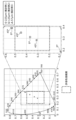
- FIG. 7 is a diagram showing the angular dependence of the chromaticity of the output light of the phosphor devices according to Study Examples 1 to 3.
- FIG. 8 is a diagram showing the angular dependence of the chromaticity of the output light of the phosphor devices according to Study Examples 4 to 6.
- FIG. 9 is a diagram showing the angular dependence of the chromaticity of the output light of the phosphor devices according to Examples 1 to 4 and Study Example 7.
- FIGS. 7 to 9 xy chromaticity diagrams are shown in FIGS. 7 to 9, and the chromaticity of output light of each phosphor device in the 0° direction and 45° direction is shown in the xy chromaticity diagram.
- FIGS. 7 to 9 a rectangular chain line showing a part of the xy chromaticity diagram is shown enlarged.
- FIGS. 7 to 9 a rectangular broken line is shown, and this broken line indicates the permissible chromaticity range when a light source module including a phosphor device is used in an endoscope, for example. .
- the light source module is used for an endoscope, both the output light in the 0° direction and the output light in the 45° direction are used as light for the endoscope. Therefore, if both the chromaticity in the 0° direction and the chromaticity in the 45° direction fall within this chromaticity range (rectangular broken line), it is determined that the light source module can be used as a light emitting device for an endoscope. be done.
- a light source module including a phosphor device with a small angular dependence of chromaticity of output light has higher performance as a light emitting device for an endoscope.
- Table 2 is a table showing the xy coordinates of the chromaticity of the output light of the phosphor devices according to Study Examples 1 to 3.
- Table 3 is a table showing the xy coordinates of the chromaticity of the output light of the phosphor devices according to Study Examples 4 to 6.
- Table 4 is a table showing the xy coordinates of the chromaticity of the output light of the phosphor devices according to Examples 1 to 4 and Study Example 7.
- the chromaticity in the 0° direction and the chromaticity in the 45° direction are within the chromaticity range (rectangular broken line); It is clear that the difference with the chromaticity in the ° direction is very large. On the other hand, in all of the phosphor devices according to Examples 1 to 4, the difference between the chromaticity in the 0° direction and the chromaticity in the 45° direction is very small, which means that the angular dependence of chromaticity is is shown to be small.
- the phosphor device according to Examination Example 6 see FIG. 8
- the phosphor device according to Example 2 see FIG. 9
- the angular dependence of chromaticity in the phosphor device according to Example 2 is smaller than the angular dependence of chromaticity in the phosphor device according to Study Example 6.
- the phosphor device according to Example 2 in which the Ce 3+ concentration in the fluorescent portion is sufficiently low, has been shown to have smaller angular dependence of chromaticity.
- the Ce 3+ concentration is 0.01% and the thickness is 350 ⁇ m or more and 820 ⁇ m or less, so that the chromaticity of the output light is lower than in Examples 1 to 7.
- a phosphor device with small angular dependence has been realized. This principle will be explained using FIG. 10A.
- FIG. 10A is a diagram schematically showing the influence of Ce 3+ concentration and thickness on excitation light and fluorescence.
- FIG. 10A a fluorescent part with a changed Ce 3+ concentration and thickness, and excitation light (blue light) and fluorescence (yellow light) reaching the fluorescent part are schematically shown.
- the ratio of the lengths of the solid line arrow indicating blue light and the broken line arrow indicating yellow light indicates the ratio of the blue light intensity and yellow light intensity in the output light.
- the fluorescent portion having a high Ce 3+ concentration and a thick thickness corresponds to Study Example 4, and the fluorescent portion having a high Ce 3+ concentration and a thin thickness corresponds to Study Example 6. Further, the fluorescent portion having a low Ce 3+ concentration and a thick thickness corresponds to Example 2, and the fluorescent portion having a low Ce 3+ concentration and a thin thickness corresponds to Study Example 7.
- Example 2 the intensity of the yellow light is lower in the 0° direction and the 45° direction than in Examination Example 6, so the output light becomes light close to white. Further, since the difference in the ratio of the length of the solid line arrow (blue light) to the length of the broken line arrow (yellow light) is small between the 0° direction and the 45° direction, the angular dependence of chromaticity is small.
- the phosphor devices according to Examples 1 to 4 correspond to the phosphor device 1 according to the present embodiment in terms of Ce 3+ concentration and thickness. Therefore, like the phosphor devices according to Examples 1 to 4, the phosphor device 1 according to the present embodiment has chromaticity in the 0° direction and 45° direction within the chromaticity range, and This results in a phosphor device with small angular dependence.
- the thickness of the fluorescent part 21 of the six types of samples is 350 ⁇ m or more and 820 ⁇ m or less.
- the designed thicknesses of the fluorescent portions 21 in the six types of samples are 575 ⁇ m, 641 ⁇ m, 680 ⁇ m, 747 ⁇ m, 753 ⁇ m, and 802 ⁇ m, respectively.
- a sample with a designed thickness of the fluorescent part 21 is 575 ⁇ m
- a sample with a design thickness of 641 ⁇ m is a sample of 641 ⁇ m
- a sample with a design thickness of 680 ⁇ m is a sample of 680 ⁇ m
- a sample with a design thickness of 747 ⁇ m is a sample of 747 ⁇ m
- a sample with a design thickness of 753 ⁇ m is a sample of 753 ⁇ m.
- a sample having a diameter of 802 ⁇ m may be described as sample 802 ⁇ m.
- the remaining three types of samples among the nine types of samples have the same configuration as the phosphor device 1 shown in FIG. 1 except that the thickness of the fluorescent part is different.
- the thickness of the section is greater than 820 ⁇ m.
- the designed thicknesses of the fluorescent parts in the three types of samples are 826 ⁇ m, 873 ⁇ m, and 918 ⁇ m.
- a sample with a designed thickness of the fluorescent portion of 826 ⁇ m may be referred to as a sample 826 ⁇ m, a sample with a design thickness of 873 ⁇ m as a sample 873 ⁇ m, and a sample with a design thickness of 918 ⁇ m as a sample 918 ⁇ m.
- YAG phosphor ceramics were produced to be used in the fluorescent parts of each of the nine types of samples.
- the target composition of the YAG phosphor ceramic used in the fluorescent part was the same as that of the YAG phosphor ceramic used in the phosphor devices of Examples 1 to 4 and Study Example 7. Further, the YAG phosphor ceramic used in the phosphor section was manufactured by the same method as the YAG phosphor ceramic used in the phosphor device of Example 4 up to the step of firing (firing step).
- the YAG phosphor ceramics that have been subjected to the firing process are then processed using a polishing device (manufactured by DISCO Co., Ltd., DFD6340) and a dicing device (manufactured by DISCO Co., Ltd., DAD3350) to a size of 0.8 mm in length and 0.8 mm in width.
- the shape was processed so that the height was 0.8 mm and the height was 1 mm or more.
- a mold ( ⁇ 13 mm) was prepared, and Al 2 O 3 powder having an average primary particle diameter of 0.28 ⁇ m was charged into the mold.
- the shaped YAG phosphor ceramics were then placed into the Al 2 O 3 powder that filled the mold.
- the shaped YAG phosphor ceramic was placed near the center of the Al 2 O 3 powder filling the mold so that its height direction was substantially perpendicular to the ground. Then, using a manual hydraulic press machine (manufactured by Riken Seiki Co., Ltd.), it was molded into a substantially cylindrical shape. The pressure applied to the sample during mold molding was 6 MPa. Next, main molding was performed using a cold isostatic press (CIP) device. The pressure during main molding was 250 MPa. In this way, a composite molded body was produced in which the shaped YAG phosphor ceramic was placed in Al 2 O 3 powder. The produced composite molded body was fired using a box-type atmospheric furnace. The firing temperature was 1200°C to 1300°C.
- the firing time was 2 hours.
- a composite ceramic consisting of shaped YAG phosphor ceramics and Al 2 O 3 ceramics was produced.
- the produced composite ceramics were changed into nine different thicknesses using a polishing device (DFD6340, manufactured by DISCO Co., Ltd.).
- DMD6340 manufactured by DISCO Co., Ltd.
- Each of the nine types of composite ceramics with different thicknesses was diced using a dicing device (DAD3350, manufactured by DISCO Co., Ltd.) to a length of 7.0 mm so that the YAG phosphor ceramic was placed approximately in the center. It was shaped into a square with a width of 7.0 mm.
- sample 575 ⁇ m, sample 641 ⁇ m, sample 680 ⁇ m, sample 747 ⁇ m, sample 753 ⁇ m, and sample 802 ⁇ m are phosphor devices having the same configuration as phosphor device 1 shown in FIG. It is.
- These nine types of samples are samples in which the thickness of the fluorescent portion (thickness in the vertical direction in FIG. 1) has been changed. The total luminous flux of output light output from each of the nine types of samples was measured.
- FIG. 10B is a diagram showing the total luminous flux of the output light of nine types of samples each having a different thickness of the fluorescent part.
- the total luminous flux of the output light of each of the nine types of samples is measured when the power input to emit the excitation light is 5.2 W.
- Table 5 is a table showing the thickness of the fluorescent part and the total luminous flux of output light of nine types of samples.
- the total luminous flux of the output light output from the nine types of samples is all 930 lm or more, and more specifically, 1200 lm or more. Furthermore, it has been shown that the thicker the fluorescent part is, the higher the total luminous flux tends to be.
- the total luminous flux of the output light output from the phosphor device 1 should be 930 lm or more. is required.
- Six types of samples that is, sample 575 ⁇ m, sample 641 ⁇ m, sample 680 ⁇ m, sample 747 ⁇ m, sample 753 ⁇ m, and sample 802 ⁇ m) in which the thickness of the fluorescent portion 21 is 350 ⁇ m or more and 820 ⁇ m or less are the fluorescence according to the present embodiment as described above.
- the samples correspond to the body device 1, and the total luminous flux of the output light of the six types of samples is all 930 lm or more.
- the phosphor device 1 (each of the six types of samples) is a device with a high total luminous flux of output light to the extent that it can be used in an endoscope.
- the three types of samples in which the thickness of the fluorescent part is larger than 820 ⁇ m are also samples with a high total luminous flux of output light to the extent that they can be used in an endoscope from the viewpoint of total luminous flux.
- the phosphor device 1 is a fluorescent material whose chromaticity in the 0° direction and the 45° direction falls within the chromaticity range, and whose angular dependence of chromaticity is small. It is shown that it is a body device. Therefore, in this embodiment, the Ce 3+ concentration is 0.01% and the thickness is 350 ⁇ m or more and 820 ⁇ m or less, so that the angular dependence of the chromaticity of the output light is small and the total luminous flux of the output light is A high quality phosphor device 1 has been realized.
- FIG. 10C is a diagram showing the color temperature of nine types of samples each having a different thickness of the fluorescent part. Further, in FIG. 10C, an approximate straight line calculated by the least squares method based on the color temperatures of nine types of samples is shown as a dashed-dotted line.
- Table 6 is a table showing the thickness of the fluorescent part and the color temperature of the output light of nine types of samples.
- the color temperature of the output light output from the phosphor device 1 is 3500K or more and 15000K or less.
- a range of 4500K or more and 7000K or less is better, and a range of 5050K or more and 5810K or less is even more suitable.
- Three types of samples that is, sample 747 ⁇ m, sample 753 ⁇ m, and sample 802 ⁇ m) in which the thickness of the fluorescent portion 21 is 747 ⁇ m or more and 802 ⁇ m or less are samples corresponding to the phosphor device 1 according to the present embodiment as described above. .
- the color temperatures of the output light of the three types of samples are all 5050K or more and 5810K or less, that is, the values are within the above-mentioned more suitable range. Further, when calculated using the approximate straight line in FIG. 10C, it is estimated that if the sample has a fluorescent portion with a thickness in the range of 726 ⁇ m or more and 902 ⁇ m or less, the color temperature will be a value within the above-mentioned more suitable range. Note that, as explained in FIG. 10A and the like, the color temperature changes due to a change in the thickness of the fluorescent part.
- the thickness of the phosphor portion 21 is 726 ⁇ m or more and 820 ⁇ m or less, the color temperature of the output light is in a more suitable range. , and the angular dependence of the chromaticity of the output light is small, as shown in FIG. Therefore, the phosphor device 1 according to this embodiment can be more easily used in endoscopes.
- the thickness of the fluorescent portion 21 is not limited to the above, and may be 750 ⁇ m or more and 820 ⁇ m or less, 770 ⁇ m or more and 820 ⁇ m or less, or 790 ⁇ m or more and 820 ⁇ m or less.
- YAG phosphor ceramics to be used for the fluorescent portions 21 of each of the four types of samples were manufactured.
- the target composition of the YAG phosphor ceramic used in the phosphor section 21 was the same as that of the YAG phosphor ceramic used in the phosphor devices of Examples 1 to 4 and Study Example 7.
- the YAG phosphor ceramic used in the phosphor section 21 is different from the YAG phosphor ceramic used in the phosphor devices of Examples 1 to 3 and Study Example 7 until the firing step (firing step). Made using the same method.
- FIG. 10D is a diagram showing the total luminous flux of output light of four types of samples whose fluorescent parts 21 have different surface roughnesses.
- the total luminous flux of the output light of each of the four types of samples is measured when the power input to emit the excitation light is 5.2 W.
- sample (1400/8000) A sample (hereinafter referred to as sample (1400/8000)) was prepared in which the light exit surface 212 was polished with a grindstone grain size of No. 1400 and the light incidence surface 211 was polished with a grindstone grain size of No. 8000.
- sample (600/600) A sample (hereinafter referred to as sample (600/600)) was prepared in which the light exit surface 212 was polished with a grindstone grain size of No. 600 and the light incidence surface 211 was polished with a grindstone grain size of No. 600.
- sample (1400/1400) was prepared in which the light exit surface 212 was polished with a grindstone grain size of No.
- sample 4000/4000 A sample (hereinafter referred to as sample (4000/4000)) was prepared in which the light exit surface 212 was polished with a grindstone grain size of No. 4000, and the light incidence surface 211 was polished with a grindstone grain size of No. 4000.
- the horizontal axis in FIG. 10D indicates the grindstone grain size used to polish the light exit surface 212 of each of the four types of samples. Further, FIG. 10D shows the correlation between the grindstone grain size and the surface roughness (more specifically, the arithmetic mean roughness Ra). That is, the Ra of each of the light exit surface 212 and the light entrance surface 211 of the sample (600/600) is 145 nm. The Ra of each of the light exit surface 212 and the light entrance surface 211 of the sample (1400/1400) is 137 nm. Ra of the light exit surface 212 of the sample (1400/8000) is 137 nm. Note that the Ra of the light incident surface 211 of the sample (1400/8000) is 11 nm. Ra of each of the light exit surface 212 and the light entrance surface 211 of the sample (4000/4000) is 20 nm.
- the sample (1400/8000) is a reference sample and has a sufficiently high total luminous flux. It is preferable that a total luminous flux equivalent to that of the sample (1400/8000) be obtained for other samples as well.
- the average value of the total luminous flux of 2 samples (600/600), the average value of the total luminous flux of 2 samples (1400/1400), and the average value of the total luminous flux of 3 samples (4000/4000) are Each is equivalent to the average value of the total luminous flux of two samples (1400/8000).
- the number of man-hours or cost for manufacturing a sample in which the light incidence surface 211 has an Ra of 20 nm or more is reduced.
- Al 2 O 3 powder having an average particle diameter of 0.2 ⁇ m and an ⁇ -type crystal system was used as a raw material for each sample.
- This Al 2 O 3 powder was molded into a cylindrical shape using a manual hydraulic press machine (manufactured by Riken Seiki Co., Ltd.) and a mold ( ⁇ 13 mm). The pressure applied to each sample when molding the Al 2 O 3 powder was 6 MPa. Next, each of the mold-molded samples was subjected to actual molding using a cold isostatic pressurizing device. The pressure applied to each sample during main molding was 250 MPa. Note that no binder was used when molding and main molding were performed. In this way, a molded body of the raw material for the light reflecting section 22 was obtained.
- the molded body was fired using an atmospheric electric furnace.
- the firing temperature was in the range of about 1100° C. or more and about 1500° C. or less, and three samples with different densities were produced by changing the firing temperature.
- the respective densities of the three samples were 3.230 g/cm 3 , 3.788 g/cm 3 , and 3.950 g/cm 3 . Further, the ratios of the three samples to the respective theoretical densities were 81.1%, 95.0%, and 100%.
- a sample with a density of 3.230 g/cm 3 is used as a first sample
- a sample with a density of 3.950 g/cm 3 May be stated. Note that the higher the firing temperature, the higher the density of the sample, that is, the higher the ratio of the sample to the theoretical density.
- the density of the light reflecting portion 22 (that is, the density of the light reflecting ceramic) according to the present embodiment only needs to be 98% or less of the theoretical density, so that the first sample and the second sample are This corresponds to the light reflecting section 22.
- the main component of the light reflecting section 22 is light reflective ceramics, the main components of the first and second samples corresponding to the light reflecting section 22 are also light reflecting ceramics.
- the light reflectivity in the visible light region was measured for three samples related to the light reflecting section 22.
- FIG. 11 is a diagram showing the relative values of the light reflectance of the first to third samples. Note that FIG. 11 shows first and second samples that correspond to the light reflection section 22 and a third sample that does not correspond to the light reflection section 22.
- the relative value of light reflectance is measured as follows.
- the visible light reflectance (relative value of light reflectance) of each sample was evaluated using a spectrofluorometer (JASCO Corporation, FP-6500).
- the ratio of the reflection intensity of light in the wavelength range of 400 nm to 800 nm of each sample to the reflection intensity of light in the wavelength range of 400 nm to 800 nm of the plate-shaped barium sulfate member is the relative value of light reflectance. It was measured as. That is, the relative value of light reflectance means relative reflectance.
- the light traveling in the horizontal direction is reflected by the light reflecting section 22, and The light returns to the fluorescent section 21 and is emitted from the fluorescent section 21 to the outside. Therefore, the higher the relative value of the light reflectance of the light reflection section 22, the more the output light output from the phosphor device 1 increases.
- the density of the sample corresponding to the light reflecting portion 22 may be 98% or less of the theoretical density, preferably 95% or less, and 90% or less of the theoretical density. It is even better if it is less than %.
- the density of the light-reflecting ceramic, which is the main component of the light-reflecting portion 22 is within the above range, the relative value of light reflectance can be increased.
- FIG. 12 is a diagram showing an image showing the surface conditions of the first to third samples. Note that FIG. 12 shows first and second samples that correspond to the light reflection section 22 and a third sample that does not correspond to the light reflection section 22.
- the size of the void in the first and second samples corresponding to the light reflecting portion 22 is 100 nm or more and 2000 nm or less.
- the size of the void in the light reflective ceramics according to this embodiment is 100 nm or more and 2000 nm or less. It is.
- the output light (white light) emitted from the fluorescent section 21 can be reflected by light scattering, so as shown in FIG.
- the relative value of light reflectance can be increased.
- the size of the voids in the light-reflecting ceramic according to this embodiment is not limited to the above.
- the average size of the voids may be 100 nm or more and 10000 nm or less, more preferably 100 nm or more and 5000 nm or less, and even more preferably 100 nm or more and 2000 nm or less. If the average size of the voids is within the above range, the output light (white light) emitted from the fluorescent section 21 can be reflected by light scattering, so that the relative value of the light reflectance can be increased.
- FIG. 13 is a diagram showing luminescence images of three samples with different densities of light reflecting portions 22. Note that FIG. 13 shows a luminescence image without an aperture and a luminescence image with an aperture when capturing a luminescence image. Furthermore, as in FIG. 4, in the luminescence image, the distribution of brightness when excitation light is irradiated is shown as a gradation; the lighter the color, the higher the brightness, and the darker the color, the lower the brightness. Furthermore, in each of the six luminescence images, the brightness distribution along the (a)-(a) line is represented by spectrum A, and the brightness distribution along the (b)-(b) line is represented by spectrum B.
- the three samples having different densities of the light reflecting portions 22 are specifically as follows.
- the light reflecting portion 22 of each of the three samples was fired at 1200°C, 1250°C, and 1300°C. By firing at different firing temperatures, three samples with different densities of light reflecting portions 22 were produced.
- the ratio of the light reflecting portion 22 to the theoretical density in the sample fired at 1200°C is approximately 89%, and this sample is hereinafter referred to as sample (1200°C).
- the ratio of the light reflecting portion 22 to the theoretical density in the sample fired at 1250°C is about 92%, and this sample will be hereinafter referred to as sample (1250°C).
- the ratio of the light reflecting portion 22 to the theoretical density in the sample fired at 1300°C is about 95%, and this sample will be hereinafter referred to as sample (1300°C).
- the higher the firing temperature that is, the higher the ratio to the theoretical density, the lower the light reflectance.
- the light reflectance decreases in the order of sample (1200° C.), sample (1250° C.), and sample (1300° C.). Therefore, as shown in FIG. 13, the sample (1300°C), that is, the sample with a ratio of about 95% to the theoretical density, has a lower light reflectance than the other two samples, and Fluorescence and excitation light travel even further. Therefore, the light emitting area of the sample (1300° C.) is expanded compared to the other two samples.
- FIG. 14 shows the area of the fluorescent part 21 (fluorescent part area), the light emitting area, and the value obtained by dividing the light emitting area by the fluorescent part area for three samples with different densities of the light reflecting parts 22. It is a diagram. Note that the value obtained by dividing the light emitting area by the area of the fluorescent part is expressed as the light emitting area/the area of the fluorescent part. The fluorescent part area and the light emitting area correspond to the left vertical axis, and the value obtained by dividing the light emitting area by the fluorescent part area corresponds to the right vertical axis. Further, FIG. 14 shows the correlation between the firing temperature of the light reflecting portion 22 and the ratio to the theoretical density.
- the luminescent area is larger than the fluorescent area.
- the value obtained by dividing the luminescent area by the area of the fluorescent part is the largest for the sample fired at 1300°C (Sample (1300°C)), and the sample with the largest spread of the luminescent area is the Sample (1300°C). It was shown that
- the density of the light reflecting portion 22 may be set to 98% or less of the theoretical density. Further, the density of the light reflecting portion 22 (that is, the density of the light reflecting ceramic) is better if it is 95% or less, and even better if it is 90% or less. With such a configuration, the light reflectance of the light reflecting section 22 can be increased, and the spread of the light emitting area of the fluorescent section 21 can be suppressed. As a result, the amount of output light that enters the light guide provided above the phosphor device 1 increases, and the phosphor device 1 with improved utilization efficiency of output light is realized.
- FIG. 15 is a diagram showing an example of the light emission characteristics of three samples having different densities of light reflecting portions 22.
- the horizontal axis in FIG. 15 is the power input to emit excitation light from the light source 2 (input power).
- the vertical axis in FIG. 15 indicates the total luminous flux of the output light of each of the three samples.
- no aperture (no AP) all the total luminous fluxes of the output lights of each of the three samples are measured.
- the aperture (with AP) the total luminous flux of the output light that has passed through the aperture (AP) among the output lights of each of the three samples is measured. Note that the output light that has passed through the aperture (AP) is also the output light that enters the light guide.
- the total luminous flux of the output light of each of the three samples is approximately the same if the input power is the same.
- the total luminous flux of the sample (1300°C) is about 15% of the total luminous flux of the sample (1200°C) and the sample (1250°C). It is declining.
- FIG. 16 is a diagram showing another example of the light emitting characteristics of three samples with different densities of light reflecting portions 22.
- the horizontal axis in FIG. 15 is the power input to emit excitation light from the light source 2 (input power).
- the vertical axis in FIG. 15 indicates the ratio of the total luminous flux of output light in the case of an aperture (with AP) to the total luminous flux of output light in the case of no aperture (without AP) for each of the three samples.
- the ratio of the total luminous flux of output light with an aperture (with AP) to the total luminous flux of output light with no aperture (without AP) is Lower than 2 samples.
- the presence of the aperture (AP) significantly reduces the total luminous flux of the output light of the sample (1300° C.) compared to the other two samples.
- the spread of the light emitting area of the sample (1300° C.) is larger than that of the other two samples. Therefore, the proportion of output light that cannot pass through the aperture (AP) of the output light of the sample (1300° C.) is higher than that of the other two samples.
- the total luminous flux of the output light that passes through the aperture (AP) among the output light of the sample (1300°C) is significantly reduced compared to the other two samples.
- the sample (1300°C) has a lower ratio of the total luminous flux of the output light with an aperture (with AP) to the total luminous flux of the output light without an aperture (without AP).
- the proportion of the total luminous flux of the output light decreases by about 4 points.
- These 10 samples are classified into two types of samples. These two types of samples were produced using mutually different types of Al 2 O 3 powder. One of the two types of samples includes five samples, and these five samples are referred to as fourth to eighth samples for identification. The other one of the two types of samples includes five samples, and these five samples are referred to as 9th to 13th samples for identification.
- TM-5D (Daimei Chemical Industry Co., Ltd.) was used as Al 2 O 3 powder for each of the 4th to 8th samples, and AKP-5D was used as Al 2 O 3 powder for each of the 9th to 13th samples.
- 700 (Sumitomo Chemical Co., Ltd.) is used.
- the average primary particle size of TM-5D is 0.2 ⁇ m, and the average primary particle size of AKP-700 is less than 0.17 ⁇ m.
- the fourth and ninth samples were each fired at 1150°C.
- the fifth and tenth samples were each fired at 1200°C.
- the 6th and 11th samples were each fired at 1250°C.
- the seventh and twelfth samples were each fired at 1300°C.
- the 8th and 13th samples were each fired at 1400°C.
- FIG. 17 is a diagram showing the relative values of the light reflectance of the fourth to eighth samples.
- FIG. 18 is a diagram showing relative values of light reflectance of the 9th to 13th samples. The method for measuring the relative value of light reflectance is the same as for the first to third samples. Note that in FIGS. 17 and 18, the relative values of the light reflectance of the fourth to thirteenth samples are shown, assuming that the reflectance of the barium sulfate member for each measurement wavelength is 1. In addition, in FIGS. 17 and 18, firing temperatures are shown in parentheses.
- the short wavelength region (for example, the wavelength region of 400 nm or more and 450 nm or less) is smaller than the long wavelength region (for example, the wavelength region of 500 nm or more and 800 nm or less). ), the relative value of light reflectance is decreasing. However, in the 4th to 7th, 9th, and 10th samples, the decrease in the relative value of light reflectance in this short wavelength region is suppressed, which means that in all visible light regions, the decrease in the relative value of light reflectance is suppressed. Relative values of light reflectance are shown.
- the relative value of the light reflectance for short wavelengths is higher than the relative value of the light reflectance for long wavelengths.
- the relative value of the light reflectance of long wavelengths that is, relative reflectance
- the relative value of light reflectance of short wavelengths is 95% or more. Good.
- the long wavelength is one wavelength of 500 nm or more and 800 nm or less
- the short wavelength is a wavelength shorter than the long wavelength, and is one wavelength of 400 nm or more and 450 nm or less.
- the long wavelength is 700 nm and the short wavelength is 400 nm
- the relative value of the light reflectance of the long wavelength (700 nm) is 100%, then the light reflectance of the short wavelength (400 nm) is The relative value is 95% or more.
- the relative values of the light reflectance at long wavelength (700 nm) and short wavelength (400 nm) are 1.01 and 0.98, respectively.
- the relative value (relative reflectance) of long wavelength light reflectance is 100% in the light reflecting section 22
- short wavelength light reflection It is sufficient if the relative value of the reflectance (relative reflectance) is 95% or more.
- the light reflectance of the light reflecting section 22 can be increased in a wider wavelength range, and the spread of the light emitting area of the fluorescent section 21 is suppressed.
- the amount of output light that enters the light guide provided above the phosphor device 1 increases, and the phosphor device 1 with improved utilization efficiency of output light is realized.
- Invention 1 is a phosphor device 1 that includes a substrate member 10 and a wavelength conversion member 20 that has a fluorescent section 21 and a light reflecting section 22 and is provided on the substrate member 10.
- the fluorescent section 21 has a light incident surface 211 and a light exit surface 212, and the light reflecting section 22 is provided around the fluorescent section 21 when viewed from the direction of the light exit surface 212.
- the main component of the fluorescent portion 21 is YAG fluorescent ceramics containing Ce 3+ .
- the main component of the light reflecting section 22 is light reflective ceramics.
- the Ce 3+ concentration of the YAG phosphor ceramic is 0.005% or more and 0.02% or less.
- the thickness of the YAG phosphor ceramic is 350 ⁇ m or more and 820 ⁇ m or less.
- the output was higher than in Examples 1 to 7.
- Phosphor devices have been realized in which the angular dependence of the chromaticity of light is small.
- the phosphor devices of Examples 1 to 4 described above correspond to phosphor device 1 in terms of the Ce 3+ concentration and thickness of the fluorescent portion. Therefore, the phosphor device 1 according to the present embodiment is also realized as a device in which the angular dependence of the chromaticity of output light is small due to the above configuration.
- both the chromaticity in the 0° direction and the chromaticity in the 45° direction fall within the above chromaticity range (rectangular broken line).
- the phosphor devices of Examples 1 to 4 above correspond to phosphor device 1.
- the phosphor device 1 can output light that falls within the chromaticity range usable for endoscope applications.
- the phosphor device 1 is a device that outputs output light that falls within the chromaticity range that can be used for endoscope applications, and that has a small angular dependence of the chromaticity of this output light. It is. Since the angular dependence of chromaticity is small, even when the phosphor device 1 is used in an endoscope, the angular dependence of chromaticity of light output from the endoscope can be reduced.
- the phosphor device 1 is a device with higher performance for endoscope use.
- the outputs of six types of samples (samples corresponding to phosphor device 1) in which the thickness of the fluorescent part 21 (that is, the thickness of the YAG phosphor ceramic) is 350 ⁇ m or more and 820 ⁇ m or less
- the total luminous flux of light is 930 lm or more in all cases. Therefore, the phosphor device 1 according to the present embodiment is a device with a high total luminous flux of output light to the extent that it can be used in an endoscope.
- a phosphor device 1 is realized in which the angular dependence of the chromaticity of the output light is small and the total luminous flux of the output light is high. , it is a device with even higher performance for endoscope use.
- Invention 2 is the phosphor device 1 of Invention 1, in which the density of the light-reflecting ceramic is 95% or less of the theoretical density.
- the light reflectance of the light reflecting portion 22 (light reflective ceramics) is increased. Therefore, among the output light (white light) emitted from the fluorescent section 21, the light traveling in the horizontal direction is reflected by the light reflecting section 22, returns to the fluorescent section 21, and is emitted from the fluorescent section 21 to the outside. Ru. Therefore, the output light output from the phosphor device 1 can be increased. Therefore, for example, as shown in FIG. 5, the total luminous flux of the light guide light based on the output light output from the phosphor device 1 can be further increased.
- Invention 3 is that in the light-reflective ceramic, when the relative reflectance of long wavelength light is 100%, the relative reflectance of short wavelength light, which is a shorter wavelength than the long wavelength, is 95% or more.
- This is a phosphor device 1 according to invention 1 or 2.
- the light reflectance of the light reflecting section 22 can be increased in a wider wavelength range, and the spread of the light emitting area of the fluorescent section 21 is suppressed.
- the amount of output light that enters the light guide provided above the phosphor device 1 increases, and the phosphor device 1 with improved utilization efficiency of output light is realized.
- Invention 4 is the phosphor device 1 according to any one of Inventions 1 to 3, wherein the density of the YAG phosphor ceramic is 98% or more of the theoretical density.
- the heat resistance and heat dissipation of the fluorescent section 21 can be improved, and the luminous efficiency of the fluorescent section 21 is less likely to decrease due to heat.
- the output light output from the phosphor device 1 can be increased. Therefore, for example, as shown in FIG. 5, the total luminous flux of the light guide light based on the output light output from the phosphor device 1 can be further increased.
- Invention 5 is the phosphor device 1 according to any one of Inventions 1 to 4, wherein the thickness of the YAG phosphor ceramic is 726 ⁇ m or more and 820 ⁇ m or less.
- the color temperature of three types of samples (samples corresponding to phosphor device 1) in which the thickness of the phosphor portion 21 (thickness of the YAG phosphor ceramic) is 726 ⁇ m or more and 820 ⁇ m or less is 5050 K. Above and below 5810K. Therefore, the phosphor device 1 according to the present embodiment (for example, each of the three types of samples) has a color temperature of output light in a more suitable range, and thus can be more easily used in an endoscope.
- Invention 6 is the phosphor device 1 according to any one of Inventions 1 to 5, wherein the arithmetic mean roughness Ra of the light incidence surface 211 is 20 nm or more and 500 nm or less.
- the output light of the phosphor device 1 can obtain a total luminous flux comparable to the output light of the reference sample (1400/8000). Furthermore, as a result, the number of man-hours or cost for manufacturing the phosphor device 1 according to the present embodiment is reduced compared to the sample (1400/8000) in which the light incident surface 211 has Ra of 11 nm. In other words, it is possible to realize a phosphor device 1 that outputs output light with a total luminous flux comparable to that of the reference sample (1400/8000) at low cost.
- Invention 7 is the phosphor device 1 according to any one of Inventions 1 to 6, wherein the main component of the light-reflecting ceramic is alumina ceramic.
- the size of the void in the light-reflective ceramic is 100 nm or more and 2000 nm or less.
- the relative value of light reflectance can be increased.
- Invention 8 is a light source module 100 comprising the phosphor device 1 according to any one of Inventions 1 to 7.
- the phosphor device 1 is a device in which the angular dependence of the chromaticity of output light is small.
- the light source module 100 including such a phosphor device 1 is also a module in which the angular dependence of the chromaticity of output light is small.
- the phosphor device 1 is also a device that outputs output light that falls within a chromaticity range usable for endoscope applications, and that the angular dependence of the chromaticity of this output light is small. Therefore, the light source module 100 is also a module that outputs output light that falls within the chromaticity range usable for endoscope applications, and the angular dependence of the chromaticity of this output light is small.
- the substrate member 10 had the dielectric multilayer film 12 and the antireflection film 13 in addition to the transparent base material 11, but the present invention is not limited to this. Specifically, the substrate member 10 may not include the dielectric multilayer film 12 and the antireflection film 13, and may be composed only of the transparent base material 11.
- the light source module 100 is a transmission type light emitting device in which the excitation light incident on the phosphor device 1 is transmitted through the phosphor device 1, but the present invention is not limited to this.
- the light source module 100 may be a reflective light emitting device in which excitation light incident on the phosphor device 1 is reflected by the phosphor device 1 without passing through the phosphor device 1. That is, the light source module 100 may be configured such that the light emitted from the light source 2 is reflected by the wavelength conversion member 20. In this case, the substrate member 10 on which the wavelength conversion member 20 is formed becomes a reflective substrate, and the excitation light is irradiated from above the wavelength conversion member 20.
- the light source module 100 is a fixed light emitting device in which the phosphor device 1 does not move, but the present invention is not limited to this.
- the light source module 100 may be a rotating type light emitting device in which the phosphor device 1 rotates.
- the phosphor device 1 can be used, for example, as a rotating phosphor wheel.
- the substrate member 10 and the wavelength conversion member 20 may be bonded together via a transparent adhesive layer. Since the wavelength conversion member 20 is fixed to the substrate member 10 by bonding the substrate member 10 and the wavelength conversion member 20 via the transparent adhesive layer, it is possible to realize a phosphor device with high physical reliability.
- FIG. 19 is a diagram showing the configuration of a phosphor device 3 according to another example.
- (a) is a top view of the phosphor device 3
- (b) is a cross-sectional view of the phosphor device 3 taken along the line XIXb-XIXb in (a).
- the phosphor device 3 according to this other example differs from the phosphor device 1 according to the above embodiment in that it includes a transparent adhesive layer 30. That is, the phosphor device 3 includes the substrate member 10, the wavelength conversion member 20, and the transparent adhesive layer 30.
- the wavelength conversion member 20 is provided above the substrate member 10, and here, the substrate member 10 and the wavelength conversion member 20 are bonded together with a transparent adhesive layer 30.
- the substrate member 10 and the light reflecting portion 22 of the wavelength conversion member 20 are bonded together via a transparent adhesive layer 30, and the substrate member 10 and the fluorescent portion 21 of the wavelength conversion member 20 are bonded to each other via a transparent adhesive layer 30. It is not bonded through 30.
- the transparent adhesive layer 30 is provided with a rectangular opening 31 (air layer).
- the top view shape of the transparent adhesive layer 30 is a rectangular frame having a rectangular opening 31 and a rectangular outer shape. Further, in a top view, the outer shape of the opening 31 is larger than the outer shape of the fluorescent section 21, and the fluorescent section 21 is enclosed in the opening 31. In other words, the fluorescent portion 21 and the transparent adhesive layer 30 do not overlap when viewed from above. Since the fluorescent section 21 is provided above the rectangular opening 31, the fluorescent section 21 does not come into contact with the transparent adhesive layer 30.
- the thickness of the transparent adhesive layer 30 is not particularly limited, but is 0.5 ⁇ m or more and 50 ⁇ m or less. More preferably, the thickness of the transparent adhesive layer 30 is 5 ⁇ m or more and 10 ⁇ m or less.
- the light emitted from the light source enters the back surface of the substrate member 10.
- the light from the light source that has entered the substrate member 10 passes through the substrate member 10 and the opening 31 and reaches the fluorescent portion 21 of the wavelength conversion member 20 .
- the yellow phosphor (YAG phosphor) of the fluorescent section 21 absorbs a portion of the blue light from the light source, is excited, and emits yellow light as fluorescence. Then, in the fluorescent section 21, this yellow light and the blue light from the light source that is not absorbed by the yellow phosphor are mixed to form white light, and this white light is emitted from the fluorescent section 21 as output light. That is, output light (white light) is extracted from the wavelength conversion member 20.
- the refractive index of the fluorescent part 21 and the refractive index of the opening 31 (air layer) located below the fluorescent part 21 are different values. Therefore, of the yellow light emitted by the fluorescent section 21, the light directed toward the light source is reflected by the difference in refractive index at the interface between the fluorescent section 21 and the opening 31, and travels toward the opposite side from the light source. Therefore, the total luminous flux of the output light extracted from the wavelength conversion member 20 becomes higher.
- the fluorescent portion 21 did not come into contact with the transparent adhesive layer 30, but the present invention is not limited to this.
- the substrate member 10 and the fluorescent portion 21 of the wavelength conversion member 20 may be bonded together using a transparent adhesive layer 30.
- the opening 31 is not provided, and not only the substrate member 10 and the fluorescent section 21 are bonded together via the transparent adhesive layer 30, but also the substrate member 10 and the light reflecting section 22 are bonded together. They are bonded via a transparent adhesive layer 30.
- the heat generated in the fluorescent section 21 by the irradiation with the excitation light is also radiated through the transparent adhesive layer 30, so that the luminous efficiency of the fluorescent section 21 is less likely to decrease due to heat.
- Ce 3+ concentration of the YAG phosphor ceramic may be in the following range.
- the Ce 3+ concentration of YAG phosphor ceramics is preferably 0.001% or more and 0.05% or less, more preferably 0.002% or more and 0.04% or less, and 0.005% or more and 0.02%. It is better if it is below. As mentioned above, the lower the concentration, the smaller the angular dependence of the chromaticity of the output light.
- the thickness of the YAG phosphor ceramic is preferably 100 ⁇ m or more and 1500 ⁇ m or less, more preferably 200 ⁇ m or more and 1000 ⁇ m or less, and even more preferably 350 ⁇ m or more and 820 ⁇ m or less.
- the thickness of the YAG phosphor ceramic may be 350 ⁇ m or more and 805 ⁇ m or less, 400 ⁇ m or more and 805 ⁇ m or less, or 659 ⁇ m or more and 805 ⁇ m or less. As shown in FIG. 9, when the thickness falls within the above range, the angular dependence of the chromaticity of the output light becomes small.
- the main component of a component means the component that is contained in the largest amount by weight among the components constituting the component.
- the main component of the fluorescent section 21 means the component that is contained in the largest amount by weight among the components constituting the fluorescent section 21, and in the embodiment, It is a YAG phosphor ceramic containing Ce 3+ .
- the main component may be any component that is contained in 50% by weight or more among the components constituting the component, and more preferably is a component that is contained in 80% by weight or more, and 90% by weight or more. It is even better if the component is contained in % or more.
Abstract
L'invention concerne un dispositif de corps fluorescent (1) comprenant : un élément de substrat (10) ; et un élément de conversion de longueur d'onde (20) disposé sur l'élément de substrat (10) et ayant une section fluorescente (21) et une section de réflexion de lumière (22). La section fluorescente (21) a une surface d'entrée de lumière (211) et une surface de sortie de lumière (212). La section de réflexion de lumière (22) est disposée de façon à entourer la section fluorescente (21) lorsqu'elle est observée depuis la direction de la surface de sortie de lumière (212). Le composant principal de la section fluorescente (21) est une céramique fluorescente YAG contenant du Ce3+. Le composant principal de la section de réflexion de lumière (22) est une céramique réfléchissant la lumière. La concentration de Ce3+ de la céramique fluorescente YAG est de 0,005 à 0,02 %, et l'épaisseur de la céramique fluorescente YAG est de 350 à 820 µm.
Applications Claiming Priority (4)
| Application Number | Priority Date | Filing Date | Title |
|---|---|---|---|
| JP2022087150 | 2022-05-27 | ||
| JP2022-087150 | 2022-05-27 | ||
| JP2022177525 | 2022-11-04 | ||
| JP2022-177525 | 2022-11-04 |
Publications (1)
| Publication Number | Publication Date |
|---|---|
| WO2023229022A1 true WO2023229022A1 (fr) | 2023-11-30 |
Family
ID=88919393
Family Applications (1)
| Application Number | Title | Priority Date | Filing Date |
|---|---|---|---|
| PCT/JP2023/019582 WO2023229022A1 (fr) | 2022-05-27 | 2023-05-25 | Dispositif de corps fluorescent et module de source de lumière |
Country Status (2)
| Country | Link |
|---|---|
| TW (1) | TW202403225A (fr) |
| WO (1) | WO2023229022A1 (fr) |
Citations (11)
| Publication number | Priority date | Publication date | Assignee | Title |
|---|---|---|---|---|
| JP2010024278A (ja) * | 2008-07-16 | 2010-02-04 | Stanley Electric Co Ltd | 蛍光体セラミック板およびそれを用いた発光素子 |
| JP2010027704A (ja) * | 2008-07-16 | 2010-02-04 | Stanley Electric Co Ltd | 蛍光体セラミック板を用いた発光装置の製造方法 |
| JP2011519149A (ja) * | 2008-06-02 | 2011-06-30 | パナソニック株式会社 | 半導体発光装置とこれを用いた光源装置 |
| WO2012014360A1 (fr) * | 2010-07-26 | 2012-02-02 | 株式会社小糸製作所 | Module émetteur de lumière |
| WO2015060350A1 (fr) * | 2013-10-23 | 2015-04-30 | 株式会社光波 | Phosphore monocristallin, élément contenant du phosphore et élément électroluminescent |
| WO2019031016A1 (fr) * | 2017-08-09 | 2019-02-14 | 日本特殊陶業株式会社 | Élément de conversion de longueur d'onde et dispositif électroluminescent |
| JP2019029648A (ja) * | 2017-07-27 | 2019-02-21 | 日本電気硝子株式会社 | 波長変換部材及び発光装置 |
| JP2019053130A (ja) * | 2017-09-13 | 2019-04-04 | 日亜化学工業株式会社 | 光学部品、光学部品を用いた発光装置、及び光学部品の製造方法 |
| WO2019102787A1 (fr) * | 2017-11-21 | 2019-05-31 | 日本電気硝子株式会社 | Élément de conversion de longueur d'onde et dispositif électroluminescent |
| JP2021522546A (ja) * | 2018-04-24 | 2021-08-30 | 深▲せん▼光峰科技股▲分▼有限公司Appotronics Corporation Limited | 光源システム |
| WO2022118558A1 (fr) * | 2020-12-04 | 2022-06-09 | パナソニックIpマネジメント株式会社 | Module de fluorescence et dispositif électroluminescent |
-
2023
- 2023-05-25 WO PCT/JP2023/019582 patent/WO2023229022A1/fr unknown
- 2023-05-26 TW TW112119673A patent/TW202403225A/zh unknown
Patent Citations (11)
| Publication number | Priority date | Publication date | Assignee | Title |
|---|---|---|---|---|
| JP2011519149A (ja) * | 2008-06-02 | 2011-06-30 | パナソニック株式会社 | 半導体発光装置とこれを用いた光源装置 |
| JP2010024278A (ja) * | 2008-07-16 | 2010-02-04 | Stanley Electric Co Ltd | 蛍光体セラミック板およびそれを用いた発光素子 |
| JP2010027704A (ja) * | 2008-07-16 | 2010-02-04 | Stanley Electric Co Ltd | 蛍光体セラミック板を用いた発光装置の製造方法 |
| WO2012014360A1 (fr) * | 2010-07-26 | 2012-02-02 | 株式会社小糸製作所 | Module émetteur de lumière |
| WO2015060350A1 (fr) * | 2013-10-23 | 2015-04-30 | 株式会社光波 | Phosphore monocristallin, élément contenant du phosphore et élément électroluminescent |
| JP2019029648A (ja) * | 2017-07-27 | 2019-02-21 | 日本電気硝子株式会社 | 波長変換部材及び発光装置 |
| WO2019031016A1 (fr) * | 2017-08-09 | 2019-02-14 | 日本特殊陶業株式会社 | Élément de conversion de longueur d'onde et dispositif électroluminescent |
| JP2019053130A (ja) * | 2017-09-13 | 2019-04-04 | 日亜化学工業株式会社 | 光学部品、光学部品を用いた発光装置、及び光学部品の製造方法 |
| WO2019102787A1 (fr) * | 2017-11-21 | 2019-05-31 | 日本電気硝子株式会社 | Élément de conversion de longueur d'onde et dispositif électroluminescent |
| JP2021522546A (ja) * | 2018-04-24 | 2021-08-30 | 深▲せん▼光峰科技股▲分▼有限公司Appotronics Corporation Limited | 光源システム |
| WO2022118558A1 (fr) * | 2020-12-04 | 2022-06-09 | パナソニックIpマネジメント株式会社 | Module de fluorescence et dispositif électroluminescent |
Also Published As
| Publication number | Publication date |
|---|---|
| TW202403225A (zh) | 2024-01-16 |
Similar Documents
| Publication | Publication Date | Title |
|---|---|---|
| JP6253392B2 (ja) | 発光装置及びそれを用いたプロジェクター用光源 | |
| US7446343B2 (en) | Phosphor converted light emitting device | |
| US20170321866A1 (en) | Sintered phosphor, light emitting device, illumination device, vehicle headlamp, and method for manufacturing sintered phosphor | |
| JP5530165B2 (ja) | 光源装置および照明装置 | |
| JP5389029B2 (ja) | 反射型波長変換層を含む光源 | |
| KR102243598B1 (ko) | 광 파장 변환 부재 및 발광 장치 | |
| US20090154137A1 (en) | Illumination Device Including Collimating Optics | |
| JP2011012215A (ja) | セラミックス複合体 | |
| JP2012243618A (ja) | 光源装置および照明装置 | |
| WO2018079421A1 (fr) | Élément de conversion de longueur d'onde et dispositif électroluminescent | |
| US9200200B2 (en) | Phosphor, light emitting device, surface light source device, display device and illumination device | |
| WO2023229022A1 (fr) | Dispositif de corps fluorescent et module de source de lumière | |
| TWI817246B (zh) | 螢光發光模組及發光裝置 | |
| JP5975692B2 (ja) | 光源装置および照明装置 | |
| JP7147138B2 (ja) | 発光装置、照明装置、画像表示装置及び車両表示灯 | |
| JP2013004220A (ja) | 照明装置 | |
| CN113934095B (zh) | 波长转换器件、投影仪以及荧光体陶瓷部件 | |
| WO2014010211A1 (fr) | Module électroluminescent | |
| JP2022089745A (ja) | 蛍光発光モジュール及び発光装置 | |
| JP2012119121A (ja) | 光源装置および照明装置 | |
| CN117623759A (zh) | 烧结体及其制造方法 | |
| JP2022117394A (ja) | 蛍光体、蛍光部材および発光モジュール | |
| JP2022022975A (ja) | 波長変換デバイス、プロジェクタ及び蛍光体セラミックス部材 |
Legal Events
| Date | Code | Title | Description |
|---|---|---|---|
| 121 | Ep: the epo has been informed by wipo that ep was designated in this application |
Ref document number: 23811894 Country of ref document: EP Kind code of ref document: A1 |