WO2023210735A1 - セラミック配線部材 - Google Patents
セラミック配線部材 Download PDFInfo
- Publication number
- WO2023210735A1 WO2023210735A1 PCT/JP2023/016613 JP2023016613W WO2023210735A1 WO 2023210735 A1 WO2023210735 A1 WO 2023210735A1 JP 2023016613 W JP2023016613 W JP 2023016613W WO 2023210735 A1 WO2023210735 A1 WO 2023210735A1
- Authority
- WO
- WIPO (PCT)
- Prior art keywords
- pair
- internal
- terminals
- terminal
- main body
- Prior art date
- Legal status (The legal status is an assumption and is not a legal conclusion. Google has not performed a legal analysis and makes no representation as to the accuracy of the status listed.)
- Ceased
Links
Images


Classifications
-
- H—ELECTRICITY
- H05—ELECTRIC TECHNIQUES NOT OTHERWISE PROVIDED FOR
- H05K—PRINTED CIRCUITS; CASINGS OR CONSTRUCTIONAL DETAILS OF ELECTRIC APPARATUS; MANUFACTURE OF ASSEMBLAGES OF ELECTRICAL COMPONENTS
- H05K1/00—Printed circuits
- H05K1/02—Details
-
- H—ELECTRICITY
- H05—ELECTRIC TECHNIQUES NOT OTHERWISE PROVIDED FOR
- H05K—PRINTED CIRCUITS; CASINGS OR CONSTRUCTIONAL DETAILS OF ELECTRIC APPARATUS; MANUFACTURE OF ASSEMBLAGES OF ELECTRICAL COMPONENTS
- H05K3/00—Apparatus or processes for manufacturing printed circuits
- H05K3/46—Manufacturing multilayer circuits
Definitions
- the present disclosure relates to a ceramic wiring member.
- Ceramic wiring members that can mount a plurality of electronic components are known (for example, see Patent Document 1).
- the ceramic wiring member of Patent Document 1 is equipped with a crystal resonator and a thermistor.
- the crystal resonator is placed in a cavity sealed with a metal lid.
- a plurality of external terminals corresponding to each of the crystal resonator and thermistor are formed on the ceramic wiring member.
- Each of the crystal resonator and thermistor is connected to an external terminal via a plurality of electronic component wirings.
- the lid and the external terminal are connected via ground wiring. At this time, the ground wiring is connected to any one of the plurality of electronic component wirings.
- the ground wiring that connects the metal lid and the external terminal is connected to one of the plurality of electronic component wirings. Therefore, signals passing through the electronic component wiring connected to the ground wiring may be affected by the ground wiring and may become unstable.
- a ceramic wiring member includes a main body and a conductive part that is arranged in contact with the main body and is made of a conductor.
- the main body has a flat plate shape, and includes a ceramic plate part, and a first frame part rising from the plate part so as to surround a first cavity, which is a space on the first main surface of the plate part. ,including.
- the first frame portion includes a conductive region arranged to include a first end surface located on the opposite side of the plate portion in the thickness direction of the plate portion.
- the main body part has a pair of parts that are part of the surface of the main body part, when the surface of the main body part located on the opposite side to the first end surface in the thickness direction of the plate part is viewed in plan in the thickness direction of the plate part.
- the device includes a first region and a pair of second regions that are part of the surface of the main body apart from the pair of first regions.
- the conductive part includes a pair of first external terminals arranged in contact with the main body so as to correspond to the pair of first regions, and a pair of first external terminals arranged in contact with the main body so as to correspond to the pair of second regions.
- a pair of second external terminals and a ground that is arranged in contact with the surface of the main body portion located on the opposite side to the first end surface in the thickness direction of the plate-like portion, separately from the first external terminal and the second external terminal.
- a pair of first internal terminals disposed in contact with the surface of the main body facing the first cavity; and a pair of second internal terminals disposed in contact with the main body apart from the pair of first internal terminals.
- the ground terminal is electrically connected to the conductive region without being electrically connected to the first external terminal, the second external terminal, the first internal terminal, and the second internal terminal.
- One of the pair of first external terminals is electrically connected to one of the pair of first internal terminals, and the other of the pair of first external terminals is electrically connected to the other of the pair of first internal terminals.
- One of the pair of second external terminals is electrically connected to one of the pair of second internal terminals, and the other of the pair of second external terminals is electrically connected to the other of the pair of second internal terminals.
- one of the pair of first external terminals is electrically connected to one of the pair of second internal terminals, and the other of the pair of first external terminals is electrically connected to the other of the pair of second internal terminals;
- One of the pair of second external terminals is electrically connected to one of the pair of first internal terminals, and the other of the pair of second external terminals is electrically connected to the other of the pair of first internal terminals.
- the above ceramic wiring member it is possible to mount a plurality of electronic components including an electronic component mounted in a cavity that can be sealed with a metal lid, and the wiring for electronic components connects the electronic components and external terminals. It is possible to provide a ceramic wiring member that can achieve high stability of signals passing through the ceramic wiring member.
- FIG. 1 is a schematic cross-sectional view showing the structure of a ceramic wiring member in Embodiment 1.
- FIG. 2 is a schematic plan view showing the structure of the ceramic wiring member in the first embodiment.
- FIG. 3 is a schematic plan view showing the structure of the ceramic wiring member in the first embodiment.
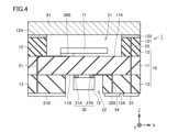
- FIG. 4 is a schematic cross-sectional view showing how the ceramic wiring member according to the first embodiment is used.
- FIG. 5 is a schematic cross-sectional view showing the structure of the ceramic wiring member in the second embodiment.
- FIG. 6 is a schematic cross-sectional view showing the structure of a ceramic wiring member in Embodiment 3.
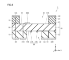
- FIG. 7 is a schematic plan view showing the structure of a ceramic wiring member in Embodiment 3.
- FIG. 1 is a schematic cross-sectional view showing the structure of a ceramic wiring member in Embodiment 1.
- FIG. 2 is a schematic plan view showing the structure of the ceramic wiring member in the first embodiment.
- FIG. 3 is a schematic plan view showing the structure of the
- FIG. 8 is a schematic plan view showing the structure of a ceramic wiring member in Embodiment 3.
- FIG. 9 is a schematic cross-sectional view showing the structure of a ceramic wiring member in Embodiment 4.
- FIG. 10 is a schematic cross-sectional view showing the structure of a ceramic wiring member in Embodiment 5.
- FIG. 11 is a schematic cross-sectional view showing the structure of a ceramic wiring member in Embodiment 6.
- FIG. 12 is a schematic plan view showing the structure of a ceramic wiring member in Embodiment 6.
- FIG. 13 is a schematic plan view showing the structure of a ceramic wiring member in Embodiment 6.
- FIG. 14 is a schematic cross-sectional view showing how the ceramic wiring member in Embodiment 6 is used.
- the ceramic wiring member of the present disclosure includes a main body and a conductive part that is arranged in contact with the main body and is made of a conductor.
- the main body has a flat plate shape, and includes a ceramic plate part, and a first frame part rising from the plate part so as to surround a first cavity, which is a space on the first main surface of the plate part.
- the first frame portion includes a conductive region arranged to include a first end surface located on the opposite side of the plate portion in the thickness direction of the plate portion.
- the main body part has a pair of parts that are part of the surface of the main body part, when the surface of the main body part located on the opposite side to the first end surface in the thickness direction of the plate part is viewed in plan in the thickness direction of the plate part.
- the device includes a first region and a pair of second regions that are part of the surface of the main body apart from the pair of first regions.
- the conductive part includes a pair of first external terminals arranged in contact with the main body so as to correspond to the pair of first regions, and a pair of first external terminals arranged in contact with the main body so as to correspond to the pair of second regions.
- a pair of second external terminals and a ground that is arranged in contact with the surface of the main body portion located on the opposite side to the first end surface in the thickness direction of the plate-like portion, separately from the first external terminal and the second external terminal.
- a pair of first internal terminals disposed in contact with the surface of the main body facing the first cavity; and a pair of second internal terminals disposed in contact with the main body apart from the pair of first internal terminals.
- the ground terminal is electrically connected to the conductive region without being electrically connected to the first external terminal, the second external terminal, the first internal terminal, and the second internal terminal.
- One of the pair of first external terminals is electrically connected to one of the pair of first internal terminals, and the other of the pair of first external terminals is electrically connected to the other of the pair of first internal terminals.
- One of the pair of second external terminals is electrically connected to one of the pair of second internal terminals, and the other of the pair of second external terminals is electrically connected to the other of the pair of second internal terminals.
- one of the pair of first external terminals is electrically connected to one of the pair of second internal terminals, and the other of the pair of first external terminals is electrically connected to the other of the pair of second internal terminals;
- One of the pair of second external terminals is electrically connected to one of the pair of first internal terminals, and the other of the pair of second external terminals is electrically connected to the other of the pair of first internal terminals.
- each internal terminal included in the first internal terminal and the second internal terminal and each external terminal included in the first external terminal and the second external terminal are electrically connected in a one-to-one relationship. connected. Therefore, by arranging the electronic components so as to be electrically connected to each of the first internal terminal and the second internal terminal, a plurality of electronic components can be mounted on the ceramic wiring member of the present disclosure.
- the first internal terminal is placed in contact with the surface of the main body facing the first cavity, by placing a metal lid on the first frame, the first internal terminal can be placed on top of the first internal terminal. An electronic component to be used can be sealed within the first cavity.
- the lid and the ground terminal are electrically connected via the conductive region, while the ground terminal is connected to the first external terminal, the second external terminal, and the ground terminal. Since it is not electrically connected to the first internal terminal and the second internal terminal, the signal passing through the electronic component wiring that connects the electronic component and the external terminal is not affected by the ground wiring. As a result, high stability of signals passing through the wiring for electronic components can be achieved.
- the ceramic wiring member of the present disclosure it is possible to mount a plurality of electronic components including an electronic component mounted in a cavity that can be sealed with a metal lid, and to connect the electronic components and external terminals. It is possible to provide a ceramic wiring member that can achieve high stability of signals passing through wiring for electronic components that connects.
- first frame including the first end surface may be a conductive region, or the entire first frame may be a conductive region.
- the ground terminal contacts the surface of the main body corresponding to one of the pair of first regions, and contacts one of the first external terminals of the pair of first external terminals. They may be placed adjacent to each other.
- the ground terminal and the first external terminal arranged adjacent to each other can be connected to the same terminal on the circuit board. It is possible to select the state in which the terminal is connected or the state in which it is connected to a different terminal. As a result, it is possible to obtain a ceramic wiring member that is compatible with circuit boards of a wide variety of designs.
- the main body portion includes a second cavity rising from the plate portion so as to surround a second cavity, which is a space on the second main surface located on the opposite side in the thickness direction from the first main surface of the plate portion. It may further include two frame parts.
- the pair of first internal terminals may be arranged in contact with the first main surface.
- the pair of second internal terminals may be arranged in contact with the second main surface.
- the conductive portion may further include a third internal terminal disposed on the first main surface apart from the pair of first internal terminals.
- the third internal terminal may be electrically connected to one of the pair of second internal terminals.
- the pair of second internal terminals may be arranged in contact with the surface of the main body facing the first cavity. This configuration allows two electronic components to be placed within the first cavity.
- the first frame has a frame-like shape surrounding the first cavity, and is located on the opposite side of the ceramic frame rising from the plate and the plate of the frame.
- a conductive layer as a conductive region disposed on the end surface may be included.
- the first frame portion may be made of metal.
- the first frame portion has a frame-like shape surrounding the first cavity, and has a ceramic first portion rising from the plate-like portion and a frame-like shape surrounding the first cavity. , and a second metal portion stacked on top of the first portion.
- FIG. 1 is a schematic cross-sectional view showing the structure of a ceramic wiring member in Embodiment 1.
- 2 and 3 are schematic plan views showing the structure of the ceramic wiring member in the first embodiment.
- FIG. 1 is a diagram corresponding to a cross section taken along line II in FIGS. 2 and 3.
- FIG. 4 is a schematic cross-sectional view showing how the ceramic wiring member according to the first embodiment is used. Note that in the following drawings, the positions and shapes of the wires are schematically expressed from the viewpoint of facilitating understanding of the manner in which the terminals are connected to each other by the wires.
- a ceramic wiring member 1 includes a main body 10 and a conductive part 30 made of a conductor and arranged in contact with the main body 10.
- the main body portion 10 includes a plate-like portion 11 , a first frame portion 12 , and a second frame portion 13 .
- the plate-shaped portion 11 is made of ceramic.
- the plate portion 11 has a flat plate shape.
- the planar shape of the plate-like portion 11 is not particularly limited, in this embodiment, the planar shape of the plate-like portion 11 (direction perpendicular to the first principal surface 11A; shape seen in the Z-axis direction) is a quadrilateral (rectangle) (see FIGS. 2 and 3).
- the first frame portion 12 is an annular portion rising from the first main surface 11A of the plate-shaped portion 11.
- the first frame portion 12 surrounds the first cavity 21, which is a space above the first main surface 11A of the plate-like portion 11.
- the shape of the first frame portion 12 when viewed in the Z-axis direction is a quadrangle (rectangle) along the outer peripheral surface of the plate-like portion 11 (see FIGS. 2 and 3).
- the second frame portion 13 is an annular portion rising from the second main surface 11B of the plate-shaped portion 11.
- the second frame portion 13 surrounds the second cavity 22, which is a space above the second main surface 11B of the plate-like portion 11.
- the second frame portion 13 is made of ceramic.
- the shape of the second frame portion 13 when viewed in the Z-axis direction is a quadrangle (rectangle) along the outer peripheral surface of the plate-like portion 11 (see FIGS. 2 and 3).
- the first frame part 12 has a frame shape surrounding the first cavity 21, and is located on the opposite side of the ceramic frame 121 rising from the plate part 11 and the plate part 11 of the frame 121.
- a conductive layer 122 as a conductive region disposed on the end face is included.
- the conductive layer 122 is arranged so as to include the first end surface 12A located on the opposite side to the plate-like part 11 in the thickness direction (Z-axis direction) of the plate-like part 11. That is, the conductive layer 122 constitutes the first end surface 12A.
- the ceramic that constitutes the plate portion 11, the frame 121, and the second frame portion 13 is not particularly limited, but aluminum oxide (Al 2 O 3 ) can be used, for example.
- the ceramic constituting the main body 10 is selected from the group consisting of silicon dioxide (SiO 2 ), calcium oxide (CaO), magnesium oxide (MgO), manganese oxide (MnO), and barium oxide (BaO) as a sintering aid. It may include at least one selected one.
- the main body part 10 has a surface of the main body part 10 when the surface of the main body part 10 located on the opposite side to the first end surface 12A in the thickness direction (Z-axis direction) of the plate-like part 11 is viewed planarly in the Z-axis direction.
- the first regions 131A, 131B and the second regions 132A, 132B are arranged at the corners of the second frame portion 13, which has a rectangular shape when viewed in the Z-axis direction.
- the pair of first regions 131A and 131B are arranged at diagonally located corners of the second frame portion 13 having a quadrangular shape.
- the pair of second regions 132A, 132B are located on the diagonal of the second frame portion 13 having a quadrangular shape, and are arranged at corners different from the corners where the pair of first regions 131A, 131B are arranged. ing.
- the conductive part 30 includes a first external input terminal 31A, a first external output terminal 31B, a second external input terminal 32A, a second external output terminal 32B, a ground terminal 33, and a first internal input terminal 36A. It includes a first internal output terminal 36B, a second internal input terminal 37A, and a second internal output terminal 37B.
- the first external input terminal 31A is arranged in contact with the end surface 13A of the second frame portion 13 on the opposite side to the plate-like portion 11 so as to correspond to one first region 131A.
- the first external output terminal 31B is arranged in contact with the end surface 13A of the second frame portion 13 so as to correspond to the other first region 131B.
- the second external input terminal 32A is arranged in contact with the end surface 13A of the second frame portion 13 so as to correspond to one second region 132A.
- the second external output terminal 32B is arranged in contact with the end surface 13A of the second frame portion 13 so as to correspond to the other second region 132B.
- the ground terminal 33 is arranged in contact with the end surface 13A of the second frame portion 13 so as to correspond to the other second region 132B.
- the ground terminal 33 is arranged adjacent to the second external output terminal 32B in a region corresponding to the other second region 132B. In this embodiment shown in FIG.
- the ground terminal 33 is arranged at a corner, and the second external output terminal 32B is on the side of the first external output terminal 31B when viewed from the ground terminal 33 (on the left side of the ground terminal 33 in FIG. 3). is located adjacent to.
- the second external output terminal 32B may be arranged at the corner, and the ground terminal 33 may be arranged to the left of the second external output terminal 32B.
- the first internal input terminal 36A and the first internal output terminal 36B as the first internal terminals are arranged in contact with the surface of the main body portion 10 facing the first cavity 21. More specifically, the first internal input terminal 36A and the first internal output terminal 36B are arranged in contact with the first main surface 11A of the plate-shaped portion 11.
- a second internal input terminal 37A and a second internal output terminal 37B serving as second internal terminals are arranged in contact with the main body 10 apart from the first internal input terminal 36A and the first internal output terminal 36B. More specifically, the second internal input terminal 37A and the second internal output terminal 37B are arranged in contact with the second main surface 11B of the plate-shaped portion 11.
- the ground terminal 33 includes a first external input terminal 31A, a first external output terminal 31B, a second external input terminal 32A, a second external output terminal 32B, a first internal input terminal 36A, a first internal output terminal 36B, and a second internal terminal. It is electrically connected to the conductive layer 122 by a wiring 55 as a ground wiring without being electrically connected to the input terminal 37A and the second internal output terminal 37B.
- the first internal input terminal 36A and the first external input terminal 31A are electrically connected by a wiring 52 as an electronic component wiring.
- the first internal output terminal 36B and the first external output terminal 31B are electrically connected by a wiring 51 as an electronic component wiring.
- the second internal input terminal 37A and the second external input terminal 32A are electrically connected by a wiring 53 as an electronic component wiring.
- the second internal output terminal 37B and the second external output terminal 32B are electrically connected by a wiring 54 as an electronic component wiring.
- the first internal input terminal 36A and the second external input terminal 32A are connected.
- the first internal output terminal 36B and the second external output terminal 32B may be electrically connected by electronic component wiring.
- the second internal input terminal 37A and the first external input terminal 31A may be electrically connected by electronic component wiring.
- the second internal output terminal 37B and the first external output terminal 31B may be electrically connected by electronic component wiring.
- the conductive part 30, the conductive layer 122, and the wirings 51, 52, 53, 54, and 55 are made of a conductor containing, for example, at least one of W (tungsten), Mo (molybdenum), and Cu (copper).
- each internal terminal 36A, 36B, 37A, 37B and each external terminal 31A, 31B, 32A, 32B are electrically connected in a one-to-one relationship. . Therefore, as shown in FIG. 4, for example, a crystal resonator 71, which is a piezoelectric vibrating element, can be placed on the first internal input terminal 36A and the first internal output terminal 36B. A voltage for causing the crystal resonator 71 to resonate is applied between external terminals 31A and 31B. Further, for example, a thermistor 72 can be placed on the second internal input terminal 37A and the second internal output terminal 37B. A voltage for measuring the resistance of thermistor 72 is applied between external terminals 32A and 32B.
- the ceramic wiring member 1 of this embodiment is a ceramic wiring member on which a plurality of electronic components can be mounted. Furthermore, by placing the metal lid 81 on the first end surface 12A of the first frame portion 12, the crystal resonator 71 can be hermetically sealed within the first cavity 21. Further, when the metal lid 81 is placed on the first end surface 12A of the first frame portion 12, the lid 81 and the ground terminal 33 are electrically connected via the conductive layer 122 and the wiring 55.
- the ground terminal 33 includes a first external input terminal 31A, a first external output terminal 31B, a second external input terminal 32A, a second external output terminal 32B, a first internal input terminal 36A, a first internal output terminal 36B, and a second It is not electrically connected to the internal input terminal 37A and the second internal output terminal 37B. Therefore, signals passing through the electronic component wirings 51, 52, 53, and 54 that connect the crystal oscillator 71 and thermistor 72 to the external terminals 31A, 31B, 32A, and 32B are not affected by the wiring 55 as the ground wiring. . As a result, it is possible to achieve high stability of signals passing through the electronic component wirings 51, 52, 53, and 54.
- the ceramic wiring member 1 of the present embodiment includes a plurality of electronic components (crystal resonator 71 and thermistor 72), and which connect electronic components (crystal oscillator 71 and thermistor 72) to external terminals 31A, 31B, 32A, 32B. It is a ceramic wiring member that can achieve high stability.
- lid 81 and the first end surface 12A (conductive layer 122) of the first frame portion 12 can be joined by any method such as welding, brazing, or pressure welding.
- the oscillation frequency of the crystal resonator 71 is affected by temperature. As shown in FIG. 4, by mounting a crystal oscillator 71 and a thermistor 72, which is an element for detecting temperature, on a single ceramic wiring member 1, the crystal oscillator 71 can be adjusted based on the temperature detected by the thermistor 72. By driving, the crystal resonator 71 can be operated appropriately.
- the ground terminal 33 is arranged adjacent to the second external output terminal 32B in a region corresponding to the other second region 132B.
- the ground terminal 33 and other terminals such as the second external output terminal 32B do not necessarily need to be arranged adjacently, but by arranging them adjacently in this way, the crystal resonator 71 and the thermistor
- the ceramic wiring member 1 of this embodiment is a ceramic wiring member that can be applied to circuit boards with a wide range of designs. Note that, with reference to FIG. 3, since the ground terminal 33 is arranged adjacent to the second external output terminal 32B in a region corresponding to the second region 132B, the area of the second external output terminal 32B as seen in the Z-axis direction is is smaller than other external terminals (first external input terminal 31A, first external output terminal 31B, second external input terminal 32A).
- the first external input terminal 31A and the first external output terminal 31B are connected to the crystal resonator 71. Since the first external input terminal 31A and the first external output terminal 31B maintain the same area as the conventional one, poor contact with the test terminal for checking the operation of the crystal resonator 71 is unlikely to occur.
- a green sheet to become the main body portion 10 is prepared. Specifically, at least one powder selected from the group consisting of Al 2 O 3 powder, which is the main component of the ceramic constituting the main body 10, and SiO 2 , CaO, MgO, MnO, and BaO, which is a sintering aid. The powder, resin, solvent, etc. are mixed in a ball mill to obtain a slurry. This slurry is processed into a green sheet by a doctor blade method. As a result, a green sheet to become the main body portion 10 is obtained.
- a green sheet to become the main body portion 10 is obtained.
- a plurality of green sheets each having a rectangular planar shape are prepared as the green sheets to become the plate-like portion 11.
- a plurality of green sheets to become the first frame portion 12 and the second frame portion 13 are also prepared.
- the green sheet to become the first frame part 12 and the second frame part 13 has a rectangular planar shape, and is an annular green sheet from which the part (center part) corresponding to the first cavity 21 and the second cavity 22 has been removed.
- a green sheet is prepared.
- pastes that will become the conductive portion 30, the conductive layer 122, and the wirings 51, 52, 53, 54, and 55 are printed on the prepared green sheet. Specifically, first, at least one metal component of W, Mo, and Cu is mixed with additives, resin, solvent, etc., and if necessary, ceramic powder is added and kneaded to form a paste. Create.
- the metal component may be a powder.
- This paste is printed on the previously prepared green sheet by, for example, screen printing.
- the conductive layer 122, and the wirings 51, 52, 53, 54, and 55 those that spread or extend within the XY plane are covered by green sheets.
- the above paste is printed on the surface, and for those extending in the Z-axis direction, a through hole is formed through the green sheet in the thickness direction, and the through hole is filled with the above paste.
- the green sheets printed with the paste are dried and laminated to obtain a laminate. Then, the ceramic wiring member 1 is obtained by firing this laminate.
- FIG. 5 is a schematic cross-sectional view showing the structure of the ceramic wiring member in the second embodiment.
- FIG. 5 is a diagram corresponding to FIG. 1 of the first embodiment.
- the ceramic wiring member 1 of the second embodiment basically has the same configuration as the first embodiment, has the same effects, and can be manufactured in the same manner. However, with reference to FIGS. 5 and 1, the ceramic wiring member 1 of the second embodiment is different from the ceramic wiring member 1 of the first embodiment in that additional terminals and wiring are provided. are different.
- the conductive portion 30 of the ceramic wiring member 1 of the second embodiment has a third conductive portion disposed on the first main surface 11A apart from the first internal input terminal 36A and the first internal output terminal 36B. It further includes an internal terminal 38.
- the third internal terminal 38 is electrically connected to one of the pair of second internal terminals 37A and 37B, more specifically to the second internal output terminal 37B, via a wiring 56.
- the third internal terminal 38 located on the first main surface 11A and the second internal output terminal 37B are electrically connected via the wiring 56.
- heat emitted from the crystal oscillator 71 disposed on the first internal input terminal 36A and the first internal output terminal 36B located on the first main surface 11A is transferred to the third internal terminal 38, the wiring 56 and It is transmitted to the thermistor 72 via the second internal output terminal 37B.
- the third internal terminal 38 may be electrically connected to the second internal input terminal 37A via wiring instead of the second internal output terminal 37B.
- the area of the third internal terminal 38 may be smaller than the sum of the area of the first internal input terminal 36A and the area of the first internal output terminal 36B. Since the heat capacity of the third internal terminal 38 is reduced, the temperature detection sensitivity of the crystal resonator 71 is increased.
- the area of the third internal terminal 38 may be smaller than the smaller area of the first internal input terminal 36A and the first internal output terminal 36B. With this configuration, the heat capacity of the third internal terminal 38 is reduced, so that the temperature detection sensitivity of the crystal resonator 71 is further increased.
- the electrical connection between the third internal terminal 38, the wiring 56, and the second internal output terminal 37B is not for the purpose of securing a current path as described above, but for the purpose of thermal connection. be.
- FIG. 6 is a schematic cross-sectional view showing the structure of a ceramic wiring member in Embodiment 3.
- 7 and 8 are schematic plan views showing the structure of a ceramic wiring member in Embodiment 3. 6,
- FIG. 7, and FIG. 8 are diagrams corresponding to FIG. 1, FIG. 2, and FIG. 3 in the first embodiment.
- the ceramic wiring member 1 of Embodiment 3 basically has the same configuration as Embodiment 1, exhibits the same effects, and can be manufactured in the same manner. However, with reference to FIGS. 6 to 8 and FIGS. 1 to 3, the ceramic wiring member 1 of the third embodiment is different from that of the first embodiment in the arrangement of the ground terminal 33 and the arrangement of the corresponding wiring. It's different.
- the ground terminal 33 is arranged adjacent to the first external output terminal 31B in a region corresponding to the other first region 131B. has been done. Referring to FIG. 8, since the ground terminal 33 is arranged adjacent to the first external output terminal 31B in the region corresponding to the first region 131B, the area of the first external output terminal 31B when viewed in the Z-axis direction is It is smaller than other external terminals (first external input terminal 31A, second external input terminal 32A, second external output terminal 32B).
- the ground terminals 33 include the first external input terminal 31A, the first external output terminal 31B, the second external input terminal 32A, the second external output terminal 32B, and the first internal input terminal 36A. , are not electrically connected to the first internal output terminal 36B, the second internal input terminal 37A, and the second internal output terminal 37B. Therefore, signals passing through the electronic component wirings 51, 52, 53, and 54 that connect the crystal oscillator 71 and thermistor 72 to the external terminals 31A, 31B, 32A, and 32B are not affected by the wiring 55 as the ground wiring. . As a result, it is possible to achieve high stability of signals passing through the electronic component wirings 51, 52, 53, and 54.
- the ceramic wiring member 1 of this embodiment includes a plurality of crystal oscillators 71 mounted in the first cavity 21 that can be sealed with a metal lid 81.
- Electronic component wiring 51, 52 that can mount electronic components (crystal oscillator 71 and thermistor 72) and connects the electronic components (crystal oscillator 71 and thermistor 72) to external terminals 31A, 31B, 32A, 32B.
- 53, 54 are ceramic wiring members that can achieve high stability of signals passing through them.
- FIG. 9 is a schematic cross-sectional view showing the structure of a ceramic wiring member in Embodiment 4.
- FIG. 9 is a diagram corresponding to FIG. 1 in the first embodiment.
- the ceramic wiring member 1 of Embodiment 4 basically has the same configuration as Embodiment 1, exhibits the same effects, and can be manufactured in the same manner. However, referring to FIG. 9 and FIG. 1, the ceramic wiring member 1 of the fourth embodiment differs from the first embodiment in the structure of the first frame portion.
- a metal frame 14 as a first frame portion is used instead of the frame 121 and the conductive layer 122 of the first embodiment.
- the first frame portion in this embodiment is made of metal.
- the entire first frame portion in this embodiment is a conductive region.
- the metal constituting the metal frame 14 is not particularly limited, but an alloy such as Kovar that has a small difference in coefficient of linear expansion from the ceramic constituting the main body 10 can be used.
- a conductive layer 122 is arranged in a ring shape along the outer periphery of the plate-like part 11.
- the wiring 55 as a ground wiring electrically connects the metal frame 14 and the ground terminal 33 via the conductive layer 122.
- the metal lid 81 on the first end surface 14A, which is the end surface of the metal frame 14 on the opposite side to the plate-like portion 11, electronic components (for example, the crystal resonator 71) can be mounted.
- the first cavity 21 can be hermetically sealed.
- the lid 81 and the ground terminal 33 are electrically connected via the metal frame 14, the conductive layer 122, and the wiring 55.
- the same effects as in the first embodiment can be obtained in the ceramic wiring member 1 adopting the structure of the present embodiment.
- FIG. 10 is a schematic cross-sectional view showing the structure of a ceramic wiring member in Embodiment 5.
- FIG. 10 is a diagram corresponding to FIG. 1 in the first embodiment.
- the ceramic wiring member 1 of Embodiment 5 basically has the same configuration as Embodiment 1, exhibits the same effects, and can be manufactured in the same manner. However, referring to FIG. 10 and FIG. 1, the ceramic wiring member 1 of the fifth embodiment differs from the first embodiment in the structure of the first frame portion.
- the first frame portion 12 in the ceramic wiring member 1 of the present embodiment has a frame-like shape surrounding the first cavity 21. It includes a frame 121 , a conductive layer 122 as a conductive region disposed on an end surface of the frame 121 opposite to the plate-like portion 11 , and a metal frame 14 laminated on the conductive layer 122 . That is, the first frame part 12 has a frame-like shape surrounding the first cavity, and includes a frame body 121 as a first ceramic part rising from the plate part 11 and a frame-shaped frame body surrounding the first cavity 21.
- the conductive layer 122 has a shape and includes a conductive layer 122 as a second metal part stacked on a frame body 121 and a metal frame 14 . Even with such a configuration, by arranging the metal lid 81 on the first end surface 12A (on the metal frame 14), which is the end surface of the first frame section 12 opposite to the plate-like section 11, electronic components can be protected. (For example, the crystal resonator 71) can be hermetically sealed within the first cavity 21. Furthermore, when the metal lid 81 is placed on the first end surface 12A, the lid 81 and the ground terminal 33 are electrically connected via the metal frame 14, the conductive layer 122, and the wiring 55. As a result, the same effects as in the first embodiment can be obtained in the ceramic wiring member 1 adopting the structure of the present embodiment.
- FIG. 11 is a schematic cross-sectional view showing the structure of a ceramic wiring member in Embodiment 6.
- 12 and 13 are schematic plan views showing the structure of a ceramic wiring member in Embodiment 6.
- FIG. 11 is a diagram corresponding to a cross section taken along line segment XI-XI in FIGS. 12 and 13.
- FIG. 14 is a schematic cross-sectional view showing how the ceramic wiring member in Embodiment 6 is used.
- the ceramic wiring member 1 of Embodiment 6 basically has the same configuration as Embodiment 1, exhibits the same effects, and can be manufactured in the same manner. However, referring to FIGS. 11 to 14 and FIGS. 1 to 4, the ceramic wiring member 1 of the sixth embodiment differs from the first embodiment in the arrangement of the frame and the arrangement of the internal terminals.
- the main body portion 10 of this embodiment includes a plate-like portion 11 and a first frame portion 12, but does not include a second frame portion 13.
- the first frame part 12 has a frame shape surrounding the first cavity 21, and includes a ceramic lower frame part 15 rising from the plate part 11, and an upper frame part laminated on the lower frame part 15.
- the upper frame 16 includes a ceramic frame 161 and a conductive layer 162 as a conductive region disposed on an end surface of the frame 161 opposite to the lower frame 15.
- the width of the lower frame portion 15 is larger than the width of the upper frame portion 16 when viewed in the Z-axis direction. As a result, a portion of the first main surface 11A of the plate-shaped portion 11 and the end surface 15A of the lower frame portion 15 on the side opposite to the plate-shaped portion 11 are exposed in the first cavity 21.
- the first internal input terminal 36A and the first internal output terminal 36B are arranged on the end surface 15A of the lower frame portion 15 exposed inside the first cavity 21.
- the second internal input terminal 37A and the second internal output terminal 37B are arranged on the first main surface 11A of the plate-shaped portion 11 exposed inside the first cavity 21. That is, the first internal input terminal 36A and the first internal output terminal 36B are arranged in contact with the surface of the main body portion 10 facing the first cavity 21.
- the main body part 10 has a surface of the main body part 10 when the surface of the main body part 10 located on the opposite side to the first end surface 12A in the thickness direction (Z-axis direction) of the plate-like part 11 is viewed planarly in the Z-axis direction.
- the arrangement of the first regions 131A, 131B and the second regions 132A, 132B when viewed in the Z-axis direction is the same as in the first embodiment, but since the second frame portion 13 is not present in this embodiment,
- the first regions 131A, 131B and the second regions 132A, 132B are arranged at the corners of the plate-shaped portion 11.
- the first external input terminal 31A, the first external output terminal 31B, the second external input terminal 32A, the second external output terminal 32B, and the ground terminal 33 are connected to the first regions 131A, 131B and It is arranged in contact with the second main surface 11B of the plate-shaped portion 11 so as to correspond to the second regions 132A and 132B.
- the first internal input terminal 36A, the first internal output terminal 36B, the second internal input terminal 37A, the second internal output terminal 37B, the first external input terminal 31A, the first external output terminal 31B, the second external input terminal 32A and the second external output terminal 32B are electrically connected by wires 51, 52, 53, and 54 as electronic component wires, as in the first embodiment.
- the ground terminal 33 and the conductive layer 162 are electrically connected by a wiring 55 serving as a ground wiring.
- each internal terminal 36A, 36B, 37A, 37B and each external terminal 31A, 31B, 32A, 32B are electrically connected in a one-to-one relationship. . Therefore, as shown in FIG. 14, for example, a crystal resonator 71 can be placed on the first internal input terminal 36A and the first internal output terminal 36B. Further, for example, a thermistor 72 can be placed on the second internal input terminal 37A and the second internal output terminal 37B. In this way, the ceramic wiring member 1 of this embodiment is a ceramic wiring member on which a plurality of electronic components can be mounted.
- the metal lid 81 on the first end surface 12A of the first frame portion 12, the crystal resonator 71 and the thermistor 72 can be hermetically sealed within the first cavity 21. Furthermore, when the metal lid 81 is placed on the first end surface 12A of the first frame portion 12, the lid 81 and the ground terminal 33 are electrically connected via the conductive layer 162 and the wiring 55.
- the ground terminal 33 includes a first external input terminal 31A, a first external output terminal 31B, a second external input terminal 32A, a second external output terminal 32B, a first internal input terminal 36A, a first internal output terminal 36B, and a second It is not electrically connected to the internal input terminal 37A and the second internal output terminal 37B.
- the ceramic wiring member 1 of the present embodiment is equipped with a plurality of electronic components including the crystal resonator 71 and thermistor 72 mounted in the first cavity 21 that can be sealed with the metal lid 81.
- the crystal resonator 71 and the thermistor 72 are illustrated as examples of electronic components that can be mounted on the ceramic wiring member 1, but the electronic components that can be mounted on the ceramic wiring member of the present disclosure are limited to these. I can't do it.
- an integrated circuit instead of the thermistor 72, an integrated circuit (IC) may be mounted on the second internal terminals 37A, 37B of the ceramic wiring member 1.
- the IC may have a built-in thermistor.
- the second internal terminals 37A, 37B may be connected to a thermistor.
- 1 Ceramic wiring member 10 Main body part, 11 Plate part, 11A first main surface, 11B second main surface, 12 First frame part, 12A First end face, 13 Second frame part, 13A End face, 14 Metal frame, 14A first end surface, 15 lower frame section, 15A end surface, 16 upper frame section, 21 first cavity, 22 second cavity, 30 conductive section, 31A first external input terminal, 31B first external output terminal, 32A second External input terminal, 32B second external output terminal, 33 ground terminal, 36A first internal input terminal, 36B first internal output terminal, 37A second internal input terminal, 37B second internal output terminal, 38 third internal terminal, 51 ⁇ 56 wiring, 71 crystal resonator, 72 thermistor, 81 lid, 121 frame, 122 conductive layer, 131A, 131B first region, 132A, 132B second region, 161 frame, 162 conductive layer.
Landscapes
- Engineering & Computer Science (AREA)
- Microelectronics & Electronic Packaging (AREA)
- Manufacturing & Machinery (AREA)
- Piezo-Electric Or Mechanical Vibrators, Or Delay Or Filter Circuits (AREA)
- Production Of Multi-Layered Print Wiring Board (AREA)
- Structure Of Printed Boards (AREA)
- Details Of Connecting Devices For Male And Female Coupling (AREA)
Priority Applications (3)
| Application Number | Priority Date | Filing Date | Title |
|---|---|---|---|
| CN202380011605.8A CN117322140A (zh) | 2022-04-28 | 2023-04-27 | 陶瓷布线构件 |
| JP2024518021A JP7557107B2 (ja) | 2022-04-28 | 2023-04-27 | セラミック配線部材 |
| TW112115932A TWI852518B (zh) | 2022-04-28 | 2023-04-28 | 陶瓷配線構件 |
Applications Claiming Priority (2)
| Application Number | Priority Date | Filing Date | Title |
|---|---|---|---|
| JPPCT/JP2022/019340 | 2022-04-28 | ||
| JP2022019340 | 2022-04-28 |
Publications (1)
| Publication Number | Publication Date |
|---|---|
| WO2023210735A1 true WO2023210735A1 (ja) | 2023-11-02 |
Family
ID=88518797
Family Applications (1)
| Application Number | Title | Priority Date | Filing Date |
|---|---|---|---|
| PCT/JP2023/016613 Ceased WO2023210735A1 (ja) | 2022-04-28 | 2023-04-27 | セラミック配線部材 |
Country Status (4)
| Country | Link |
|---|---|
| JP (1) | JP7557107B2 (https=) |
| CN (1) | CN117322140A (https=) |
| TW (1) | TWI852518B (https=) |
| WO (1) | WO2023210735A1 (https=) |
Citations (4)
| Publication number | Priority date | Publication date | Assignee | Title |
|---|---|---|---|---|
| JPH0766009A (ja) * | 1993-08-30 | 1995-03-10 | Mitsubishi Materials Corp | サーミスタ素子及びその製造方法 |
| JP2010035078A (ja) * | 2008-07-31 | 2010-02-12 | Kyocera Kinseki Corp | 圧電発振器 |
| JP2010073847A (ja) * | 2008-09-18 | 2010-04-02 | Sony Corp | Ptcサーミスタ素子及びその製造方法、並びに2次電池セル及びその製造方法 |
| WO2016080075A1 (ja) * | 2014-11-21 | 2016-05-26 | 株式会社大真空 | 圧電振動デバイス |
Family Cites Families (1)
| Publication number | Priority date | Publication date | Assignee | Title |
|---|---|---|---|---|
| CN111180572A (zh) * | 2015-03-11 | 2020-05-19 | 株式会社大真空 | 压电器件 |
-
2023
- 2023-04-27 WO PCT/JP2023/016613 patent/WO2023210735A1/ja not_active Ceased
- 2023-04-27 CN CN202380011605.8A patent/CN117322140A/zh active Pending
- 2023-04-27 JP JP2024518021A patent/JP7557107B2/ja active Active
- 2023-04-28 TW TW112115932A patent/TWI852518B/zh active
Patent Citations (4)
| Publication number | Priority date | Publication date | Assignee | Title |
|---|---|---|---|---|
| JPH0766009A (ja) * | 1993-08-30 | 1995-03-10 | Mitsubishi Materials Corp | サーミスタ素子及びその製造方法 |
| JP2010035078A (ja) * | 2008-07-31 | 2010-02-12 | Kyocera Kinseki Corp | 圧電発振器 |
| JP2010073847A (ja) * | 2008-09-18 | 2010-04-02 | Sony Corp | Ptcサーミスタ素子及びその製造方法、並びに2次電池セル及びその製造方法 |
| WO2016080075A1 (ja) * | 2014-11-21 | 2016-05-26 | 株式会社大真空 | 圧電振動デバイス |
Also Published As
| Publication number | Publication date |
|---|---|
| CN117322140A (zh) | 2023-12-29 |
| JPWO2023210735A1 (https=) | 2023-11-02 |
| JP7557107B2 (ja) | 2024-09-26 |
| TWI852518B (zh) | 2024-08-11 |
| TW202408325A (zh) | 2024-02-16 |
Similar Documents
| Publication | Publication Date | Title |
|---|---|---|
| TWI466437B (zh) | Piezoelectric vibrator | |
| JP5806096B2 (ja) | 圧電デバイス | |
| US20180309044A1 (en) | Piezoelectric resonator device | |
| JP2011030198A (ja) | 積層型の水晶振動子 | |
| JP2012142691A (ja) | 圧電デバイス | |
| US10334740B2 (en) | Electronic-component mount substrate, electronic device, and electronic module | |
| JP2010062959A (ja) | 表面実装型圧電発振器およびその特性測定方法 | |
| US20240413805A1 (en) | Thermistor-mounting piezoelectric resonator device | |
| JP7557107B2 (ja) | セラミック配線部材 | |
| CN113692644B (zh) | 电子部件收纳用封装件、电子装置以及电子模块 | |
| US20050225406A1 (en) | Temperature-compensated quartz-crystal oscillator | |
| JP2005020546A (ja) | 表面実装型水晶発振器 | |
| JP4479413B2 (ja) | 圧電発振器 | |
| JP2013110214A (ja) | 電子部品収納用パッケージ | |
| EP1309031B1 (en) | Nonreciprocal circuit device and communication apparatus | |
| CN207868186U (zh) | 电子部件收纳用封装件、电子装置及电子模块 | |
| JP4404684B2 (ja) | 配線基板 | |
| JP2007158419A (ja) | 表面実装用水晶発振器 | |
| JP6573515B2 (ja) | セラミック基板 | |
| JP4688673B2 (ja) | 電子部品搭載用絶縁基体および電子装置 | |
| JP7615294B2 (ja) | セラミック配線部材 | |
| US10388628B2 (en) | Electronic component package | |
| JP2004297209A (ja) | 表面実装型圧電発振器 | |
| JP2011223425A (ja) | 電子部品素子収納用パッケージ | |
| JP2010129564A (ja) | 電子部品パッケージ、及び圧電振動子 |
Legal Events
| Date | Code | Title | Description |
|---|---|---|---|
| WWE | Wipo information: entry into national phase |
Ref document number: 202380011605.8 Country of ref document: CN |
|
| WWE | Wipo information: entry into national phase |
Ref document number: 2024518021 Country of ref document: JP |
|
| 121 | Ep: the epo has been informed by wipo that ep was designated in this application |
Ref document number: 23796471 Country of ref document: EP Kind code of ref document: A1 |
|
| NENP | Non-entry into the national phase |
Ref country code: DE |
|
| 122 | Ep: pct application non-entry in european phase |
Ref document number: 23796471 Country of ref document: EP Kind code of ref document: A1 |