WO2023210735A1 - Ceramic wiring member - Google Patents
Ceramic wiring member Download PDFInfo
- Publication number
- WO2023210735A1 WO2023210735A1 PCT/JP2023/016613 JP2023016613W WO2023210735A1 WO 2023210735 A1 WO2023210735 A1 WO 2023210735A1 JP 2023016613 W JP2023016613 W JP 2023016613W WO 2023210735 A1 WO2023210735 A1 WO 2023210735A1
- Authority
- WO
- WIPO (PCT)
- Prior art keywords
- pair
- internal
- terminals
- terminal
- main body
- Prior art date
Links
- 239000000919 ceramic Substances 0.000 title claims abstract description 126
- 229910052751 metal Inorganic materials 0.000 claims description 40
- 239000002184 metal Substances 0.000 claims description 40
- 230000000630 rising effect Effects 0.000 claims description 14
- 239000004020 conductor Substances 0.000 claims description 5
- 239000013078 crystal Substances 0.000 description 35
- 230000000694 effects Effects 0.000 description 7
- 238000010586 diagram Methods 0.000 description 6
- AMWRITDGCCNYAT-UHFFFAOYSA-L hydroxy(oxo)manganese;manganese Chemical compound [Mn].O[Mn]=O.O[Mn]=O AMWRITDGCCNYAT-UHFFFAOYSA-L 0.000 description 6
- 239000000843 powder Substances 0.000 description 5
- QVQLCTNNEUAWMS-UHFFFAOYSA-N barium oxide Chemical compound [Ba]=O QVQLCTNNEUAWMS-UHFFFAOYSA-N 0.000 description 3
- 239000010949 copper Substances 0.000 description 3
- 239000000395 magnesium oxide Substances 0.000 description 3
- CPLXHLVBOLITMK-UHFFFAOYSA-N magnesium oxide Inorganic materials [Mg]=O CPLXHLVBOLITMK-UHFFFAOYSA-N 0.000 description 3
- AXZKOIWUVFPNLO-UHFFFAOYSA-N magnesium;oxygen(2-) Chemical compound [O-2].[Mg+2] AXZKOIWUVFPNLO-UHFFFAOYSA-N 0.000 description 3
- 238000000034 method Methods 0.000 description 3
- 229910018072 Al 2 O 3 Inorganic materials 0.000 description 2
- ODINCKMPIJJUCX-UHFFFAOYSA-N Calcium oxide Chemical compound [Ca]=O ODINCKMPIJJUCX-UHFFFAOYSA-N 0.000 description 2
- 229910004298 SiO 2 Inorganic materials 0.000 description 2
- VYPSYNLAJGMNEJ-UHFFFAOYSA-N Silicium dioxide Chemical compound O=[Si]=O VYPSYNLAJGMNEJ-UHFFFAOYSA-N 0.000 description 2
- 229910052802 copper Inorganic materials 0.000 description 2
- 238000001514 detection method Methods 0.000 description 2
- 238000004519 manufacturing process Methods 0.000 description 2
- 239000000463 material Substances 0.000 description 2
- 229910052750 molybdenum Inorganic materials 0.000 description 2
- 230000002093 peripheral effect Effects 0.000 description 2
- 239000011347 resin Substances 0.000 description 2
- 229920005989 resin Polymers 0.000 description 2
- 230000035945 sensitivity Effects 0.000 description 2
- 238000005245 sintering Methods 0.000 description 2
- 239000002002 slurry Substances 0.000 description 2
- 239000002904 solvent Substances 0.000 description 2
- 229910052721 tungsten Inorganic materials 0.000 description 2
- 238000003466 welding Methods 0.000 description 2
- RYGMFSIKBFXOCR-UHFFFAOYSA-N Copper Chemical compound [Cu] RYGMFSIKBFXOCR-UHFFFAOYSA-N 0.000 description 1
- ZOKXTWBITQBERF-UHFFFAOYSA-N Molybdenum Chemical compound [Mo] ZOKXTWBITQBERF-UHFFFAOYSA-N 0.000 description 1
- 239000000654 additive Substances 0.000 description 1
- 239000000956 alloy Substances 0.000 description 1
- 229910045601 alloy Inorganic materials 0.000 description 1
- 238000005219 brazing Methods 0.000 description 1
- BRPQOXSCLDDYGP-UHFFFAOYSA-N calcium oxide Chemical compound [O-2].[Ca+2] BRPQOXSCLDDYGP-UHFFFAOYSA-N 0.000 description 1
- 239000000292 calcium oxide Substances 0.000 description 1
- 230000007547 defect Effects 0.000 description 1
- 238000007606 doctor blade method Methods 0.000 description 1
- 238000010304 firing Methods 0.000 description 1
- 229910000833 kovar Inorganic materials 0.000 description 1
- 230000007257 malfunction Effects 0.000 description 1
- 239000011733 molybdenum Substances 0.000 description 1
- 230000010355 oscillation Effects 0.000 description 1
- TWNQGVIAIRXVLR-UHFFFAOYSA-N oxo(oxoalumanyloxy)alumane Chemical compound O=[Al]O[Al]=O TWNQGVIAIRXVLR-UHFFFAOYSA-N 0.000 description 1
- 238000007650 screen-printing Methods 0.000 description 1
- 239000000377 silicon dioxide Substances 0.000 description 1
- 235000012239 silicon dioxide Nutrition 0.000 description 1
- WFKWXMTUELFFGS-UHFFFAOYSA-N tungsten Chemical compound [W] WFKWXMTUELFFGS-UHFFFAOYSA-N 0.000 description 1
- 239000010937 tungsten Substances 0.000 description 1
Images


Classifications
-
- H—ELECTRICITY
- H05—ELECTRIC TECHNIQUES NOT OTHERWISE PROVIDED FOR
- H05K—PRINTED CIRCUITS; CASINGS OR CONSTRUCTIONAL DETAILS OF ELECTRIC APPARATUS; MANUFACTURE OF ASSEMBLAGES OF ELECTRICAL COMPONENTS
- H05K1/00—Printed circuits
- H05K1/02—Details
-
- H—ELECTRICITY
- H05—ELECTRIC TECHNIQUES NOT OTHERWISE PROVIDED FOR
- H05K—PRINTED CIRCUITS; CASINGS OR CONSTRUCTIONAL DETAILS OF ELECTRIC APPARATUS; MANUFACTURE OF ASSEMBLAGES OF ELECTRICAL COMPONENTS
- H05K3/00—Apparatus or processes for manufacturing printed circuits
- H05K3/46—Manufacturing multilayer circuits
Definitions
- the present disclosure relates to a ceramic wiring member.
- Ceramic wiring members that can mount a plurality of electronic components are known (for example, see Patent Document 1).
- the ceramic wiring member of Patent Document 1 is equipped with a crystal resonator and a thermistor.
- the crystal resonator is placed in a cavity sealed with a metal lid.
- a plurality of external terminals corresponding to each of the crystal resonator and thermistor are formed on the ceramic wiring member.
- Each of the crystal resonator and thermistor is connected to an external terminal via a plurality of electronic component wirings.
- the lid and the external terminal are connected via ground wiring. At this time, the ground wiring is connected to any one of the plurality of electronic component wirings.
- the ground wiring that connects the metal lid and the external terminal is connected to one of the plurality of electronic component wirings. Therefore, signals passing through the electronic component wiring connected to the ground wiring may be affected by the ground wiring and may become unstable.
- a ceramic wiring member includes a main body and a conductive part that is arranged in contact with the main body and is made of a conductor.
- the main body has a flat plate shape, and includes a ceramic plate part, and a first frame part rising from the plate part so as to surround a first cavity, which is a space on the first main surface of the plate part. ,including.
- the first frame portion includes a conductive region arranged to include a first end surface located on the opposite side of the plate portion in the thickness direction of the plate portion.
- the main body part has a pair of parts that are part of the surface of the main body part, when the surface of the main body part located on the opposite side to the first end surface in the thickness direction of the plate part is viewed in plan in the thickness direction of the plate part.
- the device includes a first region and a pair of second regions that are part of the surface of the main body apart from the pair of first regions.
- the conductive part includes a pair of first external terminals arranged in contact with the main body so as to correspond to the pair of first regions, and a pair of first external terminals arranged in contact with the main body so as to correspond to the pair of second regions.
- a pair of second external terminals and a ground that is arranged in contact with the surface of the main body portion located on the opposite side to the first end surface in the thickness direction of the plate-like portion, separately from the first external terminal and the second external terminal.
- a pair of first internal terminals disposed in contact with the surface of the main body facing the first cavity; and a pair of second internal terminals disposed in contact with the main body apart from the pair of first internal terminals.
- the ground terminal is electrically connected to the conductive region without being electrically connected to the first external terminal, the second external terminal, the first internal terminal, and the second internal terminal.
- One of the pair of first external terminals is electrically connected to one of the pair of first internal terminals, and the other of the pair of first external terminals is electrically connected to the other of the pair of first internal terminals.
- One of the pair of second external terminals is electrically connected to one of the pair of second internal terminals, and the other of the pair of second external terminals is electrically connected to the other of the pair of second internal terminals.
- one of the pair of first external terminals is electrically connected to one of the pair of second internal terminals, and the other of the pair of first external terminals is electrically connected to the other of the pair of second internal terminals;
- One of the pair of second external terminals is electrically connected to one of the pair of first internal terminals, and the other of the pair of second external terminals is electrically connected to the other of the pair of first internal terminals.
- the above ceramic wiring member it is possible to mount a plurality of electronic components including an electronic component mounted in a cavity that can be sealed with a metal lid, and the wiring for electronic components connects the electronic components and external terminals. It is possible to provide a ceramic wiring member that can achieve high stability of signals passing through the ceramic wiring member.
- FIG. 1 is a schematic cross-sectional view showing the structure of a ceramic wiring member in Embodiment 1.
- FIG. 2 is a schematic plan view showing the structure of the ceramic wiring member in the first embodiment.
- FIG. 3 is a schematic plan view showing the structure of the ceramic wiring member in the first embodiment.
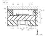
- FIG. 4 is a schematic cross-sectional view showing how the ceramic wiring member according to the first embodiment is used.
- FIG. 5 is a schematic cross-sectional view showing the structure of the ceramic wiring member in the second embodiment.
- FIG. 6 is a schematic cross-sectional view showing the structure of a ceramic wiring member in Embodiment 3.
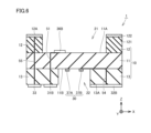
- FIG. 7 is a schematic plan view showing the structure of a ceramic wiring member in Embodiment 3.
- FIG. 1 is a schematic cross-sectional view showing the structure of a ceramic wiring member in Embodiment 1.
- FIG. 2 is a schematic plan view showing the structure of the ceramic wiring member in the first embodiment.
- FIG. 3 is a schematic plan view showing the structure of the
- FIG. 8 is a schematic plan view showing the structure of a ceramic wiring member in Embodiment 3.
- FIG. 9 is a schematic cross-sectional view showing the structure of a ceramic wiring member in Embodiment 4.
- FIG. 10 is a schematic cross-sectional view showing the structure of a ceramic wiring member in Embodiment 5.
- FIG. 11 is a schematic cross-sectional view showing the structure of a ceramic wiring member in Embodiment 6.
- FIG. 12 is a schematic plan view showing the structure of a ceramic wiring member in Embodiment 6.
- FIG. 13 is a schematic plan view showing the structure of a ceramic wiring member in Embodiment 6.
- FIG. 14 is a schematic cross-sectional view showing how the ceramic wiring member in Embodiment 6 is used.
- the ceramic wiring member of the present disclosure includes a main body and a conductive part that is arranged in contact with the main body and is made of a conductor.
- the main body has a flat plate shape, and includes a ceramic plate part, and a first frame part rising from the plate part so as to surround a first cavity, which is a space on the first main surface of the plate part.
- the first frame portion includes a conductive region arranged to include a first end surface located on the opposite side of the plate portion in the thickness direction of the plate portion.
- the main body part has a pair of parts that are part of the surface of the main body part, when the surface of the main body part located on the opposite side to the first end surface in the thickness direction of the plate part is viewed in plan in the thickness direction of the plate part.
- the device includes a first region and a pair of second regions that are part of the surface of the main body apart from the pair of first regions.
- the conductive part includes a pair of first external terminals arranged in contact with the main body so as to correspond to the pair of first regions, and a pair of first external terminals arranged in contact with the main body so as to correspond to the pair of second regions.
- a pair of second external terminals and a ground that is arranged in contact with the surface of the main body portion located on the opposite side to the first end surface in the thickness direction of the plate-like portion, separately from the first external terminal and the second external terminal.
- a pair of first internal terminals disposed in contact with the surface of the main body facing the first cavity; and a pair of second internal terminals disposed in contact with the main body apart from the pair of first internal terminals.
- the ground terminal is electrically connected to the conductive region without being electrically connected to the first external terminal, the second external terminal, the first internal terminal, and the second internal terminal.
- One of the pair of first external terminals is electrically connected to one of the pair of first internal terminals, and the other of the pair of first external terminals is electrically connected to the other of the pair of first internal terminals.
- One of the pair of second external terminals is electrically connected to one of the pair of second internal terminals, and the other of the pair of second external terminals is electrically connected to the other of the pair of second internal terminals.
- one of the pair of first external terminals is electrically connected to one of the pair of second internal terminals, and the other of the pair of first external terminals is electrically connected to the other of the pair of second internal terminals;
- One of the pair of second external terminals is electrically connected to one of the pair of first internal terminals, and the other of the pair of second external terminals is electrically connected to the other of the pair of first internal terminals.
- each internal terminal included in the first internal terminal and the second internal terminal and each external terminal included in the first external terminal and the second external terminal are electrically connected in a one-to-one relationship. connected. Therefore, by arranging the electronic components so as to be electrically connected to each of the first internal terminal and the second internal terminal, a plurality of electronic components can be mounted on the ceramic wiring member of the present disclosure.
- the first internal terminal is placed in contact with the surface of the main body facing the first cavity, by placing a metal lid on the first frame, the first internal terminal can be placed on top of the first internal terminal. An electronic component to be used can be sealed within the first cavity.
- the lid and the ground terminal are electrically connected via the conductive region, while the ground terminal is connected to the first external terminal, the second external terminal, and the ground terminal. Since it is not electrically connected to the first internal terminal and the second internal terminal, the signal passing through the electronic component wiring that connects the electronic component and the external terminal is not affected by the ground wiring. As a result, high stability of signals passing through the wiring for electronic components can be achieved.
- the ceramic wiring member of the present disclosure it is possible to mount a plurality of electronic components including an electronic component mounted in a cavity that can be sealed with a metal lid, and to connect the electronic components and external terminals. It is possible to provide a ceramic wiring member that can achieve high stability of signals passing through wiring for electronic components that connects.
- first frame including the first end surface may be a conductive region, or the entire first frame may be a conductive region.
- the ground terminal contacts the surface of the main body corresponding to one of the pair of first regions, and contacts one of the first external terminals of the pair of first external terminals. They may be placed adjacent to each other.
- the ground terminal and the first external terminal arranged adjacent to each other can be connected to the same terminal on the circuit board. It is possible to select the state in which the terminal is connected or the state in which it is connected to a different terminal. As a result, it is possible to obtain a ceramic wiring member that is compatible with circuit boards of a wide variety of designs.
- the main body portion includes a second cavity rising from the plate portion so as to surround a second cavity, which is a space on the second main surface located on the opposite side in the thickness direction from the first main surface of the plate portion. It may further include two frame parts.
- the pair of first internal terminals may be arranged in contact with the first main surface.
- the pair of second internal terminals may be arranged in contact with the second main surface.
- the conductive portion may further include a third internal terminal disposed on the first main surface apart from the pair of first internal terminals.
- the third internal terminal may be electrically connected to one of the pair of second internal terminals.
- the pair of second internal terminals may be arranged in contact with the surface of the main body facing the first cavity. This configuration allows two electronic components to be placed within the first cavity.
- the first frame has a frame-like shape surrounding the first cavity, and is located on the opposite side of the ceramic frame rising from the plate and the plate of the frame.
- a conductive layer as a conductive region disposed on the end surface may be included.
- the first frame portion may be made of metal.
- the first frame portion has a frame-like shape surrounding the first cavity, and has a ceramic first portion rising from the plate-like portion and a frame-like shape surrounding the first cavity. , and a second metal portion stacked on top of the first portion.
- FIG. 1 is a schematic cross-sectional view showing the structure of a ceramic wiring member in Embodiment 1.
- 2 and 3 are schematic plan views showing the structure of the ceramic wiring member in the first embodiment.
- FIG. 1 is a diagram corresponding to a cross section taken along line II in FIGS. 2 and 3.
- FIG. 4 is a schematic cross-sectional view showing how the ceramic wiring member according to the first embodiment is used. Note that in the following drawings, the positions and shapes of the wires are schematically expressed from the viewpoint of facilitating understanding of the manner in which the terminals are connected to each other by the wires.
- a ceramic wiring member 1 includes a main body 10 and a conductive part 30 made of a conductor and arranged in contact with the main body 10.
- the main body portion 10 includes a plate-like portion 11 , a first frame portion 12 , and a second frame portion 13 .
- the plate-shaped portion 11 is made of ceramic.
- the plate portion 11 has a flat plate shape.
- the planar shape of the plate-like portion 11 is not particularly limited, in this embodiment, the planar shape of the plate-like portion 11 (direction perpendicular to the first principal surface 11A; shape seen in the Z-axis direction) is a quadrilateral (rectangle) (see FIGS. 2 and 3).
- the first frame portion 12 is an annular portion rising from the first main surface 11A of the plate-shaped portion 11.
- the first frame portion 12 surrounds the first cavity 21, which is a space above the first main surface 11A of the plate-like portion 11.
- the shape of the first frame portion 12 when viewed in the Z-axis direction is a quadrangle (rectangle) along the outer peripheral surface of the plate-like portion 11 (see FIGS. 2 and 3).
- the second frame portion 13 is an annular portion rising from the second main surface 11B of the plate-shaped portion 11.
- the second frame portion 13 surrounds the second cavity 22, which is a space above the second main surface 11B of the plate-like portion 11.
- the second frame portion 13 is made of ceramic.
- the shape of the second frame portion 13 when viewed in the Z-axis direction is a quadrangle (rectangle) along the outer peripheral surface of the plate-like portion 11 (see FIGS. 2 and 3).
- the first frame part 12 has a frame shape surrounding the first cavity 21, and is located on the opposite side of the ceramic frame 121 rising from the plate part 11 and the plate part 11 of the frame 121.
- a conductive layer 122 as a conductive region disposed on the end face is included.
- the conductive layer 122 is arranged so as to include the first end surface 12A located on the opposite side to the plate-like part 11 in the thickness direction (Z-axis direction) of the plate-like part 11. That is, the conductive layer 122 constitutes the first end surface 12A.
- the ceramic that constitutes the plate portion 11, the frame 121, and the second frame portion 13 is not particularly limited, but aluminum oxide (Al 2 O 3 ) can be used, for example.
- the ceramic constituting the main body 10 is selected from the group consisting of silicon dioxide (SiO 2 ), calcium oxide (CaO), magnesium oxide (MgO), manganese oxide (MnO), and barium oxide (BaO) as a sintering aid. It may include at least one selected one.
- the main body part 10 has a surface of the main body part 10 when the surface of the main body part 10 located on the opposite side to the first end surface 12A in the thickness direction (Z-axis direction) of the plate-like part 11 is viewed planarly in the Z-axis direction.
- the first regions 131A, 131B and the second regions 132A, 132B are arranged at the corners of the second frame portion 13, which has a rectangular shape when viewed in the Z-axis direction.
- the pair of first regions 131A and 131B are arranged at diagonally located corners of the second frame portion 13 having a quadrangular shape.
- the pair of second regions 132A, 132B are located on the diagonal of the second frame portion 13 having a quadrangular shape, and are arranged at corners different from the corners where the pair of first regions 131A, 131B are arranged. ing.
- the conductive part 30 includes a first external input terminal 31A, a first external output terminal 31B, a second external input terminal 32A, a second external output terminal 32B, a ground terminal 33, and a first internal input terminal 36A. It includes a first internal output terminal 36B, a second internal input terminal 37A, and a second internal output terminal 37B.
- the first external input terminal 31A is arranged in contact with the end surface 13A of the second frame portion 13 on the opposite side to the plate-like portion 11 so as to correspond to one first region 131A.
- the first external output terminal 31B is arranged in contact with the end surface 13A of the second frame portion 13 so as to correspond to the other first region 131B.
- the second external input terminal 32A is arranged in contact with the end surface 13A of the second frame portion 13 so as to correspond to one second region 132A.
- the second external output terminal 32B is arranged in contact with the end surface 13A of the second frame portion 13 so as to correspond to the other second region 132B.
- the ground terminal 33 is arranged in contact with the end surface 13A of the second frame portion 13 so as to correspond to the other second region 132B.
- the ground terminal 33 is arranged adjacent to the second external output terminal 32B in a region corresponding to the other second region 132B. In this embodiment shown in FIG.
- the ground terminal 33 is arranged at a corner, and the second external output terminal 32B is on the side of the first external output terminal 31B when viewed from the ground terminal 33 (on the left side of the ground terminal 33 in FIG. 3). is located adjacent to.
- the second external output terminal 32B may be arranged at the corner, and the ground terminal 33 may be arranged to the left of the second external output terminal 32B.
- the first internal input terminal 36A and the first internal output terminal 36B as the first internal terminals are arranged in contact with the surface of the main body portion 10 facing the first cavity 21. More specifically, the first internal input terminal 36A and the first internal output terminal 36B are arranged in contact with the first main surface 11A of the plate-shaped portion 11.
- a second internal input terminal 37A and a second internal output terminal 37B serving as second internal terminals are arranged in contact with the main body 10 apart from the first internal input terminal 36A and the first internal output terminal 36B. More specifically, the second internal input terminal 37A and the second internal output terminal 37B are arranged in contact with the second main surface 11B of the plate-shaped portion 11.
- the ground terminal 33 includes a first external input terminal 31A, a first external output terminal 31B, a second external input terminal 32A, a second external output terminal 32B, a first internal input terminal 36A, a first internal output terminal 36B, and a second internal terminal. It is electrically connected to the conductive layer 122 by a wiring 55 as a ground wiring without being electrically connected to the input terminal 37A and the second internal output terminal 37B.
- the first internal input terminal 36A and the first external input terminal 31A are electrically connected by a wiring 52 as an electronic component wiring.
- the first internal output terminal 36B and the first external output terminal 31B are electrically connected by a wiring 51 as an electronic component wiring.
- the second internal input terminal 37A and the second external input terminal 32A are electrically connected by a wiring 53 as an electronic component wiring.
- the second internal output terminal 37B and the second external output terminal 32B are electrically connected by a wiring 54 as an electronic component wiring.
- the first internal input terminal 36A and the second external input terminal 32A are connected.
- the first internal output terminal 36B and the second external output terminal 32B may be electrically connected by electronic component wiring.
- the second internal input terminal 37A and the first external input terminal 31A may be electrically connected by electronic component wiring.
- the second internal output terminal 37B and the first external output terminal 31B may be electrically connected by electronic component wiring.
- the conductive part 30, the conductive layer 122, and the wirings 51, 52, 53, 54, and 55 are made of a conductor containing, for example, at least one of W (tungsten), Mo (molybdenum), and Cu (copper).
- each internal terminal 36A, 36B, 37A, 37B and each external terminal 31A, 31B, 32A, 32B are electrically connected in a one-to-one relationship. . Therefore, as shown in FIG. 4, for example, a crystal resonator 71, which is a piezoelectric vibrating element, can be placed on the first internal input terminal 36A and the first internal output terminal 36B. A voltage for causing the crystal resonator 71 to resonate is applied between external terminals 31A and 31B. Further, for example, a thermistor 72 can be placed on the second internal input terminal 37A and the second internal output terminal 37B. A voltage for measuring the resistance of thermistor 72 is applied between external terminals 32A and 32B.
- the ceramic wiring member 1 of this embodiment is a ceramic wiring member on which a plurality of electronic components can be mounted. Furthermore, by placing the metal lid 81 on the first end surface 12A of the first frame portion 12, the crystal resonator 71 can be hermetically sealed within the first cavity 21. Further, when the metal lid 81 is placed on the first end surface 12A of the first frame portion 12, the lid 81 and the ground terminal 33 are electrically connected via the conductive layer 122 and the wiring 55.
- the ground terminal 33 includes a first external input terminal 31A, a first external output terminal 31B, a second external input terminal 32A, a second external output terminal 32B, a first internal input terminal 36A, a first internal output terminal 36B, and a second It is not electrically connected to the internal input terminal 37A and the second internal output terminal 37B. Therefore, signals passing through the electronic component wirings 51, 52, 53, and 54 that connect the crystal oscillator 71 and thermistor 72 to the external terminals 31A, 31B, 32A, and 32B are not affected by the wiring 55 as the ground wiring. . As a result, it is possible to achieve high stability of signals passing through the electronic component wirings 51, 52, 53, and 54.
- the ceramic wiring member 1 of the present embodiment includes a plurality of electronic components (crystal resonator 71 and thermistor 72), and which connect electronic components (crystal oscillator 71 and thermistor 72) to external terminals 31A, 31B, 32A, 32B. It is a ceramic wiring member that can achieve high stability.
- lid 81 and the first end surface 12A (conductive layer 122) of the first frame portion 12 can be joined by any method such as welding, brazing, or pressure welding.
- the oscillation frequency of the crystal resonator 71 is affected by temperature. As shown in FIG. 4, by mounting a crystal oscillator 71 and a thermistor 72, which is an element for detecting temperature, on a single ceramic wiring member 1, the crystal oscillator 71 can be adjusted based on the temperature detected by the thermistor 72. By driving, the crystal resonator 71 can be operated appropriately.
- the ground terminal 33 is arranged adjacent to the second external output terminal 32B in a region corresponding to the other second region 132B.
- the ground terminal 33 and other terminals such as the second external output terminal 32B do not necessarily need to be arranged adjacently, but by arranging them adjacently in this way, the crystal resonator 71 and the thermistor
- the ceramic wiring member 1 of this embodiment is a ceramic wiring member that can be applied to circuit boards with a wide range of designs. Note that, with reference to FIG. 3, since the ground terminal 33 is arranged adjacent to the second external output terminal 32B in a region corresponding to the second region 132B, the area of the second external output terminal 32B as seen in the Z-axis direction is is smaller than other external terminals (first external input terminal 31A, first external output terminal 31B, second external input terminal 32A).
- the first external input terminal 31A and the first external output terminal 31B are connected to the crystal resonator 71. Since the first external input terminal 31A and the first external output terminal 31B maintain the same area as the conventional one, poor contact with the test terminal for checking the operation of the crystal resonator 71 is unlikely to occur.
- a green sheet to become the main body portion 10 is prepared. Specifically, at least one powder selected from the group consisting of Al 2 O 3 powder, which is the main component of the ceramic constituting the main body 10, and SiO 2 , CaO, MgO, MnO, and BaO, which is a sintering aid. The powder, resin, solvent, etc. are mixed in a ball mill to obtain a slurry. This slurry is processed into a green sheet by a doctor blade method. As a result, a green sheet to become the main body portion 10 is obtained.
- a green sheet to become the main body portion 10 is obtained.
- a plurality of green sheets each having a rectangular planar shape are prepared as the green sheets to become the plate-like portion 11.
- a plurality of green sheets to become the first frame portion 12 and the second frame portion 13 are also prepared.
- the green sheet to become the first frame part 12 and the second frame part 13 has a rectangular planar shape, and is an annular green sheet from which the part (center part) corresponding to the first cavity 21 and the second cavity 22 has been removed.
- a green sheet is prepared.
- pastes that will become the conductive portion 30, the conductive layer 122, and the wirings 51, 52, 53, 54, and 55 are printed on the prepared green sheet. Specifically, first, at least one metal component of W, Mo, and Cu is mixed with additives, resin, solvent, etc., and if necessary, ceramic powder is added and kneaded to form a paste. Create.
- the metal component may be a powder.
- This paste is printed on the previously prepared green sheet by, for example, screen printing.
- the conductive layer 122, and the wirings 51, 52, 53, 54, and 55 those that spread or extend within the XY plane are covered by green sheets.
- the above paste is printed on the surface, and for those extending in the Z-axis direction, a through hole is formed through the green sheet in the thickness direction, and the through hole is filled with the above paste.
- the green sheets printed with the paste are dried and laminated to obtain a laminate. Then, the ceramic wiring member 1 is obtained by firing this laminate.
- FIG. 5 is a schematic cross-sectional view showing the structure of the ceramic wiring member in the second embodiment.
- FIG. 5 is a diagram corresponding to FIG. 1 of the first embodiment.
- the ceramic wiring member 1 of the second embodiment basically has the same configuration as the first embodiment, has the same effects, and can be manufactured in the same manner. However, with reference to FIGS. 5 and 1, the ceramic wiring member 1 of the second embodiment is different from the ceramic wiring member 1 of the first embodiment in that additional terminals and wiring are provided. are different.
- the conductive portion 30 of the ceramic wiring member 1 of the second embodiment has a third conductive portion disposed on the first main surface 11A apart from the first internal input terminal 36A and the first internal output terminal 36B. It further includes an internal terminal 38.
- the third internal terminal 38 is electrically connected to one of the pair of second internal terminals 37A and 37B, more specifically to the second internal output terminal 37B, via a wiring 56.
- the third internal terminal 38 located on the first main surface 11A and the second internal output terminal 37B are electrically connected via the wiring 56.
- heat emitted from the crystal oscillator 71 disposed on the first internal input terminal 36A and the first internal output terminal 36B located on the first main surface 11A is transferred to the third internal terminal 38, the wiring 56 and It is transmitted to the thermistor 72 via the second internal output terminal 37B.
- the third internal terminal 38 may be electrically connected to the second internal input terminal 37A via wiring instead of the second internal output terminal 37B.
- the area of the third internal terminal 38 may be smaller than the sum of the area of the first internal input terminal 36A and the area of the first internal output terminal 36B. Since the heat capacity of the third internal terminal 38 is reduced, the temperature detection sensitivity of the crystal resonator 71 is increased.
- the area of the third internal terminal 38 may be smaller than the smaller area of the first internal input terminal 36A and the first internal output terminal 36B. With this configuration, the heat capacity of the third internal terminal 38 is reduced, so that the temperature detection sensitivity of the crystal resonator 71 is further increased.
- the electrical connection between the third internal terminal 38, the wiring 56, and the second internal output terminal 37B is not for the purpose of securing a current path as described above, but for the purpose of thermal connection. be.
- FIG. 6 is a schematic cross-sectional view showing the structure of a ceramic wiring member in Embodiment 3.
- 7 and 8 are schematic plan views showing the structure of a ceramic wiring member in Embodiment 3. 6,
- FIG. 7, and FIG. 8 are diagrams corresponding to FIG. 1, FIG. 2, and FIG. 3 in the first embodiment.
- the ceramic wiring member 1 of Embodiment 3 basically has the same configuration as Embodiment 1, exhibits the same effects, and can be manufactured in the same manner. However, with reference to FIGS. 6 to 8 and FIGS. 1 to 3, the ceramic wiring member 1 of the third embodiment is different from that of the first embodiment in the arrangement of the ground terminal 33 and the arrangement of the corresponding wiring. It's different.
- the ground terminal 33 is arranged adjacent to the first external output terminal 31B in a region corresponding to the other first region 131B. has been done. Referring to FIG. 8, since the ground terminal 33 is arranged adjacent to the first external output terminal 31B in the region corresponding to the first region 131B, the area of the first external output terminal 31B when viewed in the Z-axis direction is It is smaller than other external terminals (first external input terminal 31A, second external input terminal 32A, second external output terminal 32B).
- the ground terminals 33 include the first external input terminal 31A, the first external output terminal 31B, the second external input terminal 32A, the second external output terminal 32B, and the first internal input terminal 36A. , are not electrically connected to the first internal output terminal 36B, the second internal input terminal 37A, and the second internal output terminal 37B. Therefore, signals passing through the electronic component wirings 51, 52, 53, and 54 that connect the crystal oscillator 71 and thermistor 72 to the external terminals 31A, 31B, 32A, and 32B are not affected by the wiring 55 as the ground wiring. . As a result, it is possible to achieve high stability of signals passing through the electronic component wirings 51, 52, 53, and 54.
- the ceramic wiring member 1 of this embodiment includes a plurality of crystal oscillators 71 mounted in the first cavity 21 that can be sealed with a metal lid 81.
- Electronic component wiring 51, 52 that can mount electronic components (crystal oscillator 71 and thermistor 72) and connects the electronic components (crystal oscillator 71 and thermistor 72) to external terminals 31A, 31B, 32A, 32B.
- 53, 54 are ceramic wiring members that can achieve high stability of signals passing through them.
- FIG. 9 is a schematic cross-sectional view showing the structure of a ceramic wiring member in Embodiment 4.
- FIG. 9 is a diagram corresponding to FIG. 1 in the first embodiment.
- the ceramic wiring member 1 of Embodiment 4 basically has the same configuration as Embodiment 1, exhibits the same effects, and can be manufactured in the same manner. However, referring to FIG. 9 and FIG. 1, the ceramic wiring member 1 of the fourth embodiment differs from the first embodiment in the structure of the first frame portion.
- a metal frame 14 as a first frame portion is used instead of the frame 121 and the conductive layer 122 of the first embodiment.
- the first frame portion in this embodiment is made of metal.
- the entire first frame portion in this embodiment is a conductive region.
- the metal constituting the metal frame 14 is not particularly limited, but an alloy such as Kovar that has a small difference in coefficient of linear expansion from the ceramic constituting the main body 10 can be used.
- a conductive layer 122 is arranged in a ring shape along the outer periphery of the plate-like part 11.
- the wiring 55 as a ground wiring electrically connects the metal frame 14 and the ground terminal 33 via the conductive layer 122.
- the metal lid 81 on the first end surface 14A, which is the end surface of the metal frame 14 on the opposite side to the plate-like portion 11, electronic components (for example, the crystal resonator 71) can be mounted.
- the first cavity 21 can be hermetically sealed.
- the lid 81 and the ground terminal 33 are electrically connected via the metal frame 14, the conductive layer 122, and the wiring 55.
- the same effects as in the first embodiment can be obtained in the ceramic wiring member 1 adopting the structure of the present embodiment.
- FIG. 10 is a schematic cross-sectional view showing the structure of a ceramic wiring member in Embodiment 5.
- FIG. 10 is a diagram corresponding to FIG. 1 in the first embodiment.
- the ceramic wiring member 1 of Embodiment 5 basically has the same configuration as Embodiment 1, exhibits the same effects, and can be manufactured in the same manner. However, referring to FIG. 10 and FIG. 1, the ceramic wiring member 1 of the fifth embodiment differs from the first embodiment in the structure of the first frame portion.
- the first frame portion 12 in the ceramic wiring member 1 of the present embodiment has a frame-like shape surrounding the first cavity 21. It includes a frame 121 , a conductive layer 122 as a conductive region disposed on an end surface of the frame 121 opposite to the plate-like portion 11 , and a metal frame 14 laminated on the conductive layer 122 . That is, the first frame part 12 has a frame-like shape surrounding the first cavity, and includes a frame body 121 as a first ceramic part rising from the plate part 11 and a frame-shaped frame body surrounding the first cavity 21.
- the conductive layer 122 has a shape and includes a conductive layer 122 as a second metal part stacked on a frame body 121 and a metal frame 14 . Even with such a configuration, by arranging the metal lid 81 on the first end surface 12A (on the metal frame 14), which is the end surface of the first frame section 12 opposite to the plate-like section 11, electronic components can be protected. (For example, the crystal resonator 71) can be hermetically sealed within the first cavity 21. Furthermore, when the metal lid 81 is placed on the first end surface 12A, the lid 81 and the ground terminal 33 are electrically connected via the metal frame 14, the conductive layer 122, and the wiring 55. As a result, the same effects as in the first embodiment can be obtained in the ceramic wiring member 1 adopting the structure of the present embodiment.
- FIG. 11 is a schematic cross-sectional view showing the structure of a ceramic wiring member in Embodiment 6.
- 12 and 13 are schematic plan views showing the structure of a ceramic wiring member in Embodiment 6.
- FIG. 11 is a diagram corresponding to a cross section taken along line segment XI-XI in FIGS. 12 and 13.
- FIG. 14 is a schematic cross-sectional view showing how the ceramic wiring member in Embodiment 6 is used.
- the ceramic wiring member 1 of Embodiment 6 basically has the same configuration as Embodiment 1, exhibits the same effects, and can be manufactured in the same manner. However, referring to FIGS. 11 to 14 and FIGS. 1 to 4, the ceramic wiring member 1 of the sixth embodiment differs from the first embodiment in the arrangement of the frame and the arrangement of the internal terminals.
- the main body portion 10 of this embodiment includes a plate-like portion 11 and a first frame portion 12, but does not include a second frame portion 13.
- the first frame part 12 has a frame shape surrounding the first cavity 21, and includes a ceramic lower frame part 15 rising from the plate part 11, and an upper frame part laminated on the lower frame part 15.
- the upper frame 16 includes a ceramic frame 161 and a conductive layer 162 as a conductive region disposed on an end surface of the frame 161 opposite to the lower frame 15.
- the width of the lower frame portion 15 is larger than the width of the upper frame portion 16 when viewed in the Z-axis direction. As a result, a portion of the first main surface 11A of the plate-shaped portion 11 and the end surface 15A of the lower frame portion 15 on the side opposite to the plate-shaped portion 11 are exposed in the first cavity 21.
- the first internal input terminal 36A and the first internal output terminal 36B are arranged on the end surface 15A of the lower frame portion 15 exposed inside the first cavity 21.
- the second internal input terminal 37A and the second internal output terminal 37B are arranged on the first main surface 11A of the plate-shaped portion 11 exposed inside the first cavity 21. That is, the first internal input terminal 36A and the first internal output terminal 36B are arranged in contact with the surface of the main body portion 10 facing the first cavity 21.
- the main body part 10 has a surface of the main body part 10 when the surface of the main body part 10 located on the opposite side to the first end surface 12A in the thickness direction (Z-axis direction) of the plate-like part 11 is viewed planarly in the Z-axis direction.
- the arrangement of the first regions 131A, 131B and the second regions 132A, 132B when viewed in the Z-axis direction is the same as in the first embodiment, but since the second frame portion 13 is not present in this embodiment,
- the first regions 131A, 131B and the second regions 132A, 132B are arranged at the corners of the plate-shaped portion 11.
- the first external input terminal 31A, the first external output terminal 31B, the second external input terminal 32A, the second external output terminal 32B, and the ground terminal 33 are connected to the first regions 131A, 131B and It is arranged in contact with the second main surface 11B of the plate-shaped portion 11 so as to correspond to the second regions 132A and 132B.
- the first internal input terminal 36A, the first internal output terminal 36B, the second internal input terminal 37A, the second internal output terminal 37B, the first external input terminal 31A, the first external output terminal 31B, the second external input terminal 32A and the second external output terminal 32B are electrically connected by wires 51, 52, 53, and 54 as electronic component wires, as in the first embodiment.
- the ground terminal 33 and the conductive layer 162 are electrically connected by a wiring 55 serving as a ground wiring.
- each internal terminal 36A, 36B, 37A, 37B and each external terminal 31A, 31B, 32A, 32B are electrically connected in a one-to-one relationship. . Therefore, as shown in FIG. 14, for example, a crystal resonator 71 can be placed on the first internal input terminal 36A and the first internal output terminal 36B. Further, for example, a thermistor 72 can be placed on the second internal input terminal 37A and the second internal output terminal 37B. In this way, the ceramic wiring member 1 of this embodiment is a ceramic wiring member on which a plurality of electronic components can be mounted.
- the metal lid 81 on the first end surface 12A of the first frame portion 12, the crystal resonator 71 and the thermistor 72 can be hermetically sealed within the first cavity 21. Furthermore, when the metal lid 81 is placed on the first end surface 12A of the first frame portion 12, the lid 81 and the ground terminal 33 are electrically connected via the conductive layer 162 and the wiring 55.
- the ground terminal 33 includes a first external input terminal 31A, a first external output terminal 31B, a second external input terminal 32A, a second external output terminal 32B, a first internal input terminal 36A, a first internal output terminal 36B, and a second It is not electrically connected to the internal input terminal 37A and the second internal output terminal 37B.
- the ceramic wiring member 1 of the present embodiment is equipped with a plurality of electronic components including the crystal resonator 71 and thermistor 72 mounted in the first cavity 21 that can be sealed with the metal lid 81.
- the crystal resonator 71 and the thermistor 72 are illustrated as examples of electronic components that can be mounted on the ceramic wiring member 1, but the electronic components that can be mounted on the ceramic wiring member of the present disclosure are limited to these. I can't do it.
- an integrated circuit instead of the thermistor 72, an integrated circuit (IC) may be mounted on the second internal terminals 37A, 37B of the ceramic wiring member 1.
- the IC may have a built-in thermistor.
- the second internal terminals 37A, 37B may be connected to a thermistor.
- 1 Ceramic wiring member 10 Main body part, 11 Plate part, 11A first main surface, 11B second main surface, 12 First frame part, 12A First end face, 13 Second frame part, 13A End face, 14 Metal frame, 14A first end surface, 15 lower frame section, 15A end surface, 16 upper frame section, 21 first cavity, 22 second cavity, 30 conductive section, 31A first external input terminal, 31B first external output terminal, 32A second External input terminal, 32B second external output terminal, 33 ground terminal, 36A first internal input terminal, 36B first internal output terminal, 37A second internal input terminal, 37B second internal output terminal, 38 third internal terminal, 51 ⁇ 56 wiring, 71 crystal resonator, 72 thermistor, 81 lid, 121 frame, 122 conductive layer, 131A, 131B first region, 132A, 132B second region, 161 frame, 162 conductive layer.
Abstract
This ceramic wiring member (1) comprises a body (10) and an electroconductive portion (30). The body (10) includes a tabular portion (11), and a first frame portion (12) surrounding a first cavity (21). The first frame portion (12) includes an electroconductive region (122) disposed so as to include a first end surface (12A). The body (10) includes a pair of first regions (131A, 131B) and second regions (132A, 132B). The electroconductive portion (30) includes first external terminals (31A, 31B), second external terminals (32A, 32B), a ground terminal (33), first internal terminals (36A, 36B), and second internal terminals (37A, 37B). The ground terminal (33) is electrically connected to the electroconductive region (122) without being electrically connected to the first external terminals (31A, 31B), the second external terminals (32A, 32B), the first internal terminals 36A, 36B), or the second internal terminals (37A, 37B).
Description
本開示は、セラミック配線部材に関するものである。
The present disclosure relates to a ceramic wiring member.
複数の電子部品を搭載可能なセラミック配線部材が知られている(たとえば、特許文献1参照)。特許文献1のセラミック配線部材には、水晶振動子とサーミスタとが搭載される。水晶振動子は、金属製の蓋で封止されたキャビティ内に配置される。セラミック配線部材には、水晶振動子およびサーミスタのそれぞれに対応する複数の外部端子が形成される。そして、水晶振動子およびサーミスタのそれぞれと外部端子とが複数の電子部品用配線を介して接続される。さらに、上記蓋と外部端子とがグラウンド配線を介して接続される。このとき、グラウンド配線は、上記複数の電子部品用配線のいずれかと接続される。
Ceramic wiring members that can mount a plurality of electronic components are known (for example, see Patent Document 1). The ceramic wiring member of Patent Document 1 is equipped with a crystal resonator and a thermistor. The crystal resonator is placed in a cavity sealed with a metal lid. A plurality of external terminals corresponding to each of the crystal resonator and thermistor are formed on the ceramic wiring member. Each of the crystal resonator and thermistor is connected to an external terminal via a plurality of electronic component wirings. Further, the lid and the external terminal are connected via ground wiring. At this time, the ground wiring is connected to any one of the plurality of electronic component wirings.
上記のように、特許文献1に開示されたセラミック配線部材では、金属製の蓋と外部端子とを接続するグラウンド配線と、複数の電子部品用配線のいずれかとが接続される。そのため、グラウンド配線と接続された電子部品用配線を通る信号は、グラウンド配線の影響を受け、不安定となるおそれがある。
As described above, in the ceramic wiring member disclosed in Patent Document 1, the ground wiring that connects the metal lid and the external terminal is connected to one of the plurality of electronic component wirings. Therefore, signals passing through the electronic component wiring connected to the ground wiring may be affected by the ground wiring and may become unstable.
金属製の蓋で封止可能なキャビティ内に搭載される電子部品を含む複数の電子部品を搭載可能で、かつ電子部品と外部端子とを接続する電子部品用配線を通る信号の高い安定性を達成可能なセラミック配線部材を提供することが、本開示の目的の1つである。
It is possible to mount multiple electronic components, including electronic components mounted inside a cavity that can be sealed with a metal lid, and it also ensures high stability of signals passing through the electronic component wiring that connects the electronic components and external terminals. It is one of the objectives of the present disclosure to provide an achievable ceramic wiring member.
本開示に従ったセラミック配線部材は、本体部と、本体部に接触して配置され、導電体から構成される導電部と、を備える。本体部は、平板状の形状を有し、セラミック製の板状部と、板状部の第1主面上の空間である第1キャビティを取り囲むように板状部から立ち上がる第1枠部と、を含む。第1枠部は、板状部の厚み方向において板状部とは反対側に位置する第1端面を含むように配置された導電領域を含む。本体部は、板状部の厚み方向において第1端面とは反対側に位置する本体部の表面を板状部の厚み方向に平面的に見て、本体部の表面の一部である一対の第1領域と、一対の第1領域とは離れた本体部の表面の一部である一対の第2領域と、を含む。導電部は、一対の第1領域に対応するように本体部に接触して配置される一対の第1外部端子と、一対の第2領域に対応するように本体部に接触して配置される一対の第2外部端子と、第1外部端子および第2外部端子とは別に、板状部の厚み方向において第1端面とは反対側に位置する本体部の表面に接触して配置されるグラウンド端子と、第1キャビティに面する本体部の表面に接触して配置される一対の第1内部端子と、一対の第1内部端子と離れて本体部に接触して配置される一対の第2内部端子と、を含む。グラウンド端子は、第1外部端子、第2外部端子、第1内部端子および第2内部端子と電気的に接続されることなく、上記導電領域と電気的に接続されている。(A)一対の第1外部端子のうち一方は一対の第1内部端子のうち一方と、一対の第1外部端子のうち他方は一対の第1内部端子のうち他方と電気的に接続されており、一対の第2外部端子のうち一方は一対の第2内部端子のうち一方と、一対の第2外部端子のうち他方は一対の第2内部端子のうち他方と電気的に接続されている。または、(B)一対の第1外部端子のうち一方は一対の第2内部端子のうち一方と、一対の第1外部端子のうち他方は一対の第2内部端子のうち他方と電気的に接続されており、一対の第2外部端子のうち一方は一対の第1内部端子のうち一方と、一対の第2外部端子のうち他方は一対の第1内部端子のうち他方と電気的に接続されている。
A ceramic wiring member according to the present disclosure includes a main body and a conductive part that is arranged in contact with the main body and is made of a conductor. The main body has a flat plate shape, and includes a ceramic plate part, and a first frame part rising from the plate part so as to surround a first cavity, which is a space on the first main surface of the plate part. ,including. The first frame portion includes a conductive region arranged to include a first end surface located on the opposite side of the plate portion in the thickness direction of the plate portion. The main body part has a pair of parts that are part of the surface of the main body part, when the surface of the main body part located on the opposite side to the first end surface in the thickness direction of the plate part is viewed in plan in the thickness direction of the plate part. The device includes a first region and a pair of second regions that are part of the surface of the main body apart from the pair of first regions. The conductive part includes a pair of first external terminals arranged in contact with the main body so as to correspond to the pair of first regions, and a pair of first external terminals arranged in contact with the main body so as to correspond to the pair of second regions. A pair of second external terminals, and a ground that is arranged in contact with the surface of the main body portion located on the opposite side to the first end surface in the thickness direction of the plate-like portion, separately from the first external terminal and the second external terminal. a pair of first internal terminals disposed in contact with the surface of the main body facing the first cavity; and a pair of second internal terminals disposed in contact with the main body apart from the pair of first internal terminals. Including internal terminals. The ground terminal is electrically connected to the conductive region without being electrically connected to the first external terminal, the second external terminal, the first internal terminal, and the second internal terminal. (A) One of the pair of first external terminals is electrically connected to one of the pair of first internal terminals, and the other of the pair of first external terminals is electrically connected to the other of the pair of first internal terminals. One of the pair of second external terminals is electrically connected to one of the pair of second internal terminals, and the other of the pair of second external terminals is electrically connected to the other of the pair of second internal terminals. . or (B) one of the pair of first external terminals is electrically connected to one of the pair of second internal terminals, and the other of the pair of first external terminals is electrically connected to the other of the pair of second internal terminals; One of the pair of second external terminals is electrically connected to one of the pair of first internal terminals, and the other of the pair of second external terminals is electrically connected to the other of the pair of first internal terminals. ing.
上記セラミック配線部材によれば、金属製の蓋で封止可能なキャビティ内に搭載される電子部品を含む複数の電子部品を搭載可能で、かつ電子部品と外部端子とを接続する電子部品用配線を通る信号の高い安定性を達成可能なセラミック配線部材を提供することができる。
According to the above ceramic wiring member, it is possible to mount a plurality of electronic components including an electronic component mounted in a cavity that can be sealed with a metal lid, and the wiring for electronic components connects the electronic components and external terminals. It is possible to provide a ceramic wiring member that can achieve high stability of signals passing through the ceramic wiring member.
[実施形態の概要]
最初に本開示の実施態様を列記して説明する。本開示のセラミック配線部材は、本体部と、本体部に接触して配置され、導電体から構成される導電部と、を備える。本体部は、平板状の形状を有し、セラミック製の板状部と、板状部の第1主面上の空間である第1キャビティを取り囲むように板状部から立ち上がる第1枠部と、を含む。第1枠部は、板状部の厚み方向において板状部とは反対側に位置する第1端面を含むように配置された導電領域を含む。本体部は、板状部の厚み方向において第1端面とは反対側に位置する本体部の表面を板状部の厚み方向に平面的に見て、本体部の表面の一部である一対の第1領域と、一対の第1領域とは離れた本体部の表面の一部である一対の第2領域と、を含む。導電部は、一対の第1領域に対応するように本体部に接触して配置される一対の第1外部端子と、一対の第2領域に対応するように本体部に接触して配置される一対の第2外部端子と、第1外部端子および第2外部端子とは別に、板状部の厚み方向において第1端面とは反対側に位置する本体部の表面に接触して配置されるグラウンド端子と、第1キャビティに面する本体部の表面に接触して配置される一対の第1内部端子と、一対の第1内部端子と離れて本体部に接触して配置される一対の第2内部端子と、を含む。グラウンド端子は、第1外部端子、第2外部端子、第1内部端子および第2内部端子と電気的に接続されることなく、上記導電領域と電気的に接続されている。(A)一対の第1外部端子のうち一方は一対の第1内部端子のうち一方と、一対の第1外部端子のうち他方は一対の第1内部端子のうち他方と電気的に接続されており、一対の第2外部端子のうち一方は一対の第2内部端子のうち一方と、一対の第2外部端子のうち他方は一対の第2内部端子のうち他方と電気的に接続されている。または、(B)一対の第1外部端子のうち一方は一対の第2内部端子のうち一方と、一対の第1外部端子のうち他方は一対の第2内部端子のうち他方と電気的に接続されており、一対の第2外部端子のうち一方は一対の第1内部端子のうち一方と、一対の第2外部端子のうち他方は一対の第1内部端子のうち他方と電気的に接続されている。 [Overview of embodiment]
First, embodiments of the present disclosure will be listed and described. The ceramic wiring member of the present disclosure includes a main body and a conductive part that is arranged in contact with the main body and is made of a conductor. The main body has a flat plate shape, and includes a ceramic plate part, and a first frame part rising from the plate part so as to surround a first cavity, which is a space on the first main surface of the plate part. ,including. The first frame portion includes a conductive region arranged to include a first end surface located on the opposite side of the plate portion in the thickness direction of the plate portion. The main body part has a pair of parts that are part of the surface of the main body part, when the surface of the main body part located on the opposite side to the first end surface in the thickness direction of the plate part is viewed in plan in the thickness direction of the plate part. The device includes a first region and a pair of second regions that are part of the surface of the main body apart from the pair of first regions. The conductive part includes a pair of first external terminals arranged in contact with the main body so as to correspond to the pair of first regions, and a pair of first external terminals arranged in contact with the main body so as to correspond to the pair of second regions. A pair of second external terminals, and a ground that is arranged in contact with the surface of the main body portion located on the opposite side to the first end surface in the thickness direction of the plate-like portion, separately from the first external terminal and the second external terminal. a pair of first internal terminals disposed in contact with the surface of the main body facing the first cavity; and a pair of second internal terminals disposed in contact with the main body apart from the pair of first internal terminals. Including internal terminals. The ground terminal is electrically connected to the conductive region without being electrically connected to the first external terminal, the second external terminal, the first internal terminal, and the second internal terminal. (A) One of the pair of first external terminals is electrically connected to one of the pair of first internal terminals, and the other of the pair of first external terminals is electrically connected to the other of the pair of first internal terminals. One of the pair of second external terminals is electrically connected to one of the pair of second internal terminals, and the other of the pair of second external terminals is electrically connected to the other of the pair of second internal terminals. . or (B) one of the pair of first external terminals is electrically connected to one of the pair of second internal terminals, and the other of the pair of first external terminals is electrically connected to the other of the pair of second internal terminals; One of the pair of second external terminals is electrically connected to one of the pair of first internal terminals, and the other of the pair of second external terminals is electrically connected to the other of the pair of first internal terminals. ing.
本開示のセラミック配線部材においては、第1内部端子および第2内部端子に含まれる各内部端子と、第1外部端子および第2外部端子に含まれる各外部端子とが、一対一の関係で電気的に接続されている。そのため、第1内部端子および第2内部端子のそれぞれに電気的に接続されるように電子部品を配置することで、複数の電子部品を本開示のセラミック配線部材に搭載することができる。また、第1内部端子が第1キャビティに面する本体部の表面に接触して配置されているため、第1枠部上に金属製の蓋を配置することで、第1内部端子上に配置される電子部品を第1キャビティ内に封止することができる。さらに、第1枠部上に金属製の蓋を配置すると、蓋とグラウンド端子とが導電領域を介して電気的に接続される一方で、グラウンド端子は第1外部端子、第2外部端子、第1内部端子および第2内部端子と電気的に接続されないため、電子部品と外部端子とを接続する電子部品用配線を通る信号が、グラウンド配線の影響を受けない。その結果、電子部品用配線を通る信号の高い安定性を達成することができる。以上のように、本開示のセラミック配線部材によれば、金属製の蓋で封止可能なキャビティ内に搭載される電子部品を含む複数の電子部品を搭載可能で、かつ電子部品と外部端子とを接続する電子部品用配線を通る信号の高い安定性を達成可能なセラミック配線部材を提供することができる。
In the ceramic wiring member of the present disclosure, each internal terminal included in the first internal terminal and the second internal terminal and each external terminal included in the first external terminal and the second external terminal are electrically connected in a one-to-one relationship. connected. Therefore, by arranging the electronic components so as to be electrically connected to each of the first internal terminal and the second internal terminal, a plurality of electronic components can be mounted on the ceramic wiring member of the present disclosure. In addition, since the first internal terminal is placed in contact with the surface of the main body facing the first cavity, by placing a metal lid on the first frame, the first internal terminal can be placed on top of the first internal terminal. An electronic component to be used can be sealed within the first cavity. Furthermore, when a metal lid is placed on the first frame, the lid and the ground terminal are electrically connected via the conductive region, while the ground terminal is connected to the first external terminal, the second external terminal, and the ground terminal. Since it is not electrically connected to the first internal terminal and the second internal terminal, the signal passing through the electronic component wiring that connects the electronic component and the external terminal is not affected by the ground wiring. As a result, high stability of signals passing through the wiring for electronic components can be achieved. As described above, according to the ceramic wiring member of the present disclosure, it is possible to mount a plurality of electronic components including an electronic component mounted in a cavity that can be sealed with a metal lid, and to connect the electronic components and external terminals. It is possible to provide a ceramic wiring member that can achieve high stability of signals passing through wiring for electronic components that connects.
なお、第1枠部のうち、第1端面を含む一部のみが導電領域であってもよいし、第1枠部の全体が導電領域であってもよい。
Note that only a portion of the first frame including the first end surface may be a conductive region, or the entire first frame may be a conductive region.
上記セラミック配線部材において、グラウンド端子が、上記一対の第1領域のうち、一方の第1領域に対応する本体部の表面に接触し、一対の第1外部端子のうち一方の第1外部端子に隣接して配置されていてもよい。この構成を採用することにより、電子部品が搭載されたセラミック配線部材を回路基板上に実装する際、隣接して配置されるグラウンド端子と第1外部端子とを回路基板上の同一の端子と接続する状態と、異なる端子と接続する状態とを選択することができる。その結果、幅広い設計の回路基板に対応可能なセラミック配線部材を得ることができる。
In the ceramic wiring member, the ground terminal contacts the surface of the main body corresponding to one of the pair of first regions, and contacts one of the first external terminals of the pair of first external terminals. They may be placed adjacent to each other. By adopting this configuration, when mounting a ceramic wiring member on which electronic components are mounted on a circuit board, the ground terminal and the first external terminal arranged adjacent to each other can be connected to the same terminal on the circuit board. It is possible to select the state in which the terminal is connected or the state in which it is connected to a different terminal. As a result, it is possible to obtain a ceramic wiring member that is compatible with circuit boards of a wide variety of designs.
上記セラミック配線部材において、本体部は、板状部の第1主面とは厚み方向において反対側に位置する第2主面上の空間である第2キャビティを取り囲むように板状部から立ち上がる第2枠部をさらに含んでいてもよい。一対の第1内部端子は第1主面に接触して配置されてもよい。一対の第2内部端子は第2主面に接触して配置されてもよい。
In the above ceramic wiring member, the main body portion includes a second cavity rising from the plate portion so as to surround a second cavity, which is a space on the second main surface located on the opposite side in the thickness direction from the first main surface of the plate portion. It may further include two frame parts. The pair of first internal terminals may be arranged in contact with the first main surface. The pair of second internal terminals may be arranged in contact with the second main surface.
このように、2つのキャビティのそれぞれに内部端子を配置することにより、複数の電子部品を異なるキャビティに分けて実装することができる。これにより、一方のキャビティ内に実装される電子部品の接合材が他方のキャビティ内に実装される電子部品に付着することが防止され、接合材の付着に起因する電子部品の不具合を抑制することができる。また、一方のキャビティ内のみに電子部品を実装した状態で電子部品の動作確認ができるため、他方のキャビティに電子部品を実装する前に、動作不良等を把握することができる。
By arranging internal terminals in each of the two cavities in this way, a plurality of electronic components can be mounted separately in different cavities. This prevents the bonding material of the electronic components mounted in one cavity from adhering to the electronic components mounted in the other cavity, and suppresses defects in the electronic components caused by adhesion of the bonding material. I can do it. Furthermore, since the operation of the electronic component can be checked with the electronic component mounted only in one cavity, malfunctions and the like can be detected before mounting the electronic component in the other cavity.
上記セラミック配線部材において、導電部は、第1主面上に一対の第1内部端子と離れて配置された第3内部端子をさらに含んでいてもよい。第3内部端子は一対の第2内部端子のうちの一方の第2内部端子と電気的に接続されていてもよい。第3内部端子と一方の第2内部端子とが電気的に接続されることにより、第1キャビティと第2内部端子とが熱的に接続される。その結果、第2内部端子上に配置される電子部品によって第1キャビティ内の温度の情報を高い精度で検知することが可能となる。
In the above ceramic wiring member, the conductive portion may further include a third internal terminal disposed on the first main surface apart from the pair of first internal terminals. The third internal terminal may be electrically connected to one of the pair of second internal terminals. By electrically connecting the third internal terminal and one of the second internal terminals, the first cavity and the second internal terminal are thermally connected. As a result, information on the temperature inside the first cavity can be detected with high accuracy by the electronic component placed on the second internal terminal.
上記セラミック配線部材において、一対の第2内部端子は、第1キャビティに面する本体部の表面に接触して配置されてもよい。この構成により、第1キャビティ内に2つの電子部品を配置することができる。
In the above ceramic wiring member, the pair of second internal terminals may be arranged in contact with the surface of the main body facing the first cavity. This configuration allows two electronic components to be placed within the first cavity.
上記セラミック配線部材において、第1枠部は、第1キャビティを取り囲む枠状の形状を有し、板状部から立ち上がるセラミック製の枠体と、枠体の板状部とは反対側に位置する端面上に配置された導電領域としての導電層と、を含んでいてもよい。この構成により、第1枠部上に金属製の蓋を配置した場合に、当該蓋とグラウンド端子とが電気的に接続される構造を容易に達成することができる。
In the ceramic wiring member, the first frame has a frame-like shape surrounding the first cavity, and is located on the opposite side of the ceramic frame rising from the plate and the plate of the frame. A conductive layer as a conductive region disposed on the end surface may be included. With this configuration, when a metal lid is placed on the first frame, it is possible to easily achieve a structure in which the lid and the ground terminal are electrically connected.
上記セラミック配線部材において、第1枠部は金属製であってもよい。この構成により、第1枠部上に金属製の蓋を配置した場合に、当該蓋とグラウンド端子とが電気的に接続される構造を容易に達成することができる。
In the above ceramic wiring member, the first frame portion may be made of metal. With this configuration, when a metal lid is placed on the first frame, it is possible to easily achieve a structure in which the lid and the ground terminal are electrically connected.
上記セラミック配線部材において、第1枠部は、第1キャビティを取り囲む枠状の形状を有し、板状部から立ち上がるセラミック製の第1部分と、第1キャビティを取り囲む枠状の形状を有し、第1部分上に積み重ねられる金属製の第2部分と、を含んでいてもよい。この構成により、第1枠部上に金属製の蓋を配置した場合に、当該蓋とグラウンド端子とが電気的に接続される構造を容易に達成することができる。
In the above ceramic wiring member, the first frame portion has a frame-like shape surrounding the first cavity, and has a ceramic first portion rising from the plate-like portion and a frame-like shape surrounding the first cavity. , and a second metal portion stacked on top of the first portion. With this configuration, when a metal lid is placed on the first frame, it is possible to easily achieve a structure in which the lid and the ground terminal are electrically connected.
[実施形態の具体例]
次に、本開示のセラミック配線部材の具体的な実施形態を、図面を参照しつつ説明する。以下の図面において同一または相当する部分には同一の参照符号を付しその説明は繰り返さない。 [Specific example of embodiment]
Next, specific embodiments of the ceramic wiring member of the present disclosure will be described with reference to the drawings. In the following drawings, the same or corresponding parts are given the same reference numerals, and the description thereof will not be repeated.
(実施の形態1)
図1は、実施の形態1におけるセラミック配線部材の構造を示す概略断面図である。図2および図3は、実施の形態1におけるセラミック配線部材の構造を示す概略平面図である。図1は、図2および図3の線分I-Iに沿う断面に対応する図である。図4は、実施の形態1におけるセラミック配線部材の使用状態を示す概略断面図である。なお、以下の図面においては、配線による端子同士の接続態様の理解を容易にする観点から、配線の位置、形状は概略的に表現されている。 (Embodiment 1)
FIG. 1 is a schematic cross-sectional view showing the structure of a ceramic wiring member inEmbodiment 1. 2 and 3 are schematic plan views showing the structure of the ceramic wiring member in the first embodiment. FIG. 1 is a diagram corresponding to a cross section taken along line II in FIGS. 2 and 3. FIG. FIG. 4 is a schematic cross-sectional view showing how the ceramic wiring member according to the first embodiment is used. Note that in the following drawings, the positions and shapes of the wires are schematically expressed from the viewpoint of facilitating understanding of the manner in which the terminals are connected to each other by the wires.
図1は、実施の形態1におけるセラミック配線部材の構造を示す概略断面図である。図2および図3は、実施の形態1におけるセラミック配線部材の構造を示す概略平面図である。図1は、図2および図3の線分I-Iに沿う断面に対応する図である。図4は、実施の形態1におけるセラミック配線部材の使用状態を示す概略断面図である。なお、以下の図面においては、配線による端子同士の接続態様の理解を容易にする観点から、配線の位置、形状は概略的に表現されている。 (Embodiment 1)
FIG. 1 is a schematic cross-sectional view showing the structure of a ceramic wiring member in
図1~図3を参照して、本実施の形態のセラミック配線部材1は、本体部10と、本体部10に接触して配置され、導電体から構成される導電部30とを備えている。本体部10は、板状部11と、第1枠部12と、第2枠部13とを含んでいる。板状部11は、セラミック製である。板状部11は、平板状の形状を有している。板状部11の形状は特に限定されるものではないが、本実施の形態において、板状部11の平面形状(第1主面11Aに対して垂直な方向;Z軸方向に見た形状)は、四角形(長方形)である(図2および図3参照)。第1枠部12は、板状部11の第1主面11Aから立ち上がる環状の部分である。第1枠部12は、板状部11の第1主面11A上の空間である第1キャビティ21を取り囲む。Z軸方向に見た第1枠部12の形状は、板状部11の外周面に沿う四角形(長方形)である(図2および図3参照)。第2枠部13は、板状部11の第2主面11Bから立ち上がる環状の部分である。第2枠部13は、板状部11の第2主面11B上の空間である第2キャビティ22を取り囲む。第2枠部13は、セラミック製である。Z軸方向に見た第2枠部13の形状は、板状部11の外周面に沿う四角形(長方形)である(図2および図3参照)。
Referring to FIGS. 1 to 3, a ceramic wiring member 1 according to the present embodiment includes a main body 10 and a conductive part 30 made of a conductor and arranged in contact with the main body 10. . The main body portion 10 includes a plate-like portion 11 , a first frame portion 12 , and a second frame portion 13 . The plate-shaped portion 11 is made of ceramic. The plate portion 11 has a flat plate shape. Although the shape of the plate-like portion 11 is not particularly limited, in this embodiment, the planar shape of the plate-like portion 11 (direction perpendicular to the first principal surface 11A; shape seen in the Z-axis direction) is a quadrilateral (rectangle) (see FIGS. 2 and 3). The first frame portion 12 is an annular portion rising from the first main surface 11A of the plate-shaped portion 11. The first frame portion 12 surrounds the first cavity 21, which is a space above the first main surface 11A of the plate-like portion 11. The shape of the first frame portion 12 when viewed in the Z-axis direction is a quadrangle (rectangle) along the outer peripheral surface of the plate-like portion 11 (see FIGS. 2 and 3). The second frame portion 13 is an annular portion rising from the second main surface 11B of the plate-shaped portion 11. The second frame portion 13 surrounds the second cavity 22, which is a space above the second main surface 11B of the plate-like portion 11. The second frame portion 13 is made of ceramic. The shape of the second frame portion 13 when viewed in the Z-axis direction is a quadrangle (rectangle) along the outer peripheral surface of the plate-like portion 11 (see FIGS. 2 and 3).
第1枠部12は、第1キャビティ21を取り囲む枠状の形状を有し、板状部11から立ち上がるセラミック製の枠体121と、枠体121の板状部11とは反対側に位置する端面上に配置された導電領域としての導電層122と、を含んでいる。導電層122は、板状部11の厚み方向(Z軸方向)において板状部11とは反対側に位置する第1端面12Aを含むように配置される。すなわち、導電層122は第1端面12Aを構成する。板状部11、枠体121および第2枠部13を構成するセラミックは、特に限定されるものではないが、たとえば酸化アルミニウム(Al2O3)を採用することができる。また、本体部10を構成するセラミックは、焼結助剤として二酸化珪素(SiO2)、酸化カルシウム(CaO)、酸化マグネシウム(MgO)、酸化マンガン(MnO)および酸化バリウム(BaO)からなる群から選択される少なくとも1つを含んでいてもよい。
The first frame part 12 has a frame shape surrounding the first cavity 21, and is located on the opposite side of the ceramic frame 121 rising from the plate part 11 and the plate part 11 of the frame 121. A conductive layer 122 as a conductive region disposed on the end face is included. The conductive layer 122 is arranged so as to include the first end surface 12A located on the opposite side to the plate-like part 11 in the thickness direction (Z-axis direction) of the plate-like part 11. That is, the conductive layer 122 constitutes the first end surface 12A. The ceramic that constitutes the plate portion 11, the frame 121, and the second frame portion 13 is not particularly limited, but aluminum oxide (Al 2 O 3 ) can be used, for example. The ceramic constituting the main body 10 is selected from the group consisting of silicon dioxide (SiO 2 ), calcium oxide (CaO), magnesium oxide (MgO), manganese oxide (MnO), and barium oxide (BaO) as a sintering aid. It may include at least one selected one.
本体部10は、板状部11の厚み方向(Z軸方向)において第1端面12Aとは反対側に位置する本体部10の表面をZ軸方向に平面的に見て、本体部10の表面の一部である一対の第1領域131A,131Bと、一対の第1領域131A,131Bとは離れた本体部10の表面の一部である一対の第2領域132A,132Bと、を含んでいる。本実施の形態では、第1領域131A,131Bおよび第2領域132A,132Bは、Z軸方向見て四角形状の形状を有する第2枠部13の角部に配置されている。より具体的には、一対の第1領域131A,131Bが、四角形状の形状を有する第2枠部13の対角線上に位置する角部に配置されている。一対の第2領域132A,132Bは、四角形状の形状を有する第2枠部13の対角線上に位置し、一対の第1領域131A,131Bが配置される角部とは異なる角部に配置されている。
The main body part 10 has a surface of the main body part 10 when the surface of the main body part 10 located on the opposite side to the first end surface 12A in the thickness direction (Z-axis direction) of the plate-like part 11 is viewed planarly in the Z-axis direction. A pair of first regions 131A, 131B that are a part of the main body 10, and a pair of second regions 132A, 132B that are a part of the surface of the main body 10 that are apart from the pair of first regions 131A, 131B. There is. In this embodiment, the first regions 131A, 131B and the second regions 132A, 132B are arranged at the corners of the second frame portion 13, which has a rectangular shape when viewed in the Z-axis direction. More specifically, the pair of first regions 131A and 131B are arranged at diagonally located corners of the second frame portion 13 having a quadrangular shape. The pair of second regions 132A, 132B are located on the diagonal of the second frame portion 13 having a quadrangular shape, and are arranged at corners different from the corners where the pair of first regions 131A, 131B are arranged. ing.
導電部30は、第1外部入力端子31Aと、第1外部出力端子31Bと、第2外部入力端子32Aと、第2外部出力端子32Bと、グラウンド端子33と、第1内部入力端子36Aと、第1内部出力端子36Bと、第2内部入力端子37Aと、第2内部出力端子37Bと、を含んでいる。第1外部入力端子31Aは、一方の第1領域131Aに対応するように第2枠部13の板状部11とは反対側の端面13Aに接触して配置されている。第1外部出力端子31Bは、他方の第1領域131Bに対応するように第2枠部13の端面13Aに接触して配置されている。第2外部入力端子32Aは、一方の第2領域132Aに対応するように第2枠部13の端面13Aに接触して配置されている。第2外部出力端子32Bは、他方の第2領域132Bに対応するように第2枠部13の端面13Aに接触して配置されている。グラウンド端子33は、他方の第2領域132Bに対応するように第2枠部13の端面13Aに接触して配置されている。グラウンド端子33は、他方の第2領域132Bに対応する領域に、第2外部出力端子32Bに隣接して配置されている。図3に示す本実施の形態ではグラウンド端子33が角部に配置され、第2外部出力端子32Bはグラウンド端子33から見て第1外部出力端子31Bの側(図3においてグラウンド端子33の左側)に隣接して配置されている。第2外部出力端子32Bが角部に配置され、グラウンド端子33が第2外部出力端子32Bの左隣に配置されていてもよい。
The conductive part 30 includes a first external input terminal 31A, a first external output terminal 31B, a second external input terminal 32A, a second external output terminal 32B, a ground terminal 33, and a first internal input terminal 36A. It includes a first internal output terminal 36B, a second internal input terminal 37A, and a second internal output terminal 37B. The first external input terminal 31A is arranged in contact with the end surface 13A of the second frame portion 13 on the opposite side to the plate-like portion 11 so as to correspond to one first region 131A. The first external output terminal 31B is arranged in contact with the end surface 13A of the second frame portion 13 so as to correspond to the other first region 131B. The second external input terminal 32A is arranged in contact with the end surface 13A of the second frame portion 13 so as to correspond to one second region 132A. The second external output terminal 32B is arranged in contact with the end surface 13A of the second frame portion 13 so as to correspond to the other second region 132B. The ground terminal 33 is arranged in contact with the end surface 13A of the second frame portion 13 so as to correspond to the other second region 132B. The ground terminal 33 is arranged adjacent to the second external output terminal 32B in a region corresponding to the other second region 132B. In this embodiment shown in FIG. 3, the ground terminal 33 is arranged at a corner, and the second external output terminal 32B is on the side of the first external output terminal 31B when viewed from the ground terminal 33 (on the left side of the ground terminal 33 in FIG. 3). is located adjacent to. The second external output terminal 32B may be arranged at the corner, and the ground terminal 33 may be arranged to the left of the second external output terminal 32B.
第1内部端子としての第1内部入力端子36Aおよび第1内部出力端子36Bは、第1キャビティ21に面する本体部10の表面に接触して配置されている。より具体的には、第1内部入力端子36Aおよび第1内部出力端子36Bは、板状部11の第1主面11Aに接触して配置されている。第2内部端子としての第2内部入力端子37Aおよび第2内部出力端子37Bは、第1内部入力端子36Aおよび第1内部出力端子36Bと離れて本体部10に接触して配置されている。より具体的には、第2内部入力端子37Aおよび第2内部出力端子37Bは、板状部11の第2主面11Bに接触して配置されている。
The first internal input terminal 36A and the first internal output terminal 36B as the first internal terminals are arranged in contact with the surface of the main body portion 10 facing the first cavity 21. More specifically, the first internal input terminal 36A and the first internal output terminal 36B are arranged in contact with the first main surface 11A of the plate-shaped portion 11. A second internal input terminal 37A and a second internal output terminal 37B serving as second internal terminals are arranged in contact with the main body 10 apart from the first internal input terminal 36A and the first internal output terminal 36B. More specifically, the second internal input terminal 37A and the second internal output terminal 37B are arranged in contact with the second main surface 11B of the plate-shaped portion 11.
グラウンド端子33は、第1外部入力端子31A、第1外部出力端子31B、第2外部入力端子32A、第2外部出力端子32B、第1内部入力端子36A、第1内部出力端子36B、第2内部入力端子37Aおよび第2内部出力端子37Bと電気的に接続されることなく、グラウンド配線としての配線55により導電層122と電気的に接続されている。
The ground terminal 33 includes a first external input terminal 31A, a first external output terminal 31B, a second external input terminal 32A, a second external output terminal 32B, a first internal input terminal 36A, a first internal output terminal 36B, and a second internal terminal. It is electrically connected to the conductive layer 122 by a wiring 55 as a ground wiring without being electrically connected to the input terminal 37A and the second internal output terminal 37B.
第1内部入力端子36Aと第1外部入力端子31Aとは、電子部品用配線としての配線52により電気的に接続されている。第1内部出力端子36Bと第1外部出力端子31Bとは、電子部品用配線としての配線51により電気的に接続されている。第2内部入力端子37Aと第2外部入力端子32Aとは、電子部品用配線としての配線53により電気的に接続されている。第2内部出力端子37Bと第2外部出力端子32Bとは、電子部品用配線としての配線54により電気的に接続されている。
The first internal input terminal 36A and the first external input terminal 31A are electrically connected by a wiring 52 as an electronic component wiring. The first internal output terminal 36B and the first external output terminal 31B are electrically connected by a wiring 51 as an electronic component wiring. The second internal input terminal 37A and the second external input terminal 32A are electrically connected by a wiring 53 as an electronic component wiring. The second internal output terminal 37B and the second external output terminal 32B are electrically connected by a wiring 54 as an electronic component wiring.
なお、本実施の形態では、上記のように端子間を電子部品用配線が接続する構造が採用されるが、上記接続に代えて、第1内部入力端子36Aと第2外部入力端子32Aとが、電子部品用配線により接続されてもよい。第1内部出力端子36Bと第2外部出力端子32Bとが、電子部品用配線により電気的に接続されてもよい。第2内部入力端子37Aと第1外部入力端子31Aとが、電子部品用配線により電気的に接続されてもよい。第2内部出力端子37Bと第1外部出力端子31Bとが、電子部品用配線により電気的に接続されてもよい。導電部30、導電層122および配線51,52,53,54,55は、たとえばW(タングステン)、Mo(モリブデン)およびCu(銅)の少なくともいずれか1つを含む導電体から構成される。
Note that in this embodiment, a structure in which electronic component wiring connects the terminals as described above is adopted, but instead of the above connection, the first internal input terminal 36A and the second external input terminal 32A are connected. , may be connected by electronic component wiring. The first internal output terminal 36B and the second external output terminal 32B may be electrically connected by electronic component wiring. The second internal input terminal 37A and the first external input terminal 31A may be electrically connected by electronic component wiring. The second internal output terminal 37B and the first external output terminal 31B may be electrically connected by electronic component wiring. The conductive part 30, the conductive layer 122, and the wirings 51, 52, 53, 54, and 55 are made of a conductor containing, for example, at least one of W (tungsten), Mo (molybdenum), and Cu (copper).
上記本実施の形態のセラミック配線部材1においては、各内部端子36A,36B,37A,37Bと、各外部端子31A,31B,32A,32Bとが、一対一の関係で電気的に接続されている。そのため、図4に示すように、第1内部入力端子36Aおよび第1内部出力端子36B上に、たとえば圧電振動素子である水晶振動子71を配置することができる。水晶振動子71を共振させるための電圧は外部端子31Aと31Bの間に印加される。また、第2内部入力端子37Aおよび第2内部出力端子37B上に、たとえばサーミスタ72を配置することができる。サーミスタ72の抵抗を計測するための電圧は外部端子32Aと32Bの間に印加される。サーミスタ72の抵抗は温度によって変化する。このように、本実施の形態のセラミック配線部材1は、複数の電子部品を搭載可能なセラミック配線部材となっている。また、第1枠部12の第1端面12A上に金属製の蓋81を配置することで、水晶振動子71を第1キャビティ21内に気密状態で封止することができる。さらに、第1枠部12の第1端面12A上に金属製の蓋81を配置すると、蓋81とグラウンド端子33とが導電層122および配線55を介して電気的に接続される。一方、グラウンド端子33は第1外部入力端子31A、第1外部出力端子31B、第2外部入力端子32A、第2外部出力端子32B、第1内部入力端子36A、第1内部出力端子36B、第2内部入力端子37Aおよび第2内部出力端子37Bと電気的に接続されない。そのため、水晶振動子71およびサーミスタ72と外部端子31A,31B,32A,32Bとを接続する電子部品用配線51,52,53,54を通る信号が、グラウンド配線としての配線55の影響を受けない。その結果、電子部品用配線51,52,53,54を通る信号の高い安定性を達成することが可能となっている。以上のように、本実施の形態のセラミック配線部材1は、金属製の蓋81で封止可能な第1キャビティ21内に搭載される水晶振動子71を含む複数の電子部品(水晶振動子71およびサーミスタ72)を搭載可能で、かつ電子部品(水晶振動子71およびサーミスタ72)と外部端子31A,31B,32A,32Bとを接続する電子部品用配線51,52,53,54を通る信号の高い安定性を達成可能なセラミック配線部材となっている。
In the ceramic wiring member 1 of the present embodiment, each internal terminal 36A, 36B, 37A, 37B and each external terminal 31A, 31B, 32A, 32B are electrically connected in a one-to-one relationship. . Therefore, as shown in FIG. 4, for example, a crystal resonator 71, which is a piezoelectric vibrating element, can be placed on the first internal input terminal 36A and the first internal output terminal 36B. A voltage for causing the crystal resonator 71 to resonate is applied between external terminals 31A and 31B. Further, for example, a thermistor 72 can be placed on the second internal input terminal 37A and the second internal output terminal 37B. A voltage for measuring the resistance of thermistor 72 is applied between external terminals 32A and 32B. The resistance of the thermistor 72 changes depending on the temperature. In this way, the ceramic wiring member 1 of this embodiment is a ceramic wiring member on which a plurality of electronic components can be mounted. Furthermore, by placing the metal lid 81 on the first end surface 12A of the first frame portion 12, the crystal resonator 71 can be hermetically sealed within the first cavity 21. Further, when the metal lid 81 is placed on the first end surface 12A of the first frame portion 12, the lid 81 and the ground terminal 33 are electrically connected via the conductive layer 122 and the wiring 55. On the other hand, the ground terminal 33 includes a first external input terminal 31A, a first external output terminal 31B, a second external input terminal 32A, a second external output terminal 32B, a first internal input terminal 36A, a first internal output terminal 36B, and a second It is not electrically connected to the internal input terminal 37A and the second internal output terminal 37B. Therefore, signals passing through the electronic component wirings 51, 52, 53, and 54 that connect the crystal oscillator 71 and thermistor 72 to the external terminals 31A, 31B, 32A, and 32B are not affected by the wiring 55 as the ground wiring. . As a result, it is possible to achieve high stability of signals passing through the electronic component wirings 51, 52, 53, and 54. As described above, the ceramic wiring member 1 of the present embodiment includes a plurality of electronic components (crystal resonator 71 and thermistor 72), and which connect electronic components (crystal oscillator 71 and thermistor 72) to external terminals 31A, 31B, 32A, 32B. It is a ceramic wiring member that can achieve high stability.
なお、蓋81と第1枠部12の第1端面12A(導電層122)とは、溶接、ロウ付け、圧接など任意の方法で接合することができる。
Note that the lid 81 and the first end surface 12A (conductive layer 122) of the first frame portion 12 can be joined by any method such as welding, brazing, or pressure welding.
また、水晶振動子71の発信周波数は温度の影響を受ける。図4のように水晶振動子71と温度を検知する素子であるサーミスタ72とを単一のセラミック配線部材1上に搭載することにより、サーミスタ72にて検知した温度に基づいて水晶振動子71を駆動することにより、水晶振動子71を適切に動作させることができる。
Furthermore, the oscillation frequency of the crystal resonator 71 is affected by temperature. As shown in FIG. 4, by mounting a crystal oscillator 71 and a thermistor 72, which is an element for detecting temperature, on a single ceramic wiring member 1, the crystal oscillator 71 can be adjusted based on the temperature detected by the thermistor 72. By driving, the crystal resonator 71 can be operated appropriately.
さらに、本実施の形態のセラミック配線部材1においては、グラウンド端子33が、他方の第2領域132Bに対応する領域に、第2外部出力端子32Bに隣接して配置されている。本開示において、グラウンド端子33と第2外部出力端子32Bなどの他の端子とは必ずしも隣接して配置される必要はないが、このように隣接して配置することにより、水晶振動子71およびサーミスタ72を搭載したセラミック配線部材1を回路基板上に実装する際、隣接して配置されるグラウンド端子と第2外部出力端子32Bとを回路基板上の同一の端子と接続する状態と、異なる端子と接続する状態とを選択することができる。その結果、本実施の形態のセラミック配線部材1は、幅広い設計の回路基板に対応可能なセラミック配線部材となっている。なお、図3を参照して、グラウンド端子33を第2領域132Bに対応する領域において第2外部出力端子32Bに隣接して配置するため、Z軸方向に見た第2外部出力端子32Bの面積は、他の外部端子(第1外部入力端子31A、第1外部出力端子31B、第2外部入力端子32A)に比べて小さくなっている。
Furthermore, in the ceramic wiring member 1 of this embodiment, the ground terminal 33 is arranged adjacent to the second external output terminal 32B in a region corresponding to the other second region 132B. In the present disclosure, the ground terminal 33 and other terminals such as the second external output terminal 32B do not necessarily need to be arranged adjacently, but by arranging them adjacently in this way, the crystal resonator 71 and the thermistor When mounting the ceramic wiring member 1 equipped with 72 on a circuit board, there are two ways: when the ground terminal and the second external output terminal 32B arranged adjacent to each other are connected to the same terminal on the circuit board, and when they are connected to different terminals. You can select the connection state. As a result, the ceramic wiring member 1 of this embodiment is a ceramic wiring member that can be applied to circuit boards with a wide range of designs. Note that, with reference to FIG. 3, since the ground terminal 33 is arranged adjacent to the second external output terminal 32B in a region corresponding to the second region 132B, the area of the second external output terminal 32B as seen in the Z-axis direction is is smaller than other external terminals (first external input terminal 31A, first external output terminal 31B, second external input terminal 32A).
図4に示すように水晶振動子71とサーミスタ72とを配置する場合、第1外部入力端子31Aと第1外部出力端子31Bは水晶振動子71に接続される。第1外部入力端子31Aと第1外部出力端子31Bは従来と同等の面積を維持しているため、水晶振動子71の動作確認を行うための検査端子との接触不良が生じにくい。
When the crystal resonator 71 and thermistor 72 are arranged as shown in FIG. 4, the first external input terminal 31A and the first external output terminal 31B are connected to the crystal resonator 71. Since the first external input terminal 31A and the first external output terminal 31B maintain the same area as the conventional one, poor contact with the test terminal for checking the operation of the crystal resonator 71 is unlikely to occur.
次に、本実施の形態のセラミック配線部材1の製造方法の一例を概略的に説明する。本実施の形態のセラミック配線部材1の製造方法では、まず本体部10となるべきグリーンシートが準備される。具体的には、本体部10を構成するセラミックの主成分であるAl2O3粉末と、焼結助剤であるSiO2、CaO、MgO、MnOおよびBaOからなる群から選択される少なくとも1つの粉末と、樹脂、溶剤等とをボールミルにて混合し、スラリーを得る。このスラリーを、ドクターブレード法によりグリーンシートに加工する。これにより、本体部10となるべきグリーンシートが得られる。ここで、図1を参照して、板状部11となるべきグリーンシートとして平面形状が矩形のグリーンシートが複数枚準備される。また、第1枠部12および第2枠部13となるべきグリーンシートも複数枚準備される。第1枠部12および第2枠部13となるべきグリーンシートとしては、矩形の平面形状を有し、第1キャビティ21および第2キャビティ22に対応する部分(中央部)が除去された環状のグリーンシートが準備される。
Next, an example of a method for manufacturing the ceramic wiring member 1 of this embodiment will be schematically described. In the method for manufacturing the ceramic wiring member 1 of this embodiment, first, a green sheet to become the main body portion 10 is prepared. Specifically, at least one powder selected from the group consisting of Al 2 O 3 powder, which is the main component of the ceramic constituting the main body 10, and SiO 2 , CaO, MgO, MnO, and BaO, which is a sintering aid. The powder, resin, solvent, etc. are mixed in a ball mill to obtain a slurry. This slurry is processed into a green sheet by a doctor blade method. As a result, a green sheet to become the main body portion 10 is obtained. Here, referring to FIG. 1, a plurality of green sheets each having a rectangular planar shape are prepared as the green sheets to become the plate-like portion 11. In addition, a plurality of green sheets to become the first frame portion 12 and the second frame portion 13 are also prepared. The green sheet to become the first frame part 12 and the second frame part 13 has a rectangular planar shape, and is an annular green sheet from which the part (center part) corresponding to the first cavity 21 and the second cavity 22 has been removed. A green sheet is prepared.
次に、準備されたグリーンシートに、導電部30、導電層122および配線51,52,53,54,55となるべきペーストが印刷される。具体的には、まずW、MoおよびCuの少なくともいずれか1つの金属成分と、添加材、樹脂、溶剤などとを配合し、さらに必要に応じてセラミック粉末を添加し、混錬することによりペーストを作成する。金属成分は粉末であってよい。
Next, pastes that will become the conductive portion 30, the conductive layer 122, and the wirings 51, 52, 53, 54, and 55 are printed on the prepared green sheet. Specifically, first, at least one metal component of W, Mo, and Cu is mixed with additives, resin, solvent, etc., and if necessary, ceramic powder is added and kneaded to form a paste. Create. The metal component may be a powder.
このペーストを、先に準備されたグリーンシートに、たとえばスクリーン印刷により印刷する。このとき、図1~図3を参照して、導電部30、導電層122および配線51,52,53,54,55のうち、X-Y平面内で広がる、または延びるものについてはグリーンシートの表面に上記ペーストを印刷し、Z軸方向に延びるものについてはグリーンシートを厚み方向に貫通する貫通孔を形成し、当該貫通孔を上記ペーストにて充填する。その後、ペーストが印刷されたグリーンシートが乾燥され、積層されることにより、積層体が得られる。そして、この積層体が焼成されることにより、セラミック配線部材1が得られる。
This paste is printed on the previously prepared green sheet by, for example, screen printing. At this time, referring to FIGS. 1 to 3, among the conductive portion 30, the conductive layer 122, and the wirings 51, 52, 53, 54, and 55, those that spread or extend within the XY plane are covered by green sheets. The above paste is printed on the surface, and for those extending in the Z-axis direction, a through hole is formed through the green sheet in the thickness direction, and the through hole is filled with the above paste. Thereafter, the green sheets printed with the paste are dried and laminated to obtain a laminate. Then, the ceramic wiring member 1 is obtained by firing this laminate.
(実施の形態2)
次に、本開示の他の実施の形態である実施の形態2について説明する。図5は、実施の形態2におけるセラミック配線部材の構造を示す概略断面図である。図5は、実施の形態1の図1に対応する図である。 (Embodiment 2)
Next, Embodiment 2, which is another embodiment of the present disclosure, will be described. FIG. 5 is a schematic cross-sectional view showing the structure of the ceramic wiring member in the second embodiment. FIG. 5 is a diagram corresponding to FIG. 1 of the first embodiment.
実施の形態2のセラミック配線部材1は、基本的には実施の形態1の場合と同様の構成を有し、同様の効果を奏するとともに同様に製造することができる。しかし、図5および図1を参照して、実施の形態2のセラミック配線部材1は、実施の形態1のセラミック配線部材1に対して、さらなる端子および配線が設けられる点において実施の形態1とは異なっている。
The ceramic wiring member 1 of the second embodiment basically has the same configuration as the first embodiment, has the same effects, and can be manufactured in the same manner. However, with reference to FIGS. 5 and 1, the ceramic wiring member 1 of the second embodiment is different from the ceramic wiring member 1 of the first embodiment in that additional terminals and wiring are provided. are different.
図5を参照して、実施の形態2のセラミック配線部材1の導電部30は、第1主面11A上に第1内部入力端子36Aおよび第1内部出力端子36Bと離れて配置された第3内部端子38をさらに含んでいる。第3内部端子38は、一対の第2内部端子37A,37Bのうちの一方、より具体的には第2内部出力端子37Bと配線56を介して電気的に接続されている。
Referring to FIG. 5, the conductive portion 30 of the ceramic wiring member 1 of the second embodiment has a third conductive portion disposed on the first main surface 11A apart from the first internal input terminal 36A and the first internal output terminal 36B. It further includes an internal terminal 38. The third internal terminal 38 is electrically connected to one of the pair of second internal terminals 37A and 37B, more specifically to the second internal output terminal 37B, via a wiring 56.
本実施の形態のセラミック配線部材1では、第1主面11A上に位置する第3内部端子38と第2内部出力端子37Bとが配線56を介して電気的に接続されている。これにより、第1主面11A上に位置する第1内部入力端子36Aおよび第1内部出力端子36B上に配置される水晶振動子71から放出される熱が、第3内部端子38、配線56および第2内部出力端子37Bを介してサーミスタ72へと伝わる。その結果、水晶振動子71の温度をより高い精度でサーミスタ72にて検知することが可能となっている。第3内部端子38は、第2内部出力端子37Bではなく第2内部入力端子37Aと配線を介して電気的に接続されていてもよい。第3内部端子38の面積を、第1内部入力端子36Aの面積と第1内部出力端子36Bの面積の合計よりも小さくしてもよい。第3内部端子38の熱容量が小さくなるため、水晶振動子71の温度の検出感度が高まる。第3内部端子38の面積を、第1内部入力端子36Aおよび第1内部出力端子36Bのうち、面積の小さい方よりも小さくしてもよい。この構成により、第3内部端子38の熱容量が小さくなるため、水晶振動子71の温度の検出感度がさらに高まる。
In the ceramic wiring member 1 of this embodiment, the third internal terminal 38 located on the first main surface 11A and the second internal output terminal 37B are electrically connected via the wiring 56. As a result, heat emitted from the crystal oscillator 71 disposed on the first internal input terminal 36A and the first internal output terminal 36B located on the first main surface 11A is transferred to the third internal terminal 38, the wiring 56 and It is transmitted to the thermistor 72 via the second internal output terminal 37B. As a result, it is possible to detect the temperature of the crystal resonator 71 with higher accuracy using the thermistor 72. The third internal terminal 38 may be electrically connected to the second internal input terminal 37A via wiring instead of the second internal output terminal 37B. The area of the third internal terminal 38 may be smaller than the sum of the area of the first internal input terminal 36A and the area of the first internal output terminal 36B. Since the heat capacity of the third internal terminal 38 is reduced, the temperature detection sensitivity of the crystal resonator 71 is increased. The area of the third internal terminal 38 may be smaller than the smaller area of the first internal input terminal 36A and the first internal output terminal 36B. With this configuration, the heat capacity of the third internal terminal 38 is reduced, so that the temperature detection sensitivity of the crystal resonator 71 is further increased.
なお、第3内部端子38、配線56および第2内部出力端子37Bの電気的接続は、上記の通り電流の経路を確保することを目的とするものではなく、熱的接続を目的とするものである。
Note that the electrical connection between the third internal terminal 38, the wiring 56, and the second internal output terminal 37B is not for the purpose of securing a current path as described above, but for the purpose of thermal connection. be.
(実施の形態3)
次に、本開示のさらに他の実施の形態である実施の形態3について説明する。図6は、実施の形態3におけるセラミック配線部材の構造を示す概略断面図である。図7および図8は、実施の形態3におけるセラミック配線部材の構造を示す概略平面図である。図6、図7および図8は、実施の形態1における図1、図2および図3に対応する図である。 (Embodiment 3)
Next, Embodiment 3, which is still another embodiment of the present disclosure, will be described. FIG. 6 is a schematic cross-sectional view showing the structure of a ceramic wiring member in Embodiment 3. 7 and 8 are schematic plan views showing the structure of a ceramic wiring member in Embodiment 3. 6, FIG. 7, and FIG. 8 are diagrams corresponding to FIG. 1, FIG. 2, and FIG. 3 in the first embodiment.
実施の形態3のセラミック配線部材1は、基本的には実施の形態1の場合と同様の構成を有し、同様の効果を奏するとともに同様に製造することができる。しかし、図6~図8および図1~図3を参照して、実施の形態3のセラミック配線部材1は、グラウンド端子33の配置およびそれに伴う配線の配置において、実施の形態1の場合とは異なっている。
The ceramic wiring member 1 of Embodiment 3 basically has the same configuration as Embodiment 1, exhibits the same effects, and can be manufactured in the same manner. However, with reference to FIGS. 6 to 8 and FIGS. 1 to 3, the ceramic wiring member 1 of the third embodiment is different from that of the first embodiment in the arrangement of the ground terminal 33 and the arrangement of the corresponding wiring. It's different.
図6~図8を参照して、本実施の形態のセラミック配線部材1においては、グラウンド端子33は、他方の第1領域131Bに対応する領域に、第1外部出力端子31Bに隣接して配置されている。図8を参照して、グラウンド端子33を第1領域131Bに対応する領域において第1外部出力端子31Bに隣接して配置するため、Z軸方向に見た第1外部出力端子31Bの面積は、他の外部端子(第1外部入力端子31A、第2外部入力端子32A、第2外部出力端子32B)に比べて小さくなっている。
Referring to FIGS. 6 to 8, in the ceramic wiring member 1 of this embodiment, the ground terminal 33 is arranged adjacent to the first external output terminal 31B in a region corresponding to the other first region 131B. has been done. Referring to FIG. 8, since the ground terminal 33 is arranged adjacent to the first external output terminal 31B in the region corresponding to the first region 131B, the area of the first external output terminal 31B when viewed in the Z-axis direction is It is smaller than other external terminals (first external input terminal 31A, second external input terminal 32A, second external output terminal 32B).
本実施の形態のセラミック配線部材1においても、グラウンド端子33は第1外部入力端子31A、第1外部出力端子31B、第2外部入力端子32A、第2外部出力端子32B、第1内部入力端子36A、第1内部出力端子36B、第2内部入力端子37Aおよび第2内部出力端子37Bと電気的に接続されない。そのため、水晶振動子71およびサーミスタ72と外部端子31A,31B,32A,32Bとを接続する電子部品用配線51,52,53,54を通る信号が、グラウンド配線としての配線55の影響を受けない。その結果、電子部品用配線51,52,53,54を通る信号の高い安定性を達成することが可能となっている。その結果、本実施の形態のセラミック配線部材1は、実施の形態1の場合と同様に、金属製の蓋81で封止可能な第1キャビティ21内に搭載される水晶振動子71を含む複数の電子部品(水晶振動子71およびサーミスタ72)を搭載可能で、かつ電子部品(水晶振動子71およびサーミスタ72)と外部端子31A,31B,32A,32Bとを接続する電子部品用配線51,52,53,54を通る信号の高い安定性を達成可能なセラミック配線部材となっている。
Also in the ceramic wiring member 1 of this embodiment, the ground terminals 33 include the first external input terminal 31A, the first external output terminal 31B, the second external input terminal 32A, the second external output terminal 32B, and the first internal input terminal 36A. , are not electrically connected to the first internal output terminal 36B, the second internal input terminal 37A, and the second internal output terminal 37B. Therefore, signals passing through the electronic component wirings 51, 52, 53, and 54 that connect the crystal oscillator 71 and thermistor 72 to the external terminals 31A, 31B, 32A, and 32B are not affected by the wiring 55 as the ground wiring. . As a result, it is possible to achieve high stability of signals passing through the electronic component wirings 51, 52, 53, and 54. As a result, as in the first embodiment, the ceramic wiring member 1 of this embodiment includes a plurality of crystal oscillators 71 mounted in the first cavity 21 that can be sealed with a metal lid 81. Electronic component wiring 51, 52 that can mount electronic components (crystal oscillator 71 and thermistor 72) and connects the electronic components (crystal oscillator 71 and thermistor 72) to external terminals 31A, 31B, 32A, 32B. , 53, 54 are ceramic wiring members that can achieve high stability of signals passing through them.
(実施の形態4)
次に、本開示のさらに他の実施の形態である実施の形態4について説明する。図9は、実施の形態4におけるセラミック配線部材の構造を示す概略断面図である。図9は、実施の形態1における図1に対応する図である。 (Embodiment 4)
Next, Embodiment 4, which is still another embodiment of the present disclosure, will be described. FIG. 9 is a schematic cross-sectional view showing the structure of a ceramic wiring member in Embodiment 4. FIG. 9 is a diagram corresponding to FIG. 1 in the first embodiment.
実施の形態4のセラミック配線部材1は、基本的には実施の形態1の場合と同様の構成を有し、同様の効果を奏するとともに同様に製造することができる。しかし、図9および図1を参照して、実施の形態4のセラミック配線部材1は、第1枠部の構造において、実施の形態1とは異なっている。
The ceramic wiring member 1 of Embodiment 4 basically has the same configuration as Embodiment 1, exhibits the same effects, and can be manufactured in the same manner. However, referring to FIG. 9 and FIG. 1, the ceramic wiring member 1 of the fourth embodiment differs from the first embodiment in the structure of the first frame portion.
図9および図1を参照して、本実施の形態のセラミック配線部材1においては、実施の形態1の枠体121および導電層122に代えて、第1枠部としての金属製の金属枠14が採用される。すなわち、本実施の形態における第1枠部は金属製である。別の観点から説明すると、本実施の形態における第1枠部の全体が導電領域である。金属枠14を構成する金属は、特に限定されるものではないが、たとえばコバールなど、本体部10を構成するセラミックとの線膨張係数の差の小さい合金を採用することができる。一方、板状部11の第1主面11A上には、板状部11の外周に沿う環状に導電層122が配置される。そして、グラウンド配線としての配線55は、金属枠14とグラウンド端子33とを導電層122を介して電気的に接続する。
Referring to FIGS. 9 and 1, in the ceramic wiring member 1 of the present embodiment, a metal frame 14 as a first frame portion is used instead of the frame 121 and the conductive layer 122 of the first embodiment. will be adopted. That is, the first frame portion in this embodiment is made of metal. To explain from another point of view, the entire first frame portion in this embodiment is a conductive region. The metal constituting the metal frame 14 is not particularly limited, but an alloy such as Kovar that has a small difference in coefficient of linear expansion from the ceramic constituting the main body 10 can be used. On the other hand, on the first main surface 11A of the plate-like part 11, a conductive layer 122 is arranged in a ring shape along the outer periphery of the plate-like part 11. The wiring 55 as a ground wiring electrically connects the metal frame 14 and the ground terminal 33 via the conductive layer 122.
このような構成によっても、金属枠14の板状部11とは反対側の端面である第1端面14A上に金属製の蓋81を配置することで、電子部品(たとえば水晶振動子71)を第1キャビティ21内に気密状態で封止することができる。さらに、金属枠14の第1端面14A上に金属製の蓋81を配置すると、蓋81とグラウンド端子33とが金属枠14、導電層122および配線55を介して電気的に接続される。その結果、本実施の形態の構造を採用したセラミック配線部材1においても、実施の形態1の場合と同様の効果を得ることができる。
Even with such a configuration, by placing the metal lid 81 on the first end surface 14A, which is the end surface of the metal frame 14 on the opposite side to the plate-like portion 11, electronic components (for example, the crystal resonator 71) can be mounted. The first cavity 21 can be hermetically sealed. Furthermore, when the metal lid 81 is placed on the first end surface 14A of the metal frame 14, the lid 81 and the ground terminal 33 are electrically connected via the metal frame 14, the conductive layer 122, and the wiring 55. As a result, the same effects as in the first embodiment can be obtained in the ceramic wiring member 1 adopting the structure of the present embodiment.
(実施の形態5)
次に、本開示のさらに他の実施の形態である実施の形態5について説明する。図10は、実施の形態5におけるセラミック配線部材の構造を示す概略断面図である。図10は、実施の形態1における図1に対応する図である。 (Embodiment 5)
Next, Embodiment 5, which is still another embodiment of the present disclosure, will be described. FIG. 10 is a schematic cross-sectional view showing the structure of a ceramic wiring member in Embodiment 5. FIG. 10 is a diagram corresponding to FIG. 1 in the first embodiment.
実施の形態5のセラミック配線部材1は、基本的には実施の形態1の場合と同様の構成を有し、同様の効果を奏するとともに同様に製造することができる。しかし、図10および図1を参照して、実施の形態5のセラミック配線部材1は、第1枠部の構造において、実施の形態1とは異なっている。
The ceramic wiring member 1 of Embodiment 5 basically has the same configuration as Embodiment 1, exhibits the same effects, and can be manufactured in the same manner. However, referring to FIG. 10 and FIG. 1, the ceramic wiring member 1 of the fifth embodiment differs from the first embodiment in the structure of the first frame portion.
図10および図1を参照して、本実施の形態のセラミック配線部材1における第1枠部12は、第1キャビティ21を取り囲む枠状の形状を有し、板状部11から立ち上がるセラミック製の枠体121と、枠体121の板状部11とは反対側に位置する端面上に配置された導電領域としての導電層122と、導電層122上に積層された金属枠14とを含む。すなわち、第1枠部12は、第1キャビティを取り囲む枠状の形状を有し、板状部11から立ち上がるセラミック製の第1部分としての枠体121と、第1キャビティ21を取り囲む枠状の形状を有し、枠体121上に積み重ねられる金属製の第2部分としての導電層122および金属枠14とを含む。このような構成によっても、第1枠部12の板状部11とは反対側の端面である第1端面12A上(金属枠14上)に金属製の蓋81を配置することで、電子部品(たとえば水晶振動子71)を第1キャビティ21内に気密状態で封止することができる。さらに、第1端面12A上に金属製の蓋81を配置すると、蓋81とグラウンド端子33とが金属枠14、導電層122および配線55を介して電気的に接続される。その結果、本実施の形態の構造を採用したセラミック配線部材1においても、実施の形態1の場合と同様の効果を得ることができる。
Referring to FIGS. 10 and 1, the first frame portion 12 in the ceramic wiring member 1 of the present embodiment has a frame-like shape surrounding the first cavity 21. It includes a frame 121 , a conductive layer 122 as a conductive region disposed on an end surface of the frame 121 opposite to the plate-like portion 11 , and a metal frame 14 laminated on the conductive layer 122 . That is, the first frame part 12 has a frame-like shape surrounding the first cavity, and includes a frame body 121 as a first ceramic part rising from the plate part 11 and a frame-shaped frame body surrounding the first cavity 21. The conductive layer 122 has a shape and includes a conductive layer 122 as a second metal part stacked on a frame body 121 and a metal frame 14 . Even with such a configuration, by arranging the metal lid 81 on the first end surface 12A (on the metal frame 14), which is the end surface of the first frame section 12 opposite to the plate-like section 11, electronic components can be protected. (For example, the crystal resonator 71) can be hermetically sealed within the first cavity 21. Furthermore, when the metal lid 81 is placed on the first end surface 12A, the lid 81 and the ground terminal 33 are electrically connected via the metal frame 14, the conductive layer 122, and the wiring 55. As a result, the same effects as in the first embodiment can be obtained in the ceramic wiring member 1 adopting the structure of the present embodiment.
(実施の形態6)
次に、本開示のさらに他の実施の形態である実施の形態6について説明する。図11は、実施の形態6におけるセラミック配線部材の構造を示す概略断面図である。図12および図13は、実施の形態6におけるセラミック配線部材の構造を示す概略平面図である。図11は、図12および図13の線分XI-XIに沿う断面に対応する図である。図14は、実施の形態6におけるセラミック配線部材の使用状態を示す概略断面図である。 (Embodiment 6)
Next, Embodiment 6, which is still another embodiment of the present disclosure, will be described. FIG. 11 is a schematic cross-sectional view showing the structure of a ceramic wiring member in Embodiment 6. 12 and 13 are schematic plan views showing the structure of a ceramic wiring member in Embodiment 6. FIG. 11 is a diagram corresponding to a cross section taken along line segment XI-XI in FIGS. 12 and 13. FIG. 14 is a schematic cross-sectional view showing how the ceramic wiring member in Embodiment 6 is used.
実施の形態6のセラミック配線部材1は、基本的には実施の形態1の場合と同様の構成を有し、同様の効果を奏するとともに同様に製造することができる。しかし、図11~図14および図1~図4を参照して、実施の形態6のセラミック配線部材1は、枠体の配置および内部端子の配置において、実施の形態1とは異なっている。
The ceramic wiring member 1 of Embodiment 6 basically has the same configuration as Embodiment 1, exhibits the same effects, and can be manufactured in the same manner. However, referring to FIGS. 11 to 14 and FIGS. 1 to 4, the ceramic wiring member 1 of the sixth embodiment differs from the first embodiment in the arrangement of the frame and the arrangement of the internal terminals.
図11~図13を参照して、本実施の形態の本体部10は、板状部11と、第1枠部12とを含んでおり、第2枠部13を含んでいない。第1枠部12は、第1キャビティ21を取り囲む枠状の形状を有し、板状部11から立ち上がるセラミック製の下側枠部15と、下側枠部15上に積層される上側枠部16とを含んでいる。上側枠部16は、セラミック製の枠体161と、枠体161の下側枠部15とは反対側に位置する端面上に配置された導電領域としての導電層162と、を含んでいる。Z軸方向に見て、下側枠部15の幅は、上側枠部16の幅よりも大きい。その結果、第1キャビティ21内に、板状部11の第1主面11Aおよび下側枠部15の板状部11とは反対側の端面15Aの一部が露出する。
Referring to FIGS. 11 to 13, the main body portion 10 of this embodiment includes a plate-like portion 11 and a first frame portion 12, but does not include a second frame portion 13. The first frame part 12 has a frame shape surrounding the first cavity 21, and includes a ceramic lower frame part 15 rising from the plate part 11, and an upper frame part laminated on the lower frame part 15. 16. The upper frame 16 includes a ceramic frame 161 and a conductive layer 162 as a conductive region disposed on an end surface of the frame 161 opposite to the lower frame 15. The width of the lower frame portion 15 is larger than the width of the upper frame portion 16 when viewed in the Z-axis direction. As a result, a portion of the first main surface 11A of the plate-shaped portion 11 and the end surface 15A of the lower frame portion 15 on the side opposite to the plate-shaped portion 11 are exposed in the first cavity 21.
第1内部入力端子36Aおよび第1内部出力端子36Bは、第1キャビティ21内に露出する下側枠部15の端面15A上に配置される。第2内部入力端子37Aおよび第2内部出力端子37Bは、第1キャビティ21内に露出する板状部11の第1主面11A上に配置される。すなわち、第1内部入力端子36Aおよび第1内部出力端子36Bは、第1キャビティ21に面する本体部10の表面に接触して配置されている。
The first internal input terminal 36A and the first internal output terminal 36B are arranged on the end surface 15A of the lower frame portion 15 exposed inside the first cavity 21. The second internal input terminal 37A and the second internal output terminal 37B are arranged on the first main surface 11A of the plate-shaped portion 11 exposed inside the first cavity 21. That is, the first internal input terminal 36A and the first internal output terminal 36B are arranged in contact with the surface of the main body portion 10 facing the first cavity 21.
本体部10は、板状部11の厚み方向(Z軸方向)において第1端面12Aとは反対側に位置する本体部10の表面をZ軸方向に平面的に見て、本体部10の表面の一部である一対の第1領域131A,131Bと、一対の第1領域131A,131Bとは離れた本体部10の表面の一部である一対の第2領域132A,132Bと、を含んでいる。Z軸方向に見た第1領域131A,131Bおよび第2領域132A,132Bの配置は実施の形態1の場合と同様であるが、本実施の形態においては第2枠部13が存在しないため、第1領域131A,131Bおよび第2領域132A,132Bは、板状部11の角部に配置されている。第1外部入力端子31A、第1外部出力端子31B、第2外部入力端子32A、第2外部出力端子32Bおよびグラウンド端子33は、実施の形態1の場合と同様に、第1領域131A,131Bおよび第2領域132A,132Bに対応するように板状部11の第2主面11Bに接触して配置されている。そして、第1内部入力端子36A、第1内部出力端子36B、第2内部入力端子37Aおよび第2内部出力端子37Bと、第1外部入力端子31A、第1外部出力端子31B、第2外部入力端子32Aおよび第2外部出力端子32Bとは、実施の形態1の場合と同様に電子部品用配線としての配線51,52,53,54によって電気的に接続されている。グラウンド端子33と導電層162とは、グラウンド配線としての配線55によって電気的に接続されている。
The main body part 10 has a surface of the main body part 10 when the surface of the main body part 10 located on the opposite side to the first end surface 12A in the thickness direction (Z-axis direction) of the plate-like part 11 is viewed planarly in the Z-axis direction. A pair of first regions 131A, 131B that are a part of the main body 10, and a pair of second regions 132A, 132B that are a part of the surface of the main body 10 that are apart from the pair of first regions 131A, 131B. There is. The arrangement of the first regions 131A, 131B and the second regions 132A, 132B when viewed in the Z-axis direction is the same as in the first embodiment, but since the second frame portion 13 is not present in this embodiment, The first regions 131A, 131B and the second regions 132A, 132B are arranged at the corners of the plate-shaped portion 11. The first external input terminal 31A, the first external output terminal 31B, the second external input terminal 32A, the second external output terminal 32B, and the ground terminal 33 are connected to the first regions 131A, 131B and It is arranged in contact with the second main surface 11B of the plate-shaped portion 11 so as to correspond to the second regions 132A and 132B. Then, the first internal input terminal 36A, the first internal output terminal 36B, the second internal input terminal 37A, the second internal output terminal 37B, the first external input terminal 31A, the first external output terminal 31B, the second external input terminal 32A and the second external output terminal 32B are electrically connected by wires 51, 52, 53, and 54 as electronic component wires, as in the first embodiment. The ground terminal 33 and the conductive layer 162 are electrically connected by a wiring 55 serving as a ground wiring.
上記本実施の形態のセラミック配線部材1においても、各内部端子36A,36B,37A,37Bと、各外部端子31A,31B,32A,32Bとが、一対一の関係で電気的に接続されている。そのため、図14に示すように、第1内部入力端子36Aおよび第1内部出力端子36B上に、たとえば水晶振動子71を配置することができる。また、第2内部入力端子37Aおよび第2内部出力端子37B上に、たとえばサーミスタ72を配置することができる。このように、本実施の形態のセラミック配線部材1は、複数の電子部品を搭載可能なセラミック配線部材となっている。また、第1枠部12の第1端面12A上に金属製の蓋81を配置することで、水晶振動子71およびサーミスタ72を第1キャビティ21内に気密状態で封止することができる。さらに、第1枠部12の第1端面12A上に金属製の蓋81を配置すると、蓋81とグラウンド端子33とが導電層162および配線55を介して電気的に接続される。一方、グラウンド端子33は第1外部入力端子31A、第1外部出力端子31B、第2外部入力端子32A、第2外部出力端子32B、第1内部入力端子36A、第1内部出力端子36B、第2内部入力端子37Aおよび第2内部出力端子37Bと電気的に接続されない。そのため、水晶振動子71およびサーミスタ72と外部端子31A,31B,32A,32Bとを接続する電子部品用配線51,52,53,54を通る信号が、グラウンド配線としての配線55の影響を受けない。その結果、電子部品用配線51,52,53,54を通る信号の高い安定性を達成することが可能となっている。以上のように、本実施の形態のセラミック配線部材1は、金属製の蓋81で封止可能な第1キャビティ21内に搭載される水晶振動子71およびサーミスタ72を含む複数の電子部品を搭載可能で、かつ電子部品(水晶振動子71およびサーミスタ72)と外部端子31A,31B,32A,32Bとを接続する電子部品用配線51,52,53,54を通る信号の高い安定性を達成可能なセラミック配線部材となっている。
Also in the ceramic wiring member 1 of the present embodiment, each internal terminal 36A, 36B, 37A, 37B and each external terminal 31A, 31B, 32A, 32B are electrically connected in a one-to-one relationship. . Therefore, as shown in FIG. 14, for example, a crystal resonator 71 can be placed on the first internal input terminal 36A and the first internal output terminal 36B. Further, for example, a thermistor 72 can be placed on the second internal input terminal 37A and the second internal output terminal 37B. In this way, the ceramic wiring member 1 of this embodiment is a ceramic wiring member on which a plurality of electronic components can be mounted. Further, by disposing the metal lid 81 on the first end surface 12A of the first frame portion 12, the crystal resonator 71 and the thermistor 72 can be hermetically sealed within the first cavity 21. Furthermore, when the metal lid 81 is placed on the first end surface 12A of the first frame portion 12, the lid 81 and the ground terminal 33 are electrically connected via the conductive layer 162 and the wiring 55. On the other hand, the ground terminal 33 includes a first external input terminal 31A, a first external output terminal 31B, a second external input terminal 32A, a second external output terminal 32B, a first internal input terminal 36A, a first internal output terminal 36B, and a second It is not electrically connected to the internal input terminal 37A and the second internal output terminal 37B. Therefore, signals passing through the electronic component wirings 51, 52, 53, and 54 that connect the crystal oscillator 71 and thermistor 72 to the external terminals 31A, 31B, 32A, and 32B are not affected by the wiring 55 as the ground wiring. . As a result, it is possible to achieve high stability of signals passing through the electronic component wirings 51, 52, 53, and 54. As described above, the ceramic wiring member 1 of the present embodiment is equipped with a plurality of electronic components including the crystal resonator 71 and thermistor 72 mounted in the first cavity 21 that can be sealed with the metal lid 81. possible, and high stability of signals passing through electronic component wirings 51, 52, 53, and 54 that connect electronic components (crystal oscillator 71 and thermistor 72) and external terminals 31A, 31B, 32A, and 32B can be achieved. It is a ceramic wiring member.
なお、上記実施の形態においては、セラミック配線部材1に搭載可能な電子部品の一例として水晶振動子71およびサーミスタ72を例示したが、本開示のセラミック配線部材に搭載可能な電子部品はこれらに限られない。たとえば、サーミスタ72に代えて、集積回路(Integrated Circuit;IC)がセラミック配線部材1の第2内部端子37A,37B上に搭載されてもよい。ICはサーミスタを内蔵していてもよい。第2内部端子37A,37Bはサーミスタと接続されていてもよい。
Note that in the above embodiment, the crystal resonator 71 and the thermistor 72 are illustrated as examples of electronic components that can be mounted on the ceramic wiring member 1, but the electronic components that can be mounted on the ceramic wiring member of the present disclosure are limited to these. I can't do it. For example, instead of the thermistor 72, an integrated circuit (IC) may be mounted on the second internal terminals 37A, 37B of the ceramic wiring member 1. The IC may have a built-in thermistor. The second internal terminals 37A, 37B may be connected to a thermistor.
今回開示された実施の形態はすべての点で例示であって、どのような面からも制限的なものではないと理解されるべきである。本開示の範囲は上記した説明ではなく、請求の範囲によって規定され、請求の範囲と均等の意味および範囲内でのすべての変更が含まれることが意図される。
It should be understood that the embodiments disclosed herein are illustrative in all respects and are not restrictive in any respect. The scope of the present disclosure is defined not by the above description but by the claims, and is intended to include meanings equivalent to the claims and all changes within the scope.
1 セラミック配線部材、10 本体部、11 板状部、11A 第1主面、11B 第2主面、12 第1枠部、12A 第1端面、13 第2枠部、13A 端面、14 金属枠、14A 第1端面、15 下側枠部、15A 端面、16 上側枠部、21 第1キャビティ、22 第2キャビティ、30 導電部、31A 第1外部入力端子、31B 第1外部出力端子、32A 第2外部入力端子、32B 第2外部出力端子、33 グラウンド端子、36A 第1内部入力端子、36B 第1内部出力端子、37A 第2内部入力端子、37B 第2内部出力端子、38 第3内部端子、51~56 配線、71 水晶振動子、72 サーミスタ、81 蓋、121 枠体、122 導電層、131A,131B 第1領域、132A,132B 第2領域、161 枠体、162 導電層。
1 Ceramic wiring member, 10 Main body part, 11 Plate part, 11A first main surface, 11B second main surface, 12 First frame part, 12A First end face, 13 Second frame part, 13A End face, 14 Metal frame, 14A first end surface, 15 lower frame section, 15A end surface, 16 upper frame section, 21 first cavity, 22 second cavity, 30 conductive section, 31A first external input terminal, 31B first external output terminal, 32A second External input terminal, 32B second external output terminal, 33 ground terminal, 36A first internal input terminal, 36B first internal output terminal, 37A second internal input terminal, 37B second internal output terminal, 38 third internal terminal, 51 ~56 wiring, 71 crystal resonator, 72 thermistor, 81 lid, 121 frame, 122 conductive layer, 131A, 131B first region, 132A, 132B second region, 161 frame, 162 conductive layer.
Claims (11)
- 本体部と、
前記本体部に接触して配置され、導電体から構成される導電部と、を備え、
前記本体部は、
平板状の形状を有し、セラミック製の板状部と、
前記板状部の第1主面上の空間である第1キャビティを取り囲むように前記板状部から立ち上がる第1枠部と、を含み、
前記第1枠部は、前記板状部の厚み方向において前記板状部とは反対側に位置する第1端面を含むように配置された導電領域を含み、
前記本体部は、前記板状部の厚み方向において前記第1端面とは反対側に位置する前記本体部の表面を前記板状部の厚み方向に平面的に見て、
前記本体部の表面の一部である一対の第1領域と、
前記一対の第1領域とは離れた前記本体部の表面の一部である一対の第2領域と、を含み、
前記導電部は、
前記一対の第1領域に対応するように前記本体部に接触して配置される一対の第1外部端子と、
前記一対の第2領域に対応するように前記本体部に接触して配置される一対の第2外部端子と、
前記第1外部端子および前記第2外部端子とは別に、前記板状部の厚み方向において前記第1端面とは反対側に位置する前記本体部の表面に接触して配置されるグラウンド端子と、
前記第1キャビティに面する前記本体部の表面に接触して配置される一対の第1内部端子と、
前記一対の第1内部端子と離れて前記本体部に接触して配置される一対の第2内部端子と、を含み、
前記グラウンド端子は、前記第1外部端子、前記第2外部端子、前記第1内部端子および前記第2内部端子と電気的に接続されることなく、前記導電領域と電気的に接続されており、
(A)前記一対の第1外部端子のうち一方は前記一対の第1内部端子のうち一方と、前記一対の第1外部端子のうち他方は前記一対の第1内部端子のうち他方と電気的に接続されており、
前記一対の第2外部端子のうち一方は前記一対の第2内部端子のうち一方と、前記一対の第2外部端子のうち他方は前記一対の第2内部端子のうち他方と電気的に接続されているか、
または
(B)前記一対の第1外部端子のうち一方は前記一対の第2内部端子のうち一方と、前記一対の第1外部端子のうち他方は前記一対の第2内部端子のうち他方と電気的に接続されており、
前記一対の第2外部端子のうち一方は前記一対の第1内部端子のうち一方と、前記一対の第2外部端子のうち他方は前記一対の第1内部端子のうち他方と電気的に接続されている、セラミック配線部材。 The main body and
a conductive part arranged in contact with the main body part and made of a conductor,
The main body portion is
It has a flat plate shape and is made of ceramic.
a first frame portion rising from the plate-like portion so as to surround a first cavity, which is a space on the first main surface of the plate-like portion;
The first frame portion includes a conductive region arranged to include a first end surface located on the opposite side of the plate portion in the thickness direction of the plate portion,
The main body portion has a surface of the main body portion located on the opposite side from the first end surface in the thickness direction of the plate-like portion when viewed in a plan view in the thickness direction of the plate-like portion,
a pair of first regions that are part of the surface of the main body;
a pair of second regions that are part of the surface of the main body portion apart from the pair of first regions,
The conductive part is
a pair of first external terminals arranged in contact with the main body so as to correspond to the pair of first regions;
a pair of second external terminals arranged in contact with the main body so as to correspond to the pair of second regions;
A ground terminal that is arranged in contact with a surface of the main body portion located on the opposite side from the first end surface in the thickness direction of the plate-shaped portion, in addition to the first external terminal and the second external terminal;
a pair of first internal terminals disposed in contact with a surface of the main body facing the first cavity;
a pair of second internal terminals disposed apart from the pair of first internal terminals and in contact with the main body,
The ground terminal is electrically connected to the conductive region without being electrically connected to the first external terminal, the second external terminal, the first internal terminal, and the second internal terminal,
(A) One of the pair of first external terminals is electrically connected to one of the pair of first internal terminals, and the other of the pair of first external terminals is electrically connected to the other of the pair of first internal terminals. is connected to
One of the pair of second external terminals is electrically connected to one of the pair of second internal terminals, and the other of the pair of second external terminals is electrically connected to the other of the pair of second internal terminals. Are you there?
or (B) One of the pair of first external terminals is electrically connected to one of the pair of second internal terminals, and the other of the pair of first external terminals is electrically connected to the other of the pair of second internal terminals. are connected to
One of the pair of second external terminals is electrically connected to one of the pair of first internal terminals, and the other of the pair of second external terminals is electrically connected to the other of the pair of first internal terminals. Ceramic wiring components. - 前記グラウンド端子が、前記一対の第1領域のうち、一方の前記第1領域に対応する前記本体部の表面に接触し、前記一対の第1外部端子のうち一方の前記第1外部端子に隣接して配置されている、請求項1に記載のセラミック配線部材。 The ground terminal contacts a surface of the main body portion corresponding to one of the first regions of the pair of first regions, and is adjacent to one of the first external terminals of the pair of first external terminals. The ceramic wiring member according to claim 1, wherein the ceramic wiring member is arranged as follows.
- 前記グラウンド端子に隣接する前記一方の前記第1外部端子は、前記一対の第2内部端子のいずれか一方と接続されている、請求項2に記載のセラミック配線部材。 The ceramic wiring member according to claim 2, wherein the one of the first external terminals adjacent to the ground terminal is connected to either one of the pair of second internal terminals.
- 前記本体部は、前記板状部の第1主面とは厚み方向において反対側に位置する第2主面上の空間である第2キャビティを取り囲むように前記板状部から立ち上がる第2枠部をさらに含み、
前記一対の第1内部端子は前記第1主面に接触して配置され、
前記一対の第2内部端子は前記第2主面に接触して配置される、請求項1から請求項3のいずれか1項に記載のセラミック配線部材。 The main body part is a second frame part rising from the plate part so as to surround a second cavity, which is a space on a second main surface located on the opposite side in the thickness direction from the first main surface of the plate part. further including;
the pair of first internal terminals are arranged in contact with the first main surface;
The ceramic wiring member according to any one of claims 1 to 3, wherein the pair of second internal terminals are arranged in contact with the second main surface. - 前記導電部は、前記第1主面上に前記一対の第1内部端子と離れて配置された第3内部端子をさらに含み、
前記第3内部端子は前記一対の第2内部端子のうちの一方の前記第2内部端子と電気的に接続されている、請求項4に記載のセラミック配線部材。 The conductive portion further includes a third internal terminal disposed on the first main surface apart from the pair of first internal terminals,
The ceramic wiring member according to claim 4, wherein the third internal terminal is electrically connected to one of the second internal terminals of the pair of second internal terminals. - 前記第1主面を前記板状部の厚み方向に見て、前記第3内部端子の面積は一対の第1内部端子の面積の合計よりも小さい、請求項5に記載のセラミック配線部材。 The ceramic wiring member according to claim 5, wherein the area of the third internal terminal is smaller than the total area of the pair of first internal terminals when the first main surface is viewed in the thickness direction of the plate-shaped portion.
- 前記第1主面を前記板状部の厚み方向に見て、前記第3内部端子の面積は一対の第1内部端子のうちの面積の小さい方の面積よりもさらに小さい、請求項6に記載のセラミック配線部材。 According to claim 6, when the first main surface is viewed in the thickness direction of the plate-like portion, the area of the third internal terminal is smaller than the area of the smaller one of the pair of first internal terminals. Ceramic wiring components.
- 前記一対の第2内部端子は、前記第1キャビティに面する前記本体部の表面に接触して配置される、請求項1から請求項3のいずれか1項に記載のセラミック配線部材。 The ceramic wiring member according to any one of claims 1 to 3, wherein the pair of second internal terminals are arranged in contact with a surface of the main body portion facing the first cavity.
- 前記第1枠部は、
前記第1キャビティを取り囲む枠状の形状を有し、前記板状部から立ち上がるセラミック製の枠体と、
前記枠体の前記板状部とは反対側に位置する端面上に配置された前記導電領域としての導電層と、を含む、請求項1から請求項8のいずれか1項に記載のセラミック配線部材。 The first frame portion is
a ceramic frame having a frame-like shape surrounding the first cavity and rising from the plate-shaped portion;
The ceramic wiring according to any one of claims 1 to 8, comprising a conductive layer as the conductive region disposed on an end face of the frame opposite to the plate-shaped portion. Element. - 前記第1枠部は金属製である、請求項1から請求項8のいずれか1項に記載のセラミック配線部材。 The ceramic wiring member according to any one of claims 1 to 8, wherein the first frame portion is made of metal.
- 前記第1枠部は、
前記第1キャビティを取り囲む枠状の形状を有し、前記板状部から立ち上がるセラミック製の第1部分と、
前記第1キャビティを取り囲む枠状の形状を有し、前記第1部分上に積み重ねられる金属製の第2部分と、を含む、請求項1から請求項8のいずれか1項に記載のセラミック配線部材。 The first frame portion is
a ceramic first portion having a frame-like shape surrounding the first cavity and rising from the plate-like portion;
The ceramic wiring according to any one of claims 1 to 8, comprising a second part made of metal and having a frame-like shape surrounding the first cavity and stacked on the first part. Element.
Priority Applications (1)
| Application Number | Priority Date | Filing Date | Title |
|---|---|---|---|
| CN202380011605.8A CN117322140A (en) | 2022-04-28 | 2023-04-27 | Ceramic wiring member |
Applications Claiming Priority (2)
| Application Number | Priority Date | Filing Date | Title |
|---|---|---|---|
| JP2022019340 | 2022-04-28 | ||
| JPPCT/JP2022/019340 | 2022-04-28 |
Publications (1)
| Publication Number | Publication Date |
|---|---|
| WO2023210735A1 true WO2023210735A1 (en) | 2023-11-02 |
Family
ID=88518797
Family Applications (1)
| Application Number | Title | Priority Date | Filing Date |
|---|---|---|---|
| PCT/JP2023/016613 WO2023210735A1 (en) | 2022-04-28 | 2023-04-27 | Ceramic wiring member |
Country Status (2)
| Country | Link |
|---|---|
| CN (1) | CN117322140A (en) |
| WO (1) | WO2023210735A1 (en) |
Citations (4)
| Publication number | Priority date | Publication date | Assignee | Title |
|---|---|---|---|---|
| JPH0766009A (en) * | 1993-08-30 | 1995-03-10 | Mitsubishi Materials Corp | Thermistor element and manufacture thereof |
| JP2010035078A (en) * | 2008-07-31 | 2010-02-12 | Kyocera Kinseki Corp | Piezoelectric oscillator |
| JP2010073847A (en) * | 2008-09-18 | 2010-04-02 | Sony Corp | Ptc thermistor element and method of manufacturing the same, and secondary battery cell and method of manufacturing the same |
| WO2016080075A1 (en) * | 2014-11-21 | 2016-05-26 | 株式会社大真空 | Piezoelectric oscillation device |
-
2023
- 2023-04-27 CN CN202380011605.8A patent/CN117322140A/en active Pending
- 2023-04-27 WO PCT/JP2023/016613 patent/WO2023210735A1/en active Application Filing
Patent Citations (4)
| Publication number | Priority date | Publication date | Assignee | Title |
|---|---|---|---|---|
| JPH0766009A (en) * | 1993-08-30 | 1995-03-10 | Mitsubishi Materials Corp | Thermistor element and manufacture thereof |
| JP2010035078A (en) * | 2008-07-31 | 2010-02-12 | Kyocera Kinseki Corp | Piezoelectric oscillator |
| JP2010073847A (en) * | 2008-09-18 | 2010-04-02 | Sony Corp | Ptc thermistor element and method of manufacturing the same, and secondary battery cell and method of manufacturing the same |
| WO2016080075A1 (en) * | 2014-11-21 | 2016-05-26 | 株式会社大真空 | Piezoelectric oscillation device |
Also Published As
| Publication number | Publication date |
|---|---|
| CN117322140A (en) | 2023-12-29 |
Similar Documents
| Publication | Publication Date | Title |
|---|---|---|
| TWI466437B (en) | Piezoelectric vibrator | |
| JP2008182767A (en) | Crystal oscillator | |
| JP5806096B2 (en) | Piezoelectric device | |
| JP2011030198A (en) | Stacked crystal resonator | |
| US10334740B2 (en) | Electronic-component mount substrate, electronic device, and electronic module | |
| US20050225406A1 (en) | Temperature-compensated quartz-crystal oscillator | |
| JP2007158419A (en) | Crystal oscillator for surface mount | |
| JP2010062959A (en) | Surface mounted piezoelectric oscillator and method for measuring performance thereof | |
| WO2023210735A1 (en) | Ceramic wiring member | |
| JP2004297620A (en) | Surface mount temperature compensation crystal oscillator | |
| CN207868186U (en) | Electronic unit storage packaging part, electronic device and electronic module | |
| CN107615893A (en) | Circuit board, electronic installation and electronic module | |
| JP4479413B2 (en) | Piezoelectric oscillator | |
| EP1309031B1 (en) | Nonreciprocal circuit device and communication apparatus | |
| JP4688673B2 (en) | Insulating substrate for mounting electronic parts and electronic device | |
| JP6573515B2 (en) | Ceramic substrate | |
| JP2005020546A (en) | Surface mount crystal oscillator | |
| TW202408325A (en) | Ceramic wiring components | |
| JP2013110214A (en) | Package for housing electronic component | |
| JP4404684B2 (en) | Wiring board | |
| JP2004260598A (en) | Surface mount temperature compensation crystal oscillator | |
| JP2004297209A (en) | Surface mount piezoelectric vibrator | |
| JP2011223425A (en) | Package for housing electronic component elements | |
| JP2010129564A (en) | Electronic component package, and piezoelectric vibrator | |
| JP2005039791A (en) | Temperature compensated crystal oscillator |
Legal Events
| Date | Code | Title | Description |
|---|---|---|---|
| WWE | Wipo information: entry into national phase |
Ref document number: 2024518021 Country of ref document: JP |
|
| 121 | Ep: the epo has been informed by wipo that ep was designated in this application |
Ref document number: 23796471 Country of ref document: EP Kind code of ref document: A1 |