WO2023209966A1 - ゲート駆動装置、および、ゲート駆動システム - Google Patents
ゲート駆動装置、および、ゲート駆動システム Download PDFInfo
- Publication number
- WO2023209966A1 WO2023209966A1 PCT/JP2022/019327 JP2022019327W WO2023209966A1 WO 2023209966 A1 WO2023209966 A1 WO 2023209966A1 JP 2022019327 W JP2022019327 W JP 2022019327W WO 2023209966 A1 WO2023209966 A1 WO 2023209966A1
- Authority
- WO
- WIPO (PCT)
- Prior art keywords
- gate
- level
- control
- voltage
- switching element
- Prior art date
- Legal status (The legal status is an assumption and is not a legal conclusion. Google has not performed a legal analysis and makes no representation as to the accuracy of the status listed.)
- Ceased
Links
Images







Classifications
-
- H—ELECTRICITY
- H03—ELECTRONIC CIRCUITRY
- H03K—PULSE TECHNIQUE
- H03K17/00—Electronic switching or gating, i.e. not by contact-making and –breaking
- H03K17/51—Electronic switching or gating, i.e. not by contact-making and –breaking characterised by the components used
- H03K17/56—Electronic switching or gating, i.e. not by contact-making and –breaking characterised by the components used by the use, as active elements, of semiconductor devices
- H03K17/687—Electronic switching or gating, i.e. not by contact-making and –breaking characterised by the components used by the use, as active elements, of semiconductor devices the devices being field-effect transistors
- H03K17/6877—Electronic switching or gating, i.e. not by contact-making and –breaking characterised by the components used by the use, as active elements, of semiconductor devices the devices being field-effect transistors the control circuit comprising active elements different from those used in the output circuit
-
- H—ELECTRICITY
- H03—ELECTRONIC CIRCUITRY
- H03K—PULSE TECHNIQUE
- H03K17/00—Electronic switching or gating, i.e. not by contact-making and –breaking
- H03K17/16—Modifications for eliminating interference voltages or currents
- H03K17/161—Modifications for eliminating interference voltages or currents in field-effect transistor switches
- H03K17/162—Modifications for eliminating interference voltages or currents in field-effect transistor switches without feedback from the output circuit to the control circuit
- H03K17/163—Soft switching
- H03K17/164—Soft switching using parallel switching arrangements
-
- H—ELECTRICITY
- H03—ELECTRONIC CIRCUITRY
- H03K—PULSE TECHNIQUE
- H03K17/00—Electronic switching or gating, i.e. not by contact-making and –breaking
- H03K17/16—Modifications for eliminating interference voltages or currents
- H03K17/168—Modifications for eliminating interference voltages or currents in composite switches
-
- H—ELECTRICITY
- H03—ELECTRONIC CIRCUITRY
- H03K—PULSE TECHNIQUE
- H03K17/00—Electronic switching or gating, i.e. not by contact-making and –breaking
- H03K17/51—Electronic switching or gating, i.e. not by contact-making and –breaking characterised by the components used
- H03K17/56—Electronic switching or gating, i.e. not by contact-making and –breaking characterised by the components used by the use, as active elements, of semiconductor devices
- H03K17/567—Circuits characterised by the use of more than one type of semiconductor device, e.g. BIMOS, composite devices such as IGBT
-
- H—ELECTRICITY
- H03—ELECTRONIC CIRCUITRY
- H03K—PULSE TECHNIQUE
- H03K17/00—Electronic switching or gating, i.e. not by contact-making and –breaking
- H03K17/51—Electronic switching or gating, i.e. not by contact-making and –breaking characterised by the components used
- H03K17/56—Electronic switching or gating, i.e. not by contact-making and –breaking characterised by the components used by the use, as active elements, of semiconductor devices
- H03K17/687—Electronic switching or gating, i.e. not by contact-making and –breaking characterised by the components used by the use, as active elements, of semiconductor devices the devices being field-effect transistors
- H03K17/6871—Electronic switching or gating, i.e. not by contact-making and –breaking characterised by the components used by the use, as active elements, of semiconductor devices the devices being field-effect transistors the output circuit comprising more than one controlled field-effect transistor
-
- H—ELECTRICITY
- H03—ELECTRONIC CIRCUITRY
- H03K—PULSE TECHNIQUE
- H03K2217/00—Indexing scheme related to electronic switching or gating, i.e. not by contact-making or -breaking covered by H03K17/00
- H03K2217/0036—Means reducing energy consumption
-
- H—ELECTRICITY
- H03—ELECTRONIC CIRCUITRY
- H03K—PULSE TECHNIQUE
- H03K2217/00—Indexing scheme related to electronic switching or gating, i.e. not by contact-making or -breaking covered by H03K17/00
- H03K2217/0063—High side switches, i.e. the higher potential [DC] or life wire [AC] being directly connected to the switch and not via the load
-
- H—ELECTRICITY
- H03—ELECTRONIC CIRCUITRY
- H03K—PULSE TECHNIQUE
- H03K2217/00—Indexing scheme related to electronic switching or gating, i.e. not by contact-making or -breaking covered by H03K17/00
- H03K2217/0072—Low side switches, i.e. the lower potential [DC] or neutral wire [AC] being directly connected to the switch and not via the load
Definitions
- the present invention relates to a gate driving device and a gate driving system.
- IGBTs Insulated Gate Bipolar Transistors
- gate driver also referred to as a gate drive device
- Japanese Unexamined Patent Publication No. 2017-135589 discloses a gate driver that variably controls a gate driver of a power transistor at a plurality of levels. According to this gate driver, the drive loss of the power transistor is reduced by dynamically changing the gate voltage at a plurality of levels to control the power transistor.
- a power transistor has a capacitance between each terminal, and driving the gate requires charging and discharging the capacitance.
- power transistors have been designed to have higher power, and the current input to the gate for charging the capacitor is required to be relatively large, for example, 40 A or more.
- the output current in the gate driver having the configuration disclosed in JP-A-2017-135589 it is necessary to provide more transistors in parallel, which poses the problem of increasing the area occupied by the gate driver. be.
- the present invention has been made to solve such problems, and an object thereof is to provide a gate drive device and a gate drive system that can variably control output at multiple levels with a simpler configuration. do.
- a gate driving device operates on two sides, a high side and a low side, and drives the gate of a power transistor.
- the gate driving devices are provided in pairs so as to form two sides, and are configured to control a high level, a low level, and an intermediate level between the high level and the low level according to an input control signal.
- a control device that outputs switching signals of three or more levels including three or more; and a switching element that outputs an output.
- a gate drive system operates on two sides, a high side and a low side, and drives the gate of a power transistor.
- the gate drive system is provided in pairs to form two sides with a controller that outputs a control signal that can vary at three or more levels, including a high level, a low level, and one or more intermediate levels.
- a control device that outputs a switching signal according to a control signal output from the controller, and a control device that is provided in a pair corresponding to the control device, and that outputs a voltage according to the level of the switching signal input from the control device.
- a switching element that outputs an output to the gate of the transistor.
- the control device can output switching signals of three or more levels depending on the input control signal. Then, the switching element that receives the switching signal outputs a voltage corresponding to the level of the switching signal to the gate of the power transistor. With such a configuration, it is possible to dynamically control the gate voltage of the power transistor at a plurality of levels, and it is possible to reduce the power consumption of the power transistor. Further, the gate drive device has a half-bridge configuration in which a control device and a switching element are provided in pairs, which simplifies the configuration and allows the gate drive device to be miniaturized.
- the control device is capable of outputting a switching signal according to a control signal that is input from a controller and can vary at three or more levels. Then, the switching element that receives the switching signal outputs a voltage corresponding to the level of the switching signal to the gate of the power transistor.
- the gate drive system has a half-bridge configuration in which a control device and a switching element are provided in pairs, which simplifies the configuration and allows the gate drive device to be miniaturized.
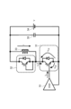
- FIG. 1 is a circuit diagram using a gate driver according to an embodiment of the present invention.
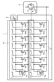
- FIG. 2 is a detailed configuration diagram of the IC in the gate driver.
- FIG. 3A is a detailed circuit diagram of the DAC in the gate driver.
- FIG. 3B is an equivalent circuit of the DAC.
- FIG. 3C is an explanatory diagram of the output of the DAC.
- FIG. 4 is a timing chart showing an example of active drive operation of the gate driver.
- FIG. 5A is a timing chart showing the single drive operation of the gate driver performed in the characteristic evaluation.
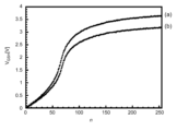
- FIG. 5B is a graph showing the characteristic evaluation results of the gate voltage V GSH .
- FIG. 5C is a graph showing the results of characteristic evaluation of gate current IG .
- FIG. 5A is a timing chart showing the single drive operation of the gate driver performed in the characteristic evaluation.
- FIG. 5B is a graph showing the characteristic evaluation results of the gate voltage V GSH .
- FIG. 5C is a graph showing
- FIG. 6A is a circuit configuration diagram of a double pulse test of a gate driver.
- FIG. 6B is a graph showing the evaluation results of single drive and active drive in the double pulse test.
- FIG. 7 is a circuit diagram showing a gate driver of a first modification.
- FIG. 8 is a circuit diagram showing a gate driver of a second modification.
- FIG. 1 is a circuit diagram using a gate driver according to an embodiment of the present invention.
- the gate driver 10 has its output terminal connected to the gate and emitter of the power transistor 20 in order to control the power transistor 20.
- the power transistor 20 is, for example, an IGBT (Insulated Gate Bipolar Transistor).
- IGBT Insulated Gate Bipolar Transistor
- the potential of the gate with respect to the emitter of the power transistor 20 will be referred to as gate voltage VGE
- gate current IG the current input to the gate
- the gate voltage VGE of the power transistor 20 changes in accordance with the output of the gate driver 10, and the power transistor 20 is controlled. Note that the gate current IG needs to exceed a predetermined value according to the specifications of the power transistor 20.
- the gate driver 10 has a half-bridge configuration, and has a two-stage configuration: an upper stage in the figure (high side) and a lower stage in the figure (low side). In the gate driver 10 having a half-bridge configuration, while one of the high side and low side is being controlled, the other does not operate.
- the gate driver 10 dynamically and variably controls the gate voltage V GE and gate current I G at a plurality of levels in response to a digital control signal input from the outside. By controlling the gate in this manner, the driving loss of the power transistor 20 can be reduced.
- the gate driver 10 is an example of a gate driving device, and a device that can variably control the gate voltage is sometimes referred to as a digital gate driver.
- dynamic variable control of the gate driver 10 at multiple levels is referred to as active control. Control of the gate driver 10 at one level (on/off) is referred to as single-step control or single control.
- the gate driver 10 constitutes a low side with a DAC (Digital Analog Converter) 1 and a MOSFET (Metal-Oxide-Semiconductor Field-Effect Transistor) 3 that constitute a high side.
- the two DACs 1 and 2, including their control circuits, are integrated circuits (ICs) and are implemented as an IC 11.
- the voltage of the gate to the source of the high-side MOSFET 3 is indicated as V GSH
- the voltage of the gate to the source of the low-side MOSFET 4 is indicated as V GSL .
- the gate voltages V GSH and V GSL of MOSFETs 3 and 4 are controlled by the DACs 1 and 2
- the gate voltages V GSH and V GSL output from the DACs 1 and 2 are used for switching the MOSFETs 3 and 4.
- a freewheeling diode is connected to the MOSFETs 3 and 4 between the drain and the source, with the source side serving as an anode, that is, connected in antiparallel to the MOSFETs 3 and 4.
- the output terminal of DAC1 is connected to the gate of MOSFET3.
- the DAC 1 is supplied with a DC voltage VDD3 from a power source 5. Further, one end of the DAC 1 connected to the negative electrode side of the power source 5 and the source of the MOSFET 3 are electrically connected.
- the DAC1 transforms the supplied voltage VDD3 according to a control signal input from the outside, and outputs it to the gate of the MOSFET3 at a desired level at a desired timing. Through such control of the DAC 1, the gate voltage V GSH is controlled and the MOSFET 3 operates.
- the MOSFET 3 has a source connected to the gate of the power transistor 20 and a drain connected to the emitter of the power transistor 20 via the power supply 7.
- the power supply 7 supplies a DC voltage V DD1 and is provided so that the gate of the power transistor 20 has a high potential with respect to the emitter, that is, the gate voltage V GE has a positive potential.
- the MOSFET 3 is controlled according to the gate voltage V GSH , and as a result, the gate voltage V GE of the power transistor 20 becomes a positive voltage obtained by stepping down the voltage V DD1 .
- the configuration on the low side is similar to the configuration on the high side.
- the output terminal of DAC2 is connected to the gate of MOSFET4.
- a DC voltage VDD4 is supplied to the DAC 2 from a power source 6. Further, one end of the DAC 2 connected to the negative electrode side of the power source 6 and the source of the MOSFET 4 are electrically connected.
- the DAC 2 transforms the supplied voltage V DD4 according to a control signal input from the outside, and outputs it to the gate of the MOSFET 4 at a desired level at a desired timing. Through such control of the DAC 2, the gate voltage V GSL is controlled and the MOSFET 4 operates.
- the MOSFET 4 has a drain connected to the gate of the power transistor 20, and a source connected to the emitter of the power transistor 20 via the power supply 8.
- the power supply 8 supplies a DC voltage V DD2 and is provided so that the emitter of the power transistor 20 has a higher potential than the gate, that is, the gate voltage V GE has a negative potential.
- the MOSFET 4 is controlled according to the gate voltage V GSL , and as a result, the gate voltage V GE of the power transistor 20 becomes a negative voltage obtained by lowering the voltage V DD2 .
- the gate voltages V GSH and V GSL of the MOSETs 3 and 4 are controlled according to the control of the DACs 1 and 2. Then, the gate voltage V GE and gate current I G of the power transistor 20 are controlled according to changes in the gate voltages V GSH and V GSL .
- the gate voltage V GE of the power transistor 20 is a positive voltage corresponding to the gate voltage V GSH of MOSET 3
- the gate voltage V GE of the power transistor 20 is the gate voltage V GE of MOSET 4. It becomes a negative voltage according to V GSL .
- the power transistor 20 is driven by such alternating high-side and low-side control.
- FIG. 2 is a detailed configuration diagram of the IC 11.
- the IC 11 is provided with a control circuit for the DACs 1 and 2.
- the power supplies 5 and 6 are shown on the right side of the DACs 1 and 2.
- the IC 11 includes shift registers 12 and 13, which are control circuits for the DACs 1 and 2, and an edge decoder 14.
- the control circuit including shift registers 12, 13 and edge decoder 14 may be implemented by any type of controller.
- the shift register 12 receives input of a serial signal and outputs a parallel signal.
- the shift register 13 receives input of a parallel signal and outputs a serial signal.
- the IC11 has input signals (IN) and enable signals (Enable) used for controlling DAC1 and 2, input signals (Scan IN) and clock signals (Scan CLK) used for scan design, and input signals from DAC1 and 2.
- a timing signal (Timing) indicating the change timing of the output (gate voltages V GSH , V GSL ) is input. Note that the scan design is implemented using the shift register 12 and the like, but a detailed explanation of its configuration will be omitted.
- the shift register 13 receives a timing signal (Timing) from the edge decoder 14 in addition to an input signal (IN) and an enable signal (Enable).
- the shift register 13 outputs 8-bit H_n PMOS and H_n NMOS control signals to the DAC1, and outputs 8-bit L_n PMOS and L_n NMOS control signals to the DAC2. Note that this output is updated at the change timing of the timing signal.
- the DACs 1 and 2 operate based on digital control signals using four 8-bit signals, and the gate voltages V GSH and V GSL , which are switching signals for the MOSFETs 3 and 4, are output.
- FIGS. 3A to 3C detailed configurations of the DACs 1 and 2 will be explained using FIGS. 3A to 3C.
- FIG. 3A is a detailed circuit configuration diagram of the DAC 1.
- FIG. 3B is an equivalent circuit of the DAC1.
- FIG. 3C is an explanatory diagram of the output of the DAC1.
- the DAC 1 includes a variable resistance section 15 in the upper part of the figure and a variable resistance part 16 in the lower part of the figure, so that the output of the DAC 1 can be variably controlled as shown in FIG. 3C.
- the details of the configuration of the DAC 1 will be described below.
- variable resistance section 15 is configured by connecting switching elements W P , 2W P , 4W P , 8W P , 16W P , 32W P , 64W P , and 128W P having resistance components in parallel. ing.
- One end of these switching elements WP is supplied with a voltage VDD3 from a power supply 5, and the other end is connected to the gate of MOSFET3.
- the number attached to the beginning of the switching element WP indicates the relative size of the area of the element. That is, the switching element 2WP has a resistance value that is 1/2 times as large as that of the switching element WP .
- the switching elements W P , 2W P , 4W P , 8W P , 16W P , 32W P , 64W P , and 128W P are controlled by the registers of H_n PMOS [0] to [7], respectively. As a result, the resistance value of the variable resistance section 15 can be changed in 256 levels (0 to 255: 8 bits).
- variable resistance section 16 is configured by connecting switching elements W N , 2W N , 4W N , 8W N , 16W N , 32W N , 64W N , and 128W N having resistance components in parallel.
- One end of these switching elements WN is connected to the gate of MOSFET3, and the other end is connected to the source of MOSFET3.
- the switching elements W N , 2W N , 4W N , 8W N , 16W N , 32W N , 64W N , and 128W N are controlled by registers of H_n NMOS [0] to [7], respectively.
- the resistance value of the variable resistance section 16 can be changed in 256 levels (0 to 255: 8 bits).
- the DAC 1 includes a variable resistance section 15 whose resistance value changes by being controlled by registers of H_n PMOS [0] to [7], and registers of H_n NMOS [0] to [7].
- This is equivalent to a configuration in which the variable resistance section 16 whose resistance value changes by being controlled is connected in series.
- a voltage V DD3 is supplied from the power supply 5 to the variable resistance sections 15 and 16. Further, the connection point between the variable resistance section 15 and the variable resistance section 16 is connected to the gate of the MOSFET 3, and the terminals of the variable resistance sections 15 and 16 connected to the negative electrode side of the power supply 5 are connected to the source of the MOSFET 3.
- the gate voltage V GSH of MOSFET 3 controlled by DAC 1 is shown.
- the gate voltage V GSH is determined by lowering the voltage V DD3 of the power supply 5 according to the resistance values of the variable resistance sections 15 and 16. Specifically, when the resistance value of the variable resistance section 15 is Rp and the resistance value of the variable resistance section 16 is RN , the gate voltage VGSH is ( RN /( RP +RN ) with respect to VDD3 . )).
- FIG. 4 is a timing chart showing an example of active drive operation of the gate driver 10. One period is configured by combining the cases where the IN signal input to the gate driver 10 is on (high side) and the case where it is off (low side).
- the gate voltage V GSH of the high-side MOSFET 3 is variably controlled at a plurality of levels, and the gate voltage V GSL of the low-side MOSFET 4 becomes zero.
- the gate voltage V GSH of the MOSFET 3 is controlled according to H_n PMOS [0] to [7], and the gate current I G and gate voltage V GE of the power transistor 20 are controlled.
- the gate voltage V GSH is set to a plurality of levels between 0V and V DD3 , and reaches V DD3 in the final interval t 5 .
- the gate voltage V GSL remains zero in the period t 1 to t 5 .
- the gate current IG increases or decreases in a positive range, but eventually becomes zero.
- the gate voltage V GE gradually increases and finally reaches a predetermined value V DD1 .
- the gate voltage V GSL of the low-side MOSFET 4 is variably controlled at a plurality of levels, and the high-side gate voltage V GSH becomes zero.
- the gate current I G of IGBT2 is controlled in a negative region, and the gate voltage V GE is controlled in a decreasing region. I can do it.
- the gate voltage V GSL of the low-side MOSFET 4 is set to a plurality of levels between 0V and V DD4 , and reaches V DD4 in the final interval t 10 .
- the gate voltage V GSH remains zero in the period t 6 to t 10 .
- the gate current I G increases or decreases in a negative range and eventually becomes zero.
- the gate voltage V GE gradually decreases to -V DD2 .
- the gate driver 10 can control the gate current I G and gate voltage V GE of the power transistor 20.
- FIG. 5A is a timing chart showing the single-step control operation of the gate driver 10 in characteristic evaluation.
- FIG. 5B is a graph showing the characteristics of the gate voltage V GSH .
- FIG. 5C is a graph showing the characteristics of gate current IG . This characteristic evaluation was performed in an environment where a 100 ⁇ F film capacitor was connected to the gate driver 10, and the evaluation results shown in FIGS. 5B and 5C were obtained by performing the single-step control shown in FIG. 5A.
- H_n PMOS changes from 0 to n (a predetermined value from 0 to 255)
- H_n NMOS changes from 255 to 60. Changed.
- H_n PMOS and H_n NMOS the gate voltage V GSH of MOSFET 3 and the gate current I G of power transistor 20 change.
- n in such control from 0 to 255
- characteristics of gate voltage V GSH and gate current I G as shown in FIGS. 5B and 5C were obtained.
- FIGS. 5B and 5C show measurement results under two conditions (a) and (b).
- (a) shows the characteristic results of the gate voltage V GSH and gate current I G according to changes in n when V DD1 and V DD2 are 15 V and V DD3 and V DD4 are 4 V.
- (b) shows the gate voltage V GSH and gate current I G as a function of the change in n when V DD1 is 15 V, V DD2 is 0 V, and V DD3 and V DD4 are 3.5 V, respectively. Characteristic results are shown.
- FIG. 5B a substantially linear correlation is shown in which the gate voltage V GSH increases by increasing n stepwise.
- FIG. 6A is a circuit configuration diagram of an evaluation environment for a double pulse test.
- FIG. 6B is a graph showing the drive performance of the gate driver 10 in a double pulse test.
- FIG. 6A shows a circuit diagram of a 600V/200A double pulse test.
- two power transistors 31 and 32 are connected in series.
- the gate of the power transistor 31 in the lower part of the figure receives input from the gate driver 10.
- An inductance 33 is connected in parallel to the power transistor 32 in the upper part of the figure.
- the power transistors 31 and 32 having a maximum collector-emitter voltage of 6500V and a maximum collector current of 1000A were used.
- V DD1 is 15V
- V DD2 is 0V
- V DD3 and V DD4 are 3.5V.
- a power source 34 is connected to both ends of the power transistors 31 and 32 connected in series, and a capacitor 35 is further provided in parallel with the power source 34.
- a voltage of 600V is supplied by the power supply 34, and a current of 200A flows through the inductance 33. In such an environment, a double pulse test was conducted by controlling the power transistor 31 using the gate driver 10.
- FIG. 6B is a diagram showing double pulse test results using the environment of FIG. 6A.
- the results of the double pulse test are shown; the overshoot current (I OVERSHOOOT ) of the power transistor 31 is shown on the X axis (horizontal axis), and the power loss (E LOSS ) of the power transistor 31 is shown on the Y axis (vertical axis). )It is shown.
- the circles indicate the correlation between overshoot current and power loss when n is changed from 94 to 255 when controlling the gate driver 10 using the single-step control shown in FIG. 5A. According to this figure, it can be understood that there is a trade-off relationship in which the smaller n is, the smaller the overshoot current is, and the larger n is, the smaller the power loss is.
- the asterisk indicates the result when the gate driver 10 is actively controlled.
- active control as shown in FIG. 4, the gate voltages V GSH and V GSL of MOSFET 3 are controlled to pass through an intermediate level while transitioning from off (low level) to on (high level). .
- the evaluation results shown in FIG. 6B were obtained by a different pattern of active control from that in FIG. 4.
- MOSFETs 3 and 4 are used as switches controlled by the DACs 1 and 2, but the present invention is not limited to this.
- Bipolar transistors may be used instead of MOSFETs. While MOSFETs are controlled according to gate voltage, bipolar transistors are controlled according to gate current. Therefore, by controlling the currents output from the DACs 1 and 2 at three or more levels including an intermediate level, the gate voltage of the power transistor 20 connected to the bipolar transistor can be variably and dynamically controlled.
- DACs 1 and 2 which are digital-to-analog converters, are used as control devices for controlling the switching elements, the present invention is not limited to this.
- a device capable of outputting signals of three or more levels, including one or more of a high level, a low level, and an intermediate level between the high level and the low level, according to an input control signal. may be used alternatively.
- the maximum value of the output current of the gate current IG of the power transistor 20 output from the gate driver 10 can be changed. Furthermore, by changing the voltages V DD3 and V DD4 of the power supplies 5 and 6 that supply power to the DACs 1 and 2 to power supplies with different voltages, the maximum value of the gate current I G output from the gate driver 10 can be changed. I can do it. Since the MOSFETs 3 and 4 and the power supplies 5 and 6 are modularized and easily replaced, the performance of the gate driver 10 can be changed by changing these parts.
- the gate driver 10 of this embodiment includes two DACs 1 and 2 and MOSFETs 3 and 4.
- the outputs from the DACs 1 and 2 include one or more of a high level, a low level, and an intermediate level between the high level and the low level, depending on the digital control signal input from the shift register 13. It is variably and dynamically controlled at the above levels.
- the MOSFETs 3 and 4 can dynamically control (active control) the gate voltage V GE and gate current I G of the power transistor 20 to be controlled at multiple levels according to the output levels from the DACs 1 and 2. can. As a result, as shown in FIG. 6B, it is possible to reduce both the overshoot current and power loss of the power transistor 20.
- control circuit for the DACs 1 and 2 is implemented by an IC 11 including a shift register 13.
- This IC 11 is provided with one control circuit (shift registers 12 and 13 and edge decoder 14) that outputs control signals to the two DACs 1 and 2.
- the IC 11 can be made smaller.
- the gate driver 10 has a half-bridge configuration including two sides, a high side and a low side, it can be operated in both turn-on control and turn-off control.
- the outputs of the DACs 1 and 2 are the gate voltages V GSH and V GSL of the MOSFETs 3 and 4, and such a configuration allows direct switching control of the MOSFETs 3 and 4.
- the switching control of MOSFETs 3 and 4 can also be performed indirectly by changing the voltage of the gates of MOSFETs 3 and 4 with respect to the ground. It can be implemented.
- the control accuracy of the MOSFETs 3 and 4 can be improved by changing directly rather than indirectly.
- FIG. 7 is a diagram showing a gate driver 10A of a first modification.
- the gate driver 10A shown in this figure is different from the gate driver 10 of the first embodiment shown in FIG.
- the power supply 8 that constitutes the output power is omitted.
- the DACs 1 and 2 are configured to be supplied with a predetermined voltage from the power source 7 instead of the power sources 5 and 6 by changing the voltage converters 41 and 42.
- the DACs 1 and 2 can be driven by transforming and supplying the voltage of the power supply 7 (second power supply) without providing the power supplies 5 and 6 (first power supply). be able to. Furthermore, even if one power supply 7 (second power supply) is provided for the two MOSFETs 3 and 4, the gate driver 10A can be configured. According to such a configuration, the number of power supplies in the gate driver 10A can be reduced and the configuration can be simplified.
- FIG. 8 is a diagram showing a gate driver 10B of a second modification.
- the gate driver 10B shown in this figure is different from the gate driver 10 of the first embodiment shown in FIG. is provided. With this configuration, the outputs from the DACs 1 and 2 can be smoothed, and as a result, the operation of the power transistor 20 operated by the gate driver 10B can be stabilized.
- the number of power supplies for the gate driver 10A can be reduced, and as shown in the second modification, the gate driver 10B can stabilize its operation by providing resistors 51 and 52. can be achieved.
- the gate driver 10 can take various modified examples.
Landscapes
- Power Conversion In General (AREA)
Priority Applications (5)
| Application Number | Priority Date | Filing Date | Title |
|---|---|---|---|
| PCT/JP2022/019327 WO2023209966A1 (ja) | 2022-04-28 | 2022-04-28 | ゲート駆動装置、および、ゲート駆動システム |
| CN202280095072.1A CN119054203A (zh) | 2022-04-28 | 2022-04-28 | 栅极驱动装置及栅极驱动系统 |
| US18/854,392 US20250253846A1 (en) | 2022-04-28 | 2022-04-28 | Gate drive device, and gate drive system |
| DE112022007109.5T DE112022007109T5 (de) | 2022-04-28 | 2022-04-28 | Gate-Ansteuervorrichtung und Gate-Ansteuersystem |
| JP2024517775A JP7833030B2 (ja) | 2022-04-28 | 2022-04-28 | ゲート駆動装置、および、ゲート駆動システム |
Applications Claiming Priority (1)
| Application Number | Priority Date | Filing Date | Title |
|---|---|---|---|
| PCT/JP2022/019327 WO2023209966A1 (ja) | 2022-04-28 | 2022-04-28 | ゲート駆動装置、および、ゲート駆動システム |
Publications (1)
| Publication Number | Publication Date |
|---|---|
| WO2023209966A1 true WO2023209966A1 (ja) | 2023-11-02 |
Family
ID=88518156
Family Applications (1)
| Application Number | Title | Priority Date | Filing Date |
|---|---|---|---|
| PCT/JP2022/019327 Ceased WO2023209966A1 (ja) | 2022-04-28 | 2022-04-28 | ゲート駆動装置、および、ゲート駆動システム |
Country Status (5)
| Country | Link |
|---|---|
| US (1) | US20250253846A1 (https=) |
| JP (1) | JP7833030B2 (https=) |
| CN (1) | CN119054203A (https=) |
| DE (1) | DE112022007109T5 (https=) |
| WO (1) | WO2023209966A1 (https=) |
Cited By (1)
| Publication number | Priority date | Publication date | Assignee | Title |
|---|---|---|---|---|
| CN119070598A (zh) * | 2024-11-06 | 2024-12-03 | 杭州飞仕得科技股份有限公司 | 驱动电源装置及自动化测试设备 |
Citations (4)
| Publication number | Priority date | Publication date | Assignee | Title |
|---|---|---|---|---|
| JP2005217774A (ja) * | 2004-01-29 | 2005-08-11 | Fujitsu Ten Ltd | スイッチング回路 |
| US20160134272A1 (en) * | 2014-11-07 | 2016-05-12 | Balanstring Technology, Llc | Switch Driver With a Low-Cost Cross-Conduction-Preventing Circuit |
| US20160329883A1 (en) * | 2015-05-07 | 2016-11-10 | Infineon Technologies Austria Ag | System and Method for a Switch Transistor Driver |
| JP2022048476A (ja) * | 2020-09-15 | 2022-03-28 | 株式会社東芝 | 駆動制御回路 |
Family Cites Families (1)
| Publication number | Priority date | Publication date | Assignee | Title |
|---|---|---|---|---|
| JP6346207B2 (ja) | 2016-01-28 | 2018-06-20 | 国立大学法人 東京大学 | ゲート駆動装置 |
-
2022
- 2022-04-28 WO PCT/JP2022/019327 patent/WO2023209966A1/ja not_active Ceased
- 2022-04-28 CN CN202280095072.1A patent/CN119054203A/zh active Pending
- 2022-04-28 DE DE112022007109.5T patent/DE112022007109T5/de active Pending
- 2022-04-28 US US18/854,392 patent/US20250253846A1/en active Pending
- 2022-04-28 JP JP2024517775A patent/JP7833030B2/ja active Active
Patent Citations (4)
| Publication number | Priority date | Publication date | Assignee | Title |
|---|---|---|---|---|
| JP2005217774A (ja) * | 2004-01-29 | 2005-08-11 | Fujitsu Ten Ltd | スイッチング回路 |
| US20160134272A1 (en) * | 2014-11-07 | 2016-05-12 | Balanstring Technology, Llc | Switch Driver With a Low-Cost Cross-Conduction-Preventing Circuit |
| US20160329883A1 (en) * | 2015-05-07 | 2016-11-10 | Infineon Technologies Austria Ag | System and Method for a Switch Transistor Driver |
| JP2022048476A (ja) * | 2020-09-15 | 2022-03-28 | 株式会社東芝 | 駆動制御回路 |
Cited By (1)
| Publication number | Priority date | Publication date | Assignee | Title |
|---|---|---|---|---|
| CN119070598A (zh) * | 2024-11-06 | 2024-12-03 | 杭州飞仕得科技股份有限公司 | 驱动电源装置及自动化测试设备 |
Also Published As
| Publication number | Publication date |
|---|---|
| JPWO2023209966A1 (https=) | 2023-11-02 |
| JP7833030B2 (ja) | 2026-03-18 |
| US20250253846A1 (en) | 2025-08-07 |
| CN119054203A (zh) | 2024-11-29 |
| DE112022007109T5 (de) | 2025-02-20 |
Similar Documents
| Publication | Publication Date | Title |
|---|---|---|
| US10554202B2 (en) | Gate driver | |
| KR101050696B1 (ko) | 전압 구동형 소자를 구동시키는 구동 장치 | |
| JP6934087B2 (ja) | ゲート駆動回路 | |
| JP2023062427A (ja) | スイッチング回路、dc/dcコンバータおよびその制御回路 | |
| JP2020124092A (ja) | スイッチング回路 | |
| JP2026040706A (ja) | ブリッジ回路の駆動回路、それを用いたモータ駆動装置、電子機器 | |
| JP7833030B2 (ja) | ゲート駆動装置、および、ゲート駆動システム | |
| JP2020195213A (ja) | スイッチングトランジスタの駆動回路 | |
| US6813169B2 (en) | Inverter device capable of reducing through current | |
| CN111869068B (zh) | 开关装置以及开关装置的控制方法 | |
| CN119210416B (zh) | 一种SiC MOSFET驱动电路及其控制方法 | |
| CN121217117A (zh) | 栅极驱动器和开关装置 | |
| JP2020096444A (ja) | スイッチング回路 | |
| US20250015798A1 (en) | Gate driver circuit | |
| JP2019154134A (ja) | ゲート駆動装置 | |
| KR20190108785A (ko) | 전원 변환기, 스위칭 소자 구동 장치 및 부하 구동 장치 | |
| CN117879313A (zh) | 一种优化开关过冲及损耗的多阶段igbt驱动电路及驱动方法 | |
| US20250105840A1 (en) | Gate driver circuit, motor drive device using same, and electronic device | |
| WO2024154283A1 (ja) | ゲートドライブ回路及び半導体装置 | |
| US20230179199A1 (en) | Drive circuit | |
| US20260095176A1 (en) | Gate Driver Circuit, Motor Driving Device Using the Same, and Electronic Apparatus | |
| JP2026000286A (ja) | アクティブゲート駆動回路およびその動作方法 | |
| JP2026046705A (ja) | インバータ装置 | |
| WO2024257615A1 (ja) | スイッチング駆動装置 | |
| JP2024076048A (ja) | 時間検出回路 |
Legal Events
| Date | Code | Title | Description |
|---|---|---|---|
| 121 | Ep: the epo has been informed by wipo that ep was designated in this application |
Ref document number: 22940240 Country of ref document: EP Kind code of ref document: A1 |
|
| ENP | Entry into the national phase |
Ref document number: 2024517775 Country of ref document: JP Kind code of ref document: A |
|
| WWE | Wipo information: entry into national phase |
Ref document number: 18854392 Country of ref document: US |
|
| WWE | Wipo information: entry into national phase |
Ref document number: 202280095072.1 Country of ref document: CN |
|
| WWE | Wipo information: entry into national phase |
Ref document number: 112022007109 Country of ref document: DE |
|
| WWP | Wipo information: published in national office |
Ref document number: 112022007109 Country of ref document: DE |
|
| 122 | Ep: pct application non-entry in european phase |
Ref document number: 22940240 Country of ref document: EP Kind code of ref document: A1 |
|
| WWP | Wipo information: published in national office |
Ref document number: 18854392 Country of ref document: US |