WO2023203614A1 - レーザ加工装置、レーザ加工方法、レーザ加工プログラム、記録媒体、半導体チップ製造方法および半導体チップ - Google Patents
レーザ加工装置、レーザ加工方法、レーザ加工プログラム、記録媒体、半導体チップ製造方法および半導体チップ Download PDFInfo
- Publication number
- WO2023203614A1 WO2023203614A1 PCT/JP2022/018064 JP2022018064W WO2023203614A1 WO 2023203614 A1 WO2023203614 A1 WO 2023203614A1 JP 2022018064 W JP2022018064 W JP 2022018064W WO 2023203614 A1 WO2023203614 A1 WO 2023203614A1
- Authority
- WO
- WIPO (PCT)
- Prior art keywords
- processing
- line
- irradiation position
- laser irradiation
- laser
- Prior art date
- Legal status (The legal status is an assumption and is not a legal conclusion. Google has not performed a legal analysis and makes no representation as to the accuracy of the status listed.)
- Ceased
Links
Images


















Classifications
-
- B—PERFORMING OPERATIONS; TRANSPORTING
- B23—MACHINE TOOLS; METAL-WORKING NOT OTHERWISE PROVIDED FOR
- B23K—SOLDERING OR UNSOLDERING; WELDING; CLADDING OR PLATING BY SOLDERING OR WELDING; CUTTING BY APPLYING HEAT LOCALLY, e.g. FLAME CUTTING; WORKING BY LASER BEAM
- B23K26/00—Working by laser beam, e.g. welding, cutting or boring
- B23K26/08—Devices involving relative movement between laser beam and workpiece
- B23K26/0869—Devices involving movement of the laser head in at least one axial direction
- B23K26/0876—Devices involving movement of the laser head in at least one axial direction in at least two axial directions
-
- H—ELECTRICITY
- H10—SEMICONDUCTOR DEVICES; ELECTRIC SOLID-STATE DEVICES NOT OTHERWISE PROVIDED FOR
- H10P—GENERIC PROCESSES OR APPARATUS FOR THE MANUFACTURE OR TREATMENT OF DEVICES COVERED BY CLASS H10
- H10P72/00—Handling or holding of wafers, substrates or devices during manufacture or treatment thereof
- H10P72/50—Handling or holding of wafers, substrates or devices during manufacture or treatment thereof for positioning, orientation or alignment
- H10P72/53—Handling or holding of wafers, substrates or devices during manufacture or treatment thereof for positioning, orientation or alignment using optical controlling means
-
- B—PERFORMING OPERATIONS; TRANSPORTING
- B23—MACHINE TOOLS; METAL-WORKING NOT OTHERWISE PROVIDED FOR
- B23K—SOLDERING OR UNSOLDERING; WELDING; CLADDING OR PLATING BY SOLDERING OR WELDING; CUTTING BY APPLYING HEAT LOCALLY, e.g. FLAME CUTTING; WORKING BY LASER BEAM
- B23K26/00—Working by laser beam, e.g. welding, cutting or boring
-
- B—PERFORMING OPERATIONS; TRANSPORTING
- B23—MACHINE TOOLS; METAL-WORKING NOT OTHERWISE PROVIDED FOR
- B23K—SOLDERING OR UNSOLDERING; WELDING; CLADDING OR PLATING BY SOLDERING OR WELDING; CUTTING BY APPLYING HEAT LOCALLY, e.g. FLAME CUTTING; WORKING BY LASER BEAM
- B23K26/00—Working by laser beam, e.g. welding, cutting or boring
- B23K26/02—Positioning or observing the workpiece, e.g. with respect to the point of impact; Aligning, aiming or focusing the laser beam
- B23K26/03—Observing, e.g. monitoring, the workpiece
-
- B—PERFORMING OPERATIONS; TRANSPORTING
- B23—MACHINE TOOLS; METAL-WORKING NOT OTHERWISE PROVIDED FOR
- B23K—SOLDERING OR UNSOLDERING; WELDING; CLADDING OR PLATING BY SOLDERING OR WELDING; CUTTING BY APPLYING HEAT LOCALLY, e.g. FLAME CUTTING; WORKING BY LASER BEAM
- B23K26/00—Working by laser beam, e.g. welding, cutting or boring
- B23K26/02—Positioning or observing the workpiece, e.g. with respect to the point of impact; Aligning, aiming or focusing the laser beam
- B23K26/03—Observing, e.g. monitoring, the workpiece
- B23K26/032—Observing, e.g. monitoring, the workpiece using optical means
-
- B—PERFORMING OPERATIONS; TRANSPORTING
- B23—MACHINE TOOLS; METAL-WORKING NOT OTHERWISE PROVIDED FOR
- B23K—SOLDERING OR UNSOLDERING; WELDING; CLADDING OR PLATING BY SOLDERING OR WELDING; CUTTING BY APPLYING HEAT LOCALLY, e.g. FLAME CUTTING; WORKING BY LASER BEAM
- B23K26/00—Working by laser beam, e.g. welding, cutting or boring
- B23K26/02—Positioning or observing the workpiece, e.g. with respect to the point of impact; Aligning, aiming or focusing the laser beam
- B23K26/04—Automatically aligning, aiming or focusing the laser beam, e.g. using the back-scattered light
-
- B—PERFORMING OPERATIONS; TRANSPORTING
- B23—MACHINE TOOLS; METAL-WORKING NOT OTHERWISE PROVIDED FOR
- B23K—SOLDERING OR UNSOLDERING; WELDING; CLADDING OR PLATING BY SOLDERING OR WELDING; CUTTING BY APPLYING HEAT LOCALLY, e.g. FLAME CUTTING; WORKING BY LASER BEAM
- B23K26/00—Working by laser beam, e.g. welding, cutting or boring
- B23K26/08—Devices involving relative movement between laser beam and workpiece
- B23K26/082—Scanning systems, i.e. devices involving movement of the laser beam relative to the laser head
-
- B—PERFORMING OPERATIONS; TRANSPORTING
- B23—MACHINE TOOLS; METAL-WORKING NOT OTHERWISE PROVIDED FOR
- B23K—SOLDERING OR UNSOLDERING; WELDING; CLADDING OR PLATING BY SOLDERING OR WELDING; CUTTING BY APPLYING HEAT LOCALLY, e.g. FLAME CUTTING; WORKING BY LASER BEAM
- B23K26/00—Working by laser beam, e.g. welding, cutting or boring
- B23K26/08—Devices involving relative movement between laser beam and workpiece
- B23K26/083—Devices involving movement of the workpiece in at least one axial direction
- B23K26/0853—Devices involving movement of the workpiece in at least two axial directions, e.g. in a plane
-
- B—PERFORMING OPERATIONS; TRANSPORTING
- B23—MACHINE TOOLS; METAL-WORKING NOT OTHERWISE PROVIDED FOR
- B23K—SOLDERING OR UNSOLDERING; WELDING; CLADDING OR PLATING BY SOLDERING OR WELDING; CUTTING BY APPLYING HEAT LOCALLY, e.g. FLAME CUTTING; WORKING BY LASER BEAM
- B23K26/00—Working by laser beam, e.g. welding, cutting or boring
- B23K26/08—Devices involving relative movement between laser beam and workpiece
- B23K26/0869—Devices involving movement of the laser head in at least one axial direction
-
- B—PERFORMING OPERATIONS; TRANSPORTING
- B23—MACHINE TOOLS; METAL-WORKING NOT OTHERWISE PROVIDED FOR
- B23K—SOLDERING OR UNSOLDERING; WELDING; CLADDING OR PLATING BY SOLDERING OR WELDING; CUTTING BY APPLYING HEAT LOCALLY, e.g. FLAME CUTTING; WORKING BY LASER BEAM
- B23K26/00—Working by laser beam, e.g. welding, cutting or boring
- B23K26/36—Removing material
- B23K26/38—Removing material by boring or cutting
-
- H—ELECTRICITY
- H10—SEMICONDUCTOR DEVICES; ELECTRIC SOLID-STATE DEVICES NOT OTHERWISE PROVIDED FOR
- H10P—GENERIC PROCESSES OR APPARATUS FOR THE MANUFACTURE OR TREATMENT OF DEVICES COVERED BY CLASS H10
- H10P72/00—Handling or holding of wafers, substrates or devices during manufacture or treatment thereof
- H10P72/04—Apparatus for manufacture or treatment
- H10P72/0428—Apparatus for mechanical treatment or grinding or cutting
-
- H—ELECTRICITY
- H10—SEMICONDUCTOR DEVICES; ELECTRIC SOLID-STATE DEVICES NOT OTHERWISE PROVIDED FOR
- H10P—GENERIC PROCESSES OR APPARATUS FOR THE MANUFACTURE OR TREATMENT OF DEVICES COVERED BY CLASS H10
- H10P72/00—Handling or holding of wafers, substrates or devices during manufacture or treatment thereof
- H10P72/70—Handling or holding of wafers, substrates or devices during manufacture or treatment thereof for supporting or gripping
- H10P72/74—Handling or holding of wafers, substrates or devices during manufacture or treatment thereof for supporting or gripping using temporarily an auxiliary support
- H10P72/7416—Handling or holding of wafers, substrates or devices during manufacture or treatment thereof for supporting or gripping using temporarily an auxiliary support used during dicing or grinding
- H10P72/742—Handling or holding of wafers, substrates or devices during manufacture or treatment thereof for supporting or gripping using temporarily an auxiliary support used during dicing or grinding involving stretching of the auxiliary support post dicing
-
- B—PERFORMING OPERATIONS; TRANSPORTING
- B23—MACHINE TOOLS; METAL-WORKING NOT OTHERWISE PROVIDED FOR
- B23K—SOLDERING OR UNSOLDERING; WELDING; CLADDING OR PLATING BY SOLDERING OR WELDING; CUTTING BY APPLYING HEAT LOCALLY, e.g. FLAME CUTTING; WORKING BY LASER BEAM
- B23K2101/00—Articles made by soldering, welding or cutting
- B23K2101/36—Electric or electronic devices
- B23K2101/40—Semiconductor devices
-
- H—ELECTRICITY
- H10—SEMICONDUCTOR DEVICES; ELECTRIC SOLID-STATE DEVICES NOT OTHERWISE PROVIDED FOR
- H10P—GENERIC PROCESSES OR APPARATUS FOR THE MANUFACTURE OR TREATMENT OF DEVICES COVERED BY CLASS H10
- H10P54/00—Cutting or separating of wafers, substrates or parts of devices
Definitions
- the present invention relates to a technique for processing a processing line provided on a workpiece by irradiating the processing line with a laser beam.
- Patent Documents 1 to 3 disclose a laser processing technology that processes the planned dividing line by irradiating the planned dividing line provided on the semiconductor substrate with a laser beam and moving the laser beam relatively to the semiconductor substrate.
- Patent Document 1 in this laser processing technology, by reciprocating the laser beam while changing the scheduled division lines on which the laser beam is irradiated on the outbound and return passes, the laser beam is reciprocated, so that multiple division lines are Machining is performed. At this time, the position of the laser beam is adjusted according to the result of an alignment process that recognizes the position of the planned dividing line based on the image obtained by capturing a predetermined location on the semiconductor substrate. It is possible to irradiate accurately (Patent Document 2).
- Patent Document 3 by processing the planned dividing line with a laser beam, the width of the planned dividing line expands, and the position of the unprocessed planned dividing line moves in the feeding direction perpendicular to the processing direction. It may shift. In order to deal with such a positional shift of the scheduled dividing line, it is appropriate to image the semiconductor substrate as appropriate.
- Patent No. 5804716 Japanese Patent Application Publication No. 5554593 Japanese Patent Application Publication No. 5037082
- the laser processing technology described above requires efficient imaging of the workpiece (semiconductor substrate) in order to recognize the effects of laser beam irradiation on the processing line (dividing line). .
- This invention has been made in view of the above-mentioned problems, and provides a technique that enables efficient imaging of a workpiece in a laser processing technology that processes a processing line by irradiating a laser beam onto the processing line. With the goal.
- a laser processing apparatus includes a support member that supports a workpiece having a plurality of processing lines parallel to each other so that the processing lines are parallel to a predetermined processing direction, and a laser beam at a predetermined laser irradiation position.
- a processing head that irradiates the laser beam
- a processing axis drive unit that moves the laser irradiation position relative to the workpiece in the processing direction by driving at least one of the support member and the processing head in the processing direction
- a processing axis that moves the laser irradiation position relative to the workpiece in the processing direction.
- a control unit that executes line processing processing that processes the processing line by moving the laser irradiation position along the processing line using the drive unit and irradiating the laser beam at the laser irradiation position with the processing head, and a control unit that processes the processing line by moving the laser irradiation position along the processing line and controlling the laser irradiation position as the processing target.
- an imaging unit that images a predetermined imaging range that moves relative to the object to be processed integrally with the laser irradiation position as the object moves relative to the object; An image of a portion of the workpiece that overlaps with the imaging range is acquired by imaging an imaging range that moves relative to the workpiece during execution of processing.
- the laser processing method includes the steps of supporting a workpiece having a plurality of processing lines parallel to each other by a support member so that the processing lines are parallel to a predetermined processing direction, and positioning a predetermined laser irradiation position.
- the laser irradiation position is processed by a processing axis drive unit that moves the laser irradiation position relative to the workpiece in the processing direction by driving at least one of the processing head and the support member that irradiates the laser beam in the processing direction.
- a process of performing line processing processing in which the processing line is processed by irradiating the laser beam at the laser irradiation position with the processing head while moving along the line, and the process of moving the laser irradiation position relative to the workpiece.
- the imaging unit which captures a predetermined imaging range that moves integrally with the laser irradiation position relative to the workpiece, moves relative to the workpiece during line processing. and acquiring an image of a portion of the workpiece that overlaps with the imaging range by imaging the imaging range.
- line processing processing is performed in which the processing line is processed by irradiating the laser beam at the laser irradiation position while moving the laser irradiation position along the processing line.
- an image of a portion of the workpiece that overlaps with the imaging range is acquired by imaging an imaging range that moves relative to the workpiece.
- the execution period of the line machining process is effectively utilized for imaging the workpiece.
- the laser processing device may be configured such that the imaging unit images an imaging range provided on the downstream side in the direction in which the laser irradiation position moves with respect to the processing line in the line processing process.
- the imaging unit images an imaging range provided on the downstream side in the direction in which the laser irradiation position moves with respect to the processing line in the line processing process.
- the laser processing device may be configured such that the imaging unit performs imaging of the imaging range multiple times during a period in which the line processing process is performed once. With this configuration, a plurality of images of the workpiece can be acquired by effectively utilizing the execution period of the line processing process.
- the invention further includes a feed shaft drive unit that moves the laser irradiation position relative to the workpiece in the feed direction by driving at least one of the support member and the processing head in the feed direction perpendicular to the processing direction, By moving the laser irradiation position on the workpiece in the feed direction by the feed axis drive unit, the processing line targeted for line processing among the multiple processing lines is changed, and the control unit changes the processing line in the processing direction.
- a first line processing process that processes the first processing line out of a plurality of processing lines by moving the laser irradiation position to the first side, and a second line processing process that processes the first processing line among the plurality of processing lines, and a second line processing process that moves the laser irradiation position to the first side.
- the machining axis drive section is configured to control the laser irradiation that has passed through the first machining line to the first side in the machining direction.
- a reversal drive is executed to bring the laser irradiation position to the second processing line
- the feed axis drive unit is a process from a first virtual straight line extending in the machining direction along the first machining line to the outside of the first machining line to the outside of the second machining line along the second machining line.
- the controller executes a continuous feed drive that continuously moves the laser irradiation position in the feed direction until it reaches a second virtual straight line extending in the direction, and the control unit stops the laser irradiation position by driving the processing axis drive unit in reverse.
- the processing axis drive unit starts continuous feeding drive before the machine starts moving, and after the processing axis drive unit stops the laser irradiation position by reverse driving, the processing axis drive unit ends continuous feeding drive.
- a laser processing device that controls the feed shaft drive unit to cause the feed shaft drive unit to move the laser irradiation position in the feed direction before and after the time when the movement of the laser irradiation position in the processing direction stops for reversal driving. may be configured.
- a processing shaft drive unit moves the laser irradiation position relative to the workpiece in the processing direction
- a feed shaft drive unit moves the laser irradiation position relative to the workpiece in the feed direction.
- a first line machining process for machining the first machining line and a second line machining process for machining the second machining line are performed using the above.
- the processing axis is driven to direct the laser irradiation position that has passed through the first processing line to the second processing line.
- the unit and the feed shaft drive unit perform the following operations.
- the processing axis drive section decelerates and stops the laser irradiation position that has passed through the first processing line to the first side toward the first side, and then moves the laser irradiation position toward the second side.
- a reversal drive is executed in which the laser irradiation position reaches the second processing line.
- the feed shaft drive section moves from a first imaginary straight line extending in the processing direction along the first processing line to the outside of the first processing line to a second imaginary straight line along the second processing line.
- the laser irradiation position is moved in the feeding direction onto a second virtual straight line extending in the processing direction to the outside of the processing line.
- the feed shaft drive unit executes a continuous feed drive that continuously moves the laser irradiation position in the feed direction from the first virtual straight line to the second virtual straight line. Then, the control unit causes the feed axis drive unit to start continuous feed drive before the processing axis drive unit stops the laser irradiation position by reverse drive, and the process axis drive unit stops the laser irradiation position by reverse drive.
- the processing axis drive unit and the feed axis drive unit are controlled so that the feed axis drive unit ends the continuous feed drive after that, and the feed continues before and after the point in time when the movement of the laser irradiation position in the processing direction stops for reversal drive.
- the shaft drive unit moves the laser irradiation position in the feeding direction.
- both the period of decelerating the laser irradiation position to the first side in the processing direction and the period of accelerating the laser irradiation position to the second side of the processing direction are both in the feeding direction of the laser irradiation position. It is effectively used for transportation. As a result, it is possible to suppress the influence of the switching period for switching the moving direction of the laser beam on the time required to complete processing of the workpiece. Moreover, as mentioned above, since the execution period of the line processing process is effectively used for imaging the workpiece, the time required to change the processing line that is the target of the line processing process can be reduced, and the time taken to image the workpiece can be reduced. can be carried out efficiently, and the processing on the workpiece can be completed quickly.
- the laser processing apparatus may be configured such that the imaging unit images an imaging range that includes at least the processing line during execution of the line processing process. In the image obtained by such imaging, a portion corresponding to the processing line appears extending in the processing direction due to the contrast between both sides of the processing line in the feeding direction and the processing line. Therefore, the influence of laser processing on the position of the processing line in the feed direction can be accurately recognized based on the position of the part in the feed direction.
- the laser processing apparatus may be configured such that the center of the imaging range of the imaging unit and the focus of the laser light irradiated to the laser irradiation position are aligned in the processing direction. With this configuration, the state immediately before being irradiated with laser light can be accurately captured by an image of the imaging range.
- the imaging unit detects that an unprocessed portion of the one target line that has not been processed by laser beam irradiation intersects with the imaging range.
- the laser processing apparatus may be configured to acquire images by imaging the whole period in which the camera continues to expose the light throughout the period. With this configuration, it is possible to obtain information in which the luminance of images in the imaging range is accumulated in the processing direction.
- Lc T0 ⁇ L0/Tc
- control unit may configure the laser processing apparatus to determine whether or not the laser irradiation position with respect to the processing line is appropriate based on images acquired by imaging during the entire period. With this configuration, it is possible to confirm whether the laser irradiation position is appropriate.
- the control unit may configure the laser processing apparatus to determine whether or not the laser irradiation position is appropriate for the processing line based on the central part of the image excluding both ends in the orthogonal direction orthogonal to the processing direction. good. With this configuration, the suitability of the laser irradiation position can be confirmed by removing unnecessary information appearing at both ends of the image in the orthogonal direction.
- the control unit determines whether the laser irradiation position has shifted in an orthogonal direction to one target line.
- the laser processing apparatus may be configured to acquire the amount of positional deviation and correct the laser irradiation position in the orthogonal direction based on the amount of positional deviation when line processing is performed after one target line. With this configuration, it is possible to correct the positional deviation of the laser irradiation position and appropriately execute the line processing process.
- control unit may configure the laser processing apparatus so that, when the inclination of the locus of the laser irradiation position with respect to one target line is confirmed based on the image, the control unit executes alignment to correct the inclination.
- the control unit executes alignment to correct the inclination.
- the semiconductor chip manufacturing method includes the steps of processing a semiconductor substrate on which a plurality of semiconductor chips separated by processing lines are arranged, by the above-described laser processing method, and bonding the semiconductor substrate processed by the laser processing method. and separating each of the plurality of semiconductor chips by expanding the tape held by force.
- the semiconductor chip according to the present invention includes a step of processing a semiconductor substrate on which a plurality of semiconductor chips separated by processing lines are arranged, by the above-mentioned laser processing method, and a process of processing the semiconductor substrate processed by the laser processing method using adhesive force. It is manufactured by a process of separating each of a plurality of semiconductor chips by expanding a holding tape.
- a laser processing program causes a computer to execute the above laser processing method.
- a recording medium records the above-mentioned laser processing program so as to be readable by a computer.
- FIG. 1 is a front view schematically showing an example of a laser processing apparatus according to the present invention.
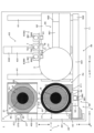
- 2 is a plan view schematically showing the laser processing apparatus of FIG. 1.
- FIG. FIG. 2 is a block diagram showing the electrical configuration of the laser processing apparatus of FIG. 1.
- FIG. 2 is a flowchart illustrating an example of a method for producing a laser-processed substrate that has been laser-processed. The flowchart which shows an example of taking out a ring frame.
- 5 is a flowchart showing an example of transferring a ring frame.
- FIG. 7 is a plan view schematically showing an example of operations performed according to the flowcharts of FIGS. 5 and 6.
- FIG. 7 is a plan view schematically showing an example of operations performed according to the flowcharts of FIGS. 5 and 6.
- FIG. 7 is a plan view schematically showing an example of operations performed according to the flowcharts of FIGS. 5 and 6.
- FIG. 7 is a plan view schematically showing an example of operations performed according to the flowcharts of FIGS. 5 and 6.
- FIG. 7 is a plan view schematically showing an example of operations performed according to the flowcharts of FIGS. 5 and 6.
- FIG. 3 is a plan view schematically showing an example of an operation performed in ring frame alignment.
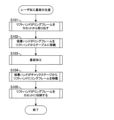
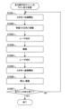
- FIG. 1 is a flowchart showing an example of substrate processing.
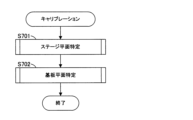
- FIG. 12 is a plan view schematically showing an example of operations performed according to the flowchart of FIG. 11; 5 is a flowchart showing an example of calibration.
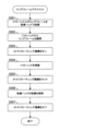
- 13A is a flowchart showing an example of stage plane identification performed in the calibration of FIG. 13A.
- 13A is a flowchart showing an example of substrate plane identification performed in the calibration of FIG. 13A.
- 2 is a flowchart showing the basic steps of line processing for each scheduled division line.
- 15 is a diagram schematically showing a first example of operations performed according to the flowchart of FIG. 14.
- FIG. 15 is a diagram schematically showing a second example of operations performed according to the flowchart of FIG. 14.
- FIG. 15 is a diagram schematically showing a third example of operations performed according to the flowchart of FIG. 14.
- FIG. 15 is a diagram schematically showing a fourth example of operations performed according to the flowchart of FIG. 14.
- FIG. 15 is a diagram schematically showing a fifth example of operations performed according to the flowchart of FIG. 14.
- FIG. 15 is a diagram schematically showing a sixth example of operations performed according to the flowchart of FIG. 14.
- FIG. 15 is a diagram schematically showing a seventh example of operations performed according to the flowchart of FIG. 14.
- FIG. 12 is a flowchart showing a first application example of line processing processing for each scheduled division line.
- FIG. 17 is a diagram schematically showing an example of operations performed according to the flowchart of FIG.
- FIG. 19 is a diagram schematically showing a first example of operations performed according to the flowchart of FIG. 18.
- FIG. 19 is a diagram schematically showing a second example of operations performed according to the flowchart of FIG. 18.
- FIG. 18 is a diagram schematically showing an example of an image of a semiconductor substrate acquired in step S1008 of FIG. 16 or step S1104 of FIG. 18.
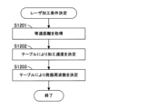
- FIG. 5 is a flowchart illustrating an example of a method for determining laser processing conditions in line processing.
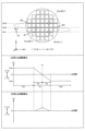
- FIG. 3 is a diagram showing parameters related to determining laser processing conditions. A diagram showing the temporal influence of laser processing conditions.
- FIG. 22 is a diagram showing an example of a table referred to in determining the laser processing conditions in FIG. 21.
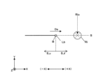
- FIG. FIG. 7 is a plan view schematically showing the positional relationship between the laser irradiation position and the imaging range in a detailed operation of imaging the imaging range.
- FIG. 3 is a plan view schematically showing an imaging target in a detailed operation of imaging an imaging range.
- 5 is a flowchart showing an example of camera exposure control.
- FIG. 3 is a diagram schematically showing information that can be obtained from a panning image captured by a panning operation.
- 5 is a flowchart illustrating an example of image determination performed on a continuous shot image.
- FIG. 28 is a diagram schematically showing a mask used in the image determination of FIG. 27;
- FIG. 1 is a front view schematically showing an example of a laser processing apparatus according to the present invention
- FIG. 2 is a plan view schematically showing the laser processing apparatus of FIG. 1.
- the X direction which is a horizontal direction
- the Y direction which is a horizontal direction perpendicular to the X direction
- the Z direction which is a vertical direction
- the (+X) side in the X direction (the right side of the paper in Figure 2) and the (-X) side opposite to the (+X) side in the X direction (the left side in the paper in Figure 2)
- (+Y) side upper side of the paper in FIG. 2) and ( ⁇ Y) side (lower side of the paper in FIG. 2), which is opposite to the (+Y) side in the Y direction, are shown as appropriate.
- the laser processing apparatus 1 processes the semiconductor substrate W (workpiece) by irradiating the semiconductor substrate W (workpiece) with laser light.
- This semiconductor substrate W is held by a ring frame Fr via a tape E.
- Tape E is a dicing tape or bonding tape, and the surface (upper surface) of tape E has adhesiveness.
- the ring frame Fr has an outer shape in which a part of a regular octagon is cut out to provide a slit Fs, and a circular opening Fo is provided in the center of the ring frame Fr.
- the surface of the tape E faces the ring frame Fr from below so as to overlap the entire opening Fo, and the peripheral edge of the surface of the tape E is adhered to the bottom surface of the ring frame Fr by adhesive force.
- the semiconductor substrate W is attached to the surface of the tape E by adhesive force. In this manner, the semiconductor substrate W is transported within the laser processing apparatus 1 while being held by the ring frame Fr via the tape E.
- the semiconductor substrate W has a front surface and a back surface opposite to the front surface, and while an electronic circuit is formed on the front surface of the semiconductor substrate W, the back surface of the semiconductor substrate W is flat.
- the semiconductor substrate W is attached to the surface of the tape E with the front surface facing downward. That is, the semiconductor substrate W is held with the back surface of the semiconductor substrate W facing upward.
- the laser processing apparatus 1 includes a substrate accommodating section 2 that accommodates a semiconductor substrate W, and a chuck stage 3 (support member) that holds the semiconductor substrate W taken out from the substrate accommodating section 2.
- the laser processing apparatus 1 includes a flat base plate 11 , and the substrate accommodating section 2 and the chuck stage 3 are supported by the base plate 11 .
- the chuck stage 3 In the X direction, the chuck stage 3 is arranged on the (+X) side of the substrate accommodating section 2, and in the Y direction, the chuck stage 3 is arranged on the (-Y) side of the substrate accommodating section 2.
- the space on the (-X) side of the chuck stage 3 in the X direction and on the (-Y) side of the substrate storage section 2 in the Y direction becomes the substrate transfer area Aw.
- the substrate storage section 2 has a substrate storage cassette 21.
- the substrate storage cassette 21 has a pair of side walls 22 provided on both sides in the X direction, and an opening 23 provided between the side walls 22. side).
- the pair of side walls 22 are flat plates provided perpendicularly to the X direction, and face each other in the X direction.
- a support protrusion 24 is provided inside each of the pair of side walls 22 . In this way, a pair of support protrusions 24 facing each other in the X direction are provided at the same height. Then, the ring frame Fr that holds the semiconductor substrate W can be inserted into the upper side of the pair of support protrusions 24 from the (-Y) side through the opening 23.
- Both ends of the ring frame Fr inserted in the X direction are supported from below by a pair of support protrusions 24. That is, the upper side of the pair of support protrusions 24 functions as the slot 25 that accommodates the ring frame Fr, and the ring frame Fr inserted into the slot 25 from the (-Y) side through the opening 23 corresponds to the slot 25. It is supported by a pair of support protrusions 24. Therefore, by inserting the ring frame Fr into the slot 25 of the substrate storage cassette 21, the semiconductor substrate W supported by the ring frame Fr can be stored in the substrate storage cassette 21, and the ring frame Fr can be inserted from the slot 25 of the substrate storage cassette 21. By pulling it out, the semiconductor substrate W can be taken out from the substrate storage cassette 21.
- the substrate storage section 2 includes a Z-axis slider 26 that supports the substrate storage cassette 21, and a Z-axis drive mechanism 27 that drives the Z-axis slider 26 in the Z direction.
- the Z-axis drive mechanism 27 is a single-axis robot attached to the base plate 11, and includes a Z-axis drive transmission section 271 that supports the Z-axis slider 26 movably in the Z direction, and a Z-axis drive transmission section 271 supported by the Z-axis drive transmission section 271. It has a Z-axis cassette motor 272 that drives the shaft slider 26 in the Z direction.
- the Z-axis drive transmission section 271 has a ball screw driven by a Z-axis cassette motor 272, and the Z-axis slider 26 is attached to a nut of the ball screw.
- the specific configuration of the Z-axis drive mechanism 27 is not limited to this example, and may be a linear motor, for example.
- the Z-axis drive mechanism 27 drives the Z-axis slider 26 supported by the Z-axis drive transmission section 271 with the Z-axis cassette motor 272, thereby moving the substrate storage cassette 21 supported by the Z-axis slider 26 in the Z direction. move it.
- a substrate insertion height 211 is provided for the substrate storage cassette 21, and the semiconductor substrate W can be inserted into and pulled out from the slot 25 located at the substrate insertion height 211. Therefore, by moving the substrate storage cassette 21 in the Z direction by the Z-axis drive mechanism 27 and changing the slot 25 located at the substrate insertion height 211 among the plurality of slots 25, the insertion and withdrawal of the semiconductor substrate W can be performed. The slot 25 to be executed can be changed.
- the laser processing apparatus 1 includes a Y-axis transport mechanism 4 that transports the ring frame Fr in the Y direction between the slot 25 at the board insertion height 211 and the board transfer area Aw.
- the Y-axis transport mechanism 4 includes a lift hand 41, a Y-axis slider 43 that supports the lift hand 41, and a Y-axis drive mechanism 45 that drives the Y-axis slider 43 in the Y direction.
- the Y-axis drive mechanism 45 is a single-axis robot attached to the base plate 11 by a frame shown in the accompanying drawings, and includes a Y-axis drive transmission section 451 that supports the Y-axis slider 43 so as to be movable in the Y direction, and a Y-axis drive transmission section.
- the Y-axis lift hand motor 452 drives the Y-axis slider 43 supported by the Y-axis slider 451 in the Y direction.
- the Y-axis drive transmission section 451 has a ball screw driven by a Y-axis lift hand motor 452, and the Y-axis slider 43 is attached to a nut of the ball screw.
- the specific configuration of the Y-axis drive mechanism 45 is not limited to this example, and may be a linear motor, for example.
- the Y-axis drive mechanism 45 drives the Y-axis slider 43 supported by the Y-axis drive transmission section 451 with the Y-axis lift hand motor 452, thereby moving the lift hand 41 supported by the Y-axis slider 43 in the Y direction. move it.
- the lift hand 41 has a base portion 411 supported by the Y-axis slider 43, and a fork 412 protruding from the base portion 411 to the (+Y) side.
- the fork 412 is located at the board insertion height 211 and can hold the ring frame Fr from below.
- the Y-axis transport mechanism 4 moves the ring frame Fr held by the fork 412 of the lift hand 41 to the substrate storage cassette 21 by driving the lift hand 41 in the Y direction by the Y-axis drive mechanism 45. It is moved between the substrate transfer area Aw and the substrate transfer area Aw.
- the laser processing apparatus 1 also includes an XZ-axis transport mechanism 5 that transports the ring frame Fr in the X direction between the lift hand 41 located in the substrate transfer area Aw and the chuck stage 3.
- the XZ-axis transport mechanism 5 includes a suction hand 51, an X-axis slider 53 that supports the suction hand 51, and an X-axis drive section 55 that drives the X-axis slider 53 in the X direction.
- the X-axis drive section 55 is a single-axis robot attached to the base plate 11 by a frame shown in the accompanying drawings, and includes an X-axis drive transmission section 551 that supports the X-axis slider 53 so as to be movable in the X direction, and an X-axis drive transmission section.
- the X-axis suction hand motor 552 drives the X-axis slider 53 supported by the X-axis slider 551 in the X direction.
- the X-axis drive transmission section 551 has a ball screw driven by an X-axis suction hand motor 552, and the X-axis slider 53 is attached to the nut of the ball screw.
- the specific configuration of the X-axis drive unit 55 is not limited to this example, and may be a linear motor, for example.
- the X-axis drive section 55 drives the X-axis slider 53 supported by the X-axis drive transmission section 551 with the X-axis suction hand motor 552, thereby moving the suction hand 51 supported by the X-axis slider 53 in the X direction. move it.
- the XZ-axis transport mechanism 5 also includes a Z-axis slider 56 attached to the suction hand 51 and a Z-axis drive section 58 that drives the Z-axis slider 56 in the Z direction with respect to the X-axis slider 53. That is, the suction hand 51 is supported by the X-axis slider 53 via the Z-axis slider 56 and the Z-axis drive section 58.
- the Z-axis drive unit 58 is a single-axis robot attached to the X-axis slider 53, and includes a Z-axis drive transmission unit 581 that supports the Z-axis slider 56 so as to be movable in the Z direction, and a Z-axis drive transmission unit 581 that supports the Z-axis drive transmission unit 581.
- the Z-axis suction hand motor 582 drives the Z-axis slider 56 in the Z direction.
- the Z-axis drive transmission section 581 has a ball screw driven by a Z-axis suction hand motor 582, and the Z-axis slider 56 is attached to the nut of the ball screw.
- the specific configuration of the Z-axis drive unit 58 is not limited to this example, and may be a linear motor, for example.
- the Z-axis slider 56 extends from the Z-axis drive section 58 to the lower side of the X-axis drive transmission section 551, and the suction hand 51 is attached to the lower end of the Z-axis slider 56.
- the Z-axis drive unit 58 drives the Z-axis slider 56 supported by the Z-axis drive transmission unit 581 with the Z-axis suction hand motor 582, thereby moving the suction hand 51 supported by the Z-axis slider 56 in the Z direction. move it.
- the suction hand 51 includes a base portion 511 supported by the Z-axis slider 56, and an annular suction member 512 protruding from the base portion 511 toward the (+Y) side.
- the annular suction member 512 has an annular shape, and a plurality of suction holes are opened in the bottom surface 513 of the annular suction member 512 .
- the XZ-axis transport mechanism 5 moves the suction hand 51 by driving the suction hand 51 in the X direction with the X-axis drive section 55 and driving the suction hand 51 in the Z direction with the Z-axis drive section 58.
- the ring frame Fr held by the annular suction member 512 is moved between the substrate transfer area Aw and the chuck stage 3.
- the chuck stage 3 has a suction plate 31 on which a ring frame Fr that supports the semiconductor substrate W via the tape E is placed.
- the suction plate 31 has a circular shape, and a plurality of suction holes are opened in the upper surface 311 of the suction plate 31 .
- the tape E can be fixed to the suction plate 31 by suctioning the tape E in contact with the top surface 311 using the negative pressure generated in each suction hole on the top surface 311 of the suction plate 31 .
- the chuck stage 3 includes a plurality of clampers 32 provided around the periphery of the suction plate 31.
- This chuck stage 3 is configured such that the clamper 32 faces the ring frame Fr placed on the suction plate 31 from above, and the ring frame Fr is sandwiched between the clamper 32 and the suction plate 31. is fixed to the suction plate 31. Furthermore, the chuck stage 3 releases the fixation of the ring frame Fr to the suction plate 31 by retracting the clamper 32 laterally from the ring frame Fr.
- the chuck stage 3 holds the semiconductor substrate W supported by the ring frame Fr via the tape E by suctioning the tape E by the suction plate 31 and fixing the ring frame Fr by the clamper 32.
- the clamper 32 in combination in this way, the tape E can be attracted to the suction plate 31 with a weak suction force compared to the case where the semiconductor substrate W is held only by suction of the tape E by the suction plate 31. Therefore, the influence of suction of the tape E on the semiconductor substrate W can be alleviated.
- the laser processing device 1 includes an XY ⁇ drive table 6 that supports the chuck stage 3.
- the XY ⁇ drive table 6 is disposed on the base plate 11 and drives the chuck stage 3 relative to the base plate 11 in the X direction, Y direction, and ⁇ direction.
- the ⁇ direction is a rotation direction centered on a rotation axis parallel to the Z direction.
- the XY ⁇ drive table 6 includes a Y-axis guide 61 attached to the base plate 11 parallel to the Y-direction, a Y-axis slider 62 supported movably in the Y-direction by the Y-axis guide 61, and a Y-axis slider 62.
- the Y-axis drive unit 63 is a single-axis robot attached to the base plate 11, and is supported by a Y-axis drive transmission unit 631 that supports the Y-axis slider 62 so as to be movable in the Y direction, and a Y-axis drive transmission unit 631. It has a Y-axis table motor 632 that drives the Y-axis slider 62 in the Y direction.
- the Y-axis drive transmission section 631 has a ball screw driven by a Y-axis table motor 632, and the Y-axis slider 62 is attached to a nut of the ball screw.
- the specific configuration of the Y-axis drive unit 63 is not limited to this example, and may be a linear motor, for example.
- the XY ⁇ drive table 6 includes an X-axis slider 64 and an X-axis drive unit 65 that drives the X-axis slider 64 in the X direction with respect to the Y-axis slider 62.
- the X-axis drive unit 65 is a single-axis robot attached to the Y-axis slider 62, and includes an X-axis drive transmission unit 651 that supports the X-axis slider 64 movably in the X direction, and is supported by the X-axis drive transmission unit 651. and an X-axis table motor 652 that drives the X-axis slider 64 in the X direction.
- the X-axis drive transmission section 651 has a ball screw driven by an X-axis table motor 652, and the X-axis slider 64 is attached to the nut of the ball screw.
- the specific configuration of the X-axis drive unit 65 is not limited to this example, and may be a linear motor, for example.
- the XY ⁇ drive table 6 has a ⁇ -axis table motor 66 attached to the X-axis slider 64.
- the ⁇ -axis table motor 66 drives the chuck stage 3 in the ⁇ direction relative to the X-axis slider 64.
- the Y-axis table motor 632 drives the chuck stage 3 in the Y direction
- the X-axis table motor 652 drives the chuck stage 3 in the X direction
- the ⁇ -axis table motor 66 drives the chuck stage 3. can be driven in the ⁇ direction.
- the laser processing apparatus 1 also includes a laser processing section 7 that performs laser processing on the semiconductor substrate W held on the chuck stage 3.
- the laser processing section 7 has a processing head 71 that faces the semiconductor substrate W held by the chuck stage 3 from above.
- the processing head 71 includes a laser light source 72 that generates laser light B of a predetermined frequency, and an optical system 73 (lens, aperture, etc.) that irradiates the semiconductor substrate W with the laser light B emitted from the laser light source 72.
- This processing head 71 has a predetermined laser irradiation position Lb and faces the laser irradiation position Lb from above in the Z direction.
- the processing head 71 focuses the laser beam B emitted from the laser light source 72 onto the laser irradiation position Lb using the optical system 73, thereby forming a modified layer on a portion of the semiconductor substrate W that overlaps with the laser irradiation position Lb. form.
- the laser processing section 7 includes a Z-axis slider 78 that supports the processing head 71, and a Z-axis drive section 79 that drives the Z-axis slider 78 in the Z direction.
- the Z-axis drive unit 79 is a single-axis robot attached to a base plate, and includes a Z-axis drive transmission unit 791 that supports the Z-axis slider 78 movably in the Z direction, and a Z-axis drive transmission unit 791 supported by the Z-axis drive transmission unit 791. It has a Z-axis head motor 792 that drives the slider 78 in the Z direction.
- the Z-axis drive transmission section 791 has a ball screw driven by a Z-axis head motor 792, and the Z-axis slider 78 is attached to a nut of the ball screw.
- the specific configuration of the Z-axis drive unit 79 is not limited to this example, and may be a linear motor, for example.
- the Z-axis drive unit 79 moves the processing head 71 supported by the Z-axis slider 78 in the Z direction by driving the Z-axis slider 78 supported by the Z-axis drive transmission unit 791 with the Z-axis head motor 792. Then, the laser irradiation position Lb of the infrared camera 81 is moved in the Z direction.
- the laser processing apparatus 1 includes an imaging unit 8 that images the semiconductor substrate W held on the chuck stage 3.
- two imaging units 8 are provided that are arranged to sandwich the laser processing unit 7 in the X direction.
- the imaging unit 8A the imaging unit 8 on the (+X) side of the laser processing unit 7
- the imaging unit 8A the imaging unit 8 on the ( ⁇ X) side of the laser processing unit 7
- part 8B the imaging section 8A, the laser processing section 7, and the imaging section 8B are arranged in the X direction.
- the basic configuration of the imaging section 8A and the imaging section 8B is the same. Therefore, the configuration common to the imaging units 8A and 8B will be described without distinguishing between them.
- the imaging unit 8 has an infrared camera 81 that faces the semiconductor substrate W held by the chuck stage 3 from above.
- This infrared camera 81 has a predetermined imaging range Ri (in other words, a field of view) and faces the imaging range Ri from above in the Z direction. Then, the infrared camera 81 captures an image of the imaging range Ri by detecting infrared rays emitted from the imaging range Ri, thereby acquiring an image of the imaging range Ri.
- the imaging unit 8 also includes a Z-axis slider 88 that supports the infrared camera 81 and a Z-axis drive unit 89 that drives the Z-axis slider 88 in the Z direction.
- the Z-axis drive unit 89 is a single-axis robot attached to a base plate, and includes a Z-axis drive transmission unit 891 that supports the Z-axis slider 88 movably in the Z direction, and a Z-axis drive transmission unit 891 supported by the Z-axis drive transmission unit 891. It has a Z-axis camera motor 892 that drives the slider 88 in the Z direction.
- the Z-axis drive transmission section 891 has a ball screw driven by a Z-axis camera motor 892, and the Z-axis slider 88 is attached to a nut of the ball screw.
- the specific configuration of the Z-axis drive unit 89 is not limited to this example, and may be a linear motor, for example.
- the Z-axis drive unit 89 moves the infrared camera 81 supported by the Z-axis slider 88 in the Z direction by driving the Z-axis slider 88 supported by the Z-axis drive transmission unit 891 with the Z-axis camera motor 892. Then, the imaging range Ri of the infrared camera 81 is moved in the Z direction.
- the infrared camera 81 of the imaging section 8A and the infrared camera 81 of the imaging section 8B have mutually different resolutions. Specifically, the infrared camera 81 of the imaging section 8A has a higher resolution than the infrared camera 81 of the imaging section 8B, in other words, it has a narrow field of view. However, the resolutions of the infrared cameras 81 in the imaging section 8A and the imaging section 8B do not need to be different, and these infrared cameras 81 may have the same resolution.
- the centers of the imaging range Ri of the imaging unit 8A, the laser irradiation position Lb of the processing head 71, and the imaging range Ri of the imaging unit 8B are arranged in parallel to the X direction. However, these do not necessarily have to be parallel to the X direction, and the imaging range Ri of the imaging unit 8A is located on the (+X) side with respect to the laser irradiation position Lb of the processing head 71, and the imaging range Ri of the imaging unit 8B is It is sufficient if it is located on the (-X) side.
- FIG. 3 is a block diagram showing the electrical configuration of the laser processing apparatus of FIG. 1.
- the laser processing apparatus 1 includes a control section 100 that controls the configuration shown in FIGS. 1 and 2.
- the control unit 100 includes a handling control calculation unit 110 that is in charge of controlling the substrate transport system (substrate storage unit 2, Y-axis transport mechanism 4, and XZ-axis transport mechanism 5) involved in transporting the semiconductor substrate W in the laser processing apparatus 1. and a laser processing control calculation section 120 that is in charge of controlling the laser processing system (chuck stage 3, XY ⁇ drive table 6, laser processing section 7, and imaging section 8) related to laser processing on the semiconductor substrate W.
- control unit 100 includes a cassette control unit 111 that controls the insertion and removal operation of the semiconductor substrate W into and out of the substrate storage cassette 21 in accordance with commands from the handling control calculation unit 110.
- the cassette control unit 111 adjusts the position of the substrate storage cassette 21 in the Z direction by controlling the Z-axis cassette motor 272, and adjusts the position of the lift hand 41 in the Y direction by controlling the Y-axis lift hand motor 452. adjust.
- control unit 100 includes a hand control unit 112 that controls the transport operation of the semiconductor substrate W by the suction hand 51 in accordance with a command from the handling control calculation unit 110.
- the hand control unit 112 adjusts the position of the suction hand 51 in the X direction by controlling the X-axis suction hand motor 552, and the hand control unit 112 adjusts the position of the suction hand 51 in the X direction by controlling the Z-axis suction hand motor 582. Adjust the position in the Z direction.
- the hand control unit 112 controls the suction pump 591 that sucks the suction hole opened in the bottom surface 513 of the annular suction member 512 of the suction hand 51 .
- the hand control unit 112 sucks the ring frame Fr with the suction hand 51 by supplying negative pressure to the suction hole with the suction pump 591, and stops the supply of negative pressure to the suction hole with the suction pump 591. Release the ring frame Fr from the suction hand 51.
- control unit 100 includes a stage control unit 121 that controls the substrate fixing operation by the chuck stage 3 and the driving of the chuck stage 3 in accordance with commands from the laser processing control calculation unit 120.
- the stage control unit 121 adjusts the position of the chuck stage 3 in the X direction, the Y direction, and the ⁇ direction by controlling the X-axis table motor 652, the Y-axis table motor 632, and the ⁇ -axis table motor 66, respectively.
- the stage control unit 121 controls the clamper drive unit 691 that drives the clamper 32 to cause the clamper drive unit 691 to fix the ring frame Fr to the suction plate 31 and to release the fixation.
- the stage control unit 121 controls a suction pump 692 that sucks suction holes opened in the upper surface 311 of the suction plate 31 .
- the stage control unit 121 causes the suction plate 31 to suction the tape E by supplying negative pressure to the suction hole using the suction pump 692, and adsorbs the tape E by stopping the suction pump 692 from supplying negative pressure to the suction hole. The adsorption of the tape E by the plate 31 is released.
- control unit 100 includes a camera control unit 122A that controls the imaging unit 8A, and a camera control unit 122B that controls the imaging unit 8B.
- These hand control units 112A and 112B execute the following control on the infrared camera 81 and Z-axis camera motor 892 of the imaging units 8A and 8B, respectively. That is, each of the camera control units 122A and 122B acquires an image of the semiconductor substrate W by causing the infrared camera 81 to take an image of the semiconductor substrate W, and drives the infrared camera 81 in the Z direction by the Z-axis camera motor 892. The distance from the camera 81 to the semiconductor substrate W is adjusted in the Z direction.
- control section 100 includes a processing head control section 123 that controls the laser processing section 7.
- the processing head control unit 123 drives the laser light source 72 to emit laser light B, and causes the Z-axis head motor 792 to drive the processing head 71 in the Z direction, thereby removing the semiconductor substrate from the processing head 71. Adjust the distance to W in the Z direction.
- the processing head 71 includes a height detection section 74 that detects the height from the semiconductor substrate W (distance in the Z direction). This height detection section 74 is a so-called distance sensor.
- the optical system 73 of the processing head 71 has a focus adjustment mechanism 75.
- the focus adjustment mechanism 75 adjusts the position at which the laser beam B is focused by displacing the focal point of the optical system 73 in the Z direction.
- the processing head control section 123 controls the focus adjustment mechanism 75 based on the height from the semiconductor substrate W to the processing head 71 detected by the height detection section 74, so that the laser beam is positioned at a predetermined position inside the semiconductor substrate W. Collect light B.
- control unit 100 each function of the control unit 100 described above is implemented by a processor such as a CPU (Central Processing Unit) or an FPGA (Field This can be realized using a programmable gate array (Programmable Gate Array).
- a processor such as a CPU (Central Processing Unit) or an FPGA (Field This can be realized using a programmable gate array (Programmable Gate Array).
- the control unit 100 includes a storage unit 190 that is a storage device such as an HDD (Hard Disk Drive) or an SDD (Solid State Drive).
- This storage unit 190 stores a laser processing program 191 that defines operations to be described later that are executed by the laser processing apparatus 1 for laser processing the semiconductor substrate W. That is, the control unit 100 executes each control described later using FIGS. 4 to 22C by executing the laser processing program 191.
- the laser processing program 191 is provided by a recording medium 192 external to the laser processing apparatus 1, and the control unit 100 (computer) reads the laser processing program 191 recorded on the recording medium 192 and stores it in the storage unit 190.
- Examples of such a recording medium 192 include a USB (Universal Serial Bus) memory, an external computer storage device, and the like.
- FIG. 4 is a flowchart illustrating an example of a method for producing a laser-processed substrate that has undergone laser processing.
- the flowchart in FIG. 4 is executed under the control of the control unit 100 based on the laser processing program 191.
- step S101 the lift hand 41 takes out the ring frame Fr from the substrate storage cassette 21 to the substrate transfer area Aw
- step S102 the suction hand 51 in the substrate transfer area Aw transfers the ring frame Fr from the lift hand 41 to the chuck stage 3. I will post it.
- the semiconductor substrate W held by the ring frame Fr is taken out from the substrate storage cassette 21 to the substrate transfer area Aw, and then transferred from the substrate transfer area Aw to the chuck stage 3.
- step S101 the ring frame shown in FIG. 5 is taken out, and in step S102, the ring frame shown in FIG. 6 is transferred.
- FIG. 5 is a flowchart showing an example of taking out a ring frame
- FIG. 6 is a flowchart showing an example of transferring a ring frame
- FIGS. 7A to 7E show operations performed according to the flowcharts of FIGS. 5 and 6.
- FIG. 2 is a plan view schematically showing an example.
- step S201 in FIG. 5 the control unit 100 checks whether the lift hand 41 is empty, that is, whether the ring frame Fr is placed on the lift hand 41. Confirmation of whether the lift hand 41 is empty can be performed based on, for example, a history of operations performed by the lift hand 41. If the lift hand 41 is not empty ("NO” in step S201), the flowchart of FIG. 5 is ended, while if the lift hand 41 is empty ("YES" in step S201), The process advances to step S201.
- step S202 the control unit 100 determines whether at least a portion of the lift hand 41 is located inside the substrate accommodating cassette 21, or in other words, inside the substrate accommodating cassette 21 from the opening 23 of the substrate accommodating cassette 21 (that is, (+Y ) side). Confirmation of whether part of the lift hand 41 is located within the substrate storage cassette 21 is performed based on the position of the lift hand 41 indicated by the output of the encoder of the Y-axis lift hand motor 452 that drives the lift hand 41 in the Y direction, for example. can do.
- step S202 If the lift hand 41 has retreated from the substrate storage cassette 21 to the (-Y) side (“NO” in step S202), the process proceeds to step S204 without executing step S203, while the lift hand 41 If a portion is located within the substrate storage cassette 21 ("YES" in step S202), the process advances to step S203.
- step S203 the control unit 100 causes the Y-axis lift hand motor 452 to drive the lift hand 41 toward the (-Y) side, pulls out the lift hand 41 from the substrate storage cassette 21 toward the (-Y) side, and removes the substrate. It is evacuated to the (-Y) side of the storage cassette 21.
- step S204 the control unit 100 drives the board storage cassette 21 in the Z direction by the Z-axis cassette motor 272, thereby raising the slot 25 that accommodates the ring frame Fr to be taken out to a predetermined height from the board insertion height 211. position at a higher position.
- This predetermined height is shorter than the interval between adjacent slots 25 in the Z direction.
- the bottom surface of the ring frame Fr to be taken out is adjusted to a position higher than the lift hand 41 by a predetermined height.
- step S205 the control unit 100 inserts the lift hand 41 inside the substrate storage cassette 21 by driving the lift hand 41 toward the (+Y) side using the Y-axis lift hand motor 452. .
- the lift hand 41 faces the ring frame Fr to be taken out from below with a gap therebetween.
- step S206 the control unit 100 causes the Z-axis cassette motor 272 to lower the substrate storage cassette 21 in the Z direction.
- the ring frame Fr to be taken out is placed on the lift hand 41 and raised relative to the slot 25 (that is, the pair of support protrusions 24 defining the slot 25).
- step S207 the control unit 100 moves the lift hand 41 to the substrate transfer area Aw provided outside the substrate storage cassette 21 by driving the lift hand 41 in the (-Y) side using the Y-axis lift hand motor 452. Pull out.
- the ring frame Fr placed on the lift hand 41 is located in the substrate transfer area Aw.
- step S301 of FIG. 6 the control unit 100 adjusts the position of the suction hand 51 in the X direction using the X-axis suction hand motor 552, so that the suction hand 51 is supported by the lift hand 41 in the substrate transfer area Aw.
- the suction hand 51 is opposed to the ring frame Fr from above.
- the control unit 100 adjusts the height of the suction hand 51 using the Z-axis suction hand motor 582, thereby adjusting the suction hand 51 to a position higher than the ring frame Fr. Therefore, the suction hand 51 faces the ring frame Fr with an interval therebetween.
- step S302 the control unit 100 lowers the suction hand 51 facing the ring frame Fr using the Z-axis drive transmission unit 581, and brings the bottom surface 513 of the suction hand 51 into contact with the top surface of the ring frame Fr.
- step S303 the control unit 100 causes the suction pump 591 to generate negative pressure in the suction hole provided in the bottom surface 513 of the suction hand 51, and the suction hand 51 suctions the ring frame Fr using this negative pressure. In this way, the ring frame Fr is held by the suction hand 51.
- step S304 the control unit 100 raises the suction hand 51 using the Z-axis suction hand motor 582. As a result, the suction hand 51 lifts the ring frame Fr from the lift hand 41.
- step S305 the control unit 100 causes the X-axis suction hand motor 552 to drive the suction hand 51 toward the (+X) side to move the ring frame Fr onto the chuck stage 3, which is the transfer destination.
- the suction hand 51 is opposed from above.
- the control unit 100 adjusts the ring frame Fr held by the suction hand 51 to a higher position than the chuck stage 3 by adjusting the height of the suction hand 51 using the Z-axis suction hand motor 582. Therefore, the ring frame Fr held by the suction hand 51 faces the chuck stage 3 with an interval therebetween.
- step S306 the control unit 100 places the ring frame Fr (and tape E) held by the suction hand 51 on the suction plate 31 of the chuck stage 3 by lowering the suction hand 51 using the Z-axis suction hand motor 582. place In step S307, the control unit 100 stops the suction pump 591 and releases the suction of the ring frame Fr by the suction hand 51.
- step S308 the control unit 100 checks whether the chuck stage 3 is the transfer destination of the ring frame Fr. For example, when the transfer destination of the ring frame Fr is the lift hand 41 as in step S104, which will be described later, "NO” is determined in step S308, and the flowchart of FIG. 6 ends.
- "YES" is determined in step S308, and the process proceeds to step S309.
- step S309 the control unit 100 causes the clamper drive unit 691 to drive the clamper 32 to sandwich the ring frame Fr placed on the suction plate 31 of the chuck stage 3 between the clamper 32 and the suction plate 31. Then, clamp the ring frame Fr. Further, in step S310, the control unit 100 causes the suction pump 692 to generate negative pressure in the suction hole provided in the upper surface 311 of the suction plate 31, and the suction plate 31 removes the tape E attached to the ring frame Fr. Adsorption by negative pressure. In this way, the ring frame Fr is held by the chuck stage 3. In step S311, the control unit 100 causes the Z-axis suction hand motor 582 to raise the suction hand 51.
- step S103 in FIG. 4 substrate processing is performed in which the semiconductor substrate W held on the chuck stage 3 is processed with laser light B, and the laser light B is irradiated onto a plurality of dividing lines provided on the semiconductor substrate W. Ru. Details of this substrate processing will be described later.
- steps S104 and S105 are executed.
- step S104 the suction hand 51 transfers the ring frame Fr from the chuck stage 3 to the lift hand 41 in the substrate transfer area Aw
- step S105 the lift hand 41 transfers the ring frame Fr from the substrate transfer area Aw to the substrate storage cassette 21. to store.
- the semiconductor substrate W held by the ring frame Fr is transferred from the chuck stage 3 to the substrate transfer area Aw, and then stored in the substrate storage cassette 21 from the substrate transfer area Aw.
- step S104 the transfer of the ring frame in FIG. 6 is executed, and in step S105, the storage of the ring frame in FIG. 8 is executed, and the operation opposite to that in FIGS. 7A to 7E described above is executed. be done.
- FIG. 8 is a flowchart showing an example of storing the ring frame.
- step S301 in FIG. 6 the control unit 100 adjusts the position of the suction hand 51 in the X direction by the X-axis suction hand motor 552, so that the suction hand 51 to face each other from above. Then, the control unit 100 lowers the suction hand 51 to the ring frame Fr (step S302), and causes the suction hand 51 to suction the ring frame Fr (step S303). Subsequently, the control unit 100 raises the suction hand 51 (step S304). As a result, the suction hand 51 lifts the ring frame Fr from the chuck stage 3.
- step S305 the control unit 100 drives the suction hand 51 to the (-X) side by the X-axis suction hand motor 552.
- the lift hand 41 is waiting in the substrate transfer area Aw, so that the suction hand 51 faces from above the lift hand 41 in the substrate transfer area Aw, which is the transfer destination of the ring frame Fr. .
- the control unit 100 places the ring frame Fr held by the suction hand 51 on the lift hand 41 by lowering the suction hand 51 using the Z-axis suction hand motor 582 (step S306).
- the control unit 100 stops the suction pump 591 and releases the suction of the ring frame Fr by the suction hand 51 (step S307).
- step S308 the control unit 100 checks whether the chuck stage 3 is the transfer destination of the ring frame Fr.
- "NO" is determined in step S308, and the flowchart of FIG. 6 ends.
- step 401 in FIG. 8 the control unit 100 checks whether the ring frame Fr is placed on the lift hand 41. Confirmation of placement of the ring frame Fr on the lift hand 41 can be performed, for example, based on the operation history of the suction hand 51 that executes placement of the ring frame Fr. When placement of the ring frame Fr on the lift hand 41 is confirmed (“YES” in step S401), the control unit 100 controls the lift hand 41 so that at least a portion of the lift hand 41 is placed in the substrate storage cassette in the same manner as in step S202 described above. 21 (step S402).
- step S403 the control unit 100 causes the Y-axis lift hand motor 452 to drive the lift hand 41 to the (-Y) side, thereby pulling out the lift hand 41 from the substrate storage cassette 21 to the (-Y) side, and It is evacuated to the (-Y) side of the storage cassette 21.
- step S404 the control unit 100 drives the substrate storage cassette 21 in the Z direction by the Z-axis cassette motor 272, thereby moving the slot 25 (in other words, the pair of supports defining the slot 25) into which the ring frame Fr is stored.
- the protrusion 24) is positioned at a predetermined height lower than the board insertion height 211.
- the slot 25 to be accommodated is adjusted to a position lower than the bottom surface of the ring frame Fr supported by the lift hand 41 by a predetermined height.
- step S405 the control unit 100 inserts the lift hand 41 inside the substrate storage cassette 21 by driving the lift hand 41 toward the (+Y) side using the Y-axis lift hand motor 452.
- the pair of support protrusions 24 defining the slot 25 to be accommodated face the ring frame Fr supported by the lift hand 41 from below with a gap therebetween.
- step S406 the control unit 100 causes the Z-axis cassette motor 272 to raise the substrate storage cassette 21 in the Z direction.
- the ring frame Fr is placed on the pair of support protrusions 24 defining the slot 25 to be accommodated, and is raised relative to the lift hand 41.
- step S407 the control unit 100 pulls out the lift hand 41 to the outside of the substrate storage cassette 21 by driving the lift hand 41 toward the (-Y) side using the Y-axis lift hand motor 452.
- FIG. 9 is a flowchart showing an example of ring frame alignment
- FIG. 10 is a plan view schematically showing an example of operations performed in ring frame alignment. Note that the flowchart in FIG. 9 is executed under the control of the control unit 100.
- the members (alignment protrusion 413, etc.) on the lower side of the suction hand 51 are shown through the suction hand 51. That is, in this example, the lift hand 41 has a plurality of alignment protrusions 413 that protrude upward from the base portion 411. These plurality of alignment protrusions 413 correspond to the plurality of slits Fs of the ring frame Fr. Then, ring frame alignment is performed using the alignment protrusion 413 and the slit Fs.
- the suction hand 51 suctions the ring frame Fr on the lift hand 41 (step S501). Then, the suction hand 51 holding the ring frame Fr rises to separate the ring frame Fr upward from the lift hand 41 (step S502). At this time, the height at which the ring frame Fr is separated from the lift hand 41 is adjusted so that the ring frame Fr is located at a height between the lower end and the upper end of the alignment protrusion 413 in the Z direction.
- step S503 the XY ⁇ floating mechanism 561 built in the Z-axis slider 56 is turned on.
- the XY ⁇ floating mechanism 561 selectively takes a floating state in which the suction hand 51 is supported in a floating manner and a locked state in which the suction hand 51 is fixedly supported.
- floating support means supporting the suction hand 51 in a state in which the suction hand 51 is movable in the X direction, Y direction, and ⁇ direction relative to the XY ⁇ floating mechanism 561, and fixed support means that the suction hand 51 51 supports the suction hand 51 in a state fixed to the XY ⁇ floating mechanism 561.
- the XY ⁇ floating mechanism 561 When the XY ⁇ floating mechanism 561 is turned on in step S503, the XY ⁇ floating mechanism 561 supports the suction hand 51 in a floating manner, and the suction hand 51 becomes movable relative to the XY ⁇ floating mechanism 561 in the X direction, the Y direction, and the ⁇ direction.
- step S504 the lift hand 41 moves in the Y direction to bring the alignment protrusion 413 of the lift hand 41 into contact with the periphery of the ring frame Fr held by the suction hand 51.
- the suction hand 51 moves relative to the XY ⁇ floating mechanism 561 so that the alignment protrusion 413 follows the peripheral edge of the ring frame Fr.
- each alignment protrusion 413 of the lift hand 41 engages with each slit Fs of the ring frame Fr, and the ring frame Fr is positioned with respect to the lift hand 41. .
- step S505 the XY ⁇ floating mechanism 561 is locked. As a result, the suction hand 51 is fixedly supported by the XY ⁇ floating mechanism 561. Then, in step S506, the suction hand 51 releases the ring frame Fr, and the ring frame Fr is placed on the lift hand 41. In step S507, the XY ⁇ floating mechanism 561 is turned off, and the suction hand 51 is supported by the Z-axis slider 56 while being fixed to the Z-axis slider 56. In this way, the ring frame Fr can be positioned with respect to the lift hand 41 (ring frame alignment).
- FIG. 11 is a flowchart showing an example of substrate processing
- FIG. 12 is a plan view schematically showing an example of the operation performed according to the flowchart of FIG. 11.
- the flowchart in FIG. 11 is executed under the control of the control unit 100.
- step S601 of substrate processing in FIG. 11 calibration is performed to determine the plane of the upper surface (back surface) of the semiconductor substrate W to be processed.
- FIG. 13A is a flowchart showing an example of calibration
- FIG. 13B is a flowchart showing an example of stage plane identification performed in the calibration of FIG. 13A
- FIG. 13C is a flowchart showing an example of stage plane identification performed in the calibration of FIG. 13A. It is a flowchart which shows a specific example.
- imaging of the suction plate 31 or the semiconductor substrate W is performed as appropriate. In the description here, it is assumed that imaging is performed by the imaging unit 8B. However, even if the imaging unit 8A performs imaging, the following operations can be performed in the same way.
- stage plane identification (FIG. 13B) is performed.
- the count value I for identifying a plurality of (three) imaging points Ps(I) provided on the upper surface 311 of the suction plate 31 of the chuck stage 3 is reset to zero. (step S801), and the count value I is incremented by 1 (step S802).
- the imaging point Ps(I) is, for example, a mark having a predetermined pattern.
- step S803 the control unit 100 adjusts the position of the chuck stage 3 using the XY ⁇ drive table 6 so that the imaging point Ps(I) faces the infrared camera 81 from below. As a result, the imaging point Ps(I) falls within the field of view of the infrared camera 81.
- step S803 the infrared camera 81 images this imaging point Ps(I) to obtain an image indicating the imaging point Ps(I).
- step S804 the control unit 100 checks whether the predetermined pattern of the imaging point Ps(I) can be detected from the image by image processing such as pattern matching.
- the control unit 100 causes the Z-axis camera motor 892 to By driving the camera 81 in the Z direction, the distance of the infrared camera 81 in the Z direction from the imaging point Ps(I) is changed (step S805). As a result, the focus of the infrared camera 81 is changed in the Z direction. Steps S803 to S805 are repeated until the infrared camera 81 focuses on the imaging point Ps(I) and a predetermined pattern is detected ("YES" in step S804).
- step S806 the control unit 100 calculates the position (X, Y, Z) of the imaging point Ps(I) based on a predetermined pattern detected from the image obtained by imaging the imaging point Ps(I). .
- the X and Y coordinates of the imaging point Ps(I) are calculated based on the position of a predetermined pattern included in the image.
- the Z coordinate of the imaging point Ps(I) is calculated based on the position of the infrared camera 81 in the Z direction when the image in which the predetermined pattern can be detected is taken.
- step S807 it is confirmed whether the count value I has reached 2, that is, whether the positions (X, Y, Z) of the two imaging points Ps(1) and Ps(2) have been acquired. If the count value I is less than 2 (“NO” in step S807), the process returns to step S802 and steps S802 to S806 are executed. If the count value I is 2 ("YES" in step S807), the process advances to step S808.
- step S808 a rotation angle ⁇ a for rotating the chuck stage 3 in the ⁇ direction is calculated so that a straight line passing through the two imaging points Ps(1) and Ps(2) becomes horizontal. If the difference between the current rotation angle of the suction plate 31 (actual rotation angle and rotation angle ⁇ a) is not zero (“NO” in step S809), the chuck stage 3 is rotated by the rotation angle ⁇ a. (Step S810), returning to step S801. In this way, steps S801 to S809 are executed.
- step S809 If the difference between the current rotation angle of the suction plate 31 (actual rotation angle and rotation angle ⁇ a) is zero (“YES” in step S809), the process advances to step S811.
- step S811 the control unit 100 images the imaging point Ps(3) with the infrared camera 81 in the same manner as in step S803, and obtains an image showing the imaging point Ps(3). Then, in step S812, the control unit 100 checks whether a predetermined pattern possessed by the imaging point Ps(3) can be detected from the image by image processing such as pattern matching.
- step S812 If the predetermined pattern cannot be detected from the image (“NO” in step S812), the control unit 100 causes the Z-axis camera motor 892 to drive the infrared camera 81 in the Z direction, thereby detecting the imaging point Ps(3). The distance of the infrared camera 81 in the Z direction relative to the target is changed (step S813). Then, steps S811 to S813 are repeated until the predetermined pattern is detected ("YES" in step S812).
- step S812 If the predetermined pattern can be detected in step S812 (YES), the control unit 100 determines the position of the imaging point Ps(3) ( X, Y, Z) are calculated (step S814). As a result, the positions (X, Y, Z) of the three imaging points Ps(1), Ps(2), and Ps(3) are obtained. In step S815, a plane passing through these three positions (X, Y, Z) is specified as the plane of the chuck stage 3, specifically, the plane representing the upper surface 311 of the suction plate 31.
- step S702 of the calibration in FIG. 13A substrate plane identification (FIG. 13C) is performed.
- the count value I for identifying a plurality (three) of imaging points Pw(I) on the semiconductor substrate W is reset to zero (step S901), and the count value I is reset to zero (step S901). I is incremented by 1 (step S902).
- the imaging point Pw(I) is, for example, an area having a predetermined pattern.
- the semiconductor substrate W is divided into a lattice shape by division lines S (Sa, Sb) that are orthogonal to each other. That is, the semiconductor substrate W is provided with a plurality of parallel dividing lines Sa and a plurality of parallel dividing lines Sb, and the dividing lines Sa and Sb are orthogonal to each other. In this way, a plurality of semiconductor chips C are arranged in a grid pattern with the scheduled dividing lines Sa and Sb in between.
- an area including the intersection of the planned dividing line Sa and the planned dividing line Sb (in other words, a point surrounded by the semiconductor chips C arranged at the four corners) is set as the imaging point Pw(I). .
- the infrared camera 81 detects the dividing lines Sa, Sb formed on the front surface of the semiconductor substrate W and the semiconductor chips C, and the back surface of the semiconductor substrate W. The image is captured using infrared light.
- step S903 the control unit 100 adjusts the position of the chuck stage 3 using the XY ⁇ drive table 6 so that the imaging point Pw(I) faces the infrared camera 81 from below. As a result, the imaging point Pw(I) falls within the field of view of the infrared camera 81.
- the infrared camera 81 images this imaging point Pw(I) to obtain an image indicating the imaging point Pw(I).
- the control unit 100 uses pattern matching or the like to determine whether a predetermined pattern (for example, a pattern in which the planned dividing line Sa and the planned dividing line Sb intersect) of the imaging point Pw(I) can be detected from the image. Confirm by image processing.
- the control unit 100 causes the Z-axis camera motor 892 to By driving the camera 81 in the Z direction, the distance of the infrared camera 81 in the Z direction from the imaging point Pw(I) is changed (step S905). As a result, the focus of the infrared camera 81 is changed in the Z direction. Steps S903 to S905 are repeated until the infrared camera 81 focuses on the imaging point Pw(I) and a predetermined pattern is detected ("YES" in step S904).
- stage plane the plane representing the upper surface 311 of the suction plate 31 (stage plane) has been specified by the previously executed stage plane specification (FIG. 13B). Therefore, the height range in which the imaging point Pw(I) of the semiconductor substrate W placed on the suction plate 31 exists can be estimated based on this stage plane. Therefore, in step S805, the height of the infrared camera 81 is changed so that the infrared camera 81 is focused within the existence range of the imaging point Pw(I) estimated from the stage plane.
- step S906 the control unit 100 calculates the position (X, Y, Z) of the imaging point Pw(I) based on a predetermined pattern detected from the image obtained by imaging the imaging point Pw(I). .
- the X and Y coordinates of the imaging point Pw(I) are calculated based on the position of a predetermined pattern included in the image.
- the Z coordinate of the imaging point Pw(I) is calculated based on the position of the infrared camera 81 in the Z direction when the image in which the predetermined pattern can be detected is taken.
- step S907 it is confirmed whether the count value I has reached 2, that is, whether the positions (X, Y, Z) of the two imaging points Pw(1) and Pw(2) have been acquired. If the count value I is less than 2 (“NO” in step S907), the process returns to step S902 and steps S902 to S906 are executed. If the count value I is 2 ("YES" in step S907), the process advances to step S908.
- step S908 the rotation angle ⁇ b for rotating the chuck stage 3 in the ⁇ direction is set at two imaging points Pw(1) and Pw( Calculated based on 2). If the difference between the current rotation angle of the suction plate 31 (actual rotation angle and rotation angle ⁇ b) is not zero (“NO” in step S909), the chuck stage 3 is rotated by the rotation angle ⁇ b. (Step S910), returning to step S901. In this way, steps S901 to S909 are executed.
- step S909 If the difference between the current rotation angle of the suction plate 31 (actual rotation angle and rotation angle ⁇ b) is zero (“YES” in step S909), the process advances to step S911.
- step S911 the control unit 100 images the imaging point Pw(3) with the infrared camera 81 in the same manner as step S903, and obtains an image showing the imaging point Pw(3). Then, in step S912, the control unit 100 checks whether a predetermined pattern possessed by the imaging point Pw(3) can be detected from the image by image processing such as pattern matching.
- the control unit 100 causes the Z-axis camera motor 892 to drive the infrared camera 81 in the Z direction, thereby detecting the imaging point Pw(3).
- the distance of the infrared camera 81 in the Z direction relative to the distance is changed (step S913).
- steps S911 to S913 are repeated until the predetermined pattern is detected ("YES" in step S912).
- the range in which the height of the infrared camera 81 is changed is set based on the stage plane, as described above.
- step S912 If the predetermined pattern can be detected in step S912 (YES), the control unit 100 determines the position of the imaging point Pw(3) ( X, Y, Z) are calculated (step S914). As a result, the positions (X, Y, Z) of the three imaging points Pw(1), Pw(2), and Pw(3) are obtained. In step S915, a plane passing through these three positions (X, Y, Z) is specified as a plane representing the semiconductor substrate W.
- step S602 the line processing process of irradiating the laser beam B to the laser irradiation position Lb while moving the laser irradiation position Lb in the X direction along the target division line Sa is performed to divide the target among the plurality of division lines Sa.
- step S602 processing using the laser beam B is executed on each of the plurality of planned dividing lines Sa.
- the line processing process moves the laser irradiation position Lb to the (+X) side in the X direction
- the line processing process moves the laser irradiation position Lb to the (-X) side in the X direction. Processing is performed alternately.
- the movement of the laser beam B toward the (+X) side with respect to the planned dividing line Sa is performed by driving the chuck stage 3 holding the semiconductor substrate W toward the (-X) side by the X-axis drive unit 65.
- the movement of the laser beam B toward the ( ⁇ X) side with respect to the planned dividing line Sa is executed by driving the chuck stage 3 holding the semiconductor substrate W toward the (+X) side by the X-axis drive unit 65.
- the planned dividing line Sa to be subjected to line processing is changed by driving the chuck stage 3 holding the semiconductor substrate W in the Y direction by the Y-axis drive section 63.
- control unit 100 executes control to adjust the position of the infrared camera 81 in the Z direction by the Z-axis camera motor 892 based on the plane representing the semiconductor substrate W specified in the calibration in step S601. Thereby, the condensing position of the laser beam B is adjusted inside the semiconductor substrate W, and a modified layer is formed inside the semiconductor substrate W along the planned dividing line Sa.
- step S602 when the line processing for each of the plurality of planned division lines Sa is completed (step S602), the chuck stage 3 holding the semiconductor substrate W is rotated by 90 degrees in the ⁇ direction by the ⁇ -axis table motor 66.
- the plurality of planned dividing lines Sb are positioned parallel to the X direction. 12 (column "S603" in FIG. 12).
- step S604 calibration is performed in the same manner as in step S601 above. Further, in step S605, line processing processing is performed on each of the plurality of scheduled division lines Sb in the same manner as in step S602 described above.
- FIG. 14 is a flowchart showing the basic process of line processing for each dividing line
- FIG. 15A is a diagram schematically showing a first example of the operation performed according to the flowchart of FIG. 14.
- the locus of the laser irradiation position Lb that moves relative to the semiconductor substrate W is shown by a dotted line
- the trajectory is shown along the dividing lines S1, S2, S3 on both sides of the dividing lines S1, S2, S3.
- Virtual straight lines Sv1, Sv2, and Sv3 extending parallel to the X direction between the two are indicated by dashed-dotted lines.
- a dotted line indicating the trajectory of the laser irradiation position Lb is shown preferentially.
- the flowchart in FIG. 14 is started from a state where the laser irradiation position Lb is stopped at a position Pb1 on the (-X) side of the semiconductor substrate W in the X direction.
- This position Pb1 is provided on the virtual straight line Sv1 along the planned dividing line S1, in other words, it is a position facing the planned dividing line S1 from the X direction.
- the position of the laser irradiation position Lb at the time of starting the flowchart in FIG. 14 is not limited to this example, and can be changed as appropriate.
- step S1001 the laser irradiation position Lb, which stops at the position Pb1, starts accelerating toward the (+X) side of the X direction and moves in parallel to the X direction. As a result, the laser irradiation position Lb moves toward the (+X) side along the virtual straight line Sv1. If the speed Vx of the laser irradiation position Lb increases to the processing speed Vxd by the time the laser irradiation position Lb reaches the edge of the semiconductor substrate W on the (-X) side, the laser irradiation position Lb will move in the X direction at the processing speed Vxd. (+X) side at a constant speed (step S1002).
- the laser light source 72 is turned on, and the laser light B is irradiated from the processing head 71 to the laser irradiation position Lb.
- the process is started (step S1003).
- the laser light source 72 is turned off, and the irradiation of the laser light B from the processing head 71 to the laser irradiation position Lb ends. (Step S1004).
- the laser irradiation position Lb moves toward the (+X) side along the division planned line S1, and the laser beam B is irradiated to the laser irradiation position Lb, so that the laser beam B is applied to the division planned line S1.
- Laser processing is performed on the material (line processing).
- the laser irradiation position Lb When the laser irradiation position Lb passes the dividing line S1 in the (+X) side, the laser irradiation position Lb starts decelerating toward the (+X) side in the X direction (step S1005), and the ( The laser irradiation position Lb stops at the position Pb2 on the +X) side (step S1006).
- This position Pb2 is provided on the virtual straight line Sv2 adjacent to the virtual straight line Sv1 in the Y direction, in other words, it is a position facing the planned dividing line S2 from the X direction. That is, in steps S1005 and S1006, the laser irradiation position Lb moves in the Y direction from the virtual straight line Sv1 to the virtual straight line Sv2 in parallel with deceleration in the X direction.
- the positional relationship between the imaging range Ri (FIG. 1) of the imaging units 8A and 8B and the laser irradiation position Lb of the processing head 71 is fixed. Therefore, in steps S1001 to S1006, as the laser irradiation position Lb moves relative to the semiconductor substrate W, the imaging range Ri also moves relative to the semiconductor substrate W.
- the imaging range Ri of the imaging unit 8B is stopped at a position that includes at least the imaging point Pw (S2).
- This imaging point Pw (S2) is an intersection where the scheduled dividing line S2 and the scheduled dividing line S perpendicular thereto intersect in the semiconductor substrate W. Therefore, in step S1006, the control unit 100 causes the imaging unit 8B to image the imaging range Ri, and acquires an image including the imaging point Pw (S2). Thereby, the control unit 100 can acquire an image showing the position of the unprocessed dividing line S2.
- step S1007 it is confirmed whether laser processing has been completed for a plurality of planned dividing lines S parallel to the X direction. If there is an unprocessed planned dividing line S among these planned dividing lines S (“NO” in step S1007), the process returns to step S1001.
- step S1001 the laser irradiation position Lb that stops at position Pb2 starts accelerating toward the ( ⁇ X) side of the X direction and moves in parallel to the X direction. As a result, the laser irradiation position Lb moves toward the (-X) side along the virtual straight line Sv2. If the speed Vx of the laser irradiation position Lb increases to the processing speed Vxd by the time the laser irradiation position Lb reaches the edge of the semiconductor substrate W on the (+X) side, the laser irradiation position Lb will move in the X direction at the processing speed Vxd. It moves at a constant speed toward the (-X) side (step S1002).
- the laser irradiation position Lb that has passed the planned dividing line S1 to the (+X) side starts deceleration (in other words, the X coordinate where the uniform velocity movement to the (+X) side ends).
- the position at which the laser irradiation position Lb, which accelerates toward the (-X) side toward the planned dividing line S, ends its acceleration is: Match.
- the X coordinate at which the laser irradiation position Lb, which has passed through the planned division line Sn where the line processing is executed on the nth line, finishes moving at a constant velocity and starts decelerating, and the division on which the line processing is executed on the n+1st This coincides with the X direction in which the laser irradiation position Lb toward the scheduled line Sn+1 finishes accelerating and starts moving at a constant speed.
- the laser light source 72 is turned on and the irradiation of the laser light B from the processing head 71 to the laser irradiation position Lb starts. (Step S1003). Furthermore, in accordance with the timing when the laser irradiation position Lb reaches the edge of the semiconductor substrate W on the (-X) side, the laser light source 72 is turned off, and the laser light B is irradiated from the processing head 71 to the laser irradiation position Lb. The process ends (step S1004).
- the laser irradiation position Lb moves toward the (-X) side along the planned division line S2, and the laser beam B is irradiated to the laser irradiation position Lb, and the planned division line S2 Laser processing is performed on (line processing).
- the laser irradiation position Lb When the laser irradiation position Lb passes the planned dividing line S2 in the (-X) side, the laser irradiation position Lb starts decelerating toward the (-X) side in the X direction (step S1005), and the semiconductor substrate W in the X direction starts decelerating.
- the laser irradiation position Lb stops at a position Pb3 on the (-X) side of (step S1006).
- This position Pb3 is provided on the virtual straight line Sv3 adjacent to the virtual straight line Sv2 in the Y direction, in other words, it is a position facing the planned division line S3 from the X direction. That is, in steps S1005 and S1006, the laser irradiation position Lb moves in the Y direction from the virtual straight line Sv2 to the virtual straight line Sv3 in parallel with the deceleration in the X direction.
- the imaging range Ri of the imaging unit 8A is stopped at a position that includes at least the imaging point Pw (S3).
- This imaging point Pw (S3) is an intersection where the scheduled dividing line S3 and the scheduled dividing line S perpendicular thereto intersect in the semiconductor substrate W. Therefore, in step S1006, the control unit 100 causes the imaging unit 8A to image the imaging range Ri, and acquires an image including the imaging point Pw (S3). Thereby, the control unit 100 can acquire an image showing the position of the unprocessed planned division line S3.
- Steps S1001 to S1007 are then repeated until it is confirmed that the laser processing has been completed for the plurality of planned dividing lines S (S1, S2, S3,%) parallel to the X direction ("YES" in step S1007). It will be done.
- the speed Vx indicates the speed at which the laser irradiation position Lb moves in the X direction with respect to the semiconductor substrate W
- the speed Vy indicates the speed at which the laser irradiation position Lb moves in the Y direction with respect to the semiconductor substrate W.
- the processing speed Vxd indicates the speed at which the laser irradiation position Lb moves at a constant speed in the X direction along the planned dividing line S (that is, the speed Vx), and the processing speed Vxd indicates the speed at which the laser irradiation position Lb moves at a constant speed in the X direction along the planned dividing line S. It is expressed as an absolute value regardless of the movement of .
- the laser irradiation position Lb is moved in the X direction at a constant processing speed Vxd. while moving in the Y direction.
- the laser irradiation position Lb is set at a constant processing speed Vxd. While moving in the X direction, it does not move in the Y direction.
- the X-axis drive unit 65 (processing axis drive unit) irradiates laser beams that have passed through the scheduled dividing line S1 (first processing line) to the (+X) side (first side) in the X direction (processing direction).
- the laser irradiation position Lb is aligned with the scheduled division line S2 (the first division line S2). 2 processing line).
- the Y-axis drive unit 63 moves a virtual straight line Sv1 (first virtual straight line) extending in the X direction along the scheduled dividing line S1 to the outside of the scheduled dividing line S1.
- the laser irradiation position Lb is changed from direction (feed direction).
- the switching period Tc includes a deceleration period Td (step S1005) in which the laser irradiation position Lb is decelerated in the X direction and an acceleration period Ta (step S1001) in which the laser irradiation position Lb is accelerated in the X direction.
- the movement of Lb in the Y direction is performed during the deceleration period Td of the deceleration period Td and the acceleration period Ta.
- the movement of the laser irradiation position Lb in the Y direction starts after the deceleration period Td starts, and the movement of the laser irradiation position Lb in the Y direction ends before the deceleration period Td ends.
- the laser irradiation position Lb does not move in the Y direction during the acceleration period Ta.
- the start time of the deceleration period Td indicates the time when deceleration of the laser irradiation position Lb in the X direction (in other words, a decrease in the absolute value of the speed Vx from the processing speed Vxd) starts, and the start time of the deceleration period Td
- the end point indicates the point in time when the speed of the laser irradiation position Lb in the X direction (in other words, the speed Vx) becomes zero.
- the start time of the acceleration period Ta indicates the time when the acceleration of the laser irradiation position Lb in the X direction (in other words, the increase in the absolute value of the velocity Vx from zero) starts
- the end time of the acceleration period Ta is the time when the This indicates the time when the acceleration of the laser irradiation position Lb in the direction ends (in other words, the time when the absolute value of the speed Vx reaches the processing speed Vxd).
- both the speed Vx in the X direction and the speed Vy in the Y direction of the laser irradiation position Lb become zero, and the laser irradiation position Lb is stopped relative to the semiconductor substrate W at position Pb2.
- the imaging ranges Ri of the imaging units 8A and 8B are also stopped with respect to the semiconductor substrate W, and in particular, the imaging range Ri of the imaging unit 8B is located on the (+X) side of the semiconductor substrate W. It is located on the (-X) side of position Lb and overlaps semiconductor substrate W. Therefore, during the stop period Tt, the infrared camera 81 of the imaging unit 8B images a portion of the semiconductor substrate W that overlaps with the imaging range Ri (step S1006).
- FIG. 15B is a diagram schematically showing a second example of operations performed according to the flowchart of FIG. 14.
- the notation in FIG. 15B is similar to that in FIG. 15A.
- laser processing is sequentially performed on the planned division lines S1, S2, and S3 according to the flowchart in FIG. 14.
- the operation during the switching period Tc for changing the scheduled dividing line S to be subjected to laser processing is different between FIG. 15B and FIG. 15A. Therefore, the explanation will focus on the differences from FIG. 15A, and the common operations will be given corresponding symbols and the explanation will be omitted as appropriate.
- the laser irradiated position Lb When the laser irradiation position Lb passes through the planned division line S1 in the (+X) side with the end of the laser processing on the planned dividing line S1, the laser irradiated position Lb starts to decelerate toward the (+X) side in the X direction. (Step S1005), and the laser irradiation position Lb stops at a position Pb2 on the (+X) side of the semiconductor substrate W in the X direction (Step S1006). This position Pb2 is provided on the virtual straight line Sv1. Further, in a state where the laser irradiation position Lb is stopped at the position Pb2, the imaging range Ri of the imaging unit 8B is stopped at a position including at least the imaging point Pw (S2).
- step S1006 the control unit 100 causes the imaging unit 8B to image the imaging range Ri, and acquires an image including the imaging point Pw (S2). Thereby, the control unit 100 can acquire an image showing the position of the unprocessed planned dividing line S2.
- the laser irradiation position Lb which stops at the position Pb2, starts accelerating toward the (-X) side in the X direction (step S1001). If the speed Vx of the laser irradiation position Lb increases to the processing speed Vxd by the time the laser irradiation position Lb reaches the edge of the semiconductor substrate W on the (+X) side, the laser irradiation position Lb will move in the X direction at the processing speed Vxd. It moves to the (-X) side at a constant speed (step S1002).
- the laser irradiation position Lb moves in the Y direction from the virtual straight line Sv1 to the virtual straight line Sv2. That is, in steps S1001 and S1002, the laser irradiation position Lb moves in the Y direction from the virtual straight line Sv1 to the virtual straight line Sv2 in parallel with acceleration in the X direction. As a result, the laser irradiation position Lb reaches the scheduled dividing line S2, and line processing to the scheduled dividing line S2 can be started.
- Step S1005 When the laser irradiation position Lb passes through the planned dividing line S2 in the (-X) side, the laser irradiated position Lb decelerates toward the (-X) side in the X direction.
- Step S1006 This position Pb3 is provided on the virtual straight line Sv2.
- the imaging range Ri of the imaging unit 8A is stopped at a position including at least the imaging point Pw (S3).
- step S1006 the control unit 100 causes the imaging unit 8A to image the imaging range Ri, and acquires an image including the imaging point Pw (S3). Thereby, the control unit 100 can acquire an image showing the position of the unprocessed planned division line S3.
- step S1002 to S1004 the laser irradiation position Lb is moved in the X direction at a constant processing speed Vxd. while moving in the Y direction.
- the laser irradiation position Lb is set at a constant processing speed Vxd. While moving in the X direction, it does not move in the Y direction.
- step S1005, S1006, S1001 in which the line processing period Ts1 switches to the line processing period Ts2, in parallel with performing reversal driving in the X direction as described above, from the virtual straight line Sv1 to the virtual straight line
- the laser irradiation position Lb is moved in the Y direction (feeding direction) to Sv2.
- the movement of the laser irradiation position Lb in the Y direction is executed during the acceleration period Ta.
- the movement of the laser irradiation position Lb in the Y direction starts after the acceleration period Ta starts, and the movement of the laser irradiation position Lb in the Y direction ends before the acceleration period Ta ends. Furthermore, the laser irradiation position Lb does not move in the Y direction during the deceleration period Td.
- both the speed Vx in the X direction and the speed Vy in the Y direction of the laser irradiation position Lb become zero, and the laser irradiation position Lb is stopped relative to the semiconductor substrate W at position Pb2.
- the imaging ranges Ri of the imaging units 8A and 8B are also stopped with respect to the semiconductor substrate W, and in particular, the imaging range Ri of the imaging unit 8B is located on the (+X) side of the semiconductor substrate W. It is located on the (-X) side of position Lb and overlaps semiconductor substrate W. Therefore, during the stop period Tt, the infrared camera 81 of the imaging unit 8B images a portion of the semiconductor substrate W that overlaps with the imaging range Ri (step S1006).
- FIG. 15C is a diagram schematically showing a third example of the operation performed according to the flowchart of FIG. 14.
- the notation in FIG. 15C is similar to that in FIG. 15A.
- laser processing is sequentially performed on the planned division lines S1, S2, and S3 according to the flowchart in FIG. 14.
- the operation during the switching period Tc for changing the scheduled dividing line S to be subjected to laser processing differs between FIG. 15C and FIG. 15A. Therefore, the explanation will focus on the differences from FIG. 15A, and the common operations will be given corresponding symbols and the explanation will be omitted as appropriate.
- the laser irradiated position Lb When the laser irradiation position Lb passes through the planned division line S1 in the (+X) side with the end of the laser processing on the planned dividing line S1, the laser irradiated position Lb starts to decelerate toward the (+X) side in the X direction. (Step S1005), and the laser irradiation position Lb stops at a position Pb2 on the (+X) side of the semiconductor substrate W in the X direction (Step S1006). This position Pb2 is provided between the virtual straight line Sv1 and the virtual straight line Sv2 in the Y direction.
- step S1005 and S1006 the laser irradiation position Lb moves in the Y direction from the virtual straight line Sv1 to the position Pb2 in parallel with the deceleration in the X direction. Further, in a state where the laser irradiation position Lb is stopped at the position Pb2, the imaging range Ri of the imaging unit 8B is stopped at a position including at least the imaging point Pw (S2). Therefore, in step S1006, the control unit 100 causes the imaging unit 8B to image the imaging range Ri, and acquires an image including the imaging point Pw (S2). Thereby, the control unit 100 can acquire an image showing the position of the unprocessed planned dividing line S2.
- the laser irradiation position Lb which stops at the position Pb2, starts accelerating toward the (-X) side in the X direction (step S1001). If the speed Vx of the laser irradiation position Lb increases to the processing speed Vxd by the time the laser irradiation position Lb reaches the edge of the semiconductor substrate W on the (+X) side, the laser irradiation position Lb will move in the X direction at the processing speed Vxd. It moves at a constant speed toward the (-X) side (step S1002).
- the laser irradiation position Lb moves in the Y direction from the position Pb2 to the virtual straight line Sv2. That is, in steps S1001 and S1002, the laser irradiation position Lb moves in the Y direction from the position Pb2 to the virtual straight line Sv2 in parallel with the acceleration in the X direction. As a result, the laser irradiation position Lb reaches the scheduled dividing line S2, and line processing to the scheduled dividing line S2 can be started.
- Step S1005 When the laser irradiation position Lb passes through the planned dividing line S2 in the (-X) side, the laser irradiated position Lb decelerates toward the (-X) side in the X direction.
- Step S1006 the laser irradiation position Lb stops at position Pb3 on the (-X) side of the semiconductor substrate W in the X direction.
- This position Pb3 is provided between the virtual straight line Sv2 and the virtual straight line Sv3 in the Y direction.
- step S1005 and S1006 the laser irradiation position Lb moves in the Y direction from the virtual straight line Sv2 to the position Pb3 in parallel with the deceleration in the X direction. Further, in a state where the laser irradiation position Lb is stopped at the position Pb3, the imaging range Ri of the imaging unit 8A is stopped at a position including at least the imaging point Pw (S3). Therefore, in step S1006, the control unit 100 causes the imaging unit 8A to image the imaging range Ri, and acquires an image including the imaging point Pw (S3). Thereby, the control unit 100 can acquire an image showing the position of the unprocessed planned division line S3.
- step S1002 to S1004 the laser irradiation position Lb is moved in the X direction at a constant processing speed Vxd. while moving in the Y direction.
- the laser irradiation position Lb is set at a constant processing speed Vxd. While moving in the X direction, it does not move in the Y direction.
- step S1005, S1006, S1001 in which the line processing period Ts1 switches to the line processing period Ts2, in parallel with performing reversal driving in the X direction as described above, from the virtual straight line Sv1 to the virtual straight line
- the laser irradiation position Lb is moved in the Y direction (feeding direction) to Sv2.
- this movement of the laser irradiation position Lb is executed via the position Pb2.
- the laser irradiation position Lb moves in the Y direction from the virtual straight line Sv1 to the position Pb2 in the deceleration period Td, and the laser irradiation position Lb moves in the Y direction in the acceleration period Ta.
- the laser irradiation position Lb starts moving from the virtual straight line Sv1 to the position Pb2 at the same time as the deceleration period Td starts, and the laser irradiation position Lb reaches the position Pb2 at the same time as the deceleration period Td ends. do.
- the laser irradiation position Lb starts moving from the position Pb2 to the virtual straight line Sv2 at the same time as the acceleration period Ta starts, and the laser irradiation position Lb reaches the virtual straight line Sv2 at the same time as the acceleration period Ta ends.
- both the speed Vx in the X direction and the speed Vy in the Y direction of the laser irradiation position Lb become zero, and the laser irradiation position Lb is stopped relative to the semiconductor substrate W at position Pb2.
- the imaging ranges Ri of the imaging units 8A and 8B are also stopped with respect to the semiconductor substrate W, and in particular, the imaging range Ri of the imaging unit 8B is located on the (+X) side of the semiconductor substrate W. It is located on the (-X) side of position Lb and overlaps semiconductor substrate W. Therefore, during the stop period Tt, the infrared camera 81 of the imaging unit 8B images a portion of the semiconductor substrate W that overlaps with the imaging range Ri (step S1006).
- the specific mode of moving in the Y direction from the virtual straight line Sv1 to the position Pb2 and then moving in the Y direction from the position Pb2 to the virtual straight line Sv2 is not limited to the example of FIG. 15C, and for example, This movement may be performed in the manner shown in FIGS. 15D, 15E, and 15F.
- FIGS. 15D to 15F are diagram schematically showing a fourth example of the operation performed according to the flowchart of FIG. 14, and FIG. 15E is a diagram schematically showing a fifth example of the operation performed according to the flowchart of FIG. 14, FIG. 15F is a diagram schematically showing a sixth example of the operation performed according to the flowchart of FIG. 14.
- the notation in FIGS. 15D to 15F is the same as that in FIG. 15C.
- the difference between FIGS. 15D to 15F and FIG. 15C is the manner in which the laser irradiation position Lb moves during the switching period Tc. Therefore, the explanation will focus on the differences from FIG. 15C, and the common operations will be given corresponding symbols and the explanation will be omitted as appropriate.
- the laser irradiation position Lb starts moving in the Y direction from the virtual straight line Sv1 to the position Pb2 at the same time as the deceleration period Td starts, and before the deceleration period Td ends, In the Y direction, the laser irradiation position Lb reaches the position Pb2 and stops at the position Pb2 (that is, the speed Vy is zero). However, after the laser irradiation position Lb reaches the position Pb2 in the Y direction, the deceleration period Td continues, and the laser irradiation position Lb continues to move in the X direction.
- the laser irradiation position Lb starts moving in the Y direction from the position Pb2 to the virtual straight line Sv2, and at the same time as the acceleration period Ta ends, the laser irradiation position Lb reaches the virtual straight line Sv2. do. That is, during the period ⁇ Ty from the middle of the deceleration period Td to the middle of the acceleration period Ta, the laser irradiation position Lb stops in the Y direction (that is, the speed Vy is zero).
- the laser irradiation position Lb starts moving in the Y direction from the virtual straight line Sv1 to the position Pb2 at the same time as the deceleration period Td starts, and before the deceleration period Td ends, In the Y direction, the laser irradiation position Lb reaches the position Pb2 and stops at the position Pb2 (that is, the speed Vy is zero). However, after the laser irradiation position Lb reaches the position Pb2 in the Y direction, the deceleration period Td continues, and the laser irradiation position Lb continues to move in the X direction.
- the laser irradiation position Lb starts moving in the Y direction from the position Pb2 to the virtual straight line Sv2, and at the same time as the acceleration period Ta ends, the laser irradiation position Lb moves to the virtual straight line Sv2. reach. That is, during the period ⁇ Ty from the middle of the deceleration period Td to the start of the acceleration period Ta, the laser irradiation position Lb stops in the Y direction (that is, the speed Vy is zero).
- the laser irradiation position Lb starts moving in the Y direction from the virtual straight line Sv1 to the position Pb2 at the same time as the deceleration period Td starts. However, at the end of the deceleration period Td, the laser irradiation position Lb does not reach the position Pb2 in the Y direction. Note that at the end of the deceleration period Td, the position of the laser irradiation position Lb (ie, the X coordinate) and the position of the position Pb2 (ie, the X coordinate) match in the X direction.
- the laser irradiation position Lb continues to move in the Y direction toward the position Pb2 even after the deceleration period Td ends. Further, while the laser irradiation position Lb moves in the Y direction toward the position Pb2 from the end of the deceleration period Td, the laser irradiation position Lb is stopped in the X direction (that is, the speed Vx is zero). Then, at the same time that the laser irradiation position Lb reaches the position Pb2, the acceleration period Ta starts, and the laser irradiation position Lb starts moving in the Y direction from the position Pb2 to the virtual straight line Sv2. Further, at the same time as the acceleration period Ta ends, the laser irradiation position Lb reaches the virtual straight line Sv2.
- FIG. 15G is a diagram schematically showing a seventh example of the operation performed according to the flowchart of FIG. 14.
- the notation in FIG. 15G is similar to that in FIG. 15A.
- laser processing is sequentially performed on the planned division lines S1, S2, and S3 according to the flowchart in FIG. 14.
- the operation during the switching period Tc for changing the scheduled dividing line S to be subjected to laser processing differs between FIG. 15G and FIG. 15A. Therefore, the explanation will focus on the differences from FIG. 15A, and the common operations will be given corresponding symbols and the explanation will be omitted as appropriate.
- the laser irradiated position Lb When the laser irradiation position Lb passes through the planned division line S1 in the (+X) side with the end of the laser processing on the planned dividing line S1, the laser irradiated position Lb starts to decelerate toward the (+X) side in the X direction. (Step S1005), and the laser irradiation position Lb stops at a position Pb2 on the (+X) side of the semiconductor substrate W in the X direction (Step S1006). This position Pb2 is provided outside the section between the virtual straight line Sv1 and the virtual straight line Sv2 (on the opposite side of the virtual straight line Sv1 to the virtual straight line Sv2) in the Y direction.
- the laser irradiation position Lb moves in the Y direction from the virtual straight line Sv1 to the position Pb2 beyond the virtual straight line Sv2 in parallel with the deceleration in the X direction. Further, in a state where the laser irradiation position Lb is stopped at the position Pb2, the imaging range Ri of the imaging unit 8B is stopped at a position including at least the imaging point Pw (S3). Therefore, in step S1006, the control unit 100 causes the imaging unit 8B to image the imaging range Ri, and acquires an image including the imaging point Pw (S3). Thereby, the control unit 100 can acquire an image showing the position of the unprocessed planned division line S3.
- the laser irradiation position Lb which stops at the position Pb2, starts accelerating toward the (-X) side in the X direction (step S1001). If the speed Vx of the laser irradiation position Lb increases to the processing speed Vxd by the time the laser irradiation position Lb reaches the edge of the semiconductor substrate W on the (+X) side, the laser irradiation position Lb will move in the X direction at the processing speed Vxd. It moves to the (-X) side at a constant speed (step S1002).
- the laser irradiation position Lb moves in the Y direction from the position Pb2 to the virtual straight line Sv2. That is, in steps S1001 and S1002, the laser irradiation position Lb moves in the Y direction from the position Pb2 to the virtual straight line Sv2 in parallel with the acceleration in the X direction. As a result, the laser irradiation position Lb reaches the scheduled dividing line S2, and line processing to the scheduled dividing line S2 can be started.
- Step S1005 When the laser irradiation position Lb passes through the planned dividing line S2 in the (-X) side, the laser irradiated position Lb decelerates toward the (-X) side in the X direction.
- Step S1006 the laser irradiation position Lb stops at position Pb3 on the (-X) side of the semiconductor substrate W in the X direction.
- This position Pb3 is provided outside the section between the virtual straight line Sv2 and the virtual straight line Sv3 (on the opposite side of the virtual straight line Sv2 to the virtual straight line Sv3) in the Y direction.
- step S1005 and S1006 the laser irradiation position Lb moves in the Y direction from the virtual straight line Sv2 to the position Pb2 beyond the virtual straight line Sv3 in parallel with the deceleration in the X direction. Further, in a state where the laser irradiation position Lb is stopped at the position Pb3, the imaging range Ri of the imaging unit 8A is stopped at a position including at least the imaging point Pw (S4). Therefore, in step S1006, the control unit 100 causes the imaging unit 8A to image the imaging range Ri, and acquires an image including the imaging point Pw (S4). Thereby, the control unit 100 can acquire an image showing the position of the unprocessed planned division line S4.
- step S1002 to S1004 the laser irradiation position Lb is moved in the X direction at a constant processing speed Vxd. while moving in the Y direction.
- the laser irradiation position Lb is set at a constant processing speed Vxd. While moving in the X direction, it does not move in the Y direction.
- step S1005, S1006, S1001 in which the line processing period Ts1 switches to the line processing period Ts2, in parallel with performing reversal driving in the X direction as described above, from the virtual straight line Sv1 to the virtual straight line
- the laser irradiation position Lb is moved in the Y direction (feeding direction) to Sv2.
- this movement of the laser irradiation position Lb is performed via a position Pb2 provided outside the section between the virtual straight line Sv1 and the virtual straight line Sv2 in the Y direction.
- the laser irradiation position Lb moves in the Y direction from the virtual straight line Sv1 to the position Pb2 beyond the virtual straight line Sv2, and in the acceleration period Ta.
- the laser irradiation position Lb moves in the Y direction from the position Pb2 to the virtual straight line Sv2.
- the laser irradiation position Lb starts moving from the virtual straight line Sv1 to the position Pb2 at the same time as the deceleration period Td starts, and the laser irradiation position Lb reaches the position Pb2 at the same time as the deceleration period Td ends. do.
- the laser irradiation position Lb starts moving from the position Pb2 to the virtual straight line Sv2 at the same time as the acceleration period Ta starts, and the laser irradiation position Lb reaches the virtual straight line Sv2 at the same time as the acceleration period Ta ends.
- both the speed Vx in the X direction and the speed Vy in the Y direction of the laser irradiation position Lb become zero, and the laser irradiation position Lb is stopped relative to the semiconductor substrate W at position Pb2.
- the imaging ranges Ri of the imaging units 8A and 8B are also stopped with respect to the semiconductor substrate W, and in particular, the imaging range Ri of the imaging unit 8B is located on the (+X) side of the semiconductor substrate W. It is located on the ( ⁇ X) side of position Lb and overlaps semiconductor substrate W. Therefore, during the stop period Tt, the infrared camera 81 of the imaging unit 8B images a portion of the semiconductor substrate W that overlaps with the imaging range Ri (step S1006).
- the position Pb2 is provided on the opposite side of the virtual straight line Sv1 to the virtual straight line Sv2 in the Y direction.
- the position Pb2 may be provided on the opposite side of the virtual straight line Sv2 to the virtual straight line Sv1 in the Y direction.
- the laser irradiation position Lb moves in the Y direction from the virtual straight line Sv1 to the position Pb2
- the acceleration period Ta the laser irradiation position Lb moves from the position Pb2 beyond the virtual straight line Sv1 to the virtual straight line Sv2. Move in the Y direction. Similar changes can be made to position Pb3.
- FIG. 16 is a flowchart illustrating a first application example of line processing processing for each scheduled division line
- FIG. 17 is a diagram schematically illustrating an example of the operation performed according to the flowchart of FIG. 16.
- the notation in FIG. 17 is similar to the notation in FIGS. 15A to 15G.
- the example in FIG. 16 and the example in FIG. 14 differ in the presence or absence of step S1008 for imaging the semiconductor substrate W during execution of the line processing process, but are common in other steps S1001 to S1007. Therefore, in the example of FIG. 16, any of the operations (first to seventh examples) shown in FIGS. 15A to 15G are executed.
- FIG. 17 does not show the locus of the laser irradiation position Lb during the switching period Tc, the laser irradiation position Lb can move along the locus shown in any of FIGS. 15A to 15G.
- Step S1008 in FIG. 16 is executed as follows. That is, the semiconductor substrate W is imaged while the laser irradiation position Lb is moving along the planned dividing line S1 (step S1008). Specifically, the imaging range Ri (i.e., the imaging range Ri of the imaging unit 8A) located on the moving side (i.e., (+X) side) of the laser irradiation position Lb that moves to the (+X) side ) is imaged. As a result, an image including an imaging point Pw (S11) on the moving side of the laser irradiation position Lb than the laser irradiation position Lb is acquired. In this way, it is possible to obtain an image showing the position of the unprocessed portion of the scheduled division line S1 on which line processing is being performed.
- the imaging range Ri i.e., the imaging range Ri of the imaging unit 8A located on the moving side (i.e., (+X) side) of the laser irradiation position Lb that moves to the (+X) side
- the semiconductor substrate W is imaged while the laser irradiation position Lb is moving along the planned dividing line S2 (step S1008).
- the imaging range Ri that is, the imaging section 8B located on the moving side (that is, the (-X) side) of the laser irradiation position Lb that moves to the (-X) side A range Ri) is imaged.
- an image including an imaging point Pw (S21) on the moving side of the laser irradiation position Lb than the laser irradiation position Lb is acquired. In this way, it is possible to obtain an image showing the position of the unprocessed portion of the scheduled division line S2 on which line processing is being performed.
- the semiconductor substrate W is imaged while the laser irradiation position Lb is moving along the planned dividing line S3 (step S1008).
- the imaging range Ri i.e., the imaging range Ri of the imaging unit 8A
- the moving side i.e., (+X) side
- the laser irradiation position Lb that moves to the (+X) side.
- an image including an imaging point Pw (S31) on the moving side of the laser irradiation position Lb than the laser irradiation position Lb is acquired. In this way, it is possible to obtain an image showing the position of the unprocessed portion of the planned division line S3 on which line processing is currently being performed.
- Steps S1001 to S1007 are then repeated until it is confirmed that the laser processing has been completed for the plurality of scheduled dividing lines S (S1, S2, S3,%) parallel to the X direction ("YES" in step S1007). It can be done.
- FIG. 18 is a flowchart showing a second example of application of line processing processing to each scheduled division line
- FIG. 19A is a diagram schematically showing a first example of operations performed according to the flowchart of FIG. 18.
- the locus of the laser irradiation position Lb that moves relative to the semiconductor substrate W is shown by a dotted line
- the trajectory is shown along the dividing lines S1, S2, S3 on both sides of the dividing lines S1, S2, S3.
- Virtual straight lines Sv1, Sv2, and Sv3 extending parallel to the X direction between the two are indicated by dashed-dotted lines.
- a dotted line indicating the trajectory of the laser irradiation position Lb is shown preferentially.
- the flowchart in FIG. 18 is started from a state where the laser irradiation position Lb is stopped at a position Pb1 on the ( ⁇ X) side of the semiconductor substrate W in the X direction.
- This position Pb1 is provided on the virtual straight line Sv1 along the planned dividing line S1, in other words, it is a position facing the planned dividing line S1 from the X direction.
- the position of the laser irradiation position Lb at the time of starting the flowchart of FIG. 18 is not limited to this example, and can be changed as appropriate.
- step S1101 the laser irradiation position Lb, which stops at the position Pb1, starts accelerating toward the (+X) side of the X direction and moves in parallel to the X direction. As a result, the laser irradiation position Lb moves toward the (+X) side along the virtual straight line Sv1. If the speed Vx of the laser irradiation position Lb increases to the processing speed Vxd by the time the laser irradiation position Lb reaches the edge of the semiconductor substrate W on the (-X) side, the laser irradiation position Lb will move in the X direction at the processing speed Vxd. (+X) side at a constant speed (step S1102).
- the laser light source 72 is turned on, and the laser light B is irradiated from the processing head 71 to the laser irradiation position Lb.
- the process is started (step S1103).
- the laser beam B is irradiated onto the laser irradiation position Lb moving in the (+X) side of the X direction along the planned dividing line S1, and the planned dividing line S1 is processed (line processing process).
- the semiconductor substrate W is imaged while the laser irradiation position Lb is moving along the planned dividing line S1 (step S1104).
- the imaging range Ri i.e., the imaging range Ri of the imaging unit 8A located on the moving side (i.e., (+X) side) of the laser irradiation position Lb that moves to the (+X) side
- an image including an imaging point Pw (S11) on the moving side of the laser irradiation position Lb than the laser irradiation position Lb is acquired. In this way, it is possible to obtain an image showing the position of the unprocessed portion of the scheduled division line S1 on which line processing is being performed.
- Step S1105 in accordance with the timing when the laser irradiation position Lb reaches the edge of the semiconductor substrate W on the (+X) side, the laser light source 72 is turned off, and the irradiation of the laser light B from the processing head 71 to the laser irradiation position Lb ends.
- Step S1105 in accordance with the timing when the laser irradiation position Lb reaches the edge of the semiconductor substrate W on the (+X) side, the laser light source 72 is turned off, and the irradiation of the laser light B from the processing head 71 to the laser irradiation position Lb ends.
- step S1106 it is confirmed whether laser processing has been completed for a plurality of scheduled division lines S parallel to the X direction. If there is an unprocessed planned dividing line S among these scheduled dividing lines S ("NO" in step S1107), the process returns to step S1101.
- the velocity Vx in the X direction of the laser irradiation position Lb that has decelerated in the (+X) side of the X direction becomes zero, and then the laser irradiation position Lb accelerates in the (-X) side of the X direction ( Step S1101). Then, if the speed Vx of the laser irradiation position Lb increases to the processing speed Vxd by the time the laser irradiation position Lb reaches the edge of the semiconductor substrate W on the (+X) side, the laser irradiation position Lb will move in the X direction at the processing speed Vxd. It moves at a constant speed toward the (-X) side (step S1102).
- inversion driving is performed in the X direction in the same manner as described above.
- the laser irradiation position Lb moves in the Y direction from the virtual straight line Sv1 to the virtual straight line Sv2.
- the laser irradiation position Lb moves to the virtual straight line Sv2 in the Y direction, and the laser irradiation position Lb reaches the planned dividing line S2. do.
- the manner in which the laser irradiation position Lb moves in the Y direction is different from that described above.
- the laser irradiation position Lb continuously moves in the Y direction from the planned dividing line Sb1 to the scheduled dividing line Sb2.
- Execute (continuous feed drive) In particular, continuous feeding drive of the laser irradiation position Lb in the Y direction is performed before and after the time when the speed Vx of the laser irradiation position Lb in the X direction becomes zero due to the reversal drive. Therefore, in this example, there is no timing when both the velocity Vx in the X direction and the velocity Vy in the Y direction of the laser irradiation position Lb become zero.
- Step S1103 the laser beam B is irradiated to the laser irradiation position Lb moving in the (-X) side of the X direction along the planned dividing line S2, and the scheduled dividing line S2 is processed (line processing processing).
- the semiconductor substrate W is imaged while the laser irradiation position Lb is moving along the planned dividing line S2 (step S1104).
- the imaging range Ri that is, the imaging section 8B located on the moving side (that is, the (-X) side) of the laser irradiation position Lb that moves to the (-X) side A range Ri) is imaged.
- an image including an imaging point Pw (S21) on the moving side of the laser irradiation position Lb than the laser irradiation position Lb is acquired. In this way, it is possible to obtain an image showing the position of the unprocessed portion of the planned division line S2 on which line processing is currently being performed.
- step S1105 the unprocessed portion of the scheduled dividing line S2 that is the target of the line processing is An image is captured.
- step S1106 it is confirmed whether laser processing has been completed for a plurality of scheduled division lines S parallel to the X direction. If there is an unprocessed planned dividing line S among these planned dividing lines S ("NO" in step S1107), the process returns to step S1101.
- Step S1101 If the speed Vx of the laser irradiation position Lb increases to the processing speed Vxd by the time the laser irradiation position Lb reaches the edge of the semiconductor substrate W on the (-X) side, the laser irradiation position Lb will move in the X direction at the processing speed Vxd. (+X) side at a constant speed (step S1102).
- Step S1103 the laser beam B is irradiated to the laser irradiation position Lb moving in the (+X) side of the X direction along the planned dividing line S3, and the planned dividing line S3 is processed (line processing process).
- the semiconductor substrate W is imaged while the laser irradiation position Lb is moving along the planned dividing line S3 (step S1104).
- the imaging range Ri i.e., the imaging range Ri of the imaging unit 8A located on the moving side (i.e., (+X) side) of the laser irradiation position Lb that moves to the (+X) side
- an image including an imaging point Pw (S31) on the moving side of the laser irradiation position Lb than the laser irradiation position Lb is acquired. In this way, it is possible to obtain an image showing the position of the unprocessed portion of the planned division line S3 on which line processing is currently being performed.
- Step S1105) in accordance with the timing when the laser irradiation position Lb reaches the edge of the semiconductor substrate W on the (+X) side, the laser light source 72 is turned off, and the irradiation of the laser light B from the processing head 71 to the laser irradiation position Lb ends.
- Step S1105 in accordance with the timing when the laser irradiation position Lb reaches the edge of the semiconductor substrate W on the (+X) side, the laser light source 72 is turned off, and the irradiation of the laser light B from the processing head 71 to the laser irradiation position Lb ends.
- step S1103 to S1105 in which a line processing process is executed in which the laser beam B is moved toward the (+X) side along the planned division line S1
- the laser irradiation position Lb is moved in the X direction at a constant processing speed Vxd. while moving in the Y direction.
- the laser irradiation position Lb is set at a constant processing speed Vxd. While moving in the X direction, it does not move in the Y direction.
- the X-axis drive unit 65 (processing axis drive unit) irradiates laser beams that have passed through the scheduled dividing line S1 (first processing line) to the (+X) side (first side) in the X direction (processing direction).
- the laser irradiation position Lb is aligned with the scheduled division line S2 (the first division line S2). 2 processing line).
- the Y-axis drive unit 63 moves a virtual straight line Sv1 (first virtual straight line) extending in the X direction along the scheduled dividing line S1 to the outside of the scheduled dividing line S1.
- the laser irradiation position Lb is moved in the Y direction (feeding direction) from above (straight line) to above the virtual straight line Sv2 (second virtual straight line) extending in the X direction along the scheduled dividing line S2 to the outside of the scheduled dividing line S2.
- Execute continuous feed drive to continuously move to.
- control unit 100 causes the Y-axis drive unit 63 to start continuous feeding drive before the X-axis drive unit 65 stops the laser irradiation position Lb in the X direction by reverse drive, and the X-axis drive unit 65 performs reverse drive.
- the X-axis drive section 65 and the Y-axis drive section 63 are controlled so that the Y-axis drive section 63 ends the continuous feeding drive after stopping the laser irradiation position Lb in the X direction.
- the Y-axis drive unit 63 moves the laser irradiation position Lb in the Y direction.
- the switching period Tc includes a deceleration period Td (step S1006) in which the laser irradiation position Lb is decelerated in the X direction and an acceleration period Ta (step S1001) in which the laser irradiation position Lb is accelerated in the X direction.
- the Y-axis drive unit 63 continuously moves the laser irradiation position Lb in the Y direction before and after the transition period Tx that transitions from the deceleration period Td to the acceleration period Ta (i.e., (Executed without stopping the laser irradiation position Lb in the Y direction). Note that during the transition period Tx, the laser irradiation position Lb is stopped in the X direction (that is, the speed Vx is zero).
- FIG. 19B is a diagram schematically showing a second example of operations performed according to the flowchart of FIG. 18.
- the difference between FIG. 19B and FIG. 19A is the number of times the semiconductor substrate W is imaged in parallel with the line processing.
- the laser irradiation position Lb in order to execute the line processing process on the planned dividing line S1, the laser irradiation position Lb is moved to the (+X) side (i.e., the laser irradiation position Lb is moved to the Imaging of the imaging range Ri (that is, the imaging range Ri of the imaging unit 8A) located on the side) is performed multiple times (twice in this example) (step S1104).
- the laser irradiation position Lb is moved to the (-X) side rather than the laser irradiation position Lb that moves to the (-X) side.
- Imaging of the located imaging range Ri (that is, the imaging range Ri of the imaging unit 8B) is performed multiple times (twice in this example) (step S1104).
- two images each including two imaging points Pw (S21) and Pw (S22) on the moving side of the laser irradiation position Lb than the laser irradiation position Lb are acquired.
- imaging is similarly performed a plurality of times (step S1104).
- FIG. 20 is a diagram schematically showing an example of an image of a semiconductor substrate acquired in step S1008 of FIG. 16 or step S1104 of FIG. 18.
- an image IM is obtained by capturing an image of a region including the intersection of two planned dividing lines S that are orthogonal to each other.
- the luminance appears averaged in the X direction in the image IM.
- a high-brightness area extending parallel to the X direction corresponding to the planned dividing line S and a low-brightness area lower in brightness than the high-brightness area extending parallel to the X direction corresponding to the semiconductor chip C are formed.
- a high brightness area is sandwiched between two low brightness areas. Therefore, the control unit 100 can confirm the position of the planned division line S in the Y direction based on the high brightness area corresponding to the planned division line S.
- the planned dividing line S is processed by irradiating the laser beam B onto the laser irradiating position Lb while moving the laser irradiating position Lb along the scheduled dividing line S.
- the line processing process steps S1003 to S1004, S1103 to S1105
- the imaging range Ri of the semiconductor substrate W overlaps with the imaging range Ri.
- An image of the portion is acquired (steps S1008, S1104).
- the execution period of the line processing process is effectively utilized for imaging the semiconductor substrate W. In this way, in the laser processing technique in which the planned dividing line S is irradiated with the laser beam B to process the scheduled dividing line S, it is possible to efficiently image the semiconductor substrate W.
- the imaging unit 8 images an imaging range Ri provided on the downstream side in the direction in which the laser irradiation position Lb moves with respect to the planned dividing line S in the line processing process (steps S1003 to S1004, S1103 to S1105). Steps S1008, S1104).
- the control unit 100 can recognize the influence that the processing by the laser beam B has on the unprocessed portion of the semiconductor substrate W based on the image.
- the imaging unit 8 performs imaging of the imaging range Ri multiple times (steps S1008, S1104) during a period in which the line processing process (steps S1003 to S1004, S1103 to S1105) is performed once. .
- the line processing process steps S1003 to S1004, S1103 to S1105.
- an X-axis drive unit 65 that moves the laser irradiation position Lb relative to the semiconductor substrate W in the X direction
- a line machining process (first line machining process) that processes the planned dividing line S1 (first machining line) using a Y-axis drive unit 63 (feed axis drive unit) that relatively moves Lb in the Y direction.
- a line processing process (second line processing process) for processing the scheduled dividing line S2 (second processing line) are executed in order.
- the X-axis drive section 65 and the Y-axis drive section 63 perform the following operations. That is, in the X direction, the X-axis drive unit 65 decelerates and stops the laser irradiation position Lb that has passed the dividing line S1 on the (+X) side toward the (+X) side, and then moves it to the (-X) side.
- a reversal drive is executed to cause the laser irradiation position Lb to reach the scheduled dividing line S2.
- the Y-axis drive unit 63 moves from a virtual straight line Sv1 extending in the X direction along the planned dividing line S1 to the outside of the scheduled dividing line S1 to the outside of the scheduled dividing line S2 along the scheduled dividing line S2.
- the laser irradiation position Lb is moved in the Y direction until it is on the virtual straight line Sv2 extending in the X direction.
- the Y-axis drive unit 63 executes a continuous feed drive that continuously moves the laser irradiation position Lb in the Y direction from above the virtual straight line Sv1 to above the virtual straight line Sv2. Then, the control unit 100 causes the Y-axis drive unit 63 to start continuous feeding drive before the X-axis drive unit 65 stops the laser irradiation position Lb by reverse drive, and the X-axis drive unit 65 irradiates the laser by reverse drive.
- the X-axis drive section 65 and the Y-axis drive section 63 are controlled so that the Y-axis drive section 63 ends the continuous feeding drive after stopping the position Lb.
- the Y-axis drive is performed before and after the time when the movement of the laser irradiation position Lb in the X direction stops due to reversal driving (in other words, during the period in which the X-axis drive section 65 stops the laser irradiation position Lb due to reversal driving).
- the section 63 moves the laser irradiation position Lb in the Y direction. In this way, in the switching period Tc, both the period of decelerating the laser irradiation position Lb toward the (+X) side in the X direction and the period of accelerating the laser irradiation position Lb toward the (-X) side of the X direction are as follows.
- the imaging unit 8 images an imaging range Ri that includes at least the scheduled dividing line S during execution of the line processing process (FIG. 20).
- the image IM obtained by such imaging a portion corresponding to the planned dividing line S appears extended in the X direction due to the contrast between both sides of the planned dividing line S in the Y direction and the planned dividing line S. . Therefore, the control unit 100@ can accurately recognize the influence of laser processing on the position of the planned dividing line S in the Y direction based on the position of the portion in the Y direction.
- FIG. 21 is a flowchart showing an example of a method for determining laser processing conditions in line processing
- FIG. 22A is a diagram showing parameters related to determining laser processing conditions
- FIG. 22B is a diagram showing the temporal influence of laser processing conditions
- 22C is a diagram showing an example of a table referred to in determining the laser processing conditions in FIG. 21. This table is stored in the storage unit 190 in advance.
- FIG. 22A shows the upper graph showing the relationship between the speed Vx at which the laser irradiation position Lb moves in the X direction and time and the speed Vx at which the laser irradiation position Lb moves in the X direction and the laser irradiation position Lb in line processing processing.
- the lower graph showing the relationship between the position in the X direction (that is, the X coordinate) is shown.
- An irradiation position scan is performed in which the laser beam B is irradiated onto the laser irradiation position Lb that overlaps the planned dividing line S while moving the laser irradiation position Lb in the X direction until . That is, the irradiation position scanning is performed by moving the laser irradiation position Lb in the X direction from the start point Irradiate light B. In this way, the above-mentioned line processing process is executed in conjunction with the scanning of the irradiation position.
- a constant velocity section SC is set for the planned division line S.
- This constant velocity section SC is located between the start point Xs and the end point Xe in the X direction, and is set to include the planned dividing line S.
- both ends of the constant velocity section SC coincide with both ends of the planned division line S in the X direction, in other words, the constant velocity section SC coincides with the planned division line S.
- the manner in which the constant velocity section SC is set is not limited to this example, and the constant velocity section SC may be set by adding an offset outward from both ends of the planned dividing line S. In this case, the constant velocity section SC is longer than the planned dividing line S.
- the length of the offset may be a predetermined constant value, or may be a value obtained by multiplying the length of the scheduled division line S by a predetermined multiplier (for example, 1%).
- the length of the constant velocity section SC is set according to the length of the scheduled dividing line S. Specifically, the longer the scheduled dividing line S becomes, the longer the constant velocity section SC becomes (in other words, the scheduled dividing line S (The shorter the constant velocity section SC becomes, the shorter the constant velocity section SC becomes.)
- the laser irradiation position Lb moves in the X direction from a start point Xs provided on one side of the constant velocity section SC to an end point Xe provided on the other side of the constant velocity section SC.
- the laser irradiation position Lb is accelerated at an acceleration A in the X direction, and the laser irradiation position Lb is The speed Vx in the X direction at the position Lb increases from zero to the processing speed Vxd.
- the laser irradiation position Lb moves from one end Xss to the other end Xse of the constant velocity section SC during a constant velocity period Tsc (in this example, coincides with the line processing period Ts).
- the irradiation position Lb moves in the X direction at a constant processing speed Vxd.
- the laser irradiation position Lb decelerates in the X direction at an acceleration A, and the laser irradiation position
- the speed Vx of Lb in the X direction decreases from the machining speed Vxd to zero.
- the acceleration period Ta is the period (Vxd/A) required for the speed Vx to increase from zero to the machining speed Vxd at the acceleration A
- the constant speed period Tsc is the constant speed that is the length of the constant speed section SC.
- the period required to move the distance Lsc at the machining speed Vxd is (Lsc/Vxd)
- the processing speed Vxd is set to Vxd(1)
- the frequency of the laser beam B is set to fc(1)
- the constant velocity distance is
- Lsc is greater than Lsc(1) and less than Lsc(2)
- the laser processing conditions are such that the processing speed Vxd is set to Vxd(2) and the frequency of laser beam B is set to fc(2).
- the length of the constant velocity section SC (uniform velocity distance Lsc) set for the planned division line S that is the target of line processing processing is acquired (step S1201). Then, based on the constant velocity distance Lsc acquired in step S1201 and the table of FIG. 22C, the machining speed Vxd is determined (step S1202), and the frequency fc of the laser beam B is determined (step S1203). Irradiation position scanning is thus performed according to the laser processing conditions (processing speed Vxd and frequency fc) determined according to FIG.
- the irradiation position scanning is performed sequentially on a plurality of scheduled division lines S parallel to the X direction.
- a plurality of irradiation position scans targeting different scheduled division lines S are executed.
- the laser processing condition determination in FIG. 21 is executed for each of a plurality of irradiation position scans, and each irradiation position scan moves the laser irradiation position Lb according to the laser processing conditions determined for that irradiation position scan. and irradiation with laser light B.
- the scheduled dividing lines S become shorter as the distance from the center of the circle in the Y direction increases.
- the constant velocity distance Lsc set for the planned dividing line S also becomes shorter. That is, the constant velocity distance Lsc set in the irradiation position scan differs depending on the position in the Y direction of the planned division line S targeted by the irradiation position scan. Therefore, it is appropriate to determine the laser processing conditions for each of the irradiation position scans that are sequentially performed on the plurality of scheduled dividing lines S.
- the laser processing condition determination can be performed at any timing before the start of the irradiation position scanning targeted by the laser processing condition determination. For example, before starting a plurality of irradiation position scans respectively corresponding to a plurality of scheduled division lines S parallel to the X direction, laser processing condition determination may be performed for all of the plurality of irradiation position scans. Alternatively, when performing one irradiation position scan and then performing the next irradiation position scan, the laser processing conditions for the next irradiation position scan may be determined during execution of one irradiation position scan.
- the machining speed Vxd is adjusted by selecting one of a plurality of discrete machining speeds Vxd(1), Vxd(2), Vxd(3), and Vxd(4).
- the transmission frequency fc is adjusted by selecting one of a plurality of discrete transmission frequencies fc(1), Vxd(2), Vxd(3), and Vxd(4). Ru. That is, in laser processing condition determination, the processing speed Vxd and the oscillation frequency fc are selected depending on which of the plurality (four) ranges shown in FIG. 22C the constant velocity distance Lsc belongs.
- adjusting the machining speed Vxd includes maintaining the machining speed Vxd and changing (switching) the machining speed Vxd
- adjusting the oscillation frequency fc includes maintaining the oscillation frequency fc and changing the oscillation frequency fc. (switching).
- the laser processing device 1 corresponds to an example of the "laser processing device” of the present invention
- the chuck stage 3 corresponds to an example of the "support member” of the present invention
- the Y-axis drive unit 63 corresponds to an example of the "support member” of the present invention.
- the X-axis drive section 65 corresponds to an example of the “processing axis drive section” of the present invention
- the processing head 71 corresponds to an example of the "processing head” of the present invention.
- the imaging section 8 corresponds to an example of the "imaging section” of the present invention
- the control section 100 corresponds to an example of the "control section” of the present invention
- the control section 100 corresponds to an example of the "computer” of the present invention.
- the laser processing program 191 corresponds to an example of the "laser processing program” of the present invention
- the recording medium 192 corresponds to an example of the "recording medium” of the present invention
- the laser beam B corresponds to an example of the "laser beam” of the present invention.
- the laser irradiation position Lb corresponds to an example of the "laser irradiation position" of the present invention
- the imaging range Ri corresponds to an example of the “imaging range” of the present invention
- the scheduled dividing line S corresponds to an example of the "imaging range” of the present invention.
- the virtual straight line Sv corresponds to an example of the "virtual straight line” of the present invention
- the switching period Tc corresponds to an example of the "switching period” of the present invention
- the semiconductor substrate W corresponds to an example of the "processing line” of the present invention.
- the X direction corresponds to an example of the "processing direction” of the invention
- the Y direction corresponds to an example of the "feeding direction” of the invention
- the (+X) side and The (-X) side corresponds to the "first side” and “second side” of the present invention, or the "second side” and “first side” of the present invention.
- FIG. 23 is a plan view schematically showing the positional relationship between the laser irradiation position and the imaging range in the detailed operation of imaging the imaging range
- FIG. 24 is a plan view schematically showing the imaging target in the detailed operation of imaging the imaging range.
- the center Ric of the imaging range Ri of the imaging unit 8 (8A, 8B) and the focal point of the laser beam B irradiated by the processing head 71 i.e., the laser irradiation position Lb
- the imaging section 8 (8A, 8B) and the processing head 71 are arranged in the X direction so as to be parallel to the X direction. Furthermore, as described above, of the two imaging ranges Ri, the imaging range Ri on the downstream side in the moving direction of the laser irradiation position Lb is imaged by the infrared camera 81.
- the laser beam B irradiated to the laser irradiation position Lb moves in the scanning direction Ds parallel to the X direction, and the imaging range Ri scans the downstream side of the laser irradiation position Lb in the scanning direction Ds. Move in direction Ds.
- the downstream side in the scanning direction Ds from the laser irradiation position Lb is an unprocessed part S_d where processing by irradiation with the laser beam B has not been executed, and the part downstream in the scanning direction Ds from the laser irradiation position Lb is The upstream side is a processed portion S_u that has been processed by irradiation with laser light B.
- the imaging range Ri on the downstream side in the scanning direction Ds from the laser irradiation position Lb includes the unprocessed portion S_d of the planned dividing line S, and the laser processing control calculation unit 120 (control unit) is configured to image the imaging range Ri.
- An image IM of the unprocessed portion S_d of the planned dividing line S can be obtained using the following steps.
- the laser processing control calculation unit 120 operates during a period (crossing period) during which the planned division line S intersects the imaging range Ri downstream of the laser irradiation position Lb (in other words, the unprocessed portion S_d) in the scanning direction Ds. , causes the infrared camera 81 to perform exposure (panning operation).
- the planned division line S intersecting the imaging range Ri indicates a state in which the planned division line S overlaps the imaging range Ri, and both ends of the planned division line S are located outside the imaging range Ri.
- FIG. 25 is a flowchart showing an example of camera exposure control.
- the flowchart in FIG. 25 is executed by the laser processing control calculation section 120 controlling the infrared camera 81 via the camera control sections 122A and 122B, and is executed in parallel with the line processing processing for the planned dividing line S.
- the dividing line S intersects the downstream imaging range Ri in the scanning direction Ds (appropriately referred to as "downstream imaging range Ri") of the two imaging ranges Ri of the two infrared cameras 81. (that is, whether the unprocessed portion S_d of the planned dividing line S intersects).
- step S1303 it is determined whether the downstream imaging range Ri has deviated from the unprocessed portion S_d of the planned division line S, that is, it no longer intersects with it. Then, at the timing when the downstream imaging range Ri deviates from the unprocessed portion S_d of the scheduled division line S ("YES" in step S1303), the exposure of the infrared camera 81 that images the imaging range Ri is ended (step S1304).
- the imaging range Ri that moves in the scanning direction Ds as the laser irradiation position Lb moves is imaged by the infrared camera 81.
- the infrared camera 81 that images the imaging range Ri during the crossing period (period of steps S1301 to S303) in which the imaging range Ri intersects with the division line S on the downstream side of the laser irradiation position Lb in the scanning direction Ds. Exposure continues. Therefore, an image IM (appropriately referred to as a "panning image IM”) in which light from the imaging range Ri is accumulated is acquired throughout the crossover period.
- the infrared camera 81 acquires a panning image IM by accumulating light (infrared rays) detected by a built-in solid-state image sensor. Note that in this example, the period during which exposure is continued coincides with the cross period, but the period during which exposure is continued may be longer than the cross period, including the cross period, for example.
- FIG. 26 is a diagram schematically showing information that can be obtained from a panning image captured by a panning operation.
- a planned dividing line S a panning image IM obtained by capturing an image of the scheduled dividing line S by a panning operation, and information (determination) that can be obtained from the panning image IM are associated with each other.
- Three different alignment states 1 to 3 are shown.
- a trajectory J of the laser irradiation position Lb moving in the X direction relative to the semiconductor substrate W (in other words, a trajectory J of the center Ric of the imaging range Ri) is shown by a broken line.
- a cumulative line image AI that accumulates light from the planned dividing line S appears, and information is acquired based on this cumulative line image AI.
- the planned dividing line S is parallel to the X direction and coincides with the trajectory J. Therefore, in the panning image IM, the cumulative line image AI extends parallel to the X direction at the position Yj (Y coordinate) of the trajectory J in the Y direction, and has a narrow width (width in the Y direction) and high brightness. . From such a cumulative line image AI, it can be determined that the position of the planned dividing line S is good.
- the scheduled dividing line S extends parallel to the X direction, but is offset from the trajectory J in the Y direction. Therefore, in the panning image IM, the cumulative line image AI extends in the X direction at a position Yd shifted from the position Yj of the trajectory J in the Y direction, and has a narrow width and high brightness. From such a cumulative line image AI, it can be determined that a positional deviation of the deviation amount (Yd-Yj) has occurred between the scheduled dividing line S and the trajectory J in the Y direction.
- the scheduled dividing line S extends obliquely with respect to the X direction. Therefore, in the image IM, the cumulative line image AI has a large width and low brightness. From such a cumulative line image AI, it can be determined that the scheduled dividing line S is inclined with respect to the trajectory J.
- FIG. 27 is a flowchart showing an example of image determination performed on a continuous shot image
- FIG. 28 is a diagram schematically showing a mask used in the image determination of FIG. 27.
- step S1401 mask processing is performed on the missed image IM.
- the mask M (FIG. 28) used in the mask processing has the function of hiding the ends Me on both sides of the missed image IM in the Y direction and extracting the central part Mc between these ends Me.
- the end portion Me extends parallel to the X direction, and the center portion Mc has a rectangular shape.
- Step S1402 extracts the cumulative line image AI from the central portion Mc of the panning image IM.
- the cumulative line image AI can be extracted by binarizing each pixel value (luminance) of the cumulative line image AI using a predetermined threshold. Further, image processing such as closing and opening may be used in combination as appropriate.
- step S1403 it is determined whether the brightness (for example, the average value or median value of brightness) of the cumulative line image AI is greater than or equal to the threshold brightness.
- the luminance of the cumulative line image AI is equal to or higher than the threshold luminance (“YES” in step S1403), the panning image IM is processed as processing result 1 or 2 among alignment states 1 to 3 illustrated in FIG. It can be assumed that this applies to the following.
- step S1404 it is determined whether a positional deviation has occurred between the position Yj of the trajectory J and the cumulative line image AI in the Y direction. Specifically, if the distance between the position Yj of the trajectory J and the cumulative line image AI in the Y direction is less than the threshold distance, it is determined that no positional deviation has occurred (NO), but the distance is determined to be less than the threshold distance. If this is the case, it is determined that a positional shift has occurred (YES). If no positional shift has occurred (“NO” in step S1404), it is determined that the process is good (step S1405), and the line processing process on the semiconductor substrate W is continued.
- step S1404 if a positional shift has occurred (“YES” in step S1404), in the line processing process executed after the line processing process executed in parallel with the capturing of the panning image IM. , the position of the planned division line S with respect to the trajectory J of the laser irradiation position Lb is corrected (positional deviation correction).
- positional deviation correction the position of the planned division line S with respect to the trajectory J of the laser irradiation position Lb is corrected.
- the line processing for the planned division line S is started.Thereby, the line processing for the planned division line S can be started with the laser irradiation position Lb located at an appropriate position in the Y direction. , if the positional deviation correction is not completed in time for the scheduled dividing line S where line processing is performed next to the scheduled imaging dividing line S, the positional deviation correction is performed on the scheduled dividing line S where line processing is performed next after the scheduled dividing line S. It may also be executed for line S.
- step S1407 it is determined whether the width of the cumulative line image AI in the Y direction is less than the lower limit width. If the width of the cumulative line image AI is less than the lower limit width ("YES" in step S1407), it is considered that an abnormality different from each alignment state shown in FIG. 26 has occurred. Therefore, the laser processing control calculation unit 120 notifies the user of a warning using a display or a buzzer (step S1408).
- step S1409 it is determined whether the width of the cumulative line image AI in the Y direction is equal to or larger than the upper limit width (wider than the lower limit width). If the width of the cumulative line image AI is greater than or equal to the upper limit width (“YES” in step S1409), the inclination of the laser irradiation line G is excessive, so the laser processing control calculation unit 120 The user is notified of the tilt error (step S1410).
- step S1411 if the width of the cumulative line image AI is less than the upper limit width ("NO" in step S1409), two-point alignment is performed (step S1411).
- the positions (X coordinates, Y coordinates) of these two points are calculated.
- the angular deviation of the semiconductor substrate W in the ⁇ direction is calculated from the positions of these two points, and the rotation angle of the semiconductor substrate W in the ⁇ direction is adjusted based on this angular deviation.
- the scheduled dividing line S of the semiconductor substrate W is adjusted to be parallel to the X direction.
- the center Ric of the imaging range Ri of the imaging unit 8 and the focus of the laser beam B irradiated to the laser irradiation position Lb are aligned in the X direction. Therefore, the state immediately before being irradiated with the laser beam B can be accurately captured by the image IM in the imaging range Ri.
- the imaging unit 8 captures an image of the unprocessed portion S_d of the one dividing line S.
- the image IM is acquired by imaging (panning operation) during which the infrared camera 81 continues exposure throughout the period intersecting the range Ri.
- the imaging unit 8 adjusts the intensity of illumination irradiated from the imaging unit 8 to the imaging range Ri.
- the exposure time Tc and the illumination intensity in the panning operation are different from the exposure time T0 and illumination intensity L0 during static imaging in which the infrared camera 81 is held stationary relative to the semiconductor substrate W and the infrared camera 81 captures an image.
- the illumination intensity Tc is adjusted so as to satisfy the following. This can prevent the brightness of the image IM from becoming saturated.
- the laser processing control calculation unit 120 determines whether the laser irradiation position Lb is appropriate for the planned division line S based on the panning image IM acquired by the panning operation (full-period imaging) (FIG. 27). With this configuration, it is possible to check whether the laser irradiation position Lb is appropriate based on the panning image IM.
- the laser processing control calculation unit 120 determines whether the laser irradiation position Lb is appropriate for the planned division line S based on the center portion Mc of the panning image IM excluding both ends Me in the Y direction (orthogonal direction). . With this configuration, the suitability of the laser irradiation position Lb can be confirmed by removing unnecessary information appearing at both ends Me in the Y direction of the panning image IM.
- the laser processing control calculation unit 120 confirms the occurrence of a positional deviation in which the laser irradiation position L is shifted in the Y direction with respect to one scheduled division line S (target line) based on the panning image IM (in step S1404, YES"), obtain the positional deviation amount (Yd-Yj) of the laser irradiation position Lb in the Y direction with respect to the first dividing line S, and perform the line processing after the line processing for the first dividing line S.
- the laser irradiation position Lb during execution is corrected based on the positional deviation amount (Yd-Ys) (step S1406). Thereby, the positional deviation of the laser irradiation position Lb can be corrected in the Y direction, and the line processing process can be appropriately executed.
- the laser processing control calculation unit 120 confirms the inclination of the trajectory J of the laser irradiation position Lb with respect to the first dividing line S (target line) based on the panning image IM, it executes alignment to correct the inclination (step S1411). With this configuration, the inclination of the laser irradiation position Lb with respect to the planned division line S can be corrected, and the line processing process can be appropriately executed.
- the imaging unit 8 images the intersection of the two planned dividing lines S that are orthogonal to each other, but the imaging target of the imaging unit 8 is not limited to this, for example, an alignment mark attached to the semiconductor chip C. etc. is also fine.
- the specific configuration for moving the laser irradiation position Lb relative to the semiconductor substrate W is not limited to the above-mentioned XY ⁇ drive table 6, but may be a drive mechanism that drives the processing head 71 in the X direction and the Y direction, for example. do not have.
- the number of imaging units 8 is not limited to two, and may be one, for example.
- individually separated semiconductor chips C may be manufactured by the laser processing method shown above (substrate processing in FIG. 11, etc.) (semiconductor chip manufacturing method).
- line processing is performed on the planned dividing line S of the semiconductor substrate W using the above laser processing method to form a modified layer (laser processing step).
- laser processing step by stretching the tape E holding the semiconductor substrate W and expanding the tape E, each of the plurality of semiconductor chips C is separated (expansion step).
Landscapes
- Physics & Mathematics (AREA)
- Optics & Photonics (AREA)
- Engineering & Computer Science (AREA)
- Plasma & Fusion (AREA)
- Mechanical Engineering (AREA)
- Laser Beam Processing (AREA)
Priority Applications (7)
| Application Number | Priority Date | Filing Date | Title |
|---|---|---|---|
| PCT/JP2022/018064 WO2023203614A1 (ja) | 2022-04-18 | 2022-04-18 | レーザ加工装置、レーザ加工方法、レーザ加工プログラム、記録媒体、半導体チップ製造方法および半導体チップ |
| JP2024515756A JP7614451B2 (ja) | 2022-04-18 | 2022-04-18 | レーザ加工装置、レーザ加工方法、レーザ加工プログラム、記録媒体、半導体チップ製造方法および半導体チップ |
| DE112022006864.7T DE112022006864T5 (de) | 2022-04-18 | 2022-04-18 | Laserbearbeitungsvorrichtung, Laserbearbeitungsverfahren, Laserbearbeitungsprogramm, Aufzeichnungsmedium, Halbleiterchip-Herstellungsverfahren und Halbleiterchip |
| CN202280094700.4A CN118922270A (zh) | 2022-04-18 | 2022-04-18 | 激光加工装置、激光加工方法、激光加工程序、记录介质、半导体芯片制造方法和半导体芯片 |
| KR1020247030037A KR20240148880A (ko) | 2022-04-18 | 2022-04-18 | 레이저 가공 장치, 레이저 가공 방법, 레이저 가공 프로그램, 기록 매체, 반도체 칩 제조 방법, 및 반도체 칩 |
| US18/857,426 US20250256353A1 (en) | 2022-04-18 | 2022-04-18 | Laser processing apparatus, laser processing method, laser processing program, recording medium, semiconductor chip manufacturing method and semiconductor chip |
| TW111122837A TWI862937B (zh) | 2022-04-18 | 2022-06-20 | 雷射加工裝置、雷射加工方法、雷射加工程式、記錄媒體、半導體晶片製造方法及半導體晶片 |
Applications Claiming Priority (1)
| Application Number | Priority Date | Filing Date | Title |
|---|---|---|---|
| PCT/JP2022/018064 WO2023203614A1 (ja) | 2022-04-18 | 2022-04-18 | レーザ加工装置、レーザ加工方法、レーザ加工プログラム、記録媒体、半導体チップ製造方法および半導体チップ |
Publications (1)
| Publication Number | Publication Date |
|---|---|
| WO2023203614A1 true WO2023203614A1 (ja) | 2023-10-26 |
Family
ID=88419427
Family Applications (1)
| Application Number | Title | Priority Date | Filing Date |
|---|---|---|---|
| PCT/JP2022/018064 Ceased WO2023203614A1 (ja) | 2022-04-18 | 2022-04-18 | レーザ加工装置、レーザ加工方法、レーザ加工プログラム、記録媒体、半導体チップ製造方法および半導体チップ |
Country Status (7)
| Country | Link |
|---|---|
| US (1) | US20250256353A1 (https=) |
| JP (1) | JP7614451B2 (https=) |
| KR (1) | KR20240148880A (https=) |
| CN (1) | CN118922270A (https=) |
| DE (1) | DE112022006864T5 (https=) |
| TW (1) | TWI862937B (https=) |
| WO (1) | WO2023203614A1 (https=) |
Citations (4)
| Publication number | Priority date | Publication date | Assignee | Title |
|---|---|---|---|---|
| JP2000106340A (ja) * | 1997-09-26 | 2000-04-11 | Nikon Corp | 露光装置及び走査露光方法、並びにステージ装置 |
| JP2008042032A (ja) * | 2006-08-08 | 2008-02-21 | Sumitomo Heavy Ind Ltd | ステージ駆動方法及び該方法を用いたレーザ加工装置 |
| JP2012256796A (ja) * | 2011-06-10 | 2012-12-27 | Disco Abrasive Syst Ltd | 分割予定ライン検出方法 |
| JP2018152494A (ja) * | 2017-03-14 | 2018-09-27 | 株式会社ディスコ | レーザー加工装置 |
Family Cites Families (10)
| Publication number | Priority date | Publication date | Assignee | Title |
|---|---|---|---|---|
| JPS5037082B1 (https=) | 1970-12-31 | 1975-11-29 | ||
| JPS5554593U (https=) | 1978-10-06 | 1980-04-12 | ||
| JPS584716U (ja) | 1981-07-02 | 1983-01-12 | 本田技研工業株式会社 | 内燃機関用消音器 |
| TWI516327B (zh) * | 2012-11-30 | 2016-01-11 | Lts有限公司 | 用於控制雷射圖案成形裝置之階段的方法 |
| KR20250037607A (ko) * | 2015-09-09 | 2025-03-17 | 일렉트로 싸이언티픽 인더스트리이즈 인코포레이티드 | 작업물들을 레이저 가공하기 위한 레이저 가공 장치, 방법들 및 관련된 배열들 |
| JP2018120913A (ja) * | 2017-01-24 | 2018-08-02 | 株式会社ディスコ | レーザー加工装置 |
| JP6918419B2 (ja) * | 2017-09-08 | 2021-08-11 | 株式会社ディスコ | ウェーハの加工方法 |
| JP7278178B2 (ja) * | 2019-09-05 | 2023-05-19 | 株式会社ディスコ | レーザー加工装置の光軸確認方法 |
| JP7412237B2 (ja) * | 2020-03-23 | 2024-01-12 | 株式会社東芝 | 検査装置及び溶接装置 |
| JP7644328B2 (ja) * | 2020-07-14 | 2025-03-12 | 株式会社東京精密 | レーザ加工装置、ウェーハ加工システム及びレーザ加工装置の制御方法 |
-
2022
- 2022-04-18 DE DE112022006864.7T patent/DE112022006864T5/de active Pending
- 2022-04-18 KR KR1020247030037A patent/KR20240148880A/ko not_active Withdrawn
- 2022-04-18 CN CN202280094700.4A patent/CN118922270A/zh active Pending
- 2022-04-18 JP JP2024515756A patent/JP7614451B2/ja active Active
- 2022-04-18 WO PCT/JP2022/018064 patent/WO2023203614A1/ja not_active Ceased
- 2022-04-18 US US18/857,426 patent/US20250256353A1/en active Pending
- 2022-06-20 TW TW111122837A patent/TWI862937B/zh active
Patent Citations (4)
| Publication number | Priority date | Publication date | Assignee | Title |
|---|---|---|---|---|
| JP2000106340A (ja) * | 1997-09-26 | 2000-04-11 | Nikon Corp | 露光装置及び走査露光方法、並びにステージ装置 |
| JP2008042032A (ja) * | 2006-08-08 | 2008-02-21 | Sumitomo Heavy Ind Ltd | ステージ駆動方法及び該方法を用いたレーザ加工装置 |
| JP2012256796A (ja) * | 2011-06-10 | 2012-12-27 | Disco Abrasive Syst Ltd | 分割予定ライン検出方法 |
| JP2018152494A (ja) * | 2017-03-14 | 2018-09-27 | 株式会社ディスコ | レーザー加工装置 |
Also Published As
| Publication number | Publication date |
|---|---|
| US20250256353A1 (en) | 2025-08-14 |
| KR20240148880A (ko) | 2024-10-11 |
| JP7614451B2 (ja) | 2025-01-15 |
| CN118922270A (zh) | 2024-11-08 |
| DE112022006864T5 (de) | 2025-02-20 |
| TWI862937B (zh) | 2024-11-21 |
| JPWO2023203614A1 (https=) | 2023-10-26 |
| TW202342216A (zh) | 2023-11-01 |
Similar Documents
| Publication | Publication Date | Title |
|---|---|---|
| KR102355837B1 (ko) | 레이저 가공 장치 | |
| JP2012210986A (ja) | 供給装置及び供給方法、画像形成装置 | |
| JP5224343B2 (ja) | レーザ加工装置 | |
| KR101749153B1 (ko) | 부품실장장치 및 부품실장방법 | |
| WO2023203614A1 (ja) | レーザ加工装置、レーザ加工方法、レーザ加工プログラム、記録媒体、半導体チップ製造方法および半導体チップ | |
| KR102948781B1 (ko) | 레이저 가공 장치, 레이저 가공 방법, 레이저 가공 프로그램, 기록 매체, 반도체 칩 제조 방법, 및 반도체 칩 | |
| KR102948780B1 (ko) | 레이저 가공 장치, 레이저 가공 방법, 레이저 가공 프로그램, 기록 매체, 반도체 칩 제조 방법, 및 반도체 칩 | |
| JP7614450B2 (ja) | レーザ加工装置、レーザ加工方法、レーザ加工プログラム、記録媒体、半導体チップ製造方法および半導体チップ | |
| JP2010177511A (ja) | 補正位置検出装置、補正位置検出方法及びボンディング装置 | |
| JP2006269992A (ja) | 画像データ生成方法及びそれを用いた部品搭載装置 | |
| JP2010087842A (ja) | 圧電振動片用の折り取り冶具、折り取り装置、不良品折り取りシステム | |
| WO2020059256A1 (ja) | 描画装置および描画方法 | |
| JP2013197278A (ja) | 半導体製造装置 | |
| JP2007227703A (ja) | 基板分割方法、基板分割装置、電気光学装置、電子機器 | |
| JP2019118949A (ja) | 加工装置 | |
| JP2019121624A (ja) | 加工装置 | |
| CN116705649A (zh) | 分割装置 | |
| CN115091027A (zh) | 定位机构和切割装置 | |
| CN112447537A (zh) | 检测系统以及检测方法 | |
| JP2004022633A (ja) | 半導体チップの移送装置 | |
| JPH0823198A (ja) | 部品実装装置 |
Legal Events
| Date | Code | Title | Description |
|---|---|---|---|
| 121 | Ep: the epo has been informed by wipo that ep was designated in this application |
Ref document number: 22938417 Country of ref document: EP Kind code of ref document: A1 |
|
| ENP | Entry into the national phase |
Ref document number: 2024515756 Country of ref document: JP Kind code of ref document: A |
|
| ENP | Entry into the national phase |
Ref document number: 20247030037 Country of ref document: KR Kind code of ref document: A |
|
| WWE | Wipo information: entry into national phase |
Ref document number: 1020247030037 Country of ref document: KR |
|
| WWE | Wipo information: entry into national phase |
Ref document number: 202280094700.4 Country of ref document: CN |
|
| WWE | Wipo information: entry into national phase |
Ref document number: 18857426 Country of ref document: US |
|
| WWE | Wipo information: entry into national phase |
Ref document number: 112022006864 Country of ref document: DE |
|
| WWP | Wipo information: published in national office |
Ref document number: 112022006864 Country of ref document: DE |
|
| 122 | Ep: pct application non-entry in european phase |
Ref document number: 22938417 Country of ref document: EP Kind code of ref document: A1 |
|
| WWP | Wipo information: published in national office |
Ref document number: 18857426 Country of ref document: US |