WO2023190246A1 - 回路基板及びその製造方法、並びにパワーモジュール - Google Patents
回路基板及びその製造方法、並びにパワーモジュール Download PDFInfo
- Publication number
- WO2023190246A1 WO2023190246A1 PCT/JP2023/011999 JP2023011999W WO2023190246A1 WO 2023190246 A1 WO2023190246 A1 WO 2023190246A1 JP 2023011999 W JP2023011999 W JP 2023011999W WO 2023190246 A1 WO2023190246 A1 WO 2023190246A1
- Authority
- WO
- WIPO (PCT)
- Prior art keywords
- main surface
- circuit board
- metal
- plate
- metal plate
- Prior art date
- Legal status (The legal status is an assumption and is not a legal conclusion. Google has not performed a legal analysis and makes no representation as to the accuracy of the status listed.)
- Ceased
Links
Images


Classifications
-
- C—CHEMISTRY; METALLURGY
- C04—CEMENTS; CONCRETE; ARTIFICIAL STONE; CERAMICS; REFRACTORIES
- C04B—LIME, MAGNESIA; SLAG; CEMENTS; COMPOSITIONS THEREOF, e.g. MORTARS, CONCRETE OR LIKE BUILDING MATERIALS; ARTIFICIAL STONE; CERAMICS; REFRACTORIES; TREATMENT OF NATURAL STONE
- C04B37/00—Joining burned ceramic articles with other burned ceramic articles or other articles by heating
- C04B37/02—Joining burned ceramic articles with other burned ceramic articles or other articles by heating with metallic articles
-
- H—ELECTRICITY
- H05—ELECTRIC TECHNIQUES NOT OTHERWISE PROVIDED FOR
- H05K—PRINTED CIRCUITS; CASINGS OR CONSTRUCTIONAL DETAILS OF ELECTRIC APPARATUS; MANUFACTURE OF ASSEMBLAGES OF ELECTRICAL COMPONENTS
- H05K1/00—Printed circuits
- H05K1/02—Details
-
- H—ELECTRICITY
- H05—ELECTRIC TECHNIQUES NOT OTHERWISE PROVIDED FOR
- H05K—PRINTED CIRCUITS; CASINGS OR CONSTRUCTIONAL DETAILS OF ELECTRIC APPARATUS; MANUFACTURE OF ASSEMBLAGES OF ELECTRICAL COMPONENTS
- H05K1/00—Printed circuits
- H05K1/02—Details
- H05K1/03—Use of materials for the substrate
-
- H—ELECTRICITY
- H10—SEMICONDUCTOR DEVICES; ELECTRIC SOLID-STATE DEVICES NOT OTHERWISE PROVIDED FOR
- H10W—GENERIC PACKAGES, INTERCONNECTIONS, CONNECTORS OR OTHER CONSTRUCTIONAL DETAILS OF DEVICES COVERED BY CLASS H10
- H10W40/00—Arrangements for thermal protection or thermal control
- H10W40/10—Arrangements for heating
-
- H—ELECTRICITY
- H10—SEMICONDUCTOR DEVICES; ELECTRIC SOLID-STATE DEVICES NOT OTHERWISE PROVIDED FOR
- H10W—GENERIC PACKAGES, INTERCONNECTIONS, CONNECTORS OR OTHER CONSTRUCTIONAL DETAILS OF DEVICES COVERED BY CLASS H10
- H10W70/00—Package substrates; Interposers; Redistribution layers [RDL]
- H10W70/60—Insulating or insulated package substrates; Interposers; Redistribution layers
-
- H—ELECTRICITY
- H10—SEMICONDUCTOR DEVICES; ELECTRIC SOLID-STATE DEVICES NOT OTHERWISE PROVIDED FOR
- H10W—GENERIC PACKAGES, INTERCONNECTIONS, CONNECTORS OR OTHER CONSTRUCTIONAL DETAILS OF DEVICES COVERED BY CLASS H10
- H10W90/00—Package configurations
Definitions
- the present disclosure relates to a circuit board, a method for manufacturing the same, and a power module.
- a circuit board included in such a power module includes a ceramic substrate and a copper plate, which are joined via a brazing material containing an active metal.
- a phenomenon occurs in which the brazing material seeps onto the surface of the copper plate and creeps up along the side surface of the copper plate. If such a phenomenon occurs, it is feared that it will not only impair the appearance, but also lead to deterioration in the wettability of the solder material used, for example, when bonding semiconductor elements.
- Patent Document 1 proposes providing a rough portion with a large surface roughness on the side surface of a metal plate in order to suppress creeping up of the brazing material.
- Patent Document 2 proposes a technique in which a rib is provided in a circuit layer so as to surround a mounting surface on which a semiconductor element is to be mounted, in order to suppress the occurrence of stains due to the creeping phenomenon.
- Patent Document 3 proposes laminating and brazing the metal plates so that the surface on the side where burrs are formed overlaps one surface of the ceramic plate. Using such techniques, attempts have been made to solve the problem of stains caused by creeping up of the brazing filler metal.
- An etching method is known as a method for manufacturing multi-chip circuit boards.
- the etching method requires resist printing and etching steps to process the metal plate into a predetermined size.
- a mounting method is used in which metal plates that have been pre-processed to a predetermined size are joined together, such a process is not necessary, and production efficiency can be improved.
- the present disclosure provides a circuit board and a method for manufacturing the same that can suppress creeping up of the brazing material.
- the present disclosure also provides a power module including such a circuit board.
- a circuit board is a circuit board including a ceramic plate, a metal plate, and a brazing material layer that joins the main surface of the ceramic plate and the main surface of the metal plate, the circuit board comprising: A recess is formed along at least a portion of the outer edge of the main surface.
- the metal plate has a recess formed along at least a part of the outer edge of the main surface of the metal plate, so that the brazing material creeps up the metal plate and reaches the opposite side of the metal plate from the ceramic plate side. It is possible to sufficiently prevent the brazing filler metal from reaching the main surface.
- a circuit board in which creeping up of the brazing material is suppressed in this manner has excellent appearance and connection reliability with external circuits such as semiconductor elements.
- the recess in the metal plate may be formed all around the outer edge of the main surface of the metal plate. Thereby, it is possible to further suppress the brazing material from creeping up from the brazing material layer to the main surface of the metal plate on the side opposite to the ceramic plate side.
- the wall surface of the metal plate constituting the recess may include an opposing surface that faces the main surface of the ceramic plate.
- the width X of the recess may be 0.05 mm or more, and the height of the recess may be The length Z may be 0.05 mm or more.
- the brazing filler metal layer spreads within the recess as it approaches the main surface of the ceramic plate. It may have an inclined portion.
- the brazing material layer has such an inclined portion, creeping up of the brazing material can be further suppressed.
- the bonding area between the brazing filler metal layer and the main surface of the ceramic plate can be increased to improve bonding reliability.
- the circuit board includes a ceramic plate, a plurality of metal plates, and a plurality of brazing metal layers bonding the main surface of the ceramic plate and each of the main surfaces of the plurality of metal plates, and the plurality of metal plates , the metal plate may include the metal plate in which a recess is formed.
- each of the plurality of metal plates may be provided independently for each partition area defined by a partition line on the main surface of the ceramic plate.
- Such a circuit board may be a multi-chip circuit board. By dividing such a multi-chip circuit board, a plurality of individualized boards (divided boards) can be manufactured at once. Such a circuit board has excellent production efficiency.
- a method for manufacturing a circuit board includes a preparation step of preparing one or more metal plates each having a recess formed along at least a part of the outer edge of one main surface; A coating and drying process in which one or more coating layers are formed by applying and drying a brazing filler metal on the main surface, and a ceramic plate and one or more metal plates are laminated with one or more coating layers in between.
- the method includes a lamination step of producing a laminate, and a joining step of heating the laminate to obtain a joined body in which a ceramic plate and one or more metal plates are joined with one or more brazing metal layers. In the lamination step, the ceramic plate and the one or more metal plates are laminated so that one main surface of the one or more metal plates faces the main surface of the ceramic plate.
- the ceramic plate and the one or more metal plates are stacked so that the main surface of the one or more metal plates, on which the concave portion is formed, faces the metal plate. are laminated. Because the bonding process is carried out using the laminate obtained in this way, the brazing metal creeps up the side of the metal plate and reaches the main surface of the metal plate on the opposite side from the ceramic plate side. can be sufficiently suppressed.
- a circuit board in which creeping up of the brazing material is suppressed in this manner has excellent appearance and connection reliability with external circuits such as semiconductor elements.
- a laminate may be produced by laminating a plurality of metal plates as shown in FIG.
- the bonded body obtained by such a bonding process can also be called a multi-chip circuit board.
- a multi-chip circuit board by dividing such a multi-chip circuit board, a plurality of individualized boards (divided boards) can be manufactured all at once.
- Such a manufacturing method can manufacture circuit boards (singulated boards) with high production efficiency.
- a power module includes any of the circuit boards described above and a semiconductor element electrically connected to the metal plate of the circuit board. Such a power module has excellent reliability because it includes any of the above-mentioned circuit boards.
- circuit board that can suppress brazing filler metal from creeping up, and a method for manufacturing the same. Furthermore, a power module including such a circuit board can be provided.
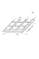
- FIG. 1 is a perspective view of a circuit board according to one embodiment.
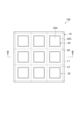
- FIG. 2 is a plan view of a circuit board according to one embodiment.
- FIG. 3 is a cross-sectional view taken along the line III--III of the circuit board of FIG.
- FIG. 4 is an enlarged cross-sectional view of a part of the cross-section of FIG. 3.
- FIG. 5 is a scanning electron microscope (SEM) photograph showing an example of a cross section along the thickness direction of the circuit board.
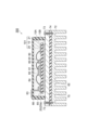
- FIG. 6 is a cross-sectional view of the power module.
- FIG. 7 is a scanning electron microscope (SEM) photograph showing a cross section along the thickness direction of the circuit board of Comparative Example 1.
- the numerical range indicated by "x to y” means greater than or equal to x and less than or equal to y.
- Numerical ranges in which the upper limit or lower limit of each numerical range in each embodiment is replaced with the numerical value of any example are also included in the present disclosure.
- a circuit board includes a ceramic plate, a metal plate, and a brazing material layer that joins the main surface of the ceramic plate and the main surface of the metal plate.
- the number of metal plates joined to one main surface of one ceramic plate may be one or multiple.
- the material of the ceramic plate is not particularly limited, and may be made of, for example, a nitride sintered body, a carbide sintered body, or an oxide sintered body. Specific examples include silicon nitride sintered bodies, aluminum nitride sintered bodies, aluminum oxide sintered bodies, and silicon carbide sintered bodies. There is no particular restriction as long as it is in the shape of a ceramic plate.
- the thickness of the ceramic plate may be, for example, 0.2 to 2 mm, or 0.32 to 1.1 mm.
- the metal plate may be a copper plate, for example.
- the shape of the metal plate is not particularly limited as long as a recess is formed along at least a part of the outer edge of the main surface opposite to the main surface of the ceramic plate.
- the thickness of the metal plate (distance between main surfaces) may be, for example, 0.1 to 1.2 mm, or 0.2 to 1.0 mm.
- the metal plate may have a plating film on its surface.
- the recess may be formed by a curved wall surface. That is, the metal plate may have an inner corner in the recess. This corner may extend parallel to the edge of the recess on the side surface of the metal plate.
- the brazing material layer may contain silver and copper, and may further contain one or more metals selected from the group consisting of tin and active metals. Two or more metals may be an alloy.
- the active metal may include one or more selected from the group consisting of titanium, hafnium, zirconium, and niobium.
- Silver and copper contained in the brazing material layer may be contained in the brazing material layer as an alloy such as an Ag--Cu eutectic alloy.
- the content of silver in the brazing material layer may be 45 to 95% by mass, or 50 to 95% by mass in terms of Ag.
- the total content of silver and copper in the brazing material layer may be 65 to 100% by mass, 70 to 99% by mass, or 90 to 98% by mass in terms of Ag and Cu, respectively. good. This makes it possible to sufficiently reduce the residual stress in the brazing material layer and improving the denseness of the brazing material layer.
- the content of the active metal in the brazing material layer may be 0.5 to 8 parts by mass based on 100 parts by mass of Ag and Cu in total.
- the content of the active metal may be 0.5 to 8 parts by mass based on 100 parts by mass of Ag and Cu in total.
- the metal contained in the brazing material layer may be contained as a nitride, oxide, carbide, or hydride.
- the braze layer may include titanium nitride and/or titanium hydride ( TiH2 ). This makes it possible to sufficiently increase the bonding strength between the ceramic plate and the metal plate.
- TiH 2 titanium nitride and/or titanium hydride
- the content of TiH 2 may be, for example, 1 to 8 parts by weight based on 100 parts by weight of Ag and Cu in total.
- FIG. 1 is a perspective view showing an example of a circuit board according to the present embodiment.
- 2 is a plan view of the circuit board of FIG. 1
- FIG. 3 is a sectional view taken along the line III--III of FIG.
- the circuit board 100 includes a ceramic plate 10 and a plurality of metal plates 20 on the main surface 10A and the main surface 10B of the ceramic board 10.
- the ceramic plate 10 has a flat plate shape.
- the ceramic plate 10 is divided into a plurality of sections by dividing lines on the main surface 10A.
- the principal surface 10A includes a plurality of partition lines L1 extending along a first direction and lined up at equal intervals, and a plurality of partition lines L1 extending along a second direction orthogonal to the first direction, as partition lines.
- a plurality of partition lines L2 arranged at equal intervals are provided.
- the partition line L1 and the partition line L2 are orthogonal to each other.
- the partition lines L1 and L2 may be formed by, for example, a plurality of recesses lined up in a straight line, or may have a linear groove formed therein. Specifically, it may be a scribe line formed with laser light. Examples of the laser source include a carbon dioxide laser and a YAG laser. A scribe line can be formed by intermittently irradiating laser light from such a laser source. Note that the partition lines L1 and L2 do not have to be arranged at equal intervals, and are not limited to being perpendicular to each other. Further, the partition lines L1 and L2 may not be straight, but may be curved or bent.
- the ceramic plate 10 has a plurality of partition areas 50 defined by partition lines L1 and L2.
- a metal plate 20 is provided in each of the plurality of divided areas 50.
- the plurality of metal plates 20 are independent from each other.
- the circuit board 100 is also called a collective board, and can be divided along partition lines L1 and L2. By dividing, a plurality of circuit boards (singulated boards) can be obtained. The individualized board obtained by dividing in this way is also an example of the circuit board of this embodiment.
- One main surface 20A of the metal plate 20 is exposed to the outside.
- the other main surface 20B of the metal plate 20 and the main surface 10A (main surface 10B) of the ceramic plate 10 are joined by a brazing material layer 30.
- a recess 22 is formed in the metal plate 20 along the outer edge of the main surface 20B (joint surface with the brazing material layer 30) of the metal plate 20.
- the metal plate 20 having such a recess 22 formed therein may be cut out so that the outer side of the main surface 20B has a step-like shape. As shown in FIG. 2, the recess 22 is formed all around the outer edge of the main surface 20B of the metal plate 20. That is, the outer edge of the main surface 20B is formed by the recess 22.
- the recess 22 may be provided only in the vicinity of the portion where the semiconductor element is soldered when the semiconductor element is mounted on the metal plate 20. Further, the recesses 22 may be provided only in some of the plurality of metal plates 20. For example, it is not necessary to provide the recess 22 in the metal plate 20 that serves as a heat sink of the power module.
- FIG. 4 shows a partially enlarged cross-section of the circuit board 100 shown in FIG. 3.
- 3 and 4 both show a cross section along the thickness direction of the metal plate 20, perpendicular to the edge 27 of the recess 22 on the side surface 20C of the metal plate 20.
- the width X of the recess 22 may be 0.05 mm or more, 0.2 mm or more, or 0.4 mm or more. In this way, as the width X increases, the distance from the brazing material layer 30 to the side surface 20C of the metal plate 20 increases. Therefore, creeping up of the brazing material onto the main surface 20A can be further suppressed.
- the width X may be 10 mm or less, 5 mm or less, 3 mm or less, 1.3 mm or less, or 1 mm or less.
- the ratio of the width X to the length of the main surface 20A of the metal plate 20 measured along the same direction as the width X may be 0.0005 to 0.5, and may be 0.001 to 0.3. It may be between 0.005 and 0.3.
- the length of the main surface 20A may be, for example, 5 to 100 mm, or 15 to 50 mm.
- the height Z of the recess 22 may be 0.05 mm or more, 0.2 mm or more, or 0.3 mm or more. In this way, as the height Z increases, the distance from the brazing material layer 30 to the side surface 20C of the metal plate 20 increases. Therefore, creeping up of the brazing material onto the main surface 20A of the metal plate 20 can be further suppressed.
- the height Z may be 1.1 mm or less, 0.6 mm or less, or 0.5 mm or less.
- the ratio of the height Z to the thickness of the metal plate 20 may be 0.04 to 1.0, or may be 0.1 to 0.6.
- the ratio of the height Z to the width X may be 0.001 to 22, and may be 0.1 to 4. It may be 0.15 to 3. Note that the width X is measured along a direction parallel to the main surfaces 10A and 10B of the ceramic plate 10 in the cross section shown in FIGS. 3 and 4. The height Z is measured along the direction perpendicular to the main surfaces 10A and 10B of the ceramic plate 10 in the cross section shown in FIGS. 3 and 4.
- the wall surface of the metal plate 20 constituting the recess 22 includes an opposing surface 24 that faces the main surfaces 10A and 10B of the ceramic plate 10, and an upright surface 23 that is orthogonal to the main surfaces 10A and 10B. At the boundary between the opposing surface 24 and the upright surface 23, an inside corner 25 extends parallel to the edge 27 of the recess 22. Since the metal plate 20 has the opposing surface 24 and the corner portion 25 in the recess 22, it is possible to further suppress the brazing material from creeping up from the brazing material layer 30.
- the upright surface 23 is perpendicular to the main surfaces 10A and 10B, but is not limited thereto.
- the facing surface 24 and/or the upright surface 23 may be inclined with respect to the main surface 10A and the main surface 10B.
- the width X and height Z are as shown in FIG.
- the width X and height Z are measured based on the most recessed part of the recess 22.
- the width X is measured based on the most outwardly protruding portion of the side surface 20C. That is, the width X can be determined as the maximum value of the distance between the side surface 20C and the wall surface constituting the recess, measured in a direction parallel to the main surface 20A in a cross section as shown in FIG.
- the height Z is the height between the main surface 10A (main surface 10B) and the wall surface (opposing surface 24) forming the recess 22, measured in a direction perpendicular to the main surface 20A in a cross section as shown in FIG. It can be determined as the maximum value of distance.
- FIG. 5 is a SEM photograph showing an example of a cross section along the thickness direction of the circuit board. Similar to FIG. 4, FIG. 5 shows a partially enlarged cross section of the side surface 20C of the metal plate 20, which is perpendicular to the edge 27 of the recess 22 and along the thickness direction of the metal plate 20.
- a rising portion 32 is formed at the end of the brazing material layer 30.
- the rising portion 32 has a substantially triangular shape below the inner corner portion 25 .
- the rising portion 32 has an inclined portion 32A that widens as it approaches the main surface 10A of the ceramic plate 10 inside the recessed portion 22. By having such an inclined portion 32A, creeping up of the brazing material onto the main surface 20A of the metal plate 20 can be further suppressed.
- the bonding area between the metal plate 20 and the ceramic plate 10 by the brazing material layer 30 can be increased, and the bonding strength can be increased.
- the size of the inclined portion 32A can be adjusted by changing the composition of the brazing material, the heating temperature and heating time during bonding, and the like.
- the metal plate 20 may function as a circuit board that has the function of transmitting electrical signals or a heat sink that has the function of transmitting heat. Further, the metal plate 20 may have both a function of transmitting heat and a function of transmitting an electric signal.
- the circuit board 100 and the individualized boards (circuit boards) obtained by dividing the same creeping up of the brazing material on the main surface 20A of the metal plate 20 on the side opposite to the ceramic plate side is suppressed. Therefore, it has excellent appearance and connection reliability with external circuits such as semiconductor elements. Therefore, it is suitable as a component mounted on a power module that requires high reliability.
- a power module includes a circuit board and a semiconductor element electrically connected to a metal plate of the circuit board.
- the circuit board may be the above-described circuit board 100 or a modification thereof, or may be another circuit board. The description regarding the circuit board 100 and its modifications is applied to the power module of this embodiment. Such a power module has excellent reliability.
- the circuit board and the semiconductor element may be sealed with resin.
- FIG. 6 is a cross-sectional view showing an example of the power module according to the present embodiment.
- the power module 300 includes a base plate 70 and a circuit board 101 joined to one side of the base plate 70 via solder 62.
- the metal plate 21 on one side of the circuit board 101 is joined to the base plate 70 via solder 62.
- a semiconductor element 60 is attached to at least one of the metal plates 20 on the other side of the circuit board 101 via solder 61.
- the semiconductor element 60 is connected to a predetermined location on the metal plate 20 with a metal wire 64 such as an aluminum wire. In this way, the semiconductor element 60 and the metal plate 20 are electrically connected.
- the metal plate 20a which is one of the metal plates 20, is connected to an electrode 63 provided through the casing 66 via a solder 65. ing.
- a housing 66 is disposed on one main surface of the base plate 70 and is integrated with the main surface to accommodate the circuit board 101.
- a housing space formed by one main surface of the base plate 70 and the housing 66 is filled with resin 80.
- the resin 80 seals the circuit board 101 and the semiconductor element 60.
- the resin may be, for example, a thermosetting resin or a photocuring resin.
- Cooling fins 72 forming a heat radiating section are joined to the other main surface of the base plate 70 via grease 74. Screws 73 are attached to the ends of the base plate 70 to fix the cooling fins 72 to the base plate 70.
- the base plate 70 and the cooling fins 72 may be made of aluminum.
- the base plate 70 and the cooling fins 72 have high thermal conductivity and function well as a heat dissipation section.
- the metal plate 20 and the metal plate 21 are electrically insulated by the ceramic plate 10.
- the metal plate 20 (20a) may form an electric circuit.
- the metal plate 20 and the metal plate 21 are respectively joined to the main surface 10A and the main surface 10B of the ceramic plate 10 by a brazing material layer (not shown).
- the metal plate 20 is formed with recesses as shown in FIGS. 1 to 5. This recess has the same size as the recess 22, and at least a portion of the wall surface of the metal plate 20 forming the recess may be covered with a brazing material layer. As a result, creeping up of the brazing material on the main surface of the metal plate 20 on which the semiconductor element 60 is mounted is sufficiently suppressed. Further, the recessed portion is sufficiently filled with resin 80. Therefore, the power module 300 has excellent electrical connection reliability between the semiconductor element 60 and the metal plate 20.
- the metal plate 21 may also have a recess 22 formed therein.
- a method for manufacturing a circuit board includes a preparation step of preparing one or more metal plates each having a recess formed along the outer edge of one main surface, and applying a brazing material to the main surface of the ceramic plate.
- a coating and drying process in which one or more coating layers are formed by coating and drying, and lamination in which a ceramic plate and one or more metal plates are laminated with one or more coating layers sandwiched therebetween to produce a laminate. and a joining step of heating the laminate to obtain a joined body in which a ceramic plate and one or more metal plates are joined with one or more brazing metal layers.
- the metal plate may be a copper plate, for example.
- the recessed portion can be formed, for example, by machining using a machining center.
- the size of the recess, ie width X and height Z, may be as described above.
- the recess may be formed in a part of the outer edge of the main surface of the metal plate, or may be formed by cutting the outer edge of the main surface of the metal plate over the entire circumference.
- the ceramic plate used in the coating and drying process can be produced, for example, by the following procedure.
- a green sheet is produced by molding a slurry containing an inorganic compound powder, a binder resin, a sintering aid, a plasticizer, a dispersant, a solvent, and the like.
- inorganic compounds include aluminum nitride (AlN), silicon nitride (Si 3 N 4 ), silicon carbide, and aluminum oxide.
- Sintering aids include rare earth metals, alkaline earth metals, metal oxides, fluorides, chlorides, nitrates, sulfates, and the like. These may be used alone or in combination of two or more.
- binder resins include methyl cellulose, ethyl cellulose, polyvinyl alcohol, polyvinyl butyral, and (meth)acrylic resins.
- plasticizers include purified glycerin, glycerin triolate, diethylene glycol, phthalic acid plasticizers such as di-n-butyl phthalate, and dibasic acid plasticizers such as di-2-ethylhexyl sebacate.
- dispersants include poly(meth)acrylates and (meth)acrylic acid-maleate copolymers.
- solvents include organic solvents such as ethanol and toluene.
- Examples of methods for forming green sheets include a doctor blade method and an extrusion method.
- the green sheet obtained by molding the slurry is degreased and sintered.
- Degreasing may be performed, for example, by heating at 400 to 800°C for 0.5 to 20 hours. Thereby, the amount of residual organic matter (carbon) can be reduced while suppressing oxidation and deterioration of inorganic compounds.
- Sintering is performed by heating to 1700 to 1900° C. in a non-oxidizing gas atmosphere such as nitrogen, argon, ammonia, or hydrogen. In this way, for example, a ceramic plate 10 can be obtained. If necessary, the ceramic plate may be laser-processed to cut the edges or provide scribe lines.
- the above-mentioned degreasing and sintering may be performed, for example, with a plurality of green sheets laminated.
- a release layer made of a release agent may be provided between the green sheets to facilitate separation of the base materials after sintering.
- the mold release agent for example, boron nitride (BN) can be used.
- the release layer may be formed, for example, by applying a slurry of boron nitride powder by spraying, brushing, roll coating, screen printing, or the like.
- the number of green sheets to be laminated may be, for example, 8 to 100, or 30 to 70, from the viewpoint of efficient mass production of ceramic plates and sufficient degreasing.
- a partition line may be formed on the one main surface.
- a scribe line may be provided as a partition line by irradiating the main surface of the ceramic plate with a laser beam.
- the laser beam irradiated onto the main surface of the ceramic include a carbon dioxide laser and a YAG laser.
- scribe lines that become the partition lines L1 and L2 as shown in FIGS. 1 and 2 are formed.
- Such partition lines L1 and L2 can be used as cutting lines when dividing the circuit board in a subsequent process.
- the brazing material applied to the main surface of the ceramic plate contains, for example, silver, copper, tin, active metals, metal compounds containing these as constituent elements, organic solvents, binders, and the like.
- the viscosity of the brazing filler metal may be, for example, 5 to 20 Pa ⁇ s.
- the organic solvent content in the brazing filler metal may be, for example, 5 to 25% by mass, and the binder content may be, for example, 2 to 15% by mass.
- the brazing filler metal may contain silver in the form of a single metal or a metal compound (alloy), and in addition to silver, it may contain one or more metals selected from the group consisting of copper, tin, and active metals. It's fine. Two or more metals may be an alloy.
- the active metal may include one or more selected from the group consisting of titanium, hafnium, zirconium, and niobium.
- the content of silver in the brazing filler metal may be 45 to 95% by mass, or 50 to 95% by mass in terms of Ag.
- the total content of silver and copper in the brazing material may be 65 to 100% by mass, 70 to 99% by mass, or 90 to 98% by mass in terms of Ag and Cu, respectively. . This makes it possible to sufficiently reduce the residual stress in the brazing material layer formed in a subsequent process and improving the density of the brazing material layer.
- the content of active metal in the brazing material may be 0.5 to 8 parts by mass based on 100 parts by mass of Ag and Cu in total.
- the content of the active metal may be 0.5 to 8 parts by mass based on 100 parts by mass of Ag and Cu in total.
- the metal contained in the brazing filler metal may be contained as a nitride, oxide, carbide, or hydride.
- the brazing material may include titanium nitride and/or titanium hydride ( TiH2 ). This makes it possible to sufficiently increase the bonding strength between the ceramic plate and the metal plate.
- TiH 2 titanium nitride and/or titanium hydride
- the content of TiH 2 may be, for example, 1 to 8 parts by weight based on 100 parts by weight of Ag and Cu in total.
- the content of tin in the brazing filler metal may be 0.5 to 5 parts by mass based on 100 parts by mass of Ag and Cu in total.
- the tin content may be 0.5 to 5 parts by mass based on 100 parts by mass of Ag and Cu in total.
- One or more coating layers are provided on the main surface of the ceramic plate by applying and drying a brazing material by a method such as a roll coater method, screen printing method, or transfer method.
- the coating layer may be provided at a position where the metal plates are to be joined. Therefore, the number of coated layers may be the same as the number of metal plates bonded to the ceramic plate.
- the coating layer is formed, a ceramic plate and a metal plate are laminated with the coating layer sandwiched between them to produce a laminate.
- the two main surfaces of the metal plates are stacked such that the main surface on which the recess is formed faces the main surface of the ceramic plate.
- the metal plate may be pressed in the direction toward the ceramic plate. As the pressure is applied, the coating layer spreads, and a laminate in which the ceramic plate and the metal plate are well bonded by the coating layer is obtained.
- each of the plurality of metal plates 20 is arranged independently for each partition area 50 defined by partition lines L1 and L2 on the main surface 10A of the ceramic plate 10.
- a plurality of metal plates 20 are laminated to produce a laminate.
- the obtained laminate is heated in a heating furnace to obtain a joined body in which the ceramic plate and the metal plate are joined with a brazing material layer.
- the heating temperature may be, for example, 700 to 900°C.
- the atmosphere in the furnace may be an inert gas such as nitrogen, and the reaction may be performed under reduced pressure below atmospheric pressure or under vacuum.
- the heating furnace may be of a continuous type that continuously manufactures a plurality of joined bodies, or may be one that manufactures one or more joined bodies in a batch manner. Heating may be performed while pressing the joined body in the stacking direction of the laminate.
- the brazing material contained in the coating layer flows and reacts with the metal plate, forming a brazing material layer.
- the brazing material layer may include a reaction product between the brazing material and a metal component contained in the metal plate.
- a portion of the brazing material may climb up the wall surface of the metal plate constituting the recess, forming a climbing portion 32 as shown in FIG.
- surface treatment such as forming a plating film on the metal plate is performed.
- cutting or the like may be performed to adjust the shape of the brazing material layer. In this way, a circuit board can be manufactured.
- a dividing step may be performed in which the aggregate substrate is divided into individual pieces. .
- the collective board can be divided along the division lines L1 and L2 to obtain a plurality of circuit boards.
- a joined body can be obtained by joining a plurality of metal plates that have been previously processed to a predetermined size.
- a circuit board in which creeping up is suppressed can be efficiently manufactured without performing a resist printing process and a metal plate etching process.
- the circuit board obtained by such a manufacturing method can reduce manufacturing costs and has excellent appearance and connection reliability with external circuits such as semiconductor elements.
- the manufacturing method of the circuit boards 100, 101 and their modifications described above is not limited to the manufacturing method described above.
- a power module may be manufactured using the circuit board obtained in this way.
- a power module can be manufactured by mounting a semiconductor element on a circuit board using solder and wire bonding, etc., housing the circuit board and semiconductor element in a housing space of a housing, and then sealing it with resin. .
- a plurality of metal plates are provided on each of the pair of main surfaces of the ceramic plate, but the present invention is not limited thereto.
- one or more metal plates may be provided on only one main surface of the ceramic plate.
- the structure and shape of the brazing material layer and the metal plate provided on each of the pair of main surfaces of the ceramic plate may be different from each other.
- one metal plate may be provided on each of the pair of main surfaces of the ceramic plate.
- the recess does not need to be provided so as to surround the main surface.
- a circuit board comprising a ceramic plate, a metal plate, and a brazing material layer that joins the main surface of the ceramic plate and the main surface of the metal plate, A circuit board, wherein a recess is formed in the metal plate along at least a part of an outer edge of the main surface of the metal plate.
- a circuit board wherein the recess in the metal plate is formed all around the outer edge of the main surface of the metal plate.
- the wall surface of the metal plate forming the recess includes a facing surface facing the main surface of the ceramic plate.
- Substrate manufacturing method [8]
- a plurality of metal plates in which the recesses are formed are prepared
- the laminated body is produced by laminating the plurality of metal plates such that each of the plurality of metal plates is independent for each partition area defined by a partition line on the main surface of the ceramic plate.
- a power module comprising: a semiconductor element electrically connected to the semiconductor element;
- a brazing filler metal containing Ag, Cu, Sn, and TiH2 was prepared.
- the mass ratio of Ag to Cu in the brazing filler metal was 9:1.
- This brazing filler metal contained 3 parts by mass of Sn and 3.5 parts by mass of TiH 2 based on 100 parts by mass of Ag and Cu in total.
- the main surface of the ceramic plate was divided into 24 divided areas by scribe lines.
- a brazing material was applied to each section by screen printing to form a coating layer.
- the coating area of the coating layer was the same as the area of the main surface of the copper plate to be bonded to the ceramic plate.
- a copper plate was laminated on the ceramic plate so that the coating layer and the main surface of the copper plate were in contact with each other. In this way, a total of 24 copper plates were laminated on one main surface of the ceramic plate so that each section was independent.
- FIG. 5 is a SEM photograph of a cross section of the circuit board of Example 1. The measurement results were as shown in Table 1. The measurements were performed on only one circuit board. Note that all 24 copper plates were processed under the same machining conditions. Therefore, the values of the width X and height Z of the recess can be considered to be the same.
- the ceramic circuit board was cut perpendicular to the edge of the recess on the side surface of the metal plate and along the thickness direction of the copper plate.
- the obtained cut surface was confirmed with a microscope (magnification: 250 times) to evaluate the ability to fill the recesses of the copper plate with the resin.
- the case where the entire recess was filled with resin was rated "A"
- the case where only a part of the recess was filled with resin was rated "B".
- Example 2 The procedure was the same as in Example 1, except that the amount of cutting of the outer edge on one main surface of the copper plate by machining was changed, and the width X and height Z of the recess in the copper plate were changed as shown in Table 1. A circuit board was created. Then, the circuit board was evaluated in the same manner as in Example 1. The evaluation results were as shown in Table 1.
- FIG. 7 is an SEM photograph of a cross section of the circuit board of Comparative Example 1. As shown in FIG. 7, the copper plate 120 and the ceramic plate 110 were joined via the brazing material layer 130. The brazing material had even reached the main surface on the opposite side from the ceramic plate 110 side.
- SYMBOLS 10 110... Ceramic plate, 10A, 10B... Main surface, 20, 20a... Metal plate, 20A... Main surface, 20B... Main surface, 20C... Side surface, 22... Recessed part, 23... Standing surface, 24... Opposing surface, 25... Inner corner, 27... Edge, 30, 130... Brazing material layer, 32... Rising portion, 32A... Inclined portion, 50... Division area, 60... Semiconductor element, 61, 62, 65... Solder, 63... Electrode, 64... Metal wire, 66... Housing, 70... Base plate, 72... Cooling fin, 73... Screw, 74... Grease, 80... Resin, 100, 101... Circuit board, 110... Ceramic board, 120... Copper plate, 300...power module, L1, L2...compartment line.
Landscapes
- Engineering & Computer Science (AREA)
- Chemical & Material Sciences (AREA)
- Microelectronics & Electronic Packaging (AREA)
- Ceramic Engineering (AREA)
- Materials Engineering (AREA)
- Structural Engineering (AREA)
- Organic Chemistry (AREA)
- Structure Of Printed Boards (AREA)
Priority Applications (1)
| Application Number | Priority Date | Filing Date | Title |
|---|---|---|---|
| JP2024512409A JPWO2023190246A1 (https=) | 2022-03-31 | 2023-03-24 |
Applications Claiming Priority (2)
| Application Number | Priority Date | Filing Date | Title |
|---|---|---|---|
| JP2022-059779 | 2022-03-31 | ||
| JP2022059779 | 2022-03-31 |
Publications (1)
| Publication Number | Publication Date |
|---|---|
| WO2023190246A1 true WO2023190246A1 (ja) | 2023-10-05 |
Family
ID=88201638
Family Applications (1)
| Application Number | Title | Priority Date | Filing Date |
|---|---|---|---|
| PCT/JP2023/011999 Ceased WO2023190246A1 (ja) | 2022-03-31 | 2023-03-24 | 回路基板及びその製造方法、並びにパワーモジュール |
Country Status (2)
| Country | Link |
|---|---|
| JP (1) | JPWO2023190246A1 (https=) |
| WO (1) | WO2023190246A1 (https=) |
Citations (2)
| Publication number | Priority date | Publication date | Assignee | Title |
|---|---|---|---|---|
| JP2017011216A (ja) * | 2015-06-25 | 2017-01-12 | 京セラ株式会社 | 回路基板および電子装置 |
| JP2022000871A (ja) * | 2018-07-31 | 2022-01-04 | 京セラ株式会社 | 電気回路基板及びパワーモジュール |
Family Cites Families (2)
| Publication number | Priority date | Publication date | Assignee | Title |
|---|---|---|---|---|
| JP2014086581A (ja) * | 2012-10-24 | 2014-05-12 | Nippon Steel & Sumikin Electronics Devices Inc | 半導体素子収納用パッケージ |
| WO2019163941A1 (ja) * | 2018-02-22 | 2019-08-29 | 京セラ株式会社 | パワーモジュール用基板およびパワーモジュール |
-
2023
- 2023-03-24 WO PCT/JP2023/011999 patent/WO2023190246A1/ja not_active Ceased
- 2023-03-24 JP JP2024512409A patent/JPWO2023190246A1/ja active Pending
Patent Citations (2)
| Publication number | Priority date | Publication date | Assignee | Title |
|---|---|---|---|---|
| JP2017011216A (ja) * | 2015-06-25 | 2017-01-12 | 京セラ株式会社 | 回路基板および電子装置 |
| JP2022000871A (ja) * | 2018-07-31 | 2022-01-04 | 京セラ株式会社 | 電気回路基板及びパワーモジュール |
Also Published As
| Publication number | Publication date |
|---|---|
| JPWO2023190246A1 (https=) | 2023-10-05 |
Similar Documents
| Publication | Publication Date | Title |
|---|---|---|
| US6261703B1 (en) | Copper circuit junction substrate and method of producing the same | |
| JP7555397B2 (ja) | 回路基板、接合体、及びこれらの製造方法 | |
| KR20120098637A (ko) | 파워 모듈용 기판, 히트싱크가 부착된 파워 모듈용 기판, 파워 모듈, 파워 모듈용 기판의 제조 방법 및 히트싱크가 부착된 파워 모듈용 기판의 제조 방법 | |
| JP2021031310A (ja) | セラミックス基板、回路基板及びその製造方法、並びにパワーモジュール | |
| JP6182903B2 (ja) | セラミック回路基板の製造方法 | |
| JP7666202B2 (ja) | 銅/セラミックス接合体、および、絶縁回路基板 | |
| JP7535198B2 (ja) | 回路基板及びその製造方法、並びにパワーモジュール | |
| WO2023190246A1 (ja) | 回路基板及びその製造方法、並びにパワーモジュール | |
| WO2023190253A1 (ja) | 回路基板及びその製造方法、並びにパワーモジュール | |
| WO2025027879A1 (ja) | パッケージ、半導体モジュール、およびパッケージの製造方法 | |
| WO2023190255A1 (ja) | 回路基板及びその製造方法、並びにパワーモジュール | |
| JP5828391B2 (ja) | 接合冶具およびそれを用いた接合冶具ユニット | |
| EP3961694B1 (en) | Electronic component module and silicon nitride circuit substrate | |
| CN119547203A (zh) | 多层接合体及使用该多层接合体的半导体装置、以及它们的制造方法 | |
| JP3447043B2 (ja) | 電子部品用パッケージ | |
| JP7555493B2 (ja) | 回路基板及びその製造方法 | |
| WO2025169687A1 (ja) | 回路基板及びその製造方法、回路基板群、並びにパワーモジュール | |
| KR20210142616A (ko) | 질화규소 회로 기판, 및, 전자 부품 모듈 | |
| JP2026006113A (ja) | 接合体及びその製造方法、並びにパワーモジュール | |
| JP7208439B2 (ja) | セラミックス回路基板、電子デバイス、金属部材、及びセラミックス回路基板の製造方法 | |
| WO2025134898A1 (ja) | セラミックス回路基板及びその製造方法 | |
| JP7708622B2 (ja) | セラミック複合基板 | |
| JP2025053936A (ja) | 回路基板及びその製造方法 | |
| JPH05211248A (ja) | 半導体搭載用複合放熱基板及びその製造方法 | |
| EP4033524A1 (en) | Circuit board and module comprising same |
Legal Events
| Date | Code | Title | Description |
|---|---|---|---|
| 121 | Ep: the epo has been informed by wipo that ep was designated in this application |
Ref document number: 23780256 Country of ref document: EP Kind code of ref document: A1 |
|
| ENP | Entry into the national phase |
Ref document number: 2024512409 Country of ref document: JP Kind code of ref document: A |
|
| NENP | Non-entry into the national phase |
Ref country code: DE |
|
| 122 | Ep: pct application non-entry in european phase |
Ref document number: 23780256 Country of ref document: EP Kind code of ref document: A1 |