WO2023190246A1 - Printed circuit board and manufacturing method therefor, and power module - Google Patents
Printed circuit board and manufacturing method therefor, and power module Download PDFInfo
- Publication number
- WO2023190246A1 WO2023190246A1 PCT/JP2023/011999 JP2023011999W WO2023190246A1 WO 2023190246 A1 WO2023190246 A1 WO 2023190246A1 JP 2023011999 W JP2023011999 W JP 2023011999W WO 2023190246 A1 WO2023190246 A1 WO 2023190246A1
- Authority
- WO
- WIPO (PCT)
- Prior art keywords
- main surface
- circuit board
- metal
- plate
- metal plate
- Prior art date
Links
- 238000004519 manufacturing process Methods 0.000 title claims description 28
- 229910052751 metal Inorganic materials 0.000 claims abstract description 244
- 239000002184 metal Substances 0.000 claims abstract description 244
- 239000000919 ceramic Substances 0.000 claims abstract description 118
- 238000005219 brazing Methods 0.000 claims abstract description 107
- 239000004065 semiconductor Substances 0.000 claims abstract description 25
- 238000005304 joining Methods 0.000 claims abstract description 9
- 239000000463 material Substances 0.000 claims description 79
- 239000010410 layer Substances 0.000 claims description 54
- 238000000034 method Methods 0.000 claims description 33
- 238000005192 partition Methods 0.000 claims description 25
- 239000000945 filler Substances 0.000 claims description 24
- 239000011247 coating layer Substances 0.000 claims description 19
- 238000010438 heat treatment Methods 0.000 claims description 12
- 238000010030 laminating Methods 0.000 claims description 12
- 238000001035 drying Methods 0.000 claims description 10
- 239000011248 coating agent Substances 0.000 claims description 8
- 238000000576 coating method Methods 0.000 claims description 8
- 238000002360 preparation method Methods 0.000 claims description 8
- 239000000758 substrate Substances 0.000 claims description 5
- 238000013459 approach Methods 0.000 claims description 4
- 239000010949 copper Substances 0.000 description 47
- 229910052802 copper Inorganic materials 0.000 description 45
- RYGMFSIKBFXOCR-UHFFFAOYSA-N Copper Chemical compound [Cu] RYGMFSIKBFXOCR-UHFFFAOYSA-N 0.000 description 36
- 229920005989 resin Polymers 0.000 description 19
- 239000011347 resin Substances 0.000 description 19
- 229910052709 silver Inorganic materials 0.000 description 18
- 239000004332 silver Substances 0.000 description 9
- 238000005245 sintering Methods 0.000 description 8
- 239000011135 tin Substances 0.000 description 8
- 229910045601 alloy Inorganic materials 0.000 description 7
- 239000000956 alloy Substances 0.000 description 7
- 150000002739 metals Chemical class 0.000 description 7
- 229910000679 solder Inorganic materials 0.000 description 7
- 229910052718 tin Inorganic materials 0.000 description 7
- ATJFFYVFTNAWJD-UHFFFAOYSA-N Tin Chemical compound [Sn] ATJFFYVFTNAWJD-UHFFFAOYSA-N 0.000 description 6
- 238000001816 cooling Methods 0.000 description 5
- 238000011156 evaluation Methods 0.000 description 5
- 238000003475 lamination Methods 0.000 description 5
- 229910000048 titanium hydride Inorganic materials 0.000 description 5
- IJGRMHOSHXDMSA-UHFFFAOYSA-N Atomic nitrogen Chemical compound N#N IJGRMHOSHXDMSA-UHFFFAOYSA-N 0.000 description 4
- CURLTUGMZLYLDI-UHFFFAOYSA-N Carbon dioxide Chemical compound O=C=O CURLTUGMZLYLDI-UHFFFAOYSA-N 0.000 description 4
- PEDCQBHIVMGVHV-UHFFFAOYSA-N Glycerine Chemical compound OCC(O)CO PEDCQBHIVMGVHV-UHFFFAOYSA-N 0.000 description 4
- 239000011230 binding agent Substances 0.000 description 4
- 230000000052 comparative effect Effects 0.000 description 4
- 238000005520 cutting process Methods 0.000 description 4
- 238000005238 degreasing Methods 0.000 description 4
- 238000005530 etching Methods 0.000 description 4
- 150000002484 inorganic compounds Chemical class 0.000 description 4
- 229910010272 inorganic material Inorganic materials 0.000 description 4
- 238000003754 machining Methods 0.000 description 4
- 239000004014 plasticizer Substances 0.000 description 4
- 238000007747 plating Methods 0.000 description 4
- 230000000630 rising effect Effects 0.000 description 4
- 229910052581 Si3N4 Inorganic materials 0.000 description 3
- YXFVVABEGXRONW-UHFFFAOYSA-N Toluene Chemical compound CC1=CC=CC=C1 YXFVVABEGXRONW-UHFFFAOYSA-N 0.000 description 3
- 230000015572 biosynthetic process Effects 0.000 description 3
- MTHSVFCYNBDYFN-UHFFFAOYSA-N diethylene glycol Chemical compound OCCOCCO MTHSVFCYNBDYFN-UHFFFAOYSA-N 0.000 description 3
- 239000003822 epoxy resin Substances 0.000 description 3
- 230000001678 irradiating effect Effects 0.000 description 3
- 238000005259 measurement Methods 0.000 description 3
- 238000012986 modification Methods 0.000 description 3
- 230000004048 modification Effects 0.000 description 3
- 150000004767 nitrides Chemical class 0.000 description 3
- 239000003960 organic solvent Substances 0.000 description 3
- 229920000647 polyepoxide Polymers 0.000 description 3
- 239000000843 powder Substances 0.000 description 3
- 238000007650 screen-printing Methods 0.000 description 3
- HQVNEWCFYHHQES-UHFFFAOYSA-N silicon nitride Chemical compound N12[Si]34N5[Si]62N3[Si]51N64 HQVNEWCFYHHQES-UHFFFAOYSA-N 0.000 description 3
- 239000002002 slurry Substances 0.000 description 3
- QGZKDVFQNNGYKY-UHFFFAOYSA-N Ammonia Chemical compound N QGZKDVFQNNGYKY-UHFFFAOYSA-N 0.000 description 2
- XKRFYHLGVUSROY-UHFFFAOYSA-N Argon Chemical compound [Ar] XKRFYHLGVUSROY-UHFFFAOYSA-N 0.000 description 2
- PZNSFCLAULLKQX-UHFFFAOYSA-N Boron nitride Chemical compound N#B PZNSFCLAULLKQX-UHFFFAOYSA-N 0.000 description 2
- LFQSCWFLJHTTHZ-UHFFFAOYSA-N Ethanol Chemical compound CCO LFQSCWFLJHTTHZ-UHFFFAOYSA-N 0.000 description 2
- RTAQQCXQSZGOHL-UHFFFAOYSA-N Titanium Chemical compound [Ti] RTAQQCXQSZGOHL-UHFFFAOYSA-N 0.000 description 2
- NRTOMJZYCJJWKI-UHFFFAOYSA-N Titanium nitride Chemical compound [Ti]#N NRTOMJZYCJJWKI-UHFFFAOYSA-N 0.000 description 2
- QCWXUUIWCKQGHC-UHFFFAOYSA-N Zirconium Chemical compound [Zr] QCWXUUIWCKQGHC-UHFFFAOYSA-N 0.000 description 2
- 229910052782 aluminium Inorganic materials 0.000 description 2
- XAGFODPZIPBFFR-UHFFFAOYSA-N aluminium Chemical compound [Al] XAGFODPZIPBFFR-UHFFFAOYSA-N 0.000 description 2
- 239000012298 atmosphere Substances 0.000 description 2
- 229910002092 carbon dioxide Inorganic materials 0.000 description 2
- 239000001569 carbon dioxide Substances 0.000 description 2
- 239000003795 chemical substances by application Substances 0.000 description 2
- 230000006866 deterioration Effects 0.000 description 2
- DOIRQSBPFJWKBE-UHFFFAOYSA-N dibutyl phthalate Chemical compound CCCCOC(=O)C1=CC=CC=C1C(=O)OCCCC DOIRQSBPFJWKBE-UHFFFAOYSA-N 0.000 description 2
- 239000002270 dispersing agent Substances 0.000 description 2
- 238000011049 filling Methods 0.000 description 2
- 235000011187 glycerol Nutrition 0.000 description 2
- 239000004519 grease Substances 0.000 description 2
- 229910052735 hafnium Inorganic materials 0.000 description 2
- VBJZVLUMGGDVMO-UHFFFAOYSA-N hafnium atom Chemical compound [Hf] VBJZVLUMGGDVMO-UHFFFAOYSA-N 0.000 description 2
- 150000004678 hydrides Chemical class 0.000 description 2
- 150000002736 metal compounds Chemical class 0.000 description 2
- 238000000465 moulding Methods 0.000 description 2
- 229910052758 niobium Inorganic materials 0.000 description 2
- 239000010955 niobium Substances 0.000 description 2
- GUCVJGMIXFAOAE-UHFFFAOYSA-N niobium atom Chemical compound [Nb] GUCVJGMIXFAOAE-UHFFFAOYSA-N 0.000 description 2
- 229910052757 nitrogen Inorganic materials 0.000 description 2
- TWNQGVIAIRXVLR-UHFFFAOYSA-N oxo(oxoalumanyloxy)alumane Chemical compound O=[Al]O[Al]=O TWNQGVIAIRXVLR-UHFFFAOYSA-N 0.000 description 2
- XNGIFLGASWRNHJ-UHFFFAOYSA-N phthalic acid Chemical compound OC(=O)C1=CC=CC=C1C(O)=O XNGIFLGASWRNHJ-UHFFFAOYSA-N 0.000 description 2
- 238000010019 resist printing Methods 0.000 description 2
- HBMJWWWQQXIZIP-UHFFFAOYSA-N silicon carbide Chemical compound [Si+]#[C-] HBMJWWWQQXIZIP-UHFFFAOYSA-N 0.000 description 2
- 229910010271 silicon carbide Inorganic materials 0.000 description 2
- 239000002904 solvent Substances 0.000 description 2
- 238000012360 testing method Methods 0.000 description 2
- 239000010936 titanium Substances 0.000 description 2
- 229910052719 titanium Inorganic materials 0.000 description 2
- -1 titanium hydride Chemical compound 0.000 description 2
- 229910052726 zirconium Inorganic materials 0.000 description 2
- 239000004925 Acrylic resin Substances 0.000 description 1
- 229920000178 Acrylic resin Polymers 0.000 description 1
- PIGFYZPCRLYGLF-UHFFFAOYSA-N Aluminum nitride Chemical compound [Al]#N PIGFYZPCRLYGLF-UHFFFAOYSA-N 0.000 description 1
- 229910052582 BN Inorganic materials 0.000 description 1
- OKTJSMMVPCPJKN-UHFFFAOYSA-N Carbon Chemical compound [C] OKTJSMMVPCPJKN-UHFFFAOYSA-N 0.000 description 1
- 239000001856 Ethyl cellulose Substances 0.000 description 1
- ZZSNKZQZMQGXPY-UHFFFAOYSA-N Ethyl cellulose Chemical compound CCOCC1OC(OC)C(OCC)C(OCC)C1OC1C(O)C(O)C(OC)C(CO)O1 ZZSNKZQZMQGXPY-UHFFFAOYSA-N 0.000 description 1
- UFHFLCQGNIYNRP-UHFFFAOYSA-N Hydrogen Chemical compound [H][H] UFHFLCQGNIYNRP-UHFFFAOYSA-N 0.000 description 1
- OAICVXFJPJFONN-UHFFFAOYSA-N Phosphorus Chemical compound [P] OAICVXFJPJFONN-UHFFFAOYSA-N 0.000 description 1
- 239000004372 Polyvinyl alcohol Substances 0.000 description 1
- BQCADISMDOOEFD-UHFFFAOYSA-N Silver Chemical compound [Ag] BQCADISMDOOEFD-UHFFFAOYSA-N 0.000 description 1
- 239000002253 acid Substances 0.000 description 1
- NIXOWILDQLNWCW-UHFFFAOYSA-N acrylic acid group Chemical group C(C=C)(=O)O NIXOWILDQLNWCW-UHFFFAOYSA-N 0.000 description 1
- 229910052784 alkaline earth metal Inorganic materials 0.000 description 1
- 150000001342 alkaline earth metals Chemical class 0.000 description 1
- 229910021529 ammonia Inorganic materials 0.000 description 1
- 229910052786 argon Inorganic materials 0.000 description 1
- 230000001680 brushing effect Effects 0.000 description 1
- 229910052799 carbon Inorganic materials 0.000 description 1
- 238000006243 chemical reaction Methods 0.000 description 1
- 239000007795 chemical reaction product Substances 0.000 description 1
- 150000001805 chlorine compounds Chemical class 0.000 description 1
- 230000009194 climbing Effects 0.000 description 1
- 239000000470 constituent Substances 0.000 description 1
- 229920001577 copolymer Polymers 0.000 description 1
- PMHQVHHXPFUNSP-UHFFFAOYSA-M copper(1+);methylsulfanylmethane;bromide Chemical compound Br[Cu].CSC PMHQVHHXPFUNSP-UHFFFAOYSA-M 0.000 description 1
- 238000001723 curing Methods 0.000 description 1
- VJHINFRRDQUWOJ-UHFFFAOYSA-N dioctyl sebacate Chemical compound CCCCC(CC)COC(=O)CCCCCCCCC(=O)OCC(CC)CCCC VJHINFRRDQUWOJ-UHFFFAOYSA-N 0.000 description 1
- 238000007606 doctor blade method Methods 0.000 description 1
- 238000007772 electroless plating Methods 0.000 description 1
- 235000019325 ethyl cellulose Nutrition 0.000 description 1
- 229920001249 ethyl cellulose Polymers 0.000 description 1
- 239000006023 eutectic alloy Substances 0.000 description 1
- 238000001125 extrusion Methods 0.000 description 1
- 150000002222 fluorine compounds Chemical class 0.000 description 1
- 239000007789 gas Substances 0.000 description 1
- 239000011521 glass Substances 0.000 description 1
- 238000009499 grossing Methods 0.000 description 1
- 230000017525 heat dissipation Effects 0.000 description 1
- 239000001257 hydrogen Substances 0.000 description 1
- 229910052739 hydrogen Inorganic materials 0.000 description 1
- 239000011261 inert gas Substances 0.000 description 1
- 229910044991 metal oxide Inorganic materials 0.000 description 1
- 150000004706 metal oxides Chemical class 0.000 description 1
- 229920000609 methyl cellulose Polymers 0.000 description 1
- 239000001923 methylcellulose Substances 0.000 description 1
- 235000010981 methylcellulose Nutrition 0.000 description 1
- 239000000203 mixture Substances 0.000 description 1
- 239000006082 mold release agent Substances 0.000 description 1
- 150000002823 nitrates Chemical class 0.000 description 1
- 239000005416 organic matter Substances 0.000 description 1
- 230000003647 oxidation Effects 0.000 description 1
- 238000007254 oxidation reaction Methods 0.000 description 1
- 230000001590 oxidative effect Effects 0.000 description 1
- 229910052698 phosphorus Inorganic materials 0.000 description 1
- 239000011574 phosphorus Substances 0.000 description 1
- 238000000016 photochemical curing Methods 0.000 description 1
- 229920002037 poly(vinyl butyral) polymer Polymers 0.000 description 1
- 229920000193 polymethacrylate Polymers 0.000 description 1
- 229920002451 polyvinyl alcohol Polymers 0.000 description 1
- 235000019422 polyvinyl alcohol Nutrition 0.000 description 1
- 238000003825 pressing Methods 0.000 description 1
- 239000000047 product Substances 0.000 description 1
- 229910052761 rare earth metal Inorganic materials 0.000 description 1
- 150000002910 rare earth metals Chemical class 0.000 description 1
- 238000007789 sealing Methods 0.000 description 1
- 238000000926 separation method Methods 0.000 description 1
- 238000005507 spraying Methods 0.000 description 1
- 150000003467 sulfuric acid derivatives Chemical class 0.000 description 1
- 230000003746 surface roughness Effects 0.000 description 1
- 238000004381 surface treatment Methods 0.000 description 1
- 229920001187 thermosetting polymer Polymers 0.000 description 1
- 238000012546 transfer Methods 0.000 description 1
Images


Classifications
-
- C—CHEMISTRY; METALLURGY
- C04—CEMENTS; CONCRETE; ARTIFICIAL STONE; CERAMICS; REFRACTORIES
- C04B—LIME, MAGNESIA; SLAG; CEMENTS; COMPOSITIONS THEREOF, e.g. MORTARS, CONCRETE OR LIKE BUILDING MATERIALS; ARTIFICIAL STONE; CERAMICS; REFRACTORIES; TREATMENT OF NATURAL STONE
- C04B37/00—Joining burned ceramic articles with other burned ceramic articles or other articles by heating
- C04B37/02—Joining burned ceramic articles with other burned ceramic articles or other articles by heating with metallic articles
-
- H—ELECTRICITY
- H01—ELECTRIC ELEMENTS
- H01L—SEMICONDUCTOR DEVICES NOT COVERED BY CLASS H10
- H01L23/00—Details of semiconductor or other solid state devices
- H01L23/12—Mountings, e.g. non-detachable insulating substrates
-
- H—ELECTRICITY
- H01—ELECTRIC ELEMENTS
- H01L—SEMICONDUCTOR DEVICES NOT COVERED BY CLASS H10
- H01L23/00—Details of semiconductor or other solid state devices
- H01L23/34—Arrangements for cooling, heating, ventilating or temperature compensation ; Temperature sensing arrangements
- H01L23/36—Selection of materials, or shaping, to facilitate cooling or heating, e.g. heatsinks
-
- H—ELECTRICITY
- H01—ELECTRIC ELEMENTS
- H01L—SEMICONDUCTOR DEVICES NOT COVERED BY CLASS H10
- H01L25/00—Assemblies consisting of a plurality of individual semiconductor or other solid state devices ; Multistep manufacturing processes thereof
- H01L25/03—Assemblies consisting of a plurality of individual semiconductor or other solid state devices ; Multistep manufacturing processes thereof all the devices being of a type provided for in the same subgroup of groups H01L27/00 - H01L33/00, or in a single subclass of H10K, H10N, e.g. assemblies of rectifier diodes
- H01L25/04—Assemblies consisting of a plurality of individual semiconductor or other solid state devices ; Multistep manufacturing processes thereof all the devices being of a type provided for in the same subgroup of groups H01L27/00 - H01L33/00, or in a single subclass of H10K, H10N, e.g. assemblies of rectifier diodes the devices not having separate containers
- H01L25/07—Assemblies consisting of a plurality of individual semiconductor or other solid state devices ; Multistep manufacturing processes thereof all the devices being of a type provided for in the same subgroup of groups H01L27/00 - H01L33/00, or in a single subclass of H10K, H10N, e.g. assemblies of rectifier diodes the devices not having separate containers the devices being of a type provided for in group H01L29/00
-
- H—ELECTRICITY
- H01—ELECTRIC ELEMENTS
- H01L—SEMICONDUCTOR DEVICES NOT COVERED BY CLASS H10
- H01L25/00—Assemblies consisting of a plurality of individual semiconductor or other solid state devices ; Multistep manufacturing processes thereof
- H01L25/18—Assemblies consisting of a plurality of individual semiconductor or other solid state devices ; Multistep manufacturing processes thereof the devices being of types provided for in two or more different subgroups of the same main group of groups H01L27/00 - H01L33/00, or in a single subclass of H10K, H10N
-
- H—ELECTRICITY
- H05—ELECTRIC TECHNIQUES NOT OTHERWISE PROVIDED FOR
- H05K—PRINTED CIRCUITS; CASINGS OR CONSTRUCTIONAL DETAILS OF ELECTRIC APPARATUS; MANUFACTURE OF ASSEMBLAGES OF ELECTRICAL COMPONENTS
- H05K1/00—Printed circuits
- H05K1/02—Details
-
- H—ELECTRICITY
- H05—ELECTRIC TECHNIQUES NOT OTHERWISE PROVIDED FOR
- H05K—PRINTED CIRCUITS; CASINGS OR CONSTRUCTIONAL DETAILS OF ELECTRIC APPARATUS; MANUFACTURE OF ASSEMBLAGES OF ELECTRICAL COMPONENTS
- H05K1/00—Printed circuits
- H05K1/02—Details
- H05K1/03—Use of materials for the substrate
Definitions
- the present disclosure relates to a circuit board, a method for manufacturing the same, and a power module.
- a circuit board included in such a power module includes a ceramic substrate and a copper plate, which are joined via a brazing material containing an active metal.
- a phenomenon occurs in which the brazing material seeps onto the surface of the copper plate and creeps up along the side surface of the copper plate. If such a phenomenon occurs, it is feared that it will not only impair the appearance, but also lead to deterioration in the wettability of the solder material used, for example, when bonding semiconductor elements.
- Patent Document 1 proposes providing a rough portion with a large surface roughness on the side surface of a metal plate in order to suppress creeping up of the brazing material.
- Patent Document 2 proposes a technique in which a rib is provided in a circuit layer so as to surround a mounting surface on which a semiconductor element is to be mounted, in order to suppress the occurrence of stains due to the creeping phenomenon.
- Patent Document 3 proposes laminating and brazing the metal plates so that the surface on the side where burrs are formed overlaps one surface of the ceramic plate. Using such techniques, attempts have been made to solve the problem of stains caused by creeping up of the brazing filler metal.
- An etching method is known as a method for manufacturing multi-chip circuit boards.
- the etching method requires resist printing and etching steps to process the metal plate into a predetermined size.
- a mounting method is used in which metal plates that have been pre-processed to a predetermined size are joined together, such a process is not necessary, and production efficiency can be improved.
- the present disclosure provides a circuit board and a method for manufacturing the same that can suppress creeping up of the brazing material.
- the present disclosure also provides a power module including such a circuit board.
- a circuit board is a circuit board including a ceramic plate, a metal plate, and a brazing material layer that joins the main surface of the ceramic plate and the main surface of the metal plate, the circuit board comprising: A recess is formed along at least a portion of the outer edge of the main surface.
- the metal plate has a recess formed along at least a part of the outer edge of the main surface of the metal plate, so that the brazing material creeps up the metal plate and reaches the opposite side of the metal plate from the ceramic plate side. It is possible to sufficiently prevent the brazing filler metal from reaching the main surface.
- a circuit board in which creeping up of the brazing material is suppressed in this manner has excellent appearance and connection reliability with external circuits such as semiconductor elements.
- the recess in the metal plate may be formed all around the outer edge of the main surface of the metal plate. Thereby, it is possible to further suppress the brazing material from creeping up from the brazing material layer to the main surface of the metal plate on the side opposite to the ceramic plate side.
- the wall surface of the metal plate constituting the recess may include an opposing surface that faces the main surface of the ceramic plate.
- the width X of the recess may be 0.05 mm or more, and the height of the recess may be The length Z may be 0.05 mm or more.
- the brazing filler metal layer spreads within the recess as it approaches the main surface of the ceramic plate. It may have an inclined portion.
- the brazing material layer has such an inclined portion, creeping up of the brazing material can be further suppressed.
- the bonding area between the brazing filler metal layer and the main surface of the ceramic plate can be increased to improve bonding reliability.
- the circuit board includes a ceramic plate, a plurality of metal plates, and a plurality of brazing metal layers bonding the main surface of the ceramic plate and each of the main surfaces of the plurality of metal plates, and the plurality of metal plates , the metal plate may include the metal plate in which a recess is formed.
- each of the plurality of metal plates may be provided independently for each partition area defined by a partition line on the main surface of the ceramic plate.
- Such a circuit board may be a multi-chip circuit board. By dividing such a multi-chip circuit board, a plurality of individualized boards (divided boards) can be manufactured at once. Such a circuit board has excellent production efficiency.
- a method for manufacturing a circuit board includes a preparation step of preparing one or more metal plates each having a recess formed along at least a part of the outer edge of one main surface; A coating and drying process in which one or more coating layers are formed by applying and drying a brazing filler metal on the main surface, and a ceramic plate and one or more metal plates are laminated with one or more coating layers in between.
- the method includes a lamination step of producing a laminate, and a joining step of heating the laminate to obtain a joined body in which a ceramic plate and one or more metal plates are joined with one or more brazing metal layers. In the lamination step, the ceramic plate and the one or more metal plates are laminated so that one main surface of the one or more metal plates faces the main surface of the ceramic plate.
- the ceramic plate and the one or more metal plates are stacked so that the main surface of the one or more metal plates, on which the concave portion is formed, faces the metal plate. are laminated. Because the bonding process is carried out using the laminate obtained in this way, the brazing metal creeps up the side of the metal plate and reaches the main surface of the metal plate on the opposite side from the ceramic plate side. can be sufficiently suppressed.
- a circuit board in which creeping up of the brazing material is suppressed in this manner has excellent appearance and connection reliability with external circuits such as semiconductor elements.
- a laminate may be produced by laminating a plurality of metal plates as shown in FIG.
- the bonded body obtained by such a bonding process can also be called a multi-chip circuit board.
- a multi-chip circuit board by dividing such a multi-chip circuit board, a plurality of individualized boards (divided boards) can be manufactured all at once.
- Such a manufacturing method can manufacture circuit boards (singulated boards) with high production efficiency.
- a power module includes any of the circuit boards described above and a semiconductor element electrically connected to the metal plate of the circuit board. Such a power module has excellent reliability because it includes any of the above-mentioned circuit boards.
- circuit board that can suppress brazing filler metal from creeping up, and a method for manufacturing the same. Furthermore, a power module including such a circuit board can be provided.
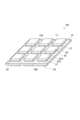
- FIG. 1 is a perspective view of a circuit board according to one embodiment.
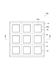
- FIG. 2 is a plan view of a circuit board according to one embodiment.
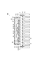
- FIG. 3 is a cross-sectional view taken along the line III--III of the circuit board of FIG.
- FIG. 4 is an enlarged cross-sectional view of a part of the cross-section of FIG. 3.
- FIG. 5 is a scanning electron microscope (SEM) photograph showing an example of a cross section along the thickness direction of the circuit board.
- FIG. 6 is a cross-sectional view of the power module.
- FIG. 7 is a scanning electron microscope (SEM) photograph showing a cross section along the thickness direction of the circuit board of Comparative Example 1.
- the numerical range indicated by "x to y” means greater than or equal to x and less than or equal to y.
- Numerical ranges in which the upper limit or lower limit of each numerical range in each embodiment is replaced with the numerical value of any example are also included in the present disclosure.
- a circuit board includes a ceramic plate, a metal plate, and a brazing material layer that joins the main surface of the ceramic plate and the main surface of the metal plate.
- the number of metal plates joined to one main surface of one ceramic plate may be one or multiple.
- the material of the ceramic plate is not particularly limited, and may be made of, for example, a nitride sintered body, a carbide sintered body, or an oxide sintered body. Specific examples include silicon nitride sintered bodies, aluminum nitride sintered bodies, aluminum oxide sintered bodies, and silicon carbide sintered bodies. There is no particular restriction as long as it is in the shape of a ceramic plate.
- the thickness of the ceramic plate may be, for example, 0.2 to 2 mm, or 0.32 to 1.1 mm.
- the metal plate may be a copper plate, for example.
- the shape of the metal plate is not particularly limited as long as a recess is formed along at least a part of the outer edge of the main surface opposite to the main surface of the ceramic plate.
- the thickness of the metal plate (distance between main surfaces) may be, for example, 0.1 to 1.2 mm, or 0.2 to 1.0 mm.
- the metal plate may have a plating film on its surface.
- the recess may be formed by a curved wall surface. That is, the metal plate may have an inner corner in the recess. This corner may extend parallel to the edge of the recess on the side surface of the metal plate.
- the brazing material layer may contain silver and copper, and may further contain one or more metals selected from the group consisting of tin and active metals. Two or more metals may be an alloy.
- the active metal may include one or more selected from the group consisting of titanium, hafnium, zirconium, and niobium.
- Silver and copper contained in the brazing material layer may be contained in the brazing material layer as an alloy such as an Ag--Cu eutectic alloy.
- the content of silver in the brazing material layer may be 45 to 95% by mass, or 50 to 95% by mass in terms of Ag.
- the total content of silver and copper in the brazing material layer may be 65 to 100% by mass, 70 to 99% by mass, or 90 to 98% by mass in terms of Ag and Cu, respectively. good. This makes it possible to sufficiently reduce the residual stress in the brazing material layer and improving the denseness of the brazing material layer.
- the content of the active metal in the brazing material layer may be 0.5 to 8 parts by mass based on 100 parts by mass of Ag and Cu in total.
- the content of the active metal may be 0.5 to 8 parts by mass based on 100 parts by mass of Ag and Cu in total.
- the metal contained in the brazing material layer may be contained as a nitride, oxide, carbide, or hydride.
- the braze layer may include titanium nitride and/or titanium hydride ( TiH2 ). This makes it possible to sufficiently increase the bonding strength between the ceramic plate and the metal plate.
- TiH 2 titanium nitride and/or titanium hydride
- the content of TiH 2 may be, for example, 1 to 8 parts by weight based on 100 parts by weight of Ag and Cu in total.
- FIG. 1 is a perspective view showing an example of a circuit board according to the present embodiment.
- 2 is a plan view of the circuit board of FIG. 1
- FIG. 3 is a sectional view taken along the line III--III of FIG.
- the circuit board 100 includes a ceramic plate 10 and a plurality of metal plates 20 on the main surface 10A and the main surface 10B of the ceramic board 10.
- the ceramic plate 10 has a flat plate shape.
- the ceramic plate 10 is divided into a plurality of sections by dividing lines on the main surface 10A.
- the principal surface 10A includes a plurality of partition lines L1 extending along a first direction and lined up at equal intervals, and a plurality of partition lines L1 extending along a second direction orthogonal to the first direction, as partition lines.
- a plurality of partition lines L2 arranged at equal intervals are provided.
- the partition line L1 and the partition line L2 are orthogonal to each other.
- the partition lines L1 and L2 may be formed by, for example, a plurality of recesses lined up in a straight line, or may have a linear groove formed therein. Specifically, it may be a scribe line formed with laser light. Examples of the laser source include a carbon dioxide laser and a YAG laser. A scribe line can be formed by intermittently irradiating laser light from such a laser source. Note that the partition lines L1 and L2 do not have to be arranged at equal intervals, and are not limited to being perpendicular to each other. Further, the partition lines L1 and L2 may not be straight, but may be curved or bent.
- the ceramic plate 10 has a plurality of partition areas 50 defined by partition lines L1 and L2.
- a metal plate 20 is provided in each of the plurality of divided areas 50.
- the plurality of metal plates 20 are independent from each other.
- the circuit board 100 is also called a collective board, and can be divided along partition lines L1 and L2. By dividing, a plurality of circuit boards (singulated boards) can be obtained. The individualized board obtained by dividing in this way is also an example of the circuit board of this embodiment.
- One main surface 20A of the metal plate 20 is exposed to the outside.
- the other main surface 20B of the metal plate 20 and the main surface 10A (main surface 10B) of the ceramic plate 10 are joined by a brazing material layer 30.
- a recess 22 is formed in the metal plate 20 along the outer edge of the main surface 20B (joint surface with the brazing material layer 30) of the metal plate 20.
- the metal plate 20 having such a recess 22 formed therein may be cut out so that the outer side of the main surface 20B has a step-like shape. As shown in FIG. 2, the recess 22 is formed all around the outer edge of the main surface 20B of the metal plate 20. That is, the outer edge of the main surface 20B is formed by the recess 22.
- the recess 22 may be provided only in the vicinity of the portion where the semiconductor element is soldered when the semiconductor element is mounted on the metal plate 20. Further, the recesses 22 may be provided only in some of the plurality of metal plates 20. For example, it is not necessary to provide the recess 22 in the metal plate 20 that serves as a heat sink of the power module.
- FIG. 4 shows a partially enlarged cross-section of the circuit board 100 shown in FIG. 3.
- 3 and 4 both show a cross section along the thickness direction of the metal plate 20, perpendicular to the edge 27 of the recess 22 on the side surface 20C of the metal plate 20.
- the width X of the recess 22 may be 0.05 mm or more, 0.2 mm or more, or 0.4 mm or more. In this way, as the width X increases, the distance from the brazing material layer 30 to the side surface 20C of the metal plate 20 increases. Therefore, creeping up of the brazing material onto the main surface 20A can be further suppressed.
- the width X may be 10 mm or less, 5 mm or less, 3 mm or less, 1.3 mm or less, or 1 mm or less.
- the ratio of the width X to the length of the main surface 20A of the metal plate 20 measured along the same direction as the width X may be 0.0005 to 0.5, and may be 0.001 to 0.3. It may be between 0.005 and 0.3.
- the length of the main surface 20A may be, for example, 5 to 100 mm, or 15 to 50 mm.
- the height Z of the recess 22 may be 0.05 mm or more, 0.2 mm or more, or 0.3 mm or more. In this way, as the height Z increases, the distance from the brazing material layer 30 to the side surface 20C of the metal plate 20 increases. Therefore, creeping up of the brazing material onto the main surface 20A of the metal plate 20 can be further suppressed.
- the height Z may be 1.1 mm or less, 0.6 mm or less, or 0.5 mm or less.
- the ratio of the height Z to the thickness of the metal plate 20 may be 0.04 to 1.0, or may be 0.1 to 0.6.
- the ratio of the height Z to the width X may be 0.001 to 22, and may be 0.1 to 4. It may be 0.15 to 3. Note that the width X is measured along a direction parallel to the main surfaces 10A and 10B of the ceramic plate 10 in the cross section shown in FIGS. 3 and 4. The height Z is measured along the direction perpendicular to the main surfaces 10A and 10B of the ceramic plate 10 in the cross section shown in FIGS. 3 and 4.
- the wall surface of the metal plate 20 constituting the recess 22 includes an opposing surface 24 that faces the main surfaces 10A and 10B of the ceramic plate 10, and an upright surface 23 that is orthogonal to the main surfaces 10A and 10B. At the boundary between the opposing surface 24 and the upright surface 23, an inside corner 25 extends parallel to the edge 27 of the recess 22. Since the metal plate 20 has the opposing surface 24 and the corner portion 25 in the recess 22, it is possible to further suppress the brazing material from creeping up from the brazing material layer 30.
- the upright surface 23 is perpendicular to the main surfaces 10A and 10B, but is not limited thereto.
- the facing surface 24 and/or the upright surface 23 may be inclined with respect to the main surface 10A and the main surface 10B.
- the width X and height Z are as shown in FIG.
- the width X and height Z are measured based on the most recessed part of the recess 22.
- the width X is measured based on the most outwardly protruding portion of the side surface 20C. That is, the width X can be determined as the maximum value of the distance between the side surface 20C and the wall surface constituting the recess, measured in a direction parallel to the main surface 20A in a cross section as shown in FIG.
- the height Z is the height between the main surface 10A (main surface 10B) and the wall surface (opposing surface 24) forming the recess 22, measured in a direction perpendicular to the main surface 20A in a cross section as shown in FIG. It can be determined as the maximum value of distance.
- FIG. 5 is a SEM photograph showing an example of a cross section along the thickness direction of the circuit board. Similar to FIG. 4, FIG. 5 shows a partially enlarged cross section of the side surface 20C of the metal plate 20, which is perpendicular to the edge 27 of the recess 22 and along the thickness direction of the metal plate 20.
- a rising portion 32 is formed at the end of the brazing material layer 30.
- the rising portion 32 has a substantially triangular shape below the inner corner portion 25 .
- the rising portion 32 has an inclined portion 32A that widens as it approaches the main surface 10A of the ceramic plate 10 inside the recessed portion 22. By having such an inclined portion 32A, creeping up of the brazing material onto the main surface 20A of the metal plate 20 can be further suppressed.
- the bonding area between the metal plate 20 and the ceramic plate 10 by the brazing material layer 30 can be increased, and the bonding strength can be increased.
- the size of the inclined portion 32A can be adjusted by changing the composition of the brazing material, the heating temperature and heating time during bonding, and the like.
- the metal plate 20 may function as a circuit board that has the function of transmitting electrical signals or a heat sink that has the function of transmitting heat. Further, the metal plate 20 may have both a function of transmitting heat and a function of transmitting an electric signal.
- the circuit board 100 and the individualized boards (circuit boards) obtained by dividing the same creeping up of the brazing material on the main surface 20A of the metal plate 20 on the side opposite to the ceramic plate side is suppressed. Therefore, it has excellent appearance and connection reliability with external circuits such as semiconductor elements. Therefore, it is suitable as a component mounted on a power module that requires high reliability.
- a power module includes a circuit board and a semiconductor element electrically connected to a metal plate of the circuit board.
- the circuit board may be the above-described circuit board 100 or a modification thereof, or may be another circuit board. The description regarding the circuit board 100 and its modifications is applied to the power module of this embodiment. Such a power module has excellent reliability.
- the circuit board and the semiconductor element may be sealed with resin.
- FIG. 6 is a cross-sectional view showing an example of the power module according to the present embodiment.
- the power module 300 includes a base plate 70 and a circuit board 101 joined to one side of the base plate 70 via solder 62.
- the metal plate 21 on one side of the circuit board 101 is joined to the base plate 70 via solder 62.
- a semiconductor element 60 is attached to at least one of the metal plates 20 on the other side of the circuit board 101 via solder 61.
- the semiconductor element 60 is connected to a predetermined location on the metal plate 20 with a metal wire 64 such as an aluminum wire. In this way, the semiconductor element 60 and the metal plate 20 are electrically connected.
- the metal plate 20a which is one of the metal plates 20, is connected to an electrode 63 provided through the casing 66 via a solder 65. ing.
- a housing 66 is disposed on one main surface of the base plate 70 and is integrated with the main surface to accommodate the circuit board 101.
- a housing space formed by one main surface of the base plate 70 and the housing 66 is filled with resin 80.
- the resin 80 seals the circuit board 101 and the semiconductor element 60.
- the resin may be, for example, a thermosetting resin or a photocuring resin.
- Cooling fins 72 forming a heat radiating section are joined to the other main surface of the base plate 70 via grease 74. Screws 73 are attached to the ends of the base plate 70 to fix the cooling fins 72 to the base plate 70.
- the base plate 70 and the cooling fins 72 may be made of aluminum.
- the base plate 70 and the cooling fins 72 have high thermal conductivity and function well as a heat dissipation section.
- the metal plate 20 and the metal plate 21 are electrically insulated by the ceramic plate 10.
- the metal plate 20 (20a) may form an electric circuit.
- the metal plate 20 and the metal plate 21 are respectively joined to the main surface 10A and the main surface 10B of the ceramic plate 10 by a brazing material layer (not shown).
- the metal plate 20 is formed with recesses as shown in FIGS. 1 to 5. This recess has the same size as the recess 22, and at least a portion of the wall surface of the metal plate 20 forming the recess may be covered with a brazing material layer. As a result, creeping up of the brazing material on the main surface of the metal plate 20 on which the semiconductor element 60 is mounted is sufficiently suppressed. Further, the recessed portion is sufficiently filled with resin 80. Therefore, the power module 300 has excellent electrical connection reliability between the semiconductor element 60 and the metal plate 20.
- the metal plate 21 may also have a recess 22 formed therein.
- a method for manufacturing a circuit board includes a preparation step of preparing one or more metal plates each having a recess formed along the outer edge of one main surface, and applying a brazing material to the main surface of the ceramic plate.
- a coating and drying process in which one or more coating layers are formed by coating and drying, and lamination in which a ceramic plate and one or more metal plates are laminated with one or more coating layers sandwiched therebetween to produce a laminate. and a joining step of heating the laminate to obtain a joined body in which a ceramic plate and one or more metal plates are joined with one or more brazing metal layers.
- the metal plate may be a copper plate, for example.
- the recessed portion can be formed, for example, by machining using a machining center.
- the size of the recess, ie width X and height Z, may be as described above.
- the recess may be formed in a part of the outer edge of the main surface of the metal plate, or may be formed by cutting the outer edge of the main surface of the metal plate over the entire circumference.
- the ceramic plate used in the coating and drying process can be produced, for example, by the following procedure.
- a green sheet is produced by molding a slurry containing an inorganic compound powder, a binder resin, a sintering aid, a plasticizer, a dispersant, a solvent, and the like.
- inorganic compounds include aluminum nitride (AlN), silicon nitride (Si 3 N 4 ), silicon carbide, and aluminum oxide.
- Sintering aids include rare earth metals, alkaline earth metals, metal oxides, fluorides, chlorides, nitrates, sulfates, and the like. These may be used alone or in combination of two or more.
- binder resins include methyl cellulose, ethyl cellulose, polyvinyl alcohol, polyvinyl butyral, and (meth)acrylic resins.
- plasticizers include purified glycerin, glycerin triolate, diethylene glycol, phthalic acid plasticizers such as di-n-butyl phthalate, and dibasic acid plasticizers such as di-2-ethylhexyl sebacate.
- dispersants include poly(meth)acrylates and (meth)acrylic acid-maleate copolymers.
- solvents include organic solvents such as ethanol and toluene.
- Examples of methods for forming green sheets include a doctor blade method and an extrusion method.
- the green sheet obtained by molding the slurry is degreased and sintered.
- Degreasing may be performed, for example, by heating at 400 to 800°C for 0.5 to 20 hours. Thereby, the amount of residual organic matter (carbon) can be reduced while suppressing oxidation and deterioration of inorganic compounds.
- Sintering is performed by heating to 1700 to 1900° C. in a non-oxidizing gas atmosphere such as nitrogen, argon, ammonia, or hydrogen. In this way, for example, a ceramic plate 10 can be obtained. If necessary, the ceramic plate may be laser-processed to cut the edges or provide scribe lines.
- the above-mentioned degreasing and sintering may be performed, for example, with a plurality of green sheets laminated.
- a release layer made of a release agent may be provided between the green sheets to facilitate separation of the base materials after sintering.
- the mold release agent for example, boron nitride (BN) can be used.
- the release layer may be formed, for example, by applying a slurry of boron nitride powder by spraying, brushing, roll coating, screen printing, or the like.
- the number of green sheets to be laminated may be, for example, 8 to 100, or 30 to 70, from the viewpoint of efficient mass production of ceramic plates and sufficient degreasing.
- a partition line may be formed on the one main surface.
- a scribe line may be provided as a partition line by irradiating the main surface of the ceramic plate with a laser beam.
- the laser beam irradiated onto the main surface of the ceramic include a carbon dioxide laser and a YAG laser.
- scribe lines that become the partition lines L1 and L2 as shown in FIGS. 1 and 2 are formed.
- Such partition lines L1 and L2 can be used as cutting lines when dividing the circuit board in a subsequent process.
- the brazing material applied to the main surface of the ceramic plate contains, for example, silver, copper, tin, active metals, metal compounds containing these as constituent elements, organic solvents, binders, and the like.
- the viscosity of the brazing filler metal may be, for example, 5 to 20 Pa ⁇ s.
- the organic solvent content in the brazing filler metal may be, for example, 5 to 25% by mass, and the binder content may be, for example, 2 to 15% by mass.
- the brazing filler metal may contain silver in the form of a single metal or a metal compound (alloy), and in addition to silver, it may contain one or more metals selected from the group consisting of copper, tin, and active metals. It's fine. Two or more metals may be an alloy.
- the active metal may include one or more selected from the group consisting of titanium, hafnium, zirconium, and niobium.
- the content of silver in the brazing filler metal may be 45 to 95% by mass, or 50 to 95% by mass in terms of Ag.
- the total content of silver and copper in the brazing material may be 65 to 100% by mass, 70 to 99% by mass, or 90 to 98% by mass in terms of Ag and Cu, respectively. . This makes it possible to sufficiently reduce the residual stress in the brazing material layer formed in a subsequent process and improving the density of the brazing material layer.
- the content of active metal in the brazing material may be 0.5 to 8 parts by mass based on 100 parts by mass of Ag and Cu in total.
- the content of the active metal may be 0.5 to 8 parts by mass based on 100 parts by mass of Ag and Cu in total.
- the metal contained in the brazing filler metal may be contained as a nitride, oxide, carbide, or hydride.
- the brazing material may include titanium nitride and/or titanium hydride ( TiH2 ). This makes it possible to sufficiently increase the bonding strength between the ceramic plate and the metal plate.
- TiH 2 titanium nitride and/or titanium hydride
- the content of TiH 2 may be, for example, 1 to 8 parts by weight based on 100 parts by weight of Ag and Cu in total.
- the content of tin in the brazing filler metal may be 0.5 to 5 parts by mass based on 100 parts by mass of Ag and Cu in total.
- the tin content may be 0.5 to 5 parts by mass based on 100 parts by mass of Ag and Cu in total.
- One or more coating layers are provided on the main surface of the ceramic plate by applying and drying a brazing material by a method such as a roll coater method, screen printing method, or transfer method.
- the coating layer may be provided at a position where the metal plates are to be joined. Therefore, the number of coated layers may be the same as the number of metal plates bonded to the ceramic plate.
- the coating layer is formed, a ceramic plate and a metal plate are laminated with the coating layer sandwiched between them to produce a laminate.
- the two main surfaces of the metal plates are stacked such that the main surface on which the recess is formed faces the main surface of the ceramic plate.
- the metal plate may be pressed in the direction toward the ceramic plate. As the pressure is applied, the coating layer spreads, and a laminate in which the ceramic plate and the metal plate are well bonded by the coating layer is obtained.
- each of the plurality of metal plates 20 is arranged independently for each partition area 50 defined by partition lines L1 and L2 on the main surface 10A of the ceramic plate 10.
- a plurality of metal plates 20 are laminated to produce a laminate.
- the obtained laminate is heated in a heating furnace to obtain a joined body in which the ceramic plate and the metal plate are joined with a brazing material layer.
- the heating temperature may be, for example, 700 to 900°C.
- the atmosphere in the furnace may be an inert gas such as nitrogen, and the reaction may be performed under reduced pressure below atmospheric pressure or under vacuum.
- the heating furnace may be of a continuous type that continuously manufactures a plurality of joined bodies, or may be one that manufactures one or more joined bodies in a batch manner. Heating may be performed while pressing the joined body in the stacking direction of the laminate.
- the brazing material contained in the coating layer flows and reacts with the metal plate, forming a brazing material layer.
- the brazing material layer may include a reaction product between the brazing material and a metal component contained in the metal plate.
- a portion of the brazing material may climb up the wall surface of the metal plate constituting the recess, forming a climbing portion 32 as shown in FIG.
- surface treatment such as forming a plating film on the metal plate is performed.
- cutting or the like may be performed to adjust the shape of the brazing material layer. In this way, a circuit board can be manufactured.
- a dividing step may be performed in which the aggregate substrate is divided into individual pieces. .
- the collective board can be divided along the division lines L1 and L2 to obtain a plurality of circuit boards.
- a joined body can be obtained by joining a plurality of metal plates that have been previously processed to a predetermined size.
- a circuit board in which creeping up is suppressed can be efficiently manufactured without performing a resist printing process and a metal plate etching process.
- the circuit board obtained by such a manufacturing method can reduce manufacturing costs and has excellent appearance and connection reliability with external circuits such as semiconductor elements.
- the manufacturing method of the circuit boards 100, 101 and their modifications described above is not limited to the manufacturing method described above.
- a power module may be manufactured using the circuit board obtained in this way.
- a power module can be manufactured by mounting a semiconductor element on a circuit board using solder and wire bonding, etc., housing the circuit board and semiconductor element in a housing space of a housing, and then sealing it with resin. .
- a plurality of metal plates are provided on each of the pair of main surfaces of the ceramic plate, but the present invention is not limited thereto.
- one or more metal plates may be provided on only one main surface of the ceramic plate.
- the structure and shape of the brazing material layer and the metal plate provided on each of the pair of main surfaces of the ceramic plate may be different from each other.
- one metal plate may be provided on each of the pair of main surfaces of the ceramic plate.
- the recess does not need to be provided so as to surround the main surface.
- a circuit board comprising a ceramic plate, a metal plate, and a brazing material layer that joins the main surface of the ceramic plate and the main surface of the metal plate, A circuit board, wherein a recess is formed in the metal plate along at least a part of an outer edge of the main surface of the metal plate.
- a circuit board wherein the recess in the metal plate is formed all around the outer edge of the main surface of the metal plate.
- the wall surface of the metal plate forming the recess includes a facing surface facing the main surface of the ceramic plate.
- Substrate manufacturing method [8]
- a plurality of metal plates in which the recesses are formed are prepared
- the laminated body is produced by laminating the plurality of metal plates such that each of the plurality of metal plates is independent for each partition area defined by a partition line on the main surface of the ceramic plate.
- a power module comprising: a semiconductor element electrically connected to the semiconductor element;
- a brazing filler metal containing Ag, Cu, Sn, and TiH2 was prepared.
- the mass ratio of Ag to Cu in the brazing filler metal was 9:1.
- This brazing filler metal contained 3 parts by mass of Sn and 3.5 parts by mass of TiH 2 based on 100 parts by mass of Ag and Cu in total.
- the main surface of the ceramic plate was divided into 24 divided areas by scribe lines.
- a brazing material was applied to each section by screen printing to form a coating layer.
- the coating area of the coating layer was the same as the area of the main surface of the copper plate to be bonded to the ceramic plate.
- a copper plate was laminated on the ceramic plate so that the coating layer and the main surface of the copper plate were in contact with each other. In this way, a total of 24 copper plates were laminated on one main surface of the ceramic plate so that each section was independent.
- FIG. 5 is a SEM photograph of a cross section of the circuit board of Example 1. The measurement results were as shown in Table 1. The measurements were performed on only one circuit board. Note that all 24 copper plates were processed under the same machining conditions. Therefore, the values of the width X and height Z of the recess can be considered to be the same.
- the ceramic circuit board was cut perpendicular to the edge of the recess on the side surface of the metal plate and along the thickness direction of the copper plate.
- the obtained cut surface was confirmed with a microscope (magnification: 250 times) to evaluate the ability to fill the recesses of the copper plate with the resin.
- the case where the entire recess was filled with resin was rated "A"
- the case where only a part of the recess was filled with resin was rated "B".
- Example 2 The procedure was the same as in Example 1, except that the amount of cutting of the outer edge on one main surface of the copper plate by machining was changed, and the width X and height Z of the recess in the copper plate were changed as shown in Table 1. A circuit board was created. Then, the circuit board was evaluated in the same manner as in Example 1. The evaluation results were as shown in Table 1.
- FIG. 7 is an SEM photograph of a cross section of the circuit board of Comparative Example 1. As shown in FIG. 7, the copper plate 120 and the ceramic plate 110 were joined via the brazing material layer 130. The brazing material had even reached the main surface on the opposite side from the ceramic plate 110 side.
- SYMBOLS 10 110... Ceramic plate, 10A, 10B... Main surface, 20, 20a... Metal plate, 20A... Main surface, 20B... Main surface, 20C... Side surface, 22... Recessed part, 23... Standing surface, 24... Opposing surface, 25... Inner corner, 27... Edge, 30, 130... Brazing material layer, 32... Rising portion, 32A... Inclined portion, 50... Division area, 60... Semiconductor element, 61, 62, 65... Solder, 63... Electrode, 64... Metal wire, 66... Housing, 70... Base plate, 72... Cooling fin, 73... Screw, 74... Grease, 80... Resin, 100, 101... Circuit board, 110... Ceramic board, 120... Copper plate, 300...power module, L1, L2...compartment line.
Abstract
Provided is a printed circuit board comprising a ceramic plate, a metal plate, and a brazing layer joining a main surface of the ceramic plate and a main surface of the metal plate, wherein recesses are formed in the metal plate along at least a portion of the outer edge of the main surface of the metal plate. Also provided is a power module comprising the printed circuit board and semiconductor elements electrically connected to the metal plate of the printed circuit board.
Description
本開示は、回路基板及びその製造方法、並びにパワーモジュールに関する。
The present disclosure relates to a circuit board, a method for manufacturing the same, and a power module.
ロボット及びモーター等の産業機器の高性能化に伴い、大電流及び高電圧を制御するパワーモジュールが使用されている。このようなパワーモジュールに備えられる回路基板は、セラミック基板と銅板と備えており、これらは活性金属を含有するろう材を介して接合される。このような回路基板を形成する際に、ろう材が銅板の表面に染み出して銅板の側面を伝って這い上がる現象が生じる。このような現象が生じると、外観を損なうだけではなく、例えば半導体素子を接合する際に用いるはんだ材のぬれ製の悪化につながることも懸念される。
With the increasing performance of industrial equipment such as robots and motors, power modules that control large currents and high voltages are being used. A circuit board included in such a power module includes a ceramic substrate and a copper plate, which are joined via a brazing material containing an active metal. When forming such a circuit board, a phenomenon occurs in which the brazing material seeps onto the surface of the copper plate and creeps up along the side surface of the copper plate. If such a phenomenon occurs, it is feared that it will not only impair the appearance, but also lead to deterioration in the wettability of the solder material used, for example, when bonding semiconductor elements.
特許文献1では、ろう材の這い上がりを抑制するため、金属板の側面に表面粗さの大きい粗部を設けることが提案されている。特許文献2では、這い上がり現象によるシミの発生を抑制するため、半導体素子が搭載される搭載予定面を囲むように回路層にリブを設ける技術が提案されている。特許文献3では、金属板のうち、バリが生じている側の表面をセラミック板の一方の面に重ねるようにして積層してろう付けすることが提案されている。このような技術によって、ろう材の這い上がりによって生じるシミの問題を解決することが試みられている。
Patent Document 1 proposes providing a rough portion with a large surface roughness on the side surface of a metal plate in order to suppress creeping up of the brazing material. Patent Document 2 proposes a technique in which a rib is provided in a circuit layer so as to surround a mounting surface on which a semiconductor element is to be mounted, in order to suppress the occurrence of stains due to the creeping phenomenon. Patent Document 3 proposes laminating and brazing the metal plates so that the surface on the side where burrs are formed overlaps one surface of the ceramic plate. Using such techniques, attempts have been made to solve the problem of stains caused by creeping up of the brazing filler metal.
多数個取りの回路基板の製造方法としては、エッチング法が知られている。エッチング法では、金属板を所定のサイズに加工するためにレジスト印刷及びエッチングの工程が必要となる。一方、予め所定のサイズに加工された金属板を接合する搭載法であれば、このような工程が不要となり、生産効率を向上することができる。このような搭載法の場合、金属板の端部とセラミック板との接合信頼性を確保するために、ろう材の塗布量を十分に確保する必要がある。ところが、ろう材の塗布量が多くなると、ろう材の這い上がりが生じることが懸念される。そこで、本開示は、ろう材の這い上がりを抑制することが可能な回路基板及びその製造方法を提供する。また、本開示は、そのような回路基板を備えるパワーモジュールを提供する。
An etching method is known as a method for manufacturing multi-chip circuit boards. The etching method requires resist printing and etching steps to process the metal plate into a predetermined size. On the other hand, if a mounting method is used in which metal plates that have been pre-processed to a predetermined size are joined together, such a process is not necessary, and production efficiency can be improved. In the case of such a mounting method, it is necessary to ensure a sufficient amount of brazing material to be applied in order to ensure bonding reliability between the end of the metal plate and the ceramic plate. However, if the amount of brazing filler metal applied is large, there is a concern that the brazing filler metal may creep up. Therefore, the present disclosure provides a circuit board and a method for manufacturing the same that can suppress creeping up of the brazing material. The present disclosure also provides a power module including such a circuit board.
本開示の一側面に係る回路基板は、セラミック板と、金属板と、セラミック板の主面と金属板の主面とを接合するろう材層と、を備える回路基板であって、金属板の主面の外縁の少なくとも一部に沿って凹部が形成されている。
A circuit board according to one aspect of the present disclosure is a circuit board including a ceramic plate, a metal plate, and a brazing material layer that joins the main surface of the ceramic plate and the main surface of the metal plate, the circuit board comprising: A recess is formed along at least a portion of the outer edge of the main surface.
上記回路基板では、金属板の主面の外縁の少なくとも一部に沿って金属板に凹部が形成されているため、ろう材が、金属板を這い上がり、金属板のセラミック板側とは反対側の主面にろう材が到達することを十分に抑制できる。このようにろう材の這い上がりが抑制された回路基板は、外観及び半導体素子等の外部回路との接続信頼性に優れる。
In the above circuit board, the metal plate has a recess formed along at least a part of the outer edge of the main surface of the metal plate, so that the brazing material creeps up the metal plate and reaches the opposite side of the metal plate from the ceramic plate side. It is possible to sufficiently prevent the brazing filler metal from reaching the main surface. A circuit board in which creeping up of the brazing material is suppressed in this manner has excellent appearance and connection reliability with external circuits such as semiconductor elements.
上記金属板における凹部は、金属板の主面の外縁の全周にわたって形成されていてよい。これによって、ろう材層から金属板のセラミック板側とは反対側の主面にろう材が這い上がることを一層抑制することができる。
The recess in the metal plate may be formed all around the outer edge of the main surface of the metal plate. Thereby, it is possible to further suppress the brazing material from creeping up from the brazing material layer to the main surface of the metal plate on the side opposite to the ceramic plate side.
上記凹部を構成する金属板の壁面は、セラミック板の主面と対向する対向面を含んでよい。凹部を構成する金属板の壁面がこのような対向面を有することによって、ろう材の這い上がりを一層抑制することができる。
The wall surface of the metal plate constituting the recess may include an opposing surface that faces the main surface of the ceramic plate. By having the wall surface of the metal plate constituting the recessed portion having such a facing surface, creeping up of the brazing material can be further suppressed.
上記回路基板を、金属板の側面における凹部の端縁に直交し、金属板の厚さ方向に沿う断面で見たときに、凹部の幅Xは0.05mm以上であってよく、凹部の高さZは0.05mm以上であってよい。凹部がこのようなサイズを有することによって、ろう材の這い上がりを一層抑制することができる。
When the circuit board is viewed in a cross section perpendicular to the edge of the recess on the side surface of the metal plate and along the thickness direction of the metal plate, the width X of the recess may be 0.05 mm or more, and the height of the recess may be The length Z may be 0.05 mm or more. When the recess has such a size, creeping up of the brazing material can be further suppressed.
上記回路基板を、金属板の側面における凹部の端縁に直交し、金属板の厚さ方向に沿う断面で見たときに、ろう材層は、凹部内においてセラミック板の主面に近づくにつれて拡がる傾斜部を有してよい。ろう材層がこのような傾斜部を有することによって、ろう材の這い上がりを一層抑制することができる。また、ろう材層とセラミック板の主面との接合面積を大きくして、接合信頼性を向上することができる。
When the above circuit board is viewed in a cross section along the thickness direction of the metal plate and perpendicular to the edge of the recess on the side surface of the metal plate, the brazing filler metal layer spreads within the recess as it approaches the main surface of the ceramic plate. It may have an inclined portion. When the brazing material layer has such an inclined portion, creeping up of the brazing material can be further suppressed. Furthermore, the bonding area between the brazing filler metal layer and the main surface of the ceramic plate can be increased to improve bonding reliability.
上記回路基板は、セラミック板と、複数の金属板と、セラミック板の上記主面と複数の金属板の主面のそれぞれとを接合する複数のろう材層と、を備え、複数の金属板が、凹部が形成されている上記金属板を含んでよい。
The circuit board includes a ceramic plate, a plurality of metal plates, and a plurality of brazing metal layers bonding the main surface of the ceramic plate and each of the main surfaces of the plurality of metal plates, and the plurality of metal plates , the metal plate may include the metal plate in which a recess is formed.
上記回路基板では、少なくとも一つの金属板の主面の外縁に沿って金属板に凹部が形成されているため、ろう材が、当該金属板の側面を這い上がり、金属板のセラミック板側とは反対側の主面にろう材が到達することを十分に抑制できる。このようにろう材の這い上がりが抑制された回路基板は、外観及び半導体素子との接続信頼性に優れる。なお、複数の金属板のそれぞれは、セラミック板の主面における区画線で画定される区画領域毎に独立して設けられてよい。このような回路基板は、多数個取り回路基板であってよい。このような多数個取り回路基板を分割すれば、複数の個片化基板(分割基板)を纏めて製造することができる。このような回路基板は、生産効率に優れる。
In the circuit board described above, since a recess is formed in the metal plate along the outer edge of the main surface of at least one metal plate, the brazing filler metal creeps up the side of the metal plate and is separated from the ceramic plate side of the metal plate. It is possible to sufficiently prevent the brazing filler metal from reaching the main surface on the opposite side. A circuit board in which creeping up of the brazing material is suppressed in this manner has excellent appearance and connection reliability with semiconductor elements. Note that each of the plurality of metal plates may be provided independently for each partition area defined by a partition line on the main surface of the ceramic plate. Such a circuit board may be a multi-chip circuit board. By dividing such a multi-chip circuit board, a plurality of individualized boards (divided boards) can be manufactured at once. Such a circuit board has excellent production efficiency.
本開示の一側面に係る回路基板の製造方法は、一方の主面の外縁の少なくとも一部に沿って凹部が形成されている一つ又は複数の金属板を準備する準備工程と、セラミック板の主面にろう材を塗布及び乾燥して一つ又は複数の塗布層を設ける塗布乾燥工程と、一つ又は複数の塗布層を挟むようにしてセラミック板と一つ又は複数の金属板とを積層して積層体を作製する積層工程と、積層体を加熱してセラミック板と一つ又は複数の金属板とが一つ又は複数のろう材層で接合された接合体を得る接合工程と、を有し、積層工程において、一つ又は複数の金属板の一方の主面とセラミック板の主面とが対向するようにセラミック板と一つ又は複数の金属板とを積層する。
A method for manufacturing a circuit board according to one aspect of the present disclosure includes a preparation step of preparing one or more metal plates each having a recess formed along at least a part of the outer edge of one main surface; A coating and drying process in which one or more coating layers are formed by applying and drying a brazing filler metal on the main surface, and a ceramic plate and one or more metal plates are laminated with one or more coating layers in between. The method includes a lamination step of producing a laminate, and a joining step of heating the laminate to obtain a joined body in which a ceramic plate and one or more metal plates are joined with one or more brazing metal layers. In the lamination step, the ceramic plate and the one or more metal plates are laminated so that one main surface of the one or more metal plates faces the main surface of the ceramic plate.
上記製造方法では、積層工程で、一つ又は複数の金属板の主面のうち凹部が形成されている方の主面と金属板とが対向するようにセラミック板と一つ又は複数の金属板とを積層している。このようにして得られる積層体を用いて接合工程を行っているため、ろう材が金属板の側面を這い上がり、金属板のセラミック板側とは反対側の主面にろう材が到達することを十分に抑制できる。このようにろう材の這い上がりが抑制された回路基板は、外観及び半導体素子等の外部回路との接続信頼性に優れる。
In the above manufacturing method, in the lamination process, the ceramic plate and the one or more metal plates are stacked so that the main surface of the one or more metal plates, on which the concave portion is formed, faces the metal plate. are laminated. Because the bonding process is carried out using the laminate obtained in this way, the brazing metal creeps up the side of the metal plate and reaches the main surface of the metal plate on the opposite side from the ceramic plate side. can be sufficiently suppressed. A circuit board in which creeping up of the brazing material is suppressed in this manner has excellent appearance and connection reliability with external circuits such as semiconductor elements.
上記製造方法の準備工程では凹部が形成されている複数の金属板を準備し、積層工程では、複数の金属板のそれぞれが、セラミック板の主面における区画線で画定される区画領域毎に独立するように複数の金属板を積層して積層体を作製し、接合工程の後に、接合体におけるセラミック板を区画線に沿って分割する分割工程を有してよい。
In the preparation step of the above manufacturing method, a plurality of metal plates in which recesses are formed are prepared, and in the lamination step, each of the plurality of metal plates is separated into separate areas defined by partition lines on the main surface of the ceramic plate. A laminate may be produced by laminating a plurality of metal plates as shown in FIG.
このような接合工程で得られる接合体は、多数個取り回路基板ということもできる。分割工程において、このような多数個取り回路基板を分割すれば、複数の個片化基板(分割基板)を纏めて製造することができる。このような製造方法は、高い生産効率で回路基板(個片化基板)を製造することができる。
The bonded body obtained by such a bonding process can also be called a multi-chip circuit board. In the dividing step, by dividing such a multi-chip circuit board, a plurality of individualized boards (divided boards) can be manufactured all at once. Such a manufacturing method can manufacture circuit boards (singulated boards) with high production efficiency.
本開示の一側面に係るパワーモジュールは、上述のいずれかの回路基板と、当該回路基板の金属板に電気的に接続される半導体素子と、を備える。このようなパワーモジュールは、上述のいずれかの回路基板を備えることから信頼性に優れる。
A power module according to one aspect of the present disclosure includes any of the circuit boards described above and a semiconductor element electrically connected to the metal plate of the circuit board. Such a power module has excellent reliability because it includes any of the above-mentioned circuit boards.
ろう材の這い上がりを抑制することが可能な回路基板及びその製造方法を提供することができる。また、そのような回路基板を備えるパワーモジュールを提供することができる。
It is possible to provide a circuit board that can suppress brazing filler metal from creeping up, and a method for manufacturing the same. Furthermore, a power module including such a circuit board can be provided.
以下、場合により図面を参照して、本開示の実施形態を説明する。ただし、以下の実施形態は、本開示を説明するための例示であり、本開示を以下の内容に限定する趣旨ではない。説明において、同一要素又は同一機能を有する要素には同一符号を用い、場合により重複する説明は省略する。また、上下左右等の位置関係は、特に断らない限り、図面に示す位置関係に基づくものとする。更に、各要素の寸法比率は図示の比率に限られるものではない。なお、「~」の記号で示される数値範囲は、下限値及び上限値を含む。すなわち、「x~y」で示される数値範囲は、x以上且つy以下を意味する。各実施形態における各数値範囲の上限又は下限をいずれかの実施例の数値で置き換えた数値範囲も本開示に含まれる。
Hereinafter, embodiments of the present disclosure will be described with reference to the drawings as the case may be. However, the following embodiments are examples for explaining the present disclosure, and are not intended to limit the present disclosure to the following contents. In the description, the same reference numerals will be used for the same elements or elements having the same function, and redundant description will be omitted in some cases. In addition, the positional relationships such as top, bottom, left, and right are based on the positional relationships shown in the drawings unless otherwise specified. Furthermore, the dimensional ratio of each element is not limited to the ratio shown in the drawings. Note that the numerical range indicated by the symbol "~" includes a lower limit value and an upper limit value. That is, the numerical range indicated by "x to y" means greater than or equal to x and less than or equal to y. Numerical ranges in which the upper limit or lower limit of each numerical range in each embodiment is replaced with the numerical value of any example are also included in the present disclosure.
一実施形態に係る回路基板は、セラミック板と、金属板と、セラミック板の主面と金属板の主面とを接合するろう材層と、を備える。一枚のセラミック板の一方の主面に接合される金属板は、一つであってもよいし、複数であってもよい。セラミック板の材質は特に制限されず、例えば、窒化物焼結体、炭化物焼結体、又は酸化物焼結体で構成されていてよい。具体的には、窒化ケイ素焼結体、窒化アルミニウム焼結体、酸化アルミニウム焼結体、及び炭化ケイ素焼結体等が挙げられる。セラミック板の板状であれば特に制限されない。セラミック板の厚みは、例えば0.2~2mmであってよく、0.32~1.1mmであってもよい。
A circuit board according to one embodiment includes a ceramic plate, a metal plate, and a brazing material layer that joins the main surface of the ceramic plate and the main surface of the metal plate. The number of metal plates joined to one main surface of one ceramic plate may be one or multiple. The material of the ceramic plate is not particularly limited, and may be made of, for example, a nitride sintered body, a carbide sintered body, or an oxide sintered body. Specific examples include silicon nitride sintered bodies, aluminum nitride sintered bodies, aluminum oxide sintered bodies, and silicon carbide sintered bodies. There is no particular restriction as long as it is in the shape of a ceramic plate. The thickness of the ceramic plate may be, for example, 0.2 to 2 mm, or 0.32 to 1.1 mm.
金属板は、例えば銅板であってよい。金属板の形状は、セラミック板の主面に対向する主面の外縁の少なくとも一部に沿って凹部が形成されていれば特に制限されない。金属板の厚み(主面間の距離)は、例えば0.1~1.2mmであってよく、0.2~1.0mmであってもよい。金属板は表面にめっき膜を有していてもよい。凹部は屈曲した壁面によって構成されていてよい。すなわち、金属板は、凹部に入隅部を有してよい。この入隅部は、金属板の側面における凹部の端縁と平行に延びていてよい。金属板がこのような凹部を備えることによって、ろう材が金属板のセラミック板側とは反対側の主面に這い上がることを十分に抑制することができる。
The metal plate may be a copper plate, for example. The shape of the metal plate is not particularly limited as long as a recess is formed along at least a part of the outer edge of the main surface opposite to the main surface of the ceramic plate. The thickness of the metal plate (distance between main surfaces) may be, for example, 0.1 to 1.2 mm, or 0.2 to 1.0 mm. The metal plate may have a plating film on its surface. The recess may be formed by a curved wall surface. That is, the metal plate may have an inner corner in the recess. This corner may extend parallel to the edge of the recess on the side surface of the metal plate. By providing the metal plate with such a recessed portion, it is possible to sufficiently suppress the brazing material from creeping up to the main surface of the metal plate on the side opposite to the ceramic plate side.
ろう材層は、銀及び銅を含んでよく、さらに、錫、及び活性金属からなる群より選ばれる一種又は二種以上の金属を含有してよい。二種以上の金属は合金となっていてもよい。活性金属は、チタン、ハフニウム、ジルコニウム、及びニオブからなる群より選ばれる一種又は二種以上を含んでいてよい。ろう材層に含まれる銀及び銅は、例えばAg-Cu共晶合金等の合金としてろう材層に含まれていてもよい。ろう材層における銀の含有量は、Ag換算で45~95質量%であってよく、50~95質量%であってもよい。ろう材層における銀及び銅の合計含有量は、それぞれAg及びCuに換算して65~100質量%であってよく、70~99質量%であってよく、90~98質量%であってもよい。これによって、ろう材層における残留応力を十分に低減しつつ、ろう材層の緻密性を向上することができる。
The brazing material layer may contain silver and copper, and may further contain one or more metals selected from the group consisting of tin and active metals. Two or more metals may be an alloy. The active metal may include one or more selected from the group consisting of titanium, hafnium, zirconium, and niobium. Silver and copper contained in the brazing material layer may be contained in the brazing material layer as an alloy such as an Ag--Cu eutectic alloy. The content of silver in the brazing material layer may be 45 to 95% by mass, or 50 to 95% by mass in terms of Ag. The total content of silver and copper in the brazing material layer may be 65 to 100% by mass, 70 to 99% by mass, or 90 to 98% by mass in terms of Ag and Cu, respectively. good. This makes it possible to sufficiently reduce the residual stress in the brazing material layer and improving the denseness of the brazing material layer.
ろう材層における活性金属の含有量は、Ag及びCuの合計100質量部に対して、0.5~8質量部であってよい。活性金属の含有量を0.5質量部以上とすることで、セラミック板とろう材層との接合性を向上することができる。一方、活性金属の含有量を8質量部以下とすることで、接合界面に脆弱な合金層が形成されることを抑制できる。
The content of the active metal in the brazing material layer may be 0.5 to 8 parts by mass based on 100 parts by mass of Ag and Cu in total. By setting the content of the active metal to 0.5 parts by mass or more, the bondability between the ceramic plate and the brazing material layer can be improved. On the other hand, by setting the content of the active metal to 8 parts by mass or less, formation of a fragile alloy layer at the bonding interface can be suppressed.
ろう材層に含有される上記金属は、窒化物、酸化物、炭化物又は水素化物として含まれていてもよい。一例として、ろう材層は、窒化チタン及び/又は水素化チタン(TiH2)を含んでいてよい。これによって、セラミック板と金属板との接合強度を十分に高くすることができる。AgとCuの合計100質量部に対するTiH2の含有量は例えば1~8質量部であってよい。
The metal contained in the brazing material layer may be contained as a nitride, oxide, carbide, or hydride. As an example, the braze layer may include titanium nitride and/or titanium hydride ( TiH2 ). This makes it possible to sufficiently increase the bonding strength between the ceramic plate and the metal plate. The content of TiH 2 may be, for example, 1 to 8 parts by weight based on 100 parts by weight of Ag and Cu in total.
図1は、本実施形態に係る回路基板の一例を示す斜視図である。図2は、図1の回路基板の平面図であり、図3は、図2のIII-III線断面図である。図1、図2及び図3に示すように、回路基板100は、セラミック板10と、セラミック板10の主面10A及び主面10B上に複数の金属板20と、を備える。
FIG. 1 is a perspective view showing an example of a circuit board according to the present embodiment. 2 is a plan view of the circuit board of FIG. 1, and FIG. 3 is a sectional view taken along the line III--III of FIG. As shown in FIGS. 1, 2, and 3, the circuit board 100 includes a ceramic plate 10 and a plurality of metal plates 20 on the main surface 10A and the main surface 10B of the ceramic board 10.
セラミック板10は、平板形状を有する。セラミック板10は主面10Aにおける区画線によって複数に区画されている。主面10Aには、区画線として、第1の方向に沿って延在し且つ等間隔で並ぶ複数の区画線L1と、第1の方向に直交する第2の方向に沿って延在し且つ等間隔で並ぶ複数の区画線L2と、が設けられている。区画線L1と区画線L2とは互いに直交している。
The ceramic plate 10 has a flat plate shape. The ceramic plate 10 is divided into a plurality of sections by dividing lines on the main surface 10A. The principal surface 10A includes a plurality of partition lines L1 extending along a first direction and lined up at equal intervals, and a plurality of partition lines L1 extending along a second direction orthogonal to the first direction, as partition lines. A plurality of partition lines L2 arranged at equal intervals are provided. The partition line L1 and the partition line L2 are orthogonal to each other.
区画線L1,L2は、例えば、複数の凹みが直線状に並んで構成されていてもよいし、線状に溝が形成されていてもよい。具体的には、レーザー光で形成されるスクライブラインであってよい。レーザー源としては、例えば、炭酸ガスレーザー及びYAGレーザー等が挙げられる。このようなレーザー源からレーザー光を間欠的に照射することによってスクライブラインを形成することができる。なお、区画線L1,L2は、等間隔で並んでいなくてもよく、また、直交するものに限定されない。また、区画線L1,L2は、直線状ではなく、曲線状であってもよいし、折れ曲がっていてもよい。
The partition lines L1 and L2 may be formed by, for example, a plurality of recesses lined up in a straight line, or may have a linear groove formed therein. Specifically, it may be a scribe line formed with laser light. Examples of the laser source include a carbon dioxide laser and a YAG laser. A scribe line can be formed by intermittently irradiating laser light from such a laser source. Note that the partition lines L1 and L2 do not have to be arranged at equal intervals, and are not limited to being perpendicular to each other. Further, the partition lines L1 and L2 may not be straight, but may be curved or bent.
セラミック板10は、区画線L1及び区画線L2によって画定される複数の区画領域50を有する。複数の区画領域50のそれぞれに、金属板20が設けられている。複数の金属板20は、それぞれ互いに独立している。回路基板100は、集合基板とも称されるものであり、区画線L1,L2に沿って分割することができる。分割することによって複数の回路基板(個片化基板)を得ることができる。このように分割して得られる個片化基板も、本実施形態の回路基板の一例である。
The ceramic plate 10 has a plurality of partition areas 50 defined by partition lines L1 and L2. A metal plate 20 is provided in each of the plurality of divided areas 50. The plurality of metal plates 20 are independent from each other. The circuit board 100 is also called a collective board, and can be divided along partition lines L1 and L2. By dividing, a plurality of circuit boards (singulated boards) can be obtained. The individualized board obtained by dividing in this way is also an example of the circuit board of this embodiment.
金属板20の一方の主面20Aは外部に露出している。金属板20の他方の主面20Bとセラミック板10の主面10A(主面10B)は、ろう材層30によって接合されている。金属板20の主面20B(ろう材層30との接合面)の外縁に沿って、金属板20には凹部22が形成されている。このような凹部22が形成された金属板20は、主面20Bの外側が階段状になるように切り欠かれたものであってよい。図2に示されるように、凹部22は、金属板20の主面20Bにおける外縁の全周にわたって形成されている。すなわち、主面20Bの外縁は凹部22で形成されている。ただし、凹部22を主面20Bの外縁の全周にわたって設けることは必須ではない。変形例では、金属板20の上に半導体素子が搭載される際に半田付けがなされる部分の近傍のみに、凹部22を設けてもよい。また、複数の金属板20の一部のみに凹部22を設けてもよい。例えば、パワーモジュールの放熱板となる金属板20には凹部22を設けなくてもよい。
One main surface 20A of the metal plate 20 is exposed to the outside. The other main surface 20B of the metal plate 20 and the main surface 10A (main surface 10B) of the ceramic plate 10 are joined by a brazing material layer 30. A recess 22 is formed in the metal plate 20 along the outer edge of the main surface 20B (joint surface with the brazing material layer 30) of the metal plate 20. The metal plate 20 having such a recess 22 formed therein may be cut out so that the outer side of the main surface 20B has a step-like shape. As shown in FIG. 2, the recess 22 is formed all around the outer edge of the main surface 20B of the metal plate 20. That is, the outer edge of the main surface 20B is formed by the recess 22. However, it is not essential to provide the recess 22 all around the outer edge of the main surface 20B. In a modified example, the recess 22 may be provided only in the vicinity of the portion where the semiconductor element is soldered when the semiconductor element is mounted on the metal plate 20. Further, the recesses 22 may be provided only in some of the plurality of metal plates 20. For example, it is not necessary to provide the recess 22 in the metal plate 20 that serves as a heat sink of the power module.
図4は、図3に示す回路基板100の断面の一部を拡大して示している。図3及び図4は、ともに、金属板20の側面20Cにおける凹部22の端縁27に直交し、金属板20の厚さ方向に沿う断面を示している。このような断面で見たときに、凹部22の幅Xは0.05mm以上であってよく、0.2mm以上であってよく、0.4mm以上であってもよい。このように、幅Xが大きくなると、ろう材層30から金属板20の側面20Cまでの距離が長くなる。したがって、主面20Aへのろう材の這い上がりを一層抑制することができる。
FIG. 4 shows a partially enlarged cross-section of the circuit board 100 shown in FIG. 3. 3 and 4 both show a cross section along the thickness direction of the metal plate 20, perpendicular to the edge 27 of the recess 22 on the side surface 20C of the metal plate 20. When viewed in such a cross section, the width X of the recess 22 may be 0.05 mm or more, 0.2 mm or more, or 0.4 mm or more. In this way, as the width X increases, the distance from the brazing material layer 30 to the side surface 20C of the metal plate 20 increases. Therefore, creeping up of the brazing material onto the main surface 20A can be further suppressed.
一方、幅Xが大きくなり過ぎると、金属板20とセラミック板10との接合部が小さくなる傾向にある。また、回路基板100を用いてパワーモジュールを作製したときに、凹部22に樹脂が充填され難くなる傾向にある。このため、幅Xは、10mm以下であってよく、5mm以下であってよく、3mm以下であってよく、1.3mm以下であってよく、1mm以下であってもよい。幅Xと同じ方向に沿って測定される金属板20の主面20Aの長さに対する幅Xの比は、0.0005~0.5であってよく、0.001~0.3であってよく、0.005~0.3であってもよい。主面20Aの上記長さは、例えば、5~100mmであってよく、15~50mmであってもよい。金属板20の外周全体にわたって凹部22が形成されている場合、いずれの部分においても上記の比の範囲を満たすことが好ましい。
On the other hand, if the width X becomes too large, the joint between the metal plate 20 and the ceramic plate 10 tends to become smaller. Further, when a power module is manufactured using the circuit board 100, it tends to be difficult to fill the recesses 22 with resin. Therefore, the width X may be 10 mm or less, 5 mm or less, 3 mm or less, 1.3 mm or less, or 1 mm or less. The ratio of the width X to the length of the main surface 20A of the metal plate 20 measured along the same direction as the width X may be 0.0005 to 0.5, and may be 0.001 to 0.3. It may be between 0.005 and 0.3. The length of the main surface 20A may be, for example, 5 to 100 mm, or 15 to 50 mm. When the recessed portion 22 is formed over the entire outer periphery of the metal plate 20, it is preferable that the above ratio range be satisfied in any portion.
上記断面で見たときに、凹部22の高さZは、0.05mm以上であってよく、0.2mm以上であってよく、0.3mm以上であってもよい。このように、高さZが大きくなると、ろう材層30から金属板20の側面20Cまでの距離が長くなる。したがって、金属板20の主面20Aへのろう材の這い上がりを一層抑制することができる。
When viewed in the above cross section, the height Z of the recess 22 may be 0.05 mm or more, 0.2 mm or more, or 0.3 mm or more. In this way, as the height Z increases, the distance from the brazing material layer 30 to the side surface 20C of the metal plate 20 increases. Therefore, creeping up of the brazing material onto the main surface 20A of the metal plate 20 can be further suppressed.
一方、高さZが大きくなり過ぎると、回路基板100を用いてパワーモジュールを作製したときに、凹部22に樹脂が十分に充填されなくなる場合がある。このため、高さZは、1.1mm以下であってよく、0.6mm以下であってよく、0.5mm以下であってもよい。金属板20の厚みに対する高さZの比は、0.04~1.0であってよく、0.1~0.6であってもよい。
On the other hand, if the height Z becomes too large, when a power module is manufactured using the circuit board 100, the recess 22 may not be sufficiently filled with resin. Therefore, the height Z may be 1.1 mm or less, 0.6 mm or less, or 0.5 mm or less. The ratio of the height Z to the thickness of the metal plate 20 may be 0.04 to 1.0, or may be 0.1 to 0.6.
ろう材の這い上がりの抑制しつつ、樹脂の充填を円滑にする観点から、幅Xに対する高さZの比は、0.001~22であってよく、0.1~4であってよく、0.15~3であってもよい。なお、幅Xは、図3及び図4に示す断面において、セラミック板10の主面10A,主面10Bに対して平行な方向に沿って測定される。高さZは、図3及び図4に示す断面において、セラミック板10の主面10A,主面10Bに対して垂直な方向に沿って測定される。
From the viewpoint of suppressing creeping up of the brazing material and smoothing the filling of the resin, the ratio of the height Z to the width X may be 0.001 to 22, and may be 0.1 to 4. It may be 0.15 to 3. Note that the width X is measured along a direction parallel to the main surfaces 10A and 10B of the ceramic plate 10 in the cross section shown in FIGS. 3 and 4. The height Z is measured along the direction perpendicular to the main surfaces 10A and 10B of the ceramic plate 10 in the cross section shown in FIGS. 3 and 4.
凹部22を構成する金属板20の壁面は、セラミック板10の主面10A,主面10Bと対向する対向面24と、主面10A,主面10Bに直交する立設面23と、を含む。対向面24と立設面23との境界には、凹部22の端縁27と平行に入隅部25が延在している。金属板20は、凹部22に対向面24及び入隅部25を有することによって、ろう材層30からのろう材の這い上がりを一層抑制することができる。本例では、立設面23が主面10A,主面10Bに直交しているが、これに限定されない。例えば、対向面24及び/又は立設面23は、主面10A,主面10Bに対して傾斜していてもよい。
The wall surface of the metal plate 20 constituting the recess 22 includes an opposing surface 24 that faces the main surfaces 10A and 10B of the ceramic plate 10, and an upright surface 23 that is orthogonal to the main surfaces 10A and 10B. At the boundary between the opposing surface 24 and the upright surface 23, an inside corner 25 extends parallel to the edge 27 of the recess 22. Since the metal plate 20 has the opposing surface 24 and the corner portion 25 in the recess 22, it is possible to further suppress the brazing material from creeping up from the brazing material layer 30. In this example, the upright surface 23 is perpendicular to the main surfaces 10A and 10B, but is not limited thereto. For example, the facing surface 24 and/or the upright surface 23 may be inclined with respect to the main surface 10A and the main surface 10B.
図4に示すような断面において凹部22が矩形である場合の幅X及び高さZは図4に示すとおりである。一方、凹部22を構成する壁面が傾斜していたり、湾曲したりしている場合、幅X及び高さZは、凹部22の最も凹んだ部分に基づいて測定される。また、側面20Cが曲がっている場合、幅Xは側面20Cの最も外方に突出した部分を基準に測定される。すなわち、幅Xは、図4に示すような断面において、主面20Aと平行方向に測定される、側面20Cと凹部を構成する壁面との距離の最大値として求めることができる。また、高さZは、図4に示すような断面において、主面20Aと直交する方向に測定される、主面10A(主面10B)と凹部22を形成する壁面(対向面24)との距離の最大値として求めることができる。
When the recess 22 is rectangular in cross section as shown in FIG. 4, the width X and height Z are as shown in FIG. On the other hand, when the wall surface constituting the recess 22 is inclined or curved, the width X and height Z are measured based on the most recessed part of the recess 22. Further, when the side surface 20C is curved, the width X is measured based on the most outwardly protruding portion of the side surface 20C. That is, the width X can be determined as the maximum value of the distance between the side surface 20C and the wall surface constituting the recess, measured in a direction parallel to the main surface 20A in a cross section as shown in FIG. In addition, the height Z is the height between the main surface 10A (main surface 10B) and the wall surface (opposing surface 24) forming the recess 22, measured in a direction perpendicular to the main surface 20A in a cross section as shown in FIG. It can be determined as the maximum value of distance.
図5は、回路基板の厚さ方向に沿う断面の一例を示すSEM写真である。図5は、図4と同様に、金属板20の側面20Cにおける凹部22の端縁27に直交し、金属板20の厚さ方向に沿う断面の一部を拡大して示している。この例では、ろう材層30の端部に這い上がり部32が形成されている。這い上がり部32は、入隅部25の下方において略三角形状を呈している。這い上がり部32は、凹部22の内部において、セラミック板10の主面10Aに近づくにつれて拡がる傾斜部32Aを有する。このような傾斜部32Aを有することによって、金属板20の主面20Aへのろう材の這い上がりを一層抑制することができる。また、ろう材層30による金属板20とセラミック板10との接合面積を大きくして、接合強度を高くすることができる。傾斜部32Aのサイズは、ろう材の組成、接合時の加熱温度及び加熱時間等を変えることによって調整することができる。
FIG. 5 is a SEM photograph showing an example of a cross section along the thickness direction of the circuit board. Similar to FIG. 4, FIG. 5 shows a partially enlarged cross section of the side surface 20C of the metal plate 20, which is perpendicular to the edge 27 of the recess 22 and along the thickness direction of the metal plate 20. In this example, a rising portion 32 is formed at the end of the brazing material layer 30. The rising portion 32 has a substantially triangular shape below the inner corner portion 25 . The rising portion 32 has an inclined portion 32A that widens as it approaches the main surface 10A of the ceramic plate 10 inside the recessed portion 22. By having such an inclined portion 32A, creeping up of the brazing material onto the main surface 20A of the metal plate 20 can be further suppressed. Moreover, the bonding area between the metal plate 20 and the ceramic plate 10 by the brazing material layer 30 can be increased, and the bonding strength can be increased. The size of the inclined portion 32A can be adjusted by changing the composition of the brazing material, the heating temperature and heating time during bonding, and the like.
回路基板100は、必要に応じて分割して個片化された後、例えば、パワーモジュールに搭載されてもよい。金属板20は、電気信号を伝達する機能を有する回路板、又は熱を伝達する機能を有する放熱板として機能してよい。また、金属板20は、熱を伝達する機能と、電気信号を伝達する機能を兼ね備えていてもよい。回路基板100及びこれを分割して得られる個片化基板(回路基板)は、金属板20のセラミック板側とは反対側の主面20Aにおけるろう材の這い上がりが抑制されている。このため、外観及び半導体素子等の外部回路との接続信頼性に優れる。したがって、高い信頼性が求められるパワーモジュールに搭載される部品として好適である。
After the circuit board 100 is divided into individual pieces as necessary, it may be mounted on a power module, for example. The metal plate 20 may function as a circuit board that has the function of transmitting electrical signals or a heat sink that has the function of transmitting heat. Further, the metal plate 20 may have both a function of transmitting heat and a function of transmitting an electric signal. In the circuit board 100 and the individualized boards (circuit boards) obtained by dividing the same, creeping up of the brazing material on the main surface 20A of the metal plate 20 on the side opposite to the ceramic plate side is suppressed. Therefore, it has excellent appearance and connection reliability with external circuits such as semiconductor elements. Therefore, it is suitable as a component mounted on a power module that requires high reliability.
一実施形態に係るパワーモジュールは、回路基板と、回路基板の金属板に電気的に接続される半導体素子と、を備える。回路基板は、上述の回路基板100又はその変形例であってよいし、別の回路基板であってもよい。回路基板100及びその変形例に関する説明内容は、本実施形態のパワーモジュールに適用される。このようなパワーモジュールは、信頼性に優れる。回路基板及び半導体素子は、樹脂によって封止されていてもよい。
A power module according to one embodiment includes a circuit board and a semiconductor element electrically connected to a metal plate of the circuit board. The circuit board may be the above-described circuit board 100 or a modification thereof, or may be another circuit board. The description regarding the circuit board 100 and its modifications is applied to the power module of this embodiment. Such a power module has excellent reliability. The circuit board and the semiconductor element may be sealed with resin.
図6は、本実施形態に係るパワーモジュールの一例を示す断面図である。パワーモジュール300は、ベース板70と、ハンダ62を介してベース板70の一方面と接合される回路基板101とを備える。回路基板101の一方面側における金属板21がハンダ62を介してベース板70と接合している。
FIG. 6 is a cross-sectional view showing an example of the power module according to the present embodiment. The power module 300 includes a base plate 70 and a circuit board 101 joined to one side of the base plate 70 via solder 62. The metal plate 21 on one side of the circuit board 101 is joined to the base plate 70 via solder 62.
回路基板101の他方面側における金属板20の少なくとも一つには、ハンダ61を介して半導体素子60が取り付けられている。半導体素子60は、アルミワイヤ(アルミ線)等の金属ワイヤ64で金属板20の所定箇所に接続されている。このようにして、半導体素子60と金属板20とは電気的に接続されている。筐体66の外部と金属板20とを電気的に接続するため、金属板20の一つである金属板20aは、ハンダ65を介して筐体66を貫通して設けられる電極63に接続されている。
A semiconductor element 60 is attached to at least one of the metal plates 20 on the other side of the circuit board 101 via solder 61. The semiconductor element 60 is connected to a predetermined location on the metal plate 20 with a metal wire 64 such as an aluminum wire. In this way, the semiconductor element 60 and the metal plate 20 are electrically connected. In order to electrically connect the outside of the casing 66 and the metal plate 20, the metal plate 20a, which is one of the metal plates 20, is connected to an electrode 63 provided through the casing 66 via a solder 65. ing.
ベース板70の一方の主面上には、当該主面と一体になって回路基板101を収容する筐体66が配置されている。ベース板70の一方の主面と筐体66とで形成される収容空間には樹脂80が充填されている。樹脂80は、回路基板101及び半導体素子60を封止している。樹脂は、例えば、熱硬化型樹脂であってよく、光硬化型樹脂であってもよい。
A housing 66 is disposed on one main surface of the base plate 70 and is integrated with the main surface to accommodate the circuit board 101. A housing space formed by one main surface of the base plate 70 and the housing 66 is filled with resin 80. The resin 80 seals the circuit board 101 and the semiconductor element 60. The resin may be, for example, a thermosetting resin or a photocuring resin.
ベース板70の他方の主面には、グリース74を介して放熱部をなす冷却フィン72が接合されている。ベース板70の端部には冷却フィン72をベース板70に固定するネジ73が取り付けられている。ベース板70及び冷却フィン72はアルミニウムで構成されていてもよい。ベース板70及び冷却フィン72は、高い熱伝導率を有することによって放熱部として良好に機能する。
Cooling fins 72 forming a heat radiating section are joined to the other main surface of the base plate 70 via grease 74. Screws 73 are attached to the ends of the base plate 70 to fix the cooling fins 72 to the base plate 70. The base plate 70 and the cooling fins 72 may be made of aluminum. The base plate 70 and the cooling fins 72 have high thermal conductivity and function well as a heat dissipation section.
セラミック板10によって、金属板20と金属板21は電気的に絶縁される。金属板20(20a)は電気回路を形成していてよい。金属板20及び金属板21は、ろう材層(不図示)によってセラミック板10の主面10A及び主面10Bにそれぞれ接合されている。金属板20には、図1~図5に示すような凹部が形成されている。この凹部は、凹部22と同様のサイズを有し、凹部を形成する金属板20の壁面の少なくとも一部はろう材層で覆われていてよい。これによって、半導体素子60が搭載される金属板20の主面におけるろう材の這い上がりが十分に抑制されている。また、凹部に樹脂80が十分に充填されている。したがって、パワーモジュール300は、半導体素子60と金属板20との電気的な接続の信頼性に優れる。金属板21にも、金属板20と同様に凹部22が形成されていてよい。
The metal plate 20 and the metal plate 21 are electrically insulated by the ceramic plate 10. The metal plate 20 (20a) may form an electric circuit. The metal plate 20 and the metal plate 21 are respectively joined to the main surface 10A and the main surface 10B of the ceramic plate 10 by a brazing material layer (not shown). The metal plate 20 is formed with recesses as shown in FIGS. 1 to 5. This recess has the same size as the recess 22, and at least a portion of the wall surface of the metal plate 20 forming the recess may be covered with a brazing material layer. As a result, creeping up of the brazing material on the main surface of the metal plate 20 on which the semiconductor element 60 is mounted is sufficiently suppressed. Further, the recessed portion is sufficiently filled with resin 80. Therefore, the power module 300 has excellent electrical connection reliability between the semiconductor element 60 and the metal plate 20. Similarly to the metal plate 20, the metal plate 21 may also have a recess 22 formed therein.
一実施形態に係る回路基板の製造方法は、一方の主面の外縁に沿って凹部が形成されている一つ又は複数の金属板を準備する準備工程と、セラミック板の主面にろう材を塗布及び乾燥して一つ又は複数の塗布層を設ける塗布乾燥工程と、一つ又は複数の塗布層を挟むようにしてセラミック板と一つ又は複数の金属板とを積層して積層体を作製する積層工程と、積層体を加熱してセラミック板と一つ又は複数の金属板とが一つ又は複数のろう材層で接合された接合体を得る接合工程と、を有する。
A method for manufacturing a circuit board according to one embodiment includes a preparation step of preparing one or more metal plates each having a recess formed along the outer edge of one main surface, and applying a brazing material to the main surface of the ceramic plate. A coating and drying process in which one or more coating layers are formed by coating and drying, and lamination in which a ceramic plate and one or more metal plates are laminated with one or more coating layers sandwiched therebetween to produce a laminate. and a joining step of heating the laminate to obtain a joined body in which a ceramic plate and one or more metal plates are joined with one or more brazing metal layers.
各工程の詳細について説明する。まず、一方の主面の外縁に沿って凹部が形成されている一つ又は複数の金属板を準備する。金属板は例えば銅板であってよい。凹部は、例えば、マシニングセンタを用いた機械加工で形成することができる。凹部のサイズ、すなわち幅X及び高さZは上述したとおりであってよい。凹部は、金属板の主面の外縁の一部に形成してもよいし、金属板の主面の外縁を全周にわたって切削して形成してもよい。
The details of each process will be explained. First, one or more metal plates having a recess formed along the outer edge of one main surface are prepared. The metal plate may be a copper plate, for example. The recessed portion can be formed, for example, by machining using a machining center. The size of the recess, ie width X and height Z, may be as described above. The recess may be formed in a part of the outer edge of the main surface of the metal plate, or may be formed by cutting the outer edge of the main surface of the metal plate over the entire circumference.
塗布乾燥工程で用いるセラミック板は、例えば以下の手順で作製できる。まず、無機化合物の粉末、バインダ樹脂、焼結助剤、可塑剤、分散剤、及び溶媒等を含むスラリーを成形してグリーンシートを作製する。無機化合物の例としては、窒化アルミニウム(AlN)、窒化ケイ素(Si3N4)、炭化ケイ素、及び酸化アルミニウム等が挙げられる。焼結助剤としては、希土類金属、アルカリ土類金属、金属酸化物、フッ化物、塩化物、硝酸塩、及び硫酸塩等が挙げられる。これらは一種のみ用いてもよいし二種以上を併用してもよい。焼結助剤を用いることにより、無機化合物粉末の焼結を促進させることができる。バインダ樹脂の例としては、メチルセルロース、エチルセルロース、ポリビニルアルコール、ポリビニルブチラール、及び(メタ)アクリル系樹脂等が挙げられる。
The ceramic plate used in the coating and drying process can be produced, for example, by the following procedure. First, a green sheet is produced by molding a slurry containing an inorganic compound powder, a binder resin, a sintering aid, a plasticizer, a dispersant, a solvent, and the like. Examples of inorganic compounds include aluminum nitride (AlN), silicon nitride (Si 3 N 4 ), silicon carbide, and aluminum oxide. Sintering aids include rare earth metals, alkaline earth metals, metal oxides, fluorides, chlorides, nitrates, sulfates, and the like. These may be used alone or in combination of two or more. By using a sintering aid, sintering of the inorganic compound powder can be promoted. Examples of binder resins include methyl cellulose, ethyl cellulose, polyvinyl alcohol, polyvinyl butyral, and (meth)acrylic resins.
可塑剤の例としては、精製グリセリン、グリセリントリオレート、ジエチレングリコール、ジ-n-ブチルフタレート等のフタル酸系可塑剤、セバシン酸ジ-2-エチルヘキシル等の二塩基酸系可塑剤等が挙げられる。分散剤の例としては、ポリ(メタ)アクリル酸塩、及び(メタ)アクリル酸-マレイン酸塩コポリマーが挙げられる。溶媒の例としては、エタノール及びトルエン等の有機溶媒が挙げられる。
Examples of plasticizers include purified glycerin, glycerin triolate, diethylene glycol, phthalic acid plasticizers such as di-n-butyl phthalate, and dibasic acid plasticizers such as di-2-ethylhexyl sebacate. Examples of dispersants include poly(meth)acrylates and (meth)acrylic acid-maleate copolymers. Examples of solvents include organic solvents such as ethanol and toluene.
グリーンシートの形成方法の例としては、ドクターブレード法及び押出成形法が挙げられる。次に、スラリーを成形して得られたグリーンシートを脱脂して焼結する。脱脂は、例えば、400~800℃で、0.5~20時間加熱して行ってよい。これによって、無機化合物の酸化及び劣化を抑制しつつ、有機物(炭素)の残留量を低減することができる。焼結は、例えば窒素、アルゴン、アンモニア又は水素等の非酸化性ガス雰囲気下、1700~1900℃に加熱して行う。これによって、例えばセラミック板10を得ることができる。必要に応じてセラミック板のレーザー加工を行い、端部を切断したり、スクライブラインを設けたりしてもよい。
Examples of methods for forming green sheets include a doctor blade method and an extrusion method. Next, the green sheet obtained by molding the slurry is degreased and sintered. Degreasing may be performed, for example, by heating at 400 to 800°C for 0.5 to 20 hours. Thereby, the amount of residual organic matter (carbon) can be reduced while suppressing oxidation and deterioration of inorganic compounds. Sintering is performed by heating to 1700 to 1900° C. in a non-oxidizing gas atmosphere such as nitrogen, argon, ammonia, or hydrogen. In this way, for example, a ceramic plate 10 can be obtained. If necessary, the ceramic plate may be laser-processed to cut the edges or provide scribe lines.
上述の脱脂及び焼結は、例えばグリーンシートを複数積層した状態で行ってもよい。積層して脱脂及び焼結を行う場合、焼結後の基材の分離を円滑にするため、グリーンシート間に離型剤による離型層を設けてよい。離型剤としては、例えば、窒化ホウ素(BN)を用いることができる。離型層は、例えば、窒化ホウ素の粉末のスラリーを、スプレー、ブラシ、ロールコート、又はスクリーン印刷等の方法により塗布して形成してよい。積層するグリーンシートの枚数は、セラミック板の量産を効率的に行いつつ、脱脂を十分に進行させる観点から、例えば8~100枚であってよく、30~70枚であってもよい。
The above-mentioned degreasing and sintering may be performed, for example, with a plurality of green sheets laminated. When degreasing and sintering the green sheets, a release layer made of a release agent may be provided between the green sheets to facilitate separation of the base materials after sintering. As the mold release agent, for example, boron nitride (BN) can be used. The release layer may be formed, for example, by applying a slurry of boron nitride powder by spraying, brushing, roll coating, screen printing, or the like. The number of green sheets to be laminated may be, for example, 8 to 100, or 30 to 70, from the viewpoint of efficient mass production of ceramic plates and sufficient degreasing.
セラミック板の一方の主面に複数の金属板を接合する場合、当該一方の主面に区画線を形成してもよい。例えば、セラミック板の主面にレーザー光を照射して、区画線としてスクライブラインを設けてもよい。セラミックの主面に照射するレーザー光としては、例えば、炭酸ガスレーザー及びYAGレーザー等が挙げられる。このようなレーザー源からレーザー光を間欠的に照射することによって、図1及び図2に示すような区画線L1,L2となるスクライブラインを形成する。このような区画線L1,L2は、後工程において、回路基板を分割する際の切断線として利用することができる。
When joining a plurality of metal plates to one main surface of a ceramic plate, a partition line may be formed on the one main surface. For example, a scribe line may be provided as a partition line by irradiating the main surface of the ceramic plate with a laser beam. Examples of the laser beam irradiated onto the main surface of the ceramic include a carbon dioxide laser and a YAG laser. By intermittently irradiating laser light from such a laser source, scribe lines that become the partition lines L1 and L2 as shown in FIGS. 1 and 2 are formed. Such partition lines L1 and L2 can be used as cutting lines when dividing the circuit board in a subsequent process.
セラミック板の主面に塗布するろう材は、例えば、銀、銅、錫、活性金属、及びこれらを構成元素とする金属化合物、有機溶媒、並びにバインダ等を含有する。ろう材の粘度は、例えば5~20Pa・sであってよい。ろう材における有機溶媒の含有量は、例えば、5~25質量%、バインダ量の含有量は、例えば、2~15質量%であってよい。
The brazing material applied to the main surface of the ceramic plate contains, for example, silver, copper, tin, active metals, metal compounds containing these as constituent elements, organic solvents, binders, and the like. The viscosity of the brazing filler metal may be, for example, 5 to 20 Pa·s. The organic solvent content in the brazing filler metal may be, for example, 5 to 25% by mass, and the binder content may be, for example, 2 to 15% by mass.
ろう材は、金属単体又は金属化合物(合金)の形態で、銀を含んでよく、銀に加えて、銅、錫、及び活性金属からなる群より選ばれる一種又は二種以上の金属を含有してよい。二種以上の金属は合金となっていてもよい。活性金属は、チタン、ハフニウム、ジルコニウム、及びニオブからなる群より選ばれる一種又は二種以上を含んでいてよい。ろう材における銀の含有量は、Ag換算で45~95質量%であってよく、50~95質量%であってもよい。ろう材における銀及び銅の合計含有量は、それぞれAg及びCuに換算して65~100質量%であってよく、70~99質量%であってよく、90~98質量%であってもよい。これによって、後工程で形成されるろう材層における残留応力を十分に低減しつつ、ろう材層の緻密性を向上することができる。
The brazing filler metal may contain silver in the form of a single metal or a metal compound (alloy), and in addition to silver, it may contain one or more metals selected from the group consisting of copper, tin, and active metals. It's fine. Two or more metals may be an alloy. The active metal may include one or more selected from the group consisting of titanium, hafnium, zirconium, and niobium. The content of silver in the brazing filler metal may be 45 to 95% by mass, or 50 to 95% by mass in terms of Ag. The total content of silver and copper in the brazing material may be 65 to 100% by mass, 70 to 99% by mass, or 90 to 98% by mass in terms of Ag and Cu, respectively. . This makes it possible to sufficiently reduce the residual stress in the brazing material layer formed in a subsequent process and improving the density of the brazing material layer.
ろう材における活性金属の含有量は、Ag及びCuの合計100質量部に対して、0.5~8質量部であってよい。活性金属の含有量を0.5質量部以上とすることで、セラミック板とろう材との接合性を向上することができる。一方、活性金属の含有量を8質量部以下とすることで、接合界面に脆弱な合金層が形成されることを抑制できる。
The content of active metal in the brazing material may be 0.5 to 8 parts by mass based on 100 parts by mass of Ag and Cu in total. By setting the content of the active metal to 0.5 parts by mass or more, the bondability between the ceramic plate and the brazing material can be improved. On the other hand, by setting the content of the active metal to 8 parts by mass or less, formation of a fragile alloy layer at the bonding interface can be suppressed.
ろう材に含有される上記金属は、窒化物、酸化物、炭化物又は水素化物として含まれていてもよい。一例として、ろう材は、窒化チタン及び/又は水素化チタン(TiH2)を含んでいてよい。これによって、セラミック板と金属板との接合強度を十分に高くすることができる。AgとCuの合計100質量部に対するTiH2の含有量は例えば1~8質量部であってよい。
The metal contained in the brazing filler metal may be contained as a nitride, oxide, carbide, or hydride. As an example, the brazing material may include titanium nitride and/or titanium hydride ( TiH2 ). This makes it possible to sufficiently increase the bonding strength between the ceramic plate and the metal plate. The content of TiH 2 may be, for example, 1 to 8 parts by weight based on 100 parts by weight of Ag and Cu in total.
ろう材における錫の含有量は、Ag及びCuの合計100質量部に対して、0.5~5質量部であってよい。錫の含有量を0.5質量部以上とすることで、セラミック板とろう材との接合性を向上することができる。一方、錫の含有量を5質量部以下とすることで、接合界面に脆弱な合金層が形成されることを抑制できる。
The content of tin in the brazing filler metal may be 0.5 to 5 parts by mass based on 100 parts by mass of Ag and Cu in total. By setting the tin content to 0.5 parts by mass or more, the bondability between the ceramic plate and the brazing material can be improved. On the other hand, by setting the tin content to 5 parts by mass or less, formation of a fragile alloy layer at the bonding interface can be suppressed.
セラミック板の主面に、ロールコーター法、スクリーン印刷法、又は転写法等の方法によってろう材を塗布及び乾燥して一つ又は複数の塗布層を設ける。塗布層は、金属板が接合される位置に設ければよい。したがって、塗布層の数は、セラミック板に接合される金属板の数と同じであってよい。
One or more coating layers are provided on the main surface of the ceramic plate by applying and drying a brazing material by a method such as a roll coater method, screen printing method, or transfer method. The coating layer may be provided at a position where the metal plates are to be joined. Therefore, the number of coated layers may be the same as the number of metal plates bonded to the ceramic plate.
塗布層を形成したら、塗布層を挟むようにしてセラミック板と金属板とを積層して積層体を作製する。このとき、金属板の2つの主面のうち、凹部が形成されている方の主面とセラミック板の主面とが対向するようにして積層する。積層体を作製する際に、金属板をセラミック板に向かう方向に押圧してもよい。押圧に伴って、塗布層が拡がって、塗布層でセラミック板と金属板とが良好に接着された積層体が得られる。
Once the coating layer is formed, a ceramic plate and a metal plate are laminated with the coating layer sandwiched between them to produce a laminate. At this time, the two main surfaces of the metal plates are stacked such that the main surface on which the recess is formed faces the main surface of the ceramic plate. When producing the laminate, the metal plate may be pressed in the direction toward the ceramic plate. As the pressure is applied, the coating layer spreads, and a laminate in which the ceramic plate and the metal plate are well bonded by the coating layer is obtained.
図1~図3に示すような回路基板100を製造する場合、複数の金属板20のそれぞれがセラミック板10の主面10Aにおける区画線L1,L2で画定される区画領域50毎に独立するように、複数の金属板20を積層して積層体を作製する。
When manufacturing the circuit board 100 as shown in FIGS. 1 to 3, each of the plurality of metal plates 20 is arranged independently for each partition area 50 defined by partition lines L1 and L2 on the main surface 10A of the ceramic plate 10. Next, a plurality of metal plates 20 are laminated to produce a laminate.
得られた積層体を、加熱炉で加熱してセラミック板と金属板とがろう材層で接合された接合体を得る。加熱温度は例えば700~900℃であってよい。炉内の雰囲気は窒素等の不活性ガスであってよく、大気圧未満の減圧下で行ってもよいし、真空下で行ってもよい。加熱炉は、複数の接合体を連続的に製造する連続式のものであってもよいし、一つ又は複数の接合体をバッチ式で製造するものであってもよい。加熱は、接合体を上記積層体の積層方向に押圧しながら行ってもよい。
The obtained laminate is heated in a heating furnace to obtain a joined body in which the ceramic plate and the metal plate are joined with a brazing material layer. The heating temperature may be, for example, 700 to 900°C. The atmosphere in the furnace may be an inert gas such as nitrogen, and the reaction may be performed under reduced pressure below atmospheric pressure or under vacuum. The heating furnace may be of a continuous type that continuously manufactures a plurality of joined bodies, or may be one that manufactures one or more joined bodies in a batch manner. Heating may be performed while pressing the joined body in the stacking direction of the laminate.
積層体を加熱すると、塗布層に含まれるろう材は流動しつつ金属板と反応し、ろう材層が形成される。すなわち、ろう材層は、ろう材と金属板に含まれる金属成分との反応生成物を含んでよい。このとき、ろう材の一部が凹部を構成する金属板の壁面を這い上がって、図5に示すような這い上がり部32が形成されてもよい。その後、金属板にめっき膜を形成する等の表面処理を行う。このとき、ろう材層の形状を整える切削加工等を行ってもよい。このようにして、回路基板を製造することができる。
When the laminate is heated, the brazing material contained in the coating layer flows and reacts with the metal plate, forming a brazing material layer. That is, the brazing material layer may include a reaction product between the brazing material and a metal component contained in the metal plate. At this time, a portion of the brazing material may climb up the wall surface of the metal plate constituting the recess, forming a climbing portion 32 as shown in FIG. After that, surface treatment such as forming a plating film on the metal plate is performed. At this time, cutting or the like may be performed to adjust the shape of the brazing material layer. In this way, a circuit board can be manufactured.
接合体が、図1~図3に示すようにセラミック板の一方の主面に複数の金属板を備える集合基板である場合、集合基板を分割して個片化する分割工程を行ってもよい。分割工程では、区画線L1,L2に沿って集合基板を分割し、複数の回路基板を得ることができる。
If the bonded body is an aggregate substrate including a plurality of metal plates on one main surface of a ceramic plate as shown in FIGS. 1 to 3, a dividing step may be performed in which the aggregate substrate is divided into individual pieces. . In the dividing step, the collective board can be divided along the division lines L1 and L2 to obtain a plurality of circuit boards.
上述の製造方法は、予め所定のサイズに加工された複数の金属板を接合して接合体を得ることができる。このような製造方法によれば、レジスト印刷工程及び金属板のエッチング工程を行うことなく、這い上がりが抑制された回路基板を効率よく製造することができる。このような製造方法で得られる回路基板は、製造コストが低減できるうえに、外観及び半導体素子等の外部回路との接続信頼性に優れる。ただし、上述の回路基板100,101及びこれらの変形例の製造方法は、上述の製造方法に限定されない。
In the above manufacturing method, a joined body can be obtained by joining a plurality of metal plates that have been previously processed to a predetermined size. According to such a manufacturing method, a circuit board in which creeping up is suppressed can be efficiently manufactured without performing a resist printing process and a metal plate etching process. The circuit board obtained by such a manufacturing method can reduce manufacturing costs and has excellent appearance and connection reliability with external circuits such as semiconductor elements. However, the manufacturing method of the circuit boards 100, 101 and their modifications described above is not limited to the manufacturing method described above.
このようにして得られた回路基板を用いて、パワーモジュールを製造してもよい。パワーモジュールは、回路基板に、ハンダとワイヤボンディング等を用いて半導体素子を搭載し、回路基板及び半導体素子を筐体の収容空間内に収容したうえで樹脂封止を行って製造することができる。
A power module may be manufactured using the circuit board obtained in this way. A power module can be manufactured by mounting a semiconductor element on a circuit board using solder and wire bonding, etc., housing the circuit board and semiconductor element in a housing space of a housing, and then sealing it with resin. .
以上、本開示の実施形態を説明したが、本開示は上記実施形態に何ら限定されるものではない。例えば、図1~図3の例では、セラミック板の一対の主面のそれぞれに複数の金属板を備えていたが、これに限定されない。例えば、一つ又は複数の金属板がセラミック板の一方の主面にのみ設けられていてもよい。セラミック板の一対の主面のそれぞれに設けられるろう材層及び金属板の構造及び形状は、互いに異なっていてもよい。また、セラミック板の一対の主面のそれぞれに一つの金属板が設けられていてもよい。また、凹部は、主面を取り囲むように設けられていなくてもよい。
Although the embodiments of the present disclosure have been described above, the present disclosure is not limited to the above embodiments. For example, in the examples shown in FIGS. 1 to 3, a plurality of metal plates are provided on each of the pair of main surfaces of the ceramic plate, but the present invention is not limited thereto. For example, one or more metal plates may be provided on only one main surface of the ceramic plate. The structure and shape of the brazing material layer and the metal plate provided on each of the pair of main surfaces of the ceramic plate may be different from each other. Further, one metal plate may be provided on each of the pair of main surfaces of the ceramic plate. Further, the recess does not need to be provided so as to surround the main surface.
本開示は以下の実施形態を含む。
[1]セラミック板と、金属板と、前記セラミック板の主面と前記金属板の主面とを接合するろう材層と、を備える回路基板であって、
前記金属板の前記主面の外縁の少なくとも一部に沿って前記金属板に凹部が形成されている、回路基板。
[2]前記金属板における前記凹部は、前記金属板の前記主面の外縁の全周にわたって形成されている、[1]に記載の回路基板。
[3]前記凹部を構成する前記金属板の壁面は、前記セラミック板の前記主面と対向する対向面を含む、[1]又は[2]に記載の回路基板。
[4]前記金属板の側面における前記凹部の端縁に直交し、前記金属板の厚さ方向に沿う断面で見たときに、
前記凹部の幅Xが0.05mm以上であり、前記凹部の高さZが0.05mm以上である、[1]~[3]のいずれか一つに記載の回路基板。
[5]前記金属板の側面における前記凹部の端縁に直交し、前記金属板の厚さ方向に沿う断面で見たときに、
前記ろう材層は、前記凹部内において前記セラミック板の前記主面に近づくにつれて拡がる傾斜部を有する、[1]~[4]のいずれか一つに記載の回路基板。
[6]前記セラミック板と、複数の金属板と、前記セラミック板の前記主面と前記複数の金属板の主面のそれぞれとを接合する複数のろう材層と、を備え、
前記複数の金属板が、前記凹部が形成されている前記金属板を含む、[1]~[5]のいずれか一つに記載の回路基板。
[7]一方の主面の外縁の少なくとも一部に沿って凹部が形成されている一つ又は複数の金属板を準備する準備工程と、
セラミック板の主面にろう材を塗布及び乾燥して一つ又は複数の塗布層を設ける塗布乾燥工程と、
前記一つ又は複数の塗布層を挟むようにして前記セラミック板と前記一つ又は複数の金属板とを積層して積層体を作製する積層工程と、
前記積層体を加熱して前記セラミック板と前記一つ又は複数の金属板とが一つ又は複数のろう材層で接合された接合体を得る接合工程と、を有し、
前記積層工程において、一つ又は複数の金属板の前記一方の主面と前記セラミック板の前記主面とが対向するように前記セラミック板と前記一つ又は複数の金属板とを積層する、回路基板の製造方法。
[8]前記準備工程では前記凹部が形成されている複数の金属板を準備し、
前記積層工程では、前記複数の金属板のそれぞれが前記セラミック板の前記主面における区画線で画定される区画領域毎に独立するように前記複数の金属板を積層して前記積層体を作製し、
前記接合工程の後に、前記接合体における前記セラミック板を前記区画線に沿って分割する分割工程を有する、[7]に記載の回路基板の製造方法。
[9]上記[1]~[6]のいずれか一項に記載の回路基板、又は上記[7]又は[8]に記載の製造方法で得られる回路基板と、当該回路基板の前記金属板に電気的に接続される半導体素子と、を備えるパワーモジュール。 The present disclosure includes the following embodiments.
[1] A circuit board comprising a ceramic plate, a metal plate, and a brazing material layer that joins the main surface of the ceramic plate and the main surface of the metal plate,
A circuit board, wherein a recess is formed in the metal plate along at least a part of an outer edge of the main surface of the metal plate.
[2] The circuit board according to [1], wherein the recess in the metal plate is formed all around the outer edge of the main surface of the metal plate.
[3] The circuit board according to [1] or [2], wherein the wall surface of the metal plate forming the recess includes a facing surface facing the main surface of the ceramic plate.
[4] When viewed in a cross section perpendicular to the edge of the recess on the side surface of the metal plate and along the thickness direction of the metal plate,
The circuit board according to any one of [1] to [3], wherein the width X of the recess is 0.05 mm or more, and the height Z of the recess is 0.05 mm or more.
[5] When viewed in a cross section perpendicular to the edge of the recess on the side surface of the metal plate and along the thickness direction of the metal plate,
The circuit board according to any one of [1] to [4], wherein the brazing material layer has an inclined portion that widens as it approaches the main surface of the ceramic plate within the recess.
[6] Comprising the ceramic plate, a plurality of metal plates, and a plurality of brazing filler metal layers bonding the main surface of the ceramic plate and each of the main surfaces of the plurality of metal plates,
The circuit board according to any one of [1] to [5], wherein the plurality of metal plates include the metal plate in which the recessed portion is formed.
[7] A preparation step of preparing one or more metal plates in which a recess is formed along at least a part of the outer edge of one main surface;
a coating and drying step of applying and drying a brazing material on the main surface of the ceramic plate to form one or more coating layers;
a laminating step of laminating the ceramic plate and the one or more metal plates so as to sandwich the one or more coating layers to produce a laminate;
a joining step of heating the laminate to obtain a joined body in which the ceramic plate and the one or more metal plates are joined with one or more brazing metal layers,
In the laminating step, the ceramic plate and the one or more metal plates are laminated so that the one main surface of the one or more metal plates and the main surface of the ceramic plate face each other. Substrate manufacturing method.
[8] In the preparation step, a plurality of metal plates in which the recesses are formed are prepared,
In the laminating step, the laminated body is produced by laminating the plurality of metal plates such that each of the plurality of metal plates is independent for each partition area defined by a partition line on the main surface of the ceramic plate. ,
The method for manufacturing a circuit board according to [7], further comprising a dividing step of dividing the ceramic plate in the joined body along the division line after the joining step.
[9] The circuit board according to any one of [1] to [6] above, or the circuit board obtained by the manufacturing method according to [7] or [8] above, and the metal plate of the circuit board. A power module comprising: a semiconductor element electrically connected to the semiconductor element;
実施例及び比較例を参照して本開示の内容をより詳細に説明するが、本開示は下記の実施例に限定されるものではない。
The contents of the present disclosure will be described in more detail with reference to Examples and Comparative Examples, but the present disclosure is not limited to the Examples below.
(実施例1)
[回路基板の作製]
窒化ケイ素製のセラミック板(厚さ:0.32mm)、24枚の銅板(材質:無酸素銅、サイズ:縦×横×厚さ=17mm×38mm×0.8mm)及びろう材を準備した。機械加工によって、各金属板の一方の主面(主面20B)の外縁部を全周にわたって切削して凹部を形成した。これによって、図1~図4に示す金属板20と同様の形状を有する銅板を得た。 (Example 1)
[Preparation of circuit board]
A silicon nitride ceramic plate (thickness: 0.32 mm), 24 copper plates (material: oxygen-free copper, size: length x width x thickness = 17 mm x 38 mm x 0.8 mm), and a brazing filler metal were prepared. By machining, the outer edge of one main surface (main surface 20B) of each metal plate was cut all around to form a recess. As a result, a copper plate having a shape similar to that of the metal plate 20 shown in FIGS. 1 to 4 was obtained.
[回路基板の作製]
窒化ケイ素製のセラミック板(厚さ:0.32mm)、24枚の銅板(材質:無酸素銅、サイズ:縦×横×厚さ=17mm×38mm×0.8mm)及びろう材を準備した。機械加工によって、各金属板の一方の主面(主面20B)の外縁部を全周にわたって切削して凹部を形成した。これによって、図1~図4に示す金属板20と同様の形状を有する銅板を得た。 (Example 1)
[Preparation of circuit board]
A silicon nitride ceramic plate (thickness: 0.32 mm), 24 copper plates (material: oxygen-free copper, size: length x width x thickness = 17 mm x 38 mm x 0.8 mm), and a brazing filler metal were prepared. By machining, the outer edge of one main surface (
Ag、Cu、Sn、及びTiH2を含むろう材を準備した。ろう材におけるAgとCuの質量比は9:1であった。このろう材は、AgとCuの合計100質量に対し、Snを3質量部、及びTiH2を3.5質量部含んでいた。
A brazing filler metal containing Ag, Cu, Sn, and TiH2 was prepared. The mass ratio of Ag to Cu in the brazing filler metal was 9:1. This brazing filler metal contained 3 parts by mass of Sn and 3.5 parts by mass of TiH 2 based on 100 parts by mass of Ag and Cu in total.
セラミック板の主面をスクライブラインによって24個の区画領域に区画した。各区画に、スクリーン印刷でろう材を塗布して塗布層を形成した。塗布層の塗布面積は、セラミック板と接合される銅板の主面の面積と同じとした。塗布層を形成した後、セラミック板の上に、塗布層と銅板の当該主面とが接するようにして銅板を積層した。このようにして、セラミック板の一方の主面に、区画部毎に独立するように合計で24個の銅板を積層した。
The main surface of the ceramic plate was divided into 24 divided areas by scribe lines. A brazing material was applied to each section by screen printing to form a coating layer. The coating area of the coating layer was the same as the area of the main surface of the copper plate to be bonded to the ceramic plate. After forming the coating layer, a copper plate was laminated on the ceramic plate so that the coating layer and the main surface of the copper plate were in contact with each other. In this way, a total of 24 copper plates were laminated on one main surface of the ceramic plate so that each section was independent.
セラミック板の主面上の銅板をセラミック板に向けて0.015MPaでプレスして積層体を得た。その後、積層体を、真空中(1.0×10⁻³Pa)、790℃で1時間加熱した。このようにしてセラミック板の主面にろう材層を介して銅板が接合された接合体を得た。その後、Ni-Pめっき液(リン濃度:8~12質量%)を用いて無電解メッキ処理を行い、銅板上にめっき膜を有する多数個取り回路基板を形成した。スクライブラインに沿って多数個取り回路基板を分割し、24個の回路基板を得た。一つの回路基板のセラミック板のサイズは、縦×横×厚さ=20mm×41mm×0.32mmであった。
The copper plate on the main surface of the ceramic plate was pressed against the ceramic plate at 0.015 MPa to obtain a laminate. Thereafter, the laminate was heated at 790° C. for 1 hour in vacuum (1.0×10 −3 Pa). In this way, a joined body was obtained in which the copper plate was joined to the main surface of the ceramic plate via the brazing material layer. Thereafter, electroless plating was performed using a Ni--P plating solution (phosphorus concentration: 8 to 12% by mass) to form a multi-chip circuit board having a plating film on the copper plate. The multi-chip circuit board was divided along the scribe line to obtain 24 circuit boards. The size of the ceramic plate of one circuit board was length x width x thickness = 20 mm x 41 mm x 0.32 mm.
[回路基板の評価]
<這い上がりの評価>
回路基板における銅板の表面(セラミック板側の主面とは反対側の主面)を、ルーペ(倍率10倍)を使用して目視観察を行い、ろう材の這い上がりの有無を判定した。銅板の主面に這い上がりが検知されなかったものを合格、銅板の主面に這い上がりが検知されたものを不合格と判定した。24個の回路基板のうち、合格品の個数とその割合は表1に示すとおりであった。 [Evaluation of circuit board]
<Evaluation of creeping up>
The surface of the copper plate in the circuit board (the main surface opposite to the main surface on the ceramic board side) was visually observed using a magnifying glass (10x magnification) to determine whether or not the brazing filler metal had crawled up. A test in which no creeping was detected on the main surface of the copper plate was judged to be a pass, and a test in which creeping was detected on the main surface of the copper plate was judged to be a fail. Among the 24 circuit boards, the number and proportion of passed products are as shown in Table 1.
<凹部のサイズの測定>
金属板の側面における凹部の端縁に直交し、且つ銅板の厚さ方向に沿うように回路基板を切断し、図4に示すような断面を得た。この断面のSEM観察を行って、凹部の幅X及び高さZを測定した。図5は実施例1の回路基板の断面のSEM写真である。測定結果は表1に示すとおりであった。測定は、1個の回路基板についてのみ行った。なお、24個の銅板は、いずれも、同じ機械加工の条件で加工した。このため、凹部の幅X及び高さZの値は同一とみなすことができる。 <Measurement of recess size>
The circuit board was cut perpendicular to the edge of the recess on the side surface of the metal plate and along the thickness direction of the copper plate to obtain a cross section as shown in FIG. This cross section was observed by SEM, and the width X and height Z of the recess were measured. FIG. 5 is a SEM photograph of a cross section of the circuit board of Example 1. The measurement results were as shown in Table 1. The measurements were performed on only one circuit board. Note that all 24 copper plates were processed under the same machining conditions. Therefore, the values of the width X and height Z of the recess can be considered to be the same.
<凹部への樹脂の充填性の評価>
エポキシ樹脂の主剤(日本メタロ株式会社、商品名:アカ・レジン)30.8gと、エポキシ樹脂の硬化剤(日本メタロ株式会社、商品名:アカ・キュア)8.4gを予備混合した。これらを、セラミック回路が入っているφ:50mmのモールドカップに入れ、常温及び減圧(-100kPa)の条件下、1分間真空脱気した。これによって、銅板の凹部にエポキシ樹脂を充填させた。常温及び大気圧下で48時間静置した後に、セラミック回路基板を金属板の側面における凹部の端縁に直交し、銅板の厚さ方向に沿うように切断した。得られた切断面を、マイクロスコープ(倍率:250倍)で確認して、銅板の凹部への樹脂充填性を評価した。凹部の全体に樹脂が充填されていた場合を「A」、凹部の一部のみに樹脂が充填されていたものを「B」とした。 <Evaluation of filling ability of resin into recesses>
30.8 g of an epoxy resin base resin (Nippon Metallo Co., Ltd., trade name: Aka Resin) and 8.4 g of an epoxy resin curing agent (Nippon Metallo Co., Ltd., trade name: Aca Cure) were premixed. These were placed in a molded cup with a diameter of 50 mm containing a ceramic circuit, and vacuum degassed for 1 minute at room temperature and reduced pressure (-100 kPa). As a result, the concave portions of the copper plate were filled with epoxy resin. After standing at room temperature and atmospheric pressure for 48 hours, the ceramic circuit board was cut perpendicular to the edge of the recess on the side surface of the metal plate and along the thickness direction of the copper plate. The obtained cut surface was confirmed with a microscope (magnification: 250 times) to evaluate the ability to fill the recesses of the copper plate with the resin. The case where the entire recess was filled with resin was rated "A", and the case where only a part of the recess was filled with resin was rated "B".
(実施例2~8)
機械加工による銅板の一方の主面における外縁部の切削量を変更して、銅板における凹部の幅X及び高さZを表1に示すとおりに変更したこと以外は、実施例1と同様にして回路基板を作製した。そして、実施例1と同様にして回路基板の評価を行った。評価結果は表1に示すとおりであった。 (Examples 2 to 8)
The procedure was the same as in Example 1, except that the amount of cutting of the outer edge on one main surface of the copper plate by machining was changed, and the width X and height Z of the recess in the copper plate were changed as shown in Table 1. A circuit board was created. Then, the circuit board was evaluated in the same manner as in Example 1. The evaluation results were as shown in Table 1.
(比較例1)
銅板の機械加工を行わず、凹部を有しない銅板をセラミック板上に積層したこと以外は、実施例1と同様にして回路基板を作製した。そして、実施例1と同様にして回路基板の評価を行った。評価結果は表1に示すとおりであった。図7は比較例1の回路基板の断面のSEM写真である。図7に示されるように、ろう材層130を介して銅板120とセラミック板110が接合されていた。そして、セラミック板110側とは反対側の主面にまでろう材が到達していた。 (Comparative example 1)
A circuit board was produced in the same manner as in Example 1, except that the copper plate was not machined and the copper plate without recesses was laminated on the ceramic plate. Then, the circuit board was evaluated in the same manner as in Example 1. The evaluation results were as shown in Table 1. FIG. 7 is an SEM photograph of a cross section of the circuit board of Comparative Example 1. As shown in FIG. 7, the copper plate 120 and the ceramic plate 110 were joined via the brazing material layer 130. The brazing material had even reached the main surface on the opposite side from the ceramic plate 110 side.

表1に示すとおり、凹部を有する銅板を備える回路基板では、ろう材の這い上がりを十分に抑制できることが確認された。
As shown in Table 1, it was confirmed that creeping up of the brazing material could be sufficiently suppressed in a circuit board including a copper plate having a recessed portion.
本開示によれば、ろう材の這い上がり現象を十分に抑制することが可能な回路基板及びその製造方法を提供することができる。また、信頼性に優れるパワーモジュールを提供することができる。
According to the present disclosure, it is possible to provide a circuit board and a method for manufacturing the same that can sufficiently suppress the phenomenon of brazing filler metal creeping up. Furthermore, a highly reliable power module can be provided.
10,110…セラミック板、10A,10B…主面、20,20a…金属板、20A…主面、20B…主面、20C…側面、22…凹部、23…立設面、24…対向面、25…入隅部、27…端縁、30,130…ろう材層、32…這い上がり部、32A…傾斜部、50…区画領域、60…半導体素子、61,62,65…ハンダ、63…電極、64…金属ワイヤ、66…筐体、70…ベース板、72…冷却フィン、73…ネジ、74…グリース、80…樹脂、100,101…回路基板、110…セラミック板、120…銅板、300…パワーモジュール、L1,L2…区画線。
DESCRIPTION OFSYMBOLS 10, 110... Ceramic plate, 10A, 10B... Main surface, 20, 20a... Metal plate, 20A... Main surface, 20B... Main surface, 20C... Side surface, 22... Recessed part, 23... Standing surface, 24... Opposing surface, 25... Inner corner, 27... Edge, 30, 130... Brazing material layer, 32... Rising portion, 32A... Inclined portion, 50... Division area, 60... Semiconductor element, 61, 62, 65... Solder, 63... Electrode, 64... Metal wire, 66... Housing, 70... Base plate, 72... Cooling fin, 73... Screw, 74... Grease, 80... Resin, 100, 101... Circuit board, 110... Ceramic board, 120... Copper plate, 300...power module, L1, L2...compartment line.
DESCRIPTION OF
Claims (9)
- セラミック板と、金属板と、前記セラミック板の主面と前記金属板の主面とを接合するろう材層と、を備える回路基板であって、
前記金属板の前記主面の外縁の少なくとも一部に沿って前記金属板に凹部が形成されている、回路基板。 A circuit board comprising a ceramic plate, a metal plate, and a brazing material layer that joins the main surface of the ceramic plate and the main surface of the metal plate,
A circuit board, wherein a recess is formed in the metal plate along at least a part of an outer edge of the main surface of the metal plate. - 前記金属板における前記凹部は、前記金属板の前記主面の外縁の全周にわたって形成されている、請求項1に記載の回路基板。 The circuit board according to claim 1, wherein the recess in the metal plate is formed all around the outer edge of the main surface of the metal plate.
- 前記凹部を構成する前記金属板の壁面は、前記セラミック板の前記主面と対向する対向面を含む、請求項1に記載の回路基板。 The circuit board according to claim 1, wherein the wall surface of the metal plate forming the recess includes a facing surface facing the main surface of the ceramic plate.
- 前記金属板の側面における前記凹部の端縁に直交し、前記金属板の厚さ方向に沿う断面で見たときに、
前記凹部の幅Xが0.05mm以上であり、前記凹部の高さZが0.05mm以上である、請求項1に記載の回路基板。 When viewed in a cross section perpendicular to the edge of the recess on the side surface of the metal plate and along the thickness direction of the metal plate,
The circuit board according to claim 1, wherein the width X of the recess is 0.05 mm or more, and the height Z of the recess is 0.05 mm or more. - 前記金属板の側面における前記凹部の端縁に直交し、前記金属板の厚さ方向に沿う断面で見たときに、
前記ろう材層は、前記凹部内において前記セラミック板の前記主面に近づくにつれて拡がる傾斜部を有する、請求項1に記載の回路基板。 When viewed in a cross section perpendicular to the edge of the recess on the side surface of the metal plate and along the thickness direction of the metal plate,
The circuit board according to claim 1, wherein the brazing material layer has an inclined portion that widens as it approaches the main surface of the ceramic plate within the recess. - 前記セラミック板と、複数の金属板と、前記セラミック板の前記主面と前記複数の金属板の主面のそれぞれとを接合する複数のろう材層と、を備え、
前記複数の金属板が、前記凹部が形成されている前記金属板を含む、請求項1に記載の回路基板。 comprising the ceramic plate, a plurality of metal plates, and a plurality of brazing filler metal layers bonding the main surface of the ceramic plate and each of the main surfaces of the plurality of metal plates,
The circuit board according to claim 1, wherein the plurality of metal plates include the metal plate in which the recessed portion is formed. - 一方の主面の外縁の少なくとも一部に沿って凹部が形成されている一つ又は複数の金属板を準備する準備工程と、
セラミック板の主面にろう材を塗布及び乾燥して一つ又は複数の塗布層を設ける塗布乾燥工程と、
前記一つ又は複数の塗布層を挟むようにして前記セラミック板と前記一つ又は複数の金属板とを積層して積層体を作製する積層工程と、
前記積層体を加熱して前記セラミック板と前記一つ又は複数の金属板とが一つ又は複数のろう材層で接合された接合体を得る接合工程と、を有し、
前記積層工程において、一つ又は複数の金属板の前記一方の主面と前記セラミック板の前記主面とが対向するように前記セラミック板と前記一つ又は複数の金属板とを積層する、回路基板の製造方法。 a preparation step of preparing one or more metal plates in which a recess is formed along at least a part of the outer edge of one main surface;
a coating and drying step of applying and drying a brazing material on the main surface of the ceramic plate to form one or more coating layers;
a laminating step of laminating the ceramic plate and the one or more metal plates so as to sandwich the one or more coating layers to produce a laminate;
a joining step of heating the laminate to obtain a joined body in which the ceramic plate and the one or more metal plates are joined with one or more brazing metal layers,
In the laminating step, the ceramic plate and the one or more metal plates are laminated so that the one main surface of the one or more metal plates and the main surface of the ceramic plate face each other. Substrate manufacturing method. - 前記準備工程では前記凹部が形成されている複数の金属板を準備し、
前記積層工程では、前記複数の金属板のそれぞれが前記セラミック板の前記主面における区画線で画定される区画領域毎に独立するように前記複数の金属板を積層して前記積層体を作製し、
前記接合工程の後に、前記接合体における前記セラミック板を前記区画線に沿って分割する分割工程を有する、請求項7に記載の回路基板の製造方法。 In the preparation step, a plurality of metal plates in which the recesses are formed are prepared,
In the laminating step, the laminated body is produced by laminating the plurality of metal plates such that each of the plurality of metal plates is independent for each partition area defined by a partition line on the main surface of the ceramic plate. ,
8. The method for manufacturing a circuit board according to claim 7, further comprising a dividing step of dividing the ceramic plate in the joined body along the division line after the joining step. - 請求項1~6のいずれか一項に記載の回路基板と、当該回路基板の前記金属板に電気的に接続される半導体素子と、を備えるパワーモジュール。
A power module comprising the circuit board according to any one of claims 1 to 6, and a semiconductor element electrically connected to the metal plate of the circuit board.
Applications Claiming Priority (2)
| Application Number | Priority Date | Filing Date | Title |
|---|---|---|---|
| JP2022059779 | 2022-03-31 | ||
| JP2022-059779 | 2022-03-31 |
Publications (1)
| Publication Number | Publication Date |
|---|---|
| WO2023190246A1 true WO2023190246A1 (en) | 2023-10-05 |
Family
ID=88201638
Family Applications (1)
| Application Number | Title | Priority Date | Filing Date |
|---|---|---|---|
| PCT/JP2023/011999 WO2023190246A1 (en) | 2022-03-31 | 2023-03-24 | Printed circuit board and manufacturing method therefor, and power module |
Country Status (1)
| Country | Link |
|---|---|
| WO (1) | WO2023190246A1 (en) |
Citations (2)
| Publication number | Priority date | Publication date | Assignee | Title |
|---|---|---|---|---|
| JP2017011216A (en) * | 2015-06-25 | 2017-01-12 | 京セラ株式会社 | Circuit board and electronic device |
| JP2022000871A (en) * | 2018-07-31 | 2022-01-04 | 京セラ株式会社 | Electrical circuit board and power module |
-
2023
- 2023-03-24 WO PCT/JP2023/011999 patent/WO2023190246A1/en unknown
Patent Citations (2)
| Publication number | Priority date | Publication date | Assignee | Title |
|---|---|---|---|---|
| JP2017011216A (en) * | 2015-06-25 | 2017-01-12 | 京セラ株式会社 | Circuit board and electronic device |
| JP2022000871A (en) * | 2018-07-31 | 2022-01-04 | 京セラ株式会社 | Electrical circuit board and power module |
Similar Documents
| Publication | Publication Date | Title |
|---|---|---|
| US6261703B1 (en) | Copper circuit junction substrate and method of producing the same | |
| EP3632879B1 (en) | Ceramic circuit board and method of production | |
| KR101709370B1 (en) | Substrate for power module, substrate with heat sink for power module, power module, method for producing substrate for power module, and method for producing substrate with heat sink for power module | |
| WO2011065457A1 (en) | Laminate and manufacturing method for same | |
| KR20080092910A (en) | Process for producing matallized ceramic substrate, metallized ceramic substrate produced by the process, and package | |
| JP2003055058A (en) | Method of joining ceramic body to copper plate | |
| WO2023190246A1 (en) | Printed circuit board and manufacturing method therefor, and power module | |
| KR20190116246A (en) | Ceramics / Aluminum Junction, Insulated Circuit Board, LED Module, Ceramics Member, Manufacturing Method of Ceramics / Aluminum Junction, Manufacturing Method of Insulation Circuit Board | |
| WO2023190253A1 (en) | Printed circuit board and manufacturing method therefor, and power module | |
| WO2023190244A1 (en) | Circuit board and method for manufacturing same, and power module | |
| WO2023190255A1 (en) | Circuit board, manufacturing method for same, and power module | |
| JP2004119735A (en) | Connected substrate, its manufacturing method and ceramic package | |
| JP6182903B2 (en) | Manufacturing method of ceramic circuit board | |
| WO2021200866A1 (en) | Circuit board, joined body, and methods for producing same | |
| EP3961695B1 (en) | Ceramic circuit substrate and electronic component module | |
| JP7441234B2 (en) | Circuit board and module equipped with the same | |
| WO2023188670A1 (en) | Circuit board and manufacturing method therefor | |
| JP5828391B2 (en) | Joining jig and joining jig unit using the same | |
| JPH11220073A (en) | Circuit substrate with heat sink | |
| WO2024024984A1 (en) | Package, semiconductor module, and method for producing package | |
| JP3447043B2 (en) | Package for electronic components | |
| WO2021200801A1 (en) | Ceramic circuit board, electronic device, metal member, and production method for ceramic circuit board | |
| EP3961694B1 (en) | Electronic component module and silicon nitride circuit substrate | |
| WO2021033553A1 (en) | Ceramic substrate, circuit board and method for producing same, and power module | |
| JPH05211248A (en) | Semiconductor mount composite heat radiation board and its manufacture |
Legal Events
| Date | Code | Title | Description |
|---|---|---|---|
| 121 | Ep: the epo has been informed by wipo that ep was designated in this application |
Ref document number: 23780256 Country of ref document: EP Kind code of ref document: A1 |