WO2023190218A1 - 表示装置及び感光性組成物 - Google Patents
表示装置及び感光性組成物 Download PDFInfo
- Publication number
- WO2023190218A1 WO2023190218A1 PCT/JP2023/011950 JP2023011950W WO2023190218A1 WO 2023190218 A1 WO2023190218 A1 WO 2023190218A1 JP 2023011950 W JP2023011950 W JP 2023011950W WO 2023190218 A1 WO2023190218 A1 WO 2023190218A1
- Authority
- WO
- WIPO (PCT)
- Prior art keywords
- layer
- pixel
- electrode
- compound
- display device
- Prior art date
- Legal status (The legal status is an assumption and is not a legal conclusion. Google has not performed a legal analysis and makes no representation as to the accuracy of the status listed.)
- Ceased
Links
Images


Classifications
-
- H—ELECTRICITY
- H10—SEMICONDUCTOR DEVICES; ELECTRIC SOLID-STATE DEVICES NOT OTHERWISE PROVIDED FOR
- H10K—ORGANIC ELECTRIC SOLID-STATE DEVICES
- H10K59/00—Integrated devices, or assemblies of multiple devices, comprising at least one organic light-emitting element covered by group H10K50/00
- H10K59/10—OLED displays
- H10K59/12—Active-matrix OLED [AMOLED] displays
- H10K59/122—Pixel-defining structures or layers, e.g. banks
-
- G—PHYSICS
- G02—OPTICS
- G02B—OPTICAL ELEMENTS, SYSTEMS OR APPARATUS
- G02B5/00—Optical elements other than lenses
- G02B5/20—Filters
-
- G—PHYSICS
- G02—OPTICS
- G02B—OPTICAL ELEMENTS, SYSTEMS OR APPARATUS
- G02B5/00—Optical elements other than lenses
- G02B5/20—Filters
- G02B5/22—Absorbing filters
- G02B5/223—Absorbing filters containing organic substances, e.g. dyes, inks or pigments
-
- G—PHYSICS
- G03—PHOTOGRAPHY; CINEMATOGRAPHY; ANALOGOUS TECHNIQUES USING WAVES OTHER THAN OPTICAL WAVES; ELECTROGRAPHY; HOLOGRAPHY
- G03F—PHOTOMECHANICAL PRODUCTION OF TEXTURED OR PATTERNED SURFACES, e.g. FOR PRINTING, FOR PROCESSING OF SEMICONDUCTOR DEVICES; MATERIALS THEREFOR; ORIGINALS THEREFOR; APPARATUS SPECIALLY ADAPTED THEREFOR
- G03F7/00—Photomechanical, e.g. photolithographic, production of textured or patterned surfaces, e.g. printing surfaces; Materials therefor, e.g. comprising photoresists; Apparatus specially adapted therefor
- G03F7/004—Photosensitive materials
- G03F7/0045—Photosensitive materials with organic non-macromolecular light-sensitive compounds not otherwise provided for, e.g. dissolution inhibitors
-
- G—PHYSICS
- G03—PHOTOGRAPHY; CINEMATOGRAPHY; ANALOGOUS TECHNIQUES USING WAVES OTHER THAN OPTICAL WAVES; ELECTROGRAPHY; HOLOGRAPHY
- G03F—PHOTOMECHANICAL PRODUCTION OF TEXTURED OR PATTERNED SURFACES, e.g. FOR PRINTING, FOR PROCESSING OF SEMICONDUCTOR DEVICES; MATERIALS THEREFOR; ORIGINALS THEREFOR; APPARATUS SPECIALLY ADAPTED THEREFOR
- G03F7/00—Photomechanical, e.g. photolithographic, production of textured or patterned surfaces, e.g. printing surfaces; Materials therefor, e.g. comprising photoresists; Apparatus specially adapted therefor
- G03F7/004—Photosensitive materials
- G03F7/039—Macromolecular compounds which are photodegradable, e.g. positive electron resists
- G03F7/0392—Macromolecular compounds which are photodegradable, e.g. positive electron resists the macromolecular compound being present in a chemically amplified positive photoresist composition
-
- G—PHYSICS
- G03—PHOTOGRAPHY; CINEMATOGRAPHY; ANALOGOUS TECHNIQUES USING WAVES OTHER THAN OPTICAL WAVES; ELECTROGRAPHY; HOLOGRAPHY
- G03F—PHOTOMECHANICAL PRODUCTION OF TEXTURED OR PATTERNED SURFACES, e.g. FOR PRINTING, FOR PROCESSING OF SEMICONDUCTOR DEVICES; MATERIALS THEREFOR; ORIGINALS THEREFOR; APPARATUS SPECIALLY ADAPTED THEREFOR
- G03F7/00—Photomechanical, e.g. photolithographic, production of textured or patterned surfaces, e.g. printing surfaces; Materials therefor, e.g. comprising photoresists; Apparatus specially adapted therefor
- G03F7/004—Photosensitive materials
- G03F7/09—Photosensitive materials characterised by structural details, e.g. supports, auxiliary layers
- G03F7/105—Photosensitive materials characterised by structural details, e.g. supports, auxiliary layers having substances, e.g. indicators, for forming visible images
-
- G—PHYSICS
- G09—EDUCATION; CRYPTOGRAPHY; DISPLAY; ADVERTISING; SEALS
- G09F—DISPLAYING; ADVERTISING; SIGNS; LABELS OR NAME-PLATES; SEALS
- G09F9/00—Indicating arrangements for variable information in which the information is built-up on a support by selection or combination of individual elements
- G09F9/30—Indicating arrangements for variable information in which the information is built-up on a support by selection or combination of individual elements in which the desired character or characters are formed by combining individual elements
- G09F9/301—Indicating arrangements for variable information in which the information is built-up on a support by selection or combination of individual elements in which the desired character or characters are formed by combining individual elements flexible foldable or roll-able electronic displays, e.g. thin LCD, OLED
-
- H—ELECTRICITY
- H10—SEMICONDUCTOR DEVICES; ELECTRIC SOLID-STATE DEVICES NOT OTHERWISE PROVIDED FOR
- H10K—ORGANIC ELECTRIC SOLID-STATE DEVICES
- H10K50/00—Organic light-emitting devices
-
- H—ELECTRICITY
- H10—SEMICONDUCTOR DEVICES; ELECTRIC SOLID-STATE DEVICES NOT OTHERWISE PROVIDED FOR
- H10K—ORGANIC ELECTRIC SOLID-STATE DEVICES
- H10K50/00—Organic light-emitting devices
- H10K50/80—Constructional details
- H10K50/805—Electrodes
- H10K50/81—Anodes
- H10K50/816—Multilayers, e.g. transparent multilayers
-
- H—ELECTRICITY
- H10—SEMICONDUCTOR DEVICES; ELECTRIC SOLID-STATE DEVICES NOT OTHERWISE PROVIDED FOR
- H10K—ORGANIC ELECTRIC SOLID-STATE DEVICES
- H10K50/00—Organic light-emitting devices
- H10K50/80—Constructional details
- H10K50/805—Electrodes
- H10K50/81—Anodes
- H10K50/818—Reflective anodes, e.g. ITO combined with thick metallic layers
-
- H—ELECTRICITY
- H10—SEMICONDUCTOR DEVICES; ELECTRIC SOLID-STATE DEVICES NOT OTHERWISE PROVIDED FOR
- H10K—ORGANIC ELECTRIC SOLID-STATE DEVICES
- H10K50/00—Organic light-emitting devices
- H10K50/80—Constructional details
- H10K50/84—Passivation; Containers; Encapsulations
- H10K50/842—Containers
-
- H—ELECTRICITY
- H10—SEMICONDUCTOR DEVICES; ELECTRIC SOLID-STATE DEVICES NOT OTHERWISE PROVIDED FOR
- H10K—ORGANIC ELECTRIC SOLID-STATE DEVICES
- H10K59/00—Integrated devices, or assemblies of multiple devices, comprising at least one organic light-emitting element covered by group H10K50/00
- H10K59/10—OLED displays
- H10K59/17—Passive-matrix OLED displays
- H10K59/173—Passive-matrix OLED displays comprising banks or shadow masks
-
- H—ELECTRICITY
- H10—SEMICONDUCTOR DEVICES; ELECTRIC SOLID-STATE DEVICES NOT OTHERWISE PROVIDED FOR
- H10K—ORGANIC ELECTRIC SOLID-STATE DEVICES
- H10K59/00—Integrated devices, or assemblies of multiple devices, comprising at least one organic light-emitting element covered by group H10K50/00
- H10K59/30—Devices specially adapted for multicolour light emission
- H10K59/35—Devices specially adapted for multicolour light emission comprising red-green-blue [RGB] subpixels
-
- H—ELECTRICITY
- H10—SEMICONDUCTOR DEVICES; ELECTRIC SOLID-STATE DEVICES NOT OTHERWISE PROVIDED FOR
- H10K—ORGANIC ELECTRIC SOLID-STATE DEVICES
- H10K59/00—Integrated devices, or assemblies of multiple devices, comprising at least one organic light-emitting element covered by group H10K50/00
- H10K59/30—Devices specially adapted for multicolour light emission
- H10K59/38—Devices specially adapted for multicolour light emission comprising colour filters or colour changing media [CCM]
-
- H—ELECTRICITY
- H10—SEMICONDUCTOR DEVICES; ELECTRIC SOLID-STATE DEVICES NOT OTHERWISE PROVIDED FOR
- H10K—ORGANIC ELECTRIC SOLID-STATE DEVICES
- H10K59/00—Integrated devices, or assemblies of multiple devices, comprising at least one organic light-emitting element covered by group H10K50/00
- H10K59/80—Constructional details
- H10K59/805—Electrodes
- H10K59/8051—Anodes
- H10K59/80517—Multilayers, e.g. transparent multilayers
-
- H—ELECTRICITY
- H10—SEMICONDUCTOR DEVICES; ELECTRIC SOLID-STATE DEVICES NOT OTHERWISE PROVIDED FOR
- H10K—ORGANIC ELECTRIC SOLID-STATE DEVICES
- H10K59/00—Integrated devices, or assemblies of multiple devices, comprising at least one organic light-emitting element covered by group H10K50/00
- H10K59/80—Constructional details
- H10K59/805—Electrodes
- H10K59/8052—Cathodes
-
- H—ELECTRICITY
- H10—SEMICONDUCTOR DEVICES; ELECTRIC SOLID-STATE DEVICES NOT OTHERWISE PROVIDED FOR
- H10K—ORGANIC ELECTRIC SOLID-STATE DEVICES
- H10K59/00—Integrated devices, or assemblies of multiple devices, comprising at least one organic light-emitting element covered by group H10K50/00
- H10K59/80—Constructional details
- H10K59/87—Passivation; Containers; Encapsulations
- H10K59/873—Encapsulations
-
- H—ELECTRICITY
- H10—SEMICONDUCTOR DEVICES; ELECTRIC SOLID-STATE DEVICES NOT OTHERWISE PROVIDED FOR
- H10K—ORGANIC ELECTRIC SOLID-STATE DEVICES
- H10K59/00—Integrated devices, or assemblies of multiple devices, comprising at least one organic light-emitting element covered by group H10K50/00
- H10K59/80—Constructional details
- H10K59/8791—Arrangements for improving contrast, e.g. preventing reflection of ambient light
- H10K59/8792—Arrangements for improving contrast, e.g. preventing reflection of ambient light comprising light absorbing layers, e.g. black layers
-
- H—ELECTRICITY
- H10—SEMICONDUCTOR DEVICES; ELECTRIC SOLID-STATE DEVICES NOT OTHERWISE PROVIDED FOR
- H10K—ORGANIC ELECTRIC SOLID-STATE DEVICES
- H10K71/00—Manufacture or treatment specially adapted for the organic devices covered by this subclass
- H10K71/60—Forming conductive regions or layers, e.g. electrodes
-
- H—ELECTRICITY
- H10—SEMICONDUCTOR DEVICES; ELECTRIC SOLID-STATE DEVICES NOT OTHERWISE PROVIDED FOR
- H10K—ORGANIC ELECTRIC SOLID-STATE DEVICES
- H10K71/00—Manufacture or treatment specially adapted for the organic devices covered by this subclass
- H10K71/70—Testing, e.g. accelerated lifetime tests
-
- H—ELECTRICITY
- H10—SEMICONDUCTOR DEVICES; ELECTRIC SOLID-STATE DEVICES NOT OTHERWISE PROVIDED FOR
- H10K—ORGANIC ELECTRIC SOLID-STATE DEVICES
- H10K77/00—Constructional details of devices covered by this subclass and not covered by groups H10K10/80, H10K30/80, H10K50/80 or H10K59/80
- H10K77/10—Substrates, e.g. flexible substrates
- H10K77/111—Flexible substrates
-
- H—ELECTRICITY
- H10—SEMICONDUCTOR DEVICES; ELECTRIC SOLID-STATE DEVICES NOT OTHERWISE PROVIDED FOR
- H10K—ORGANIC ELECTRIC SOLID-STATE DEVICES
- H10K85/00—Organic materials used in the body or electrodes of devices covered by this subclass
- H10K85/10—Organic polymers or oligomers
-
- H—ELECTRICITY
- H10—SEMICONDUCTOR DEVICES; ELECTRIC SOLID-STATE DEVICES NOT OTHERWISE PROVIDED FOR
- H10K—ORGANIC ELECTRIC SOLID-STATE DEVICES
- H10K2102/00—Constructional details relating to the organic devices covered by this subclass
- H10K2102/10—Transparent electrodes, e.g. using graphene
-
- H—ELECTRICITY
- H10—SEMICONDUCTOR DEVICES; ELECTRIC SOLID-STATE DEVICES NOT OTHERWISE PROVIDED FOR
- H10K—ORGANIC ELECTRIC SOLID-STATE DEVICES
- H10K2102/00—Constructional details relating to the organic devices covered by this subclass
- H10K2102/10—Transparent electrodes, e.g. using graphene
- H10K2102/101—Transparent electrodes, e.g. using graphene comprising transparent conductive oxides [TCO]
- H10K2102/103—Transparent electrodes, e.g. using graphene comprising transparent conductive oxides [TCO] comprising indium oxides, e.g. ITO
-
- H—ELECTRICITY
- H10—SEMICONDUCTOR DEVICES; ELECTRIC SOLID-STATE DEVICES NOT OTHERWISE PROVIDED FOR
- H10K—ORGANIC ELECTRIC SOLID-STATE DEVICES
- H10K2102/00—Constructional details relating to the organic devices covered by this subclass
- H10K2102/301—Details of OLEDs
- H10K2102/311—Flexible OLED
-
- H—ELECTRICITY
- H10—SEMICONDUCTOR DEVICES; ELECTRIC SOLID-STATE DEVICES NOT OTHERWISE PROVIDED FOR
- H10K—ORGANIC ELECTRIC SOLID-STATE DEVICES
- H10K2102/00—Constructional details relating to the organic devices covered by this subclass
- H10K2102/301—Details of OLEDs
- H10K2102/351—Thickness
Definitions
- the present invention relates to a display device and a photosensitive composition.
- the display device is specifically related to an organic electroluminescent (hereinafter referred to as "organic EL”) display, a quantum dot display, or a micro light emitting diode (hereinafter referred to as "micro LED”) display.
- organic EL organic electroluminescent
- quantum dot quantum dot
- micro LED micro light emitting diode
- the pixel dividing layer of organic EL displays In order to improve the light emitting characteristics of organic EL displays, the pixel dividing layer of organic EL displays, thin layer transistor (hereinafter referred to as "TFT") flattening layers and TFT protective layers, as well as interlayer insulating layers and gate insulating layers in TFT array formation, A highly heat-resistant photosensitive composition is used.
- TFT thin layer transistor
- the pixel dividing layer formed on the first electrode needs to have an opening that exposes the first electrode, which becomes an anode, the pixel dividing layer is formed by photolithography.
- organic EL displays have self-luminous elements, when external light such as sunlight is incident outdoors, the visibility and contrast deteriorate due to reflection of the external light.
- Examples of the organic EL display include an organic EL display in which the total content of metal elements and/or halogen elements in a pixel dividing layer and/or a flattening layer is within a specific range (see Patent Document 1).
- Examples of the photosensitive composition include negative photosensitive compositions containing a first resin such as polyimide and a second resin such as cardo resin (see Patent Document 2).
- an organic EL display that is a display device is required to have excellent light emitting characteristics that can be driven at a low voltage, and to have high reliability as a light emitting element.
- the display device described in Patent Document 1 described above was insufficient in any of the above characteristics.
- the photosensitive composition is required to have excellent luminescent properties that can be driven at low voltage, and to be able to provide a cured film that has high reliability as a light emitting element. .
- the photosensitive composition described in Patent Document 2 described above was insufficient in any of the above characteristics.
- the display device and photosensitive composition of the present invention have the following configurations [1] to [20].
- a display device having an organic layer including a substrate, a first electrode, a second electrode, a pixel dividing layer, and a light emitting layer
- the pixel dividing layer contains a (D-DL) colorant, and the optical density at the wavelength of visible light per 1 ⁇ m of film thickness of the pixel dividing layer is 0.5 to 3.0, In plan view, it has a plurality of pixel parts, Measured by time-of-flight secondary ion mass spectrometry at a depth of 3 nm from the surface of the first electrode on the side in contact with the organic layer including the light-emitting layer in the pixel portion.
- the detection intensity of sulfur ions (S ⁇ ) is defined as (S Dep/Anode ) counts
- the detection intensity of chlorine ion (Cl ⁇ ) is defined as (Cl Dep/Anode ) counts
- SA-1 general formula
- XA-1 general formula
- the first electrode is a non-transparent electrode with a multilayer structure, the first electrode has a non-transparent conductive metal layer; [1] or [2] above, wherein at least one of the layers other than the outermost layer on the light emitting layer side of the first electrode has a non-transparent conductive metal layer containing silver or copper as a main component element. Display device.
- the first electrode has a transparent conductive oxide film layer and a non-transparent conductive metal layer
- the percentage of the total negative ion detection intensity measured by time-of-flight secondary ion mass spectrometry on the surface of the layer is Let the detection intensity ratio of sulfur ions (S ⁇ ) be (S PDL ), Let the ratio of detection intensities of chlorine ions (Cl ⁇ ) be (Cl PDL ), Let the ratio of detection intensities of bromide ions (Br ⁇ ) be (Br PDL ), and The sum of (Cl PDL ) and (Br PDL ) is (X PDL ), Accounting for the total negative ion detection intensity measured by time-of-flight secondary ion mass spectrometry on the surface of the first electrode part in contact with the organic layer part including the light emitting layer in the pixel part, Let the ratio of the detection intensity of sulfur ions (S ⁇ ) be (S Anode ), The detection intensity ratio of chlorine ions (Cl ⁇ ) is defined as (Cl Anode ), Let the ratio of the detection intensity of bromine i
- the pixel dividing layer contains an organic black pigment and/or a colored pigment mixture of two or more colors
- the organic black pigment contains one or more types selected from the group consisting of benzofuranone black pigments, perylene black pigments, and azo black pigments
- the colored pigment mixture of two or more colors includes two or more pigments selected from the group consisting of red, orange, yellow, green, blue, and violet, according to any one of [1] to [7] above. display device.
- the display device according to any one of [1] to [8], wherein the pixel division layer contains the following (A1-DL) resin and/or (A3-DL) resin.
- (A1-DL) Resin Resin having a structural unit containing one or more types selected from the group consisting of imide structure, amide structure, oxazole structure, and siloxane structure
- (A3-DL) Resin Structural unit containing phenolic hydroxyl group
- the display device according to any one of [1] to [9], wherein the pixel dividing layer contains the following (C1x-DL) compound and/or (C2x-DL) compound.
- (C1x-DL) Compound A structure having a fluorene structure, benzofluorene structure, dibenzofluorene structure, carbazole structure, benzocarbazole structure, indole structure, benzoindole structure, or diphenyl sulfide structure, with an imino group bonded to these structures.
- C2x-DL a structure in which a carbonyl group is bonded to these structures
- Compound a compound having a carboxylic acid ester structure containing an indene structure and/or a sulfonic acid aryl ester structure containing an indene structure
- the non-transparent conductive metal layer containing silver or copper as a main component element in the first electrode further contains In, Sn, Zn, Al, Ga, Bi, Nd, Ni, as an element different from the main component element.
- the display device according to any one of [1] to [10] above, including one or more selected from the group consisting of Mn, Na, K, Mg, Ca, C, and Si.
- the pixel dividing layer has a structure laminated on a flexible substrate, There is no linear polarizing plate, quarter wavelength plate, or circular polarizing plate on the light extraction side of the organic layer including the light emitting layer, Any one of the above [1] to [11], which is a flexible display device that has a curved display section, a display section that includes an outwardly folded surface, or a display section that includes an inwardly folded surface. Display device as described.
- the pixel dividing layer includes a hardened pattern having a stepped shape,
- the thickness of the thick film portion is (T FT ) ⁇ m and the thickness of the thin film portion is (T HT ) ⁇ m in the stepped shape of the cured pattern of the pixel dividing layer
- the film according to any one of [1] to [12] above, wherein the film thickness difference ( ⁇ T FT-HT ) ⁇ m between the (T FT ) ⁇ m and the (T HT ) ⁇ m is 0.5 to 10.0 ⁇ m. Display device.
- the thick film part and the thin film part in the step shape of the cured pattern of the pixel dividing layer contain the same (D-DL) colorant,
- the pixel dividing layer has a hardening pattern, and a spacer layer is provided on a part of the pixel dividing layer,
- the film thickness (T SP ) of the spacer layer is 0.5 to 10.0 ⁇ m
- the display device according to any one of [1] to [12], wherein the spacer layer satisfies at least one of the following conditions (1) to (3).
- the spacer layer does not contain the (D-DL) colorant.
- the spacer layer contains the (D-DL) colorant, and the optical density at the wavelength of visible light per 1 ⁇ m of film thickness of the spacer layer. is 0.0 to 0.3.
- the spacer layer contains a compound having a (C2x-DL) carboxylic acid ester structure containing an indene structure and/or a sulfonic acid aryl ester structure containing an indene structure
- a display device having an organic layer including a substrate, a first electrode, a second electrode, a pixel dividing layer, and a light emitting layer,
- the pixel dividing layer contains a (D-DL) colorant, and the optical density at the wavelength of visible light per 1 ⁇ m of film thickness of the pixel dividing layer is 0.5 to 3.0
- the pixel dividing layer contains one or more types selected from the group consisting of the following (I1a-DL) compounds, (I1b-DL) compounds, (I2a-DL) compounds, and (I2b-DL) compounds, (I1a-DL) compound and (I2a-DL) compound have the following (I-Ia) structure
- the (I1b-DL) compound and the (I2b-DL) compound have
- (I1a-DL) Compound from a thiol structure-containing compound, a sulfide structure-containing compound, a disulfide structure-containing compound, a sulfoxide structure-containing compound, a sulfone structure-containing compound, a sultone structure-containing compound, a thiophene structure-containing compound, and a sulfonic acid structure-containing compound
- One or more types of compounds selected from the group consisting of (I1b-DL) Compound One or more types selected from the group consisting of sulfide ion structure, hydrogen sulfide ion structure, sulfate ion structure, and hydrogen sulfate ion structure as anion species has, and A compound (I2a-DL) having an ammonium ion structure, a primary ammonium ion structure, a secondary ammonium ion structure, a tertiary ammonium ion structure, or a quaternary ammonium
- the content of sulfur element in the pixel dividing layer is 0.01 to 500 ppm by mass (1b-DL)
- the total content of sulfide ions, hydrogen sulfide ions, sulfate ions, and hydrogen sulfate ions in the pixel division layer is 0.01 to 1,000 ppm by mass (2a-DL)
- the total content of chlorine element and bromine element in the pixel division layer is 0.01 to 500 ppm by mass (2b-DL)
- the total content of chloride ions and bromide ions in the pixel dividing layer is 0.01 to 1,000 ppm by mass.
- a photosensitive composition containing (A) an alkali-soluble resin, (C) a photosensitizer, and (D) a colorant, and the following conditions (I) and/or conditions (II) A photosensitive composition that satisfies the following. (I) further contains one or more selected from the group consisting of a component containing elemental sulfur, a component containing elemental chlorine, and a component containing elemental bromine, and the following conditions (1a) and/or (2a) are met. (1a) The content of sulfur element in the photosensitive composition is 0.01 to 100 ppm by mass.
- the total content of chlorine element and bromine element in the photosensitive composition is 0.01 to 100 ppm by mass (II) Furthermore, it contains one or more types selected from the group consisting of the following components containing sulfur anions and the following components containing halogen anions, and meets the following conditions (1b) and/or (2b).
- Sulfur-based anions to satisfy: one or more ions selected from the group consisting of sulfide ions, hydrogen sulfide ions, sulfate ions, and hydrogen sulfate ions
- Halogen anions chloride ions and/or bromide ions
- the total content of sulfide ions, hydrogen sulfide ions, sulfate ions, and hydrogen sulfate ions in the sexual composition is 0.01 to 500 ppm by mass.
- the total content of chloride ions and bromide ions in the photosensitive composition is 0.01 to 500 ppm by mass [18] Contains a component containing the sulfur element and satisfies the condition (1a), and/or The photosensitive composition according to item [17], which contains a component containing the sulfur anion and satisfies the condition (1b).
- [19] Contains the component containing the sulfur element and satisfies the condition (1a), and/or Contains a component containing the sulfur anion and satisfies the condition (1b), and, Contains one or more types selected from the group consisting of the component containing the chlorine element and the component containing the bromine element, and satisfies the condition (2a) above, and/or
- organic EL display that has excellent light emitting characteristics that can be driven at low voltage in order to obtain a desired current density, and also has high reliability as a light emitting element.
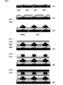
- FIG. 2 is a schematic cross-sectional view and a plan view showing an example of a display device including a pixel dividing layer having a stepped shape.
- FIG. 1 is a schematic cross-sectional view and a plan view showing an example of a display device including a pixel dividing layer and a spacer layer.
- FIG. 2 is a schematic cross-sectional view and a plan view showing an example of a display device including a pixel dividing layer and a pixel size control layer having a stepped shape.
- FIG. 3 is a plan view showing an example of the shape of a pixel section, the shape of a color filter layer section, and the shape of an opening section of a black matrix layer section.
- FIG. 1 is a schematic cross-sectional view and a plan view showing an example of a display device including a pixel dividing layer and a spacer layer.
- FIG. 2 is a schematic cross-sectional view and a plan view showing an example of a display device including a pixel
- FIG. 2 is a schematic cross-sectional view and a plan view showing an example of a display device having a configuration in which a black matrix layer portion overlaps a color filter layer portion.
- FIG. 2 is a schematic cross-sectional view showing an example of a display device including a pixel dividing layer and a polarizing film having a stepped shape.
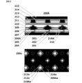
- FIG. 2 is a plan view showing an example of a display device having a configuration including a first color pixel section, a second color pixel section, and a third color pixel section.
- FIG. 3 is a schematic cross-sectional view showing an example of a cross-section of a cured pattern having a stepped shape.
- FIG. 2 is a schematic cross-sectional view showing an example of a manufacturing process of steps 1 to 6 in a display device including a pixel dividing layer having a stepped shape.
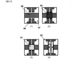
- FIG. 3 is a plan view showing the manufacturing process of steps 1 to 4 of a substrate of an organic EL display used for evaluation of light emitting characteristics.
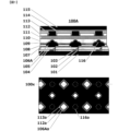
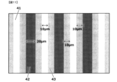
- FIG. 3 is a plan view showing an example of the arrangement and dimensions of a light-transmitting part, a light-shielding part, and a semi-light-transmitting part in a halftone photomask used for evaluating halftone characteristics.
- FIG. 2 is a plan view showing an example of the arrangement and dimensions of a thick film part, an opening part, and a thin film part of an organic EL display used for evaluating light emission characteristics.
- display devices that are the first and second aspects of the present invention will be described.
- the display device of the present invention refers to the display device that is the first aspect and the second aspect of the present invention, and the cured product obtained by curing the photosensitive composition that is the third aspect of the present invention, which will be described later.
- This is a description of a display device including the following.
- a display device of a specific aspect it will be described as a display device of a first aspect.
- a plane in plan view refers to a plane horizontal to a substrate, which will be described later.
- planar view refers to the xy-axis viewed from the z-axis direction, where the plane horizontal to the substrate is the xy-axis plane, and the direction orthogonal to the xy-axis plane is the z-axis direction.
- a plan view of the light extraction side of the display device Note that when focusing on a specific member in a plan view, it is assumed that another member overlapping the specific member is seen through. If the substrate is not flat, a plane horizontal to an arbitrary pixel portion, which will be described later, is defined as an xy plane.
- overlapping means directly or indirectly overlapping in the z-axis direction.
- the average value of pattern dimensions can be calculated as the average value obtained by measuring pattern dimensions at 30 points using an optical microscope or a scanning electron microscope (hereinafter referred to as "SEM").
- the maximum and minimum values of the pattern dimensions can be similarly calculated as the maximum and minimum values obtained by measuring the pattern dimensions at 30 points using an optical microscope or SEM.
- the main chain of the resin refers to the chain with the longest chain length among the chains constituting the resin including structural units.
- the side chain of a resin refers to a chain that is branched from or bonded to the main chain and has a chain length shorter than the main chain among the chains constituting the resin containing structural units.
- the terminus of the resin refers to a structure that seals the main chain, and is, for example, a structure derived from an end-capping agent.
- a hydrocarbon group or alkylene group containing a "** bond” or "** group” refers to a hydrocarbon group or alkylene group to which a "** bond" or "** group” is bonded, or a "* Refers to at least two hydrocarbon groups or at least two alkylene groups connected by a *bond or a ** group.
- a display device is a display device having an organic layer including a substrate, a first electrode, a second electrode, a pixel dividing layer, and a light emitting layer,
- the pixel dividing layer contains a (D-DL) colorant, and the optical density at the wavelength of visible light per 1 ⁇ m of film thickness of the pixel dividing layer is 0.5 to 3.0, In plan view, it has a plurality of pixel parts, Measured by time-of-flight secondary ion mass spectrometry at a depth of 3 nm from the surface of the first electrode on the side in contact with the organic layer including the light-emitting layer in the pixel portion.
- the detection intensity of sulfur ions (S ⁇ ) is defined as (S Dep/Anode ) counts
- the detection intensity of chlorine ion (Cl ⁇ ) is defined as (Cl Dep/Anode ) counts
- the display device satisfies the relationship expressed by general formula (SA-1) and/or the relationship expressed by general formula (XA-1). 2 ⁇ (S Dep/Anode ) ⁇ 200 (SA-1) 2 ⁇ (X Dep/Anode ) ⁇ 200 (XA-1).
- the display device of the present invention can have both excellent light emission characteristics that can be driven at a low voltage and high reliability of the light emitting element.
- the higher the detection intensity of sulfur ions, chlorine ions, and bromine ions on the surface of the first electrode in contact with the organic layer including the light emitting layer the more likely the surface is modified by these elements on the surface of the first electrode.
- the polarization structure and charge balance on the first electrode in an organic EL display can be controlled. It is estimated that this suppresses ion migration and electromigration caused by metal impurities and ionic impurities that adversely affect light-emitting characteristics, thereby achieving high reliability of the light-emitting element. Furthermore, it is estimated that the light-emitting element has a highly reliable effect by suppressing migration and aggregation of the metal in the first electrode. Furthermore, the effect of high reliability of the light emitting element is achieved.
- a display device is a display device having an organic layer including a substrate, a first electrode, a second electrode, a pixel dividing layer, and a light emitting layer,
- the pixel dividing layer contains a (D-DL) colorant, and the optical density at the wavelength of visible light per 1 ⁇ m of film thickness of the pixel dividing layer is 0.5 to 3.0
- the pixel dividing layer contains one or more types selected from the group consisting of the following (I1a-DL) compounds, (I1b-DL) compounds, (I2a-DL) compounds, and (I2b-DL) compounds, (I1a-DL) compound and (I2a-DL) compound have the following (I-Ia) structure,
- the (I1b-DL) compound and the (I2b-DL) compound have the following (I-Ib) structure, which is a display device.
- (I1a-DL) Compound from a thiol structure-containing compound, a sulfide structure-containing compound, a disulfide structure-containing compound, a sulfoxide structure-containing compound, a sulfone structure-containing compound, a sultone structure-containing compound, a thiophene structure-containing compound, and a sulfonic acid structure-containing compound
- One or more types of compounds selected from the group consisting of (I1b-DL) Compound One or more types selected from the group consisting of sulfide ion structure, hydrogen sulfide ion structure, sulfate ion structure, and hydrogen sulfate ion structure as anion species has, and A compound (I2a-DL) having an ammonium ion structure, a primary ammonium ion structure, a secondary ammonium ion structure, a tertiary ammonium ion structure, or a quaternary ammonium
- the content of sulfur element in the pixel dividing layer is 0.01 to 500 ppm by mass (1b-DL)
- the total content of sulfide ions, hydrogen sulfide ions, sulfate ions, and hydrogen sulfate ions in the pixel division layer is 0.01 to 1,000 ppm by mass (2a-DL)
- the total content of chlorine element and bromine element in the pixel division layer is 0.01 to 500 ppm by mass (2b-DL)
- the total content of chloride ions and bromide ions in the pixel dividing layer is 0.01 to 1,000 ppm by mass.
- the display device of the present invention can have both excellent light-emitting characteristics that can be driven at a low voltage and high reliability of the light-emitting element.
- the light emitting element has a highly reliable effect by suppressing migration and aggregation of the metal in the first electrode.
- the display device of the present invention has a substrate.
- the substrate preferably contains silicon dioxide or dialuminum trioxide, and more preferably a glass substrate, a quartz substrate, a crystal substrate, or a sapphire substrate.
- the substrate is preferably a flexible substrate from the viewpoints of improved flexibility, improved bendability, and improved shape freedom of the display device (curved shape, folded shape, etc.).
- the flexible substrate is preferably a substrate containing carbon as a main component from the viewpoint of improving the adhesion between the cured film of the present invention and the substrate and improving the bendability.
- the main component element in the flexible substrate refers to the element that is contained in the largest amount among the constituent elements of the flexible substrate.
- the flexible substrate is preferably a polyimide substrate, a polyethylene terephthalate substrate, a cycloolefin polymer substrate, a polycarbonate substrate, or a cellulose triacetate substrate, and from the viewpoint of improving bendability, a polyimide substrate is more preferable.
- the display device of the present invention preferably has a structure in which a pixel division layer, which will be described later, is laminated on a flexible substrate.
- the display device of the present invention is preferably a flexible display device, and preferably has a curved display portion, a display portion including an outwardly folded surface, or a display portion including an inwardly folded surface.
- the flexible display device is preferably a flexible organic EL display, a flexible quantum dot display, or a flexible micro LED display, and more preferably a flexible organic EL display.
- the display device of the present invention has a first electrode and a second electrode.
- a transparent electrode and a non-transparent electrode as the first electrode and the second electrode, it is possible to extract light emitted from an organic layer including a light emitting layer to be described later to one side.
- Transparent electrodes and non-transparent electrodes are required to have excellent electrical properties. When a transparent electrode or a non-transparent electrode is used as an anode, it is required to have multiple properties such as being able to efficiently inject holes, while when being used as a cathode, it is required to be able to inject electrons efficiently.
- a display device with a bottom emission type configuration has a transparent electrode as the first electrode and a non-transparent electrode as the second electrode.
- a display device having a top emission type configuration has a non-transparent electrode as the first electrode and a transparent electrode as the second electrode.
- the display device having a bottom emission type structure is preferably an organic EL display having a bottom emission type structure.
- the display device having a top emission type configuration is preferably an organic EL display having a top emission type configuration.
- a transparent electrode refers to an electrode having a transmittance of 30% or more at a wavelength of 550 nm.
- a non-transparent electrode refers to an electrode whose transmittance at a wavelength of 550 nm is less than 30%.
- the transmittance is measured using the transmittance at a wavelength of 550 nm when the electrode has a multilayer structure, and the electrode is classified as a transparent electrode or a non-transparent electrode.
- the first electrode, which is a non-transparent electrode has a multilayer structure.
- the first electrode, which is a non-transparent electrode may have a multilayer structure, and the first electrode may have a base layer on the substrate side that improves adhesion and corrosion resistance, and a reflection adjustment layer that adjusts reflectance.
- the electrode has a single-layer structure, transparent or non-transparent in the transparent conductive oxide film layer, non-transparent conductive layer, non-transparent conductive metal layer, transparent conductive layer, and transparent conductive metal layer described below means: Similarly to the above, it means that the transmittance at a wavelength of 550 nm is 30% or more or less than 30%. On the other hand, when the electrode has a multilayer structure, it is said to be transparent if the overall transmittance at a wavelength of 550 nm is 30% or more, and it is called non-transparent if the transmittance of even one of the layers constituting the multilayer structure is less than 30%.
- the electrode comprising the multilayer structure is a non-transparent electrode.
- each layer constituting the multilayer structure preferably has a transmittance of 70% or more at a wavelength of 550 nm.
- the display device of the present invention has a plurality of first electrode parts in a plan view.
- a plan view of the first electrode described above corresponds to the first electrode portion.
- the display device of the present invention has a second electrode part in a plan view.
- a plan view of the second electrode described above corresponds to the second electrode portion.
- the display device of the present invention has a plurality of second electrode parts. The shape of the first electrode part when the display device of the present invention has a plurality of first electrode parts, and the shape of the second electrode part when the display device of the present invention has a plurality of second electrode parts are closed.
- a polygon a shape in which at least some of the sides and/or vertices of a closed polygon are replaced with circular arcs, or a closed shape formed of circular arcs are preferable.
- Examples and preferred descriptions of closed polygons, shapes in which at least some of the sides and/or vertices of a closed polygon are replaced with circular arcs, and closed shapes formed of circular arcs are as described below. .
- the display device of the present invention preferably has a transparent conductive oxide film layer on the outermost layer on the light emitting layer side of the first electrode, and the display device preferably has a transparent conductive oxide film layer containing In, Sn, Zn, Al, or Ga as a main component. It is more preferable to have a transparent conductive oxide film layer, and it is even more preferable to have a transparent conductive oxide film layer containing indium as a main component element.
- the main component element in the transparent conductive oxide film layer refers to an element other than oxygen that is contained in the largest amount among the constituent elements of the transparent conductive oxide film layer.
- the transparent conductive oxide film layer containing In, Sn, Zn, Al, or Ga as a main component is preferably ITO or IZO, more preferably ITO, from the viewpoint of driving the light emitting characteristics at a low voltage and improving the light emission brightness.
- the transparent conductive oxide film layer is preferably an amorphous transparent conductive oxide film layer from the viewpoint of driving the light emitting characteristics at a low voltage and improving the reliability of the light emitting device.
- a neutral oxide film layer is more preferable.
- the transparent conductive oxide film layer is preferably a polycrystalline transparent conductive oxide film layer, and more preferably a polycrystalline transparent conductive oxide film layer containing indium as a main component element.
- these transparent conductive oxide film layers are provided on the outermost layer of the first electrode on the light emitting layer side. It is preferable to have.
- the first electrode has a single layer structure or a multilayer structure. When the first electrode has a single layer structure, the first electrode is preferably a transparent electrode.
- the first electrode When the first electrode has a multilayer structure, the first electrode is a transparent electrode or a non-transparent electrode.
- the first electrode When the first electrode is used as an anode, the first electrode is preferably ITO or IZO, more preferably ITO, from the viewpoint of driving the light emitting characteristics at a low voltage and improving the light emission brightness.
- the first electrode When the first electrode is a transparent electrode, it is preferable to adjust the film thickness of the first electrode to adjust the transmittance at a wavelength of 550 nm.
- the first electrode When the first electrode is a non-transparent electrode with a single layer structure, the first electrode is a non-transparent conductive layer. When the first electrode is a non-transparent electrode with a multilayer structure, the first electrode has a non-transparent conductive layer. It is preferable that at least one layer other than the outermost layer on the light-emitting layer side of the first electrode is a non-transparent conductive layer. Regardless of whether the first electrode is a non-transparent electrode and has a single-layer structure or a multi-layer structure, the non-transparent conductive layer is preferably a non-transparent conductive metal layer containing a metal element.
- the non-transparent conductive metal layer is made of Ag, Cu, Au, etc., from the viewpoints of low voltage driving of the light emitting characteristics, improvement of luminescence brightness, improvement of reliability of the light emitting element, and improvement of corrosion resistance. , Ti, Al, Ni, Mo, or Cr as the main component, more preferably Ag, Cu, Au, Ti, or Al as the main component, and silver or copper as the main component. It is more preferable to include it as an element.
- the non-transparent conductive metal layer further contains In, Sn, Zn, Al, Ga, Pd, Cu, Bi, Nd, Ni, Mn, Na, K, Mg, Ca, C, as elements different from the main component elements.
- the main component element in the non-transparent conductive metal layer refers to the element that is contained in the largest amount among the constituent elements of the non-transparent conductive metal layer.
- the first electrode is a non-transparent electrode, it is preferable to adjust the thickness of the first electrode to adjust the transmittance at a wavelength of 550 nm.
- the display device of the present invention preferably has a transparent conductive metal layer on the outermost layer on the light emitting layer side of the second electrode, and has a transparent conductive metal layer containing Li, Mg, Ag, Cu, Au, Ti, or Al as a main component. It is more preferable to have a transparent conductive metal layer containing magnesium or silver as a main component element.
- the main component element in the transparent conductive metal layer refers to the element that is contained in the largest amount among the constituent elements of the transparent conductive metal layer.
- the transparent conductive metal layer containing Li, Mg, Ag, Cu, Au, Ti, or Al as a main component is preferably LiAg or MgAg, and more preferably MgAg, from the viewpoint of improving luminance.
- the second electrode whether the second electrode has a multilayer structure and is a transparent electrode or a non-transparent electrode, these transparent conductive metal layers are provided on the outermost layer of the second electrode on the light emitting layer side. It is preferable to have.
- the transparent conductive metal layer or the non-transparent conductive metal layer is made of Li, Mg, Ag, Cu, Au, Ti, or Al, from the viewpoint of improving luminance and reliability of the light emitting element. It is more preferable to have a transparent conductive metal layer containing as a main component element. From the viewpoint of improving luminance, the transparent conductive metal layer is preferably LiAg or MgAg, and more preferably MgAg.
- the second electrode is a transparent electrode or a non-transparent electrode, it is preferable to adjust the thickness of the second electrode to adjust the transmittance at a wavelength of 550 nm.
- the first electrode is a non-transparent electrode with a multilayer structure, and the first electrode has a non-transparent conductive metal layer, from the viewpoint of driving the light emission characteristics at a low voltage and improving the light emission brightness. It is preferable that at least one layer of the first electrode other than the outermost layer on the light emitting layer side has a non-transparent conductive metal layer containing silver or copper as a main component element.
- the first electrode is formed of a transparent conductive oxide film layer from the viewpoint of driving the light emitting characteristics at a low voltage and improving the reliability of the light emitting element. and a non-transparent conductive metal layer, and preferably has a transparent conductive oxide film layer containing indium as a main component on the outermost layer on the light-emitting layer side of the first electrode.
- the first electrode is a non-transparent electrode with a multilayer structure, and the first electrode is a transparent conductive electrode, from the viewpoint of lower voltage driving of the light emission characteristics, improvement of the luminance, and improvement of the reliability of the light emitting element.
- the first electrode has an amorphous transparent conductive oxide film layer containing indium as a main component on the outermost layer on the light emitting layer side of the first electrode. It is preferable that at least one layer of the electrode other than the outermost layer on the light emitting layer side has a non-transparent conductive metal layer containing silver or copper as a main component, and has a top emission type structure.
- the silver or copper contained in the non-transparent conductive metal layer has excellent low resistance characteristics, the effects of lower voltage driving of the light emitting characteristics and improvement of the light emission brightness are remarkable. Further, it is estimated that the adjustment of the work function difference by the indium contained in the transparent conductive oxide film layer will significantly improve the effect of lower voltage driving of the light emitting characteristics and improvement of the reliability of the light emitting element.
- the amorphous transparent conductive oxide film layer suppresses the occurrence of defects, and the top-emission structure reduces stray light and scattered light inside the device, making it possible to increase the driving voltage to ensure luminance. It is estimated that the effect of improving the reliability of the light-emitting element will be significant because it can be suppressed.
- the outermost amorphous conductive oxide film layer is easily surface modified by sulfur elements, chlorine elements, and bromine elements, and the light emitting characteristics can be driven at lower voltages by adjusting the work function difference, and the light emitting element can be It is estimated that the effect of improving reliability will be significant.
- the light extraction efficiency is improved due to the high reflectance characteristics of these metals, so it is possible to lower the voltage driving of the light emitting characteristics and improve the light extraction efficiency. It is estimated that the effect of improving luminance will be significant. Similarly, since conductivity is improved due to the low resistivity characteristic of these metals, it is estimated that the effects of lower voltage driving of the light emitting characteristics and improvement of light emission brightness will be significant.
- An amorphous transparent conductive oxide film layer and a non-transparent conductive metal layer containing silver or copper as the main element enable lower voltage driving of light emitting characteristics, improved reliability of light emitting elements, improved luminance, and light extraction. Since the effect of improving efficiency is significant, it is particularly suitable for display devices having a top emission type configuration.
- the total content ratio of the silver element and the copper element in the non-transparent conductive metal layer containing silver or copper as a main component element in the first electrode is determined by the low voltage drive of the light emitting characteristics due to high reflectance and low resistivity. From the viewpoint of improving the luminance and emission brightness, the content is preferably 95% by mass or more, more preferably 96% by mass or more, and even more preferably 97% by mass or more. On the other hand, the total content ratio of the silver element and the copper element is preferably 99.5% by mass or less, and 99% by mass or less, from the viewpoint of low-voltage driving of the luminescent characteristics and improvement of luminescence brightness due to high reflectance and low resistivity. is more preferable, and even more preferably 98.5% by mass or less.
- the non-transparent conductive metal layer containing silver as a main component element in the first electrode preferably further contains copper and/or palladium as an element different from the main component element, and more preferably contains copper and palladium. preferable. Further, the non-transparent conductive metal layer containing copper as a main component element in the first electrode preferably further contains silver and/or palladium as an element different from the main component element, and preferably contains silver and palladium. is more preferable.
- the conductivity of the first electrode is improved, so it is estimated that the effects of lower voltage driving of the light emitting characteristics and improvement of the light emission brightness become more significant. Furthermore, since the heat resistance and oxidation resistance of the first electrode are significantly improved, it is estimated that the effect of improving the reliability of the light emitting element will be significant.
- the total content ratio of the copper element and the palladium element in the non-transparent conductive metal layer containing silver as the main component element in the first electrode is determined by the following: From the viewpoint of improving reliability, the content is preferably 0.1% by mass or more, more preferably 0.5% by mass or more, and even more preferably 1.0% by mass or more. On the other hand, the total content ratio of the copper element and the palladium element is preferably 5% by mass or less, more preferably 4% by mass or less, from the viewpoint of driving the light emission characteristics at a low voltage, improving the luminance brightness, and improving the reliability of the light emitting element. It is preferably 3% by mass or less, and more preferably 3% by mass or less.
- the total content ratio of silver element and palladium element in the non-transparent conductive metal layer containing copper as a main component element in the first electrode is determined by the total content ratio of silver element and palladium element, which contributes to low voltage driving of the light emission characteristics, improvement of light emission brightness, and light emission.
- the content is preferably 0.1% by mass or more, more preferably 0.5% by mass or more, and even more preferably 1.0% by mass or more.
- the total content ratio of the silver element and the palladium element is preferably 5% by mass or less, more preferably 4% by mass or less, from the viewpoints of driving the light emitting characteristics at a lower voltage, improving the luminance brightness, and improving the reliability of the light emitting element. It is preferably 3% by mass or less, and more preferably 3% by mass or less.
- the first electrode is a non-transparent electrode with a multilayer structure
- the first electrode has a transparent conductive oxide film layer and a non-transparent conductive metal layer
- the first electrode has a transparent conductive oxide film layer and a non-transparent conductive metal layer
- the outermost layer has an amorphous transparent conductive oxide film layer containing indium as a main component element, and at least one layer other than the outermost layer on the light emitting layer side of the first electrode contains silver or copper as a main component.
- the non-transparent conductive metal layer containing silver or copper as a main component element in the first electrode further contains In, Sn, Zn, Al, Ga, It is preferable to include one or more selected from the group consisting of Bi, Nd, Ni, Mn, Na, K, Mg, Ca, C, and Si, including In, Sn, Al, Na, K, Mg, Ca, It is more preferable to include one or more types selected from the group consisting of and Si, and it is even more preferable to include one or more types selected from the group consisting of Na, K, Mg, and Ca.
- the non-transparent conductive metal layer containing silver as a main element in the first electrode contains copper and/or palladium, and preferably further contains these elements.
- the non-transparent conductive metal layer containing copper as a main component element in the first electrode contains silver and/or palladium, and preferably further contains these elements.
- the total content ratio of each element, C and Si is preferably 0.1% by mass or more, more preferably 0.5% by mass or more, from the viewpoint of driving the light emission characteristics at a low voltage and improving the luminance brightness.
- the total content ratio of each element of In, Sn, Zn, Al, Ga, Bi, Nd, Ni, Mn, Na, K, Mg, Ca, C, and Si is the From the viewpoint of improving luminance, the content is preferably 3% by mass or less, more preferably 2% by mass or less.
- the display device of the present invention has a pixel dividing layer.
- the pixel division layer is a layer that divides adjacent pixel parts and defines the area of each pixel part.
- the pixel dividing layer is a layer that divides a region on the first electrode. Note that when the display device of the present invention has a pixel size control layer described later, the pixel size control layer also divides adjacent pixel parts, and the pixel size control layer is a layer that defines the area and size of each pixel part. Become.
- the pixel dividing layer is preferably a cured film obtained by curing a photosensitive composition, more preferably a cured film obtained by curing a photosensitive composition containing a colorant, and even more preferably a cured film obtained by curing a photosensitive composition containing a black agent. It is preferable that the pixel division layer is formed so as to partially overlap with the above-described first electrode. With such a configuration, the first electrode and the second electrode in any pixel can be insulated, and it is possible to suppress the pixel from turning off due to a short circuit between the first electrode and the second electrode. Further, the first electrode in any pixel can be insulated from the first electrode in an adjacent pixel, and it is possible to suppress the pixel from turning off due to a short circuit between the first electrodes.
- the pixel dividing layer is preferably black at the wavelength of visible light due to the coloring of components such as resin in the photosensitive composition, and in addition to the coloring of components such as resin, thermal color formers and/or oxidative color formers, etc. It is more preferable that the color is black.
- the pixel dividing layer is more preferably black due to coloring with a plurality of colorants, and even more preferably black due to coloration with a thermal color former and/or an oxidative color former in addition to the coloration with a plurality of colorants. preferable. It is particularly preferred that the pixel dividing layer is black with a black agent. Note that colored means red, orange, yellow, green, blue, or purple.
- the display device of the present invention has a pixel division layer portion having a plurality of openings in plan view.
- a plan view of the above-mentioned pixel division layer corresponds to the pixel division layer portion.
- the shape of the pixel portion which will be described later, is preferably similar to or similar to the shape of the opening of the pixel dividing layer, and is preferably the same as the shape of the opening of the pixel dividing layer. More preferred.
- the shape of the pixel section described below is preferably similar to or similar to the shape of the opening of the pixel size control layer section. It is more preferable that the shape of the opening is the same as that of the opening of the pixel size control layer.
- the shape of the pixel portion is preferably a closed polygon, a shape in which at least some of the sides and/or vertices of a closed polygon are replaced with circular arcs, or a closed shape formed by circular arcs.
- closed polygons include triangles, equilateral triangles, isosceles triangles, right triangles, quadrilaterals, squares, rhombuses, rectangles, trapezoids, right trapezoids, and parallelograms.
- Examples of shapes in which at least some of the sides and/or vertices of a closed polygon are replaced with circular arcs include triangles, equilateral triangles, isosceles triangles, right triangles, quadrilaterals, squares, rhombuses, rectangles, trapezoids, and right trapezoids. , or a shape in which at least some of the sides and/or vertices of a parallelogram are replaced with circular arcs.
- Examples of the closed shape formed by a circular arc include a circle, a perfect circle, and an ellipse.
- the shape of the pixel portion is preferably a quadrilateral, a square, a rhombus, or a rectangle; a shape in which at least some of the sides and/or vertices of a quadrilateral, square, rhombus, or rectangle are replaced with arcs, or a circle or a perfect circle.
- the shape of the pixel part is a closed polygon, or at least some of the sides and/or vertices of the closed polygon are replaced with circular arcs from the viewpoints of suppressing reflection of external light, driving the light emitting characteristics at a low voltage, and improving the light emission brightness.
- a rounded shape is preferred.
- the light emitted from the light emitting element becomes asymmetrical as surface light emission, and is strengthened by reflection and interference between the first electrode and the second electrode, so the light emission It is estimated that the effects of lower voltage driving characteristics and improved luminance will be noticeable.
- the scattering of incident external light on the surface of the pixel dividing layer part becomes asymmetrical, and the reflection between the first electrode and the second electrode becomes asymmetric. It is estimated that the effect of suppressing reflection of external light becomes significant because it is weakened by interference.
- the shape of the opening in the overcoat layer is preferably a closed polygon, a closed polygon with at least some of its sides and/or vertices replaced with circular arcs, or a closed polygon formed by circular arcs. . Examples and preferred descriptions of closed polygons, shapes in which at least some of the sides and/or vertices of a closed polygon are replaced with circular arcs, and closed shapes formed of circular arcs are as described above.
- the shape of the color filter layer section which will be described later and overlaps with the pixel section, is preferably similar to or similar to the shape of the pixel section.
- the shape of the opening in the black matrix layer section which will be described later, overlaps with the pixel section, and preferably has a similar shape or a similar shape to the shape of the pixel section.
- the shape of the color filter layer is preferably similar to or similar to the shape of the opening of the black matrix layer. It is more preferable that the shape of the pixel part, the shape of the color filter layer part, and the shape of the opening part of the black matrix layer part are all similar or similar shapes.
- any one of the shapes of the pixel portion, the shape of the color filter layer portion, and the shape of the opening portion of the black matrix layer portion may not be similar or similar shapes.
- the shape of the pixel section, the shape of the color filter layer section, and the shape of the opening section of the black matrix layer section do not have to be similar or similar to each other.
- FIG. 4 is a plan view showing an example of the shape of the pixel section, the shape of the color filter layer section, and the shape of the opening section of the black matrix layer section.
- the shape of the pixel portion, the shape of the opening in the pixel dividing layer, the shape of the opening in the pixel size control layer (described later), the shape of the spacer layer (described later), the shape of the color filter layer (described later), the black matrix layer (described later) The pattern dimensions in the major axis direction and the pattern dimensions in the minor axis direction in the shape of the opening of the overcoat layer section, the shape of the overcoat layer section described below, and the shape of the opening of the overcoat layer section described below will be described below.
- the pattern dimension in the major axis direction refers to the length of the longest straight line among the straight lines that symmetrically divide the closed polygon into two.
- the pattern dimension in the short axis direction refers to the length of the longest straight line among the straight lines in the direction perpendicular to the long axis direction.
- the pattern dimension in the long axis direction means that at least some of the sides and/or vertices of the closed polygon are replaced with circular arcs.
- the pattern dimension in the short axis direction refers to the length of the longest straight line among the straight lines in the direction perpendicular to the long axis direction.
- the pattern dimension in the major axis direction refers to the length of the longest straight line among the straight lines that symmetrically divide the closed shape formed by a circular arc into two.
- the pattern dimension in the short axis direction refers to the length of the longest straight line among the straight lines in the direction perpendicular to the long axis direction.
- the pattern dimension in the major axis direction refers to the diameter of the longest circle.
- the pattern dimension in the short axis direction refers to the diameter of a circle in the direction perpendicular to the long axis direction.
- the pattern dimensions of the openings in the pixel dividing layer section and the openings in the pixel size control layer section described below refer to the length from bottom to bottom of the openings.
- the average value of the pattern dimensions in the long axis direction of the openings in the pixel dividing layer section or the openings in the pixel size control layer section is used to suppress reflection of external light, lower voltage driving of light emitting characteristics, improve luminance, and improve reliability of light emitting elements.
- the thickness is preferably 5.0 ⁇ m or more, more preferably 6.0 ⁇ m or more, even more preferably 7.0 ⁇ m or more, even more preferably 8.0 ⁇ m or more, and particularly preferably 10.0 ⁇ m or more.
- the average value of the pattern dimensions in the long axis direction of the openings of the pixel dividing layer section or the openings of the pixel size control layer section described below is preferably 50.0 ⁇ m or less from the viewpoint of suppressing reflection of external light and improving luminance. , more preferably 40.0 ⁇ m or less, and even more preferably 35.0 ⁇ m or less.
- the average value of the pattern dimensions in the long axis direction of the openings in the pixel dividing layer section or the openings in the pixel size control layer section can be used to suppress reflection of external light, lower voltage driving of the light emitting characteristics, improve luminance, and improve the light emitting element.
- the thickness is preferably 30.0 ⁇ m or less, more preferably 25.0 ⁇ m or less, even more preferably 20.0 ⁇ m or less, even more preferably 17.0 ⁇ m or less, and particularly preferably 15.0 ⁇ m or less.
- the pattern dimension in the long axis direction of the pixel section refers to the length from bottom to bottom in the pixel section.
- the pattern dimension in the long axis direction of the pixel part is (CD) ⁇ m
- the pattern dimension in the long axis direction of the opening of the pixel division layer part or the opening of the pixel size control layer part corresponding to the pixel part is (DL).
- the dimensional difference ( ⁇ CD-DL) ⁇ m between (CD) ⁇ m and (DL) ⁇ m is preferably ⁇ 2.0 ⁇ m or more, more preferably ⁇ 1.5 ⁇ m or more, and still more preferably ⁇ 1.0 ⁇ m or more.
- the dimensional difference ( ⁇ CD-DL) ⁇ m between (CD) ⁇ m and (DL) ⁇ m is preferably 2.0 ⁇ m or less, more preferably 1.5 ⁇ m or less, even more preferably 1.0 ⁇ m or less, and 0.5 ⁇ m or less. is even more preferable, and 0.2 ⁇ m or less is particularly preferable. It is most preferable that the pattern size in the long axis direction of the pixel portion is the same as the pattern size in the long axis direction of the opening of the pixel dividing layer portion or the opening of the pixel size control layer portion corresponding to the pixel portion.
- the display device of the present invention further includes a pixel size control layer.
- the pixel size control layer is a layer that is in contact with both the pixel division layer and the pixel section and adjusts the size of the area of each pixel section.
- the pixel size control layer is preferably a layer that adjusts the size of the area on the first electrode divided by the pixel division layer.
- the pixel size control layer is preferably a cured film obtained by curing a photosensitive composition. It is preferable that the pixel size control layer is formed so as to partially overlap with the above-described first electrode.
- the pattern dimensions of the openings serving as pixel portions can be controlled with high precision, so that the effect of improving the pattern dimension uniformity becomes remarkable.
- the pattern dimensions of the pixel section, the pattern dimensions of the color filter layer section, and the pattern dimensions of the opening section of the black matrix layer section can be controlled with high precision, suppressing the reflection of external light, lowering the voltage driving of the light emitting characteristics, and increasing the luminance. and the effect of improving the reliability of the light emitting element becomes remarkable.
- the display device of the present invention further includes a pixel size control layer portion having a plurality of openings in plan view.
- “covering” means that at least a portion thereof directly overlaps in the z-axis direction.
- a plan view of the above-mentioned pixel size control layer corresponds to the pixel size control layer section.
- FIG. 3 shows a schematic cross-sectional view and a plan view of an example of a display device including a pixel dividing layer and a pixel size control layer having a stepped shape.
- the display device of the present invention further includes a spacer layer.
- the spacer layer is a layer located above and/or below the pixel division layer. By having the spacer layer, even when the pixel dividing layer does not have a step shape, it is possible to provide a function corresponding to the thick film portion when the pixel dividing layer has a step shape.
- the spacer layer preferably includes a spacer layer above the pixel dividing layer and/or a lower spacer layer located below the pixel dividing layer.
- the spacer layer is preferably a cured film obtained by curing a photosensitive composition.
- the spacer layer is formed on a portion of the pixel division layer.
- the contact area between the pixel division layer and the vapor deposition mask when forming the organic layer including the light emitting layer can be reduced. Therefore, by suppressing damage to the pixel division layer, the effect of suppressing a decrease in panel yield and improving the reliability of light emitting elements becomes significant.
- the display device of the present invention further includes a spacer layer portion in a plan view.
- a plan view of the spacer layer described above corresponds to the spacer layer portion.
- the shape of the spacer layer is preferably a closed polygon or a shape in which at least some of the sides and/or vertices of the closed polygon are replaced with circular arcs.
- the pixel dividing layer contains a (DDL) colorant.
- incident external light can be blocked by the pixel division layer, so that the effect of suppressing reflection of external light becomes significant.
- the light-shielding properties of the pixel dividing layer at visible light wavelengths and wavelengths in the ultraviolet region, outgassing from the pixel dividing layer, etc. is suppressed, and deterioration of the light emitting element is suppressed, so the reliability of the light emitting element is improved. It becomes noticeable.
- the (D-DL) colorant in the pixel dividing layer is preferably a black agent and/or a colorant mixture of two or more colors.
- the (D-DL) colorant in the pixel dividing layer preferably contains a pigment and/or a dye, more preferably a pigment and a dye.
- the pixel dividing layer contains a (D-DL) colorant, and that the spacer layer satisfies at least one of the following conditions (1) to (3).
- the spacer layer more preferably satisfies at least one of the conditions (1) and (3) below, and even more preferably satisfies at least the condition (1) below.
- the spacer layer does not contain the (D-DL) colorant.
- the spacer layer contains the (D-DL) colorant, and the optical density at the wavelength of visible light per 1 ⁇ m of the spacer layer thickness is 0.
- the spacer layer contains a compound having a (C2x-DL) carboxylic acid ester structure containing an indene structure and/or a sulfonic acid aryl ester structure containing an indene structure.
- the pixel dividing layer and the spacer layer are formed by a two-layer film formation method using photosensitive compositions with different compositions, or the spacer layer is formed using a positive photosensitive composition. It is formed from a composition.
- the method of forming a two-layer film since the openings of the first layer come into contact with the alkaline developer again, the generation of residue at the openings of the pixel dividing layer section or the openings of the pixel size control layer section is suppressed. It is estimated that the effects of lower voltage driving of light emitting characteristics and improvement of light emission brightness will be significant.
- the first pixel dividing layer is not halftone exposed using a halftone photomask, but in the case of a negative type, photocuring is sufficiently progressed by fulltone exposure, and the solubility in alkaline developer is significantly reduced. are doing. Therefore, the surface of the first pixel division layer is a smooth film surface with little roughness, and it is estimated that the scattering of the incident external light is suppressed, so that the effect of suppressing reflection of external light becomes significant.
- the spacer layer is formed of a positive photosensitive composition, alkali dissolution in the openings is promoted by exposure to light, and the generation of development residue is suppressed. It is estimated that the effect will be significant.
- the (D-DL) colorant in the spacer layer is preferably a black agent and/or a colorant mixture of two or more colors.
- the (D-DL) colorant in the spacer layer preferably contains a pigment and/or a dye, more preferably a pigment and a dye.
- the (D-DL) colorant in the pixel dividing layer etc. preferably contains a black pigment and/or a mixture of two or more colored pigments from the viewpoint of suppressing reflection of external light and improving reliability of the light emitting device.
- the (D-DL) colorant in the pixel dividing layer etc. preferably contains a black dye and/or a mixture of two or more colored dyes from the viewpoint of suppressing external light reflection and improving the reliability of the light emitting device.
- the (D-DL) colorant in the pixel dividing layer etc. is preferably the (D) colorant described below.
- the pixel dividing layer etc. contain a black pigment.
- the incident external light can be blocked by the pixel division layer or the like, so that the effect of suppressing reflection of external light becomes significant.
- the light-shielding properties of the pixel dividing layer, etc. at visible light wavelengths and wavelengths in the ultraviolet region, outgassing from the pixel dividing layer, etc. is suppressed, and deterioration of the light emitting element is suppressed, resulting in the effect of improving the reliability of the light emitting element. becomes noticeable.
- the pixel dividing layer etc. contains an organic black pigment and/or a mixture of two or more colored pigments
- the organic black pigment includes one or more types selected from the group consisting of benzofuranone black pigments, perylene black pigments, and azo black pigments, It is preferable that the colored pigment mixture of two or more colors contains pigments of two or more colors selected from the group consisting of red, orange, yellow, green, blue, and violet.
- the organic black pigment more preferably contains a benzofuranone-based black pigment and/or a perylene-based black pigment, and even more preferably contains a benzofuranone-based black pigment.
- Colored pigment mixtures of two or more colors include anthraquinone pigments, diketopyrrolopyrrole pigments, perylene pigments, isoindoline pigments, isoindolinone pigments, imidazolone pigments, quinacridone pigments, pyranthrone pigments, and phthalocyanine pigments. , indanthrone pigments, and dioxazine pigments, and one or more pigments selected from the group consisting of perylene pigments, imidazolone pigments, and indanthrone pigments. It is more preferable to include the above pigments.
- the benzofuranone black pigment has at least two benzofuran-2(3H)-one structures that may share a benzene ring or at least two benzofuran-3(2H)-one structures that may share a benzene ring. is preferable, and it is more preferable to include a compound having a structure represented by either general formula (161) or general formula (162), a geometric isomer thereof, a salt thereof, or a salt of a geometric isomer thereof. .
- the pixel dividing layer etc. contains an organic black pigment and/or a mixture of two or more colored pigments
- the pixel dividing layer etc. contains a benzofuranone black pigment
- the benzofuranone black pigment is It is preferable to include a compound having a structure represented by either general formula (161) or general formula (162), a geometric isomer thereof, a salt thereof, or a salt of a geometric isomer thereof.
- the benzofuranone black pigment in the pixel dividing layer and the like is preferably a benzofuranone black pigment described below.
- benzofuranone black pigment in the pixel dividing layer etc. promotes a surface modification effect on the surface of the first electrode on the light emitting layer side corresponding to the opening of the pixel dividing layer or the opening of the pixel size control layer. Ru. Therefore, it is thought that adjustment of the work function difference promotes lower voltage driving of the light emitting characteristics. As a result, it is estimated that the effect of improving light emission brightness when driven at the same voltage becomes significant.
- benzofuranone black pigments have superior light-shielding properties per unit mass of the pigment compared to general organic pigments, and therefore have remarkable effects of suppressing reflection of external light and improving reliability of light-emitting devices.
- benzofuranone black pigments have excellent insulation properties and low dielectric properties compared to general organic pigments and inorganic pigments, and therefore have a remarkable effect of improving the reliability of light emitting devices.
- R 341 to R 344 each independently represent a hydrogen atom, a halogen atom, or an alkyl group having 1 to 10 carbon atoms.
- R 353 and R 354 each independently represent an alkyl group having 1 to 10 carbon atoms, a cycloalkyl group having 4 to 10 carbon atoms, an alkenyl group having 2 to 10 carbon atoms, a cycloalkenyl group having 4 to 10 carbon atoms, Or represents an alkynyl group having 2 to 10 carbon atoms.
- a plurality of R 345 to R 348 may be directly bonded to each other, or may form a ring through an oxygen atom bridge, a sulfur atom bridge, an NH bridge, or an NR 353 bridge.
- R 349 to R 352 each independently represent a hydrogen atom, an alkyl group having 1 to 10 carbon atoms, or an aryl group having 6 to 15 carbon atoms.
- a, b, c, and d each independently represent an integer of 0 to 4.
- the above-mentioned alkyl group, cycloalkyl group, alkenyl group, cycloalkenyl group, alkynyl group, and aryl group may have a heteroatom and may be unsubstituted or substituted.
- the perylene black pigment preferably has a perylene structure, more preferably contains a compound having a structure represented by any of the general formulas (164) to (166) or a salt thereof, and 3,4,9 , 10-perylenetetracarboxylic acid bisbenzimidazole structure, geometric isomers thereof, salts thereof, or salts of geometric isomers thereof.
- the perylene black pigment in the pixel dividing layer and the like is preferably a perylene black pigment described below.
- X 241 and X 242 each independently represent a direct bond or an alkylene group having 1 to 10 carbon atoms.
- Y 241 and Y 242 each independently represent a direct bond or an arylene group having 6 to 15 carbon atoms.
- R 361 and R 362 each independently represent a hydrogen atom, a hydroxy group, an alkyl group having 1 to 10 carbon atoms, an alkoxy group having 1 to 6 carbon atoms, or an acyl group having 2 to 6 carbon atoms.
- R 370 and R 371 each independently represent an alkyl group having 1 to 10 carbon atoms, a cycloalkyl group having 4 to 10 carbon atoms, an alkenyl group having 2 to 10 carbon atoms, a cycloalkenyl group having 4 to 10 carbon atoms, Or represents an alkynyl group having 2 to 10 carbon atoms.
- a plurality of R 367 to R 369 may be directly bonded to each other, or may form a ring through an oxygen atom bridge, a sulfur atom bridge, an NH bridge, or an NR 370 bridge.
- a and b each independently represent an integer of 0 to 5.
- c, d, e, and f each independently represent an integer of 0 to 4.
- g, h, and i each independently represent an integer of 0 to 8.
- X 241 and _ _ and b is 1.
- X 241 and X 242 are alkylene groups having 1 to 10 carbon atoms and Y 241 and Y 242 are a direct bond
- R 361 and R 362 are preferably hydroxy groups
- a and b are 1.
- X 241 and _ _ An alkoxy group having 1 to 6 carbon atoms or an acyl group having 2 to 6 carbon atoms is preferred, and a and b each independently represent an integer of 0 to 5.
- the above-mentioned alkylene group, arylene group, alkyl group, alkoxy group, and acyl group may have a heteroatom and may be unsubstituted or substituted.
- the azo black pigment preferably has an azo group, more preferably contains a compound having an azomethine structure and a carbazole structure, or a salt thereof, and contains a compound having a structure represented by general formula (168) or a salt thereof. It is even more preferable.
- the azo black pigment in the pixel dividing layer and the like is preferably an azo black pigment described below.
- X 251 represents an arylene group having 6 to 15 carbon atoms.
- Y 251 represents an arylene group having 6 to 15 carbon atoms.
- R 390 and R 391 each independently represent an alkyl group having 1 to 10 carbon atoms, a cycloalkyl group having 4 to 10 carbon atoms, an alkenyl group having 2 to 10 carbon atoms, a cycloalkenyl group having 4 to 10 carbon atoms, Or represents an alkynyl group having 2 to 10 carbon atoms.
- a plurality of R 381 to R 383 may be directly bonded to each other, or may form a ring through an oxygen atom bridge, a sulfur atom bridge, an NH bridge, or an NR 390 bridge.
- R 384 represents a halogen atom, an alkyl group having 1 to 10 carbon atoms, an alkoxy group having 1 to 6 carbon atoms, or a nitro group.
- R 385 represents a halogen atom, an alkyl group having 1 to 10 carbon atoms, an alkoxy group having 1 to 6 carbon atoms, an acylamino group having 2 to 10 carbon atoms, or a nitro group.
- R 386 to R 389 each independently represent a hydrogen atom or an alkyl group having 1 to 10 carbon atoms.
- a represents an integer from 0 to 4.
- b represents an integer from 0 to 2.
- c represents an integer from 0 to 4.
- d and e each independently represent an integer of 0 to 8.
- n represents an integer from 1 to 4.
- the above-mentioned arylene group, alkyl group, alkoxy group, and acylamino group may have a hetero atom, and may be unsubstit
- the primary particle size and average primary particle size of the pigment in the pixel dividing layer etc. are preferably 20 to 150 nm.
- the primary particle size and average primary particle size of the pigment in the pixel dividing layer etc. are preferably 20 nm or more, more preferably 30 nm or more, even more preferably 40 nm or more, and even more preferably 50 nm or more, from the viewpoint of improving the reliability of the light emitting device.
- the primary particle diameter of the pigment refers to the major axis diameter of the primary particles of the pigment.
- the primary particle diameter of the pigment in the pixel dividing layer, etc. can be measured using a transmission electron microscope (hereinafter referred to as " Image analysis method particle size distribution measurement is performed using a TEM (TEM) to observe areas located within a depth range of 0.2 to 0.8 ⁇ m from the surface of the pixel division layer at a magnification of 50,000 times. It can be measured using software (Mac-View; manufactured by MOUNTECH). Further, the average primary particle diameter of the pigment in the pixel dividing layer, etc. can be calculated as the average value obtained by imaging and analyzing the cross section of the measurement sample, and measuring 30 primary particles of the pigment in the pixel dividing layer, etc. Furthermore, the elements constituting the particles can be determined by observation using a transmission electron microscope-energy dispersive X-ray spectroscopy (hereinafter referred to as "TEM-EDX").
- TEM-EDX transmission electron microscope-energy dispersive X-ray spectroscopy
- the pixel dividing layer etc. contains a black dye and/or a mixture of two or more colored dyes, It is preferable that the black dye contains an azo black dye, and the mixture of two or more colored dyes contains two or more dyes selected from the group consisting of red, orange, yellow, green, blue, and violet.
- the black dye is preferably an azo black dye.
- the black dye is preferably Solvent Black 27 to 47, more preferably Solvent Black 27, 29, or 34 (all numerical values are C.I. numbers).
- black dyes examples include VALIFAST (registered trademark) Black 3804 (Solvent Black 34), VALIFAST (registered trademark) 3810 (Solvent Black 29), VALIFAST (registered trademark) 3820 (Solvent Black 27), VALIFAST (registered trademark) 3830 (Solvent Black 27), and NUBIAN (registered trademark) Black.
- the colored dye mixture of two or more colors preferably contains one or more dyes selected from the group consisting of squarylium dyes, xanthene dyes, triarylmethane dyes, and phthalocyanine dyes, and xanthene dyes and/or Or, it is more preferable that a triarylmethane dye is included, and it is even more preferable that a xanthene dye is included.
- squarylium dyes xanthene dyes, triarylmethane dyes, and phthalocyanine dyes, and xanthene dyes and/or
- a triarylmethane dye it is even more preferable that a xanthene dye is included.
- the pixel dividing layer and the like contain a (D-DL) colorant, and further include a compound having a structure derived from a thermal color former and/or a compound having a structure derived from an oxidized color former. is preferred. With such a configuration, the effect of suppressing reflection of external light and improving reliability of the light emitting element becomes remarkable.
- the compound having a structure derived from a thermal coloring agent is preferably a compound having a structure after the thermal coloring agent is structurally changed or decomposed by heating in an inert atmosphere, and more preferably a compound having a quinone structure and/or a quinoid structure. preferable. It is more preferable that the compound having a quinone structure and/or a quinoid structure includes the following (Q1) compound and/or (Q2) compound.
- the inert atmosphere is preferably a nitrogen, helium, neon, argon, krypton, or xenon atmosphere, a gas atmosphere containing less than 1 to 10,000 mass ppm (0.0001 to 1 mass %) of oxygen, or a vacuum.
- Q1 A compound having a quinone structure and/or a quinoid structure and an aromatic structure
- Q2 A compound having two or more quinone structures and/or two or more quinoid structures.
- the compound having a structure derived from an oxidized color former is preferably a compound having a structure after the oxidized color former is structurally changed or decomposed by heating in an oxygen-containing gas atmosphere, and a compound having a quinone structure and/or quinoid structure. is more preferable. It is more preferable that the compound having a quinone structure and/or a quinoid structure includes the above-mentioned (Q1) compound and/or (Q2) compound.
- the gas atmosphere containing oxygen is preferably air, an oxygen atmosphere, or a gas atmosphere containing 10,000 mass ppm (1 mass %) or more of oxygen.
- the pixel dividing layer etc. contain inorganic particles.
- the heat resistance of the pixel dividing layer etc. is significantly improved due to the robust structure of the inorganic particles in the pixel dividing layer etc., and outgassing from the pixel dividing layer etc. is suppressed.
- the inorganic particles in the pixel dividing layer and the like are preferably (H) inorganic particles described below.
- Inorganic particles in the pixel dividing layer etc. include Si, Al, Ti, V, Zn, Zr, Nb, Sn, Li, Cr, Mn, Fe, Co, Ni, Cu, Sr, Ag, Ba, La, Ce, It preferably contains Ta, W, or Re as a main element, and contains silicon, aluminum, titanium, vanadium, chromium, iron, cobalt, copper, zinc, zirconium, niobium, tin, or cerium as a main element. More preferably, it contains silicon as a main component element.
- the main component element in the inorganic particles refers to the element that is contained in the largest amount among the constituent elements of the inorganic particles.
- Inorganic particles in the pixel dividing layer, etc. include silica particles, alumina particles, titania particles, vanadium oxide particles, chromium oxide particles, iron oxide particles, cobalt oxide particles, copper oxide particles, zinc oxide particles, zirconium oxide particles, and niobium oxide particles. , tin oxide particles, or cerium oxide particles are preferable, and silica particles are more preferable.
- the pixel dividing layer etc. contain silica particles.
- deterioration of the light emitting element is suppressed similarly to the inorganic particles in the pixel dividing layer and the like, so that the effect of improving the reliability of the light emitting element becomes remarkable.
- the surface modification effect is promoted on the surface of the first electrode on the light emitting layer side, which corresponds to the opening of the pixel dividing layer or the opening of the pixel size control layer. Therefore, it is thought that adjustment of the work function difference promotes lower voltage driving of the light emitting characteristics. As a result, it is estimated that the effect of improving light emission brightness when driven at the same voltage becomes significant.
- the silica particles in the pixel dividing layer etc. reduce the reflection and scattering of incident external light on the surface of the pixel dividing layer etc., so the effect of suppressing reflection of external light becomes significant.
- the silica particles in the pixel dividing layer and the like are preferably (H1) silica particles described below.
- the primary particle size and average primary particle size of the silica particles in the pixel dividing layer etc. are preferably 5 to 50 nm.
- the primary particle size and average primary particle size of the silica particles in the pixel dividing layer etc. are preferably 5 nm or more, more preferably 7 nm or more, and even more preferably 10 nm or more, from the viewpoint of improving the reliability of the light emitting device.
- the primary particle diameter and average primary particle diameter of silica particles in the pixel dividing layer etc. are preferably 50 nm or less, more preferably 40 nm or less, and 30 nm or less from the viewpoint of suppressing external light reflection and improving the reliability of the light emitting element.
- the primary particle diameter of silica particles refers to the major axis diameter of primary particles of silica particles.
- silicon dioxide contained in the surface treatment agent or coating layer of organic pigments and inorganic pigments is not contained in silica particles regardless of their primary particle diameter or aspect ratio.
- the primary particle diameter and aspect ratio of the silica particles in the pixel dividing layer, etc. are measured using a TEM using a cross section of the pixel dividing layer, etc., which has been cut thinly and polished by ion milling processing to improve its smoothness. Images taken at a magnification of 50,000 times at locations located within a range of 0.2 to 0.8 ⁇ m in the depth direction from the surface of the pixel division layer, etc., were analyzed using image analysis particle size distribution measurement software (Mac-View; (manufactured by MOUNTECH). Further, the average primary particle diameter of the silica particles in the pixel dividing layer, etc.
- the elements constituting the particles can be determined, and the silica particles in the pixel dividing layer etc. can be identified.
- the pixel dividing layer etc. contains silica particles with a primary particle size or average primary particle size of 5 to 50 nm, and further includes silica particles with a primary particle size or average primary particle size of less than 5 nm, and/or a primary particle size or average primary particle size. It is also possible to contain silica particles having a primary particle diameter exceeding 50 nm.
- the silica particles in the pixel dividing layer etc. have a functional group on the surface.
- the functional groups that silica particles have on the surface include reactive residues of surface modifying groups including radically polymerizable groups, reactive residues of surface modifying groups including thermally reactive groups, silanol groups, alkoxysilyl groups, alkylsilyl groups, and dialkyl groups.
- a silyl group, a trialkylsilyl group, a phenylsilyl group, or a diphenylsilyl group is preferable, and from the viewpoint of suppressing reflection of external light, driving the light emitting characteristics at a low voltage, improving luminance, and improving the reliability of the light emitting device, radical polymerization is preferred.
- a reactive residue of a surface-modifying group containing a group or a reactive residue of a surface-modifying group containing a heat-reactive group is more preferable.
- the radically polymerizable group is preferably a styryl group, a cinnamoyl group, a maleimide group, a nadimide group, a (meth)acryloyl group, a vinyl group, or an allyl group.
- the heat-reactive group is preferably an alkoxymethyl group, a methylol group, an epoxy group, an oxetanyl group, or a blocked isocyanate group.
- the silica particles in the pixel dividing layer and the like preferably contain silica particles containing sodium element from the viewpoint of improving the reliability of the light emitting element.
- Examples of the existing form of sodium element include ions (Na + ) or salts with silanol groups (Si-ONa).
- the content of the sodium element in all the silica particles in the pixel dividing layer, etc. is preferably 1 mass ppm or more, more preferably 5 mass ppm or more, even more preferably 10 mass ppm or more, and particularly preferably 50 mass ppm or more.
- the amount is preferably 100 mass ppm or more, more preferably 300 mass ppm or more, and even more preferably 500 mass ppm or more.
- the content of sodium element in all the silica particles in the pixel dividing layer etc. is preferably 10,000 mass ppm or less, more preferably 7,000 mass ppm or less, even more preferably 5,000 mass ppm or less, and 3 ,000 mass ppm or less is even more preferred, and 1,000 mass ppm or less is particularly preferred.
- Silica particles containing elemental sodium are obtained by reacting sodium silicate, which is a strong alkali as a silicon source, with a mineral acid, which is a strong acid, under alkaline conditions.
- the sodium element contained in the silica particles can be detected at the center, which corresponds to the intersection of the long axis and the short axis, by imaging and analyzing the cross section of the primary particle of the silica particle using the above-mentioned TEM-EDX.
- the resins in the pixel dividing layer etc. will be described below.
- the pixel dividing layer etc. preferably contain the following (A1-DL) resin and/or (A3-DL) resin.
- (A1-DL) Resin Resin having a structural unit containing one or more types selected from the group consisting of imide structure, amide structure, oxazole structure, and siloxane structure
- (A3-DL) Resin Structural unit containing phenolic hydroxyl group resin with
- the effects of suppressing reflection of external light, driving the light emitting characteristics at a low voltage, improving the luminance of light emission, and improving the reliability of the light emitting element become remarkable.
- the (A1-DL) resin and (A3-DL) resin in the pixel division layer and the like absorb light of visible light wavelengths, so that the effect of suppressing reflection of external light becomes significant.
- the (A1-DL) resin and (A3-DL) resin in the pixel dividing layer etc. are applied to the surface of the light emitting layer side of the first electrode corresponding to the opening of the pixel dividing layer or the opening of the pixel size control layer. It is estimated that this promotes the surface modification effect on the surface.
- the (A3-DL) resin in the pixel division layer, etc. is a group consisting of a structure derived from the (A3) resin described below, a structure derived from the (A1) resin described below, and a structure derived from the resin (A2) described below. It is preferable that the resin has one or more types selected from the following.
- the pixel dividing layer and the like preferably contain the following (A2-DL) resin.
- the pixel dividing layer etc. contains (A1-DL) resin and/or (A3-DL) resin, and more preferably contains (A2-DL) resin. It is more preferable that the pixel division layer etc. contains (A1-DL) resin and (A2-DL) resin, and contains (A1-DL) resin, (A2-DL) resin, and (A3-DL) resin. It is particularly preferable to do so.
- (A2-DL) Resin A resin having a structural unit represented by general formula (24).
- R 67 to R 69 each independently represent a hydrogen atom or an alkyl group having 1 to 6 carbon atoms. a is 0 or 1. * 1 represents a bonding point in the resin.
- the structural unit represented by general formula (24) preferably contains a reactive residue of an ethylenically unsaturated double bond group.
- the reactive residue of an ethylenically unsaturated double bond group refers to a residue after radical polymerization of the ethylenically unsaturated double bond group by light and/or heat.
- the reactive residue of the ethylenically unsaturated double bond group is preferably a residue after radical polymerization of the ethylenically unsaturated double bond group in the resin (A2) described later, and the ethylene in the resin (A2) described later is preferable. More preferred are residues obtained by radical polymerization of the sexually unsaturated double bond group with the radically polymerizable compound (B) described later.
- the (A2-DL) resin in the pixel dividing layer and the like is a resin whose crosslinking density is improved by radically polymerizing a radically polymerizable group such as a (meth)acryloyl group.
- A2-DL It is estimated that the excellent heat resistance of the crosslinked structure of the resin suppresses outgassing from the pixel dividing layer and the like, so that the effect of improving the reliability of the light emitting device becomes significant.
- the (A2-DL) resin in the pixel dividing layer etc. is preferably a resin having a structure derived from the (A2) resin described below and/or a structure derived from the (A3) resin described below.
- the (A1-DL) resin in the pixel dividing layer etc. has the following general formulas (1), (2), (3), (4), (5), (6), (9) and (10). It is preferable to have one or more types selected from the group consisting of structural units represented by any of the above.
- the (A3-DL) resin in the pixel dividing layer etc. has general formulas (31), (32), (33), (34), (35), (36), (38), (39) and It is preferable to have one or more types selected from the group consisting of structural units represented by any of (40).
- These resins preferably have a phenolic hydroxyl group as an acidic group in at least one of the main chain of the resin, the side chain of the resin, and the end of the resin, and contain an aromatic ring skeleton in the structural unit of the resin. It is more preferable that the structural unit has a phenolic hydroxyl group as an acidic group and contains an aromatic ring skeleton. It is also preferable that some of the phenolic hydroxyl groups contained in the resin react with other resins or compounds to form a crosslinked structure.
- the (A2-DL) resin in the pixel dividing layer etc. has the following general formulas (1), (2), (3), (4), (5), (6), (9) and (10). It is preferable to have one or more types selected from the group consisting of structural units represented by any of the above.
- (A2-DL) resin in the pixel dividing layer etc. is a structural unit having a fused polycyclic structure; a structural unit having a fused polycyclic heterocyclic structure; a structure in which an aromatic ring skeleton and an alicyclic skeleton are directly connected. and a structural unit having a structure in which at least two aromatic ring skeletons are directly connected.
- the condensed polycyclic structure is preferably a naphthalene structure, a fluorene structure, or an indane structure.
- the fused polycyclic heterocyclic structure is preferably a xanthene structure, an indolinone structure, or an isoindolinone structure.
- the alicyclic skeleton preferably has a tricyclo[5.2.1.0 2,6 ]decane structure.
- the structure in which at least two aromatic ring skeletons are directly connected is preferably a biphenyl structure.
- a novolac structure has one or more types selected from the group consisting of a novolac structure, a cresol novolak structure, a triphenylalkane structure, a diphenyl-phenylalkylphenylalkane structure, and a diphenylalkane structure. It is preferable.
- the pixel dividing layer, etc. is made of a compound having a structure derived from a (C1-DL) photopolymerization initiator (hereinafter referred to as "(C1-DL) compound”) and/or a structure derived from a naphthoquinone diazide compound (C2-DL). (hereinafter referred to as "(C2-DL) compound”).
- (C1-DL) compound in the pixel dividing layer etc.
- the (C2-DL) compound in the pixel dividing layer etc. is a compound having a structure derived from a 1,2-naphthoquinonediazide-5-sulfonic acid ester compound and/or a 1,2-naphthoquinonediazide-4-sulfonic acid ester compound.
- Compounds having a structure derived from are preferred.
- the pixel dividing layer preferably contains a compound having a carboxylic acid ester structure containing an indene structure and/or a sulfonic acid aryl ester structure containing an indene structure.
- the effect of suppressing reflection of external light and improving reliability of the light emitting element becomes remarkable. It is presumed that this is because the (C1-DL) compound and (C2-DL) compound in the pixel dividing layer etc. absorb light of visible light wavelengths, so that the effect of suppressing external light reflection becomes significant.
- the (C1-DL) compound in the pixel dividing layer, etc. is contained in the pixel dividing layer, etc. after radical polymerization of a radically polymerizable compound having (meth)acryloyl group etc. to improve the crosslinking density of the film. It is a compound that has a residue.
- the (C1-DL) compound and (C2-DL) compound in the pixel dividing layer, etc. are incorporated as part of the crosslinked structure in the pixel dividing layer, etc., thereby improving the crosslinking density of the film. It is estimated that the effect of improving the reliability of the light-emitting element will be significant because outgassing from etc. is suppressed.
- the pixel dividing layer etc. contain the following (C1x-DL) compound and/or (C2x-DL) compound.
- (C1x-DL) Compound A structure having a fluorene structure, benzofluorene structure, dibenzofluorene structure, carbazole structure, benzocarbazole structure, indole structure, benzoindole structure, or diphenyl sulfide structure, with an imino group bonded to these structures.
- C2x-DL a structure in which a carbonyl group is bonded to these structures
- Compound a compound having a carboxylic acid ester structure containing an indene structure and/or a sulfonic acid aryl ester structure containing an indene structure.
- the (C1x-DL) compound in the pixel dividing layer etc. is preferably a compound having a fluorene structure, benzofluorene structure, dibenzofluorene structure, carbazole structure, or benzocarbazole structure, and has a structure in which an imino group is bonded to these structures. Compounds are more preferred.
- the (C2x-DL) compound in the pixel dividing layer etc. is a compound having a 1H-indene-3-carboxylic acid ester-7-sulfonic acid aryl ester structure and/or a 1H-indene-1-sulfonic acid aryl ester-3- Compounds having a carboxylic acid ester structure are preferred.
- the (C1x-DL) compound and (C2x-DL) in the pixel dividing layer etc. are present on the light emitting layer side surface of the first electrode corresponding to the opening of the pixel dividing layer or the opening of the pixel size control layer. It is presumed to promote surface modification effect. Therefore, it is thought that adjustment of the work function difference promotes lower voltage driving of the light emitting characteristics. As a result, it is estimated that the effect of improving light emission brightness when driven at the same voltage becomes significant.
- the (C1x-DL) compound in the pixel dividing layer, etc. is obtained by radically polymerizing a radically polymerizable compound having (meth)acryloyl group etc. to improve the crosslinking density of the film.
- the (C2x-DL) compound in the pixel dividing layer, etc. is a compound that has a residue contained in the pixel dividing layer, etc. after forming a crosslinked structure during thermosetting to improve the crosslinking density of the film. . Therefore, the (C1x-DL) compound and (C2x-DL) compound in the pixel dividing layer, etc. are incorporated as part of the crosslinked structure in the pixel dividing layer, etc., thereby improving the crosslinking density of the film. It is estimated that the effect of improving the reliability of the light-emitting element will be significant because outgassing from etc. is suppressed.
- the (C1-DL) compound and (C1x-DL) compound in the pixel dividing layer etc. are preferably compounds having a structure derived from the (C1) compound described below, and are derived from the (C1-1) compound described below. It is more preferable that the compound has the structure.
- the (C2-DL) compound and (C2x-DL) compound in the pixel dividing layer and the like are preferably compounds having a structure derived from the (C2) compound described below.
- the pixel dividing layer is made of the following (I1a-DL) compound, (I1b-DL) compound, (I2a-DL) compound, and (I2b-DL) compound.
- Contains one or more types selected from the group consisting of (I1a-DL) compound and (I2a-DL) compound have the following (I-Ia) structure
- the (I1b-DL) compound and the (I2b-DL) compound have the following (I-Ib) structure
- One or more of the following conditions (1a-DL) and (1b-DL) or one or more of the following conditions (2a-DL) and (2b-DL) are satisfied.
- (I1a-DL) Compound from a thiol structure-containing compound, a sulfide structure-containing compound, a disulfide structure-containing compound, a sulfoxide structure-containing compound, a sulfone structure-containing compound, a sultone structure-containing compound, a thiophene structure-containing compound, and a sulfonic acid structure-containing compound
- One or more types of compounds selected from the group consisting of (I1b-DL) Compound One or more types selected from the group consisting of sulfide ion structure, hydrogen sulfide ion structure, sulfate ion structure, and hydrogen sulfate ion structure as anion species has, and A compound (I2a-DL) having an ammonium ion structure, a primary ammonium ion structure, a secondary ammonium ion structure, a tertiary ammonium ion structure, or a quaternary ammonium
- the content of sulfur element in the pixel dividing layer is 0.01 to 500 ppm by mass (1b-DL)
- the total content of sulfide ions, hydrogen sulfide ions, sulfate ions, and hydrogen sulfate ions in the pixel division layer is 0.01 to 1,000 ppm by mass (2a-DL)
- the total content of chlorine element and bromine element in the pixel division layer is 0.01 to 500 ppm by mass (2b-DL)
- the total content of chloride ions and bromide ions in the pixel dividing layer is 0.01 to 1,000 ppm by mass.
- the pixel dividing layer etc. are selected from the group consisting of the following (I1a-DL) compounds, (I1b-DL) compounds, (I2a-DL) compounds, and (I2b-DL) compounds. It is preferable to contain one or more types.
- (I1a-DL) Compound from a thiol structure-containing compound, a sulfide structure-containing compound, a disulfide structure-containing compound, a sulfoxide structure-containing compound, a sulfone structure-containing compound, a sultone structure-containing compound, a thiophene structure-containing compound, and a sulfonic acid structure-containing compound
- One or more types of compounds selected from the group consisting of (I1b-DL) Compound One or more types selected from the group consisting of sulfide ion structure, hydrogen sulfide ion structure, sulfate ion structure, and hydrogen sulfate ion structure as anion species has, and A compound having an ammonium ion structure, a primary ammonium ion structure, a secondary ammonium ion structure, a tertiary ammonium ion structure, or a quaternary ammonium ion structure as a
- the compound containing the sulfur element and the compound containing the chlorine element or the bromine element in the pixel dividing layer etc. are placed on the light emitting layer side of the first electrode corresponding to the opening of the pixel dividing layer or the opening of the pixel size control layer. It is estimated that this promotes the surface modification effect on the surface of Therefore, it is thought that adjustment of the work function difference promotes lower voltage driving of the light emitting characteristics. As a result, it is estimated that the effect of improving light emission brightness when driven at the same voltage becomes significant.
- the surface of the first electrode is modified by sulfur, chlorine, or bromine, and a dense film is formed by self-organization of substituents on sulfur, chlorine, or bromine atoms. it is conceivable that. Therefore, since the heat resistance and oxidation resistance of the first electrode are improved, it is estimated that the effect of improving the reliability of the light emitting element becomes significant.
- the (I1a-DL) compound, (I1b-DL) compound, (I2a-DL) compound, and (I2b-DL) compound may be collectively referred to as the "(I-DL) compound" hereinafter.
- the pixel dividing layer etc. contains an (I1a-DL) compound
- the (I1a-DL) compound is selected from the group consisting of a thiol structure-containing compound, a sulfide structure-containing compound, a disulfide structure-containing compound, and a sulfonic acid structure-containing compound. Including one or more selected types, When the pixel dividing layer etc.
- the (I1b-DL) compound contains an (I1b-DL) compound, the (I1b-DL) compound consists of a sulfide ion structure, a hydrogen sulfide ion structure, a sulfate ion structure, and a hydrogen sulfate ion structure as anion species.
- the (I2a-DL) compound contains a (I2a-DL) compound
- the (I2a-DL) compound is a compound containing an alkyl chloride structure, a compound containing a cycloalkyl chloride structure, a compound containing an alkyl bromide structure, and a cycloalkyl bromide structure. Containing one or more types selected from the group consisting of structure-containing compounds,
- the pixel dividing layer etc. contains an (I2b-DL) compound
- the (I2b-DL) compound has a chloride ion structure and/or a bromide ion structure as an anion species, and a quaternary ion structure as a cation species. It is preferable to include a compound having an ammonium ion structure.
- the pixel dividing layer etc. contain an (I1a-DL) compound and/or an (I1b-DL) compound.
- the pixel dividing layer etc. preferably contains an (I1a-DL) compound and/or (I1b-DL) compound, and more preferably contains an (I2a-DL) compound and/or (I2b-DL) compound.
- the pixel dividing layer etc. contain an (I1a-DL) compound and an (I1b-DL) compound.
- the pixel dividing layer etc. contain an (I2a-DL) compound and an (I2b-DL) compound.
- each of the (I1a-DL) compound, (I1b-DL) compound, (I2a-DL) compound, and (I2b-DL) compound contain two or more types of compounds.
- the (I1a-DL) compound and (I2a-DL) compound are the following (I-Ia ) structure, and the (I1b-DL) compound and (I2b-DL) compound preferably have the following (I-Ib) structure.
- the (I1a-DL) compound and (I2a-DL) compound more preferably have the following (II-Ia) structure and/or (III-Ia) structure.
- the compound (I1a-DL) has a substituent bonded to the sulfur atom,
- the substituent preferably has a (I-Ia) structure, and more preferably the substituent has a (II-Ia) structure and/or a (III-Ia) structure.
- (I2a-DL) The compound has a substituent bonded to a chlorine atom or a bromine atom,
- the substituent preferably has a (I-Ia) structure, and more preferably the substituent has a (II-Ia) structure and/or a (III-Ia) structure.
- the (II-Ia) structure is preferably the following (II-Iax) structure.
- (II-Iax) Structure Monovalent aliphatic group having 6 to 12 carbon atoms, divalent aliphatic group having 6 to 12 carbon atoms, alkylaryl group having 14 to 26 carbon atoms, and 14 to 26 carbon atoms.
- the structure (III-Ia) containing one or more groups selected from the group consisting of alkylaryl groups is preferably the following structure (III-Iax).
- (III-Iax) Structure Oxyalkylene group bound to a monovalent aliphatic group having 6 to 12 carbon atoms, oxyalkylene group bound to an alkylaryl group having 14 to 26 carbon atoms, alkylaryl having 14 to 26 carbon atoms A structure containing one or more groups selected from the group consisting of an oxyalkylene group to which a group is bonded, and an oxyalkylene group to which an aryl group having 7 to 10 carbon atoms is bonded.
- the monovalent aliphatic group is preferably an alkyl group, an alkenyl group, or an alkynyl group, and more preferably an alkyl group.
- the divalent aliphatic group is preferably an alkylene group, an alkenylene group, or an alkynylene group, and more preferably an alkylene group.
- the mono- to divalent aliphatic group preferably has a linear structure or a branched structure, and more preferably a linear structure.
- the (I1b-DL) compound and the (I2b-DL) compound have a substituent bonded to a nitrogen atom such as the above ammonium ion structure, which is a cation species, and the substituent has the (I-Ib) structure. is preferred.
- the (I-Ib) structure is preferably the following (I-Ibx) structure.
- (I-Ibx) Structure Monovalent aliphatic group having 1 to 4 carbon atoms, alkylaryl group having 10 to 26 carbon atoms, arylalkyl group having 10 to 26 carbon atoms, and aryl group having 7 to 10 carbon atoms
- the monovalent aliphatic group is preferably an alkyl group, an alkenyl group, or an alkynyl group, and more preferably an alkyl group.
- the divalent aliphatic group is preferably an alkylene group, an alkenylene group, or an alkynylene group, and more preferably an alkylene group.
- the mono- to divalent aliphatic group preferably has a linear structure or a branched structure, and more preferably a linear structure.
- the mono- to divalent aliphatic group may have an alkyl group having 1 to 6 carbon atoms, an alkoxy group having 1 to 6 carbon atoms, a carboxy group, a hydroxy group, or an amino group as a substituent.
- the above ammonium ion structure, etc. is preferably an ammonium ion structure, a primary ammonium ion structure, a secondary ammonium ion structure, a tertiary ammonium ion structure, or a quaternary ammonium ion structure; structure is more preferred.
- the quaternary ammonium ion structure preferably has four alkyl groups having 1 to 6 carbon atoms, and more preferably has four alkyl groups having 1 to 4 carbon atoms.
- the four alkyl groups are each independently an alkyl group having 1 to 6 carbon atoms, and may have the same or different carbon numbers.
- the display device of the present invention satisfies one or more of the following conditions (1a-DL) and (1b-DL), or one or more of the following conditions (2a-DL) and (2b-DL).
- (1a-DL) The content of sulfur element in the pixel dividing layer is 0.01 to 500 ppm by mass (1b-DL)
- the total content of sulfide ions, hydrogen sulfide ions, sulfate ions, and hydrogen sulfate ions in the pixel division layer is 0.01 to 1,000 ppm by mass
- the total content of chlorine element and bromine element in the pixel division layer is 0.01 to 500 ppm by mass (2b-DL)
- the total content of chloride ions and bromide ions in the pixel dividing layer is 0.01 to 1,000 ppm by mass.
- the above-mentioned conditions (1a-DL) and (1b-DL) are set to 1. It is preferable that at least one of the above conditions is satisfied, and it is more preferable that the above conditions (1a-DL) and (1b-DL) are satisfied. Further, in the display device of the present invention, when the pixel dividing layer contains the above-mentioned (I2a-DL) compound and/or (I2b-DL) compound, the above-mentioned conditions (2a-DL) and (2b-DL) are satisfied.
- the pixel dividing layer contains the above-mentioned (I1a-DL) compound and/or (I1b-DL) compound, and the above-mentioned (I2a-DL) compound and/or (I2b-DL) compound.
- the content of the sulfur element in the pixel dividing layer is preferably 0.01 mass ppm or more, more preferably 0.03 mass ppm or more, even more preferably 0.05 mass ppm or more, and even more preferably 0.07 mass ppm or more.
- 0.1 mass ppm or more is particularly preferable.
- the content of the sulfur element is preferably 700 mass ppm or less, more preferably 500 mass ppm or less, and even more preferably 300 mass ppm or less.
- the amount is preferably 100 mass ppm or less, more preferably 70 mass ppm or less, even more preferably 50 mass ppm or less, even more preferably 30 mass ppm or less, and especially 10 mass ppm or less. preferable. Further, from the viewpoint of driving the light emission characteristics at a low voltage, improving luminance, and improving the reliability of the light emitting element, the amount is preferably 7 ppm by mass or less, more preferably 5 ppm by mass or less, even more preferably 3 ppm by mass or less, and 1 mass ppm or less. Particularly preferred is less than ppm.
- the total content of chlorine element and bromine element in the pixel dividing layer is preferably 0.01 mass ppm or more, more preferably 0.03 mass ppm or more, even more preferably 0.05 mass ppm or more, and 0.07 mass ppm. ppm or more is even more preferable, and 0.1 mass ppm or more is particularly preferable.
- the total content of chlorine element and bromine element is preferably 700 mass ppm or less, more preferably 500 mass ppm or less, and even more preferably 300 mass ppm or less.
- the amount is preferably 100 mass ppm or less, more preferably 70 mass ppm or less, even more preferably 50 mass ppm or less, even more preferably 30 mass ppm or less, and especially 10 mass ppm or less. preferable. Further, from the viewpoint of driving the light emission characteristics at a low voltage, improving luminance, and improving the reliability of the light emitting element, the amount is preferably 7 ppm by mass or less, more preferably 5 ppm by mass or less, even more preferably 3 ppm by mass or less, and 1 mass ppm or less. Particularly preferred is less than ppm.
- the content of elemental sulfur in the pixel dividing layer is the total amount of elemental sulfur as a simple substance, ion, compound, or compound ion.
- the content of elemental chlorine in the pixel division layer is the total amount of elemental chlorine as a simple substance, ion, compound, or compound ion.
- the content of elemental bromine in the pixel dividing layer is the total amount of elemental bromine as a simple substance, ion, compound, or compound ion.
- the total content of sulfide ions, hydrogen sulfide ions, sulfate ions, and hydrogen sulfate ions in the pixel dividing layer is preferably 0.01 mass ppm or more, more preferably 0.03 mass ppm or more, and 0.05 mass ppm. It is more preferably at least 0.07 ppm by weight, even more preferably at least 0.1 ppm by weight, and particularly preferably at least 0.1 ppm by weight.
- the total content of sulfide ions, hydrogen sulfide ions, sulfate ions, and hydrogen sulfate ions is preferably 1,000 mass ppm or less, more preferably 700 mass ppm or less, even more preferably 500 mass ppm or less, and 300 mass ppm or less. Particularly preferred is mass ppm or less. Furthermore, from the viewpoint of improving the reliability of the light emitting element, the amount is preferably 100 mass ppm or less, more preferably 70 mass ppm or less, even more preferably 50 mass ppm or less, even more preferably 30 mass ppm or less, and especially 10 mass ppm or less. preferable.
- the amount is preferably 7 ppm by mass or less, more preferably 5 ppm by mass or less, even more preferably 3 ppm by mass or less, and 1 mass ppm or less. Particularly preferred is less than ppm.
- the total content of chloride ions and bromide ions in the pixel dividing layer is preferably 0.01 mass ppm or more, more preferably 0.03 mass ppm or more, even more preferably 0.05 mass ppm or more, and 0.07 mass ppm or more. It is even more preferably at least 0.1 ppm by mass, particularly preferably at least 0.1 ppm by mass.
- the total content of chloride ions and bromide ions is preferably 1,000 mass ppm or less, more preferably 700 mass ppm or less, even more preferably 500 mass ppm or less, and particularly preferably 300 mass ppm or less.
- the amount is preferably 7 ppm by mass or less, more preferably 5 ppm by mass or less, even more preferably 3 ppm by mass or less, and 1 mass ppm or less. Particularly preferred is less than ppm.
- the (I1a-DL) compound in the pixel dividing layer etc. is preferably a compound having a structure derived from the (I1a) compound described below.
- the (I1b-DL) compound in the pixel dividing layer etc. is preferably a compound having a structure derived from the (I1b) compound described below.
- the (I2a-DL) compound in the pixel dividing layer etc. is preferably a compound having a structure derived from the (I2a) compound described below.
- the (I2b-DL) compound in the pixel dividing layer etc. is preferably a compound having a structure derived from the (I2b) compound described below.
- the content of sulfur elements, chlorine elements, and bromine elements in the pixel dividing layer can be measured by combustion ion chromatography.
- An example of a measurement method is, for example, by burning and decomposing a photosensitive composition in the combustion tube of an analyzer, absorbing the generated gas into an absorption liquid, and then analyzing a portion of the absorption liquid using ion chromatography. can.
- the contents of sulfide ions, hydrogen sulfide ions, sulfate ions, hydrogen sulfate ions, chloride ions, and bromide ions in the pixel dividing layer can be measured by ion chromatography.
- a measurement method for example, first, the pixel division layer is scraped off, and the scraped pixel division layer is added to a 10 mmol/L potassium hydroxide aqueous solution and shaken for 2 hours to extract ionic components. Next, after filtering the extract, it can be measured by analyzing anion components using ion chromatography.
- the pixel dividing layer contains a (C1-DL) compound and/or a (C2-DL) compound
- the pixel size control layer and the spacer layer contain the (C1-DL) compound in the pixel dividing layer.
- the pixel dividing layer contains a (C1-DL) compound different from the (C1-DL) compound and/or a (C2-DL) compound different from the (C2-DL) compound in the pixel dividing layer.
- compound and/or a (C2x-DL) compound, the pixel size control layer and the spacer layer are a (C1x-DL) compound and/or a pixel dividing layer different from the (C1x-DL) compound in the pixel dividing layer. It is more preferable to include a (C2x-DL) compound different from the (C2x-DL) compound in the above.
- the pixel dividing layer includes a hardened pattern having a stepped shape described below, and in the stepped shape of the hardened pattern of the pixel dividing layer, the maximum value of surface roughness on the surface of the thin film portion of the pixel dividing layer is 0. .1 to 50.0 nm is preferable.
- the maximum value of surface roughness on the surface of the thick film portion of the pixel dividing layer is 0.1 to 50.0 nm.
- the maximum value of the surface roughness on the surface of the pixel dividing layer is preferably 0.1 nm or more, more preferably 0.3 nm or more, and 0.5 nm or more from the viewpoint of improving the adhesion between the pixel dividing layer and the second electrode. It is more preferably 0.7 nm or more, even more preferably 1.0 nm or more.
- the maximum value of the surface roughness on the surface of the pixel dividing layer is further preferably 3.0 nm or more, more preferably 5.0 nm or more, even more preferably 7.0 nm or more, and 10.0 nm or more, from the viewpoint of suppressing reflection of external light.
- the above is particularly preferable.
- the maximum value of the surface roughness on the surface of the pixel dividing layer is preferably 50.0 nm or less, and 40.0 nm or less, from the viewpoint of driving the light emitting characteristics at a lower voltage, improving the light emission brightness, and improving the reliability of the light emitting element. is more preferable, 30.0 nm or less is even more preferable, and 20.0 nm or less is particularly preferable.
- the arithmetic mean roughness on the surface of the thick film portion of the pixel dividing layer is preferably 1.0 nm or more. Further, it is also preferable that the maximum value of surface roughness on the surface of the thick film portion of the pixel dividing layer is 1.0 nm or more.
- the pixel division layer be in contact with the second electrode in the upper layer.
- the adhesion between the pixel dividing layer and the second electrode is insufficient, interfacial peeling is likely to occur, which may be a factor in reducing the yield of the panel and the reliability of the light emitting element.
- the display device of the present invention is a flexible display device, the occurrence of interfacial peeling becomes noticeable when the adhesion between the pixel dividing layer and the second electrode is insufficient.
- the display device of the present invention is a flexible display device, it is preferable to have a structure in which the pixel division layer is laminated on a flexible substrate.
- the pixel dividing layer is preferably a cured film obtained by curing a photosensitive composition.
- plasma treatment or the like is performed to decompose and remove a slight amount of residue remaining on the surface of the first electrode at the opening of the pixel dividing layer or the opening of the pixel size control layer. It is common to clean the surface of the first electrode by a method. However, if the output of the plasma treatment is increased or the time is increased in order to decompose and remove the residue on the surface of the first electrode, the surface of the pixel dividing layer will also be decomposed and removed.
- the degree of decomposition and alteration of the surface of the pixel dividing layer due to plasma treatment can be determined by measuring the maximum value of surface roughness on the surface of the pixel dividing layer. The larger the maximum value of the surface roughness on the surface of the pixel dividing layer, the greater the degree of decomposition and alteration of the surface of the pixel dividing layer.
- the effect of suppressing external light reflection is remarkable.
- two types of reflected light, specular reflected light and diffuse reflected light are generated on the surface. The total of these amounts to reflected light, but specularly reflected light has a large influence on glare and reflections in visibility. Therefore, it is considered effective to increase the diffusely reflected light and reduce the specularly reflected light to suppress reflection of external light. Therefore, it is estimated that by setting the maximum value of the surface roughness on the surface of the pixel division layer within the above-mentioned range, the effect of suppressing reflection of external light becomes significant.
- the maximum value of surface roughness on the surface of the thin film portion of the pixel dividing layer is (Ra HT/max ), and the pixel dividing layer
- is preferably 1.0 to 50.0 nm.
- the maximum value of the surface roughness on the surface of the thin film part of the pixel dividing layer be (Ra HT/max ), and the maximum value of the surface roughness on the surface of the thick film part of the pixel dividing layer be (Ra FT/max ).
- between (Ra HT/max ) and (Ra FT/max ) is preferably 0.1 to 50.0 nm.
- the thickness is preferably 1.0 nm or more, more preferably 3.0 nm or more, even more preferably 5.0 nm or more, even more preferably 7.0 nm or more, and particularly preferably 10.0 nm or more.
- the thickness is preferably 50.0 nm or less, more preferably 40.0 nm or less, even more preferably 30.0 nm or less, and particularly preferably 20.0 nm or less.
- the maximum value of surface roughness on the surface of the pixel dividing layer is (Ra DL/ max ) and the maximum value of surface roughness on the surface of the spacer layer is (Ra SP/max ), then the difference between (Ra DL/max ) and (Ra SP/max )
- the arithmetic mean roughness and the maximum surface roughness can be measured using an atomic force microscope (hereinafter referred to as "AFM").
- AFM atomic force microscope
- measurements using AFM are performed from vertically above the surface of a pixel division layer or the like of a display device placed on a horizontal surface.
- the arithmetic mean roughness and the maximum surface roughness refer to values measured on a surface of the pixel dividing layer etc. that can be measured by AFM, that is, a surface that is substantially parallel to the substrate. .
- the optical density at the wavelength of visible light per 1 ⁇ m of film thickness of the pixel dividing layer is 0.5 to 3.0.
- incident external light can be blocked by the pixel division layer, so that the effect of suppressing reflection of external light becomes significant.
- by improving the light-shielding properties of the pixel dividing layer at visible light wavelengths and wavelengths in the ultraviolet region, outgassing from the pixel dividing layer, etc. is suppressed, and deterioration of the light emitting element is suppressed, so the reliability of the light emitting element is improved. It becomes noticeable.
- the pixel dividing layer is black.
- the optical density at the wavelength of visible light per 1 ⁇ m of film thickness of the pixel dividing layer is preferably 0.7 or more, more preferably 1.0 or more, from the viewpoint of suppressing external light reflection and improving the reliability of the light emitting element. 2 or more is more preferable, and 1.5 or more is particularly preferable.
- the optical density at the wavelength of visible light per 1 ⁇ m of film thickness of the pixel dividing layer is preferably 2.7 or less from the viewpoint of driving the light emission characteristics at a low voltage, improving the luminance brightness, and improving the reliability of the light emitting element. It is more preferably 2.5 or less, even more preferably 2.2 or less, and particularly preferably 2.0 or less.
- the optical density herein refers to the optical density of a cured product obtained by heating a photosensitive composition at 250° C. for 60 minutes.
- the heat curing conditions are as follows: In a nitrogen atmosphere with an oxygen concentration of 20 mass ppm or less, the temperature is raised to 250 °C at a heating rate of 3.5 °C/min, heat treated at 250 °C for 60 minutes, and then cooled to 50 °C. That is what it is.
- the thermal curing conditions are as follows: In a nitrogen atmosphere with an oxygen concentration of 20 mass ppm or less, at an elevated temperature.
- the temperature was raised to 200°C at a rate of 3.5°C/min, heat treated at 200°C for 60 minutes, and then cooled to 50°C.
- the heat curing conditions are as follows: The temperature was raised to 200°C at a temperature increase rate of 3.5°C/min in an air atmosphere, and heat treatment was performed at 200°C for 60 minutes. Afterwards, the condition was set to cool down to 50°C.
- the pixel size control layer and/or spacer layer have an optical density of 0.5 to 3.0 at the wavelength of visible light per 1 ⁇ m of film thickness.
- the incident external light can be blocked by the pixel size control layer or the spacer layer, so that the effect of suppressing reflection of external light becomes significant.
- by improving the light-shielding properties of these layers at visible light wavelengths and wavelengths in the ultraviolet region, outgassing from these layers, etc. is suppressed, and deterioration of the light-emitting element is suppressed, which has the effect of improving the reliability of the light-emitting element. It becomes noticeable.
- the pixel size control layer and/or the spacer layer is black.
- Examples and preferred descriptions regarding the optical density at the wavelength of visible light per 1 ⁇ m film thickness of the pixel size control layer and the spacer layer are the same as the examples and preferred description regarding the optical density of the pixel dividing layer described above.
- the optical density of each layer can be determined by the following method. First, the optical density (OD TOTAL ) in a structure in which at least two layers are laminated and the thickness of each layer are measured. Next, the optical density and the film thickness of the pixel dividing layer are measured at a location where there is no laminated structure, for example, a location where only the pixel dividing layer is present. From the obtained value, for example, the optical density (OD PDL ) per 1 ⁇ m of film thickness of the pixel dividing layer is calculated. Next, for example, the optical density of the pixel size control layer or spacer layer is determined from the difference in optical density using the optical density (OD TOTAL ) in the stacked structure, the film thickness of each layer, and the optical density (OD PDL ). calculate.
- the display device of the present invention preferably does not include a linear polarizing plate, a quarter wavelength plate, and a circular polarizing plate on the light extraction side of the organic layer including the light emitting layer. With such a configuration, the display device of the present invention has a remarkable effect of improving flexibility and bending property because it does not include a polarizing film that is poor in improving flexibility and bending property.
- the display device of the present invention further includes a flexible substrate, and has a structure in which the pixel division layer is laminated on the flexible substrate, and a linear polarizing plate is provided on the light extraction side of the organic layer including the light emitting layer.
- a flexible display device that does not have a four-wavelength plate or a circularly polarizing plate, has a curved display section, a display section that includes an outwardly bent surface, or a display section that includes an inwardly bent surface. It is preferable.
- the display device of the present invention does not include a polarizing film such as a linear polarizing plate, a quarter wavelength plate, or a circular polarizing plate on the light extraction side of the organic layer including the light emitting layer.
- a polarizing film such as a linear polarizing plate, a quarter wavelength plate, or a circular polarizing plate on the light extraction side of the organic layer including the light emitting layer.
- the display device of the present invention does not include a polarizing film that has poor flexibility and bendability, the effect of improving flexibility and bendability becomes remarkable.
- the display device of the present invention is a flexible display device that has a structure in which a pixel dividing layer is laminated on a flexible substrate and does not have a polarizing film on the light extraction side of an organic layer including a light emitting layer. It is suitable, and is particularly suitable for flexible organic EL displays. Furthermore, by not having a polarizing film, the cost reduction effect in manufacturing the display device becomes significant.
- FIG. 6 is a schematic cross-sectional view showing an example of a display device including a pixel dividing layer having a stepped shape and a polarizing film.
- the display device of the present invention preferably has a structure in which the pixel size control layer and/or the spacer layer are laminated on a flexible substrate. With such a configuration, the display device of the present invention does not include a polarizing film such as a linear polarizing plate, a quarter wavelength plate, or a circular polarizing plate on the light extraction side of the organic layer including the light emitting layer. However, due to the light-shielding properties of the pixel size control layer or the spacer layer, the effect of preventing electrode wiring from becoming visible and suppressing reflection of external light becomes significant.
- a polarizing film such as a linear polarizing plate, a quarter wavelength plate, or a circular polarizing plate
- the display device of the present invention further includes one or more types selected from the group consisting of a linear polarizing plate, a quarter wavelength plate, and a circular polarizing plate on the light extraction side of the organic layer including the light emitting layer. .
- the effect of preventing visualization of the electrode wiring and suppressing reflection of external light becomes significant due to the light-shielding properties of the pixel division layer and the light-shielding property of the polarizing film.
- the display device of the present invention has a pixel size control layer and/or a spacer layer, the light-shielding properties of these layers and the light-shielding properties of the polarizing film make the effect of preventing visualization of electrode wiring and suppressing reflection of external light significant. . Therefore, the display device of the present invention is suitable for a display device that requires particularly excellent suppression of external light reflection, and is particularly suitable for an organic EL display that requires particularly excellent suppression of external light reflection.
- the pixel dividing layer includes a hardened pattern having a stepped shape, and in the stepped shape of the hardened pattern of the pixel dividing layer, the thickness of the thick film portion is (T FT ) ⁇ m, and the thickness of the thin film portion is (T FT ) ⁇ m.
- the film thickness is (T HT ) ⁇ m
- the film thickness difference ( ⁇ T FT ⁇ HT ) ⁇ m between (T FT ) ⁇ m and (T HT ) ⁇ m is preferably 0.5 to 10.0 ⁇ m.
- the effects of lower voltage driving of the light emitting characteristics, improvement of the light emission brightness, and improvement of the reliability of the light emitting element become remarkable.
- the pixel dividing layer includes a cured pattern having a stepped shape and the film thickness difference is 0.5 ⁇ m or more, the contact area between the pixel dividing layer and the vapor deposition mask can be reduced when forming an organic layer including a light emitting layer. . Therefore, by suppressing damage to the pixel division layer, the effect of suppressing a decrease in panel yield and improving the reliability of light emitting elements becomes significant.
- a method of batch processing the step shape using a halftone photomask there are two general methods: (1) a method of batch processing the step shape using a halftone photomask, and (2) a method of forming two pixel dividing layers. It is.
- the vicinity of the opening of the pixel dividing layer is a thin film portion in the stepped shape of the pixel dividing layer. Therefore, the design is such that the alkali solubility is increased compared to the thick film part. Therefore, it is estimated that the generation of residue in the openings of the pixel dividing layer is suppressed, and the effects of lower voltage driving of the light emitting characteristics and improvement of the light emission brightness become more significant.
- the vicinity of the opening of the pixel dividing layer is a thin film part in the stepped shape of the pixel dividing layer, which is the first layer. Therefore, when forming the second layer, which is a thick film part, the openings in the first layer come into contact with the alkaline developer again. Therefore, it is estimated that the generation of residue in the openings of the pixel dividing layer is suppressed, and the effects of lower voltage driving of the light emitting characteristics and improvement of the light emission brightness become more significant. In addition to the above-mentioned effects, when a halftone photomask is used to collectively process a step shape, the effects of shortening process time and improving productivity are also noticeable.
- FIG. 8 is a schematic cross-sectional view showing an example of a cross-section of a hardened pattern having a stepped shape, which is included in the pixel dividing layer in the display device of the present invention.
- the thick film portion 34 in the stepped shape corresponds to a cured portion during exposure in the case of a negative type, and corresponds to an unexposed portion during exposure in the case of a positive type, and has the maximum film thickness of the cured pattern.
- the thin film portions 35a, 35b, and 35c in the stepped shape correspond to halftone exposed portions during exposure, and have a thickness smaller than the thickness of the thick film portion 34.
- the taper angles ⁇ a , ⁇ b , ⁇ c , ⁇ d , ⁇ e of the inclined sides 36 a, 36 b, 36 c, 36 d, and 36 e in the cross section of the cured pattern having a stepped shape are all forward tapers. , a low taper is more preferable. As shown in FIG.
- the taper angles ⁇ a , ⁇ b , ⁇ c , ⁇ d , ⁇ e refer to the horizontal sides 37 of the underlying substrate on which the cured pattern is formed, or the thin film portions 35 a, 35 b, 35c and inclined sides 36a, 36b, 36c, 36d, and 36e in the cross section of the cured pattern having a step shape that intersect with the horizontal sides of the thin film portions 35a, 35b, and 35c.
- Forward taper here means that the taper angle is within the range of greater than 0° and less than 90°
- reverse taper means that the taper angle is within the range of greater than 90° and less than 180°.
- a rectangular shape means that the taper angle is 90°
- a low taper means that the taper angle is greater than 0° and within a range of 60°.
- the thickness between the plane on the lower side (horizontal side 37 side of the underlying substrate) surface and the plane on the upper surface of the cured pattern having a stepped shape, which the pixel dividing layer has, is the largest.
- the region having the thick film portion is referred to as a thick film portion 34, and the regions having a thickness smaller than the thickness of the thick film portion are referred to as thin film portions 35a, 35b, and 35c.
- the thickness of the thick film portion 34 is (T FT ) ⁇ m
- the thickness of the thin film portions 35a, 35b, and 35c arranged on the thick film portion 34 via at least one step shape is ( THT ) ⁇ m.
- the film thickness difference ( ⁇ T FT - HT ) ⁇ m between (T FT ) ⁇ m and (T HT ) ⁇ m is preferably 0.5 ⁇ m or more, more preferably 1.0 ⁇ m or more, and still more preferably 1.5 ⁇ m or more. It is preferably 2.0 ⁇ m or more, even more preferably 2.5 ⁇ m or more, and most preferably 3.0 ⁇ m or more. Moreover, all are preferably 0.5 ⁇ m or more, more preferably 1.0 ⁇ m or more, even more preferably 1.5 ⁇ m or more, even more preferably 2.0 ⁇ m or more, particularly preferably 2.5 ⁇ m or more, and most preferably 3.0 ⁇ m or more. preferable.
- the film thickness difference ( ⁇ T FT - HT ) ⁇ m between (T FT ) ⁇ m and the film thickness (T HT ) ⁇ m of the thin film portion 35a or 35b is within the above range; It is more preferable that the film thickness difference ( ⁇ T FT ⁇ HT ) ⁇ m from the film thickness (T HT ) ⁇ m of the portion 35a is within the above range.
- the film thickness difference ( ⁇ T FT - HT ) ⁇ m between (T FT ) ⁇ m and (T HT ) ⁇ m is preferably 10.0 ⁇ m or less, more preferably 9.5 ⁇ m or less, even more preferably 9.0 ⁇ m or less, It is even more preferably 8.5 ⁇ m or less, particularly preferably 8.0 ⁇ m or less.
- the display device of the present invention preferably satisfies all the relationships expressed by formulas ( ⁇ ) to ( ⁇ ), and more preferably satisfies all the relationships expressed by formulas ( ⁇ ) to ( ⁇ ).
- the thick film part and the thin film part in the step shape of the cured pattern of the pixel dividing layer contain the same (D-DL) colorant. Furthermore, it is more preferable that the thick film part and the thin film part contain the same (C1-DL) compound and/or the same (C2-DL) compound. With such a configuration, the effects of lower voltage driving of light emitting characteristics, improved luminance, and improved reliability of the light emitting element become significant.
- the pixel dividing layer includes a hardened pattern having a stepped shape, and in the stepped shape of the hardened pattern of the pixel dividing layer, the thickness of the thick film portion is (T FT ) ⁇ m, and the thickness of the thin film portion is (T FT ) ⁇ m.
- the thick film part and the thin film part in the step shape of the cured pattern of the pixel dividing layer contain the same (D-DL) colorant, and the wavelength of visible light per 1 ⁇ m of film thickness of the thick film part and the thin film part. It is preferable that the optical density is 0.5 to 3.0. Furthermore, it is more preferable that the thick film part and the thin film part contain the same (C1-DL) compound and/or the same (C2-DL) compound.
- the pixel dividing layer has a stepped shape.
- the step shape is formed by a method of batch processing using a single photosensitive composition and a halftone photomask.
- the thin film part is designed to have higher alkali solubility than the thick film part, the generation of residue at the opening of the pixel dividing layer part is suppressed, and the light emitting characteristics can be driven at a lower voltage and the light emission can be improved. It is estimated that the effect of brightness improvement will be significant. In addition to the above effects, the effects of shortening process time and improving productivity are also noticeable. In addition, since it has a stepped shape, damage to the pixel division layer is suppressed, and the effect of suppressing a decrease in panel yield and improving the reliability of the light emitting element becomes remarkable.
- the same (C1-DL) compound is preferably the same above-mentioned (C1x-DL) compound.
- FIG. 1 shows a schematic cross-sectional view and a plan view of an example of a display device including a pixel dividing layer having a stepped shape.
- the pixel dividing layer has a hardened pattern, and a spacer layer is provided on a part of the pixel dividing layer, and the spacer layer has a film thickness (T SP ) of 0.5 to 10 ⁇ m. Preferably, it is 0 ⁇ m.
- FIG. 2 shows a schematic cross-sectional view and a plan view of an example of a display device including a pixel dividing layer and a spacer layer.
- the thickness (T SP ) of the spacer layer is preferably 0.5 ⁇ m or more, more preferably 1.0 ⁇ m or more, even more preferably 1.5 ⁇ m or more, even more preferably 2.0 ⁇ m or more, Particularly preferably 2.5 ⁇ m or more, and most preferably 3.0 ⁇ m or more.
- the thickness (T SP ) of the spacer layer is preferably 10.0 ⁇ m or less, more preferably 9.5 ⁇ m or less, even more preferably 9.0 ⁇ m or less, even more preferably 8.5 ⁇ m or less, and 8.0 ⁇ m or less. is particularly preferred.
- the pixel dividing layer has a hardened pattern, and a spacer layer is provided on a part of the pixel dividing layer, and the spacer layer has a film thickness (T SP ) of 0.5 to 10 ⁇ m. 0 ⁇ m,
- T SP film thickness
- the spacer layer preferably satisfies at least one of the following conditions (1) to (3), more preferably satisfies at least one of the following conditions (1) and (3), and at least the following ( It is more preferable that condition 1) is satisfied.
- the spacer layer does not contain the (D-DL) colorant.
- the spacer layer contains the (D-DL) colorant, and the optical density at the wavelength of visible light per 1 ⁇ m of the spacer layer thickness is 0.
- the spacer layer contains a compound having a (C2x-DL) carboxylic acid ester structure containing an indene structure and/or a sulfonic acid aryl ester structure containing an indene structure.
- the spacer layer does not contain a (D-DL) colorant. Since the spacer layer does not contain a (D-DL) colorant, it is possible to form a spacer layer with sufficient height, and by suppressing damage to the pixel division layer, it has the effect of suppressing a decrease in panel yield and improving the reliability of light emitting elements. becomes noticeable.
- the display device of the present invention has an organic layer including a light emitting layer.
- the organic layer including the light emitting layer preferably has an organic EL layer including the light emitting layer and/or a light extraction layer including the light emitting layer.
- the organic layer including the light-emitting layer preferably has a laminated structure formed on the first electrode and between the first and second electrodes. With such a configuration, a region corresponding to a pixel portion to be described later can be formed. A region corresponding to a pixel portion, which will be described later, corresponds to a region where an organic layer including a light emitting layer is in contact with the first electrode described above.
- the organic EL layer further has a hole transport layer and/or an electron transport layer, and it is preferable that the organic EL layer is formed to have a laminated structure with a light emitting layer.
- the display device of the present invention has a stacked structure using an organic EL layer including a light emitting layer, so that an organic EL display that is a display device can be manufactured.
- the display device of the present invention has a stacked structure using a light extraction layer including a light emitting layer, so that a quantum dot display or a micro LED display, which is a display device, can be manufactured.
- a quantum dot display in which a light extraction layer including a light emitting layer includes quantum dots is also preferable.
- a quantum dot display is a display device that has a light extraction layer including a first electrode, a second electrode, a pixel dividing layer, and a light emitting layer on a substrate, and the pixel dividing layer is a part on the first electrode.
- the light extraction layer including the light emitting layer is formed on the first electrode and between the first electrode and the second electrode, and the light extraction layer including the light emitting layer has the quantum dots.
- This is a display device having a configuration including.
- the display device of the present invention is also preferably a micro LED display in which a light extraction layer including a light emitting layer includes an inorganic semiconductor.
- a micro LED display is a display device having a light extraction layer including a first electrode, a second electrode, a pixel dividing layer, and a light emitting layer on a substrate, and the pixel dividing layer is a part on the first electrode.
- the light extraction layer including the light emitting layer is formed so as to overlap and is formed on the first electrode and between the first electrode and the second electrode, and the light extraction layer including the light emitting layer is made of an inorganic semiconductor.
- This is a display device having a configuration including.
- a display device having a laminated structure using both an organic EL layer including a light emitting layer and a light extraction layer including a light emitting layer.
- the following display devices (1) to (2) may be mentioned.
- a light extraction layer including a light-emitting layer on the organic EL layer including a light-emitting layer uses light emitted from a light-emitting element (organic EL light-emitting element) using an organic EL layer including a light-emitting layer as a light source on the first electrode.
- a display device that includes a light emitting element that emits light whose color has been converted by a layer containing quantum dots (for example, a layer containing quantum dots).
- the display device of the present invention preferably has an organic EL layer including a light-emitting layer and a light extraction layer including a light-emitting layer, from the viewpoint of driving the light-emitting characteristics at a low voltage, improving the luminance of light-emitting light, and improving the purity of the light-emitting color.
- the light extraction layer including the light emitting layer preferably contains quantum dots, and the organic EL layer including the light emitting layer and the light extraction layer including the light emitting layer are arranged on the first electrode and including the light emitting layer. It is preferable that the organic EL layer and the light extraction layer including the light emitting layer are formed in this order.
- the display device of the present invention has a laminated structure using both an organic EL layer including a light emitting layer and a light extraction layer including a light emitting layer, so that the light extraction layer including the light emitting layer is not placed on the first electrode but on a separate layer. It is also possible to produce a display device that has a location. Examples include display devices (3) to (5) below. (3) Light emitted from a light emitting element (organic EL light emitting element) using an organic EL layer including a light emitting layer as a light source on the first electrode and light from a backlight such as an LED at a position that is not on the first electrode.
- a light emitting element organic EL light emitting element
- a display device that uses, as a light source, both light 2 whose color is converted by a light extraction layer (for example, a layer containing quantum dots) including a light emitting layer in the .
- a light extraction layer for example, a layer containing quantum dots
- Light emission from a light emitting element (organic EL light emitting element) whose light source is an organic EL layer including a light emitting layer on the first electrode is transferred to a light extraction layer including a light emitting layer located at a position other than on the first electrode.
- a display device that uses light whose color is converted by a layer containing quantum dots as a light source.
- Light 2 which is obtained by color-converting the light emitted from a light-emitting element (organic EL light-emitting element) by a light extraction layer (for example, a layer containing quantum dots) containing a light-emitting layer located at a position other than on the first electrode.
- a light extraction layer for example, a layer containing quantum dots
- the display device of the present invention further includes a color filter containing quantum dots, from the viewpoints of lower voltage driving of the emission characteristics, improvement of emission brightness, and improvement of emission color purity.
- a color filter containing quantum dots In the case of a laminated structure having a color filter containing quantum dots, a light emitting element that overlaps with the color filter containing quantum dots and located below the color filter containing quantum dots emits blue light in plan view.
- An organic EL light emitting element, an organic EL light emitting element that emits white light, an LED element that emits blue light, or an LED element that emits white light is preferable.
- the display device of the present invention preferably has an organic layer portion including a light-emitting layer in plan view.
- a plan view of the organic layer including the light emitting layer described above corresponds to the organic layer portion including the light emitting layer.
- the display device of the present invention has a plurality of pixel portions in plan view.
- the portion where the organic layer portion including the light-emitting layer is formed above the first electrode portion in the opening portion of the pixel dividing layer portion or the opening portion of the pixel size control layer portion is provided.
- it is a pixel portion.
- the region corresponding to the pixel section corresponds to the region where the organic layer section including the light emitting layer is in contact with the first electrode section described above.
- the display device of the present invention has a sealing layer.
- the sealing layer is a layer that seals a laminated structure having an organic layer including a light-emitting layer to isolate it from the outside world and suppress the intrusion of moisture, gas, and the like.
- the sealing layer is preferably a cured film obtained by curing a non-photosensitive composition or a photosensitive composition.
- the sealing layer is also preferably an inorganic layer containing a metal element or silicon.
- the sealing layer includes the first electrode, the second electrode, the opening of the pixel dividing layer section or the opening of the pixel size control layer section, the organic layer including the light emitting layer, and the display area of the display device such as the pixel section.
- the sealing layer has a structure that suppresses the intrusion of moisture and oxygen.
- the sealing layer is a cured film obtained by curing a non-photosensitive composition or a photosensitive composition
- the water vapor permeability and gas permeability are reduced by components such as resin in the composition, and further, the It is more preferable that the water vapor permeability and the gas permeability are reduced by a crosslinked structure caused by a reaction and/or a crosslinked structure caused by a thermal reaction.
- the sealing layer is an inorganic layer containing a metal element or silicon, silicon oxide, silicon nitride, or silicon oxynitride is preferable from the viewpoint of reducing water vapor permeability and gas permeability. Trisilicon tetranitride or silicon oxynitride is more preferred.
- the display device of the present invention preferably has a color filter layer.
- the color filter layer is a layer located on the light extraction side and adjusts the emission spectrum.
- the color filter layer is preferably a layer that is located on the light extraction side, separated from the pixel division layer and the pixel portion, and adjusts the emission spectrum of light emitted from the pixel portion.
- the color filter layer is preferably a cured film obtained by curing a photosensitive composition, and more preferably a cured film obtained by curing a photosensitive composition containing a colorant. It is preferable that the color filter layer is formed so as to overlap at least a portion of the above-mentioned pixel section. With such a configuration, the effects of suppressing external light reflection, driving the light emitting characteristics at a low voltage, improving the luminance of the emitted light, and improving the purity of the emitted light color become remarkable.
- the color filter layer is preferably colored at visible light wavelengths by a component such as a resin in the photosensitive composition, and in addition to the component such as a resin, it is colored by a thermal coloring agent and/or an oxidative coloring agent. It is more preferable that colored means red, orange, yellow, green, blue, or purple.
- the color filter layer preferably contains a colored pigment and/or a colored dye, and more preferably contains a colored pigment and a colored dye.
- the display device of the present invention preferably has a plurality of color filter layer sections in plan view.
- a plan view of the above-mentioned color filter layer corresponds to the color filter layer portion.
- the shape of the color filter layer is a closed polygon or a closed polygon with at least some of its sides and/or vertices being arcuate from the viewpoints of suppressing reflection of external light, driving the light emission characteristics at a low voltage, and improving the light emission brightness.
- the shape is replaced by .
- the light emitted from the light emitting element becomes asymmetrical as surface emission, and is strengthened by the interference of the light emitted from the color filter layer, resulting in a change in the light emission characteristics. It is estimated that the effects of lower voltage driving and improved luminance will be significant.
- scattering of external light incident from the color filter layer on the surface of the pixel dividing layer becomes asymmetrical, and the first electrode and the second electrode It is estimated that the effect of suppressing external light reflection becomes significant because it is weakened by reflection and interference with the electrode.
- the display device of the present invention preferably has a black matrix layer.
- the black matrix layer is a layer located on the light extraction side and adjusts the light emitting area.
- the black matrix layer is preferably a layer that is located on the light extraction side away from the pixel division layer and the pixel section and adjusts the light emitting region of light emitted from the pixel section.
- the black matrix layer is preferably a cured film obtained by curing a photosensitive composition, more preferably a cured film obtained by curing a photosensitive composition containing a plurality of colorants, and more preferably a cured film obtained by curing a photosensitive composition containing a black agent. preferable.
- the opening of the black matrix layer is formed so as to overlap the above-mentioned pixel section.
- the black matrix layer is preferably black at the wavelength of visible light due to the coloring of components such as resin in the photosensitive composition, and in addition to the coloring of components such as resin, thermal color formers and/or oxidative color formers, etc. It is more preferable that the color is black. Note that colored means red, orange, yellow, green, blue, or purple.
- the black matrix layer preferably contains a black pigment and/or a mixture of two or more colored pigments, and preferably contains an organic black pigment and/or an inorganic black pigment.
- the organic black pigment preferably contains one or more types selected from the group consisting of carbon black, benzofuranone black pigments, perylene black pigments, and azo black pigments.
- the inorganic black pigment preferably contains fine particles, oxides, composite oxides, sulfides, sulfates, nitrates, carbonates, nitrides, carbides, or oxynitrides of metal elements.
- the metal element is preferably Ti, Zr, V, Cr, Mn, Co, Ni, Y, Nb, Hf, Ta, W, Re, Fe, Cu, Zn, or Ag.
- the optical density at the wavelength of visible light per 1 ⁇ m of film thickness of the black matrix layer is preferably 0.5 to 4.0.
- the black matrix layer can block incident external light, so that the effect of suppressing reflection of external light becomes significant.
- the improved light-shielding properties of the black matrix layer at visible light wavelengths and wavelengths in the ultraviolet region reduce external light incident on the pixel division layer, suppressing outgassing from the pixel division layer and suppressing deterioration of the light emitting element. Therefore, the effect of improving the reliability of the light emitting element becomes remarkable.
- the black matrix layer is black.
- the optical density of the black matrix layer is as described above regarding the optical density of the pixel dividing layer.
- the display device of the present invention preferably has a black matrix layer portion having a plurality of openings in plan view.
- a plan view of the black matrix layer described above corresponds to the black matrix layer portion.
- the shape of the opening in the black matrix layer is a closed polygon or at least a part of the sides and/or A shape in which the apex is replaced with a circular arc is preferable.
- the black matrix layer portion does not overlap the color filter layer portion in plan view, and further satisfies the relationship expressed by the general formula (CF/BM). (CF L ) ⁇ (BM L ) (CF/BM).
- the color filter layer When the color filter layer is superimposed on the black matrix layer, there will be areas where the color filter layer is thick in the vicinity of the stacked layer. In such a case, the light emitted from the light emitting element will pass through the thick portion of the color filter layer.
- the black matrix layer when the black matrix layer is superimposed on the color filter layer, some portions are covered with the black matrix layer at the ends of the color filter layer. In such a case, the light emitted from the light emitting element cannot pass through the portion covered by the black matrix layer.
- FIG. 5 shows a schematic cross-sectional view and a plan view of an example of a display device having a configuration in which a black matrix layer portion overlaps a color filter layer portion.
- the display device of the present invention further includes an overcoat layer separating the black matrix layer and the color filter layer.
- the overcoat layer is a layer that is in contact with both the black matrix layer and the color filter layer and flattens the surface of the laminated structure.
- the overcoat layer is preferably a cured film obtained by curing a non-photosensitive composition or a photosensitive composition, more preferably a cured film obtained by curing a photosensitive composition, and further a cured film obtained by curing a photosensitive composition containing a colorant.
- the overcoat layer is formed so as to overlap the above-described pixel portion.
- the overcoat layer is formed so as not to overlap with the above-mentioned pixel portion.
- the display device of the present invention further includes a TFT element layer.
- the TFT element layer more preferably includes a semiconductor layer, a source electrode, a drain electrode, a gate electrode, and a gate insulating layer.
- the display device of the present invention includes a TFT element layer, it is preferable that the display device further includes an interlayer insulating layer that insulates the upper conductive layer.
- the semiconductor layer is, for example, amorphous silicon (a-Si; amorphous silicon), polycrystalline silicon (p-Si; polycrystalline silicon), microcrystalline silicon, or nanocrystalline silicon.
- silicon semiconductor layers such as oxide semiconductor layers such as indium gallium zinc oxide (IGZO; In-Ga-Zn-O), or LTPO (Low Temperature Polycrystalline) that uses a combination of polycrystalline silicon and oxide semiconductors. Oxide).
- the display device of the present invention When the display device of the present invention has an active drive type top emission type configuration, it has a TFT element layer on the substrate, and the TFT element layer is bonded to a patterned island-type first electrode. is preferred.
- the display device of the present invention preferably further includes a TFT flattening layer and/or a TFT protective layer, and more preferably at least two TFT flattening layers and/or at least two TFT protective layers.
- the TFT planarizing layer and/or the TFT protective layer are layers that planarize and/or protect the surface of a stacked structure including a TFT element.
- the TFT flattening layer and the TFT protective layer are preferably black at the wavelength of visible light due to the coloring of components such as resin in the photosensitive composition, and in addition to the coloring of components such as resin, thermal coloring agent and/or Alternatively, it is more preferable that the color is black by coloring with an oxidative coloring agent or the like. Note that colored means red, orange, yellow, green, blue, or purple.
- the display device of the present invention preferably further includes an interlayer insulating layer, more preferably at least two interlayer insulating layers.
- the interlayer insulating layer is a layer that insulates conductive layers such as wiring and electrodes in a laminated structure.
- the interlayer insulating layer is preferably an interlayer insulating layer that insulates a conductive layer below the TFT flattening layer and/or the TFT protective layer.
- the interlayer insulating layer is preferably an interlayer insulating layer that insulates touch panel wiring and/or touch panel electrodes, which will be described later.
- the interlayer insulating layer is preferably black at the wavelength of visible light due to the coloring of components such as resin in the photosensitive composition, and in addition to the coloring of components such as resin, thermal color formers and/or oxidative color formers, etc. It is more preferable that the color is black. Note that colored means red, orange, yellow, green, blue, or purple.
- the display device of the present invention preferably further includes touch panel wiring and/or touch panel electrodes, and more preferably has at least two layers of touch panel wiring and/or at least two layers of touch panel electrodes.
- Touch panel wiring refers to wiring for providing electrical continuity between a member having a position detection function and an external circuit.
- the touch panel wiring is preferably a lead wiring for connecting the touch panel electrode and an external circuit.
- the touch panel electrode refers to an electrode that has a position detection function.
- the touch panel electrode is preferably an electrode that performs a position detection function by changing capacitance.
- Transparent electrodes or non-transparent electrodes can be used for touch panel wiring.
- the touch panel wiring is preferably a transparent electrode from the viewpoints of expanding the area of the pixel portion, improving the aperture ratio of the display device, and making the bezel narrower of the display device. With such a configuration, the effects of suppressing external light reflection, driving the light emitting characteristics at a low voltage, and improving the light emission brightness become remarkable.
- the touch panel electrode is preferably a transparent electrode from the viewpoints of driving the light emitting characteristics at a low voltage, improving the light emission brightness, and suppressing the visibility of the touch panel electrode.
- the display device of the present invention has an in-cell touch panel by including touch panel wiring, a touch panel electrode, and an interlayer insulating layer below the above-described first electrode on the substrate. With such a configuration, the effect of improving light emission brightness becomes remarkable.
- the display device of the present invention has an in-cell touch panel by including touch panel wiring, a touch panel electrode, and an interlayer insulating layer below the above-described sealing layer on the second electrode. With such a configuration, the effect of improving light emission brightness becomes remarkable.
- the display device of the present invention has an on-cell touch panel by including touch panel wiring, touch panel electrodes, and an interlayer insulating layer below the above-described color filter layer and black matrix layer on the sealing layer. With such a configuration, the effect of improving luminance and reducing the number of steps becomes significant.
- the display device of the present invention includes touch panel wiring, touch panel electrodes, and an interlayer insulating layer on the upper layer of a color filter layer, a black matrix layer, or an overcoat layer (hereinafter referred to as "color filter layer, etc.") on the same substrate. By including it, it has an on-cell touch panel. With such a configuration, the effect of improving luminance and reducing the number of steps becomes significant. On the other hand, the display device of the present invention has an out-sell type touch panel by bonding touch panel wiring, touch panel electrodes, and interlayer insulating layers on different substrates to an upper layer such as a color filter layer. With such a configuration, the effect of reducing the number of steps becomes significant.
- the display device of the present invention includes one or more types selected from the group consisting of a linear polarizing plate, a quarter wavelength plate, and a circular polarizing plate in an upper layer such as a color filter layer on the same substrate. It has a built-up polarizing film. With such a configuration, the effect of suppressing reflection of external light becomes remarkable.
- one or more types selected from the group consisting of a linear polarizing plate, a quarter-wave plate, and a circular polarizing plate on different substrates are bonded to an upper layer such as a color filter layer. It has an external polarizing film. With such a configuration, the effect of suppressing reflection of external light and reducing the number of steps becomes significant.
- the display device of the present invention does not include a linear polarizing plate, a quarter-wave plate, and a circular polarizing plate in the upper layer such as a color filter layer on the same substrate, thereby producing a display device without a polarizing film. It is possible.
- the display device of the present invention can display a display without a polarizing film by not bonding a linearly polarizing plate, a quarter wavelength plate, and a circularly polarizing plate on different substrates to an upper layer such as a color filter layer.
- the device can be manufactured. With such a configuration, the effects of lower voltage driving of light emitting characteristics, improved luminance, improved flexibility, and improved bendability become significant. Moreover, by not having a polarizing film, the effect of cost reduction in manufacturing the display device becomes significant.
- the sealing layer, color filter layer, black matrix layer, overcoat layer, TFT flattening layer, TFT protective layer, and interlayer insulating layer are cured films of the same photosensitive composition as the above-mentioned pixel dividing layer, etc. preferable. It is also preferable that these layers contain the same coloring agent, resin, or compound as the above-mentioned pixel dividing layer and the like.
- Examples and preferred descriptions regarding the (D-DL) colorant in the sealing layer, color filter layer, black matrix layer, overcoat layer, TFT flattening layer, TFT protective layer, and interlayer insulating layer. are as described above with respect to the (D-DL) colorant in the pixel dividing layer and the like.
- Examples and preferable descriptions regarding the resins in these layers are the same as the examples and preferable descriptions regarding the (A1-DL) resin, (A2-DL) resin, and (A3-DL) resin in the above-mentioned pixel division layer, etc. be.
- Examples and preferred descriptions of the compounds in these layers include the (C1-DL) compound, (C2-DL) compound, (C1x-DL) compound, (C2x-DL) compound, and phosphoric acid compound in the above pixel dividing layer.
- Examples and preferred descriptions regarding compounds having a system structure, compounds having a sulfur element, and compounds having a chlorine element or a bromine element are as follows.
- the display device of the present invention preferably has a first electrode, a second electrode, a pixel dividing layer, an organic layer including a light emitting layer, a sealing layer, a color filter layer, and a black matrix layer on the same substrate.
- a first electrode, an organic layer including a light emitting layer, a second electrode, a sealing layer, and a color filter layer are formed by overlapping in this order.
- the display device of the present invention has a plurality of pixel portions in plan view.
- the display device of the present invention has a plurality of pixel parts, when the pixel part is the part in the opening of the pixel dividing layer part where the organic layer part including the light-emitting layer is formed on the first electrode part. It is preferable to have a pixel dividing layer section having a plurality of openings, a plurality of pixel sections, a pixel dividing layer section having a plurality of openings, a plurality of color filter layer sections, and a black matrix layer having a plurality of openings. It is preferable to have a portion.
- the display device of the present invention has a plurality of pixels when the pixel portion is defined as a portion in the opening of the pixel size control layer portion where the organic layer portion including the light-emitting layer is formed on the first electrode portion. It is preferable to have a pixel size control layer section having a plurality of pixel sections and a plurality of openings, and a plurality of pixel sections, a pixel size control layer section having a plurality of openings, a plurality of color filter layer sections, and a plurality of openings. It is preferable to have a black matrix layer portion. In the display device of the present invention, it is more preferable that the pixel portion overlaps the openings of the color filter layer portion and the black matrix layer portion in plan view.
- the black matrix layer portion does not overlap the color filter layer portion in plan view. With such a configuration, the effect of improving light emission brightness becomes remarkable. In addition, the effect of improving luminance in a wide range of viewing angles becomes remarkable.
- the display device of the present invention when the black matrix layer portion does not overlap the color filter layer portion in plan view, the display device of the present invention further includes an overcoat layer separating the black matrix layer and the color filter layer. is preferred. Furthermore, it is preferable to have an overcoat layer part that separates the black matrix layer part and the color filter layer part in plan view. In the display device of the present invention, it is preferable that the pixel portion overlaps the overcoat layer portion in plan view. On the other hand, in the display device of the present invention, it is more preferable that the pixel portion does not overlap with the overcoat layer portion. With such a configuration, the effect of suppressing reflection of external light and improving luminance of light emission becomes remarkable. In addition, the effect of improving luminance in a wide range of viewing angles becomes remarkable.
- the detection intensity of sulfur ions (S ⁇ ) is defined as (S Dep/Anode ) counts
- the detection intensity of chlorine ion (Cl ⁇ ) is defined as (Cl Dep/Anode ) counts
- the relationship represented by general formula (SA-1) and/or general formula (XA-1) satisfies the relationship expressed by . 2 ⁇ (S Dep/Anode ) ⁇ 200 (SA-1) 2 ⁇ (X Dep/Anode ) ⁇ 200 (XA-1).
- General formula (SA-1) is a formula indicating that the detection intensity of sulfur ions (S - ) is within a specific range.
- General formula (XA-1) is a formula indicating that the sum of the detection intensity of chloride ions (Cl - ) and the detection intensity of bromide ions (Br - ) is within a specific range.
- the higher the detection intensity of sulfur ions, chlorine ions, and bromine ions on the surface of the first electrode in contact with the organic layer including the light emitting layer the more likely the surface is modified by these elements on the surface of the first electrode.
- the light emitting element has a highly reliable effect by suppressing migration and aggregation of the metal in the first electrode.
- the display device of the present invention is expressed by the above general formula (SA-1) and the above general formula (XA-1) from the viewpoint of driving the light emitting characteristics at a low voltage, improving the light emission brightness, and improving the reliability of the light emitting element. It is preferable that the following relationship is satisfied.
- the display device of the present invention further satisfies the relationship represented by the general formula (SA-1a) and/or the general It is preferable that the relationship expressed by formula (XA-1a) be satisfied. 2 ⁇ (S Dep/Anode ) ⁇ 100 (SA-1a) 2 ⁇ (X Dep/Anode ) ⁇ 100 (XA-1a).
- (S Dep/Anode ) is preferably 2 or more, more preferably 4 or more, even more preferably 6 or more, and 8 or more, from the viewpoint of driving the light emission characteristics at a low voltage, improving the luminance, and improving the reliability of the light emitting element. is even more preferred, and 10 or more is particularly preferred.
- (S Dep/Anode ) is preferably 200 or less, more preferably 170 or less, and even more preferably 150 or less, from the viewpoint of driving the light emission characteristics at a low voltage, improving the luminance, and improving the reliability of the light emitting element. It is even more preferably 120 or less, particularly preferably 100 or less.
- (S Dep/Anode ) is preferably 80 or less, more preferably 60 or less, even more preferably 40 or less, even more preferably 30 or less, and particularly preferably 25 or less.
- (X Dep/Anode ) is preferably 2 or more, more preferably 4 or more, even more preferably 6 or more, and 8 or more, from the viewpoint of driving the light emission characteristics at a low voltage, improving the luminance, and improving the reliability of the light emitting element. is even more preferred, and 10 or more is particularly preferred.
- (X Dep/Anode ) is preferably 200 or less, more preferably 170 or less, and even more preferably 150 or less, from the viewpoint of driving the light emission characteristics at a lower voltage, improving the luminance, and improving the reliability of the light emitting element. It is even more preferably 120 or less, particularly preferably 100 or less.
- (X Dep/Anode ) is preferably 80 or less, more preferably 60 or less, even more preferably 40 or less, even more preferably 30 or less, and particularly preferably 25 or less.
- the detection intensity of sulfur ions (S - ), chlorine ions (Cl - ), and bromine ions (Br - ) can be calculated as the average value of three measurements of time-of-flight secondary ion mass spectrometry. . It is also preferable that the average value of the detection intensity of each ion, measured at a depth of 3 nm and a depth of 4 nm from the surface of the first electrode, satisfies the above relationship. More preferably, the average value of the detection intensity of each ion measured at each position at a depth of 4 nm and a depth of 5 nm satisfies the above relationship.
- the surface of the first electrode on the side that is in contact with the organic layer including the light emitting layer can be determined by depth measurement in time-of-flight secondary ion mass spectrometry.
- etching ion species accelerated by applying a bias collide with the pixel area from the light-emitting layer side, and while etching in the depth direction toward the first electrode side, the primary ions were accelerated by applying a bias. Ion species are collided from the light-emitting layer side. The secondary ions released at this time are measured, and the depth profile in the depth direction from the light emitting layer side to the first electrode side is measured.
- a point where the detection intensity of at least one ion among the elements contained in the outermost layer on the light-emitting layer side of the first electrode is 100 or more is defined as the surface of the first electrode.
- the position at a depth of 3 nm from the surface of the first electrode means measuring the depth profile in the depth direction from the light-emitting layer side to the first electrode side to the bottom of the first electrode, and also measuring the thickness of the first electrode. However, by calculating the sputter rate of the first electrode from these values, the position at a depth of 3 nm from the surface of the first electrode can be determined.
- the surface of the transparent conductive oxide film layer containing indium as a main component on the side in contact with the organic layer including the light emitting layer is determined by depth measurement in time-of-flight secondary ion mass spectrometry. You can ask for it.
- secondary ions are measured from the light emitting layer side using the same method, and the depth profile in the depth direction is measured. In the depth profile, the point where the detection intensity of indium oxide ions (InO 2 ⁇ ) is 100 or more is defined as the surface of the transparent conductive oxide film layer containing indium as a main component element.
- the position 3 nm deep from the surface of the transparent conductive oxide film layer containing indium as a main component element means the depth profile of the transparent conductive oxide film layer in the depth direction from the light emitting layer side to the first electrode side.
- the bottom of the first electrode or the bottom of the transparent conductive oxide film layer refers to the elements contained in the layer located directly below the first electrode or the layer located directly below the transparent conductive oxide film layer in the depth profile.
- the point where the detection intensity of at least one ion is 100 or more is defined as the bottom of the first electrode or the bottom of the transparent conductive oxide film layer.
- the thickness of the first electrode and the thickness of the transparent conductive oxide film layer can be measured using TEM or SEM. Further, the elemental composition of the first electrode or the transparent conductive oxide film layer is analyzed, and a metal film or oxide film having the same elemental composition is formed to a desired thickness.
- the depth profile of the obtained metal film or oxide film in the depth direction is measured to the bottom of the metal film or oxide film by depth measurement using time-of-flight secondary ion mass spectrometry, and the thickness of the metal film or oxide film is measured. It can also be determined by calculating the sputtering rate of the metal film or oxide film. Examples of methods for elemental composition analysis include Rutherford backscattering analysis and other analysis techniques.
- the first electrode has a transparent conductive oxide film layer and a non-transparent conductive metal layer, and the outermost layer on the light emitting layer side of the first electrode is a transparent conductive layer containing indium as a main element.
- the display device of the present invention has a time-of-flight type secondary
- the detection intensity of indium oxide ions (InO 2 ⁇ ) measured by ion mass spectrometry is expressed as (InO Dep/Anode ) counts
- the relationship expressed by the above general formula (SA-1) is satisfied, and the general satisfies the relationship represented by formula (SA-2) and general formula (InSA-1), and/or satisfies the relationship represented by general formula (XA-1) above, and further satisfies the relationship represented by general formula (XA-2) ) and general formula (InXA-1).
- the display device of the present invention includes a transparent conductive oxide film layer with a thickness of 3 nm or more containing indium as a main component on the outermost layer of the first electrode on the light emitting layer side in the pixel portion.
- SA-2 is a formula showing that the detection intensity of sulfur ions (S ⁇ ) and the detection intensity of indium oxide ions (InO 2 ⁇ ) are at a specific intensity ratio.
- XA-2 is such that the sum of the detection intensity of chloride ions (Cl ⁇ ) and the detection intensity of bromine ions (Br ⁇ ) and the detection intensity of indium oxide ions (InO 2 ⁇ ) are at a specific intensity ratio.
- the general formula (InSA-1) and the general formula (InXA-1) are formulas indicating that the detection intensity of indium oxide ions (InO 2 ⁇ ) is within a specific range.
- the higher the detection intensity of indium oxide ions on the surface of the first electrode in contact with the organic layer including the light emitting layer the more exposed the surface of the transparent conductive oxide film layer containing indium as the main element.
- the display device of the present invention satisfies the relationship expressed by the above general formula (SA-1) from the viewpoint of lower voltage driving of light emission characteristics, improvement of luminance, and improvement of reliability of the light emitting element, and further satisfies the relationship expressed by the general formula (SA-1) (SA-2) and general formula (InSA-1), and satisfies the relationship represented by general formula (XA-1) above, and furthermore, general formula (XA-2) and general formula (InSA-1) are satisfied. It is preferable that the relationship expressed by formula (InXA-1) is satisfied.
- (S Dep/Anode )/(InO Dep/Anode ) is preferably 0.0003 or more, and 0.0005 or more from the viewpoint of driving the light emitting characteristics at a lower voltage, improving the light emission brightness, and improving the reliability of the light emitting element. More preferably, 0.0010 or more is even more preferable. Further, from the viewpoint of lower voltage driving of the light emitting characteristics and improvement of luminescence brightness, it is preferably 0.0020 or more, more preferably 0.0040 or more, even more preferably 0.0060 or more, even more preferably 0.0080 or more, and A value of .0100 or more is particularly preferred.
- (S Dep/Anode )/(InO Dep/Anode ) is preferably 0.0800 or less, more preferably 0.0600 or less, even more preferably 0.0400 or less, even more preferably 0.0300 or less, and 0. Particularly preferred is .0250 or less.
- (InO Dep/Anode ) is more preferably 1,500 or more, and even more preferably 2,000 or more.
- (InO Dep/Anode ) is preferably 30,000 or less, more preferably 20,000 or less, even more preferably 15,000 or less, and particularly preferably 10,000 or less. Further, from the viewpoint of low voltage driving of light emitting characteristics and improvement of luminescence brightness, it is preferably 7,500 or less, more preferably 6,000 or less, even more preferably 5,000 or less, even more preferably 4,000 or less, 3 ,500 or less is particularly preferable.
- (X Dep/Anode )/(InO Dep/Anode ) is preferably 0.0003 or more, and 0.0005 or more from the viewpoint of driving the light emitting characteristics at a lower voltage, improving the light emission brightness, and improving the reliability of the light emitting element. More preferably, 0.0010 or more is even more preferable. Furthermore, from the viewpoint of low voltage driving of light emission characteristics and improvement of luminescence brightness, the value is preferably 0.0020 or more, more preferably 0.0040 or more, even more preferably 0.0060 or more, even more preferably 0.0080 or more. Particularly preferred is .0100 or more.
- (X Dep/Anode )/(InO Dep/Anode ) is preferably 0.0800 or less, more preferably 0.0600 or less, even more preferably 0.0400 or less, even more preferably 0.0300 or less, and 0. Particularly preferred is .0250 or less.
- (InO Dep/Anode ) is more preferably 1,500 or more, and even more preferably 2,000 or more.
- (InO Dep/Anode ) is preferably 30,000 or less, more preferably 20,000 or less, even more preferably 15,000 or less, and particularly preferably 10,000 or less. Further, from the viewpoint of low voltage driving of light emitting characteristics and improvement of luminescence brightness, it is preferably 7,500 or less, more preferably 6,000 or less, even more preferably 5,000 or less, even more preferably 4,000 or less, 3 ,500 or less is particularly preferable.
- the detection intensity of indium oxide ions can be calculated as the average value of three measurements of time-of-flight secondary ion mass spectrometry. It is also preferable that the average value of the detection intensity of each ion measured at a depth of 3 nm and a depth of 4 nm from the surface of the first electrode satisfies the above relationship. More preferably, the average value of the detection intensity of each ion measured at each position at a depth of 4 nm and a depth of 5 nm satisfies the above relationship.
- CA-1 20 ⁇ (C Dep/Anode ) ⁇ 4,000
- CA-1 General formula (CA-1) is a formula indicating that the detection intensity of carbon ions (C ⁇ ) is within a specific range. In the pixel portion, the higher the detection intensity of carbon ions on the surface of the first electrode in contact with the organic layer including the light emitting layer, the greater the abundance ratio of carbon atoms on the surface of the first electrode.
- C Dep/Anode ) is preferably 50 or more, more preferably 75 or more, and even more preferably 100 or more.
- (C Dep/Anode ) is preferably 3,000 or less, more preferably 2,000 or less, and even more preferably 1,000 or less.
- the first electrode has a transparent conductive oxide film layer and a non-transparent conductive metal layer, and the outermost layer of the first electrode on the light emitting layer side is a transparent conductive layer containing indium as a main element.
- the display device of the present invention has a time-of-flight type secondary
- the detection intensity of indium oxide ions (InO 2 ⁇ ) measured by ion mass spectrometry is expressed as (InO Dep/Anode ) counts
- the relationship expressed by the above general formula (CA-1) is satisfied, and the general It is preferable that the relationships expressed by formula (CA-2) and general formula (InCA-1) are satisfied.
- General formula (CA-2) is a formula showing that the detection intensity of carbon ions (C ⁇ ) and the detection intensity of indium oxide ions (InO 2 ⁇ ) are at a specific intensity ratio.
- the general formula (InCA-1) is a formula indicating that the detection intensity of indium oxide ions (InO 2 ⁇ ) is within a specific range.
- (C Dep/Anode )/(InO Dep/Anode ) is preferably at least 0.003, more preferably at least 0.005, even more preferably at least 0.010, particularly preferably at least 0.020. Further, from the viewpoint of driving the light emitting characteristics at a low voltage and improving the light emission brightness, it is preferably 0.050 or more, more preferably 0.075 or more, and even more preferably 0.100 or more. On the other hand, (C Dep/Anode )/(InO Dep/Anode ) is preferably 3.0 or less, more preferably 2.0 or less, and even more preferably 1.0 or less.
- (InO Dep/Anode ) is preferably 1,200 or more, more preferably 1,500 or more, and even more preferably 2,000 or more.
- (InO Dep/Anode ) is preferably 30,000 or less, more preferably 20,000 or less, even more preferably 15,000 or less, and particularly preferably 10,000 or less.
- the number is preferably 7,500 or less, more preferably 6,000 or less, even more preferably 5,000 or less, even more preferably 4,000 or less, and 3,000 or less. ,500 or less is particularly preferable.
- the detection intensity of carbon ions (C ⁇ ) can be calculated as the average value of three measurements of time-of-flight secondary ion mass spectrometry. It is also preferable that the average value of the detection intensity of each ion, measured at a depth of 3 nm and a depth of 4 nm from the surface of the first electrode, satisfies the above relationship. More preferably, the average value of the detection intensity of each ion measured at each position at a depth of 4 nm and a depth of 5 nm satisfies the above relationship.
- CNA-1 20 ⁇ (CN Dep/Anode ) ⁇ 4,000 (CNA-1)
- the general formula (CNA-1) is a formula indicating that the detection intensity of cyanide ions (CN ⁇ ) is within a specific range. In the pixel portion, the greater the detection intensity of cyanide ions on the surface of the first electrode in contact with the organic layer including the light emitting layer, the greater the abundance ratio of carbon atoms bonded to nitrogen atoms on the surface of the first electrode. Show that. (CN Dep/Anode ) is preferably 50 or more, more preferably 75 or more, and even more preferably 100 or more. On the other hand, (CN Dep/Anode ) is preferably 3,000 or less, more preferably 2,000 or less, and even more preferably 1,000 or less.
- the first electrode has a transparent conductive oxide film layer and a non-transparent conductive metal layer, and the outermost layer on the light emitting layer side of the first electrode is a transparent conductive layer containing indium as a main element.
- the display device of the present invention has a time-of-flight type secondary
- the detection intensity of indium oxide ions (InO 2 ⁇ ) measured by ion mass spectrometry is defined as (InO Dep/Anode ) counts
- the relationship expressed by the above general formula (CNA-1) is satisfied, and the general formula It is preferable that the relationships expressed by formula (CNA-2) and general formula (InCNA-1) are satisfied.
- CNA-2 is a formula showing that the detection intensity of cyanide ions (C ⁇ ) and the detection intensity of indium oxide ions (InO 2 ⁇ ) are at a specific intensity ratio.
- the general formula (InCNA-1) is a formula indicating that the detection intensity of indium oxide ions (InO 2 ⁇ ) is within a specific range.
- (CN Dep/Anode )/(InO Dep/Anode ) is preferably at least 0.003, more preferably at least 0.005, even more preferably at least 0.010, particularly preferably at least 0.020. Further, from the viewpoint of driving the light emitting characteristics at a low voltage and improving the light emission brightness, it is preferably 0.050 or more, more preferably 0.075 or more, and even more preferably 0.100 or more. On the other hand, (CN Dep/Anode )/(InO Dep/Anode ) is preferably 3.0 or less, more preferably 2.0 or less, and even more preferably 1.0 or less.
- (InO Dep/Anode ) is preferably 1,200 or more, more preferably 1,500 or more, and even more preferably 2,000 or more.
- (InO Dep/Anode ) is preferably 30,000 or less, more preferably 20,000 or less, even more preferably 15,000 or less, and particularly preferably 10,000 or less.
- the number is preferably 7,500 or less, more preferably 6,000 or less, even more preferably 5,000 or less, even more preferably 4,000 or less, and 3,000 or less. ,500 or less is particularly preferable.
- the detection intensity of cyanide ions can be calculated as the average value of three measurements of time-of-flight secondary ion mass spectrometry. It is also preferable that the average value of the detection intensity of each ion, measured at a depth of 3 nm and a depth of 4 nm from the surface of the first electrode, satisfies the above relationship. More preferably, the average value of the detection intensity of each ion measured at each position at a depth of 4 nm and a depth of 5 nm satisfies the above relationship.
- the display device of the present invention is designed to overlap with a region in which an organic layer including a light emitting layer on a pixel dividing layer is formed, from the viewpoints of lower voltage driving of light emitting characteristics, improvement of light emission brightness, and improvement of reliability of light emitting elements.
- the above-mentioned surface of the pixel dividing layer section refers to the surface of the pixel dividing layer section exposed by removing the second electrode section in the region where the organic layer section including the light emitting layer on the pixel dividing layer section is not formed, or , refers to the surface of the pixel dividing layer portion on which neither the organic layer portion including the light emitting layer nor the second electrode portion is formed on the pixel dividing layer portion.
- the above-mentioned surface of the first electrode section refers to the surface of the first electrode section exposed by removing the organic layer section including the light emitting layer on the first electrode section.
- General formula (SD-1) indicates that the ratio of the detection intensity of sulfur ions (S - ) on the pixel dividing layer section and the ratio of the detection intensity of sulfur ions (S - ) on the first electrode section is a specific intensity. This is a formula showing that it is a ratio.
- General formula (XD-1) is the sum of the ratio of the detection intensities of chlorine ions (Cl ⁇ ) on the pixel dividing layer section and the detection intensities of bromine ions (Br - ), and the chlorine ions on the first electrode section. This is a formula showing that the sum of the ratio of the detection intensities of (Cl ⁇ ) and the detection intensities of bromide ions (Br ⁇ ) is a specific intensity ratio.
- (S Anode )/(S PDL ) is preferably 0.3 or more, more preferably 0.5 or more, and even more preferably 1.0 or more. On the other hand, (S Anode )/(S PDL ) is preferably 15 or less, more preferably 12 or less, and even more preferably 10 or less.
- (X Anode )/(X PDL ) is preferably 0.3 or more, more preferably 0.5 or more, and even more preferably 1.0 or more. On the other hand, (X Anode )/(X PDL ) is preferably 15 or less, more preferably 12 or less, and even more preferably 10 or less.
- the display device of the present invention satisfies the relationship expressed by the above general formula (SD-1) from the viewpoint of lower voltage driving of light emission characteristics, improvement of luminance, and improvement of reliability of the light emitting element, and further satisfies the relationship expressed by the general formula (SD-1) (SD-2) and general formula (SD-3), and/or satisfies the relationship represented by general formula (XD-1) above, and furthermore, general formula (XD-2) It is preferable that the relationship expressed by the general formula (XD-3) is satisfied.
- General formula (XD-2) is a formula showing that the sum of the ratio of detection intensities of chlorine ions (Cl - ) and bromide ions (Br - ) on the first electrode part is within a specific range. It is.
- General formula (XD-2) is a formula showing that the sum of the ratio of the detection intensity of chlorine ions (Cl - ) and the ratio of detection intensities of bromine ions (Br - ) on the pixel division layer section is within a specific range. It is. With such a configuration, the effects of lower voltage driving of light emitting characteristics, improved luminance, and improved reliability of the light emitting element become significant.
- the display device of the present invention satisfies the relationship expressed by the above general formula (SD-1) from the viewpoint of lower voltage driving of light emission characteristics, improvement of luminance of light emission, and improvement of reliability of light emitting elements, and further satisfies the relationship expressed by the general formula (SD-1) (SD-2) and general formula (SD-3), and satisfy the relationship represented by general formula (XD-1) above, and further satisfy general formula (XD-2) and general formula (SD-3). It is preferable that the relationship expressed by formula (XD-3) is satisfied.
- (S Anode ) is preferably 0.00003 or more, more preferably 0.00005 or more, and even more preferably 0.00010 or more. On the other hand, (S Anode ) is preferably 0.00150 or less, more preferably 0.00120 or less, and even more preferably 0.00100 or less.
- (S PDL ) is preferably 0.0002 or more, more preferably 0.0003 or more, and even more preferably 0.0005 or more. On the other hand, (S PDL ) is preferably 0.0070 or less, more preferably 0.0050 or less, and even more preferably 0.0030 or less.
- (X Anode ) is preferably 0.00003 or more, more preferably 0.00005 or more, and even more preferably 0.00010 or more. On the other hand, (X Anode ) is preferably 0.00150 or less, more preferably 0.00120 or less, and even more preferably 0.00100 or less.
- (X PDL ) is preferably 0.0002 or more, more preferably 0.0003 or more, and even more preferably 0.0005 or more. On the other hand, (X PDL ) is preferably 0.0070 or less, more preferably 0.0050 or less, and even more preferably 0.0030 or less.
- the pixel portion overlaps and is separated from the openings of the color filter layer portion and the black matrix layer portion in plan view.
- the color filter layer portion is separated from the pixel portion, and in the display device of the present invention, the distance between the color filter layer portion and the pixel portion is 5.0 to 5.0 mm. Preferably, it is 20.0 ⁇ m.
- the pixel section, the color filter layer section, and the black matrix layer section are arranged at appropriate distances, which suppresses reflection of external light, lowers the voltage driving of the light emission characteristics, improves the luminance of light emission, and improves the light emission.
- the distance between the color filter layer section and the pixel section is preferably 5.0 ⁇ m or more, more preferably 7.0 ⁇ m or more, and even more preferably 9.0 ⁇ m or more, from the viewpoint of suppressing external light reflection and improving the reliability of the light emitting element. Particularly preferred is 10.0 ⁇ m or more.
- the distance between the color filter layer section and the pixel section is preferably 20.0 ⁇ m or less, and 18.0 ⁇ m or less, from the viewpoint of lower voltage driving of light emission characteristics, improvement of luminance, flexibility, and improvement of bendability. It is more preferably 16.0 ⁇ m or less, even more preferably 15.0 ⁇ m or less.
- the pixel portion has a first color pixel portion, a second color pixel portion, and a third color pixel portion in a plan view
- the pixel portion has a first color pixel portion, a second color pixel portion, and a third color pixel portion.
- the three colors are different from each other, and in plan view, the color filter layer portion includes a first color color filter layer portion corresponding to the first color pixel portion, and a second color corresponding to the second color pixel portion. It is preferable to have a color filter layer portion of the third color and a color filter layer portion of the third color corresponding to the pixel portion of the third color.
- the first color color filter layer portion corresponding to the first color pixel portion means that the first color pixel portion and the first color color filter layer portion have similar colors to each other.
- the difference between the maximum emission wavelength in the emission spectrum of the light emitted from the pixel portion of the first color and the maximum transmission wavelength in the transmission spectrum of the color filter layer portion of the first color is preferably 30 nm or less, more preferably 20 nm or less, and 10 nm or less. The following are more preferred.
- the pixel portion of the first color overlaps with the color filter layer portion of the first color
- the pixel portion of the second color overlaps with the color filter layer portion of the second color
- the pixel portion of the third color overlaps the color filter layer portion of the third color.
- the display device of the present invention can provide a display device capable of full-color light emission. Therefore, by having the above configuration, the display device of the present invention is capable of full-color light emission, has an excellent external light reflection suppressing effect, has excellent light emission characteristics that can be driven at low voltage, It is possible to achieve both high luminance and high reliability of the light emitting element.
- FIG. 7 is a plan view showing an example of a display device having a configuration including a first color pixel section, a second color pixel section, and a third color pixel section.
- the average value of the pattern dimensions in the major axis direction of the pixel portion of the first color is greater than the average value of the pattern dimensions in the major axis direction of the pixel portion of the second color. It is also preferable that the average value of the pattern dimensions in the major axis direction of the pixel portion of the third color is small. In the display device of the present invention, it is preferable that the average value of the pattern size in the long axis direction of the pixel portion of the first color is 5.0 to 25.0 ⁇ m.
- the average value of the pattern dimension in the long axis direction of the pixel part of the first color is 5.0 ⁇ m or more from the viewpoint of suppressing external light reflection, lowering the voltage driving of the light emission characteristics, improving the light emission brightness, and improving the reliability of the light emitting element.
- the thickness is preferably 6.0 ⁇ m or more, more preferably 7.0 ⁇ m or more, even more preferably 8.0 ⁇ m or more, and particularly preferably 10.0 ⁇ m or more.
- the average value of the pattern dimensions in the long axis direction of the pixel portion of the first color is preferably 50.0 ⁇ m or less, more preferably 40.0 ⁇ m or less, and 35.0 ⁇ m or less from the viewpoint of suppressing reflection of external light and improving luminance brightness.
- the pattern dimension in the long axis direction of the pixel portion of the first color is preferably 30.0 ⁇ m or less from the viewpoints of suppressing reflection of external light, driving the light emitting characteristics at a low voltage, improving light emission brightness, and improving the reliability of the light emitting element. , is more preferably 25.0 ⁇ m or less, even more preferably 20.0 ⁇ m or less, even more preferably 17.0 ⁇ m or less, and particularly preferably 15.0 ⁇ m or less.
- Examples and preferred descriptions regarding the average value of the pattern dimension in the major axis direction of the pixel portion of the second color and the average value of the pattern dimension in the major axis direction of the pixel portion of the third color are as follows: Examples and preferred descriptions regarding the average value of pattern dimensions in the major axis direction are as follows.
- the average value of the pattern dimension in the major axis direction of the pixel portion of the first color is (CD L1 ) ⁇ m
- the average value of the pattern dimension in the major axis direction of the pixel portion of the second color is (CD L2 ) ⁇ m . ) ⁇ m
- the average value of the pattern dimension in the major axis direction of the third color pixel portion is (CD L3 ) ⁇ m
- the display device of the present invention further preferably satisfies the relationship represented by the general formula (CD-2a) or the general formula (CD-3a), and further satisfies the relationship represented by the general formula (CD-2b) or the general formula (CD-3b). It is more preferable that the relationship expressed by is satisfied.
- the display device of the present invention further preferably satisfies the relationship represented by the general formula (CD-1/2a) and/or the general formula (CD-1/3a), and the general formula (CD-1/2a) It is more preferable that the relationship expressed by the general formula (CD-1/3a) is satisfied. It is preferable that the display device of the present invention further satisfies the relationship expressed by the general formula (CD-2/3a) or the general formula (CD-2/3b).
- the first color is preferably green or red, and more preferably green.
- the second color is preferably green, red, or blue, and more preferably red.
- the third color is preferably red or blue, and more preferably blue.
- the first color is green
- the second color is preferably red or blue, and more preferably red.
- the third color is preferably blue.
- the third color is preferably red.
- the second color is preferably green or blue, and more preferably green.
- the third color is preferably blue. It is particularly preferred that the first color is green, the second color is red, and the third color is blue. It is also preferable that the first color is green, the second color is blue, and the third color is red.
- the pixel portion further includes a pixel portion of an additional color, and the first color, the second color, the third color, and the additional color are different from each other, and It is also preferable that the color filter layer section further has a color filter layer section of an additional color corresponding to the additional color, and that the pixel section of the additional color overlaps the color filter layer section of the additional color when viewed in plan. . It is preferable that the number of additional colors is one, and it is also preferable that the number of additional colors is two or more.
- the additional color is preferably one or more colors selected from the group consisting of white, orange, yellow, and purple.
- the maximum emission wavelength in the emission spectrum of light emission from the red pixel portion is preferably 560 to 700 nm.
- the maximum emission wavelength is preferably 500 to 560 nm.
- the maximum emission wavelength is preferably 420 to 500 nm.
- the maximum transmission wavelength in the transmission spectrum of the red color filter layer is preferably 560 to 700 nm.
- the maximum transmission wavelength in the transmission spectrum of the green color filter layer is preferably 500 to 560 nm.
- the maximum transmission wavelength in the transmission spectrum of the blue color filter layer is preferably 420 to 500 nm.
- the first electrode in the display device of the present invention can be obtained, for example, by the following methods (I) to (V).
- a pattern of the photosensitive composition is formed on the first electrode using a photosensitive composition containing an alkali-soluble resin (A), a photosensitizer (C), and a compound (I) to be described later.
- a method of exposing the outermost layer of one electrode hereinafter referred to as "(I) method of forming a pattern of a photosensitive composition containing a specific compound"
- II) After forming a coating film of the non-photosensitive composition on the first electrode using a non-photosensitive composition containing the alkali-soluble resin (A) and the compound (I) described later, A method of patterning a coating film of a non-photosensitive composition to expose the outermost layer of the first electrode (hereinafter referred to as "(II) Method of patterning a coating film of a non-photosensitive composition containing a specific compound")
- III) A method of contacting a solution containing the compound (I) described later on the first electrode (hereinafter referred to as "(III) a method of
- the first electrode in the display device of the present invention is formed by patterning a photosensitive composition containing the compound (I) described below, which is a compound containing sulfur element, chlorine element, or bromine element, on the first electrode. can.
- a method for forming a pattern of a photosensitive composition containing a specific compound involves modifying the surface of the first electrode with sulfur element, chlorine element, or bromine element, and at the time of pattern formation, the surface of the first electrode is modified. This method exposes the outermost layer of the electrode.
- the method of forming the pattern is preferably a method of directly forming the pattern by photolithography.
- a cured film having a pattern formed by this method corresponds to a pixel dividing layer, and the display device of the present invention can be manufactured.
- the photosensitive composition containing the specific compound contains (A) an alkali-soluble resin and (C) a photosensitizer.
- (A) Examples of the alkali-soluble resin include the resins described below.
- (C) Examples of the photosensitizer include the compounds described below. It is preferable that the photosensitive composition containing the specific compound further contains a solvent. Examples of the solvent include the compounds described below.
- Examples of the method for patterning a photosensitive composition containing a compound containing elemental sulfur, elemental chlorine, or elemental bromine on the first electrode include: (1) A method of forming a pattern by irradiating actinic rays through a photomask and then developing with a developer. That is, this is a method of directly forming a pattern by photolithography.
- the actinic ray used for irradiation with actinic rays through a photomask is preferably J-line (wavelength 313 nm), I-line (wavelength 365 nm), H-line (wavelength 405 nm), or G-line (wavelength 436 nm) from a mercury lamp.
- a mixed line of i-line, h-line and g-line is more preferable.
- the developer used in the development using a developer is preferably an alkaline solution, more preferably an organic alkaline solution or an aqueous solution of an alkaline compound. An organic solvent may be used as the developer.
- the rinsing liquid is preferably water, an aqueous solution of alcohols, an aqueous solution of esters, an aqueous solution of an acidic compound, or an organic solvent, and more preferably water.
- the first electrode in the display device of the present invention is formed by forming a film on the first electrode of a non-photosensitive composition containing a compound (I), which will be described later, which is a compound containing elemental sulfur, elemental chlorine, or elemental bromine. It can be formed using a processing method.
- a method of patterning a coating film of a non-photosensitive composition containing a specific compound involves modifying the surface of the first electrode with sulfur element, chlorine element, or bromine element, and the surface is modified during patterning. In this method, the outermost layer of the first electrode is exposed.
- the pattern processing method is preferably a method of pattern processing by etching.
- a cured film having a pattern formed by this method corresponds to a pixel dividing layer, and the display device of the present invention can be manufactured.
- the non-photosensitive composition containing the specific compound contains (A) an alkali-soluble resin.
- Alkali-soluble resin include the resins described below.
- the non-photosensitive composition containing the specific compound further contains a solvent. Examples of the solvent include the compounds described below.
- Examples of methods for patterning a non-photosensitive composition containing a compound containing sulfur element, chlorine element, or bromine element after forming a film on the first electrode include: (1) A method of pattern processing by wet etching using photoresist, (2) A method of pattern processing by dry etching using photoresist, or (3) A method in which a photoresist is used and pattern processing is performed by opening all at once during development of the photoresist.
- Examples of the etching solution used in wet etching include acidic solutions, alkaline solutions, and organic solvents.
- Examples of the etching gas used in dry etching include halogenated hydrocarbon, halogenated sulfur, halogenated boron, halogenated rare gas, halogen, oxygen, ozone, and rare gas.
- the developer used for developing the photoresist is preferably an alkaline solution, more preferably an organic alkaline solution or an aqueous solution of an alkaline compound.
- An organic solvent may be used as the developer.
- the rinsing liquid is preferably water, an aqueous solution of alcohols, an aqueous solution of esters, an aqueous solution of an acidic compound, or an organic solvent, and more preferably water.
- the first electrode in the display device of the present invention can be formed by contacting the first electrode with a solution containing the compound (I) described below, which is a compound containing sulfur, chlorine, or bromine.
- the method of contacting with a solution of a specific compound is a method of surface-modifying the surface of the first electrode with elemental sulfur, elemental chlorine, or elemental bromine.
- the display device of the present invention can be manufactured by forming a pixel dividing layer using a photosensitive composition or a non-photosensitive composition on the first electrode formed by this method.
- the solution of the compound containing elemental sulfur, elemental chlorine, or elemental bromine further contains a solvent. Examples of the solvent include the compounds described below.
- Examples of the method of bringing a solution of a compound containing elemental sulfur, elemental chlorine, or elemental bromine into contact on the first electrode include: (1) A method of applying a solution of a compound containing elemental sulfur, elemental chlorine, or elemental bromine onto the first electrode, (2) A method of emitting a solution of a compound containing elemental sulfur, elemental chlorine, or elemental bromine in atomized form onto the first electrode, or (3) A method of immersing the first electrode in a solution of a compound containing elemental sulfur, elemental chlorine, or elemental bromine may be mentioned.
- the rinsing liquid is preferably water, an aqueous solution of alcohols, an aqueous solution of esters, an aqueous solution of an acidic compound, or an organic solvent, and more preferably water.
- the first electrode in the display device of the present invention can be formed by a method in which a compound (I) described below, which is a compound containing elemental sulfur, elemental chlorine, or elemental bromine, is gasified and brought into contact with the first electrode.
- a compound (I) described below which is a compound containing elemental sulfur, elemental chlorine, or elemental bromine
- the method of contacting with a specific compound gas is a method of surface-modifying the surface of the first electrode with sulfur element, chlorine element, or bromine element.
- the display device of the present invention can be manufactured by forming a pixel dividing layer using a photosensitive composition or a non-photosensitive composition on the first electrode formed by this method.
- Examples of methods for gasifying a compound containing elemental sulfur, elemental chlorine, or elemental bromine and bringing it into contact with the first electrode include: (1) A method of gasifying and filling a compound containing sulfur element, chlorine element, or bromine element into a container and contacting it on the first electrode, (2) A method of gasifying a compound containing elemental sulfur, elemental chlorine, or elemental bromine and injecting it onto the first electrode to contact it, or (3) A method of gasifying and filling a compound containing elemental sulfur, elemental chlorine, or elemental bromine into a container, and forming a film on the first electrode by chemical vapor deposition.
- the first electrode in the display device of the present invention can be formed by a method in which a compound (I), which will be described later, which is a compound containing sulfur, chlorine, or bromine, is ionized and brought into contact with the first electrode.
- a compound (I) which will be described later, which is a compound containing sulfur, chlorine, or bromine, is ionized and brought into contact with the first electrode.
- the method of contacting with ions of a specific compound is a method of surface-modifying the surface of the first electrode with sulfur element, chlorine element, or bromine element.
- the display device of the present invention can be manufactured by forming a pixel dividing layer using a photosensitive composition or a non-photosensitive composition on the first electrode formed by this method.
- Examples of the method of ionizing a compound containing elemental sulfur, elemental chlorine, or elemental bromine and bringing it into contact with the first electrode include: (1) A method in which a compound containing sulfur element, chlorine element, or bromine element is gasified and filled in a container, ionized by electromagnetic waves, and brought into contact with the first electrode, or (2) A method of gasifying a compound containing elemental sulfur, elemental chlorine, or elemental bromine, further ionizing it with electromagnetic waves, applying a bias to accelerate it, and colliding it onto the first electrode.
- the pixel dividing layer, pixel size control layer, spacer layer, sealing layer, color filter layer, black matrix layer, overcoat layer, TFT flattening layer, TFT protective layer, and interlayer insulating layer are: A cured film obtained by curing a non-photosensitive composition is preferable, and a cured film obtained by curing a photosensitive composition is more preferable. It is preferable that the non-photosensitive composition and the photosensitive composition contain the constituent components shown below.
- Curing refers to the formation of a crosslinked structure by reaction and the loss of fluidity of the film, and also refers to that state.
- the reaction is not particularly limited to heating, irradiation with energy rays, etc., heating is preferred.
- the state in which a crosslinked structure is formed by heating and the film loses its fluidity is called thermosetting.
- the heating conditions include, for example, heating at 150 to 500° C. for 5 to 300 minutes. Examples of the heating method include heating using an oven, a hot plate, infrared rays, a flash annealing device, or a laser annealing device.
- an atmosphere of air, oxygen, nitrogen, helium, neon, argon, krypton or xenon a gas atmosphere containing less than 1 to 10,000 mass ppm (0.0001 to 1 mass %) of oxygen
- examples include a gas atmosphere containing 10,000 mass ppm (1 mass %) or more of oxygen, or a vacuum.
- Non-photosensitive composition and photosensitive composition The photosensitive composition which is the third aspect of the present invention will be described below.
- a non-photosensitive composition and a photosensitive composition, which are other aspects of the present invention, will also be described.
- a non-photosensitive composition or a photosensitive composition in the present invention it refers to a photosensitive composition which is the third aspect of the present invention, or an indication which is the first aspect and the second aspect of the present invention.
- This is a description of a non-photosensitive composition or a photosensitive composition that forms a cured film that is included in an apparatus. Further, when the composition of the present invention is described, the description relates to all of these compositions.
- a composition of a specific embodiment it will be described as a photosensitive composition, which is the third embodiment of the present invention.
- the photosensitive composition which is the third aspect of the present invention is a photosensitive composition containing (A) an alkali-soluble resin, (C) a photosensitizer, and (D) a colorant, and which satisfies the following conditions (A photosensitive composition that satisfies condition (I) and/or condition (II). (I) Furthermore, it contains one or more types selected from the group consisting of a component containing elemental sulfur, a component containing elemental chlorine, and a component containing elemental bromine, and satisfies the following conditions (1a) and/or (2a). (1a) The content of sulfur element in the photosensitive composition is 0.01 to 100 ppm by mass.
- the total content of chlorine element and bromine element in the photosensitive composition is 0.01 to 100 ppm by mass (II) Furthermore, it contains one or more types selected from the group consisting of the following components containing sulfur anions and the following components containing halogen anions, and satisfies the conditions of (1b) and/or (2b) below.
- Sulfur anion one or more ions selected from the group consisting of sulfide ion, hydrogen sulfide ion, sulfate ion, and hydrogen sulfate ion
- Halogen anion chloride ion and/or bromide ion
- the photosensitivity The total content of sulfide ions, hydrogen sulfide ions, sulfate ions, and hydrogen sulfate ions in the composition is 0.01 to 500 ppm by mass (2b)
- the total content of chloride ions and bromide ions in the photosensitive composition is 0.01 to 500 ppm by mass.
- the photosensitive composition of the present invention can provide a cured film that has both excellent light-emitting properties that can be driven at low voltage and high reliability of a light-emitting element.
- a component containing a trace amount of sulfur element a component containing the above-mentioned sulfur anion, a chlorine element, a bromine element, or the above-mentioned halogen anion in the photosensitive composition.
- the light-emitting element has a highly reliable effect by suppressing migration and aggregation of the metal in the first electrode.
- the composition of the present invention contains (A) an alkali-soluble resin.
- the alkali-soluble resin refers to a resin that has an acidic group and is soluble in an alkaline developer.
- the (A) alkali-soluble resin in the photosensitive composition is imparted with positive or negative photosensitivity by the (C) photosensitizer described below, and is developed into a positive type by developing with an alkaline developer. Alternatively, a resin having solubility that can form a negative pattern is preferable.
- the alkali-soluble resin has an acidic group in the structural unit of the resin.
- the composition of the present invention contains (A) an alkali-soluble resin, and further contains a component containing a sulfur element, a component containing a sulfur anion, a component containing a chlorine element, a component containing an element bromine, or a halogen anion, which will be described later.
- a light-emitting element with excellent light-emitting properties and which can be driven at low voltage by containing the following components and setting the content of sulfur element, sulfur-based anion, chlorine element, bromine element, and halogen anion as described below within a specific range. achieves high reliability. With such a configuration, even if (A) the alkali-soluble resin contains unintended impurities, it is possible to drive the light emitting characteristics at a high voltage and suppress the decrease in reliability of the light emitting element due to those impurities. becomes.
- the cured film of the photosensitive composition has the resin structure of the (A) alkali-soluble resin, which improves heat resistance and suppresses outgassing from the pixel dividing layer, etc. be done. As a result, deterioration of the light emitting element is suppressed, so that the effect of improving the reliability of the light emitting element becomes significant.
- the alkali-soluble resin preferably has a phenolic hydroxyl group, and more preferably has a phenolic hydroxyl group in the structural unit of the resin, from the viewpoint of driving the light emitting characteristics at a low voltage and improving the light emission brightness.
- a surface modification effect is achieved on the surface of the first electrode on the light emitting layer side corresponding to the opening of the pixel dividing layer or the opening of the pixel size control layer. It is estimated that this will promote Therefore, it is thought that adjustment of the work function difference promotes lower voltage driving of the light emission characteristics. As a result, it is estimated that the effect of improving light emission brightness when driven at the same voltage becomes significant.
- the alkali-soluble resin preferably has a radically polymerizable group, and more preferably has a radically polymerizable group in the structural unit of the resin, from the viewpoint of improving the reliability of the light emitting device.
- a crosslinked structure in which radically polymerizable groups such as (meth)acryloyl groups are radically polymerized is introduced, so the cured film of the photosensitive composition is not crosslinked.
- the effect of improving heat resistance becomes remarkable due to the increase in density. As a result, outgassing from the pixel dividing layer and the like is suppressed, so it is estimated that the effect of improving the reliability of the light emitting element becomes significant.
- the alkali-soluble resin contains a resin having a radically polymerizable group and a resin not having a radically polymerizable group, from the viewpoint of driving the light emitting characteristics at a lower voltage, improving the luminance, and improving the reliability of the light emitting device. It is preferable.
- the amount of double bond groups in the photosensitive composition can be controlled by containing (A) an alkali-soluble resin that does not have a radically polymerizable group, and the amount of double bond groups in the photosensitive composition can be controlled. It is presumed that the alkali solubility is improved due to the interaction between the double bond group and the aromatic ring possessed by the photosensitizer (C) described below.
- the radically polymerizable group is preferably an ethylenically unsaturated double bond group.
- the radical polymerizable group is more preferably one or more selected from the group consisting of a photoreactive group, an alkenyl group having 2 to 5 carbon atoms, and an alkynyl group having 2 to 5 carbon atoms.
- the photoreactive group is preferably a styryl group, a cinnamoyl group, a maleimide group, a nadimide group, or a (meth)acryloyl group, and more preferably a (meth)acryloyl group.
- alkenyl groups having 2 to 5 carbon atoms or alkynyl groups having 2 to 5 carbon atoms include vinyl groups, allyl groups, 2-methyl-2-propenyl groups, crotonyl groups, 2-methyl-2-butenyl groups, 3- A methyl-2-butenyl group, a 2,3-dimethyl-2-butenyl group, an ethynyl group, or a 2-propargyl group is preferred, and a vinyl group or an allyl group is more preferred.
- the alkali-soluble resin preferably contains the following (A1) resin and/or (A3) resin.
- A1) Resin Resin having a structural unit containing one or more types selected from the group consisting of imide structure, amide structure, oxazole structure, and siloxane structure
- A3) Resin Resin having phenolic hydroxyl group
- the resin is It is preferable that the structural unit of the resin has at least one type selected from the group consisting of an imide structure, an amide structure, an oxazole structure, and a siloxane structure.
- the resin preferably has a phenolic hydroxyl group in at least one of the main chain of the resin, the side chain of the resin, and the terminal of the resin, and more preferably has a phenolic hydroxyl group in the structural unit of the resin.
- the resin (A1) and the resin (A3) promote a surface modification effect on the surface of the first electrode on the light emitting layer side, which corresponds to the opening of the pixel dividing layer or the opening of the pixel size control layer. . Therefore, it is thought that adjustment of the work function difference promotes lower voltage driving of the light emission characteristics. As a result, it is estimated that the effect of improving light emission brightness when driven at the same voltage becomes significant.
- the excellent heat resistance of the imide structure, amide structure, oxazole structure, or siloxane structure of the resin (A1) or the aromatic ring skeleton of the resin (A3) suppresses outgassing from the pixel dividing layer, etc. , it is estimated that the effect of improving the reliability of the light emitting device will be significant.
- (A1) resin, (A3) resin, and the following (A2) resin if each of them has a structure or group that constitutes another resin, will be classified as one of them according to the following rules. It shall be.
- the resin corresponds to (A1) resin. Further, when a resin having a structural unit such as an imide structure has a radically polymerizable group and does not have a phenolic hydroxyl group, the resin corresponds to the (A2) resin. On the other hand, when a resin that does not have a structural unit such as an imide structure and has a radically polymerizable group has a phenolic hydroxyl group, the resin corresponds to the (A3) resin. Further, when a resin having a structural unit such as an imide structure has a radically polymerizable group and further has a phenolic hydroxyl group, the resin corresponds to the (A2) resin.
- the resin obtained by curing the (A1) resin is preferably the (A1-DL) resin in the above-mentioned pixel dividing layer, etc.
- the resin obtained by curing the (A2) resin is preferably the (A2-DL) resin in the above-mentioned pixel division layer, etc.
- the resin obtained by curing the (A3) resin is preferably the (A3-DL) resin in the above-mentioned pixel division layer, etc.
- (A1) Resins are selected from the following (A1-1) resins, (A1-2) resins, and (A1-3) from the viewpoints of lower voltage driving of light emission characteristics, improvement of luminance brightness, and improvement of reliability of light emitting elements. It is preferable to contain at least one type selected from the group consisting of resin, (A1-4) resin, (A1-5) resin, (A1-6) resin, and (A1-7) resin.
- (A1) Resin includes the following (A1-1) resin, (A1-2) resin, (A1-3) resin, (A1-4) resin, (A1-5) resin, and (A1-6) It is more preferable to contain at least one type selected from the group consisting of resins, and even more preferably to contain (A1-1) resin and/or (A1-5) resin.
- the resin may be a single resin or a copolymer thereof.
- (A3) Resins are selected from the following (A3-1) resins, (A3-2) resins, and (A3-3) resins from the viewpoints of low-voltage driving of light-emitting characteristics, improvement of luminance, and improvement of reliability of light-emitting elements. ) resin, and (A3-4) resin.
- the (A3) resin more preferably contains (A3-1) resin and/or (A3-3) resin, and even more preferably contains (A3-1) resin.
- the resin may be a single resin or a copolymer thereof.
- the alkali-soluble resin preferably contains the following (A2) resin.
- the alkali-soluble resin contains (A1) resin and/or (A3) resin, and more preferably contains the following (A2) resin.
- the alkali-soluble resin more preferably contains (A1) resin and (A2) resin, and particularly preferably contains (A1) resin, (A3) resin, and (A2) resin.
- (A2) Resin a resin having a radically polymerizable group.
- the resin is a resin having a radically polymerizable group such as a (meth)acryloyl group.
- A2 By containing the resin, the cured film of the photosensitive composition has a crosslinked structure in which radically polymerizable groups such as (meth)acryloyl groups are radically polymerized, so the effect of improving crosslinking density is remarkable. Become. Due to the excellent heat resistance of such a crosslinked structure, outgassing from the pixel dividing layer and the like is suppressed, so it is estimated that the effect of improving the reliability of the light emitting element becomes significant.
- Resins are selected from the following (A2-a) resins, (A2-b) resins, and (A2-c) from the viewpoints of lower voltage driving of light emitting characteristics, improvement of light emission brightness, and improvement of reliability of light emitting elements.
- (A2) resin includes (A2-a) resin, (A2-b) resin, (A2-c) resin, (A2-d) resin, (A2-e) resin, (A2-f) resin, and (A2-g) It is more preferable to contain one or more selected from the group consisting of resin, (A2-a) resin, (A2-b) resin, (A2-c) resin, (A2-d) resin. , (A2-e) resin, and (A2-f) resin.
- the resins are (A2-a) resin, (A2-b) resin, (A2-c) resin, (A2-d) resin, (A2-e) resin, (A2-f) resin, and (A2-g) resin, and further contains (A2-1) resin, It is also more preferable to contain one or more selected from the group consisting of (A2-2) resin and (A2-3) resin.
- the resin may be a single resin or a copolymer thereof.
- the alkali-soluble resin (A) contains the following resin (A3b).
- the resin has a phenolic hydroxyl group in at least one of the main chain of the resin, the side chain of the resin, and the terminal of the resin, and has a radical polymerization in at least one of the side chain of the resin and the terminal of the resin. It is preferable to have a functional group.
- Resin A resin having a phenolic hydroxyl group and a radically polymerizable group among the (A3) resins.
- the double bond equivalent of the resin is preferably 500 g/mol or more, more preferably 700 g/mol or more, and still more preferably 1,000 g/mol or more, from the viewpoint of suppressing narrow mask bias after development and improving halftone characteristics. preferable.
- the double bond equivalent is preferably 3,000 g/mol or less, more preferably 2,000 g/mol or less, and 1,500 g/mol or less, from the viewpoint of improving sensitivity during exposure and improving reliability of the light emitting device. /mol or less is more preferable.
- the alkali-soluble resin (A) contains the following resin (A3a) from the viewpoint of driving the luminescent characteristics at a low voltage and improving the luminance.
- the resin preferably has a phenolic hydroxyl group in at least one of the main chain of the resin, the side chain of the resin, and the terminal of the resin.
- Resin Among the (A3) resins, a resin that has a phenolic hydroxyl group and does not have a radically polymerizable group.
- an alkali-soluble resin contains a (A3b) resin, and (A) an alkaline It is preferable that the soluble resin further contains (A3a) resin.
- the resin (A1) and the resin (A2) have an acidic group in at least one of the main chain of the resin, the side chain of the resin, and the terminal of the resin. Furthermore, among the (A1) resin and (A2) resin, the (A2) resin having a structural unit such as the above-mentioned imide structure has the following acidic group as an acidic group from the viewpoint of suppressing narrow mask bias and improving halftone characteristics after development.
- (WA) Preferably has a weakly acidic group, more preferably has a phenolic hydroxyl group or silanol group, and even more preferably has a phenolic hydroxyl group.
- the resin (A1) and the resin (A2) preferably have a carboxy group, a carboxylic acid anhydride group, or a sulfonic acid group as an acidic group, from the viewpoint of suppressing the residue after development. It is more preferable to have a physical group.
- the resins (A1) and (A2) preferably have (WA) a weakly acidic group as the acidic group, and further preferably have a carboxyl group, a carboxylic acid anhydride group, or a sulfonic acid group.
- (WA) Weakly acidic group one or more groups selected from the group consisting of phenolic hydroxyl group, hydroxyimide group, hydroxyamide group, silanol group, 1,1-bis(trifluoromethyl)methylol group, and mercapto group .
- the acid equivalent of the resin is preferably 200 g/mol or more, more preferably 250 g/mol or more, and still more preferably 300 g/mol or more, from the viewpoint of improving the sensitivity during exposure and improving the reliability of the light emitting device.
- the acid equivalent is preferably 600 g/mol or less, more preferably 500 g/mol or less, and still more preferably 450 g/mol or less, from the viewpoint of suppressing residue after development, suppressing narrow mask bias after development, and improving halftone characteristics. preferable.
- the acid equivalent of the resin is preferably 300 g/mol or more, more preferably 350 g/mol or more, and still more preferably 400 g/mol or more, from the viewpoint of improving sensitivity during exposure and improving reliability of the light emitting device.
- the acid equivalent is preferably 700 g/mol or less, more preferably 600 g/mol or less, and still more preferably 550 g/mol or less, from the viewpoint of suppressing residue after development, suppressing narrow mask bias after development, and improving halftone characteristics. preferable.
- the resin has a phenolic hydroxyl group.
- the resin preferably has at least one of a structural unit having a phenolic hydroxyl group and a terminal structure having a phenolic hydroxyl group.
- the resin (A3) may further contain a hydroxyimide group, a hydroxyamide group, a silanol group, a 1,1-bis(trifluoromethyl)methylol group, or a mercapto group. It is also preferable to have a group.
- the resin (A3) preferably further has a carboxy group, a carboxylic acid anhydride group, or a sulfonic acid group, and more preferably has a carboxy group or a carboxylic acid anhydride group. preferable.
- the acid equivalent of the resin is preferably 70 g/mol or more, more preferably 80 g/mol or more, and still more preferably 90 g/mol or more, from the viewpoint of improving sensitivity during exposure and improving reliability of the light emitting device.
- the acid equivalent is preferably 450 g/mol or less, more preferably 350 g/mol or less, and still more preferably 300 g/mol or less, from the viewpoint of suppressing residue after development, suppressing narrow mask bias after development, and improving halftone characteristics. preferable.
- polyimide and polyimide precursor The (A1-1) resin and (A2-a) resin, which are polyimides, will be described together below. Similarly, the polyimide precursors (A1-2) resin and (A2-b) resin will be described together.
- the polyimide precursor include a resin obtained by reacting a tetracarboxylic acid or a corresponding tetracarboxylic dianhydride with a diamine or diisocyanate compound. Further, other examples of the polyimide precursor include polyamic acid, polyamic acid ester, polyamic acid amide, or polyisoimide.
- polyimide examples include resins obtained by dehydrating and ring-closing a polyimide precursor by heating or reaction using a catalyst.
- the polyimide and the polyimide precursor may be a resin that is a copolymer with a polyamide, which is obtained by further using a dicarboxylic acid or a corresponding dicarboxylic acid activated diester in a reaction for synthesizing the resin.
- the polyimide has a structural unit represented by the general formula (1) from the viewpoint of driving the light emitting characteristics at a low voltage, improving the luminance of light emission, and improving the reliability of the light emitting element.
- the content ratio of the structural unit represented by the general formula (1) to all structural units in the polyimide is preferably 50 to 100 mol%, more preferably 60 to 100 mol%, and even more preferably 70 to 100 mol%.
- the polyimide precursor has a structural unit represented by the general formula (3) from the viewpoint of driving the light emission characteristics at a low voltage, improving the luminance of light emission, and improving the reliability of the light emitting device.
- the content ratio of the structural unit represented by general formula (3) to all structural units in the polyimide precursor is preferably 50 to 100 mol%, more preferably 60 to 100 mol%, and even more preferably 70 to 100 mol%.
- R 1 and R 9 each independently represent a 4- to 10-valent organic group.
- R 2 and R 10 each independently represent a divalent to decavalent organic group.
- R 3 , R 4 and R 13 each independently represent a phenolic hydroxyl group, a sulfonic acid group, a mercapto group, or a substituent represented by general formula (7) or general formula (8).
- R 11 represents a substituent represented by general formula (7) or general formula (8).
- R 12 represents a phenolic hydroxyl group, a sulfonic acid group, or a mercapto group.
- p represents an integer from 0 to 6.
- q represents an integer from 0 to 8.
- t represents an integer from 2 to 8
- u represents an integer from 0 to 6, and 2 ⁇ t+u ⁇ 8.
- v represents an integer from 0 to 8.
- R 1 , R 9 , R 2 , and R 10 each independently represent an aliphatic structure having 2 to 20 carbon atoms, an alicyclic structure having 4 to 20 carbon atoms, It is preferable to have a formula structure or an aromatic structure having 6 to 30 carbon atoms.
- R 3 or R 4 represents a phenolic hydroxyl group
- R 1 or R 2 bonded to the phenolic hydroxyl group contains an aromatic structure in its structure.
- R 12 or R 13 represents a phenolic hydroxyl group
- R 9 or R 10 bonded to the phenolic hydroxyl group contains an aromatic structure in its structure.
- q is preferably an integer of 1 to 8.
- v is preferably an integer of 1 to 8.
- R 1 and R 9 are sometimes called carboxylic acid residues.
- R 2 and R 10 are sometimes referred to as amine residues.
- the aliphatic structure, alicyclic structure, and aromatic structure described above may have a heteroatom, and may be unsubstituted or substituted.
- R 28 to R 30 are each independently a hydrogen atom, an alkyl group having 1 to 10 carbon atoms, an acyl group having 2 to 6 carbon atoms, or a 6-carbon atom. ⁇ 15 aryl groups.
- R 28 to R 30 are each independently a hydrogen atom, an alkyl group having 1 to 6 carbon atoms, an acyl group having 2 to 4 carbon atoms, or an acyl group having 6 carbon atoms. ⁇ 10 aryl groups are preferred.
- the alkyl group, acyl group, and aryl group described above may have a heteroatom and may be unsubstituted or substituted.
- R 11 in the structural unit represented by general formula (3) is a substituent represented by general formula (7)
- a structural unit in which R 28 is a hydrogen atom is used as an amic acid It is called a structural unit.
- R 28 is an alkyl group having 1 to 10 carbon atoms, or an alkyl group having 2 to 6 carbon atoms.
- a structural unit that is an acyl group or an aryl group having 6 to 15 carbon atoms is referred to as an amic acid ester structural unit.
- a structural unit represented by general formula (3) in which R 11 is a substituent represented by general formula (8) is referred to as an amic acid amide structural unit.
- the polyimide precursor preferably has an amic acid ester structural unit and/or an amic acid amide structural unit from the viewpoint of suppressing narrow mask bias and improving halftone characteristics after development.
- Examples of the polyimide precursor having an amic acid ester structural unit and/or an amic acid amide structural unit include resins obtained by esterifying and/or amidating a part of the carboxyl group bonded to a carboxylic acid residue. It will be done.
- the polyimide precursor may have an amic acid structural unit, an amic acid ester structural unit, and an imide ring-closed structural unit in which a part of the amic acid amide structural unit is closed with an imide ring.
- the total content ratio of amic acid ester structural units and amic acid amide structural units in the total content ratio of amic acid structural units, amic acid ester structural units, amic acid amide structural units, or imide ring-closed structural units is From the viewpoint of suppressing narrow mask bias and improving halftone characteristics, the amount is preferably 10 mol% or more, more preferably 30 mol% or more, and even more preferably 50 mol% or more.
- the total content ratio of the amic acid ester structural unit and the amic acid amide structural unit is preferably 100 mol% or less, more preferably 90 mol% or more, and even more preferably 80 mol% or more, from the viewpoint of suppressing the residue after development.
- polybenzoxazole precursor and polybenzoxazole The (A1-3) resin and (A2-c) resin, which are polybenzoxazole, will be collectively described below. Similarly, resin (A1-4) and resin (A2-d), which are polybenzoxazole precursors, will be described together.
- the polybenzoxazole precursor include resins obtained by reacting dicarboxylic acids or corresponding dicarboxylic acid active diesters with bisaminophenol compounds as diamines.
- other examples of polybenzoxazole precursors include polyhydroxyamide.
- polybenzoxazole examples include resins obtained by dehydrating and ring-closing a polybenzoxazole precursor by heating or reaction using a catalyst.
- the polybenzoxazole and polybenzoxazole precursor may be a resin that is a copolymer with a polyamide, which is obtained by further using a diamine or a diisocyanate compound in a reaction for synthesizing the resin.
- the polybenzoxazole has a structural unit represented by the general formula (2) from the viewpoint of driving the light emission characteristics at a low voltage, improving the luminance of light emission, and improving the reliability of the light emitting element.
- the content ratio of the structural unit represented by general formula (2) to all structural units in polybenzoxazole is preferably 50 to 100 mol%, more preferably 60 to 100 mol%, and even more preferably 70 to 100 mol%.
- the polybenzoxazole precursor has a structural unit represented by the general formula (4) from the viewpoint of driving the light emitting characteristics at a low voltage, improving the luminance of light emission, and improving the reliability of the light emitting device.
- the content ratio of the structural unit represented by general formula (4) to all structural units in the polybenzoxazole precursor is preferably 50 to 100 mol%, more preferably 60 to 100 mol%, and furthermore 70 to 100 mol%. preferable.
- R 5 and R 14 each independently represent a divalent to decavalent organic group.
- R 6 and R 15 each independently represent a tetravalent to decavalent organic group having an aromatic structure.
- R 7 , R 8 , and R 16 each independently represent a phenolic hydroxyl group, a sulfonic acid group, a mercapto group, or a substituent represented by the above-mentioned general formula (7) or general formula (8).
- R 17 represents a phenolic hydroxyl group.
- R 18 represents a sulfonic acid group, a mercapto group, or a substituent represented by the above-mentioned general formula (7) or general formula (8).
- r represents an integer from 0 to 8.
- s represents an integer from 0 to 6.
- w represents an integer from 0 to 8.
- x represents an integer from 2 to 8
- y represents an integer from 0 to 6, and 2 ⁇ x+y ⁇ 8.
- R 5 , R 14 , R 6 , and R 15 each independently represent an aliphatic structure having 2 to 20 carbon atoms or an alicyclic structure having 4 to 20 carbon atoms. It is preferable to have a formula structure or an aromatic structure having 6 to 30 carbon atoms.
- R 7 or R 8 represents a phenolic hydroxyl group
- R 5 or R 6 bonded to the phenolic hydroxyl group contains an aromatic structure in its structure.
- R 16 represents a phenolic hydroxyl group
- R 14 bonded to the phenolic hydroxyl group includes an aromatic structure in its structure.
- R 15 bonded to R 17 contains an aromatic structure in its structure.
- s is preferably an integer of 1 to 6.
- R 5 and R 14 are sometimes called carboxylic acid residues.
- R 6 and R 15 are sometimes called amine residues.
- the aliphatic structure, alicyclic structure, and aromatic structure described above may have a heteroatom, and may be unsubstituted or substituted.
- the (A1-5) resin, (A1-6) resin, (A2-e) resin, and (A2-f) resin, which are polyamide-imide or polyamide-imide precursors, will be collectively described.
- the polyamide-imide precursor include resins obtained by reacting tricarboxylic acid or the corresponding tricarboxylic acid anhydride with diamines or diisocyanate compounds.
- polyamide-imide include resins obtained by dehydrating and ring-closing a polyamide-imide precursor by heating or reaction using a catalyst.
- the polyamide-imide and the polyamide-imide precursor may be a resin that is a copolymer with a polyamide, which is obtained by further using a dicarboxylic acid or a corresponding dicarboxylic acid activated diester in a reaction for synthesizing the resin.
- the polyamide-imide has a structural unit represented by the general formula (5) from the viewpoint of driving the light emitting characteristics at a low voltage, improving the luminance of light emission, and improving the reliability of the light emitting element.
- the content ratio of the structural unit represented by general formula (5) to all structural units in polyamideimide is preferably 50 to 100 mol%, more preferably 60 to 100 mol%, and even more preferably 70 to 100 mol%.
- the polyamide-imide precursor has a structural unit represented by the general formula (6) from the viewpoint of driving the light emitting characteristics at a low voltage, improving the luminance of light emission, and improving the reliability of the light emitting device.
- the content ratio of the structural unit represented by general formula (6) to all structural units in the polyamide-imide precursor is preferably 50 to 100 mol%, more preferably 60 to 100 mol%, and even more preferably 70 to 100 mol%. .
- R 19 and R 23 each independently represent a trivalent to decavalent organic group.
- R 20 and R 24 each independently represent a divalent to decavalent organic group.
- R 21 , R 22 , and R 27 each independently represent a phenolic hydroxyl group, a sulfonic acid group, a mercapto group, or a substituent represented by the above-mentioned general formula (7) or general formula (8).
- R 25 represents a substituent represented by general formula (7) or general formula (8).
- R 26 represents a phenolic hydroxyl group, a sulfonic acid group, or a mercapto group.
- m represents an integer from 0 to 7.
- n represents an integer from 0 to 8.
- a represents an integer from 0 to 7.
- b represents an integer from 0 to 8.
- R 19 , R 23 , R 20 , and R 24 each independently represent an aliphatic structure having 2 to 20 carbon atoms, an alicyclic structure having 4 to 20 carbon atoms, It is preferable to have a formula structure or an aromatic structure having 6 to 30 carbon atoms.
- R 21 or R 22 represents a phenolic hydroxyl group
- R 19 or R 20 bonded to the phenolic hydroxyl group contains an aromatic structure in its structure.
- R 26 or R 27 represents a phenolic hydroxyl group
- R 23 or R 24 bonded to the phenolic hydroxyl group contains an aromatic structure in its structure.
- n is preferably an integer of 1 to 8.
- b is preferably an integer of 1 to 8.
- R 19 and R 23 are sometimes called carboxylic acid residues.
- R 20 and R 24 are sometimes referred to as amine residues.
- the aliphatic structure, alicyclic structure, and aromatic structure described above may have a heteroatom, and may be unsubstituted or substituted.
- Polyimide, polyimide precursor, polybenzoxazole, polybenzoxazole precursor, polyamide-imide, and polyamide-imide precursor have low voltage driving properties, improved luminance, and light emission. From the viewpoint of improving device reliability, it is preferable to have a structural unit containing a fluorine atom.
- Exposure here refers to irradiation with actinic rays (radiation), and includes, for example, irradiation with visible light, ultraviolet rays, electron beams, or X-rays.
- exposure refers to irradiation with actinic rays (radiation).
- polyimide resins among all the structural units of each resin, structural units derived from carboxylic acid or structural units derived from carboxylic acid derivatives have a fluorine atom, and structural units derived from amines or amine derivatives have a fluorine atom.
- the total content ratio of the structural unit having a fluorine atom in all structural units of each resin is preferably 10 to 100 mol%, more preferably 30 to 100 mol%, and 50 to 100 mol%. More preferably 100 mol%.
- the structural unit derived from carboxylic acid or the structural unit derived from a carboxylic acid derivative refers to the structural unit derived from tetracarboxylic acid or the corresponding tetracarboxylic dianhydride, or the structural unit derived from dicarboxylic acid or the corresponding dicarboxylic acid activated diester. or a structural unit derived from tricarboxylic acid or the corresponding tricarboxylic acid anhydride.
- the structural unit derived from an amine or the structural unit derived from an amine derivative includes a structural unit derived from a diamine, a structural unit derived from a diisocyanate compound, a structural unit derived from a bisaminophenol compound, and the like.
- each resin if only the structural units derived from carboxylic acid or the structural units derived from carboxylic acid derivatives have a fluorine atom, the structural units derived from all carboxylic acids and all the carboxylic acid derivatives have fluorine atoms.
- the total content ratio of structural units having a fluorine atom to the total of structural units derived therefrom is preferably 10 to 100 mol%, more preferably 30 to 100 mol%, and even more preferably 50 to 100 mol%.
- the structural units derived from all amines and the structural units derived from all amine derivatives are fluorine atoms.
- the total content ratio of structural units having fluorine atoms in the total of is preferably 10 to 100 mol%, more preferably 30 to 100 mol%, and even more preferably 50 to 100 mol%.
- a polyimide resin has an acidic group in at least one of the main chain of the resin, the side chain of the resin, and the end of the resin.
- These resins preferably have a structural unit having an acidic group, such as a structural unit derived from a carboxylic acid having an acidic group or a structural unit originating from a diamine having an acidic group, or a terminal structure having an acidic group.
- resins obtained by reacting some hydroxy groups of each resin with a polyfunctional carboxylic dianhydride are also preferable, and among the main chain of each resin, side chains of the resin, and terminals of the resin, A resin into which at least one acidic group has been introduced by reaction using a catalyst is also preferred.
- (A2) Resin (A2-a) resin, (A2-b) resin, (A2-c) resin, (A2-d) resin, (A2-e) resin, and (A2-f) resin has a radically polymerizable group.
- These (A2) resins include (A1-1) resin, (A1-2) resin, (A1-3) resin, (A1-4) resin, (A1-5) resin, and (A1-6) resin.
- polyimide-based (A1) resin resins obtained by reacting some acidic groups of each resin with a compound having a radically polymerizable group are preferred.
- the compound having a radically polymerizable group is preferably an electrophilic compound having a radically polymerizable group.
- the electrophilic compound is preferably an isocyanate compound, an epoxy compound, an alcohol compound, an aldehyde compound, a ketone compound, or a carboxylic acid anhydride; More preferred.
- the double bond equivalent of the polyimide-based (A2) resin described above is preferably 500 g/mol or more, more preferably 700 g/mol or more, and 1,000 g from the viewpoint of suppressing narrow mask bias and improving halftone characteristics after development. /mol or more is more preferable.
- the double bond equivalent is preferably 3,000 g/mol or less, more preferably 2,000 g/mol or less, and 1,500 g/mol or less, from the viewpoint of improving sensitivity during exposure and improving reliability of the light emitting device. /mol or less is more preferable.
- the structural unit of the polyimide resin is preferably a structural unit having an aromatic group, such as a structural unit derived from an aromatic carboxylic acid or a structural unit derived from an aromatic diamine.
- structural units having a silyl group or siloxane bond such as structural units derived from silicone diamine, or structural units having an oxyalkylene skeleton, such as structural units derived from oxyalkylene diamine, are also used. preferable.
- the terminal of the resin has a structure in which the terminal is capped with a terminal capping agent such as a monoamine or a dicarboxylic acid anhydride.
- the polyimide resin preferably has a crosslinkable group or a radically polymerizable group capable of reacting with the resin at the end of the resin, and more preferably has a maleimide group or a nadimide group. preferable.
- the weight average molecular weight (hereinafter referred to as "Mw") of the polyimide resin is 1,000 in terms of polystyrene measured by gel permeation chromatography (hereinafter referred to as "GPC") from the viewpoint of improving the reliability of light emitting elements. It is preferably at least 3,000, more preferably at least 5,000, and even more preferably at least 5,000. On the other hand, Mw is preferably 100,000 or less, more preferably 50,000 or less, even more preferably 30,000 or less, and 20,000 or less from the viewpoint of suppressing residue after development and reducing the taper of the pattern shape. Particularly preferred. Polyimide resins can be synthesized by known methods.
- Tetracarboxylic acids, tricarboxylic acids, dicarboxylic acids, and derivatives thereof, as well as diamines, bisaminophenol compounds, monoamines, and derivatives thereof used in the synthesis of each resin include, for example, International Publication No. 2017/057281. Or compounds described in International Publication No. 2017/159876 can be mentioned.
- polysiloxane ⁇ (A) Alkali-soluble resin; polysiloxane>
- the (A1-7) resin and (A2-g) resin, which are polysiloxanes, will be collectively described below.
- Examples of polysiloxanes include resins obtained by hydrolyzing and dehydrating one or more types selected from the group consisting of trifunctional organosilanes, tetrafunctional organosilanes, bifunctional organosilanes, and monofunctional organosilanes. Can be mentioned.
- Polysiloxane is a trifunctional organosilane unit represented by the general formula (9) and/or the general formula (10) from the viewpoint of driving the light emitting characteristics at a low voltage, improving the luminance, and improving the reliability of the light emitting device. It is preferable to have the tetrafunctional organosilane unit represented by the formula.
- R 41 represents a hydrogen atom or a monovalent organic group.
- * 1 to * 3 each independently represent a bonding point in the resin.
- R 41 is a hydrogen atom, an alkyl group having 1 to 10 carbon atoms, a cycloalkyl group having 4 to 10 carbon atoms, an aryl group having 6 to 15 carbon atoms, or a halogenated group having 1 to 10 carbon atoms.
- An alkyl group, a halogenated cycloalkyl group having 4 to 10 carbon atoms, or a halogenated aryl group having 6 to 15 carbon atoms is preferred.
- alkyl group, cycloalkyl group, aryl group, halogenated alkyl group, halogenated cycloalkyl group, and halogenated aryl group mentioned above may have a heteroatom, and may be unsubstituted or substituted. I don't mind.
- the content ratio of the trifunctional organosilane unit represented by the general formula (9) in the polysiloxane is preferably 50 to 100 mol%, more preferably 60 to 100 mol%, and still more preferably 70 to 100 mol%. preferable.
- the trifunctional organosilane unit is preferably an organosilane unit having an epoxy group from the viewpoint of suppressing residue after development.
- the content ratio of the tetrafunctional organosilane unit represented by the general formula (10) in the polysiloxane is preferably 1 mol% or more in Si atomic mol ratio, more preferably 5 mol% or more, from the viewpoint of suppressing residue after development. , more preferably 10 mol% or more.
- the content ratio of the tetrafunctional organosilane unit represented by the general formula (10) is preferably 40 mol % or less, more preferably 30 mol % or less, and 20 mol % or less in terms of Si atomic mol ratio, from the viewpoint of reducing the taper of the pattern shape. % or less is more preferable.
- Polysiloxane has a silanol group as an acidic group in at least one of the main chain of the resin, the side chain of the resin, and the end of the resin. It is also preferred that the polysiloxane has an acidic group different from the silanol group.
- the polysiloxane is preferably a resin having an organosilane unit having an acidic group.
- a resin obtained by reacting some hydroxy groups of the resin with a polyfunctional carboxylic dianhydride is also preferable, and at least one of the main chain of the resin, the side chain of the resin, and the terminal of the resin
- resins into which acidic groups have been introduced by reaction using a catalyst are also preferred.
- the resin (A2-g) has a radically polymerizable group.
- the resin is preferably a resin having an organosilane unit having a radically polymerizable group. Further, a resin obtained by reacting some acidic groups of the resin with a compound having a radically polymerizable group is also preferable, and a catalyst is used in at least one of the side chain of the resin and the terminal of the resin. Resins into which radically polymerizable groups have been introduced by reaction are also preferred.
- the double bond equivalent of the resin is preferably 500 g/mol or more, more preferably 700 g/mol or more, and 1,000 g/mol or more from the viewpoint of suppressing narrow mask bias after development and improving halftone characteristics. is even more preferable.
- the double bond equivalent is preferably 3,000 g/mol or less, more preferably 2,000 g/mol or less, and 1,500 g/mol or less, from the viewpoint of improving sensitivity during exposure and improving reliability of the light emitting device. /mol or less is more preferable.
- the structural unit of the polysiloxane is preferably a bifunctional organosilane unit or a monofunctional organosilane unit from the viewpoint of reducing the taper of the pattern shape. Furthermore, from the viewpoint of improving the reliability of the light emitting device, an organosilane unit having an aromatic group is also preferable.
- Each organosilane unit may be arranged in a regular or irregular arrangement. Examples of the regular arrangement include alternating copolymerization, periodic copolymerization, block copolymerization, and graft copolymerization. Examples of the irregular arrangement include random copolymerization.
- each organosilane unit may be arranged in either a two-dimensional arrangement or a three-dimensional arrangement.
- two-dimensional arrays include linear arrays.
- the three-dimensional arrangement include a ladder shape, a cage shape, or a mesh shape.
- the Mw of the polysiloxane is preferably 500 or more, more preferably 1,000 or more in terms of polystyrene measured by GPC.
- Mw is preferably 50,000 or less, more preferably 10,000 or less, from the viewpoint of suppressing residue after development and reducing the taper of the pattern shape.
- Polysiloxane can be synthesized by a known method. Examples of the organosilane include compounds described in International Publication No. 2017/057281 or International Publication No. 2017/159876.
- the resin (A2-1), which is a polycyclic side chain-containing resin, will be described below.
- polycyclic side chain-containing resins include resins obtained in the following (1-a2-1) to (6-a2-1). If necessary, a polyfunctional alcohol compound may be further reacted in any reaction step.
- (3-a2-1) A resin obtained by reacting an epoxy compound with a compound obtained by reacting a cyclic skeleton-containing polyfunctional alcohol compound and a polyfunctional carboxylic dianhydride.
- (4-a2-1) A resin obtained by reacting a polyfunctional carboxylic dianhydride with a compound obtained by reacting a cyclic skeleton-containing polyfunctional alcohol compound and an epoxy compound.
- (5-a2-1) A resin obtained by reacting an epoxy compound with a compound obtained by reacting a polyfunctional epoxy compound and a polyfunctional carboxylic acid compound.
- (6-a2-1) A resin obtained by reacting a polyfunctional carboxylic dianhydride with a compound obtained by reacting a polyfunctional epoxy compound and a carboxylic acid compound.
- the polycyclic side chain-containing resin has a structural unit having a condensed polycyclic structure or a condensed polycyclic heterocyclic structure, from the viewpoint of driving the light emitting characteristics at a low voltage, improving luminance, and improving the reliability of the light emitting device. It is preferable to have a structural unit.
- the fused polycyclic structure or fused polycyclic heterocyclic structure is preferably a fluorene structure, a xanthene structure, or an isoindolinone structure.
- the polycyclic side chain-containing resin has an acidic group in at least one of the main chain of the resin, the side chain of the resin, and the terminal of the resin. It is preferable that the polycyclic side chain-containing resin has at least one of a structural unit derived from a polyfunctional carboxylic acid compound, a structural unit derived from a polyfunctional carboxylic dianhydride, and a terminal structure having an acidic group.
- a resin obtained by reacting some hydroxy groups of the resin with a polyfunctional carboxylic dianhydride is also preferable, and at least one of the main chain of the resin, the side chain of the resin, and the terminal of the resin
- resins into which acidic groups have been introduced by reaction using a catalyst are also preferred.
- the resin (A2-1) has a radically polymerizable group.
- the resin has at least one structural unit derived from an epoxy compound having a radically polymerizable group, a structural unit derived from a carboxylic acid compound having a radically polymerizable group, and a terminal structure having a radically polymerizable group. It is preferable to have one. Further, a resin obtained by reacting some acidic groups of the resin with a compound having a radically polymerizable group is also preferable, and a catalyst is used in at least one of the side chain of the resin and the terminal of the resin. Resins into which radically polymerizable groups have been introduced by reaction are also preferred.
- the double bond equivalent of the resin is preferably 300 g/mol or more, more preferably 400 g/mol or more, and still more preferably 500 g/mol or more, from the viewpoint of suppressing narrow mask bias after development and improving halftone characteristics.
- the double bond equivalent is preferably 1,500 g/mol or less, more preferably 1,000 g/mol or less, and 700 g/mol or less from the viewpoint of improving sensitivity during exposure and improving reliability of the light emitting device. The following are more preferred.
- the structural units possessed by the polycyclic side chain-containing resin include structural units derived from aromatic polyfunctional carboxylic acid compounds or structural units derived from aromatic polyfunctional carboxylic dianhydrides, etc. from the viewpoint of improving the reliability of light emitting devices.
- a structural unit having an aromatic group is also preferred.
- the terminal of the resin has a structure in which the terminal end of the resin is sealed with a terminal capping agent such as a monocarboxylic acid, a dicarboxylic acid anhydride, or a tricarboxylic acid anhydride.
- the Mw of the polycyclic side chain-containing resin is preferably 500 or more, more preferably 1,000 or more in terms of polystyrene measured by GPC, from the viewpoint of improving the reliability of the light emitting device. On the other hand, Mw is preferably 50,000 or less, more preferably 10,000 or less, from the viewpoint of suppressing residue after development and reducing the taper of the pattern shape.
- Polycyclic side chain-containing resins can be synthesized by known methods. Examples of the phenol compound, alcohol compound, epoxy compound, carboxylic anhydride, and carboxylic acid compound include compounds described in International Publication No. 2017/057281 or International Publication No. 2017/159876.
- polycyclic side chain-containing resins examples include "ADEKA ARKLS” (registered trademark) WR-101 or WR-301 (both manufactured by ADEKA), or "OGSOL” (registered trademark) CR-1030 (Osaka (manufactured by Gas Chemical Company).
- the resin (A2-2), which is an acid-modified epoxy resin, will be described below.
- acid-modified epoxy resins include resins obtained by the following (1-a2-2) to (2-a2-2). If necessary, a polyfunctional alcohol compound may be further reacted in any reaction step.
- (2-a2-2) A resin obtained by reacting a polyfunctional carboxylic dianhydride with a compound obtained by reacting a polyfunctional epoxy compound and a carboxylic acid compound.
- Acid-modified epoxy resins are made from structural units having a fused polycyclic structure and structural units having a fused polycyclic heterocyclic structure, from the viewpoints of low-voltage driving of light-emitting characteristics, improvement of luminescence brightness, and improvement of reliability of light-emitting devices. It is preferable to have a structural unit having a structure in which an aromatic ring skeleton and an alicyclic skeleton are directly connected, or a structural unit having a structure in which at least two aromatic ring skeletons are directly connected.
- the fused polycyclic structure or fused polycyclic heterocyclic structure is preferably a naphthalene structure, a fluorene structure, or a xanthene structure.
- the alicyclic skeleton preferably has a tricyclo[5.2.1.0 2,6 ]decane structure.
- the structure in which at least two aromatic ring skeletons are directly connected is preferably a biphenyl structure.
- the acid-modified epoxy resin has an acidic group in at least one of the main chain of the resin, the side chain of the resin, and the end of the resin.
- the acid-modified epoxy resin preferably has at least one of a structural unit derived from a polyfunctional carboxylic acid compound, a structural unit derived from a polyfunctional carboxylic dianhydride, and a terminal structure having an acidic group.
- Examples of methods for producing acid-modified epoxy resins include a method for obtaining a resin having a carboxyl group in the resin by a reaction between a polyfunctional epoxy compound and a polyfunctional carboxylic acid compound, and a method for producing a resin having a carboxyl group in the resin by a reaction between a polyfunctional epoxy compound and a polyfunctional carboxylic acid compound; An example of this method is to react some of the hydroxyl groups in the resin with a polyfunctional carboxylic dianhydride.
- Another method for producing an acid-modified epoxy resin includes, for example, a method of introducing acidic groups into a resin that does not have acidic groups.
- a method of reacting some hydroxy groups of a resin with a polyfunctional carboxylic dianhydride a method of reacting a main chain of a resin that does not have a carboxy group, a side chain of a resin, and a resin
- examples include a method of introducing an acidic group into at least one of the terminals by a reaction using a catalyst.
- the resin (A2-2) has a radically polymerizable group.
- the resin has at least one structural unit derived from an epoxy compound having a radically polymerizable group, a structural unit derived from a carboxylic acid compound having a radically polymerizable group, and a terminal structure having a radically polymerizable group. It is preferable to have one. Further, a resin obtained by reacting some acidic groups of the resin with a compound having a radically polymerizable group is also preferable, and a catalyst is used in at least one of the side chain of the resin and the terminal of the resin. Resins into which radically polymerizable groups have been introduced by reaction are also preferred.
- the double bond equivalent of the resin is preferably 300 g/mol or more, more preferably 400 g/mol or more, and still more preferably 500 g/mol or more, from the viewpoint of suppressing narrow mask bias after development and improving halftone characteristics.
- the double bond equivalent is preferably 1,500 g/mol or less, more preferably 1,000 g/mol or less, and 700 g/mol or less, from the viewpoint of improving sensitivity during exposure and improving reliability of the light emitting device. The following are more preferred.
- the structural units of the acid-modified epoxy resin are aromatic, such as structural units derived from aromatic polyfunctional carboxylic acid compounds or structural units derived from aromatic polyfunctional carboxylic dianhydrides, from the viewpoint of improving the reliability of light emitting devices. Structural units having group groups are also preferred.
- the terminal of the resin has a structure in which the terminal end of the resin is sealed with a terminal capping agent such as a monocarboxylic acid, a dicarboxylic acid anhydride, or a tricarboxylic acid anhydride.
- the Mw of the acid-modified epoxy resin is preferably 500 or more, and more preferably 1,000 or more in terms of polystyrene measured by GPC. On the other hand, Mw is preferably 50,000 or less, more preferably 20,000 or less, from the viewpoint of suppressing residue after development and reducing the taper of the pattern shape.
- Acid-modified epoxy resins can be synthesized by known methods. Examples of the epoxy compound, carboxylic anhydride, and carboxylic acid compound include compounds described in International Publication No. 2017/057281 or International Publication No. 2017/159876.
- acid-modified epoxy resins examples include "KAYARAD” (registered trademark) PCR-1222H, CCR-1171H, TCR-1348H, ZAR-1494H, ZFR-1401H, ZCR-1798H, ZX R-1807H, Examples include ZCR-6002H or ZCR-8001H (both manufactured by Nippon Kayaku Co., Ltd.).
- acrylic resin ⁇ (A) Alkali-soluble resin; acrylic resin>
- the resin (A2-3) which is an acrylic resin, will be described below.
- acrylic resins include resins obtained by radical copolymerization of one or more types selected from the group consisting of (meth)acrylic acid derivatives, (meth)acrylic acid ester derivatives, styrene derivatives, and other copolymerization components. can be mentioned.
- the acrylic resin has an acidic group in at least one of the main chain of the resin, the side chain of the resin, and the end of the resin.
- the acrylic resin preferably has a structural unit derived from a (meth)acrylic acid derivative or a terminal structure having an acidic group.
- a resin obtained by reacting some hydroxy groups of the resin with a polyfunctional carboxylic dianhydride is also preferable, and at least one of the main chain of the resin, the side chain of the resin, and the terminal of the resin
- resins into which acidic groups have been introduced by reaction using a catalyst are also preferred.
- the resin (A2-3) which is the resin (A2), has a radically polymerizable group.
- the resin is preferably a resin obtained by reacting some acidic groups of the resin with an epoxy compound having a radically polymerizable group. Also preferred is a resin obtained by reacting an epoxy group or the like possessed by the resin with a carboxylic acid compound or the like having a radically polymerizable group. Further, a resin in which a radically polymerizable group is introduced into at least one of the side chain of the resin and the end of the resin by reaction using a catalyst is also preferable.
- the double bond equivalent of the resin is preferably 500 g/mol or more, more preferably 700 g/mol or more, and 1,000 g/mol or more from the viewpoint of suppressing narrow mask bias after development and improving halftone characteristics. is even more preferable.
- the double bond equivalent is preferably 4,000 g/mol or less, more preferably 3,000 g/mol or less, and 2,000 g/mol or less, from the viewpoint of improving sensitivity during exposure and improving reliability of the light emitting device. /mol or less is more preferable, and 1,500g/mol or less is particularly preferable.
- the structural units possessed by acrylic resins include structural units having an aromatic group, such as structural units derived from aromatic (meth)acrylate derivatives or structural units derived from styrene derivatives.
- a structural unit having an alicyclic group such as a structural unit derived from an alicyclic (meth)acrylic acid ester derivative is also preferable.
- the Mw of the acrylic resin is preferably 1,000 or more, more preferably 3,000 or more in terms of polystyrene measured by GPC.
- Mw is preferably 50,000 or less, more preferably 20,000 or less, from the viewpoint of suppressing residue after development and reducing the taper of the pattern shape.
- Acrylic resin can be synthesized by a known method. Examples of (meth)acrylic acid derivatives, (meth)acrylic acid ester derivatives, styrene derivatives, and other copolymerization components include the compounds described in International Publication No. 2017/057281 or International Publication No. 2017/159876. It will be done.
- the resin (A3-1), which is a phenolic resin, will be described below.
- the phenol resin include resins obtained by reacting a phenol compound with one or more selected from the group consisting of aldehyde compounds, ketone compounds, alkoxymethyl compounds, and methylol compounds. It is preferable that the phenol resin contains a novolac resin and/or a resol resin.
- Novolac resin refers to a resin obtained by reaction under an acid catalyst.
- a resol resin refers to a resin obtained by reaction under a base catalyst.
- Phenol resins have general formulas (31), (32), (33), (34), (35), ( It is preferable to contain one or more types selected from the group consisting of resins having a structural unit represented by any one of 38), (39), and (40).
- X 31 to X 37 each independently represent an aliphatic structure having 1 to 2 carbon atoms.
- Y 33 represents an alkylene group having 1 to 10 carbon atoms.
- Y35 is a direct bond, an alkylene group having 1 to 6 carbon atoms, an alkylidene group having 1 to 6 carbon atoms, a halogenated alkylene group having 1 to 6 carbon atoms, a halogenated alkylidene group having 1 to 6 carbon atoms, an aromatic group , represents a fused polycyclic structure, a fused polycyclic heterocyclic structure, a structure in which an aromatic ring skeleton and an alicyclic skeleton are directly connected, or a structure in which at least two aromatic ring skeletons are directly connected.
- R 71 to R 82 each independently represent a halogen atom, an alkyl group having 1 to 10 carbon atoms, an aryl group having 6 to 15 carbon atoms, an alkenyl group having 2 to 10 carbon atoms, or an alkoxy group having 1 to 10 carbon atoms.
- R 71 to R 82 represents an alkenyloxy group having 2 to 10 carbon atoms, an acyl group having 1 to 10 carbon atoms, a carboxy group, an amino group, or a ring-forming group.
- the rings connected by a ring-forming group represent a monocyclic or fused polycyclic hydrocarbon ring.
- R 83 to R 88 each independently represent an alkyl group having 1 to 10 carbon atoms, a cycloalkyl group having 4 to 10 carbon atoms, an aryl group having 6 to 15 carbon atoms, or a hydroxy group.
- a represents an integer from 1 to 4.
- b represents an integer from 1 to 5.
- m represents an integer from 0 to 3.
- n represents an integer from 0 to 4.
- c represents an integer from 1 to 4.
- o and p each independently represent an integer of 0 to 3.
- q represents an integer from 0 to 4.
- d represents an integer from 1 to 4.
- r and s each independently represent an integer of 0 to 3.
- t represents an integer from 0 to 4.
- e represents an integer from 1 to 4.
- f, g, v, and w each independently represent an integer of 0 to 4.
- u represents an integer from 0 to 3.
- h represents an integer from 1 to 3.
- x represents an integer from 0 to 2.
- y and z each independently represent 0 or 1.
- ⁇ , ⁇ , ⁇ , ⁇ , and ⁇ each independently represent an integer of 0 to 4.
- * 1 and * 2 each independently represent a bonding point in the resin.
- Y 35 is an aromatic group, a fused polycyclic structure, a fused polycyclic heterocyclic structure, a structure in which an aromatic ring skeleton and an alicyclic skeleton are directly connected, or at least A structure in which two aromatic ring skeletons are directly connected is preferable, and a fused polycyclic structure or a fused polycyclic heterocyclic structure is more preferable.
- the fused polycyclic hydrocarbon ring formed by the ring-forming groups includes a naphthalene ring, anthracene ring, pyrene ring, indane ring, indene ring, tetrahydronaphthalene ring, fluorene ring, xanthene ring, or isoindolinone ring. preferable.
- Z 31 to Z 34 each independently represent an aliphatic structure having 1 to 2 carbon atoms.
- W32 is an aromatic group, a fused polycyclic structure, a fused polycyclic heterocyclic structure, a structure in which an aromatic ring skeleton and an alicyclic skeleton are directly connected, or a structure in which at least two aromatic ring skeletons are directly connected represents.
- W34 is a direct bond, an alkylene group having 1 to 6 carbon atoms, an alkylidene group having 1 to 6 carbon atoms, a halogenated alkylene group having 1 to 6 carbon atoms, a halogenated alkylidene group having 1 to 6 carbon atoms, an aromatic group , represents a fused polycyclic structure, a fused polycyclic heterocyclic structure, a structure in which an aromatic ring skeleton and an alicyclic skeleton are directly connected, or a structure in which at least two aromatic ring skeletons are directly connected.
- R 91 to R 96 each independently represent a halogen atom, an alkyl group having 1 to 10 carbon atoms, an aryl group having 6 to 15 carbon atoms, an alkenyl group having 2 to 10 carbon atoms, or an alkoxy group having 1 to 10 carbon atoms.
- R 91 to R 96 represents an alkenyloxy group having 2 to 10 carbon atoms, an acyl group having 1 to 10 carbon atoms, a carboxy group, an amino group, or a ring-forming group.
- the rings connected by a ring-forming group represent a monocyclic or fused polycyclic hydrocarbon ring.
- R 97 to R 99 each independently represent an alkyl group having 1 to 10 carbon atoms, a cycloalkyl group having 4 to 10 carbon atoms, an aryl group having 6 to 15 carbon atoms, or a hydroxy group.
- a represents an integer from 1 to 4.
- m represents an integer from 0 to 3.
- n represents an integer from 0 to 5.
- b represents an integer from 1 to 4.
- o represents an integer from 0 to 3.
- p represents an integer from 0 to 10. However, if the valence of W 32 is X, then 0 ⁇ p ⁇ (X-2).
- c and d each independently represent an integer from 1 to 4.
- q and r each independently represent an integer of 0 to 3.
- ⁇ , ⁇ , and ⁇ each independently represent an integer of 0 to 4.
- W 32 is preferably a fused polycyclic structure or a fused polycyclic heterocyclic structure.
- W34 is an aromatic group, a fused polycyclic structure, a fused polycyclic heterocyclic structure, a structure in which an aromatic ring skeleton and an alicyclic skeleton are directly connected, or a structure in which at least two aromatic ring skeletons are directly connected is preferred, and a fused polycyclic structure or a fused polycyclic heterocyclic structure is more preferred.
- the fused polycyclic hydrocarbon ring formed by the ring-forming groups includes a naphthalene ring, anthracene ring, pyrene ring, indane ring, indene ring, tetrahydronaphthalene ring, fluorene ring, xanthene ring, or isoindolinone ring. preferable.
- the content ratio of the structural unit represented by 35) or the structural unit represented by general formula (38) is preferably 50 mol% or more, more preferably 60 mol% or more, and even more preferably 70 mol% or more.
- the content ratio of the unit or the structural unit represented by general formula (38) is preferably 100 mol% or less, more preferably 90 mol% or less.
- Content ratio of the structural unit represented by the above-mentioned general formula (33), the structural unit represented by the general formula (39), or the structural unit represented by the general formula (40) in the total structural units of the phenol resin is preferably 5 mol% or more, more preferably 10 mol% or more, even more preferably 15 mol% or more, particularly preferably 20 mol% or more.
- the content ratio of the structural unit represented by the above-mentioned general formula (33), the structural unit represented by the general formula (39), or the structural unit represented by the general formula (40) is preferably 70 mol% or less. , more preferably 60 mol% or less, further preferably 50 mol% or less.
- the phenol resin has a structural unit represented by the general formula (36) from the viewpoint of driving the light emission characteristics at a low voltage and improving the light emission brightness.
- the content ratio of the structural unit represented by the general formula (36) to the total structural units of the phenol resin is preferably 50 to 100 mol%, more preferably 60 to 100 mol%, and even more preferably 70 to 100 mol%.
- X 38 represents an aliphatic structure having 1 to 6 carbon atoms.
- R 89 is a halogen atom, an alkyl group having 1 to 10 carbon atoms, an aryl group having 6 to 15 carbon atoms, an alkenyl group having 2 to 10 carbon atoms, an alkoxy group having 1 to 10 carbon atoms, or an alkenyl group having 2 to 10 carbon atoms.
- the rings connected by a ring-forming group represent a monocyclic or fused polycyclic hydrocarbon ring.
- R 90 represents an alkyl group having 1 to 10 carbon atoms, a cycloalkyl group having 4 to 10 carbon atoms, or an aryl group having 6 to 15 carbon atoms.
- a represents an integer from 1 to 4.
- b represents an integer from 0 to 3.
- ⁇ represents an integer from 0 to 4.
- the fused polycyclic hydrocarbon ring formed by the ring-forming groups includes a naphthalene ring, anthracene ring, pyrene ring, indane ring, indene ring, tetrahydronaphthalene ring, fluorene ring, xanthene ring, or isoindolinone ring. preferable.
- the phenolic resin has a phenolic hydroxyl group as an acidic group in at least one of the main chain of the resin, the side chain of the resin, and the end of the resin.
- the phenol resin is preferably a resin obtained by reacting a phenol compound with one or more types selected from the group consisting of aldehyde compounds, alkoxymethyl compounds, and methylol compounds.
- a resin in which a phenolic hydroxyl group is introduced into at least one of the main chain of the resin, the side chain of the resin, and the terminal of the resin by a reaction using a catalyst is also preferable. Note that it may have a carboxy group and/or a carboxylic acid anhydride group.
- Examples include a resin obtained by reacting a phenolic hydroxyl group of a resin with a carboxylic anhydride, or a resin obtained by reacting a phenol compound having a carboxy group and/or a carboxylic anhydride group as a phenol compound. .
- the phenol resin preferably contains the following (A3b-1) resin.
- the (A3b-1) resin is a (A3b) resin having at least one radically polymerizable group.
- (A3b-1) Resin unsaturated group-containing phenolic resin.
- the resin is preferably a resin obtained by reacting some acidic groups of the resin with an epoxy compound having a radically polymerizable group. Further, a resin in which a radically polymerizable group is introduced into at least one of the side chain of the resin and the end of the resin by reaction using a catalyst is also preferable.
- the (A) alkali-soluble resin contains the (A3b-1) resin
- it is preferable that the (A) alkali-soluble resin further contains the following (A3a-1) resin.
- the unsaturated group is preferably an ethylenically unsaturated double bond group.
- the (A3a-1) resin is a (A3a) resin that does not have a radically polymerizable group.
- (A3a-1) Resin Phenol resin without unsaturated groups.
- the structural unit of the phenol resin is preferably a structural unit having an aromatic group, such as a structural unit derived from an aromatic aldehyde compound or a structural unit derived from an aromatic ketone compound.
- Alicyclic groups such as structural units derived from cyclic aldehyde compounds, structural units derived from alicyclic ketone compounds, structural units derived from alicyclic alkoxymethyl compounds, or structural units derived from alicyclic methylol compounds A structural unit having the following is also preferred.
- the Mw of the phenol resin is preferably 500 or more, more preferably 1,000 or more in terms of polystyrene measured by GPC.
- Mw is preferably 50,000 or less, more preferably 30,000 or less, even more preferably 10,000 or less, and 5,000 or less from the viewpoint of suppressing residue after development and reducing the taper of the pattern shape. It is even more preferred, and particularly preferably 3,000 or less.
- Phenol resin can be synthesized by a known method. Examples of the phenol compound, aldehyde compound, ketone compound, alkoxymethyl compound, and methylol compound include the compounds described in International Publication No. 2017/159876.
- the resin (A3-2), which is polyhydroxystyrene, will be described below.
- Examples of polyhydroxystyrene include resins obtained by radical copolymerization of hydroxystyrene derivatives and styrene derivatives and/or other copolymer components.
- Other copolymerization components include (meth)acrylic acid derivatives and (meth)acrylic acid ester derivatives.
- Polyhydroxystyrene has a phenolic hydroxyl group as an acidic group in at least one of the main chain of the resin, the side chain of the resin, and the end of the resin.
- the polyhydroxystyrene is preferably a resin obtained by radical copolymerization of a copolymer component containing at least a hydroxystyrene derivative. Furthermore, in a resin obtained by radical copolymerization of a copolymerization component containing a (meth)acrylic acid ester having a reactive group such as an epoxy group, the epoxy group of the resin and a phenol compound having a carboxyl group, etc.
- a resin obtained by reacting with the resin is also preferable, and a resin in which a phenolic hydroxyl group is introduced into at least one of the main chain of the resin, the side chain of the resin, and the terminal of the resin by reaction using a catalyst is also preferable.
- it may have a carboxy group and/or a carboxylic acid anhydride group.
- the polyhydroxystyrene preferably contains the following (A3b-2) resin.
- the (A3b-2) resin is a (A3b) resin having at least one radically polymerizable group.
- the resin is preferably a resin obtained by reacting some acidic groups of the resin with an epoxy compound having a radically polymerizable group. Also preferred is a resin obtained by reacting an epoxy group or the like possessed by the resin with a carboxylic acid compound or the like having a radically polymerizable group.
- the (A) alkali-soluble resin contains the (A3b-2) resin, it is preferable that the (A) alkali-soluble resin further contains the following (A3a-2) resin.
- the unsaturated group is preferably an ethylenically unsaturated double bond group.
- the (A3a-2) resin is a (A3a) resin that does not have a radically polymerizable group.
- the structural unit of polyhydroxystyrene is preferably a structural unit having an aromatic group such as a structural unit derived from an aromatic (meth)acrylic acid ester derivative; ) Structural units having an alicyclic group such as structural units derived from acrylic acid ester derivatives are also preferred.
- the Mw of polyhydroxystyrene is preferably 500 or more, and more preferably 1,000 or more in terms of polystyrene measured by GPC. On the other hand, Mw is preferably 50,000 or less, more preferably 20,000 or less, from the viewpoint of suppressing residue after development and reducing the taper of the pattern shape.
- Polyhydroxystyrene can be synthesized by a known method. Examples of the hydroxystyrene derivative, styrene derivative, and other copolymerization components include the compounds described in International Publication No. 2017/159876.
- the resin (A3-3), which is a phenol group-containing epoxy resin, will be described below.
- the phenol group-containing epoxy resin include resins obtained by the following (1-a3-3) to (2-a3-3). If necessary, a polyfunctional alcohol compound may be further reacted in any reaction step.
- the phenol group-containing epoxy resin has a cyclic skeleton in the structural unit of the resin. (A3-3) By containing a resin, the effect of lower voltage driving of light emitting characteristics and improvement of light emission brightness becomes remarkable. Note that the phenol group-containing epoxy resin is sometimes referred to as a phenol group-modified epoxy resin.
- (1-a3-3) A resin obtained by reacting a polyfunctional epoxy compound with a phenol compound having an epoxy-reactive group.
- (2-a3-3) A resin obtained by further reacting the resin of (1-a3-3) with a polyfunctional carboxylic dianhydride or a polyfunctional carboxylic acid compound.
- Phenol group-containing epoxy resins include structural units having a fused polycyclic structure and structures having a fused polycyclic heterocyclic structure, from the viewpoints of lower voltage driving of light emitting characteristics, improvement of luminescence brightness, and improvement of reliability of light emitting devices. It is preferable to have a structural unit having a structure in which an aromatic ring skeleton and an alicyclic skeleton are directly connected, or a structural unit having a structure in which at least two aromatic ring skeletons are directly connected.
- the fused polycyclic structure or fused polycyclic heterocyclic structure is preferably a naphthalene structure, a fluorene structure, or a xanthene structure.
- the alicyclic skeleton preferably has a tricyclo[5.2.1.0 2,6 ]decane structure.
- the structure in which at least two aromatic ring skeletons are directly connected is preferably a biphenyl structure.
- the phenol group-containing epoxy resin has a phenolic hydroxyl group as an acidic group in at least one of the main chain of the resin, the side chain of the resin, and the end of the resin.
- the phenol group-containing epoxy resin is preferably a resin obtained by reacting a polyfunctional epoxy compound or the like with a phenol compound having a carboxyl group.
- a resin in which a phenolic hydroxyl group is introduced into at least one of the main chain of the resin, the side chain of the resin, and the terminal of the resin by reaction using a catalyst is also preferable. Note that it may have a carboxy group and/or a carboxylic acid anhydride group.
- the phenol group-containing epoxy resin preferably contains the following (A3b-3) resin.
- the (A3b-3) resin is a (A3b) resin having at least one radically polymerizable group.
- the resin is preferably a resin obtained by reacting some acidic groups of the resin with an epoxy compound having a radically polymerizable group. Also preferred is a resin obtained by reacting an epoxy group or the like possessed by the resin with a carboxylic acid compound or the like having a radically polymerizable group. Note that when the (A) alkali-soluble resin contains the (A3b-3) resin, it is preferable that the (A) alkali-soluble resin further contains the following (A3a-3) resin.
- the unsaturated group is preferably an ethylenically unsaturated double bond group.
- the (A3a-3) resin is a (A3a) resin that does not have a radically polymerizable group.
- the structural units possessed by the phenol group-containing epoxy resin include structural units derived from aromatic polyfunctional carboxylic acid compounds or structural units derived from aromatic polyfunctional carboxylic acid dianhydrides. Structural units having aromatic groups are also preferred.
- the Mw of the phenol group-containing epoxy resin is preferably 500 or more, and more preferably 1,000 or more in terms of polystyrene measured by GPC. On the other hand, Mw is preferably 50,000 or less, more preferably 20,000 or less, from the viewpoint of suppressing residue after development and reducing the taper of the pattern shape.
- the phenol group-containing epoxy resin can be synthesized by a known method.
- the resin (A3-4), which is a phenol group-containing acrylic resin, will be described below.
- the phenol group-containing acrylic resin include resins obtained by the following (1-a3-4) to (5-a3-4).
- (A3-4) By containing a resin, the effect of lower voltage driving of light emission characteristics and improvement of light emission brightness becomes remarkable.
- the phenol group-containing acrylic resin may also be referred to as a phenol group-modified acrylic resin.
- (1-a3-4) Resin obtained by radical copolymerization of one or more types selected from the group consisting of (meth)acrylic acid derivatives, (meth)acrylic acid ester derivatives, styrene derivatives, and other copolymerization components A resin obtained by further reacting with a phenol compound having an addition-reactive group. (2-a3-4) A resin obtained by further reacting the resin of (1-a3-4) with a polyfunctional carboxylic dianhydride or a polyfunctional carboxylic acid compound.
- (3-a3-4) One selected from the group consisting of a copolymerization component having a phenolic hydroxyl group, a (meth)acrylic acid derivative, a (meth)acrylic acid ester derivative, a styrene derivative, and other copolymerization components.
- the copolymerization component having a phenolic hydroxyl group is a copolymerization component different from the hydroxystyrene derivative.
- (4-a3-4) A resin obtained by reacting the resin (3-a3-4) described above with a phenol compound having an addition-reactive group.
- (5-a3-4) A resin obtained by further reacting the resin of (4-a3-4) with a polyfunctional carboxylic dianhydride or a polyfunctional carboxylic acid compound.
- the phenol group-containing acrylic resin has a phenolic hydroxyl group as an acidic group in at least one of the main chain of the resin, the side chain of the resin, and the end of the resin.
- Phenol group-containing acrylic resin is a resin obtained by radical copolymerization of a copolymerization component containing a (meth)acrylic acid ester having a reactive group such as an epoxy group.
- a resin obtained by reacting a phenol compound with a phenolic compound is preferred.
- a resin in which a phenolic hydroxyl group is introduced into at least one of the main chain of the resin, the side chain of the resin, and the terminal of the resin by a reaction using a catalyst is also preferable.
- it may have a carboxy group and/or a carboxylic acid anhydride group.
- a resin obtained by reacting a hydroxy group contained in a resin with a carboxylic acid anhydride there may be mentioned a resin obtained by reacting a hydroxy group contained
- the phenol group-containing acrylic resin preferably contains the following (A3b-4) resin.
- the (A3b-4) resin is a (A3b) resin having at least one radically polymerizable group.
- the resin is preferably a resin obtained by reacting some acidic groups of the resin with an epoxy compound having a radically polymerizable group. Also preferred is a resin obtained by reacting an epoxy group or the like possessed by the resin with a carboxylic acid compound or the like having a radically polymerizable group.
- the (A) alkali-soluble resin contains the (A3b-4) resin, it is preferable that the (A) alkali-soluble resin further contains the following (A3a-4) resin.
- the unsaturated group is preferably an ethylenically unsaturated double bond group.
- the (A3a-4) resin is a (A3a) resin that does not have a radically polymerizable group.
- the structural unit of the phenol group-containing acrylic resin has an aromatic group, such as a structural unit derived from an aromatic (meth)acrylic ester derivative or a structural unit derived from a styrene derivative, from the viewpoint of improving the reliability of the light emitting device.
- a structural unit is also preferable, and a structural unit having an alicyclic group such as a structural unit derived from an alicyclic (meth)acrylate derivative is also preferable.
- the Mw of the phenol group-containing acrylic resin is preferably 1,000 or more, and more preferably 3,000 or more in terms of polystyrene measured by GPC.
- Mw is preferably 50,000 or less, more preferably 20,000 or less, from the viewpoint of suppressing residue after development and reducing the taper of the pattern shape.
- the phenol group-containing acrylic resin can be synthesized by a known method.
- the total content ratio of the (A1) resin to the total 100% by mass of the (A) alkali-soluble resin is such that the total content ratio of the (A1) resin contributes to low-voltage driving of the light-emitting characteristics, improvement of the luminance brightness, and reliability of the light-emitting element.
- the content is preferably 5% by mass or more, more preferably 10% by mass or more, even more preferably 20% by mass or more, even more preferably 30% by mass or more, and particularly preferably 35% by mass or more.
- the total content ratio of (A1) resin is preferably 100% by mass or less, more preferably 90% by mass or less, and even more preferably 80% by mass or less, from the viewpoint of driving the light emission characteristics at a low voltage and improving the luminance brightness. , 75% by mass or less is even more preferred, and 70% by mass or less is especially more preferred.
- the total content ratio of the (A2) resin to the total 100 mass% of the (A) alkali-soluble resin is preferably 5% by mass or more, and 10% by mass or more from the viewpoint of improving the reliability of the light emitting device. It is more preferably at least 15% by mass, even more preferably at least 20% by mass, and particularly preferably at least 25% by mass.
- the total content ratio of (A2) resin is preferably 95% by mass or less, more preferably 85% by mass or less, from the viewpoint of driving the light emitting characteristics at a low voltage, improving luminance, and improving the reliability of the light emitting element. , more preferably 75% by mass or less, even more preferably 70% by mass or less, particularly preferably 65% by mass or less.
- the total content ratio of the (A3) resin to the total 100% by mass of the (A) alkali-soluble resin is such that the total content ratio of the (A3) resin to the total 100% by mass of the (A) alkali-soluble resin is determined by the following: From the viewpoint of improvement, the content is preferably 5% by mass or more, more preferably 7% by mass or more, even more preferably 10% by mass or more, even more preferably 15% by mass or more, and particularly preferably 20% by mass or more.
- the total content ratio of (A3) resin is preferably 90% by mass or less, more preferably 80% by mass or less, further preferably 70% by mass or less, and even more preferably 65% by mass or less, from the viewpoint of improving the reliability of the light emitting element. is even more preferred, and 60% by mass or less is particularly preferred.
- the content ratio of the alkali-soluble resin (A) in the total solid content of the composition of the present invention, excluding the solvent, is determined from the viewpoints of driving the light emitting characteristics at a low voltage, improving the luminance of light emission, and improving the reliability of the light emitting device.
- the content is preferably 10% by mass or more, more preferably 20% by mass or more, and even more preferably 25% by mass or more.
- the content ratio of the alkali-soluble resin (A) is preferably 75% by mass or less, more preferably 65% by mass or less, and even more preferably 55% by mass or less, from the viewpoint of improving the reliability of the light emitting device.
- the content of the alkali-soluble resin (A) in the composition of the present invention is When the total of the soluble resin and (B) radically polymerizable compound is 100 parts by mass, it is preferably 25 parts by mass or more, more preferably 35 parts by mass or more, and even more preferably 45 parts by mass or more. On the other hand, the content of the alkali-soluble resin (A) is preferably 85 parts by mass or less, more preferably 80 parts by mass or less, and even more preferably 75 parts by mass or less.
- the total solid content of the composition refers to the total mass of all components in the composition excluding the solvent. Further, the solid content concentration can be calculated as the solid content concentration by heating 1 g of the composition at 150° C. for 30 minutes to evaporate to dryness, measuring the mass remaining after heating, and calculating the solid content concentration from the mass before and after heating.
- the composition of the present invention further contains (B) a radically polymerizable compound (hereinafter referred to as "(B) compound").
- the compound (B) refers to a compound having a radically polymerizable group, and preferably a compound having at least two radically polymerizable groups. Examples and preferred descriptions regarding the radically polymerizable group are as described in the above (A) alkali-soluble resin. By including the compound (B), the effect of improving the reliability of the light emitting device becomes remarkable.
- the cured film of the photosensitive composition has a crosslinked structure in which radically polymerizable groups such as (meth)acryloyl groups of the compound (B) are radically polymerized, so the effect of improving heat resistance is remarkable due to increased crosslinking density. .
- outgassing from the pixel dividing layer and the like is suppressed, so it is estimated that the effect of improving the reliability of the light emitting element becomes significant.
- the radically polymerizable group is preferably an ethylenically unsaturated double bond group.
- radical polymerization of the compound (B) proceeds with radicals generated from the photopolymerization initiator (C1), which will be described later, and the film of the photosensitive composition is By making the exposed area insoluble in an alkaline developer, the effect of forming a negative pattern becomes significant. Furthermore, photocuring during exposure is promoted, and the effect of improving sensitivity during exposure becomes significant.
- radical polymerizable group of the compound (B) is more preferably a (meth)acryloyl group from the viewpoint of easy radical polymerization.
- (B) Compounds include (B1) a hydrophobic skeleton-containing radically polymerizable compound (hereinafter referred to as "(B1) compound”) and (B2) a flexible skeleton-containing radically polymerizable compound (hereinafter referred to as “(B2) compound”), which will be described later. , and (B3) a cyclic skeleton-containing radically polymerizable compound (hereinafter referred to as "(B3) compound”).
- the compound (B) contains the compound (B1) and/or the compound (B3), and further contains the compound (B2), from the viewpoint of driving the light emission characteristics at a low voltage, improving the luminance of light emission, and improving the reliability of the light emitting device. It is more preferable to contain it.
- the double bond equivalent of the compound (B) is preferably 80 g/mol or more, more preferably 90 g/mol or more, from the viewpoint of suppressing narrow mask bias after development and improving halftone characteristics.
- the double bond equivalent is preferably 800 g/mol or less, more preferably 600 g/mol or less, from the viewpoint of improving sensitivity during exposure.
- the content of the (B) compound in the composition of the present invention is as follows: (A) an alkali-soluble resin and (B) a compound
- the total of is 100 parts by mass, from the viewpoint of improving sensitivity during exposure and suppressing residue after development, it is preferably 15 parts by mass or more, more preferably 20 parts by mass or more, and even more preferably 25 parts by mass or more.
- the content of the compound (B) is preferably 75 parts by mass or less, and 65 parts by mass or less, from the viewpoint of suppressing narrow mask bias and improving halftone characteristics after development, and improving the reliability of the light emitting device.
- the amount is more preferably 55 parts by mass or less.
- composition of the present invention contains a (B) compound, the (B) compound contains a (B1) compound, and the (B1) compound has the following (I-b1) structure and (II-b1) structure. and preferably has at least two (II-b1) structures.
- I-b1) Structure Structure containing one or more types selected from the group consisting of fluorene structure, indane structure, fused polycyclic alicyclic structure, indolinone structure, and isoindolinone structure
- II-b1) Structure Radical A structure containing an organic group with a polymerizable group.
- the radically polymerizable group has a (meth)acryloyl group.
- the compound (B1) By including the compound (B1), the effect of lower voltage driving of the light emitting characteristics, improvement of the light emission brightness, and improvement of the reliability of the light emitting element becomes remarkable.
- the compound (B1) has the structure (I-b1), the structure (II-b1), and the following (III- b1) structure or (IV-b1) structure is more preferable.
- (III-b1) Structure A structure containing an alkylene carbonyl group, an oxyalkylene carbonyl group, or an aminoalkylene carbonyl group.
- (IV-b1) Structure A structure containing an alkylene group containing a hydroxy group or an oxyalkylene group containing a hydroxy group.
- the total number of (III-b1) structures or (IV-b1) structures that the compound (B1) has is preferably 2 or more, more preferably 3 or more, and even more preferably 4 or more. On the other hand, the total number of (III-b1) structures or (IV-b1) structures is preferably 10 or less, more preferably 8 or less, and even more preferably 6 or less.
- the compound (B1) preferably has a (III-b1) structure.
- the structure (III-b1) is preferably a structure derived from a lactone compound or a structure derived from a lactam compound.
- the double bond equivalent of the compound (B1) is preferably 150 g/mol or more, more preferably 190 g/mol or more, from the viewpoint of suppressing narrow mask bias after development and improving halftone characteristics.
- the double bond equivalent is preferably 600 g/mol or less, more preferably 400 g/mol or less, from the viewpoint of suppressing residue after development.
- the content of the (B1) compound in the composition of the present invention is as follows: (A) an alkali-soluble resin and (B) a compound
- the amount is preferably 5 parts by mass or more, and more preferably 10 parts by mass or more.
- the content of the compound (B1) is preferably 25 parts by mass or less, more preferably 20 parts by mass or less, from the viewpoint of suppressing residue after development.
- composition of the present invention contains a (B) compound, the (B) compound contains a (B2) compound, and the (B2) compound has the following (I-b2) structure, (II-b2) structure, and (III-b2) structure, and preferably has at least two (II-b2) structures.
- I-b2 Structure: Structure derived from a compound having at least two hydroxy groups
- II-b2 Structure: Structure containing an organic group having a radically polymerizable group
- III-b2 Structure: Alkylene group, oxyalkylene
- Alkylene group, oxyalkylene A structure containing an alkylene group containing a hydroxy group, an oxyalkylene group containing a hydroxy group, an alkylene carbonyl group, an oxyalkylene carbonyl group, or an aminoalkylene carbonyl group.
- the radically polymerizable group has a (meth)acryloyl group.
- the compound (B2) By including the compound (B2), the effect of improving the reliability of the light emitting device becomes remarkable.
- the (I-b2) structure is more preferably the following (I-b2x) structure from the viewpoint of improving sensitivity during exposure, suppressing residue after development, and improving halftone characteristics.
- (I-b2x) Structure A structure containing one or more types selected from the group consisting of a structure derived from an aliphatic polyfunctional alcohol, an alicyclic structure, and a heteroalicyclic structure.
- the compound (B2) more preferably has the following (III-b2x) structure from the viewpoint of improving sensitivity during exposure, suppressing residue after development, suppressing narrow mask bias after development, and improving halftone characteristics.
- (III-b2x) Structure A structure containing an alkylene carbonyl group, an oxyalkylene carbonyl group, or an aminoalkylene carbonyl group.
- the total number of (III-b2) structures and the number of (III-b2x) structures that the compound (B2) has is preferably 2 or more, more preferably 3 or more, and even more preferably 4 or more.
- the total number of (III-b2) structures and the number of (III-b2x) structures is preferably 12 or less, more preferably 10 or less, and even more preferably 8 or less.
- the alkylene group, oxyalkylene group, alkylene group containing a hydroxy group, and oxyalkylene group containing a hydroxy group preferably have a structure derived from an epoxy compound or a structure derived from an alkylene glycol.
- the compound (B2) preferably has a (III-b2x) structure.
- the (III-b2x) structure is preferably a structure derived from a lactone compound or a structure derived from a lactam compound.
- the number of radically polymerizable groups possessed by the compound is preferably 2 or more, more preferably 3 or more, and 4 or more from the viewpoint of improving sensitivity during exposure, suppressing residue after development, and improving halftone characteristics. More preferred.
- the number of radically polymerizable groups is preferably 12 or less, more preferably 10 or less, and even more preferably 8 or less, from the viewpoint of improving halftone characteristics and reducing the taper of the pattern shape.
- the double bond equivalent of the compound (B2) is preferably 100 g/mol or more, more preferably 120 g/mol or more, from the viewpoint of improving halftone characteristics and reducing the taper of the pattern shape.
- the double bond equivalent is preferably 600 g/mol or less, more preferably 400 g/mol or less, from the viewpoint of improving sensitivity during exposure, suppressing residue after development, and improving halftone characteristics.
- the (B2) compound is a compound having at least three (II-b2) structures, and 2 It is more preferable to contain a compound having two (II-b2) structures.
- the content of the (B2) compound in the composition of the present invention is as follows: (A) an alkali-soluble resin and (B) a compound
- the amount is preferably 10 parts by mass or more, and more preferably 20 parts by mass or more, from the viewpoint of improving sensitivity during exposure, suppressing residue after development, and improving halftone characteristics.
- the content of the compound (B2) is preferably 40 parts by mass or less, more preferably 35 parts by mass or less, from the viewpoint of improving halftone characteristics and reducing the taper of the pattern shape.
- composition of the present invention contains a (B) compound, the (B) compound contains a (B3) compound, and the (B3) compound has the following (I-b3) structure and (II-b3) structure. and preferably has at least two (II-b3) structures.
- I-b3) Structure Structure containing an alicyclic structure and/or heteroalicyclic structure
- III-b3) Structure Structure containing an organic group having a radically polymerizable group.
- the compound (B3) is a compound different from the compound (B1) and the compound (B2). Note that a compound that falls under both the (B1) compound and (B2) compound is included in the (B1) compound. It is preferable that the radically polymerizable group has a (meth)acryloyl group.
- the above-mentioned structure (I-b3) contains a cyclic structure having at least two nitrogen atoms, from the viewpoint of suppressing residue after development, suppressing narrow mask bias after development, and improving halftone characteristics.
- a cyclic structure having at least two nitrogen atoms is preferably an isocyanuric acid structure and/or a triazine structure.
- the double bond equivalent of the compound (B3) is preferably 150 g/mol or more, more preferably 190 g/mol or more, from the viewpoint of suppressing narrow mask bias and improving halftone characteristics after development.
- the double bond equivalent is preferably 600 g/mol or less, more preferably 400 g/mol or less, from the viewpoint of suppressing residue after development.
- the content of the (B3) compound in the composition of the present invention is as follows: (A) an alkali-soluble resin and (B) a compound
- the amount is preferably 5 parts by mass or more, and more preferably 10 parts by mass or more.
- the content of the compound (B3) is preferably 25 parts by mass or less, more preferably 20 parts by mass or less, from the viewpoint of suppressing residue after development.
- the photosensitive composition of the present invention contains (C) a photosensitizer.
- C) Photosensitizer refers to a compound that imparts positive or negative photosensitivity to a photosensitive composition by generating another compound through bond cleavage, reaction, or structural change upon exposure to light.
- the photosensitive composition of the present invention contains (C) a photosensitizer, and further includes a component containing a sulfur element, a component containing a sulfur anion, a component containing a chlorine element, a component containing an element bromine, or a halogen anion, which will be described later.
- a photosensitizer contains (C) a photosensitizer, and further includes a component containing a sulfur element, a component containing a sulfur anion, a component containing a chlorine element, a component containing an element bromine, or a halogen anion, which will be described later.
- the photosensitizer includes (C1) a photopolymerization initiator (hereinafter referred to as "(C1) compound”), (C2) a naphthoquinonediazide compound (hereinafter referred to as “(C2) compound”), and (C3) a photoacid generator. It is preferable to contain one or more selected from the group consisting of agents. When imparting negative photosensitivity to the photosensitive composition, it is preferable to contain the (C1) compound, and more preferably to contain the (C2) compound and/or (C3) photoacid generator. When imparting positive photosensitivity to the photosensitive composition, it is preferable to contain the (C2) compound, and more preferably to contain the (C1) compound and/or (C3) photoacid generator.
- the content ratio of the photosensitive agent (C) in the total solid content of the photosensitive composition of the present invention excluding the solvent is preferably 0.3% by mass or more, and 1.0% by mass from the viewpoint of improving sensitivity during exposure. % or more is more preferable, and 2.0 mass % or more is even more preferable.
- the content ratio of the photosensitive agent (C) is preferably 25% by mass or less, more preferably 20% by mass or less, and even more preferably 15% by mass or less, from the viewpoint of suppressing residues after development.
- the compound (C1) refers to a compound that generates radicals by bond cleavage and/or reaction upon exposure to light. Containing the compound (C1) is suitable for negative pattern formation. During exposure, even if the amount of radicals generated from the (C1) compound is small, the radical polymerization of the above-mentioned (B) compound etc. proceeds in a chain manner, resulting in the formation of a negative pattern with a low exposure amount of light. The effect of improving sensitivity during exposure is significant. By containing the compound (C1), the effect of improving the reliability of the light emitting device becomes remarkable.
- the (C1) compound promotes radical polymerization of radically polymerizable groups such as (meth)acryloyl groups, and a crosslinked structure is introduced, resulting in a remarkable effect of improving heat resistance by increasing crosslinking density. becomes.
- outgassing from the pixel dividing layer and the like is suppressed, so it is estimated that the effect of improving the reliability of the light emitting element becomes significant.
- Compounds include benzyl ketal compounds, ⁇ -hydroxyketone compounds, ⁇ -aminoketone compounds, acylphosphine oxide compounds, biimidazole compounds, oxime ester compounds, acridine compounds, titanocene compounds, and benzophenone compounds.
- the content ratio of the compound (C1) in the total solid content of the photosensitive composition of the present invention, excluding the solvent, is preferably 0.3% by mass or more, and 1.0% by mass, from the viewpoint of improving sensitivity during exposure.
- the content is more preferably 2.0% by mass or more, and even more preferably 2.0% by mass or more.
- the content ratio of the compound (C1) is preferably 25% by mass or less, more preferably 20% by mass or less, and even more preferably 15% by mass or less, from the viewpoint of suppressing residue after development.
- the content of the (C1) compound in the photosensitive composition of the present invention is When the total of the resin and (B) compound is 100 parts by mass, the amount is preferably 1 part by mass or more, more preferably 3 parts by mass or more, and even more preferably 5 parts by mass or more.
- the content of the compound (C1) is preferably 30 parts by mass or less, more preferably 25 parts by mass or less, and even more preferably 20 parts by mass or less.
- the (C1) compound preferably contains a (C1-1) oxime ester compound (hereinafter referred to as "(C1-1) compound").
- the compound (C1-1) refers to a compound having an oxime ester structure as a skeleton that generates radicals by bond cleavage and/or reaction upon exposure to light.
- the (C1-1) By including the compound (C1-1), the effects of improving sensitivity during exposure, improving halftone characteristics, and suppressing residue after development become significant.
- the (C1) compound contains the (C1-1) compound, and the above-mentioned compound (B) It is preferable to contain the compound. Since the compound (C1-1) has high absorbance to light during exposure, it is suitable for highly efficient generation of radicals, and the reaction rate of the radical polymerization of the compound (B) is significantly improved.
- the compound (C1-1) preferably has a fused polycyclic structure, a fused polycyclic heterocyclic structure, or a diphenyl sulfide structure.
- the compound has a structure in which at least one oxime ester structure is bonded to a fused polycyclic structure, a fused polycyclic heterocyclic structure, or a diphenyl sulfide structure ( ⁇ -oxime structure), or at least one It is preferable to have a structure in which an oxime ester carbonyl structure is bonded (that is, a structure in which an oxime ester structure is bonded through a carbonyl structure; ⁇ -oxime structure), and it is more preferable to have a structure in which at least one oxime ester structure is bonded.
- the condensed polycyclic structure is preferably a fluorene structure, benzofluorene structure, dibenzofluorene structure, indene structure, indane structure, benzoindene structure, or benzoindan structure, and more preferably a fluorene structure, benzofluorene structure, or dibenzofluorene structure.
- the fused polycyclic heterocyclic structure is preferably a carbazole structure, a dibenzofuran structure, a dibenzothiophene structure, a benzocarbazole structure, an indole structure, an indoline structure, a benzindole structure, a benzoindoline structure, a phenothiazine structure, or a phenothiazine oxide structure, and a carbazole structure, A benzocarbazole structure, an indole structure, or a benzoindole structure is more preferred.
- the (C1-1) compound has a fluorene structure, a benzofluorene structure, a dibenzofluorene structure, a benzocarbazole structure, an indole structure, and a benzoin structure from the viewpoint of improving sensitivity during exposure, suppressing narrow mask bias after development, and improving halftone characteristics. It is preferable to have a dole structure, a phenothiazine structure, or a phenothiazine oxide structure.
- the compound has a nitro group, a naphthylcarbonyl structure, a trimethylbenzoyl structure, a thiophenylcarbonyl structure, and a furyl carbonyl structure from the viewpoint of improving sensitivity during exposure, suppressing narrow mask bias after development, and improving halftone characteristics. , at least two oxime ester structures, and at least two oxime ester carbonyl structures (hereinafter referred to as "specific substituents possessed by the (C1-1) compound").
- the (C1-1) compound Since the (C1-1) compound has a fluorene structure, benzofluorene structure, or dibenzofluorene structure, the (C1-1) compound has photobleaching properties, which improves sensitivity during exposure and narrows mask after development. The effect of suppressing bias and improving halftone characteristics becomes remarkable.
- Photobleaching property refers to a decrease in absorbance at wavelengths in the ultraviolet region (for example, 400 nm or less) and/or absorbance at visible light wavelengths (380 to 780 nm) due to bond cleavage and/or reaction upon exposure to light. say.
- the compound (C1-1) preferably has a diphenyl sulfide structure, an indole structure, a benzindole structure, a phenothiazine structure, or a phenothiazine oxide structure, and a fused polycyclic structure or It is also preferable to have a structure in which at least one oxime ester carbonyl structure is bonded to a condensed polycyclic heterocyclic structure.
- the compound preferably has a group substituted with a halogen atom, and preferably has a group substituted with a halogen atom, from the viewpoint of improving sensitivity during exposure, suppressing narrow mask bias after development, and improving halftone characteristics. It is more preferable to have a group. It is presumed that when the alkali-soluble resin (A) described above has a structural unit having a halogen atom, photocuring from the film surface to the deep part of the film is promoted due to improved compatibility between the resin and the photopolymerization initiator. In addition, it is preferable that the polyimide resin mentioned above has the structural unit which has a fluorine atom mentioned above.
- Groups substituted with halogen atoms include trifluoromethyl group, trifluoropropyl group, trichloropropyl group, tetrafluoropropyl group, fluorocyclopentyl group, fluorophenyl group, pentafluorophenyl group, trifluoropropoxy group, and tetrafluoropropoxy group. , or pentafluorophenoxy group is preferred.
- the compound (C1-1) preferably has a radically polymerizable group from the viewpoint of improving sensitivity during exposure, suppressing narrow mask bias after development, and improving halftone characteristics.
- the radically polymerizable group is preferably an ethylenically unsaturated double bond group.
- the radical polymerizable group is more preferably one or more selected from the group consisting of a photoreactive group, an alkenyl group having 2 to 5 carbon atoms, and an alkynyl group having 2 to 5 carbon atoms.
- the photoreactive group is preferably a styryl group, a cinnamoyl group, a maleimide group, a nadimide group, or a (meth)acryloyl group, and more preferably a (meth)acryloyl group.
- alkenyl groups having 2 to 5 carbon atoms or alkynyl groups having 2 to 5 carbon atoms include vinyl groups, allyl groups, 2-methyl-2-propenyl groups, crotonyl groups, 2-methyl-2-butenyl groups, 3- A methyl-2-butenyl group, a 2,3-dimethyl-2-butenyl group, an ethynyl group, or a 2-propargyl group is preferred, and a vinyl group or an allyl group is more preferred.
- the preferred content ratio of the (C1-1) compound in the total solid content of the photosensitive composition of the present invention, excluding the solvent, is the same as the preferred content ratio of the (C1) compound described above.
- the preferable content of the compound (C1-1) in the photosensitive composition of the present invention is as described above.
- the preferred content of the compound (C1) is as follows. It is preferable that the compound having a structure derived from the (C1) compound is the (C1-DL) compound and/or (C1x-DL) compound in the above-mentioned pixel dividing layer, etc.
- the compound having a structure derived from the (C1-1) compound is preferably the (C1-DL) compound and/or (C1x-DL) compound in the above-mentioned pixel dividing layer, etc.
- the compound (C2) refers to a compound that undergoes a structural change upon exposure to generate indenecarboxylic acid and/or sulfoindenecarboxylic acid.
- the exposed area of the film of the photosensitive composition is made soluble in an alkaline developer by the acidic compound in which the structure of the (C2) compound has changed, so that the effect of positive pattern formation becomes significant. Further, the solubility of the exposed area in an alkaline developer is selectively improved, and the effect of improving resolution after development becomes remarkable.
- the (C) photosensitizer contains the above-mentioned (C1) compound and (C2) compound to suppress narrow mask bias after development. , the effects of improving halftone characteristics, suppressing changes in pattern shape during development, and reducing the taper of pattern shape become remarkable.
- the compound (C2) is preferably a 1,2-naphthoquinonediazide-5-sulfonic acid ester or a 1,2-naphthoquinonediazide-4-sulfonic acid ester of a compound having a phenolic hydroxyl group.
- Examples of the method for producing the compound (C2) include a method of esterifying a compound having a phenolic hydroxyl group and naphthoquinonediazide sulfonic acid, and a method of esterifying a compound having a phenolic hydroxyl group and naphthoquinonediazide sulfonic acid chloride. Examples include a method of chemical reaction.
- the naphthoquinonediazide sulfonic acid chloride is preferably 1,2-naphthoquinonediazide-5-sulfonic acid chloride or 1,2-naphthoquinonediazide-4-sulfonic acid chloride.
- the content ratio of the (C2) compound in the total solid content of the photosensitive composition of the present invention, excluding the solvent, is preferably 0.3% by mass or more, and 1.0% by mass, from the viewpoint of improving sensitivity during exposure.
- the content is more preferably 2.0% by mass or more, and even more preferably 2.0% by mass or more.
- the content ratio of the compound (C1) is preferably 25% by mass or less, more preferably 20% by mass or less, and even more preferably 15% by mass or less, from the viewpoint of suppressing residue after development.
- the content of the (C2) compound in the photosensitive composition of the present invention is When the total of the resin and the compound (B) is 100 parts by mass, it is preferably 1 part by mass or more, more preferably 3 parts by mass or more, and even more preferably 5 parts by mass or more.
- the content of the (C2) compound is preferably 30 parts by mass or less, more preferably 25 parts by mass or less, and even more preferably 20 parts by mass or less.
- the compound having a structure derived from the (C2) compound is preferably the (C2-DL) compound and/or (C2x-DL) compound in the above-mentioned pixel dividing layer, etc.
- (C3) Photoacid generator refers to a compound that generates an acid by bond cleavage and/or reaction upon exposure to light. During exposure, even if the amount of acid generated from the photoacid generator (C3) is small, cationic polymerization of the cationically polymerizable compound and/or crosslinking between the resin and the crosslinking agent (G) described below will occur. Since the process progresses in a consistent manner, it is suitable for negative pattern formation at a low exposure dose. It is also preferable that the (C) photosensitizer contains the above-mentioned (C1) compound and (C3) photoacid generator.
- the photosensitive agent (C) contains the above-described compound (C2) and the photoacid generator (C3)
- acid can be generated from the photoacid generator (C3) during post-development exposure.
- the generated acid can promote crosslinking of the resin with the crosslinking agent (C) described below during subsequent heat curing, so the effect of improving the heat resistance of the cured film and the chemical resistance of the cured film becomes remarkable.
- Examples of the photoacid generator include ionic compounds and nonionic compounds.
- the ionic compound is preferably a triorganosulfonium salt compound.
- the nonionic compound is preferably a halogen-containing compound, a diazomethane compound, a sulfone compound, a sulfonic acid ester compound, a carboxylic acid ester compound, a sulfonimide compound, a phosphoric acid ester compound, or a sulfone benzotriazole compound.
- the preferable content ratio of the compound (C3) in the total solid content of the photosensitive composition of the present invention excluding the solvent is the same as the preferable content ratio of the photosensitive agent (C) described above.
- the composition of the present invention contains (D) a colorant.
- Colorant refers to a compound that colors by absorbing visible light wavelength (380 to 780 nm).
- D) By containing a colorant the light that passes through the film of the composition or the light that is reflected from the film of the composition can be colored in a desired color. Moreover, light-shielding properties can be imparted to the film of the composition.
- the composition of the present invention contains (D) a coloring agent, and further contains a component containing a sulfur element, a component containing a sulfur anion, a component containing a chlorine element, a component containing an element bromine, or a halogen anion, which will be described later.
- a coloring agent contains (D) a coloring agent, and further contains a component containing a sulfur element, a component containing a sulfur anion, a component containing a chlorine element, a component containing an element bromine, or a halogen anion, which will be described later.
- the effect of improving the reliability of the light emitting element becomes remarkable. Since the cured film of the photosensitive composition can block external light incident on the colorant (D), the effect of suppressing reflection of external light becomes remarkable. Furthermore, by improving the light-shielding properties at visible light wavelengths and wavelengths in the ultraviolet region, outgassing from the pixel dividing layer and the like is suppressed. As a result, deterioration of the light emitting element is suppressed, and the effect of improving the reliability of the light emitting element becomes significant.
- the colorant is preferably a pigment or a dye.
- a pigment is a compound that colors the surface of an object by physical adsorption or interaction, and is generally insoluble in solvents.
- a dye is a compound that colors the surface structure of an object by chemical adsorption, and is generally soluble in a solvent.
- the colorant (D) preferably includes a black agent (Da) and/or a colorant mixture of two or more colors.
- Black agent refers to a compound that produces black color by absorbing light of visible light wavelength. By including the black agent (Da), the effect of improving the light-shielding property of the film of the composition and improving the reliability of the light emitting device becomes remarkable.
- a film of a composition containing a black agent is suitable for applications that require high contrast by suppressing reflection of external light, prevention of light leakage from adjacent pixels, or prevention of TFT malfunction, and is suitable for pixel division. It is particularly suitable for layers, spacer layers, black matrix layers, TFT planarization layers, TFT protective layers, and interlayer insulation layers.
- the colorant mixture of two or more colors preferably contains two or more colorants selected from the group consisting of red, orange, yellow, green, blue, and violet.
- the colorant mixture of two or more colors is a mixture that is colored pseudo-black by absorbing light in the wavelength range of visible light using two or more colorants.
- the composition of the present invention contains (Da) a black agent, and may further contain (Db) a colorant other than black. (Db) By containing a colorant other than black, the color of the film of the composition can be adjusted to desired color coordinates.
- the (D) colorant is preferably the (D-DL) colorant in the above-mentioned pixel dividing layer and the like.
- the black color in the colorant refers to one in which "BLACK” is included in the Color Index Generic Name (hereinafter referred to as "C.I. number").
- the transmittance at a wavelength of 450 to 650 nm in the converted transmission spectrum is 25% or less Say something.
- the transmission spectrum of the cured film can be determined based on the method described in paragraph [0285] of International Publication No. 2019/087985.
- the primary particle size and average primary particle size of the pigment are preferably 20 to 150 nm.
- the primary particle size and average primary particle size of the pigment are preferably 20 nm or more, more preferably 30 nm or more, even more preferably 40 nm or more, even more preferably 50 nm or more, and especially 60 nm or more, from the viewpoint of improving the reliability of the light emitting device.
- the primary particle diameter and average primary particle diameter of the pigment are preferably 150 nm or less, more preferably 120 nm or less, further preferably 100 nm or less, and even more preferably 90 nm or less, from the viewpoint of suppressing external light reflection and improving the reliability of the light emitting device.
- the primary particle diameter of the pigment refers to the major axis diameter of the primary particles of the pigment.
- the preferred range of the average primary particle size of the pigment in the pigment dispersion is as described above.
- the primary particle diameter of the pigment was determined by using a transmission electron microscope (hereinafter referred to as "TEM") to measure the cross section of the cured film cut into thin pieces using a transmission electron microscope (hereinafter referred to as "TEM").
- TEM transmission electron microscope
- An image of a location located in the range of 0.2 to 0.8 ⁇ m in the depth direction from the surface was observed at a magnification of 50,000 times using image analysis particle size distribution measurement software (Mac-View; manufactured by MOUNTECH). It can be measured using Further, the average primary particle diameter of the pigment can be calculated as the average value obtained by imaging and analyzing the cross section of the measurement sample and measuring 30 primary particles of the pigment.
- the elements constituting the particles can be determined by observation using a transmission electron microscope-energy dispersive X-ray spectroscopy (hereinafter referred to as "TEM-EDX").
- TEM-EDX transmission electron microscope-energy dispersive X-ray spectroscopy
- the average primary particle diameter of the pigment in the pigment dispersion can be determined by measuring the particle size distribution using a dynamic light scattering method.
- the content ratio of the colorant (D) in the total solid content of the composition of the present invention, excluding the solvent, is preferably 5% by mass or more from the viewpoint of improving the light-shielding property and the reliability of the light-emitting device. , more preferably 10% by mass or more, further preferably 20% by mass or more, particularly preferably 30% by mass or more.
- the content ratio of the colorant (D) is preferably 70% by mass or less, more preferably 50% by mass or less, from the viewpoint of improving sensitivity during exposure and improving the reliability of the light emitting element.
- the preferable content ratio of the black agent (Da) is the same as the preferable content ratio of the colorant (D) described above.
- the colorant contains a black pigment and/or a mixture of two or more colored pigments
- the black pigment includes an organic black pigment, the organic black pigment includes one or more types selected from the group consisting of a benzofuranone black pigment, a perylene black pigment, and an azo black pigment
- the colored pigment mixture of two or more colors preferably contains two or more pigments selected from the group consisting of red, orange, yellow, green, blue, and violet.
- the black agent preferably contains a black pigment.
- the black pigment preferably contains an organic black pigment and/or an inorganic black pigment, and more preferably an organic black pigment.
- the colorant mixture of two or more colors preferably contains a mixture of colored pigments of two or more colors.
- the colored pigment mixture of two or more colors preferably contains two or more pigments selected from the group consisting of red, orange, yellow, green, blue, and violet.
- the colored pigment mixture of two or more colors includes a colored pigment mixture containing a blue pigment, a red pigment, and a yellow pigment; a colored pigment mixture containing a blue pigment, a red pigment, and an orange pigment; a colored pigment mixture containing a blue pigment, a violet pigment, and an orange pigment; More preferred are colored pigment mixtures or colored pigment mixtures comprising a violet pigment and a yellow pigment.
- Colored pigment mixtures of two or more colors include anthraquinone pigments, diketopyrrolopyrrole pigments, perylene pigments, isoindoline pigments, isoindolinone pigments, imidazolone pigments, quinacridone pigments, pyranthrone pigments, and phthalocyanine pigments. , indanthrone pigments, and dioxazine pigments, and one or more pigments selected from the group consisting of perylene pigments, imidazolone pigments, and indanthrone pigments. It is more preferable to include the above pigments.
- the preferable content ratio of the black pigment and the colored pigment mixture of two or more colors is the same as the preferable content ratio of the colorant (D) described above.
- the colorant contains a black dye and/or a mixture of two or more colored dyes
- the black dye includes an azo black dye
- the mixture of two or more colored dyes Contains two or more dyes selected from the group consisting of red, orange, yellow, green, blue, and purple
- the colored dye mixture of two or more colors contains one or more dyes selected from the group consisting of squarylium dyes, xanthene dyes, triarylmethane dyes, and phthalocyanine dyes.
- the black agent preferably contains a black dye.
- the black dye preferably contains a black dye containing a metal element and/or a black dye containing no metal element, and more preferably a black dye containing no metal element.
- the black dye is preferably an azo black dye.
- the black dye is preferably Solvent Black 27 to 47, more preferably Solvent Black 27, 29, or 34 (all numerical values are C.I. numbers).
- black dyes examples include VALIFAST (registered trademark) Black 3804 (Solvent Black 34), VALIFAST (registered trademark) 3810 (Solvent Black 29), VALIFAST (registered trademark) 3820 (Solvent Black 27), VALIFAST (registered trademark) 3830 (Solvent Black 27), and NUBIAN (registered trademark) Black.
- the colorant mixture of two or more colors contains a mixture of colored dyes of two or more colors.
- the colored dye mixture of two or more colors preferably contains two or more dyes selected from the group consisting of red, orange, yellow, green, blue, and violet.
- the colored dye mixture of two or more colors includes a colored dye mixture containing a blue dye, a red dye, and a yellow dye; a colored dye mixture containing a blue dye, a red dye, and an orange dye; a colored dye mixture containing a blue dye, a violet dye, and an orange dye; More preferred are colored dye mixtures or colored dye compounds containing a purple dye and a yellow dye.
- the colored dye mixture of two or more colors preferably contains one or more dyes selected from the group consisting of squarylium dyes, xanthene dyes, triarylmethane dyes, and phthalocyanine dyes, and xanthene dyes and/or Or, it is more preferable that a triarylmethane dye is included, and it is even more preferable that a xanthene dye is included.
- the preferred content ratio of the black dye and the mixture of two or more colored dyes is the same as the preferred content ratio of the colorant (D) described above.
- the black agent contains a black pigment and further contains a pigment other than black and/or a dye other than black.
- the black agent contains a black dye, and further contains a pigment other than black and/or a dye other than black.
- the pigment other than black preferably contains one or more pigments selected from the group consisting of red, orange, yellow, green, blue, and violet, and more preferably contains two or more pigments.
- the dye other than black preferably contains one or more dyes selected from the group consisting of red, orange, yellow, green, blue, and violet, and more preferably contains two or more dyes.
- organic black pigment and inorganic black pigment examples include benzofuranone black pigments, perylene black pigments, azo black pigments, anthraquinone black pigments, aniline black pigments, and carbon black.
- the organic black pigment preferably contains one or more types selected from the group consisting of carbon black, benzofuranone black pigments, perylene black pigments, and azo black pigments.
- the preferred content ratio of the organic black pigment is the same as the preferred content ratio of the colorant (D) described above.
- the inorganic black pigment preferably contains fine particles, oxides, composite oxides, sulfides, sulfates, nitrates, carbonates, nitrides, carbides, or oxynitrides of metal elements; It is more preferable to include a nitride, carbide, or oxynitride.
- the metal element is preferably Ti, Zr, V, Cr, Mn, Co, Ni, Y, Nb, Hf, Ta, W, Re, Fe, Cu, Zn, or Ag, and Ti, Zr, V, Cr, Y , Nb, Hf, Ta, W, or Re are more preferred, and titanium, zirconium, vanadium, or niobium is even more preferred.
- the inorganic black pigment contains a nitride of titanium, zirconium, vanadium, or niobium, a carbide thereof, or an oxynitride thereof.
- the inorganic black pigment further preferably contains an element different from the above-mentioned metal elements, and more preferably contains B, Al, Si, Mn, Co, Ni, Fe, Cu, Zn, or Ag. It is further preferable to contain B, Al, or Si.
- the preferred content ratio of the inorganic black pigment is the same as the preferred content ratio of the colorant (D) described above.
- the organic black pigment preferably contains one or more selected from the group consisting of benzofuranone black pigments, perylene black pigments, and azo black pigments, and may include benzofuranone black pigments and/or perylene black pigments. is more preferable, and it is even more preferable that a benzofuranone-based black pigment is included.
- the benzofuranone black pigment is estimated to promote the surface modification effect on the surface of the first electrode on the light emitting layer side, which corresponds to the opening of the pixel dividing layer or the opening of the pixel size control layer. Therefore, it is thought that adjustment of the work function difference promotes lower voltage driving of the light emitting characteristics. As a result, it is estimated that the effect of improving light emission brightness when driven at the same voltage becomes significant.
- benzofuranone black pigments have superior light-shielding properties per unit mass of the pigment compared to general organic pigments, and therefore have remarkable effects of suppressing reflection of external light and improving reliability of light-emitting devices. Furthermore, benzofuranone black pigments have excellent insulation properties and low dielectric properties compared to general organic pigments and inorganic pigments, and therefore have a remarkable effect of improving the reliability of light emitting devices.
- the benzofuranone black pigment has at least two benzofuran-2(3H)-one structures that may share a benzene ring or at least two benzofuran-3(2H)-one structures that may share a benzene ring. is preferable, and compounds having a structure represented by either of the above general formulas (161) and the above general formulas (162), geometric isomers thereof, salts thereof, or salts of geometric isomers thereof are more preferable.
- the perylene black pigment preferably has a perylene structure, more preferably a compound having a structure represented by any of the above general formulas (164) to (166) or a salt thereof, and 3,4,9,10 -Perylenetetracarboxylic acid It is more preferable to include a compound having a bisbenzimidazole structure, a geometric isomer thereof, a salt thereof, or a salt of a geometric isomer thereof.
- the azo black pigment preferably has an azo group, more preferably contains a compound having an azomethine structure and a carbazole structure, or a salt thereof, and a compound having a structure represented by the above general formula (168) or a salt thereof. More preferred.
- benzofuranone black pigments examples include "IRGAPHOR” (registered trademark) BLACK S0100CF (manufactured by BASF), the black pigment described in International Publication No. 2010/081624, or the black pigment described in International Publication No. 2010/081756. It will be done.
- perylene black pigments examples include C.I. I. Pigment Black 31 or C. I. Pigment Black 32 (all numbers are C.I. numbers).
- “PALIOGEN” registered trademark
- BLACK S0084, K0084, L0086, K0086, K0087, K0088, EH0788, FK4280, or FK4281 All of the above are manufactured by BASF. It will be done.
- Examples of the azo black pigment (D1a-1c) include "CHROMOFINE” (registered trademark) BLACK A1103 (manufactured by Dainichiseika Kagyo Co., Ltd.), the black pigment described in JP-A No. 01-170601, or JP-A No. 01-170601; Examples include black pigments described in Japanese Patent No. 02-034664.
- the preferred content ratio of the benzofuranone black pigment, perylene black pigment, and azo black pigment is the same as the preferred content ratio of the colorant (D) described above.
- the benzofuranone-based black pigment is preferably the benzofuranone-based black pigment contained in the above-mentioned pixel dividing layer and the like.
- the perylene-based black pigment is preferably the perylene-based black pigment in the above-mentioned pixel dividing layer and the like.
- the azo black pigment is preferably the azo black pigment in the above-mentioned pixel dividing layer or the like.
- the composition of the present invention preferably contains (D) a coloring agent, and further contains a thermal coloring agent and/or an oxidized coloring agent.
- Thermal coloring agent refers to a compound that produces color by absorbing visible light wavelengths (380 to 780 nm) when heated under an inert atmosphere.
- the thermal coloring agent is preferably a compound having a structure that changes or decomposes when heated in an inert atmosphere, and more preferably a compound containing at least two phenolic hydroxyl groups and having an aromatic structure.
- the compound containing at least two phenolic hydroxyl groups and having an aromatic structure is preferably structurally changed or decomposed into a compound having a quinone structure and/or quinoid structure by heating in an inert atmosphere, and as described above (Q1 ) compound and/or (Q2) compound is more preferably structurally changed or decomposed.
- An oxidative color former is a compound that colors by absorbing visible light wavelengths (380 to 780 nm) when heated in an oxygen-containing gas atmosphere.
- the oxidative coloring agent is preferably a compound having a structure that changes or decomposes when heated in an oxygen-containing gas atmosphere, and more preferably a compound containing at least two phenolic hydroxyl groups and having an aromatic structure.
- the compound containing at least two phenolic hydroxyl groups and having an aromatic structure is preferably structurally changed or decomposed into a compound having a quinone structure and/or quinoid structure by heating in an oxygen-containing gas atmosphere, and is preferably decomposed into a compound having a quinone structure and/or a quinoid structure. It is more preferable that the structure is changed or decomposed into the compound (Q1) and/or the compound (Q2).
- the thermal color former and the oxidative color former are preferably compounds having a bis(4-hydroxyphenyl)methane structure and/or a tris(4-hydroxyphenyl)methane structure, and more preferably compounds having a tris(4-hydroxyphenyl)methane structure. preferable.
- the content ratio of the thermal color former and the oxidative color former in the total solid content of the composition of the present invention, excluding the solvent, is 5% by mass or more from the viewpoint of improving the light shielding property and the reliability of the light emitting device. It is preferably 10% by mass or more, more preferably 15% by mass or more, and particularly preferably 20% by mass or more.
- the content ratio of the thermal color former and the oxidative color former is preferably 50% by mass or less, more preferably 40% by mass or less, from the viewpoint of improving sensitivity during exposure and improving the reliability of the light emitting element.
- the organic black pigment further has a (DC) coating layer.
- the coating layer refers to a layer that covers the pigment surface, which is formed by a treatment such as surface treatment with a silane coupling agent, surface treatment with a silicate, surface treatment with a metal alkoxide, or coating treatment with a resin. say.
- benzofuranone-based black pigments that further have a (DC) coating layer can suppress residues caused by the pigment after development, lower voltage driving of luminescent properties, improve luminance, and improve reliability of light-emitting devices. The effect becomes noticeable.
- the average coverage of the organic black pigment by the (DC) coating layer is preferably 50 to 100%, more preferably 70 to 100%, even more preferably 90 to 100%.
- the average coverage of the organic black pigment by the (DC) coating layer can be determined based on the method described in paragraph [0349] of International Publication No. 2019/087985.
- the (DC) coating layer is composed of a silica coating layer, a metal oxide coating layer, and a metal hydroxide coating layer, from the viewpoint of lower voltage driving of the emission characteristics, improvement of emission brightness, and improvement of reliability of the light emitting element. It is preferable to contain one type selected from the group, and it is more preferable to contain a silica coating layer.
- Examples of the silica in the silica coating layer include silicon dioxide (SiO 2 ) or a hydrated product thereof.
- the metal oxide in the metal oxide coating layer includes not only the metal oxide itself but also, for example, a hydrate of the metal oxide.
- metal oxide examples include alumina (Al 2 O 3 ) and alumina hydrate (Al 2 O 3 .nH 2 O).
- metal hydroxide in the metal hydroxide coating layer examples include aluminum hydroxide (Al(OH) 3 ).
- the content of the silica coating layer is preferably 1 part by mass or more, and 5 parts by mass, based on 100 parts by mass of the organic black pigment, from the viewpoint of suppressing residue after development and improving the reliability of the light emitting device.
- the above is more preferable.
- the content of the silica coating layer is preferably 20 parts by mass or less, more preferably 10 parts by mass or less, from the viewpoint of suppressing residue after development.
- the total content of the metal oxide coating layer and the metal hydroxide coating layer is determined from the viewpoint of suppressing the residue after development and improving the reliability of the light emitting element, when the organic black pigment is 100 parts by mass.
- the amount is preferably 0.1 parts by mass or more, and more preferably 0.5 parts by mass or more.
- the total content of the metal oxide coating layer and the metal hydroxide coating layer is preferably 20 parts by mass or less, more preferably 10 parts by mass or less, from the viewpoint of suppressing residue after development.
- the composition of the present invention further contains (E) a dispersant.
- the dispersant refers to a compound having a surface affinity structure that interacts with the surface of the above-mentioned pigment and the like, and a dispersion stabilizing structure that improves dispersion stability. Examples of the dispersion stabilizing structure include ionic substituents and polar substituents that stabilize dispersion through electrostatic repulsion, and polymer chains that stabilize dispersion through steric hindrance.
- a dispersant By containing a dispersant, the effect of lower voltage driving of the light emitting characteristics and improvement of the light emission brightness becomes remarkable.
- the surface affinity structure of the dispersant preferably has one or more types selected from the group consisting of a basic group, an acidic group, a salt structure of a basic group, and a salt structure of an acidic group. It is more preferable to have a salt structure of a group and/or a basic group.
- the dispersant preferably contains a dispersant having a basic group, a dispersant having a basic group and an acidic group, or a dispersant having a salt structure of a basic group. It is more preferable to contain a dispersing agent or a dispersing agent having a basic group and an acidic group. Note that a dispersant having an acidic group, a dispersant having a salt structure of an acidic group, or a dispersant having neither a basic group nor an acidic group may be contained.
- the basic group possessed by the dispersant is preferably a tertiary amino group or a nitrogen-containing ring structure such as a pyrrolidine structure, a pyrrole structure, an imidazole structure, or a piperidine structure.
- the acidic group possessed by the dispersant is preferably a carboxy group, a sulfonic acid group, a phosphoric acid group, or a phenolic hydroxyl group.
- the salt structure of the basic group possessed by the dispersant is preferably a quaternary ammonium salt structure or a salt structure of the above-mentioned nitrogen-containing ring structure.
- the counter anion in the salt structure of the basic group is preferably a carboxylic acid anion, a sulfonic acid anion, a phenoxy anion, a sulfate anion, a nitrate anion, a phosphate anion, or a halogen anion, and more preferably a carboxylic acid anion.
- Dispersants having polymer chains include fluororesin dispersants, silicone dispersants, acrylic resin dispersants, polyoxyalkylene ether dispersants, polyester dispersants, polyurethane dispersants, and polyol dispersants. , a polyalkyleneamine-based dispersant, a polyethyleneimine-based dispersant, or a polyallylamine-based dispersant.
- the amine value of the dispersant (E) is preferably 5 mgKOH/g or more, more preferably 10 mgKOH/g or more, from the viewpoint of suppressing residue after development.
- the amine value is preferably 100 mgKOH/g or less, more preferably 70 mgKOH/g or less, from the viewpoint of suppressing residue after development.
- the amine value herein refers to the mass of potassium hydroxide equivalent to the acid that reacts with 1 g of (E) dispersant or 1 g of (E1) compound, and the unit is mgKOH/g.
- the acid value of the dispersant is preferably 10 mgKOH/g or more, more preferably 20 mgKOH/g or more from the viewpoint of suppressing residue after development.
- the acid value is preferably 100 mgKOH/g or less, more preferably 70 mgKOH/g or less, from the viewpoint of suppressing residue after development.
- the acid value here refers to the mass of potassium hydroxide that reacts with 1 g of (E) dispersant or 1 g of (E1) compound, and the unit is mgKOH/g.
- the content of the dispersant (E) is preferably 5 parts by mass or more, and 15 parts by mass or more, from the viewpoint of suppressing residue after development, when the pigment is 100 parts by mass. Part or more is more preferable.
- the total content of the dispersant (E) is preferably 50 parts by mass or less, more preferably 40 parts by mass or less, from the viewpoint of suppressing residue after development.
- the composition of the present invention has the advantage that (D) the colorant contains a black pigment and/or a mixture of colored pigments of two or more colors, from the viewpoints of driving the light emitting characteristics at a low voltage, improving the light emission brightness, and improving the reliability of the light emitting device. Further contains (E) a dispersant, the (E) dispersant includes (E1) a dispersant having a basic group, and (E1) the dispersant having a basic group has the general formula (26). ) and/or a structure represented by general formula (29), and a polyoxyalkylene structure.
- n represents an integer of 1 to 9.
- * 1 to * 4 each independently represent a bonding point with the polyoxyalkylene structure.
- X 56 and X 57 each independently represent a hydrogen atom or an alkyl group having 1 to 6 carbon atoms.
- Y 56 to Y 59 each independently represent an alkylene group having 1 to 6 carbon atoms.
- a and b each independently represent an integer from 1 to 100.
- c and d each independently represent an integer from 0 to 100.
- * 7 represents a bonding point with a carbon atom or a nitrogen atom.
- the dispersibility of the pigment is improved, outgassing from the pixel dividing layer is suppressed due to improved light-shielding properties due to the finer pigment, and deterioration of the light-emitting element is suppressed, which has the effect of improving the reliability of the light-emitting element. It becomes noticeable.
- the preferable content of (E1) the dispersant having a basic group is as described above for the preferable content of the dispersant (E).
- composition of the present invention further contains the following (F0) compound and/or (FB) compound.
- (F0) Compound A compound having an acidic group containing a phosphorus atom and/or a salt of an acidic group containing a phosphorus atom
- (FB) Compound A compound having a betaine structure containing a phosphorus atom.
- the (F0) compound and/or the (FB) compound By containing the (F0) compound and/or the (FB) compound, the effect of lower voltage driving of the light emitting characteristics and improvement of the light emission brightness becomes remarkable.
- the (F0) compound and the (FB) compound may be collectively referred to as the "(F) compound" hereinafter.
- the (F0) compound preferably has the following (I-f0) structure.
- (I-f0) Structure Consists of a mono- or divalent aliphatic group having 4 to 30 carbon atoms, an alkylaryl group having 10 to 30 carbon atoms, and an oxyalkylene group bonded to an aryl group having 6 to 15 carbon atoms.
- the structure (FB) compound containing one or more types of groups selected from the group preferably has the following (Ifb) structure.
- (I-fb) Structure A structure containing a mono- or divalent aliphatic group having 1 to 6 carbon atoms and having an ammonium ion structure.
- the composition of the present invention contains a (F0) compound and/or a (FB) compound, the (F0) compound contains the following (F1) compound, and the (FB) compound contains the following (FB1) compound. It is preferable to include.
- (F1) Compound one or more compounds selected from the group consisting of phosphoric acid compounds, phosphonic acid compounds, phosphinic acid compounds, and salts thereof
- (FB1) Compound phosphoric acid betaine compounds, phosphonic acid betaine compounds, and One or more compounds selected from the group consisting of phosphinate betaine compounds.
- the composition of the present invention more preferably contains a (F1) compound and a (FB1) compound. It is also preferable that the compound (F1) and the compound (FB1) each contain two or more types of compounds.
- the (F1) compound and/or the (FB1) compound By containing the (F1) compound and/or the (FB1) compound, the effect of lower voltage driving of the light emitting characteristics, improvement of the light emission brightness, and improvement of the reliability of the light emitting element becomes remarkable.
- the compound having a phosphoric acid structure in the pixel dividing layer promotes a surface modification effect on the surface of the first electrode on the light emitting layer side corresponding to the opening of the pixel dividing layer or the opening of the pixel size control layer. Presumed. Therefore, it is thought that adjustment of the work function difference promotes lower voltage driving of the light emitting characteristics.
- the compound (F1) preferably has the following (I-f1) structure and/or (II-f1) structure.
- (I-f1) Structure selected from the group consisting of a monovalent aliphatic group having 4 to 30 carbon atoms, a divalent aliphatic group having 6 to 30 carbon atoms, and an alkylaryl group having 10 to 30 carbon atoms Structure
- (II-f1) structure containing one or more types of groups: an oxyalkylene group bound to a monovalent aliphatic group having 4 to 30 carbon atoms, an oxyalkylene group bound to an alkylaryl group having 10 to 30 carbon atoms, and a structure containing one or more groups selected from the group consisting of oxyalkylene groups bonded to aryl groups having 6 to 15 carbon atoms.
- the compound has a substituent bonded to a phosphorus atom and/or a substituent bonded to an oxygen atom on a P-O bond, and the substituent has a (I-f1) structure and/or a (II-f1) structure.
- the substituent has a (I-f1) structure and/or a (II-f1) structure.
- it is a structure.
- the (If1) structure is preferably the following (If1x) structure.
- (I-f1x) Structure selected from the group consisting of a monovalent aliphatic group having 6 to 12 carbon atoms, a divalent aliphatic group having 6 to 12 carbon atoms, and an alkylaryl group having 14 to 26 carbon atoms
- the monovalent aliphatic group containing one or more types of groups is preferably an alkyl group, an alkenyl group, or an alkynyl group, and more preferably an alkyl group.
- the divalent aliphatic group is preferably an alkylene group, an alkenylene group, or an alkynylene group, and more preferably an alkylene group.
- the (I-f1) structure is preferably a linear structure or a branched structure, and more preferably a linear structure.
- the (II-f1) structure is preferably the following (II-f1x) structure.
- (II-f1x) Structure an oxyalkylene group bound to a monovalent aliphatic group having 6 to 12 carbon atoms, an oxyalkylene group bound to an alkylaryl group having 14 to 26 carbon atoms, and an oxyalkylene group bound to a monovalent aliphatic group having 6 to 12 carbon atoms;
- the structurally monovalent aliphatic group containing one or more groups selected from the group consisting of oxyalkylene groups to which an aryl group is bonded is preferably an alkyl group, an alkenyl group, or an alkynyl group, and more preferably an alkyl group.
- the structure (II-f1) is preferably a linear structure or a branched structure, and more preferably a linear
- the (FB1) compound preferably has the following (I-fb1) structure.
- (I-fb1) Structure A structure (FB1) compound containing a mono- to divalent aliphatic group having 1 to 6 carbon atoms and having an ammonium ion structure has a substituent bonded to a phosphorus atom and/or a P-O bond.
- the substituent preferably has a (I-fb1) structure.
- the mono- to divalent aliphatic group having 1 to 6 carbon atoms is preferably a divalent aliphatic group having 1 to 4 carbon atoms.
- the monovalent aliphatic group is preferably an alkyl group, an alkenyl group, or an alkynyl group, and more preferably an alkyl group.
- the divalent aliphatic group is preferably an alkylene group, an alkenylene group, or an alkynylene group, and more preferably an alkylene group.
- the mono- or divalent aliphatic group having 1 to 6 carbon atoms preferably has a linear structure or a branched structure, and more preferably a linear structure.
- a mono- to divalent aliphatic group having 1 to 6 carbon atoms has an alkyl group having 1 to 6 carbon atoms, an alkoxy group having 1 to 6 carbon atoms, a carboxy group, a hydroxy group, or an amino group as a substituent. I don't mind.
- the ammonium ion structure is preferably an ammonium ion structure, a primary ammonium ion structure, a secondary ammonium ion structure, a tertiary ammonium ion structure, or a quaternary ammonium ion structure, and a quaternary ammonium ion structure is more preferable.
- the quaternary ammonium ion structure preferably has four alkyl groups having 1 to 6 carbon atoms, and more preferably has four alkyl groups having 1 to 4 carbon atoms.
- the four alkyl groups are each independently an alkyl group having 1 to 6 carbon atoms, and may have the same or different carbon numbers.
- the (FB1) compound has the following (II-fb1) structure.
- (II-fb1) Structure A fatty acid ester structure derived from a fatty acid compound having 6 to 30 carbon atoms and/or an aliphatic ether structure derived from an aliphatic alcohol having 6 to 30 carbon atoms (FB1)
- the compound has a phosphorus atom and/or a substituent bonded to the oxygen atom on the P-O bond, the substituents are of two or more types, and the substituents have the (I-fb1) structure and (II-fb1) structure.
- it is a structure.
- the (II-fb1) structure preferably has a mono- to divalent aliphatic group having 6 to 30 carbon atoms, more preferably a mono- to divalent aliphatic group having 10 to 20 carbon atoms.
- the monovalent aliphatic group is preferably an alkyl group, an alkenyl group, or an alkynyl group, and more preferably an alkyl group.
- the divalent aliphatic group is preferably an alkylene group, an alkenylene group, or an alkynylene group, and more preferably an alkylene group.
- the mono- to divalent aliphatic group having 6 to 30 carbon atoms preferably has a linear structure or a branched structure, and more preferably a linear structure.
- the compound having a salt of an acidic group containing a phosphorus atom in the compound (F0) refers to a salt of an acidic group containing a phosphorus atom, or a compound having a salt structure of an acidic group containing a phosphorus atom as a partial structure.
- the salt of the acidic group containing a phosphorus atom in the compound (F0) include salts of an acidic group containing a phosphorus atom and a compound having a cationic structure. Examples include ammonium salts or tetraalkylammonium salts of acidic groups containing a phosphorus atom having the above-mentioned (I-f0) structure.
- the compound (F0) having a salt structure of an acidic group containing a phosphorus atom as a partial structure includes a compound having a salt structure of an acidic group containing a phosphorus atom and a compound having a cation structure as a partial structure.
- Examples include compounds having as a partial structure an ammonium salt structure or a tetraalkylammonium salt structure of an acidic group containing a phosphorus atom having the above-mentioned (I-f0) structure.
- Another example is a resin having an ammonium salt structure or a tetraalkylammonium salt structure of an acidic group containing a phosphorus atom having the above-mentioned (I-f0) structure in its main chain, side chain, or terminal.
- the salt of a phosphoric acid compound, the salt of a phosphonic acid compound, or the salt of a phosphinic acid compound in compound (F1) is a salt of a phosphoric acid compound, a phosphonic acid compound, or a phosphinic acid compound and a compound having a cationic structure.
- the total content ratio of the (F1) compound and (FB1) compound in the total solid content of the composition of the present invention, excluding the solvent, is determined from the viewpoint of suppressing residue after development and improving the reliability of the light emitting device. Therefore, the content is preferably 0.02% by mass or more, more preferably 0.05% by mass or more, even more preferably 0.15% by mass or more, and particularly preferably 0.25% by mass or more. On the other hand, the total content ratio of the (F1) compound and (FB1) compound is preferably 1.8% by mass or less, and 1.5% by mass or less, from the viewpoint of suppressing residue after development and improving the reliability of the light emitting device.
- the composition of the present invention contains (A) an alkali-soluble resin and (B) a compound
- the total content of the (F1) compound and (FB1) compound in the composition of the present invention is (A) )
- the total of the alkali-soluble resin and (B) compound is 100 parts by mass, preferably 0.05 parts by mass or more, more preferably 0.10 parts by mass or more, even more preferably 0.30 parts by mass or more, 0. Particularly preferred is .50 parts by mass or more.
- the total content of the (F1) compound and the (FB1) compound is preferably 3.0 parts by mass or less, more preferably 2.5 parts by mass or less, even more preferably 2.0 parts by mass or less, and 1.5 parts by mass or less. Parts by mass or less are particularly preferred.
- the composition of the present invention further contains (G) a crosslinking agent.
- G) Crosslinking agent refers to a compound having a crosslinkable group capable of bonding to a resin or the like or a compound having a cationically polymerizable group.
- the crosslinking agent By containing the crosslinking agent, the cured film of the photosensitive composition has a crosslinked structure due to the (G) crosslinking agent, so heat resistance is improved and outgassing from the pixel dividing layer etc. is suppressed. . As a result, deterioration of the light emitting element is suppressed, and the effect of improving the reliability of the light emitting element becomes significant.
- the crosslinking agent has one or more groups selected from the group consisting of an alkoxyalkyl group, a hydroxyalkyl group, an epoxy group, an oxetanyl group, and a blocked isocyanate group (hereinafter referred to as "specific crosslinkable group").
- specific crosslinkable group Compounds are preferred, and compounds having at least two groups of one or more types selected from the group consisting of specific crosslinkable groups are more preferred.
- the alkoxyalkyl group is preferably an alkoxymethyl group, more preferably a methoxymethyl group.
- the hydroxyalkyl group is preferably a methylol group.
- the crosslinking agent is composed of a (G1) compound, a (G2) compound, and a (G3) compound, which will be described later, from the viewpoint of driving the luminescent characteristics at a low voltage, improving the luminance, and improving the reliability of the light emitting device. It is preferable to contain one or more types selected from the group.
- the compound (G) preferably contains the compound (G1) and further contains the compound (G2) and/or the compound (G3).
- the (G1) compound, the (G2) compound, and the (G3) compound suppress the generation of a residue after development and/or the generation of a residue after thermosetting in the opening of the pixel dividing layer or the opening of the pixel size control layer. It is estimated that Therefore, it is thought that driving the light emitting characteristics at a lower voltage is promoted. As a result, it is estimated that the effect of improving light emission brightness when driven at the same voltage becomes significant.
- the crosslinking agent preferably contains the following (G1) compound.
- the compound (G1) has the following (I-g1) structure and (II-g1) structure, and refers to a compound having at least two (II-g1) structures.
- the epoxy group equivalent of the compound (G1) is preferably 150 g/mol or more, more preferably 170 g/mol or more, and even more preferably 190 g/mol or more, from the viewpoint of suppressing residue after development.
- the epoxy group equivalent is preferably 800 g/mol or less, more preferably 600 g/mol or less, and even more preferably 500 g/mol or less, from the viewpoint of suppressing narrow mask bias after development and improving halftone characteristics.
- the crosslinking agent (G) contains the following (G2) compound.
- G2 Compound: Compound having at least two phenolic hydroxyl groups and at least two crosslinkable groups
- the compound (G2) preferably has at least two of the following (I-g2) structures. Further, it is more preferable that the compound (G2) has at least two of the following (I-g2x) structures.
- I-g2) Structure Structure in which a phenolic hydroxyl group and a crosslinkable group are bonded to one aromatic structure
- I-g2x Structure: A phenolic hydroxyl group and at least two crosslinkable groups to one aromatic structure A structure in which groups are combined.
- the crosslinking agent preferably contains the following (G3) compound.
- G3) Compound A compound having a structure including a cyclic structure having at least two nitrogen atoms and at least two crosslinkable groups.
- (G3) Compound has an isocyanuric acid structure, a triazine structure, a glycoluril structure, an imidazolidone structure, and a pyrazole structure. , an imidazole structure, a triazole structure, a tetrazole structure, and a purine structure, and more preferably an isocyanuric acid structure and/or a triazine structure.
- the content ratio of the compound (G1) in the total solid content of the composition of the present invention, excluding the solvent, is preferably 0.3% by mass or more from the viewpoint of suppressing narrow mask bias after development and improving halftone characteristics. , more preferably 1.0% by mass or more, and even more preferably 2.0% by mass or more.
- the content ratio of the compound (G1) is preferably 25% by mass or less, more preferably 20% by mass or less, and even more preferably 15% by mass or less, from the viewpoint of suppressing residue after development.
- the content of the (G1) compound in the composition of the present invention is determined by the amount of (A) an alkali-soluble resin and (B) a compound.
- the amount is preferably 1 part by mass or more, more preferably 3 parts by mass or more, and even more preferably 5 parts by mass or more.
- the content of the compound (G1) is preferably 30 parts by mass or less, more preferably 25 parts by mass or less, and even more preferably 20 parts by mass or less.
- the total content ratio of the (G2) compound and the (G3) compound in the total solid content of the composition of the present invention, excluding the solvent, is determined by the following: suppression of residue after development, suppression of narrow mask bias after development, and halftone characteristics. From the viewpoint of improvement, the content is preferably 0.3% by mass or more, more preferably 1.0% by mass or more, and even more preferably 2.0% by mass or more. On the other hand, the total content ratio of the (G2) compound and the (G3) compound is preferably 25% by mass or less, more preferably 20% by mass or less, from the viewpoint of suppressing residue after development and improving sensitivity during exposure. It is more preferably less than % by mass.
- the total content of the (G2) compound and (G3) compound in the composition of the present invention is )
- the amount is preferably 1 part by mass or more, more preferably 3 parts by mass or more, and even more preferably 5 parts by mass or more.
- the total content of the (G2) compound and the (G3) compound is preferably 30 parts by mass or less, more preferably 25 parts by mass or less, and even more preferably 20 parts by mass or less.
- the composition of the present invention further contains (H) inorganic particles.
- H) Inorganic particles refer to particles containing as a main component an element selected from the group consisting of metal elements, metalloid elements, and semiconductor elements.
- the main component in the inorganic particle refers to the component that is contained in the largest amount based on mass among the constituent elements of the (H) inorganic particle.
- examples of the inorganic particles (H) include particles in which the content ratio of a compound selected from the group consisting of metal compounds, metalloid compounds, and semiconductor compounds is 90% by mass or more based on the mass excluding water.
- the metal compound, metalloid compound, or semiconductor compound include halides, oxides, nitrides, hydroxides, carbonates, sulfates, nitrates, or metasilicates of the above elements.
- the cured film of the photosensitive composition has a robust structure of (H) inorganic particles, so heat resistance is significantly improved, and outgas from the pixel dividing layer etc. is improved. suppressed. As a result, deterioration of the light emitting element is suppressed, so that the effect of improving the reliability of the light emitting element becomes significant.
- the inorganic particles are preferably inorganic particles in the above-mentioned pixel dividing layer or the like.
- (H) inorganic particles include Si, Al, Ti, V, Zn, Zr, Nb, Sn, Li, Cr, Mn, Fe, Co, Ni, Cu, Sr, Ag, Ba, It is preferable to contain La, Ce, Ta, W or Re as a main component element, and preferably contain silicon, aluminum, titanium, vanadium, chromium, iron, cobalt, copper, zinc, zirconium, niobium, tin, or cerium as a main component element. It is more preferable to include silicon as an element, and even more preferable to include silicon as a main component element.
- the inorganic particles are Si, Al, Ti, V, Zn, Zr, Nb, Sn, Li, Cr, Mn, Fe, Co, Ni, Cu, Sr, Ag, Ba, La, Ce,
- Ta, W, or Re is used as a main component element, it is determined based on the mass of any one of them alone. By including these elements as main components, outgassing from the pixel dividing layer and the like is suppressed, so that the effect of improving the reliability of the light emitting element becomes remarkable.
- Inorganic particles include silica particles, alumina particles, titania particles, vanadium oxide particles, chromium oxide particles, iron oxide particles, cobalt oxide particles, zinc oxide particles, zirconium oxide particles, niobium oxide particles, tin oxide particles, or Cerium particles are preferred, and silica particles are more preferred.
- Inorganic particles include Si, Al, Ti, V, Zn, Zr, Nb, Sn, Li, Na, Mg, K, Ca, Cr, Mn, Fe, Co, Ni, Cu, Sr, Y, Ag , Ba, La, Ce, Hf, Ta, W, and Re, preferably containing one or more elements selected from the group consisting of silicon, aluminum, titanium, vanadium, chromium, iron, cobalt, copper, and zinc. , zirconium, niobium, tin, cerium, sodium, magnesium, potassium, calcium, and hafnium, and more preferably contains silicon element. These elements may be the same as the main component elements in the (H) inorganic particles. (H) It is also preferable that the inorganic particles contain these elements as elements different from the main component elements.
- the composition of the present invention contains (H) inorganic particles, and the (H) inorganic particles include Si, Al, Ti, V, Zn, Zr, Nb, Sn, Li, Cr, Mn, Fe, Co, Ni. , Cu, Sr, Ag, Ba, La, Ce, Ta, W, or Re as a main component element, the composition of the present invention is such that (H) the inorganic particles have radically polymerizable groups and/or Alternatively, it is preferable to have a heat-reactive group.
- the radically polymerizable group is preferably an ethylenically unsaturated double bond group.
- the radical polymerizable group is more preferably one or more selected from the group consisting of a photoreactive group, an alkenyl group having 2 to 5 carbon atoms, and an alkynyl group having 2 to 5 carbon atoms.
- the photoreactive group is preferably a styryl group, a cinnamoyl group, a maleimide group, a nadimide group, or a (meth)acryloyl group, and more preferably a (meth)acryloyl group.
- alkenyl groups having 2 to 5 carbon atoms or alkynyl groups having 2 to 5 carbon atoms include vinyl groups, allyl groups, 2-methyl-2-propenyl groups, crotonyl groups, 2-methyl-2-butenyl groups, 3- A methyl-2-butenyl group, a 2,3-dimethyl-2-butenyl group, an ethynyl group, or a 2-propargyl group is preferred, and a vinyl group or an allyl group is more preferred.
- the heat-reactive group is preferably an alkoxymethyl group, a methylol group, an epoxy group, an oxetanyl group, or a blocked isocyanate group.
- the inorganic particles have one or more types selected from the group consisting of silanol groups, alkoxysilyl groups, alkylsilyl groups, dialkylsilyl groups, trialkylsilyl groups, phenylsilyl groups, and diphenylsilyl groups on their surfaces. is also preferable.
- the inorganic particles preferably have a radically polymerizable group and/or a thermally reactive group on the surface, and also preferably have these functional groups.
- (H) Inorganic particles having a functional group on the surface introduce a surface modification group derived from an organosilane compound having a functional group through a dehydration condensation reaction with a hydroxy group and/or silanol group on the surface of the (H) inorganic particle. You can get it by doing that.
- (H) inorganic particles having a functional group on the surface introduce a surface modification group derived from an isocyanate compound having a functional group through a urethanization reaction with a hydroxy group and/or a silanol group on the surface of the (H) inorganic particle. You can also get it by doing. By sequentially modifying the surface of the (H) inorganic particles with a surface modification group derived from an organosilane compound having a functional group and a surface modification group derived from an isocyanate compound having a functional group, the surface containing each functional group is modified. (H) inorganic particles having a modifying group are obtained.
- the content ratio of the inorganic particles (H) in the total solid content of the composition of the present invention, excluding the solvent, is preferably 5% by mass or more, more preferably 10% by mass or more, from the viewpoint of improving the reliability of the light emitting device. , more preferably 15% by mass or more, particularly preferably 20% by mass or more.
- the content ratio of the inorganic particles (H) is preferably 50% by mass or less, more preferably 40% by mass or less, from the viewpoint of improving sensitivity during exposure and improving the reliability of the light emitting device.
- the composition of the present invention further contains (H) inorganic particles, and the (H) inorganic particles include Si, Al, Ti, V, Zn, Zr, Nb, Sn, Li, Cr, Mn, Fe, Co. , Ni, Cu, Sr, Ag, Ba, La, Ce, Ta, W, or Re as a main component element, the composition of the present invention is such that (H) inorganic particles contain (H1) silica particles. It is preferable to contain. Note that (H1) silica particles are inorganic particles containing silicon as a main component among (H) inorganic particles.
- the cured film of the photosensitive composition has a robust structure of (H1) silica particles, so heat resistance is significantly improved, and outgas from the pixel dividing layer etc. is improved. suppressed. As a result, deterioration of the light emitting element is suppressed, so that the effect of improving the reliability of the light emitting element becomes significant.
- the surface modification effect is promoted on the surface of the first electrode on the light emitting layer side, which corresponds to the opening of the pixel dividing layer or the opening of the pixel size control layer.
- (H1) Silica particles refer to inorganic particles containing silicon as a main component element.
- (H1) Silica particles include, for example, particles in which the pure content of silicon dioxide is 90% by mass or more based on the mass excluding water, particles made of silicon dioxide (anhydrous silicic acid), silicon dioxide hydrate (hydrated silicic acid or white carbon), particles made of silica glass, or particles made of orthosilicic acid, metasilicic acid, and metadisilicic acid.
- the silica particles are preferably a silica particle dispersion using an organic solvent and/or water as a dispersion medium.
- the silica particles are preferably silica particles in the above-mentioned pixel dividing layer or the like.
- the primary particle diameter and average primary particle diameter of the silica particles are preferably 5 to 50 nm.
- the primary particle diameter and average primary particle diameter of the silica particles are preferably 5 nm or more, more preferably 7 nm or more, and even more preferably 10 nm or more, from the viewpoint of improving the reliability of the light emitting device.
- the primary particle diameter and average primary particle diameter of (H1) silica particles are preferably 50 nm or less, more preferably 40 nm or less, even more preferably 30 nm or less, from the viewpoint of suppressing external light reflection and improving the reliability of the light emitting device.
- the primary particle diameter of silica particles refers to the major axis diameter of primary particles of silica particles.
- the preferable range of the average primary particle size of the (H1) silica particles in the silica particle dispersion is the same as the above-mentioned preferable ranges of the primary particle size and average primary particle size of the (H1) silica particles.
- silicon dioxide contained in the surface treatment agent or coating layer of organic pigments and inorganic pigments is not contained in silica particles regardless of their primary particle diameter or aspect ratio.
- (H1) The primary particle diameter and aspect ratio of silica particles were determined from the surface of the cured film using a TEM using a cross-section of the cured film cut thinly as a measurement sample and polished by ion milling to improve smoothness. Images of locations located in the range of 0.2 to 0.8 ⁇ m in the depth direction were observed at a magnification of 50,000 times using image analysis particle size distribution measurement software (Mac-View; manufactured by MOUNTECH). Can be measured. Moreover, the average primary particle diameter of (H1) silica particles can be calculated as the average value of 30 primary particles of (H1) silica particles measured by imaging and analyzing a cross section of a measurement sample.
- the elements constituting the particles can be determined, and the silica particles in the cured film can be identified.
- the average primary particle diameter of the (H1) silica particles in the silica particle dispersion can be determined by measuring the particle size distribution using a dynamic light scattering method.
- the composition of the present invention contains (H1) silica particles having a primary particle diameter or an average primary particle diameter of 5 to 50 nm, and further includes (H1) silica particles having a primary particle diameter or an average primary particle diameter of less than 5 nm, and/or Alternatively, silica particles having a primary particle diameter or an average primary particle diameter exceeding 50 nm (H1) may be contained.
- the silica particles preferably contain sodium element from the viewpoint of improving the reliability of the light emitting device.
- Examples of the existing form of sodium element include ions (Na + ) or salts with silanol groups (Si-ONa).
- the content of the sodium element in the silica particles is preferably 1 mass ppm or more, more preferably 5 mass ppm or more, even more preferably 10 mass ppm or more, and particularly preferably 50 mass ppm or more.
- the amount is preferably 100 mass ppm or more, more preferably 300 mass ppm or more, and even more preferably 500 mass ppm or more.
- the content of sodium element in (H1) silica particles is preferably 10,000 mass ppm or less, more preferably 7,000 mass ppm or less, even more preferably 5,000 mass ppm or less, and 3,000 mass ppm or less. The following is even more preferable, and 1,000 mass ppm or less is particularly preferable.
- Silica particles containing elemental sodium are obtained by reacting sodium silicate, which is a strong alkali as a silicon source, with a mineral acid, which is a strong acid, under alkaline conditions.
- the preferred content ratio of (H1) silica particles is the same as the preferred content ratio of (H) inorganic particles described above.
- composition of the present invention further includes the following compounds (I1a), (I1b), (I2a), and , (I2b) compounds selected from the group consisting of compounds.
- the surface of the first electrode on the light-emitting layer side is surface-modified by these compounds, so that the light-emitting characteristics can be driven at low voltage and driven by adjusting the work function difference. It is estimated that the effect of improving luminance will be significant. In addition, since the polarization structure and charge balance in the cured film are controlled, it is thought that the effect of improving the reliability of the light emitting device will be significant by suppressing ion migration and electromigration. Furthermore, it is estimated that the effect of improving the reliability of the light-emitting element becomes significant by suppressing the migration and aggregation of the metal in the first electrode.
- the composition of the present invention when having such a configuration, from the viewpoints of lowering the voltage driving of the light emission characteristics, improving the luminance of light emission, and improving the reliability of the light emitting element,
- the composition of the present invention contains a compound (I1a)
- the compound (I1a) contains one or more compounds selected from the group consisting of a thiol compound, a sulfide compound, a disulfide compound, and a sulfonic acid compound
- the compound (I1b) is one or more types selected from the group consisting of sulfide ions, hydrogen sulfide ions, sulfate ions, and hydrogen sulfate ions as anion species.
- the composition of the present invention contains a compound (I2a)
- the compound (I2a) is one type selected from the group consisting of an alkyl chloride compound, a cycloalkyl chloride compound, an alkyl bromide compound, and a cycloalkyl bromide compound.
- the compound (I2b) is a compound containing a chloride ion and/or a bromide ion as an anion species and a quaternary ammonium ion as a cation species. It is preferable to include.
- the effect of lower voltage driving of the light emitting characteristics and improvement of the light emission brightness can be significantly achieved by surface modification of the surface of the first electrode on the light emitting layer side. It is estimated that Further, as described above, it is thought that controlling the polarization structure and charge balance in the cured film significantly improves the reliability of the light emitting device. Furthermore, as described above, it is estimated that the effect of improving the reliability of the light emitting device becomes significant by suppressing the migration and aggregation of the metal in the first electrode.
- the composition of the present invention more preferably contains a compound (I1a) and/or a compound (I1b) from the viewpoint of driving the light emitting characteristics at a low voltage, improving the luminance of light emission, and improving the reliability of the light emitting device.
- the composition of the present invention preferably contains a compound (I1a) and/or a compound (I1b), and more preferably a compound (I2a) and/or a compound (I2b). It is also more preferable that the composition of the present invention contains a compound (I1a) and a compound (I1b). It is also more preferable that the composition of the present invention contains a compound (I2a) and a compound (I2b). It is also preferred that each of the (I1a) compound, (I1b) compound, (I2a) compound, and (I2b) compound contain two or more types of compounds.
- the compound (I1a) and the compound (I2a) preferably have the following (I-Ia) structure.
- (I-Ia) Structure Mono- to divalent aliphatic group having 4 to 30 carbon atoms, alkylaryl group having 10 to 30 carbon atoms, arylalkyl group having 10 to 30 carbon atoms, and It is more preferable that the structure (I1a) compound and (I2a) compound containing one or more groups selected from the group consisting of aryl groups have the following (II-Ia) structure and/or (III-Ia) structure: .
- the compound (I1a) has a substituent bonded to a sulfur atom, and the substituent preferably has a (I-Ia) structure, and the substituent has a (II-Ia) structure and/or a (III-Ia) structure. It is more preferable that The compound (I2a) has a substituent bonded to a chlorine atom or a bromine atom, and the substituent preferably has a (I-Ia) structure, and the substituent has a (II-Ia) structure and/or a (III- Structure Ia) is more preferable.
- the (II-Ia) structure is preferably the following (II-Iax) structure.
- (II-Iax) Structure Monovalent aliphatic group having 6 to 12 carbon atoms, divalent aliphatic group having 6 to 12 carbon atoms, alkylaryl group having 14 to 26 carbon atoms, and 14 to 26 carbon atoms.
- the structure (III-Ia) containing one or more groups selected from the group consisting of alkylaryl groups is preferably the following structure (III-Iax).
- (III-Iax) Structure Oxyalkylene group bound to a monovalent aliphatic group having 6 to 12 carbon atoms, oxyalkylene group bound to an alkylaryl group having 14 to 26 carbon atoms, alkylaryl having 14 to 26 carbon atoms A structure containing one or more groups selected from the group consisting of an oxyalkylene group to which a group is bonded, and an oxyalkylene group to which an aryl group having 6 to 10 carbon atoms is bonded.
- the monovalent aliphatic group is preferably an alkyl group, an alkenyl group, or an alkynyl group, and more preferably an alkyl group.
- the divalent aliphatic group is preferably an alkylene group, an alkenylene group, or an alkynylene group, and more preferably an alkylene group.
- the mono- to divalent aliphatic group preferably has a linear structure or a branched structure, and more preferably a linear structure.
- the compound (I1b) and the compound (I2b) preferably have the following (I-Ib) structure.
- (I-Ib) Structure Mono- to divalent aliphatic group having 1 to 6 carbon atoms, alkylaryl group having 7 to 30 carbon atoms, arylalkyl group having 7 to 30 carbon atoms, and arylalkyl group having 6 to 15 carbon atoms.
- Compounds of structure (I1b) and (I2b) containing one or more groups selected from the group consisting of aryl groups have a substituent bonded to a nitrogen atom such as the above ammonium ion, which is a cationic species, and a substituent It is preferred that the group has the (I-Ib) structure.
- the (I-Ib) structure is preferably the following (I-Ibx) structure.
- (I-Ibx) Structure Monovalent aliphatic group having 1 to 4 carbon atoms, alkylaryl group having 7 to 26 carbon atoms, arylalkyl group having 7 to 26 carbon atoms, and aryl group having 6 to 10 carbon atoms
- the monovalent aliphatic group is preferably an alkyl group, an alkenyl group, or an alkynyl group, and more preferably an alkyl group.
- the divalent aliphatic group is preferably an alkylene group, an alkenylene group, or an alkynylene group, and more preferably an alkylene group.
- the mono- to divalent aliphatic group preferably has a linear structure or a branched structure, and more preferably a linear structure.
- the mono- to divalent aliphatic group may have an alkyl group having 1 to 6 carbon atoms, an alkoxy group having 1 to 6 carbon atoms, a carboxy group, a hydroxy group, or an amino group as a substituent.
- the ammonium ion, etc. mentioned above is preferably an ammonium ion, a primary ammonium ion, a secondary ammonium ion, a tertiary ammonium ion, or a quaternary ammonium ion, and more preferably a quaternary ammonium ion.
- the quaternary ammonium ion preferably has four alkyl groups having 1 to 6 carbon atoms, and more preferably has four alkyl groups having 1 to 4 carbon atoms.
- the four alkyl groups are each independently an alkyl group having 1 to 6 carbon atoms, and may have the same or different carbon numbers.
- examples of the thiol compound include butanethiol, hexanethiol, octanethiol, dodecanethiol, octadecanethiol, ethanedithiol, octanedithiol, cyclopropanethiol, cyclohexanethiol, thiophenol, toluenethiol, benzylthiol, Examples include mercaptopropyltrimethoxysilane, mercaptooctyltrimethoxysilane, or mercaptododecyltrimethoxysilane.
- sulfide compound examples include dimethyl sulfide, dibutyl sulfide, dihexyl sulfide, dioctyl sulfide, didodecyl sulfide, dicyclopropyl sulfide, dicyclohexyl sulfide, diphenyl sulfide, ditolyl sulfide, and dibenzyl sulfide.
- disulfide compound examples include dimethyl sulfide, dibutyl sulfide, dihexyl disulfide, dioctyl sulfide, didodecyl sulfide, dicyclopropyl sulfide, dicyclohexyl sulfide, diphenyl sulfide, ditolyl disulfide, and dibenzyl sulfide.
- sulfonic acid compound examples include methanesulfonic acid, propanesulfonic acid, butanesulfonic acid, hexanesulfonic acid, octanesulfonic acid, dodecanesulfonic acid, cyclopropanesulfonic acid, cyclohexanesulfonic acid, benzenesulfonic acid, toluenesulfonic acid, or Examples include phenylmethanesulfonic acid.
- the compound contains one or more types selected from the group consisting of sulfide ion, hydrogen sulfide ion, sulfate ion, and hydrogen sulfate ion as anion species, and contains quaternary ammonium ion as cation species.
- Examples of the compounds include bis(tetraethylammonium) sulfide, bis(tetrabutylammonium) sulfide, bis(butyltriethylammonium) sulfide, bis(octyltriethylammonium) sulfide, bis(dodecyltriethylammonium) sulfide, and bis(cyclohexyl sulfide).
- examples of the alkyl chloride compound, cycloalkyl chloride compound, or aryl chloride compound include dichloromethane, dichloroethane, tetrachloroethane, chloroform, carbon tetrachloride, chlorocyclopropane, epichlorohydrin, butyl chloride, Mention may be made of hexyl, octyl chloride, dodecyl chloride, cyclohexane chloride, phenyl chloride, tolyl chloride, or benzyl chloride.
- alkyl bromide compound, cycloalkyl bromide compound, or aryl bromide compound examples include dibromomethane, dibromoethane, tetrabromoethane, bromoform, carbon tetrabromide, bromocyclopropane, epibromohydrin, and butyl bromide. , hexyl bromide, octyl bromide, dodecyl bromide, cyclohexane bromide, phenyl bromide, tolyl bromide, or benzyl bromide.
- (I2b) Compounds containing chloride ions and/or bromide ions as anion species and quaternary ammonium ions as cation species include, for example, tetramethylammonium chloride, tetraethylammonium chloride, chloride Tetrabutylammonium, butyltriethylammonium chloride, octyltriethylammonium chloride, dodecyltriethylammonium chloride, cyclopropyltriethylammonium chloride, cyclohexyltriethylammonium chloride, phenyltriethylammonium chloride, tolyltriethylammonium chloride, or benzyltriethylammonium chloride; or bromide Tetramethylammonium, Tetraethylammonium Bromide, Tetrabutylammonium Bromide, Butyltriethylam
- the (I1a) compound is preferably the (I1a-DL) compound in the above-mentioned pixel dividing layer, etc.
- the (I2a) compound is preferably the (I2a-DL) compound in the above-mentioned pixel dividing layer and the like.
- the (I1b) compound is preferably the (I1b-DL) compound in the above-mentioned pixel dividing layer and the like.
- the (I2b) compound is preferably the (I2b-DL) compound in the above-mentioned pixel dividing layer and the like.
- the storage stability of the photosensitive composition is poor, for example, generation of foreign matter after storage at room temperature may become a problem. If foreign matter occurs during storage of the photosensitive composition, foreign matter may remain in the pixel dividing layer or pixel dimension control layer or in the openings during the formation of the pixel dividing layer or pixel dimension control layer, and such foreign matter may cause , which causes a decrease in the reliability of the light emitting device.
- the effect of improving storage stability becomes remarkable by controlling the content of the compound (I) within an appropriate range.
- composition of the present invention satisfies the following conditions (I) and/or conditions (II). satisfy.
- (I) further contains one or more selected from the group consisting of a component containing elemental sulfur, a component containing elemental chlorine, and a component containing elemental bromine, and meets the following conditions (1a) and/or (2a):
- (1a) The content of sulfur element in the photosensitive composition is 0.01 to 100 ppm by mass (2a)
- the total content of chlorine element and bromine element in the photosensitive composition is 0.01 to 100 ppm by mass
- it contains one or more types selected from the group consisting of the following components containing sulfur anions and the following components containing halogen anions, and satisfies the following conditions (1b) and/or (2b).
- Sulfur-based anions to satisfy: one or more ions selected from the group consisting of sulfide ions, hydrogen sulfide ions, sulfate ions, and hydrogen sulfate ions
- Halogen anions chloride ions and/or bromide ions
- the total content of sulfide ions, hydrogen sulfide ions, sulfate ions, and hydrogen sulfate ions in the composition is 0.01 to 500 ppm by mass
- the total content of chloride ions and bromide ions in the photosensitive composition is 0.01 to 500 ppm by mass.
- the composition of the present invention achieves excellent light-emitting characteristics that can be driven at a low voltage and high reliability of the light-emitting element. Even when each component in the composition of the present invention contains unintended impurities, it is possible to drive the light emitting characteristics at a high voltage and to suppress a decrease in the reliability of the light emitting device due to these impurities. Furthermore, as mentioned above, the photosensitive composition contains a component containing a trace amount of sulfur element, a component containing the above sulfur anion, a component containing the chlorine element, a component containing the bromine element, or a component containing the above halogen anion.
- the surface of the first electrode on the light emitting layer side is modified by these elements or ions.
- excellent light emission characteristics and high light emission brightness that can be driven at low voltage can be achieved.
- the polarization structure and charge balance in the cured film can be controlled.
- high reliability of the light emitting device is achieved by suppressing ion migration and electromigration.
- the light-emitting element has a highly reliable effect by suppressing migration and aggregation of the metal in the first electrode.
- the content of at least one of the sulfur element, the above-mentioned sulfur-based anion, chlorine element, bromine element, and the above-mentioned halogen anion in the photosensitive composition is within a specific range, so that the light emission of the first electrode is reduced. It is presumed that the surface of the layer side is selectively modified by these elements or ions.
- the photosensitive composition contains a component containing elemental sulfur and the content of elemental sulfur in the photosensitive composition is 50 ppm by mass, the above condition (1a) is satisfied.
- the photosensitive composition contains a component containing sulfide ions, the content of elemental sulfur in the photosensitive composition is 500 ppm by mass, and the sulfide content in the photosensitive composition is When the ion content is 500 mass ppm, the above condition (1b) is satisfied.
- the photosensitive composition contains a component containing sulfide ions, the content of elemental sulfur in the photosensitive composition is 50 ppm by mass, and the sulfide content in the photosensitive composition is When the ion content is 50 mass ppm, the above conditions (1a) and (1b) are satisfied.
- the photosensitive composition contains a component containing a sulfur element and a component containing a sulfide ion, the content of the sulfur element in the photosensitive composition is 60 ppm by mass, and the photosensitive composition When the content of sulfide ions in the substance is 30 mass ppm, the above conditions (1a) and (1b) are satisfied.
- composition of the present invention contains a component containing a sulfur element and satisfies the condition (1a) above, and/or contains a component containing a sulfur anion and satisfies the condition (1b) above. It is more preferable to contain a component containing a sulfur element and satisfy the above condition (1a), and it is even more preferable to contain a component containing a sulfur anion and satisfy the above condition (1b).
- the effects of lower voltage driving of the light emitting characteristics, improvement of the light emission brightness, and improvement of the reliability of the light emitting element become remarkable.
- the component containing a trace amount of sulfur element or the above-mentioned sulfur anion in the photosensitive composition is connected to the surface of the first electrode on the light emitting layer side due to the polarizability of the sulfur atom in the sulfur element or sulfur anion. This is thought to be due to the ease of interaction.
- the surface of the first electrode on the light-emitting layer side is surface-modified by the sulfur element or the sulfur-based anion.
- the composition of the present invention contains a component containing a sulfur element and satisfies the above condition (1a), and/or contains a component containing a sulfur anion and satisfies the above condition (1b), and, Contains one or more types selected from the group consisting of a component containing the element chlorine and a component containing the element bromine, and satisfies the condition (2a) above, and/or contains a component containing a halogen anion, and It is more preferable that the above condition (2b) is satisfied.
- the composition of the present invention may contain a component containing a sulfur element and/or a component containing the above-mentioned sulfur-based anion, from the viewpoint of driving the light emitting characteristics at a low voltage, improving luminance, and improving the reliability of the light emitting device. is more preferable, and it is even more preferable to contain a component containing elemental sulfur and a component containing the above-mentioned sulfur-based anion. Further, the composition of the present invention more preferably contains a component containing an element chlorine and/or a component containing an element bromine, and a component containing the above-mentioned halogen anion.
- the composition of the present invention contains a component containing elemental sulfur and/or a component containing the above-mentioned sulfur-based anion, and a component containing the element chlorine, a component containing the element bromine, and a component containing the above-mentioned halogen anion. It is further preferable to contain one or more selected from the group consisting of: It is more preferable that the above-mentioned sulfur-based anion contains a sulfide ion and/or a hydrogen sulfide ion. More preferably, the halogen anion includes a chloride ion.
- composition of the present invention contains a component containing elemental sulfur
- the above condition (1a) is satisfied.
- composition of the present invention contains a component containing the above-mentioned sulfur-based anion
- the above-mentioned condition (1b) is satisfied.
- the composition of the present invention preferably contains a component containing elemental sulfur and/or a component containing the above-mentioned sulfur-based anion, and satisfies the conditions (1a) and/or (1b) above, and contains elemental sulfur. It is more preferable to contain a component containing a component and the above-mentioned sulfur-based anion, and to satisfy the conditions (1a) and (1b) above.
- composition of the present invention contains a component containing elemental chlorine, it is preferable that the above condition (2a) is satisfied.
- the composition of the present invention contains a component containing elemental bromine, it is preferable that the above condition (2a) is satisfied.
- the composition of the present invention contains a component containing the above-mentioned halogen anion, it is preferable that the above-mentioned condition (2b) is satisfied.
- the composition of the present invention contains one or more types selected from the group consisting of a component containing elemental chlorine, a component containing elemental bromine, and a component containing the above-mentioned halogen anion, and (2a) and/or ( It is preferable that the condition 2b) is satisfied, and it contains a component containing a chlorine element and/or a component containing a bromine element, and a component containing the above halogen anion, and satisfies the conditions (2a) and (2b) above. It is more preferable.
- the composition of the present invention contains a component containing elemental sulfur and/or a component containing the above-mentioned sulfur anion, and satisfies the conditions (1a) and/or (1b) above, and Contains one or more types selected from the group consisting of a component containing elemental chlorine, a component containing elemental bromine, and a component containing the above-mentioned halogen anion, and satisfies the conditions (2a) and/or (2b) above.
- composition of the present invention one or more selected from the group consisting of a component containing a sulfur element, a component containing a sulfur anion, a component containing a chlorine element, a component containing an element bromine, and a component containing a halogen anion, It is preferable that the above-mentioned (I) compound is included. Examples and preferred descriptions of the compound (I) are as described above.
- the composition of the present invention has a content of a component containing elemental sulfur, a component containing the above-mentioned sulfur-based anion, a component containing the element chlorine, a component containing the element bromine, or a component containing the above-mentioned halogen anion, within an appropriate range. By doing so, the effect of improving storage stability becomes remarkable.
- the content of the sulfur element in the photosensitive composition is preferably 0.01 mass ppm or more, more preferably 0.03 mass ppm or more, even more preferably 0.05 mass ppm or more, and 0.07 mass ppm or more. It is even more preferable, and 0.1 mass ppm or more is particularly preferable.
- the content of the sulfur element is preferably 700 mass ppm or less, more preferably 500 mass ppm or less, and even more preferably 300 mass ppm or less.
- the light emitting element it is preferably 100 mass ppm or less, more preferably 70 mass ppm or less, even more preferably 50 mass ppm or less, even more preferably 30 mass ppm or less, and 100 mass ppm or less. Particularly preferred is mass ppm or less. Further, from the viewpoint of driving the light emitting characteristics at a low voltage, improving luminance, and improving the reliability of the light emitting element, the amount is preferably 7 ppm by mass or less, more preferably 5 ppm by mass or less, even more preferably 3 ppm by mass or less, and 1 mass ppm or less. Particularly preferred is less than ppm.
- the total content of chlorine element and bromine element in the photosensitive composition is preferably 0.01 mass ppm or more, more preferably 0.03 mass ppm or more, even more preferably 0.05 mass ppm or more, and 0.01 mass ppm or more, more preferably 0.05 mass ppm or more. 0.07 mass ppm or more is even more preferred, and 0.1 mass ppm or more is particularly preferred.
- the total content of chlorine element and bromine element is preferably 700 mass ppm or less, more preferably 500 mass ppm or less, and even more preferably 300 mass ppm or less.
- the light emitting element it is preferably 100 mass ppm or less, more preferably 70 mass ppm or less, even more preferably 50 mass ppm or less, even more preferably 30 mass ppm or less, and 100 mass ppm or less. Particularly preferred is mass ppm or less. Further, from the viewpoint of driving the light emitting characteristics at a low voltage, improving luminance, and improving the reliability of the light emitting element, the amount is preferably 7 ppm by mass or less, more preferably 5 ppm by mass or less, even more preferably 3 ppm by mass or less, and 1 mass ppm or less. Particularly preferred is less than ppm.
- the content of elemental sulfur in the photosensitive composition is the total amount of elemental sulfur, which is an element, an ion, a compound, or a compound ion.
- the content of elemental chlorine in the photosensitive composition is the total amount of elemental chlorine as a simple substance, ion, compound, or compound ion.
- the content of elemental bromine in the photosensitive composition is the total amount of elemental bromine as a simple substance, ion, compound, or compound ion.
- the total content of sulfide ions, hydrogen sulfide ions, sulfate ions, and hydrogen sulfate ions in the photosensitive composition is preferably 0.01 mass ppm or more, more preferably 0.03 mass ppm or more, and 0.01 mass ppm or more. It is more preferably 0.05 mass ppm or more, even more preferably 0.07 mass ppm or more, and particularly preferably 0.1 mass ppm or more.
- the total content of sulfide ions, hydrogen sulfide ions, sulfate ions, and hydrogen sulfate ions is preferably 1,000 mass ppm or less, and more preferably 700 mass ppm or less.
- the amount is preferably 500 mass ppm or less, and more preferably 300 mass ppm or less. Furthermore, from the viewpoint of improving the reliability of the light-emitting element, it is preferably 100 mass ppm or less, more preferably 70 mass ppm or less, even more preferably 50 mass ppm or less, even more preferably 30 mass ppm or less, and especially 10 mass ppm or less. preferable.
- the amount is preferably 7 ppm by mass or less, more preferably 5 ppm by mass or less, even more preferably 3 ppm by mass or less, and 1 mass ppm or less. Particularly preferred is less than ppm.
- the total content of chloride ions and bromide ions in the photosensitive composition is preferably 0.01 mass ppm or more, more preferably 0.03 mass ppm or more, even more preferably 0.05 mass ppm or more, and 0. 0.07 mass ppm or more is even more preferred, and 0.1 mass ppm or more is particularly preferred.
- the total content of chloride ions and bromide ions is preferably 1,000 mass ppm or less, more preferably 700 mass ppm or less.
- the amount is preferably 500 mass ppm or less, and more preferably 300 mass ppm or less.
- the amount is preferably 7 ppm by mass or less, more preferably 5 ppm by mass or less, even more preferably 3 ppm by mass or less, and 1 mass ppm or less. Particularly preferred is less than ppm.
- the composition of the present invention preferably satisfies the following condition (3) from the viewpoint of driving the light emitting characteristics at a low voltage, improving luminance, and improving the reliability of the light emitting device.
- (3) The content of water in the photosensitive composition is 0.01 to 2.0% by mass.
- the content of water in the photosensitive composition is preferably 0.01% by mass or more, more preferably 0.03% by mass or more, even more preferably 0.05% by mass or more, and further preferably 0.07% by mass or more. More preferably, 0.1% by mass or more is particularly preferred.
- the water content is preferably 3.5% by mass or less, more preferably 3.0% by mass or less, and even more preferably 2.5% by mass or less.
- the amount is preferably 2.0% by mass or less, more preferably 1.7% by mass or less, even more preferably 1.5% by mass or less, and particularly preferably 1.2% by mass or less. .
- the amount is preferably 1.0% by mass or less, more preferably 0.7% by mass or less, and 0.5% by mass or less. is even more preferable.
- the composition of the present invention further includes a component containing a sodium element, a component containing a potassium element, a component containing a magnesium element, It is preferable that the composition contains at least one type selected from the group consisting of components containing the calcium element, and satisfies the following condition (4).
- the total content of sodium, potassium, magnesium, and calcium elements in the photosensitive composition is 0.01 to 100 ppm by mass.
- these metal elements can be converted into sulfur elements or the above-mentioned sulfur-based elements. It is estimated that it forms a bond such as an ionic bond or a covalent bond with an anion, elemental chlorine, elemental bromine, or the above-mentioned halogen anion to form a salt or a compound. Therefore, it is considered that the sulfur element, the above-mentioned sulfur-based anion, the chlorine element, the bromine element, or the above-mentioned halogen anion can stably exist in the photosensitive composition.
- the surface of the first electrode on the light emitting layer side corresponding to the opening of the pixel dividing layer or the opening of the pixel size control layer is modified. It is estimated that it promotes quality action. It is also believed that by intentionally containing a trace amount of a component containing these metal elements, the polarization structure and charge balance in a pixel dividing layer in an organic EL display, for example, can be controlled. It is estimated that this suppresses ion migration and electromigration caused by metal impurities and ionic impurities that adversely affect the light-emitting characteristics, thereby significantly improving the reliability of the light-emitting element.
- the composition of the present invention more preferably contains a component containing a sodium element and/or a component containing a potassium element from the viewpoint of driving the luminescent characteristics at a low voltage, improving the luminance, and improving the reliability of the light emitting device. It is more preferable to contain a component containing elemental sodium. It is further preferable that the composition of the present invention contains a component containing elemental sodium and a component containing elemental potassium. Moreover, it is more preferable that the composition of the present invention contains a component containing a magnesium element and a component containing a calcium element. It is further preferable that the composition of the present invention contains a component containing a sodium element and/or a potassium element, and a component containing a magnesium element and/or a calcium element.
- one or more types selected from the group consisting of a component containing a sodium element, a component containing a potassium element, a component containing a magnesium element, and a component containing a calcium element are the above-mentioned (H) inorganic particles. It is preferable to include. That is, it is preferable that the inorganic particles (H) contain one or more elements selected from the group consisting of sodium, potassium, magnesium, and calcium. The sodium element, potassium element, magnesium element, and calcium element may be the same as the main component element in the (H) inorganic particles. (H) It is also preferable that the inorganic particles contain one or more elements selected from the group consisting of sodium, potassium, magnesium, and calcium as an element different from the main component element. (H) Examples and preferred descriptions regarding the inorganic particles are as described above.
- Inorganic particles containing sodium element and/or potassium element contain sodium element and/or potassium element
- Silica particles are preferred, and (H1) silica particles containing the above-mentioned sodium element are more preferred.
- the total content of sodium element, potassium element, magnesium element, and calcium element in the photosensitive composition is preferably 0.01 mass ppm or more, more preferably 0.03 mass ppm or more, and 0.05 mass ppm. The above is more preferable, 0.07 mass ppm or more is even more preferable, and 0.1 mass ppm or more is particularly preferable.
- the total content of sodium element, potassium element, magnesium element, and calcium element is preferably 700 mass ppm or less, more preferably 500 mass ppm or less, and even more preferably 300 mass ppm or less.
- the amount is preferably 7 ppm by mass or less, more preferably 5 ppm by mass or less, even more preferably 3 ppm by mass or less, and 1 mass ppm or less. Particularly preferred is less than ppm.
- the content of sodium element in the photosensitive composition is the total amount of sodium element as a simple substance, ion, compound, or compound ion.
- the content of potassium element in the photosensitive composition is the total amount of elemental potassium, ion, compound, or compound ion.
- the content of magnesium element in the photosensitive composition is the total amount of elemental magnesium element, ion, compound, or compound ion.
- the content of calcium element in the photosensitive composition is the total amount of elemental calcium, ion, compound, or compound ion.
- the composition of the present invention further includes one or more types selected from the group consisting of benzene, toluene, xylene, and naphthalene, from the viewpoint of lower voltage driving of light emission characteristics, improvement of emission brightness, and improvement of reliability of light emitting elements. It is preferable to contain the following and satisfy the following condition (5). (5) The total content of benzene, toluene, xylene, and naphthalene in the photosensitive composition is 0.01 to 100 ppm by mass.
- the compound having these ⁇ electrons can be converted to sulfur element, the above sulfur anion, chlorine element, bromine element, or the above halogen anion. It is presumed that a complex is formed through interactions such as coordination bonds with ⁇ electrons. Therefore, it is considered that the sulfur element, the above-mentioned sulfur-based anion, the chlorine element, the bromine element, or the above-mentioned halogen anion can stably exist in the photosensitive composition. Furthermore, it is presumed that these elements or ions are locally oriented and aggregated due to ⁇ -electron interaction between compounds having ⁇ -electrons.
- the surface of the first electrode on the light emitting layer side corresponding to the opening of the pixel dividing layer or the opening of the pixel size control layer is modified. It is estimated that it promotes quality action.
- the composition of the present invention more preferably contains toluene and/or xylene, and more preferably contains toluene, from the viewpoint of driving the light emitting characteristics at a low voltage, improving luminance, and improving the reliability of the light emitting device.
- the composition of the present invention more preferably contains two or more types selected from the group consisting of benzene, toluene, xylene, and naphthalene, and even more preferably contains three or more types.
- the total content of benzene, toluene, xylene, and naphthalene in the photosensitive composition is preferably 0.01 mass ppm or more, more preferably 0.03 mass ppm or more, and even more preferably 0.05 mass ppm or more. , 0.07 mass ppm or more is even more preferred, and 0.1 mass ppm or more is particularly preferred.
- the total content of benzene, toluene, xylene, and naphthalene is preferably 700 mass ppm or less, more preferably 500 mass ppm or less, and even more preferably 300 mass ppm or less.
- the amount is preferably 7 ppm by mass or less, more preferably 5 ppm by mass or less, even more preferably 3 ppm by mass or less, and 1 mass ppm or less. Particularly preferred is less than ppm.
- the composition of the present invention further contains a compound represented by the general formula (21) and/or a compound represented by the general formula (22) from the viewpoint of lowering the voltage driving of the luminescent property, improving the luminance, and improving the reliability of the light emitting element. It is preferable that the compound contains a compound represented by the following and satisfies the following condition (6).
- the composition of the present invention more preferably contains a compound represented by general formula (21) and a compound represented by general formula (22). (6)
- the total content of the compound represented by general formula (21) and the compound represented by general formula (22) in the photosensitive composition is 0.001 to 1.0% by mass.
- R 51 to R 53 each independently represent an alkyl group having 1 to 6 carbon atoms.
- R 54 and R 55 each independently represent hydrogen Represents an atom or an alkyl group having 1 to 6 carbon atoms.
- the function as such a chelate-type ligand and the effect in the present invention are specific effects of a specific compound having a glycol ether group. That is, by incorporating a trace amount of the compound represented by the above general formula (21) or a trace amount of the compound represented by the general formula (22) into the photosensitive composition, the luminescence characteristics can be driven at a low voltage, and the luminescence brightness can be improved. and the effect of improving the reliability of the light emitting element becomes remarkable.
- the total content of the compound represented by general formula (21) and the compound represented by general formula (22) in the photosensitive composition is preferably 0.001% by mass or more, and 0.003% by mass or more. is more preferable, 0.005% by mass or more is even more preferable, and even more preferably 0.007% by weight or more. Furthermore, from the viewpoint of lower voltage driving of light emitting characteristics, improvement of luminescence brightness, and improvement of reliability of light emitting elements, the amount is preferably 0.01% by mass or more, more preferably 0.03% by mass or more, and 0.05% by mass or more. is more preferable, still more preferably 0.07% by mass or more, and particularly preferably 0.1% by mass or more.
- the total content of the compound represented by general formula (21) and the compound represented by general formula (22) is preferably 2.5% by mass or less, more preferably 2.0% by mass or less, and 1 More preferably, the content is .5% by mass or less.
- the amount is preferably 1.0% by mass or less, more preferably 0.85% by mass or less, even more preferably 0.75% by mass or less, and particularly preferably 0.60% by mass or less.
- the amount is preferably 0.50% by mass or less, more preferably 0.35% by mass or less, and 0.25% by mass or less. is even more preferable.
- the composition of the present invention further contains a surfactant from the viewpoint of driving the luminescent characteristics at a low voltage, improving the luminance of luminescence, and improving the reliability of the light emitting device, and the surfactant contains the following (a) fluorine.
- the surfactant more preferably has the following (b) structure having a silyl group and/or (c) structure having a siloxane bond.
- Structure containing fluorine Structure containing an alkyl group having two or more fluorine atoms and/or an alkylene group having two or more fluorine atoms
- Structure containing a silyl group Two or more trimethylsilyl groups
- Structure having a siloxane bond One or more types selected from the group consisting of an alkyl group having two or more dimethylsiloxane bonds, an alkylene group having two or more dimethylsiloxane bonds, and a polydimethylsiloxane structure having two or more dimethylsiloxane bonds.
- the surface of the first electrode on the light emitting layer side corresponding to the opening of the pixel dividing layer or the opening of the pixel size control layer is modified. It is estimated that it promotes quality action.
- the surfactant preferably has a polymer chain, and at least one of the main chain of the polymer chain, the side chain of the polymer chain, and the end of the polymer chain has the above-mentioned (a) fluorine-containing structure, (b) silyl. It is preferable to have one or more types selected from the group consisting of a structure having a group and (c) a structure having a siloxane bond.
- surfactants having polymer chains include fluororesin surfactants, silicone surfactants, acrylic resin surfactants, polyoxyalkylene ether surfactants, polyester surfactants, and polyurethane surfactants.
- Active agents polyol-based surfactants, polyalkyleneamine-based surfactants, polyethyleneimine-based surfactants, or polyallylamine-based surfactants may be mentioned, and examples include fluororesin-based surfactants, silicone-based surfactants, or acrylic surfactants. Resin-based surfactants are preferred.
- the content of the surfactant in the photosensitive composition is preferably 10 mass ppm or more, more preferably 30 mass ppm or more, even more preferably 50 mass ppm or more, even more preferably 70 mass ppm or more, and 100 mass ppm.
- the above is particularly preferable.
- the content of the surfactant is preferably 15,000 mass ppm or less, more preferably 10,000 mass ppm or less, and even more preferably 5,000 mass ppm or less.
- the amount is preferably 2,000 mass ppm or less, more preferably 1,500 mass ppm or less, and 1,000 mass ppm or less. is more preferable, 500 mass ppm or less is even more preferable, and 200 mass ppm or less is particularly preferable.
- the composition of the present invention has the advantage that (D) the colorant contains a black pigment and/or a mixture of colored pigments of two or more colors, from the viewpoints of driving the light emitting characteristics at a low voltage, improving the light emission brightness, and improving the reliability of the light emitting device.
- the material contains a component containing a hafnium element and/or a component containing an yttrium element, and satisfies the following condition (8).
- the composition of the present invention more preferably contains a component containing a hafnium element and a component containing an yttrium element. (8)
- the total content of hafnium element and yttrium element in the photosensitive composition is 0.01 to 100 ppm by mass.
- the pigment and a component containing a trace amount of hafnium element or a component containing yttrium element in the photosensitive composition By containing the pigment and a component containing a trace amount of hafnium element or a component containing yttrium element in the photosensitive composition, excessive interaction between the pigment and the surface of the first electrode on the light emitting layer side can be suppressed. , it is estimated that the generation of residue caused by pigments is suppressed. It is also assumed that these metal elements interact with sulfur elements, the above sulfur anions, chlorine elements, bromine elements, or the above halogen anions, such as ionic bonds or coordinate bonds, to form salts or complexes. .
- the sulfur element, the above-mentioned sulfur-based anion, the chlorine element, the bromine element, or the above-mentioned halogen anion can stably exist in the photosensitive composition.
- the surface of the first electrode on the light emitting layer side corresponding to the opening of the pixel dividing layer or the opening of the pixel size control layer is modified. It is estimated that it promotes quality action.
- the polarization structure and charge balance in a pixel dividing layer in an organic EL display for example, can be controlled. It is estimated that this suppresses ion migration and electromigration caused by metal impurities and ionic impurities that adversely affect the light-emitting characteristics, thereby significantly improving the reliability of the light-emitting element.
- the composition of the present invention contains a component containing a hafnium element from the viewpoint of driving the light emitting characteristics at a low voltage, improving the luminance of light emission, and improving the reliability of the light emitting element. It is further preferable that the composition of the present invention contains a component containing a hafnium element and a component containing an yttrium element.
- the component containing the hafnium element and/or the component containing the yttrium element contain the above-mentioned (H) inorganic particles. That is, it is preferable that the (H) inorganic particles contain hafnium element and/or yttrium element. The hafnium element and the yttrium element may be the same as the main component element in the (H) inorganic particles. (H) It is also preferable that the inorganic particles contain a hafnium element and/or a yttrium element as an element different from the main component element. (H) Examples and preferred descriptions regarding the inorganic particles are as described above.
- hafnium oxide HfO 2
- hafnium oxide hafnium oxide
- hafnium oxynitride a composite oxynitride of a metal element other than hafnium and hafnium, or a solid solution of hafnium oxynitride and an oxynitride of a metal element other than hafnium.
- hafnium oxide (HfO 2 ) or a composite oxide of a metal element other than hafnium element and hafnium element is preferable, and zirconium element and A composite oxide with hafnium element (ZrO 2 -HfO 2 ) is more preferred.
- (H) inorganic particles containing hafnium element and/or yttrium element include Hafnium oxide P, Hafnium oxide R, or Hafnium oxide S (all manufactured by ATI METALS), or hafnium oxide fine particles (manufactured by High Purity Chemical Research Institute). (manufactured by the company).
- the (H) inorganic particles containing the hafnium element and/or the yttrium element are a component contained in the pigment dispersion containing a pigment as the (D) colorant.
- the photosensitive composition contains a pigment as the colorant (D)
- the photosensitive composition contains hafnium element and/or yttrium element.
- (H) Inorganic particles can be included in the photosensitive composition as a component included in the pigment dispersion.
- a grinding media containing inorganic particles (H) containing hafnium element and/or yttrium element is used to wet the surface of the grinding media with mechanical energy. It is preferable to co-disperse the fine particles produced by polishing with the pigment.
- (H) inorganic particles containing hafnium element and/or yttrium element can be contained in the pigment dispersion liquid, and by manufacturing a photosensitive composition using the obtained pigment dispersion liquid, It can be included in a photosensitive composition.
- the total content of hafnium element and yttrium element in the photosensitive composition is preferably 0.01 mass ppm or more, more preferably 0.03 mass ppm or more, further preferably 0.05 mass ppm or more, and 0.01 mass ppm or more. 0.07 mass ppm or more is even more preferred, and 0.1 mass ppm or more is particularly preferred.
- the total content of hafnium element and yttrium element is preferably 700 mass ppm or less, more preferably 500 mass ppm or less, and even more preferably 300 mass ppm or less.
- the amount is preferably 7 ppm by mass or less, more preferably 5 ppm by mass or less, even more preferably 3 ppm by mass or less, and 1 mass ppm or less. Particularly preferred is less than ppm.
- the content of hafnium element in the photosensitive composition is the total amount of hafnium element as a simple substance, ion, compound, or compound ion.
- the content of yttrium element in the photosensitive composition is the total amount of yttrium element as a simple substance, ion, compound, or compound ion.
- composition of the present invention further contains a polyoxyalkylene ether compound from the viewpoint of driving the luminescent characteristics at a low voltage, improving the luminance of luminescence, and improving the reliability of the light emitting device. It is preferable that it has (a) a hydrophobic structure and (b) a hydrophilic structure, and satisfies the following condition (9).
- this compound By containing a trace amount of a polyoxyalkylene ether compound having a specific structure in the photosensitive composition, this compound adsorbs to the surface of the first electrode on the light-emitting layer side, modifies the surface, and improves the hydrophobicity in the photosensitive composition.
- a highly hydrophobic component adheres to the surface of the first electrode, it has an effect of promoting dissolution in the alkaline developer, so it is presumed that the generation of residue caused by the highly hydrophobic component is suppressed.
- the mono- to divalent aliphatic group having 1 to 30 carbon atoms is preferably a mono- to divalent aliphatic group having 4 to 12 carbon atoms.
- the aryl group having 6 to 15 carbon atoms is preferably an aryl group having 6 to 10 carbon atoms.
- the arylalkyl group having 7 to 25 carbon atoms is preferably an arylalkyl group having 7 to 15 carbon atoms.
- the alkylaryl group having 7 to 25 carbon atoms is preferably an alkylaryl group having 7 to 15 carbon atoms.
- An aryl group having 6 to 15 carbon atoms to which at least two arylalkyl groups having 7 to 25 carbon atoms are bonded has at least two alkenyl groups having 2 to 5 carbon atoms bonded to an aryl group having 6 to 15 carbon atoms.
- An aryl group having 6 to 15 carbon atoms is preferred.
- the hydrophobic structure preferably has an aryl group having 6 to 15 carbon atoms to which at least two arylalkyl groups having 7 to 25 carbon atoms are bonded.
- the oxyalkylene group having 1 to 6 carbon atoms is preferably an oxyethylene group or an oxypropylene group, and more preferably an oxyethylene group.
- the number of oxyalkylene groups having 1 to 6 carbon atoms is preferably 2 or more, more preferably 3 or more, and even more preferably 4 or more.
- the number of oxyalkylene groups having 1 to 6 carbon atoms is preferably 20 or less, more preferably 15 or less, even more preferably 10 or less.
- the polyoxyalkylene ether compound further has the following (c) hydrophilic group.
- (c) Hydrophilic group a hydroxy group bonded to a phenolic hydroxyl group and/or an oxyalkylene group having 1 to 6 carbon atoms.
- the number of phenolic hydroxyl groups is preferably one or more, more preferably two or more, and even more preferably three or more.
- the number of phenolic hydroxyl groups is preferably 10 or less, more preferably 8 or less, and even more preferably 6 or less.
- the number of hydroxy groups bonded to the oxyalkylene group having 1 to 6 carbon atoms is preferably 1 or more, more preferably 2 or more, and still more preferably 3 or more.
- the number of hydroxy groups bonded to the oxyalkylene group having 1 to 6 carbon atoms is preferably 10 or less, more preferably 8 or less, and even more preferably 6 or less.
- the content of the polyoxyalkylene ether compound in the photosensitive composition is preferably 10 mass ppm or more, more preferably 30 mass ppm or more, even more preferably 50 mass ppm or more, even more preferably 70 mass ppm or more, and 100 mass ppm or more. Particularly preferred is mass ppm or more.
- the content of the polyoxyalkylene ether compound is preferably 15,000 mass ppm or less, more preferably 10,000 mass ppm or less, and even more preferably 7,000 mass ppm or less.
- the amount is preferably 5,000 mass ppm or less, more preferably 2,000 mass ppm or less, even more preferably 1,500 mass ppm or less, and even more preferably 1,000 mass ppm or less.
- 500 mass ppm or less is particularly preferable.
- the composition of the present invention further contains a dissolution promoter from the viewpoint of driving the luminescent characteristics at a low voltage, improving the luminance of luminescence, and improving the reliability of the light emitting device.
- the solubility promoter refers to a compound having an acidic group and/or a hydrophilic group that can be dissolved in an alkaline developer. By including the solubility promoter, the effect of suppressing the generation of residue caused by highly hydrophobic components in the photosensitive composition becomes remarkable.
- the solubility promoter preferably contains one or more types selected from the group consisting of polyfunctional carboxylic acid compounds, polyfunctional phenol compounds, and hydroxyimide compounds, and more preferably contains a polyfunctional phenol compound. It is preferable that the solubility promoter has a phenolic hydroxyl group.
- the number of phenolic hydroxyl groups that the solubility promoter has is preferably 2 or more, more preferably 3 or more, and even more preferably 4 or more. On the other hand, the number of phenolic hydroxyl groups is preferably 10 or less, more preferably 8 or less, and even more preferably 6 or less.
- the composition of the present invention further contains an ink repellent agent from the viewpoint of driving the light emitting characteristics at a low voltage, improving the luminance of light emission, and improving the reliability of the light emitting element.
- the ink repellent agent refers to a compound having a water-repellent structure and/or an oil-repellent structure and a reactive group. Since the liquid repellency of the film can be improved by including an ink repellent agent, the effect of improving the contact angle of the film with pure water and/or the contact angle of the film with organic solvents becomes remarkable. Further, the effect of suppressing the generation of residues caused by highly hydrophobic components in the photosensitive composition becomes remarkable.
- the water-repellent structure and/or oil-repellent structure of the ink repellent agent is selected from the group consisting of (a) a structure having fluorine, (b) a structure having a silyl group, and (c) a structure having a siloxane bond. It is preferable to have one or more types.
- (a) Structure containing fluorine Structure containing an alkyl group having two or more fluorine atoms and/or an alkylene group having two or more fluorine atoms.
- (b) Structure containing a silyl group Structure containing two or more trimethylsilyl groups.
- the reactive group of the ink repellent agent has at least two radically polymerizable groups and/or at least two thermally reactive groups.
- the radically polymerizable group is preferably an ethylenically unsaturated double bond group.
- the radical polymerizable group is more preferably one or more selected from the group consisting of a photoreactive group, an alkenyl group having 2 to 5 carbon atoms, and an alkynyl group having 2 to 5 carbon atoms.
- the photoreactive group is preferably a styryl group, a cinnamoyl group, a maleimide group, a nadimide group, or a (meth)acryloyl group, and more preferably a (meth)acryloyl group.
- alkenyl groups having 2 to 5 carbon atoms or alkynyl groups having 2 to 5 carbon atoms include vinyl groups, allyl groups, 2-methyl-2-propenyl groups, crotonyl groups, 2-methyl-2-butenyl groups, 3- A methyl-2-butenyl group, a 2,3-dimethyl-2-butenyl group, an ethynyl group, or a 2-propargyl group is preferred, and a vinyl group or an allyl group is more preferred.
- the heat-reactive group is preferably an alkoxymethyl group, a methylol group, an epoxy group, an oxetanyl group, or a blocked isocyanate group.
- the ink repellent agent preferably has a polymer chain, and at least one of the main chain of the polymer chain, the side chain of the polymer chain, and the end of the polymer chain has the above-mentioned water-repellent structure and/or oil-repellent structure. It is preferable to have. Further, it is preferable that at least one of the main chain of the polymer chain, the side chain of the polymer chain, and the terminal of the polymer chain has the above-mentioned reactive group.
- ink repellents having polymer chains include fluororesin ink repellents, silicone ink repellents, acrylic resin ink repellents, polyoxyalkylene ether ink repellents, polyester ink repellents, and polyurethane ink repellents.
- examples include ink agents, polyol-based ink repellents, polyalkyleneamine-based ink repellents, polyethyleneimine-based ink repellents, or polyallylamine-based ink repellents, fluororesin-based ink repellents, silicone-based ink repellents, or acrylics. Resin-based ink repellents are preferred.
- the composition of the present invention contains one or more selected from the group consisting of a sensitizer, a chain transfer agent, a polymerization inhibitor, and a silane coupling agent.
- the sensitizer is preferably a compound having a fluorene structure, benzofluorene structure, fluorenone structure, or thioxanthone structure.
- the chain transfer agent is preferably a compound having at least two mercapto groups.
- the polymerization inhibitor is preferably a hindered phenol compound, a hindered amine compound, or a benzimidazole compound.
- the silane coupling agent is preferably a trifunctional organosilane, a tetrafunctional organosilane, or a silicate compound.
- the composition of the present invention preferably contains a solvent.
- a solvent By containing a solvent, a film of a photosensitive composition and/or a non-photosensitive composition can be formed on a substrate with a desired film thickness, and the effect of improving the uniformity of the film thickness becomes remarkable.
- the solvent is preferably a compound having an alcoholic hydroxyl group, a compound having a carbonyl group, a compound having an ester bond, or a compound having at least three ether bonds.
- the content ratio of the solvent in the photosensitive composition can be adjusted as appropriate depending on the coating method and the like. For example, when forming a coating film by spin coating, the content ratio of the solvent in the photosensitive composition is generally 50 to 95% by mass.
- the solvent preferably contains a solvent having a carbonyl group and/or a solvent having an ester bond.
- the carbonyl group is preferably an alkylcarbonyl group, a dialkylcarbonyl group, a formyl group, a carboxy group, an amide group, an imide group, a urea bond, or a urethane bond.
- the ester bond is preferably a carboxylic ester bond, a carbonate ester bond, or a formate ester bond, and more preferably a carboxylic ester bond.
- the total content ratio of the solvent having a carbonyl group and the solvent having an ester bond in the solvent is preferably 30 to 100% by mass, and 50 to 100% by mass from the viewpoint of suppressing residue after development and improving resolution after development. More preferably, 70 to 100% by mass is even more preferred.
- composition of the present invention contains (D) a colorant, and (D) the colorant contains a pigment
- E) a dispersant is added as necessary to the solution of the (A) alkali-soluble resin, and the mixture is mixed.
- a pigment dispersion liquid is prepared by dispersing the pigment in the solution using a dispersion machine.
- (A) an alkali-soluble resin, (B) a radically polymerizable compound, (C) a photosensitizer, other additives as necessary, and an arbitrary solvent are added to this pigment dispersion, and the mixture is heated for 20 minutes to 3 minutes.
- the dispersing machine is preferably a bead mill from the viewpoint of suppressing residue after development.
- Grinding media in a bead mill include, for example, titania beads, zirconia beads, or zircon beads.
- the grinding media is preferably zirconia beads, such as ceramic beads in which the purity of zirconia (ZrO 2 ) and hafnium oxide (HfO 2 ) is 90% by mass or more, or a composite oxide of zirconium and hafnium elements (ZrO 2 - Ceramic beads with a pure HfO 2 content of 90% by mass or more are more preferred.
- the diameter of the grinding media is preferably 0.01 mm or more, more preferably 0.015 mm or more, and even more preferably 0.03 mm or more.
- the grinding media system preferably has a diameter of 6 mm or less, more preferably 5 mm or less, and even more preferably 3 mm or less.
- the cured product of the present invention is obtained by curing the composition of the present invention.
- Curing refers to the formation of a crosslinked structure due to reaction and the loss of fluidity of the film, and also refers to that state.
- the reaction is not particularly limited, such as by heating or irradiation with energy rays, but preferably by heating.
- the state in which a crosslinked structure is formed by heating and the film loses its fluidity is called thermosetting.
- the heating conditions include, for example, heating at 150 to 500° C. for 5 to 300 minutes.
- Examples of the heating method include heating using an oven, a hot plate, infrared rays, a flash annealing device, or a laser annealing device.
- As the processing atmosphere for example, an atmosphere of air, oxygen, nitrogen, helium, neon, argon, krypton or xenon, a gas atmosphere containing less than 1 to 10,000 mass ppm (0.0001 to 1 mass %) of oxygen, Examples include a gas atmosphere containing 10,000 mass ppm (1 mass %) or more of oxygen, or a vacuum.
- the optical density at the wavelength of visible light (380 to 780 nm) per 1 ⁇ m of film thickness is 0.0. 5 to 3.0 is preferred.
- the optical density per 1 ⁇ m of film thickness can be adjusted by the composition and content ratio of the colorant (D) described above.
- the optical density of the cured film obtained by curing the composition of the present invention is as described above regarding the optical density of the pixel dividing layer.
- the taper angle of the inclined side in the cross section of the cured pattern included in the cured film obtained by curing the composition of the present invention is preferably 10 to 55 degrees from the viewpoint of preventing electrode disconnection and improving the reliability of light emitting elements in organic EL displays. .
- FIG. 8 is a schematic cross-sectional view showing an example of a cross section of a cured pattern having a stepped shape, which is included in a cured film obtained by curing the composition of the present invention. Examples and preferred descriptions regarding FIG. 8 are as described above. Examples and preferred descriptions of the cured pattern having a step shape included in the cured film obtained by curing the composition of the present invention are as described in the cured pattern having a step shape of the pixel dividing layer.
- the film thickness difference ( ⁇ T FT - HT ) ⁇ m between (T FT ) ⁇ m and (T HT ) ⁇ m is 1.5 ⁇ m or more, the contact area with the vapor deposition mask when forming the light emitting layer can be reduced.
- the effects of suppressing a decrease in panel yield and improving the reliability of light emitting elements in organic EL displays are significant. Furthermore, since a single layer of the cured pattern having a stepped shape has a sufficient difference in film thickness, the effect of reducing process time and improving productivity becomes significant. On the other hand, when the film thickness difference is 10.0 ⁇ m or less, the amount of exposure when forming a cured pattern having a step shape can be reduced, so that the effects of reducing process time and improving productivity become significant.
- the cured film obtained by curing the composition of the present invention preferably has a contact angle with respect to pure water and/or an organic solvent within a specific range.
- the cured film obtained by curing the composition of the present invention is preferably a pixel dividing layer of an organic EL display.
- Display device and semiconductor device comprising the cured product of the present invention
- a display device equipped with the cured product of the present invention examples include an organic EL display, a quantum dot display, a micro LED display, an LED display, a liquid crystal display, a plasma display, or a field emission display.
- the display device of the present invention is preferably an organic EL display, a quantum dot display, or a micro LED display, and more preferably an organic EL display.
- the composition of the present invention has excellent light-emitting properties that can be driven at low voltage in order to obtain a desired current density, and can also provide a highly reliable light-emitting device. Therefore, a cured film obtained by curing the composition of the present invention under the above-mentioned curing conditions is particularly preferable as a pixel dividing layer, a TFT flattening layer, a TFT protective layer, an interlayer insulating layer, or a gate insulating layer of an organic EL display. It is also preferable as a black matrix or black column spacer, and can be particularly suitably provided in an organic EL display. As a result, the durability of the organic EL display can be improved due to the high reliability of the light emitting elements.
- the composition of the present invention is particularly suitable for use in forming a pixel dividing layer in an organic EL display. Furthermore, it is particularly suitable for use in collectively forming step shapes of pixel division layers in organic EL displays. That is, the composition of the present invention is preferably used to collectively form the step shape of a pixel dividing layer in an organic EL display.
- the composition of the present invention includes a component containing a trace amount of sulfur element, a component containing the above-mentioned sulfur-based anion, a component containing the chlorine element, a component containing the bromine element, or the above-mentioned halogen anion in the photosensitive composition.
- a cured film obtained by curing the composition of the present invention under the above-mentioned curing conditions can also be suitably provided to electronic components such as semiconductor devices and multilayer wiring boards.
- a passivation film of a semiconductor a protective film of a semiconductor element, an interlayer insulating film of multilayer wiring for high-density packaging, and an interlayer insulating film between rewirings.
- the semiconductor device of the present invention is a semiconductor device having metal wiring and an insulating film, and is a semiconductor device having a cured film obtained by curing the composition of the present invention as the insulating film.
- a semiconductor device generally refers to a device that includes a semiconductor element or an integrated circuit that integrates the semiconductor element as a component.
- the semiconductor device according to the present invention includes not only a device including a semiconductor element but also components for the semiconductor device such as a wiring board.
- the semiconductor device of the present invention also includes a semiconductor package in which a semiconductor element or the like is protected by a sealing resin and further has a function of electrically connecting with the outside.
- the display device of the present invention includes the cured product of the present invention.
- the display device of the present invention preferably has an organic layer including a substrate, a first electrode, a second electrode, a pixel dividing layer, and a light emitting layer.
- the pixel dividing layer is preferably a cured product of the present invention.
- the display device provided with the cured product of the present invention is an organic EL display.
- a display device equipped with a cured film obtained by curing the composition of the present invention has a polarizing film such as a linear polarizing plate, a quarter wavelength plate, or a circular polarizing plate on the light extraction side of the organic layer including the light emitting layer. Even without it, the effects of preventing electrode wiring from becoming visible and suppressing external light reflection are significant. That is, by not having a polarizing film that is poor in flexibility and bendability, the effect of improving flexibility and bendability becomes remarkable. Therefore, it is particularly suitable for a flexible display device that has a structure in which a cured film is laminated on a flexible substrate and does not have a polarizing film on the light extraction side of an organic layer including a light emitting layer.
- the method for producing a cured product of the present invention includes the following steps (1) to (4).
- each method described in paragraphs [0453] to [0481] of International Publication No. 2019/087985 may be applied.
- the step of forming a coating film it is preferable to perform pre-baking after coating.
- the pattern is heated and thermally cured.
- Step 1 After forming a TFT element layer 103 on a substrate 101, a conductive layer/metal wiring 102 is formed by pattern processing based on a sputtering method and an etching method using a photoresist, and a photosensitive composition is formed.
- Step 2 a TFT flattening layer/TFT protective layer 105 is formed by pattern processing based on a photolithography method using a photosensitive composition, and then pattern processing is performed based on a sputtering method and an etching method using a photoresist.
- a silver-palladium-copper alloy (hereinafter referred to as "APC”) layer was formed using the above method, and then an indium tin oxide (hereinafter referred to as "ITO") layer was similarly deposited on top of the APC layer using sputtering and etching methods. Then, a first electrode 107 which is a non-transparent electrode (reflective electrode) is formed. Thereafter, (Step 3) a pixel dividing layer 106A having a stepped shape including the thick film portion 116 in the pixel dividing layer is formed by pattern processing based on a photolithography method using a photosensitive composition and a halftone photomask.
- APC silver-palladium-copper alloy
- ITO indium tin oxide
- Step 4 an EL light emitting material is deposited by a vapor deposition method using a vapor deposition mask to form an organic layer 108 including a light emitting layer, and then a magnesium-silver alloy (hereinafter referred to as "MgAg") layer is formed by a vapor deposition method.
- MgAg magnesium-silver alloy
- a film is formed to form a second electrode 109 which is a transparent electrode.
- touch panel wiring/touch panel electrodes 111 are formed by vapor deposition and etching.
- Step 5 a color filter layer 112 is formed by pattern processing based on a photolithography method using a photosensitive composition, and then a black matrix layer 113 is similarly formed by a photolithography method. Thereafter, (Step 6) an overcoat layer 114 is formed by pattern processing based on a photolithography method using a photosensitive composition, and then the opposing substrates 115 are bonded to each other, thereby displaying a display including a pixel dividing layer having a stepped shape. Get the equipment.
- the method for manufacturing a display device of the present invention includes: (1) Step of forming a first electrode, (2) forming a pixel dividing layer on the first electrode; (3) forming an organic layer including a light emitting layer on the first electrode; (4) forming a second electrode on the organic layer including the light emitting layer; (5) forming a sealing layer, and (6)
- the method for manufacturing a display device preferably includes the step of forming a color filter layer and a black matrix layer.
- the method for manufacturing a display device of the present invention includes the step of (2) forming a pixel size control layer on the first electrode and the pixel dividing layer after the step of forming a pixel dividing layer on the first electrode. It is also preferable.
- the method for manufacturing a display device of the present invention includes the step of (2) forming a spacer layer on the pixel dividing layer after the step of forming the pixel dividing layer on the first electrode.
- the pixel portion in the display device of the present invention is a portion where a first electrode and a second electrode arranged opposite to each other intersect and overlap, and is further divided by a pixel dividing layer portion on the first electrode. It is preferable that the organic layer is formed on the first electrode and includes the light emitting layer.
- a structure in which a switching means is formed may overlap a part of a pixel portion. In such a configuration, the pixel portion may have a partially missing shape.
- the method for manufacturing a display device of the present invention further includes a step of forming a laminated structure of an inorganic layer and/or an organic layer after the above-mentioned step (6). Furthermore, a step of forming a laminated structure of an inorganic layer and/or an organic layer on top of the color filter layer, black matrix layer, or overcoat layer (hereinafter referred to as "color filter layer etc.”) (hereinafter referred to as "color filter layer etc.”) It is more preferable to have a lamination process in the upper layer such as a layer.
- the lamination step for the upper layer such as the color filter layer is preferably a step of forming a laminated structure of an inorganic layer and/or an organic layer on the upper layer such as the color filter layer on the same substrate.
- the laminated structure of inorganic layers and/or organic layers is added to the color filter layer.
- a process of bonding the film to an upper layer such as the like is also preferable.
- a process of bonding the laminated structure of the inorganic layer and/or the organic layer to an upper layer such as a color filter layer using an adhesive layer is more preferable.
- Examples of the inorganic layer and organic layer include an adhesive layer, metal wiring, wiring electrode, touch panel wiring, touch panel electrode, interlayer insulating layer, wiring protective layer, level difference flattening layer, linear polarizing plate, quarter wavelength plate, and circularly polarized light.
- Examples include a plate or a substrate.
- the method for manufacturing a display device of the present invention is suitable for manufacturing an organic EL display, a quantum dot display, or a micro LED display, and is particularly suitable for manufacturing an organic EL display.
- Synthesis Example 5 is the method described in Synthesis Example 12 of paragraph [0546] of International Publication No. 2017/057281.
- Synthesis Example 9 is the method described in Synthesis Example 30 of paragraph [0553] of International Publication No. 2017/057281.
- Synthesis Example 10 is the method described in Synthesis Example 45 of paragraph [0563] of International Publication No. 2017/057281.
- Synthesis Examples 21 and 22 are the methods described in Synthesis Example 46 of paragraph [0564] of International Publication No. 2017/057281.
- Synthesis Example 3 is the method described in Synthesis Example 6 of paragraph [0726] of International Publication No. 2017/159876.
- Synthesis Examples 11 and 12 are the methods described in Synthesis Example 25 of paragraph [0744] of International Publication No. 2017/159876.
- Synthesis Example 13 is the method described in Synthesis Example 20 of paragraph [0739] of International Publication No. 2017/159876.
- Synthesis Examples 15 to 18 are the methods described in Synthesis Example 21 of paragraph [0740] of International Publication No. 2017/159876.
- Synthesis Example 19 is the method described in Synthesis Example 23 of paragraph [0742] of International Publication No. 2017/159876.
- Synthesis Example 6 is the method described in Synthesis Example 9 of paragraph [0161] of International Publication No. 2017/057143.
- Synthesis Examples 7 and 8 are the methods described in Synthesis Example 9 of paragraph [0160] of International Publication No. 2018/159384.
- Synthesis Example 14 is the method described in Synthesis Example 5 of paragraph [0120] of International Publication No. 2012/141165.
- Synthesis Example 20 is the method described in Production Example 1 of paragraph [0171] of JP-A-2020-042150.
- Synthesis Examples 3 and 8 a radically polymerizable group was introduced based on the method described in Synthesis Example 6 of paragraph [0726] of International Publication No. 2017/159876.
- Synthesis Examples 13, 17, and 22 a radically polymerizable group was introduced based on the method described in Synthesis Example 20 in paragraph [0739] of International Publication No. 2017/159876.
- Synthesis Example 11 NC-3000-H having an epoxy group was reacted with an unsaturated carboxylic acid, and all epoxy groups derived from NC-3000-H were subjected to ring-opening addition.
- (HA), which is a hydroxy group-containing diamine with the following structure used in Synthesis Example 4 is based on the synthesis method described in Synthesis Example 1 in paragraphs [0374] to [0376] of International Publication No. 2016/056451. It was synthesized by a known method. Note that the resin obtained in Synthesis Example 4 using (HA), which is a hydroxy group-containing diamine having the following structure, is a polyimide precursor having an amic acid ester structural unit, an amic acid structural unit, and an imide ring-closed structure.
- Synthesis Example 14 a condensation reaction product of XLN and 4-hydroxybenzaldehyde was prepared based on the synthesis method described in Synthesis Example 3 and Synthesis Example 5 in paragraphs [0109] to [0122] of International Publication No. 2012/141165. Instead, a phenol compound having the following structure was synthesized as a condensation reaction product of XLN and SAD, and the obtained phenol compound was used in a condensation reaction with an aldehyde compound.
- Example of preparation of each pigment dispersion Preparation Example 1
- Preparation of Pigment Dispersion (Bk-1) Weighed and mixed 35.0 g of ADP as a dispersant and 765.0 g of PGMEA as a solvent, stirred for 10 minutes to disperse, and then added Bk-S0100CF as a colorant. 100.0g of the above were weighed, mixed, and stirred for 30 minutes to obtain a pre-stirred liquid.
- the pre-stirred liquid was sent to a vertical bead mill filled with 100 ml of water, and the first wet media dispersion treatment was carried out in a circulation manner at a circumferential speed of 8 m/s for 3 hours.
- ZrO 2 zirconia
- HfO 2 hafnium oxide
- Y 2 O 3 yttrium oxide
- Al 2 O 3 aluminum oxide
- filtration was performed using a 0.80 ⁇ m ⁇ filter to obtain a pigment dispersion (Bk-1) with a solid content concentration of 15% by mass and a colorant/dispersant ratio of 100/35 (mass ratio).
- the average primary particle diameter of the pigment in the resulting pigment dispersion was 80 nm.
- compositions of the pigment dispersions obtained in Preparation Examples 1 to 7 are summarized in Table 2-2.
- each pigment dispersion was prepared in the same manner as in Preparation Example 1.
- the surface-coated benzofuranone black pigment (Bk-CBF1) used in Preparation Example 6 was prepared based on the synthesis method described in Coating Example 1 in paragraphs [0503] to [0505] of International Publication No. 2019/087985. , synthesized by a known method.
- the surface-coated perylene black pigment (Bk-CPR1) used in Preparation Example 7 was synthesized as described in Example 18 in paragraphs [0186] to [0188] and paragraph [0191] of International Publication No. 2018/038083.
- Synthesis Example 23 Synthesis of silica particle (SP-1) dispersion
- 104.5 g of MEK as a solvent 142.5 g of MEK-ST-40 as a silica particle dispersion containing sodium element, and as a polymerization inhibitor were added.
- MOP molecular weight polymerization inhibitor
- the liquid temperature was raised to 50°C.
- a solution of 3.0 g of KBM-503 dissolved in 50.0 g of MEK was added dropwise over 10 minutes. After the dropwise addition was completed, the mixture was stirred at 50° C. for 2 hours to dehydrate and condense the surface modifier.
- silica particle (SP-1) After the reaction, the reaction solution was cooled to room temperature to obtain a silica particle (SP-1) dispersion.
- the obtained silica particles (SP-1) have a surface modification group containing a methacryloyl group as a radically polymerizable group.
- silica particles used in each example, reference example, and comparative example are shown in Table 2-3.
- MSiP-1 which is a dispersion of silica particles (SP-2)
- MEK-ST-40 a silica particle dispersion containing sodium element
- KBM-13 a surface modifier
- MOP silica particles having a surface modification group containing a methylsilyl group
- MSiP-2 which is a dispersion of silica particles (SP-3)
- Silica particles having surface modification groups including methylsilyl groups were synthesized and used without using a certain MOP.
- the acid equivalent of the silanol group was calculated by the following method.
- the silanol value was similarly determined by potentiometric titration using acetic anhydride as the acetylation reagent, imidazole and N,N'-dimethylaminopyridine as the catalyst, and N,N-dimethylformamide as the solvent. (The unit is mgKOH/g).
- the acid equivalent of the silanol group (unit: g/mol) was calculated from the measured silanol value.
- Light blocking property optical density value (hereinafter referred to as "OD value")
- OD value optical density value
- Ion detection intensity at a depth of 3 nm from the surface of the first electrode was measured by time-of-flight secondary ion mass spectrometry.
- Etching ion species accelerated by applying a bias were made to collide with the pixel portion from the light-emitting layer side.
- While etching in the depth direction toward the first electrode side primary ion species accelerated by applying a bias were caused to collide from the light emitting layer side.
- the secondary ions released at that time were measured, and the depth profile in the depth direction from the light-emitting layer side to the first electrode side was measured.
- the point where the detection intensity of the ion species of the element constituting the first electrode was 100 or more was defined as the surface of the first electrode.
- the detection intensity of indium oxide ions is 100 or more.
- the surface of the first electrode is the first depth profile.
- time-of-flight secondary ion mass spectrometry was determined by measuring the thickness of the first electrode as well as the bottom of the electrode, and calculating the sputter rate of the first electrode from these values.
- the measurement conditions for time-of-flight secondary ion mass spectrometry are as follows. The detection intensity of each ion was calculated as the average value of three measurements of time-of-flight secondary ion mass spectrometry.
- the ion detection intensity was measured by time-of-flight secondary ion mass spectrometry. Primary ion species accelerated by applying a bias were caused to collide with the surface of the pixel dividing layer section, and the secondary ions released at that time were measured.
- Judgment was made as below, and A+, A, B+, B, C+, and C, where the driving voltage was 4.5 V or less, were passed.
- A+ The drive voltage is 3.2V or less
- E Drive voltage exceeds 5.5V or cannot be measured.
Landscapes
- Physics & Mathematics (AREA)
- General Physics & Mathematics (AREA)
- Engineering & Computer Science (AREA)
- Spectroscopy & Molecular Physics (AREA)
- Optics & Photonics (AREA)
- Microelectronics & Electronic Packaging (AREA)
- Theoretical Computer Science (AREA)
- Manufacturing & Machinery (AREA)
- Architecture (AREA)
- Structural Engineering (AREA)
- Chemical & Material Sciences (AREA)
- Materials Engineering (AREA)
- Electroluminescent Light Sources (AREA)
Priority Applications (4)
| Application Number | Priority Date | Filing Date | Title |
|---|---|---|---|
| US18/852,292 US20250204164A1 (en) | 2022-03-30 | 2023-03-24 | Display device and photosensitive composition |
| CN202380029273.6A CN118923228A (zh) | 2022-03-30 | 2023-03-24 | 显示装置及感光性组合物 |
| KR1020247031561A KR20240170910A (ko) | 2022-03-30 | 2023-03-24 | 표시 장치 및 감광성 조성물 |
| JP2023524875A JPWO2023190218A1 (https=) | 2022-03-30 | 2023-03-24 |
Applications Claiming Priority (4)
| Application Number | Priority Date | Filing Date | Title |
|---|---|---|---|
| JP2022-055753 | 2022-03-30 | ||
| JP2022055753 | 2022-03-30 | ||
| JP2022055754 | 2022-03-30 | ||
| JP2022-055754 | 2022-03-30 |
Publications (1)
| Publication Number | Publication Date |
|---|---|
| WO2023190218A1 true WO2023190218A1 (ja) | 2023-10-05 |
Family
ID=88201539
Family Applications (1)
| Application Number | Title | Priority Date | Filing Date |
|---|---|---|---|
| PCT/JP2023/011950 Ceased WO2023190218A1 (ja) | 2022-03-30 | 2023-03-24 | 表示装置及び感光性組成物 |
Country Status (4)
| Country | Link |
|---|---|
| US (1) | US20250204164A1 (https=) |
| JP (1) | JPWO2023190218A1 (https=) |
| KR (1) | KR20240170910A (https=) |
| WO (1) | WO2023190218A1 (https=) |
Cited By (1)
| Publication number | Priority date | Publication date | Assignee | Title |
|---|---|---|---|---|
| WO2025005008A1 (ja) * | 2023-06-27 | 2025-01-02 | 東レ株式会社 | 素子、表示装置、電子部品、半導体装置、及び感光性組成物 |
Citations (6)
| Publication number | Priority date | Publication date | Assignee | Title |
|---|---|---|---|---|
| JP2005071742A (ja) * | 2003-08-22 | 2005-03-17 | Kawamura Inst Of Chem Res | 有機エレクトロルミネッセンス素子、および有機エレクトロルミネッセンス素子用陽極表面改質層の製造方法 |
| JP2017504817A (ja) * | 2013-11-13 | 2017-02-09 | オーソゴナル,インコーポレイテッド | 分岐型フッ素化感光性ポリマー |
| WO2019065359A1 (ja) * | 2017-09-28 | 2019-04-04 | 東レ株式会社 | 有機el表示装置、ならびに画素分割層および平坦化層の形成方法 |
| WO2021024928A1 (ja) * | 2019-08-07 | 2021-02-11 | 日産化学株式会社 | 樹脂組成物 |
| WO2021125080A1 (ja) * | 2019-12-20 | 2021-06-24 | 東レ株式会社 | 感光性樹脂組成物、硬化膜、有機elディスプレイ、及び表示装置、並びに、硬化膜の製造方法 |
| WO2022070946A1 (ja) * | 2020-09-29 | 2022-04-07 | 東レ株式会社 | 感光性樹脂組成物、硬化物、及び表示装置、並びに、硬化物の製造方法 |
Family Cites Families (2)
| Publication number | Priority date | Publication date | Assignee | Title |
|---|---|---|---|---|
| KR102318807B1 (ko) | 2016-03-18 | 2021-10-28 | 도레이 카부시키가이샤 | 네가티브형 감광성 수지 조성물, 경화막, 경화막을 구비하는 표시 장치, 및 그의 제조 방법 |
| WO2018123853A1 (ja) | 2016-12-26 | 2018-07-05 | 東レ株式会社 | 有機el表示装置 |
-
2023
- 2023-03-24 US US18/852,292 patent/US20250204164A1/en active Pending
- 2023-03-24 KR KR1020247031561A patent/KR20240170910A/ko active Pending
- 2023-03-24 JP JP2023524875A patent/JPWO2023190218A1/ja active Pending
- 2023-03-24 WO PCT/JP2023/011950 patent/WO2023190218A1/ja not_active Ceased
Patent Citations (6)
| Publication number | Priority date | Publication date | Assignee | Title |
|---|---|---|---|---|
| JP2005071742A (ja) * | 2003-08-22 | 2005-03-17 | Kawamura Inst Of Chem Res | 有機エレクトロルミネッセンス素子、および有機エレクトロルミネッセンス素子用陽極表面改質層の製造方法 |
| JP2017504817A (ja) * | 2013-11-13 | 2017-02-09 | オーソゴナル,インコーポレイテッド | 分岐型フッ素化感光性ポリマー |
| WO2019065359A1 (ja) * | 2017-09-28 | 2019-04-04 | 東レ株式会社 | 有機el表示装置、ならびに画素分割層および平坦化層の形成方法 |
| WO2021024928A1 (ja) * | 2019-08-07 | 2021-02-11 | 日産化学株式会社 | 樹脂組成物 |
| WO2021125080A1 (ja) * | 2019-12-20 | 2021-06-24 | 東レ株式会社 | 感光性樹脂組成物、硬化膜、有機elディスプレイ、及び表示装置、並びに、硬化膜の製造方法 |
| WO2022070946A1 (ja) * | 2020-09-29 | 2022-04-07 | 東レ株式会社 | 感光性樹脂組成物、硬化物、及び表示装置、並びに、硬化物の製造方法 |
Cited By (1)
| Publication number | Priority date | Publication date | Assignee | Title |
|---|---|---|---|---|
| WO2025005008A1 (ja) * | 2023-06-27 | 2025-01-02 | 東レ株式会社 | 素子、表示装置、電子部品、半導体装置、及び感光性組成物 |
Also Published As
| Publication number | Publication date |
|---|---|
| US20250204164A1 (en) | 2025-06-19 |
| KR20240170910A (ko) | 2024-12-05 |
| JPWO2023190218A1 (https=) | 2023-10-05 |
Similar Documents
| Publication | Publication Date | Title |
|---|---|---|
| TWI797112B (zh) | 負型感光性樹脂組成物、硬化膜、具備硬化膜之元件及有機el顯示器、以及其製造方法 | |
| JP7819496B2 (ja) | 感光性樹脂組成物、硬化物、及び表示装置、並びに、硬化物の製造方法 | |
| JP7255182B2 (ja) | ネガ型感光性樹脂組成物、硬化膜、並びに有機elディスプレイ及びその製造方法 | |
| CN111164512A (zh) | 感光性树脂组合物、固化膜、具备固化膜的元件和有机el显示器及有机el显示器的制造方法 | |
| WO2023190218A1 (ja) | 表示装置及び感光性組成物 | |
| JP7681249B2 (ja) | 感光性組成物、硬化物、表示装置、及び硬化物の製造方法 | |
| EP4411478A1 (en) | Photosensitive composition, cured product, display device, electronic component, and method for producing cured product | |
| WO2024190310A1 (ja) | 感光性組成物、硬化物、表示装置、及び硬化物の製造方法 | |
| US20260079397A1 (en) | Photosensitive composition, cured product, electronic component, and method for producing cured product | |
| WO2024190311A1 (ja) | 感光性組成物、硬化物、表示装置、及び硬化物の製造方法 | |
| CN118923228A (zh) | 显示装置及感光性组合物 | |
| KR20230157944A (ko) | 유기 el 표시장치 | |
| WO2023190317A1 (ja) | 表示装置 | |
| JP2024004473A (ja) | 表示装置 | |
| WO2024161862A1 (ja) | 感光性組成物、硬化物、表示装置、及び硬化物の製造方法 | |
| KR20260032462A (ko) | 수지, 감광성 조성물, 경화물, 표시 장치, 전자 부품 및 경화물의 제조 방법 | |
| KR20260030059A (ko) | 소자, 표시 장치, 전자 부품, 반도체 장치 및 감광성 조성물 | |
| WO2025070233A1 (ja) | 感光性組成物、硬化物、電子部品、及び硬化物の製造方法 | |
| JP2024164370A (ja) | 感光性組成物、硬化物、表示装置、及び硬化物の製造方法 | |
| JP2024116076A (ja) | 感光性組成物、硬化物、電子部品、及び硬化物の製造方法 |
Legal Events
| Date | Code | Title | Description |
|---|---|---|---|
| WWE | Wipo information: entry into national phase |
Ref document number: 2023524875 Country of ref document: JP |
|
| 121 | Ep: the epo has been informed by wipo that ep was designated in this application |
Ref document number: 23780228 Country of ref document: EP Kind code of ref document: A1 |
|
| WWE | Wipo information: entry into national phase |
Ref document number: 202380029273.6 Country of ref document: CN |
|
| NENP | Non-entry into the national phase |
Ref country code: DE |
|
| 122 | Ep: pct application non-entry in european phase |
Ref document number: 23780228 Country of ref document: EP Kind code of ref document: A1 |
|
| WWP | Wipo information: published in national office |
Ref document number: 18852292 Country of ref document: US |