WO2023190218A1 - 表示装置及び感光性組成物 - Google Patents
表示装置及び感光性組成物 Download PDFInfo
- Publication number
- WO2023190218A1 WO2023190218A1 PCT/JP2023/011950 JP2023011950W WO2023190218A1 WO 2023190218 A1 WO2023190218 A1 WO 2023190218A1 JP 2023011950 W JP2023011950 W JP 2023011950W WO 2023190218 A1 WO2023190218 A1 WO 2023190218A1
- Authority
- WO
- WIPO (PCT)
- Prior art keywords
- layer
- pixel
- electrode
- compound
- display device
- Prior art date
Links
- 239000000203 mixture Substances 0.000 title claims description 194
- 239000010410 layer Substances 0.000 claims abstract description 1198
- -1 sulfur ions Chemical class 0.000 claims abstract description 258
- 239000000460 chlorine Substances 0.000 claims abstract description 111
- 229910052717 sulfur Inorganic materials 0.000 claims abstract description 86
- 239000011593 sulfur Substances 0.000 claims abstract description 82
- 229910052801 chlorine Inorganic materials 0.000 claims abstract description 75
- 239000003086 colorant Substances 0.000 claims abstract description 74
- 239000000758 substrate Substances 0.000 claims abstract description 65
- 239000012044 organic layer Substances 0.000 claims abstract description 59
- GDTBXPJZTBHREO-UHFFFAOYSA-N bromine Substances BrBr GDTBXPJZTBHREO-UHFFFAOYSA-N 0.000 claims abstract description 48
- 229910052794 bromium Inorganic materials 0.000 claims abstract description 48
- 230000003287 optical effect Effects 0.000 claims abstract description 37
- 238000005011 time of flight secondary ion mass spectroscopy Methods 0.000 claims abstract description 22
- 238000002042 time-of-flight secondary ion mass spectrometry Methods 0.000 claims abstract description 22
- 229920005989 resin Polymers 0.000 claims description 693
- 239000011347 resin Substances 0.000 claims description 693
- 150000001875 compounds Chemical class 0.000 claims description 569
- 239000010408 film Substances 0.000 claims description 211
- 125000004432 carbon atom Chemical group C* 0.000 claims description 170
- 238000001514 detection method Methods 0.000 claims description 103
- 125000003118 aryl group Chemical group 0.000 claims description 100
- 239000000049 pigment Substances 0.000 claims description 89
- ISWSIDIOOBJBQZ-UHFFFAOYSA-N phenol group Chemical group C1(=CC=CC=C1)O ISWSIDIOOBJBQZ-UHFFFAOYSA-N 0.000 claims description 85
- 125000006850 spacer group Chemical group 0.000 claims description 85
- 125000002887 hydroxy group Chemical group [H]O* 0.000 claims description 77
- 229910052751 metal Inorganic materials 0.000 claims description 76
- 239000002184 metal Substances 0.000 claims description 74
- NINIDFKCEFEMDL-UHFFFAOYSA-N Sulfur Chemical compound [S] NINIDFKCEFEMDL-UHFFFAOYSA-N 0.000 claims description 63
- ZAMOUSCENKQFHK-UHFFFAOYSA-N Chlorine atom Chemical compound [Cl] ZAMOUSCENKQFHK-UHFFFAOYSA-N 0.000 claims description 57
- QGZKDVFQNNGYKY-UHFFFAOYSA-O Ammonium Chemical group [NH4+] QGZKDVFQNNGYKY-UHFFFAOYSA-O 0.000 claims description 47
- 150000002500 ions Chemical class 0.000 claims description 47
- 125000000217 alkyl group Chemical group 0.000 claims description 46
- 238000000605 extraction Methods 0.000 claims description 40
- WKBOTKDWSSQWDR-UHFFFAOYSA-N Bromine atom Chemical compound [Br] WKBOTKDWSSQWDR-UHFFFAOYSA-N 0.000 claims description 38
- 125000001931 aliphatic group Chemical group 0.000 claims description 37
- CPELXLSAUQHCOX-UHFFFAOYSA-M Bromide Chemical compound [Br-] CPELXLSAUQHCOX-UHFFFAOYSA-M 0.000 claims description 36
- 229910052802 copper Inorganic materials 0.000 claims description 35
- 239000010949 copper Substances 0.000 claims description 35
- 229910052709 silver Inorganic materials 0.000 claims description 33
- VEXZGXHMUGYJMC-UHFFFAOYSA-M Chloride anion Chemical compound [Cl-] VEXZGXHMUGYJMC-UHFFFAOYSA-M 0.000 claims description 30
- 229910052738 indium Inorganic materials 0.000 claims description 28
- 239000004332 silver Substances 0.000 claims description 28
- RYGMFSIKBFXOCR-UHFFFAOYSA-N Copper Chemical compound [Cu] RYGMFSIKBFXOCR-UHFFFAOYSA-N 0.000 claims description 27
- 239000010409 thin film Substances 0.000 claims description 27
- CPELXLSAUQHCOX-UHFFFAOYSA-N Hydrogen bromide Chemical compound Br CPELXLSAUQHCOX-UHFFFAOYSA-N 0.000 claims description 21
- 125000003454 indenyl group Chemical group C1(C=CC2=CC=CC=C12)* 0.000 claims description 21
- QAOWNCQODCNURD-UHFFFAOYSA-L Sulfate Chemical group [O-]S([O-])(=O)=O QAOWNCQODCNURD-UHFFFAOYSA-L 0.000 claims description 20
- 125000002877 alkyl aryl group Chemical group 0.000 claims description 19
- QAOWNCQODCNURD-UHFFFAOYSA-M hydrogensulfate Chemical group OS([O-])(=O)=O QAOWNCQODCNURD-UHFFFAOYSA-M 0.000 claims description 19
- 229910052736 halogen Inorganic materials 0.000 claims description 18
- APFVFJFRJDLVQX-UHFFFAOYSA-N indium atom Chemical compound [In] APFVFJFRJDLVQX-UHFFFAOYSA-N 0.000 claims description 18
- 229910003437 indium oxide Inorganic materials 0.000 claims description 18
- 150000001450 anions Chemical class 0.000 claims description 17
- 239000003504 photosensitizing agent Substances 0.000 claims description 17
- 150000001408 amides Chemical group 0.000 claims description 16
- 229910052799 carbon Inorganic materials 0.000 claims description 16
- ACZGCWSMSTYWDQ-UHFFFAOYSA-N 3h-1-benzofuran-2-one Chemical compound C1=CC=C2OC(=O)CC2=C1 ACZGCWSMSTYWDQ-UHFFFAOYSA-N 0.000 claims description 15
- 229910052710 silicon Inorganic materials 0.000 claims description 15
- 125000000542 sulfonic acid group Chemical group 0.000 claims description 15
- 229910052708 sodium Inorganic materials 0.000 claims description 14
- 229910052782 aluminium Inorganic materials 0.000 claims description 13
- 150000001768 cations Chemical class 0.000 claims description 13
- 229910000037 hydrogen sulfide Inorganic materials 0.000 claims description 13
- 229910052749 magnesium Inorganic materials 0.000 claims description 13
- 125000001453 quaternary ammonium group Chemical group 0.000 claims description 13
- XLYOFNOQVPJJNP-UHFFFAOYSA-N water Substances O XLYOFNOQVPJJNP-UHFFFAOYSA-N 0.000 claims description 13
- 125000003983 fluorenyl group Chemical group C1(=CC=CC=2C3=CC=CC=C3CC12)* 0.000 claims description 12
- 229910052718 tin Inorganic materials 0.000 claims description 12
- 125000003710 aryl alkyl group Chemical group 0.000 claims description 11
- 125000002080 perylenyl group Chemical group C1(=CC=C2C=CC=C3C4=CC=CC5=CC=CC(C1=C23)=C45)* 0.000 claims description 11
- 229910052725 zinc Inorganic materials 0.000 claims description 11
- CSHWQDPOILHKBI-UHFFFAOYSA-N peryrene Natural products C1=CC(C2=CC=CC=3C2=C2C=CC=3)=C3C2=CC=CC3=C1 CSHWQDPOILHKBI-UHFFFAOYSA-N 0.000 claims description 10
- 229910052791 calcium Inorganic materials 0.000 claims description 9
- 125000002915 carbonyl group Chemical group [*:2]C([*:1])=O 0.000 claims description 9
- 150000001733 carboxylic acid esters Chemical group 0.000 claims description 9
- XRPLBRIHZGVJIC-UHFFFAOYSA-L chembl3182776 Chemical compound [Na+].[Na+].NC1=CC(N)=CC=C1N=NC1=CC=C(C=2C=CC(=CC=2)N=NC=2C(=CC3=CC(=C(N=NC=4C=CC=CC=4)C(O)=C3C=2N)S([O-])(=O)=O)S([O-])(=O)=O)C=C1 XRPLBRIHZGVJIC-UHFFFAOYSA-L 0.000 claims description 9
- 229910052759 nickel Inorganic materials 0.000 claims description 9
- 229910052700 potassium Inorganic materials 0.000 claims description 9
- 229910052748 manganese Inorganic materials 0.000 claims description 8
- 125000002971 oxazolyl group Chemical group 0.000 claims description 8
- UCKMPCXJQFINFW-UHFFFAOYSA-N Sulphide Chemical group [S-2] UCKMPCXJQFINFW-UHFFFAOYSA-N 0.000 claims description 7
- 229910052733 gallium Inorganic materials 0.000 claims description 7
- RWSOTUBLDIXVET-UHFFFAOYSA-M hydrosulfide Chemical group [SH-] RWSOTUBLDIXVET-UHFFFAOYSA-M 0.000 claims description 7
- 229910052779 Neodymium Inorganic materials 0.000 claims description 6
- 150000001347 alkyl bromides Chemical group 0.000 claims description 6
- 229910052797 bismuth Inorganic materials 0.000 claims description 6
- 125000002228 disulfide group Chemical group 0.000 claims description 6
- 125000000101 thioether group Chemical group 0.000 claims description 6
- 150000003573 thiols Chemical group 0.000 claims description 6
- YTPLMLYBLZKORZ-UHFFFAOYSA-N Thiophene Chemical group C=1C=CSC=1 YTPLMLYBLZKORZ-UHFFFAOYSA-N 0.000 claims description 5
- 125000000609 carbazolyl group Chemical group C1(=CC=CC=2C3=CC=CC=C3NC12)* 0.000 claims description 5
- 150000003457 sulfones Chemical group 0.000 claims description 5
- 150000003462 sulfoxides Chemical group 0.000 claims description 5
- 150000008053 sultones Chemical group 0.000 claims description 5
- MYKQKWIPLZEVOW-UHFFFAOYSA-N 11h-benzo[a]carbazole Chemical group C1=CC2=CC=CC=C2C2=C1C1=CC=CC=C1N2 MYKQKWIPLZEVOW-UHFFFAOYSA-N 0.000 claims description 4
- HKMTVMBEALTRRR-UHFFFAOYSA-N Benzo[a]fluorene Chemical group C1=CC=CC2=C3CC4=CC=CC=C4C3=CC=C21 HKMTVMBEALTRRR-UHFFFAOYSA-N 0.000 claims description 4
- XNKVIGSNRYAOQZ-UHFFFAOYSA-N dibenzofluorene Chemical group C12=CC=CC=C2C2=CC=CC=C2C2=C1CC1=CC=CC=C12 XNKVIGSNRYAOQZ-UHFFFAOYSA-N 0.000 claims description 4
- 150000003949 imides Chemical group 0.000 claims description 4
- 125000001841 imino group Chemical group [H]N=* 0.000 claims description 4
- HIYWOHBEPVGIQN-UHFFFAOYSA-N 1h-benzo[g]indole Chemical group C1=CC=CC2=C(NC=C3)C3=CC=C21 HIYWOHBEPVGIQN-UHFFFAOYSA-N 0.000 claims description 3
- LTYMSROWYAPPGB-UHFFFAOYSA-N diphenyl sulfide Chemical group C=1C=CC=CC=1SC1=CC=CC=C1 LTYMSROWYAPPGB-UHFFFAOYSA-N 0.000 claims description 3
- 125000001041 indolyl group Chemical group 0.000 claims description 3
- 230000001568 sexual effect Effects 0.000 claims description 2
- 125000001930 alkyl chloride group Chemical group 0.000 claims 1
- 125000003120 aryl bromide group Chemical group 0.000 claims 1
- 125000003122 aryl chloride group Chemical group 0.000 claims 1
- 230000000694 effects Effects 0.000 description 178
- 238000000034 method Methods 0.000 description 92
- 230000006872 improvement Effects 0.000 description 83
- 239000011159 matrix material Substances 0.000 description 60
- 238000011161 development Methods 0.000 description 58
- 230000018109 developmental process Effects 0.000 description 57
- 230000002378 acidificating effect Effects 0.000 description 56
- VYPSYNLAJGMNEJ-UHFFFAOYSA-N Silicium dioxide Chemical compound O=[Si]=O VYPSYNLAJGMNEJ-UHFFFAOYSA-N 0.000 description 37
- 229920001721 polyimide Polymers 0.000 description 37
- 125000003367 polycyclic group Chemical group 0.000 description 36
- 239000002243 precursor Substances 0.000 description 36
- 238000006243 chemical reaction Methods 0.000 description 34
- 239000004642 Polyimide Substances 0.000 description 31
- 239000011164 primary particle Substances 0.000 description 31
- 125000002723 alicyclic group Chemical group 0.000 description 27
- 150000003254 radicals Chemical class 0.000 description 27
- BQCADISMDOOEFD-UHFFFAOYSA-N Silver Chemical compound [Ag] BQCADISMDOOEFD-UHFFFAOYSA-N 0.000 description 26
- 239000004593 Epoxy Substances 0.000 description 25
- 238000001723 curing Methods 0.000 description 24
- 239000003822 epoxy resin Substances 0.000 description 24
- 229920000647 polyepoxide Polymers 0.000 description 24
- 239000004925 Acrylic resin Substances 0.000 description 23
- 229920000178 Acrylic resin Polymers 0.000 description 23
- 125000002947 alkylene group Chemical group 0.000 description 23
- 125000003178 carboxy group Chemical group [H]OC(*)=O 0.000 description 23
- 238000007334 copolymerization reaction Methods 0.000 description 23
- 239000000975 dye Substances 0.000 description 23
- 241000894007 species Species 0.000 description 23
- 230000003746 surface roughness Effects 0.000 description 23
- 230000035945 sensitivity Effects 0.000 description 22
- 125000001424 substituent group Chemical group 0.000 description 21
- 229920002577 polybenzoxazole Polymers 0.000 description 20
- 239000004962 Polyamide-imide Substances 0.000 description 19
- GTDPSWPPOUPBNX-UHFFFAOYSA-N ac1mqpva Chemical compound CC12C(=O)OC(=O)C1(C)C1(C)C2(C)C(=O)OC1=O GTDPSWPPOUPBNX-UHFFFAOYSA-N 0.000 description 19
- 239000003054 catalyst Substances 0.000 description 19
- 239000007789 gas Substances 0.000 description 19
- 239000011229 interlayer Substances 0.000 description 19
- 150000001282 organosilanes Chemical class 0.000 description 19
- KDLHZDBZIXYQEI-UHFFFAOYSA-N palladium Substances [Pd] KDLHZDBZIXYQEI-UHFFFAOYSA-N 0.000 description 19
- 229920002312 polyamide-imide Polymers 0.000 description 19
- 239000002096 quantum dot Substances 0.000 description 19
- 239000002253 acid Substances 0.000 description 18
- 238000010438 heat treatment Methods 0.000 description 18
- 125000005702 oxyalkylene group Chemical group 0.000 description 18
- 150000001244 carboxylic acid anhydrides Chemical group 0.000 description 17
- 238000010943 off-gassing Methods 0.000 description 17
- 239000002245 particle Substances 0.000 description 17
- 239000005011 phenolic resin Substances 0.000 description 17
- 239000002904 solvent Substances 0.000 description 17
- 239000003795 chemical substances by application Substances 0.000 description 16
- 238000007789 sealing Methods 0.000 description 16
- CERQOIWHTDAKMF-UHFFFAOYSA-N Methacrylic acid Chemical class CC(=C)C(O)=O CERQOIWHTDAKMF-UHFFFAOYSA-N 0.000 description 15
- 125000003647 acryloyl group Chemical group O=C([*])C([H])=C([H])[H] 0.000 description 15
- 125000002252 acyl group Chemical group 0.000 description 15
- 125000003342 alkenyl group Chemical group 0.000 description 15
- 229920001296 polysiloxane Polymers 0.000 description 15
- 125000003545 alkoxy group Chemical group 0.000 description 14
- 239000011734 sodium Substances 0.000 description 14
- 239000012298 atmosphere Substances 0.000 description 13
- QVGXLLKOCUKJST-UHFFFAOYSA-N atomic oxygen Chemical compound [O] QVGXLLKOCUKJST-UHFFFAOYSA-N 0.000 description 13
- 150000001732 carboxylic acid derivatives Chemical class 0.000 description 13
- 125000000753 cycloalkyl group Chemical group 0.000 description 13
- 229910052760 oxygen Inorganic materials 0.000 description 13
- 239000001301 oxygen Substances 0.000 description 13
- 238000000059 patterning Methods 0.000 description 13
- 239000000243 solution Substances 0.000 description 13
- 239000007864 aqueous solution Substances 0.000 description 12
- 238000004132 cross linking Methods 0.000 description 12
- 150000002148 esters Chemical group 0.000 description 12
- 125000005462 imide group Chemical group 0.000 description 12
- 239000012535 impurity Substances 0.000 description 12
- 239000011777 magnesium Substances 0.000 description 12
- 238000005259 measurement Methods 0.000 description 12
- 230000004048 modification Effects 0.000 description 12
- 238000012986 modification Methods 0.000 description 12
- 150000001412 amines Chemical group 0.000 description 11
- 230000007423 decrease Effects 0.000 description 11
- 125000001153 fluoro group Chemical group F* 0.000 description 11
- 125000005842 heteroatom Chemical group 0.000 description 11
- 239000010954 inorganic particle Substances 0.000 description 11
- 238000010526 radical polymerization reaction Methods 0.000 description 11
- 238000002834 transmittance Methods 0.000 description 11
- OFOBLEOULBTSOW-UHFFFAOYSA-N Malonic acid Chemical compound OC(=O)CC(O)=O OFOBLEOULBTSOW-UHFFFAOYSA-N 0.000 description 10
- 238000004040 coloring Methods 0.000 description 10
- 230000006866 deterioration Effects 0.000 description 10
- 238000005227 gel permeation chromatography Methods 0.000 description 10
- 125000004435 hydrogen atom Chemical group [H]* 0.000 description 10
- 238000004020 luminiscence type Methods 0.000 description 10
- 125000000962 organic group Chemical group 0.000 description 10
- 239000011241 protective layer Substances 0.000 description 10
- 150000003839 salts Chemical class 0.000 description 10
- 239000011701 zinc Substances 0.000 description 10
- 239000004793 Polystyrene Substances 0.000 description 9
- 125000003700 epoxy group Chemical group 0.000 description 9
- 125000005843 halogen group Chemical group 0.000 description 9
- 150000002430 hydrocarbons Chemical group 0.000 description 9
- 230000005012 migration Effects 0.000 description 9
- 238000013508 migration Methods 0.000 description 9
- 229920002223 polystyrene Polymers 0.000 description 9
- 206010034972 Photosensitivity reaction Diseases 0.000 description 8
- XUIMIQQOPSSXEZ-UHFFFAOYSA-N Silicon Chemical compound [Si] XUIMIQQOPSSXEZ-UHFFFAOYSA-N 0.000 description 8
- 125000000304 alkynyl group Chemical group 0.000 description 8
- 239000011575 calcium Substances 0.000 description 8
- 229920001577 copolymer Polymers 0.000 description 8
- 150000004985 diamines Chemical class 0.000 description 8
- 229910052731 fluorine Inorganic materials 0.000 description 8
- XEEYBQQBJWHFJM-UHFFFAOYSA-N iron Substances [Fe] XEEYBQQBJWHFJM-UHFFFAOYSA-N 0.000 description 8
- 239000007788 liquid Substances 0.000 description 8
- 229910052763 palladium Inorganic materials 0.000 description 8
- 230000036211 photosensitivity Effects 0.000 description 8
- 238000012545 processing Methods 0.000 description 8
- 239000010703 silicon Substances 0.000 description 8
- 150000003440 styrenes Chemical class 0.000 description 8
- 125000003396 thiol group Chemical group [H]S* 0.000 description 8
- 229910052719 titanium Inorganic materials 0.000 description 8
- 239000010936 titanium Substances 0.000 description 8
- 230000015572 biosynthetic process Effects 0.000 description 7
- PXZQEOJJUGGUIB-UHFFFAOYSA-N isoindolin-1-one Chemical compound C1=CC=C2C(=O)NCC2=C1 PXZQEOJJUGGUIB-UHFFFAOYSA-N 0.000 description 7
- 238000004519 manufacturing process Methods 0.000 description 7
- 230000002829 reductive effect Effects 0.000 description 7
- 239000004065 semiconductor Substances 0.000 description 7
- 125000005372 silanol group Chemical group 0.000 description 7
- 239000007787 solid Substances 0.000 description 7
- 150000003628 tricarboxylic acids Chemical class 0.000 description 7
- 125000001834 xanthenyl group Chemical group C1=CC=CC=2OC3=CC=CC=C3C(C12)* 0.000 description 7
- XFXPMWWXUTWYJX-UHFFFAOYSA-N Cyanide Chemical compound N#[C-] XFXPMWWXUTWYJX-UHFFFAOYSA-N 0.000 description 6
- DGAQECJNVWCQMB-PUAWFVPOSA-M Ilexoside XXIX Chemical compound C[C@@H]1CC[C@@]2(CC[C@@]3(C(=CC[C@H]4[C@]3(CC[C@@H]5[C@@]4(CC[C@@H](C5(C)C)OS(=O)(=O)[O-])C)C)[C@@H]2[C@]1(C)O)C)C(=O)O[C@H]6[C@@H]([C@H]([C@@H]([C@H](O6)CO)O)O)O.[Na+] DGAQECJNVWCQMB-PUAWFVPOSA-M 0.000 description 6
- 125000001118 alkylidene group Chemical group 0.000 description 6
- 230000005540 biological transmission Effects 0.000 description 6
- 239000000470 constituent Substances 0.000 description 6
- 230000006378 damage Effects 0.000 description 6
- ZUOUZKKEUPVFJK-UHFFFAOYSA-N diphenyl Chemical group C1=CC=CC=C1C1=CC=CC=C1 ZUOUZKKEUPVFJK-UHFFFAOYSA-N 0.000 description 6
- 238000000295 emission spectrum Methods 0.000 description 6
- LNEPOXFFQSENCJ-UHFFFAOYSA-N haloperidol Chemical class C1CC(O)(C=2C=CC(Cl)=CC=2)CCN1CCCC(=O)C1=CC=C(F)C=C1 LNEPOXFFQSENCJ-UHFFFAOYSA-N 0.000 description 6
- 125000001624 naphthyl group Chemical group 0.000 description 6
- 239000003960 organic solvent Substances 0.000 description 6
- 230000001590 oxidative effect Effects 0.000 description 6
- 230000035699 permeability Effects 0.000 description 6
- 229920002120 photoresistant polymer Polymers 0.000 description 6
- 239000009719 polyimide resin Substances 0.000 description 6
- 125000004151 quinonyl group Chemical group 0.000 description 6
- 238000004220 aggregation Methods 0.000 description 5
- 230000002776 aggregation Effects 0.000 description 5
- 239000003513 alkali Substances 0.000 description 5
- 239000012670 alkaline solution Substances 0.000 description 5
- 150000001348 alkyl chlorides Chemical group 0.000 description 5
- 125000000732 arylene group Chemical group 0.000 description 5
- 239000011248 coating agent Substances 0.000 description 5
- 238000000576 coating method Methods 0.000 description 5
- 238000005530 etching Methods 0.000 description 5
- 229910052737 gold Inorganic materials 0.000 description 5
- 125000003392 indanyl group Chemical group C1(CCC2=CC=CC=C12)* 0.000 description 5
- 239000003999 initiator Substances 0.000 description 5
- 230000010287 polarization Effects 0.000 description 5
- 239000010944 silver (metal) Substances 0.000 description 5
- 239000002356 single layer Substances 0.000 description 5
- 239000000126 substance Substances 0.000 description 5
- 229920001187 thermosetting polymer Polymers 0.000 description 5
- KXGFMDJXCMQABM-UHFFFAOYSA-N 2-methoxy-6-methylphenol Chemical compound [CH]OC1=CC=CC([CH])=C1O KXGFMDJXCMQABM-UHFFFAOYSA-N 0.000 description 4
- XLLXMBCBJGATSP-UHFFFAOYSA-N 2-phenylethenol Chemical class OC=CC1=CC=CC=C1 XLLXMBCBJGATSP-UHFFFAOYSA-N 0.000 description 4
- XKRFYHLGVUSROY-UHFFFAOYSA-N Argon Chemical compound [Ar] XKRFYHLGVUSROY-UHFFFAOYSA-N 0.000 description 4
- IJGRMHOSHXDMSA-UHFFFAOYSA-N Atomic nitrogen Chemical compound N#N IJGRMHOSHXDMSA-UHFFFAOYSA-N 0.000 description 4
- HEDRZPFGACZZDS-UHFFFAOYSA-N Chloroform Chemical compound ClC(Cl)Cl HEDRZPFGACZZDS-UHFFFAOYSA-N 0.000 description 4
- XLOMVQKBTHCTTD-UHFFFAOYSA-N Zinc monoxide Chemical compound [Zn]=O XLOMVQKBTHCTTD-UHFFFAOYSA-N 0.000 description 4
- 230000002411 adverse Effects 0.000 description 4
- 125000003302 alkenyloxy group Chemical group 0.000 description 4
- 125000003277 amino group Chemical group 0.000 description 4
- 150000001499 aryl bromides Chemical group 0.000 description 4
- 150000001500 aryl chlorides Chemical group 0.000 description 4
- 125000006841 cyclic skeleton Chemical group 0.000 description 4
- 125000000392 cycloalkenyl group Chemical group 0.000 description 4
- 150000005690 diesters Chemical class 0.000 description 4
- 238000002149 energy-dispersive X-ray emission spectroscopy Methods 0.000 description 4
- 239000010931 gold Substances 0.000 description 4
- 238000013007 heat curing Methods 0.000 description 4
- 238000004255 ion exchange chromatography Methods 0.000 description 4
- OKKJLVBELUTLKV-UHFFFAOYSA-N methanol Natural products OC OKKJLVBELUTLKV-UHFFFAOYSA-N 0.000 description 4
- 125000004433 nitrogen atom Chemical group N* 0.000 description 4
- 229920003986 novolac Polymers 0.000 description 4
- 229920001568 phenolic resin Polymers 0.000 description 4
- 238000000206 photolithography Methods 0.000 description 4
- 238000009832 plasma treatment Methods 0.000 description 4
- 230000008569 process Effects 0.000 description 4
- 238000000411 transmission spectrum Methods 0.000 description 4
- NAWXUBYGYWOOIX-SFHVURJKSA-N (2s)-2-[[4-[2-(2,4-diaminoquinazolin-6-yl)ethyl]benzoyl]amino]-4-methylidenepentanedioic acid Chemical compound C1=CC2=NC(N)=NC(N)=C2C=C1CCC1=CC=C(C(=O)N[C@@H](CC(=C)C(O)=O)C(O)=O)C=C1 NAWXUBYGYWOOIX-SFHVURJKSA-N 0.000 description 3
- 125000003903 2-propenyl group Chemical group [H]C([*])([H])C([H])=C([H])[H] 0.000 description 3
- OKTJSMMVPCPJKN-UHFFFAOYSA-N Carbon Chemical compound [C] OKTJSMMVPCPJKN-UHFFFAOYSA-N 0.000 description 3
- 239000004952 Polyamide Substances 0.000 description 3
- KWYUFKZDYYNOTN-UHFFFAOYSA-M Potassium hydroxide Chemical compound [OH-].[K+] KWYUFKZDYYNOTN-UHFFFAOYSA-M 0.000 description 3
- 150000007513 acids Chemical class 0.000 description 3
- 150000001298 alcohols Chemical class 0.000 description 3
- 125000004849 alkoxymethyl group Chemical group 0.000 description 3
- 125000006356 alkylene carbonyl group Chemical group 0.000 description 3
- 230000004075 alteration Effects 0.000 description 3
- 125000006294 amino alkylene group Chemical group 0.000 description 3
- 229910021417 amorphous silicon Inorganic materials 0.000 description 3
- 238000004458 analytical method Methods 0.000 description 3
- 125000005577 anthracene group Chemical group 0.000 description 3
- 239000004305 biphenyl Substances 0.000 description 3
- 235000010290 biphenyl Nutrition 0.000 description 3
- 125000001246 bromo group Chemical group Br* 0.000 description 3
- 125000006297 carbonyl amino group Chemical group [H]N([*:2])C([*:1])=O 0.000 description 3
- 239000011651 chromium Substances 0.000 description 3
- DIOQZVSQGTUSAI-NJFSPNSNSA-N decane Chemical group CCCCCCCCC[14CH3] DIOQZVSQGTUSAI-NJFSPNSNSA-N 0.000 description 3
- 238000000354 decomposition reaction Methods 0.000 description 3
- 125000000524 functional group Chemical group 0.000 description 3
- 238000003384 imaging method Methods 0.000 description 3
- 229910052742 iron Inorganic materials 0.000 description 3
- 229910052744 lithium Inorganic materials 0.000 description 3
- 125000005439 maleimidyl group Chemical group C1(C=CC(N1*)=O)=O 0.000 description 3
- 238000004949 mass spectrometry Methods 0.000 description 3
- 125000002950 monocyclic group Chemical group 0.000 description 3
- 229910052758 niobium Inorganic materials 0.000 description 3
- 239000010955 niobium Substances 0.000 description 3
- 229910052757 nitrogen Inorganic materials 0.000 description 3
- 239000012860 organic pigment Substances 0.000 description 3
- 238000000016 photochemical curing Methods 0.000 description 3
- 229920005575 poly(amic acid) Polymers 0.000 description 3
- 229920002647 polyamide Polymers 0.000 description 3
- 229910021420 polycrystalline silicon Inorganic materials 0.000 description 3
- 239000000047 product Substances 0.000 description 3
- 125000005581 pyrene group Chemical group 0.000 description 3
- 238000004904 shortening Methods 0.000 description 3
- 239000000377 silicon dioxide Substances 0.000 description 3
- 235000012239 silicon dioxide Nutrition 0.000 description 3
- 230000001629 suppression Effects 0.000 description 3
- 230000002194 synthesizing effect Effects 0.000 description 3
- 150000000000 tetracarboxylic acids Chemical class 0.000 description 3
- CXWXQJXEFPUFDZ-UHFFFAOYSA-N tetralin Chemical group C1=CC=C2CCCCC2=C1 CXWXQJXEFPUFDZ-UHFFFAOYSA-N 0.000 description 3
- 229910052720 vanadium Inorganic materials 0.000 description 3
- 125000000391 vinyl group Chemical group [H]C([*])=C([H])[H] 0.000 description 3
- 238000001039 wet etching Methods 0.000 description 3
- 239000001018 xanthene dye Substances 0.000 description 3
- 229910052726 zirconium Inorganic materials 0.000 description 3
- CAAMSDWKXXPUJR-UHFFFAOYSA-N 3,5-dihydro-4H-imidazol-4-one Chemical compound O=C1CNC=N1 CAAMSDWKXXPUJR-UHFFFAOYSA-N 0.000 description 2
- PNEYBMLMFCGWSK-UHFFFAOYSA-N Alumina Chemical compound [O-2].[O-2].[O-2].[Al+3].[Al+3] PNEYBMLMFCGWSK-UHFFFAOYSA-N 0.000 description 2
- 229910052684 Cerium Inorganic materials 0.000 description 2
- YMWUJEATGCHHMB-UHFFFAOYSA-N Dichloromethane Chemical compound ClCCl YMWUJEATGCHHMB-UHFFFAOYSA-N 0.000 description 2
- AVXURJPOCDRRFD-UHFFFAOYSA-N Hydroxylamine Chemical group ON AVXURJPOCDRRFD-UHFFFAOYSA-N 0.000 description 2
- UQSXHKLRYXJYBZ-UHFFFAOYSA-N Iron oxide Chemical compound [Fe]=O UQSXHKLRYXJYBZ-UHFFFAOYSA-N 0.000 description 2
- 229910010193 LiAg Inorganic materials 0.000 description 2
- 229910006074 SO2NH2 Inorganic materials 0.000 description 2
- 229910006069 SO3H Inorganic materials 0.000 description 2
- GWEVSGVZZGPLCZ-UHFFFAOYSA-N Titan oxide Chemical compound O=[Ti]=O GWEVSGVZZGPLCZ-UHFFFAOYSA-N 0.000 description 2
- 238000010521 absorption reaction Methods 0.000 description 2
- 150000001252 acrylic acid derivatives Chemical class 0.000 description 2
- 125000004442 acylamino group Chemical group 0.000 description 2
- 125000004450 alkenylene group Chemical group 0.000 description 2
- 125000004419 alkynylene group Chemical group 0.000 description 2
- 229910052786 argon Inorganic materials 0.000 description 2
- 238000003491 array Methods 0.000 description 2
- 239000002585 base Substances 0.000 description 2
- 238000005452 bending Methods 0.000 description 2
- WPYMKLBDIGXBTP-UHFFFAOYSA-N benzoic acid Chemical compound OC(=O)C1=CC=CC=C1 WPYMKLBDIGXBTP-UHFFFAOYSA-N 0.000 description 2
- 230000001588 bifunctional effect Effects 0.000 description 2
- 238000010504 bond cleavage reaction Methods 0.000 description 2
- 230000008859 change Effects 0.000 description 2
- 125000001309 chloro group Chemical group Cl* 0.000 description 2
- 229910052804 chromium Inorganic materials 0.000 description 2
- 238000002485 combustion reaction Methods 0.000 description 2
- 239000002131 composite material Substances 0.000 description 2
- 230000007797 corrosion Effects 0.000 description 2
- 238000005260 corrosion Methods 0.000 description 2
- 125000004122 cyclic group Chemical group 0.000 description 2
- 230000007547 defect Effects 0.000 description 2
- 238000013461 design Methods 0.000 description 2
- 125000006159 dianhydride group Chemical group 0.000 description 2
- 150000001991 dicarboxylic acids Chemical class 0.000 description 2
- 238000009826 distribution Methods 0.000 description 2
- 238000001312 dry etching Methods 0.000 description 2
- 238000011049 filling Methods 0.000 description 2
- 150000002367 halogens Chemical class 0.000 description 2
- 229910052734 helium Inorganic materials 0.000 description 2
- 239000001307 helium Substances 0.000 description 2
- SWQJXJOGLNCZEY-UHFFFAOYSA-N helium atom Chemical compound [He] SWQJXJOGLNCZEY-UHFFFAOYSA-N 0.000 description 2
- 235000019239 indanthrene blue RS Nutrition 0.000 description 2
- UHOKSCJSTAHBSO-UHFFFAOYSA-N indanthrone blue Chemical compound C1=CC=C2C(=O)C3=CC=C4NC5=C6C(=O)C7=CC=CC=C7C(=O)C6=CC=C5NC4=C3C(=O)C2=C1 UHOKSCJSTAHBSO-UHFFFAOYSA-N 0.000 description 2
- JYGFTBXVXVMTGB-UHFFFAOYSA-N indolin-2-one Chemical group C1=CC=C2NC(=O)CC2=C1 JYGFTBXVXVMTGB-UHFFFAOYSA-N 0.000 description 2
- 239000001023 inorganic pigment Substances 0.000 description 2
- 238000009413 insulation Methods 0.000 description 2
- 230000003993 interaction Effects 0.000 description 2
- 230000001788 irregular Effects 0.000 description 2
- 229910052743 krypton Inorganic materials 0.000 description 2
- DNNSSWSSYDEUBZ-UHFFFAOYSA-N krypton atom Chemical compound [Kr] DNNSSWSSYDEUBZ-UHFFFAOYSA-N 0.000 description 2
- 238000000691 measurement method Methods 0.000 description 2
- 150000002739 metals Chemical class 0.000 description 2
- 150000002762 monocarboxylic acid derivatives Chemical class 0.000 description 2
- 229910052754 neon Inorganic materials 0.000 description 2
- GKAOGPIIYCISHV-UHFFFAOYSA-N neon atom Chemical compound [Ne] GKAOGPIIYCISHV-UHFFFAOYSA-N 0.000 description 2
- 125000000449 nitro group Chemical group [O-][N+](*)=O 0.000 description 2
- 239000012299 nitrogen atmosphere Substances 0.000 description 2
- 230000003647 oxidation Effects 0.000 description 2
- 238000007254 oxidation reaction Methods 0.000 description 2
- 125000001997 phenyl group Chemical group [H]C1=C([H])C([H])=C(*)C([H])=C1[H] 0.000 description 2
- 230000000379 polymerizing effect Effects 0.000 description 2
- 238000003672 processing method Methods 0.000 description 2
- 230000005855 radiation Effects 0.000 description 2
- 230000009467 reduction Effects 0.000 description 2
- 230000007261 regionalization Effects 0.000 description 2
- 229920003987 resole Polymers 0.000 description 2
- HQVNEWCFYHHQES-UHFFFAOYSA-N silicon nitride Chemical compound N12[Si]34N5[Si]62N3[Si]51N64 HQVNEWCFYHHQES-UHFFFAOYSA-N 0.000 description 2
- 125000003808 silyl group Chemical group [H][Si]([H])([H])[*] 0.000 description 2
- 125000005504 styryl group Chemical group 0.000 description 2
- 125000000020 sulfo group Chemical group O=S(=O)([*])O[H] 0.000 description 2
- 125000000565 sulfonamide group Chemical group 0.000 description 2
- 125000004434 sulfur atom Chemical group 0.000 description 2
- 229910052715 tantalum Inorganic materials 0.000 description 2
- 125000006158 tetracarboxylic acid group Chemical group 0.000 description 2
- 230000007704 transition Effects 0.000 description 2
- 239000001003 triarylmethane dye Substances 0.000 description 2
- 125000002023 trifluoromethyl group Chemical group FC(F)(F)* 0.000 description 2
- 229910052721 tungsten Inorganic materials 0.000 description 2
- 238000007740 vapor deposition Methods 0.000 description 2
- 238000012800 visualization Methods 0.000 description 2
- 229910052724 xenon Inorganic materials 0.000 description 2
- FHNFHKCVQCLJFQ-UHFFFAOYSA-N xenon atom Chemical compound [Xe] FHNFHKCVQCLJFQ-UHFFFAOYSA-N 0.000 description 2
- 239000011787 zinc oxide Substances 0.000 description 2
- JYEUMXHLPRZUAT-UHFFFAOYSA-N 1,2,3-triazine Chemical group C1=CN=NN=C1 JYEUMXHLPRZUAT-UHFFFAOYSA-N 0.000 description 1
- MGKPCLNUSDGXGT-UHFFFAOYSA-N 1-benzofuran-3-one Chemical group C1=CC=C2C(=O)COC2=C1 MGKPCLNUSDGXGT-UHFFFAOYSA-N 0.000 description 1
- GGNDPFHHUHTCIO-UHFFFAOYSA-N 1h-benzimidazole;perylene-3,4,9,10-tetracarboxylic acid Chemical group C1=CC=C2NC=NC2=C1.C1=CC=C2NC=NC2=C1.C=12C3=CC=C(C(O)=O)C2=C(C(O)=O)C=CC=1C1=CC=C(C(O)=O)C2=C1C3=CC=C2C(=O)O GGNDPFHHUHTCIO-UHFFFAOYSA-N 0.000 description 1
- 125000006069 2,3-dimethyl-2-butenyl group Chemical group 0.000 description 1
- 125000006029 2-methyl-2-butenyl group Chemical group 0.000 description 1
- 125000006022 2-methyl-2-propenyl group Chemical group 0.000 description 1
- QTWJRLJHJPIABL-UHFFFAOYSA-N 2-methylphenol;3-methylphenol;4-methylphenol Chemical compound CC1=CC=C(O)C=C1.CC1=CC=CC(O)=C1.CC1=CC=CC=C1O QTWJRLJHJPIABL-UHFFFAOYSA-N 0.000 description 1
- NZSCUDBGUBVDLO-UHFFFAOYSA-N 3h-indene-1-carboxylic acid Chemical compound C1=CC=C2C(C(=O)O)=CCC2=C1 NZSCUDBGUBVDLO-UHFFFAOYSA-N 0.000 description 1
- HLRRSFOQAFMOTJ-UHFFFAOYSA-L 6-methylheptyl 2-[[2-(6-methylheptoxy)-2-oxoethyl]sulfanyl-dioctylstannyl]sulfanylacetate Chemical compound CC(C)CCCCCOC(=O)CS[Sn](CCCCCCCC)(CCCCCCCC)SCC(=O)OCCCCCC(C)C HLRRSFOQAFMOTJ-UHFFFAOYSA-L 0.000 description 1
- KWOLFJPFCHCOCG-UHFFFAOYSA-N Acetophenone Natural products CC(=O)C1=CC=CC=C1 KWOLFJPFCHCOCG-UHFFFAOYSA-N 0.000 description 1
- 239000005711 Benzoic acid Substances 0.000 description 1
- 229920002284 Cellulose triacetate Polymers 0.000 description 1
- VYZAMTAEIAYCRO-UHFFFAOYSA-N Chromium Chemical compound [Cr] VYZAMTAEIAYCRO-UHFFFAOYSA-N 0.000 description 1
- QPLDLSVMHZLSFG-UHFFFAOYSA-N Copper oxide Chemical compound [Cu]=O QPLDLSVMHZLSFG-UHFFFAOYSA-N 0.000 description 1
- 239000005751 Copper oxide Substances 0.000 description 1
- 229920000089 Cyclic olefin copolymer Polymers 0.000 description 1
- LFQSCWFLJHTTHZ-UHFFFAOYSA-N Ethanol Chemical compound CCO LFQSCWFLJHTTHZ-UHFFFAOYSA-N 0.000 description 1
- VGGSQFUCUMXWEO-UHFFFAOYSA-N Ethene Chemical compound C=C VGGSQFUCUMXWEO-UHFFFAOYSA-N 0.000 description 1
- 239000005977 Ethylene Substances 0.000 description 1
- GYHNNYVSQQEPJS-UHFFFAOYSA-N Gallium Chemical compound [Ga] GYHNNYVSQQEPJS-UHFFFAOYSA-N 0.000 description 1
- FYYHWMGAXLPEAU-UHFFFAOYSA-N Magnesium Chemical compound [Mg] FYYHWMGAXLPEAU-UHFFFAOYSA-N 0.000 description 1
- CBENFWSGALASAD-UHFFFAOYSA-N Ozone Chemical compound [O-][O+]=O CBENFWSGALASAD-UHFFFAOYSA-N 0.000 description 1
- NRCMAYZCPIVABH-UHFFFAOYSA-N Quinacridone Chemical compound N1C2=CC=CC=C2C(=O)C2=C1C=C1C(=O)C3=CC=CC=C3NC1=C2 NRCMAYZCPIVABH-UHFFFAOYSA-N 0.000 description 1
- 241000872198 Serjania polyphylla Species 0.000 description 1
- 229910052581 Si3N4 Inorganic materials 0.000 description 1
- 239000004115 Sodium Silicate Substances 0.000 description 1
- ATJFFYVFTNAWJD-UHFFFAOYSA-N Tin Chemical compound [Sn] ATJFFYVFTNAWJD-UHFFFAOYSA-N 0.000 description 1
- RTAQQCXQSZGOHL-UHFFFAOYSA-N Titanium Chemical compound [Ti] RTAQQCXQSZGOHL-UHFFFAOYSA-N 0.000 description 1
- WGLPBDUCMAPZCE-UHFFFAOYSA-N Trioxochromium Chemical compound O=[Cr](=O)=O WGLPBDUCMAPZCE-UHFFFAOYSA-N 0.000 description 1
- HCHKCACWOHOZIP-UHFFFAOYSA-N Zinc Chemical compound [Zn] HCHKCACWOHOZIP-UHFFFAOYSA-N 0.000 description 1
- QCWXUUIWCKQGHC-UHFFFAOYSA-N Zirconium Chemical compound [Zr] QCWXUUIWCKQGHC-UHFFFAOYSA-N 0.000 description 1
- 229910007541 Zn O Inorganic materials 0.000 description 1
- NNLVGZFZQQXQNW-ADJNRHBOSA-N [(2r,3r,4s,5r,6s)-4,5-diacetyloxy-3-[(2s,3r,4s,5r,6r)-3,4,5-triacetyloxy-6-(acetyloxymethyl)oxan-2-yl]oxy-6-[(2r,3r,4s,5r,6s)-4,5,6-triacetyloxy-2-(acetyloxymethyl)oxan-3-yl]oxyoxan-2-yl]methyl acetate Chemical compound O([C@@H]1O[C@@H]([C@H]([C@H](OC(C)=O)[C@H]1OC(C)=O)O[C@H]1[C@@H]([C@@H](OC(C)=O)[C@H](OC(C)=O)[C@@H](COC(C)=O)O1)OC(C)=O)COC(=O)C)[C@@H]1[C@@H](COC(C)=O)O[C@@H](OC(C)=O)[C@H](OC(C)=O)[C@H]1OC(C)=O NNLVGZFZQQXQNW-ADJNRHBOSA-N 0.000 description 1
- XHCLAFWTIXFWPH-UHFFFAOYSA-N [O-2].[O-2].[O-2].[O-2].[O-2].[V+5].[V+5] Chemical compound [O-2].[O-2].[O-2].[O-2].[O-2].[V+5].[V+5] XHCLAFWTIXFWPH-UHFFFAOYSA-N 0.000 description 1
- 239000003377 acid catalyst Substances 0.000 description 1
- 239000003929 acidic solution Substances 0.000 description 1
- 125000000641 acridinyl group Chemical class C1(=CC=CC2=NC3=CC=CC=C3C=C12)* 0.000 description 1
- 125000005396 acrylic acid ester group Chemical group 0.000 description 1
- 239000000853 adhesive Substances 0.000 description 1
- 230000001070 adhesive effect Effects 0.000 description 1
- 239000003570 air Substances 0.000 description 1
- 125000005370 alkoxysilyl group Chemical group 0.000 description 1
- 125000005103 alkyl silyl group Chemical group 0.000 description 1
- 238000012648 alternating copolymerization Methods 0.000 description 1
- XAGFODPZIPBFFR-UHFFFAOYSA-N aluminium Chemical compound [Al] XAGFODPZIPBFFR-UHFFFAOYSA-N 0.000 description 1
- 229910000147 aluminium phosphate Inorganic materials 0.000 description 1
- 230000002862 amidating effect Effects 0.000 description 1
- 238000000137 annealing Methods 0.000 description 1
- PYKYMHQGRFAEBM-UHFFFAOYSA-N anthraquinone Natural products CCC(=O)c1c(O)c2C(=O)C3C(C=CC=C3O)C(=O)c2cc1CC(=O)OC PYKYMHQGRFAEBM-UHFFFAOYSA-N 0.000 description 1
- 150000004056 anthraquinones Chemical class 0.000 description 1
- 150000004984 aromatic diamines Chemical class 0.000 description 1
- 125000000751 azo group Chemical group [*]N=N[*] 0.000 description 1
- 235000010233 benzoic acid Nutrition 0.000 description 1
- 150000008366 benzophenones Chemical class 0.000 description 1
- 125000001797 benzyl group Chemical group [H]C1=C([H])C([H])=C(C([H])=C1[H])C([H])([H])* 0.000 description 1
- 230000000903 blocking effect Effects 0.000 description 1
- 238000012661 block copolymerization Methods 0.000 description 1
- 150000001638 boron Chemical class 0.000 description 1
- 229940006460 bromide ion Drugs 0.000 description 1
- 239000006229 carbon black Substances 0.000 description 1
- 150000004649 carbonic acid derivatives Chemical class 0.000 description 1
- 150000001735 carboxylic acids Chemical class 0.000 description 1
- GWXLDORMOJMVQZ-UHFFFAOYSA-N cerium Chemical compound [Ce] GWXLDORMOJMVQZ-UHFFFAOYSA-N 0.000 description 1
- 229910000420 cerium oxide Inorganic materials 0.000 description 1
- 238000005229 chemical vapour deposition Methods 0.000 description 1
- 229910000423 chromium oxide Inorganic materials 0.000 description 1
- 229910017052 cobalt Inorganic materials 0.000 description 1
- 239000010941 cobalt Substances 0.000 description 1
- GUTLYIVDDKVIGB-UHFFFAOYSA-N cobalt atom Chemical compound [Co] GUTLYIVDDKVIGB-UHFFFAOYSA-N 0.000 description 1
- 229910000428 cobalt oxide Inorganic materials 0.000 description 1
- IVMYJDGYRUAWML-UHFFFAOYSA-N cobalt(ii) oxide Chemical compound [Co]=O IVMYJDGYRUAWML-UHFFFAOYSA-N 0.000 description 1
- 239000000306 component Substances 0.000 description 1
- 229910000431 copper oxide Inorganic materials 0.000 description 1
- 229930003836 cresol Natural products 0.000 description 1
- 239000013078 crystal Substances 0.000 description 1
- PESYEWKSBIWTAK-UHFFFAOYSA-N cyclopenta-1,3-diene;titanium(2+) Chemical class [Ti+2].C=1C=C[CH-]C=1.C=1C=C[CH-]C=1 PESYEWKSBIWTAK-UHFFFAOYSA-N 0.000 description 1
- 125000005442 diisocyanate group Chemical group 0.000 description 1
- PPSZHCXTGRHULJ-UHFFFAOYSA-N dioxazine Chemical compound O1ON=CC=C1 PPSZHCXTGRHULJ-UHFFFAOYSA-N 0.000 description 1
- 238000004090 dissolution Methods 0.000 description 1
- 238000010894 electron beam technology Methods 0.000 description 1
- 238000005516 engineering process Methods 0.000 description 1
- LYCAIKOWRPUZTN-UHFFFAOYSA-N ethylene glycol Natural products OCCO LYCAIKOWRPUZTN-UHFFFAOYSA-N 0.000 description 1
- 125000002534 ethynyl group Chemical group [H]C#C* 0.000 description 1
- 238000011156 evaluation Methods 0.000 description 1
- 239000000284 extract Substances 0.000 description 1
- 238000001914 filtration Methods 0.000 description 1
- 239000010419 fine particle Substances 0.000 description 1
- 238000007429 general method Methods 0.000 description 1
- 230000004313 glare Effects 0.000 description 1
- 239000011521 glass Substances 0.000 description 1
- 229910052735 hafnium Inorganic materials 0.000 description 1
- 150000008282 halocarbons Chemical class 0.000 description 1
- 230000005525 hole transport Effects 0.000 description 1
- 230000003301 hydrolyzing effect Effects 0.000 description 1
- 230000002209 hydrophobic effect Effects 0.000 description 1
- WGCNASOHLSPBMP-UHFFFAOYSA-N hydroxyacetaldehyde Natural products OCC=O WGCNASOHLSPBMP-UHFFFAOYSA-N 0.000 description 1
- 238000010191 image analysis Methods 0.000 description 1
- 238000003703 image analysis method Methods 0.000 description 1
- 150000002460 imidazoles Chemical class 0.000 description 1
- 230000005764 inhibitory process Effects 0.000 description 1
- 229910052500 inorganic mineral Inorganic materials 0.000 description 1
- 230000001678 irradiating effect Effects 0.000 description 1
- 239000012948 isocyanate Substances 0.000 description 1
- IQPQWNKOIGAROB-UHFFFAOYSA-N isocyanate group Chemical group [N-]=C=O IQPQWNKOIGAROB-UHFFFAOYSA-N 0.000 description 1
- ZFSLODLOARCGLH-UHFFFAOYSA-N isocyanuric acid Chemical group OC1=NC(O)=NC(O)=N1 ZFSLODLOARCGLH-UHFFFAOYSA-N 0.000 description 1
- GWVMLCQWXVFZCN-UHFFFAOYSA-N isoindoline Chemical compound C1=CC=C2CNCC2=C1 GWVMLCQWXVFZCN-UHFFFAOYSA-N 0.000 description 1
- 229910052746 lanthanum Inorganic materials 0.000 description 1
- 238000005224 laser annealing Methods 0.000 description 1
- 239000011572 manganese Substances 0.000 description 1
- QSHDDOUJBYECFT-UHFFFAOYSA-N mercury Chemical compound [Hg] QSHDDOUJBYECFT-UHFFFAOYSA-N 0.000 description 1
- 229910052753 mercury Inorganic materials 0.000 description 1
- 150000001247 metal acetylides Chemical class 0.000 description 1
- 229910021424 microcrystalline silicon Inorganic materials 0.000 description 1
- 239000011707 mineral Substances 0.000 description 1
- 229910052750 molybdenum Inorganic materials 0.000 description 1
- 229910021423 nanocrystalline silicon Inorganic materials 0.000 description 1
- 230000007935 neutral effect Effects 0.000 description 1
- GUCVJGMIXFAOAE-UHFFFAOYSA-N niobium atom Chemical compound [Nb] GUCVJGMIXFAOAE-UHFFFAOYSA-N 0.000 description 1
- 229910000484 niobium oxide Inorganic materials 0.000 description 1
- URLJKFSTXLNXLG-UHFFFAOYSA-N niobium(5+);oxygen(2-) Chemical compound [O-2].[O-2].[O-2].[O-2].[O-2].[Nb+5].[Nb+5] URLJKFSTXLNXLG-UHFFFAOYSA-N 0.000 description 1
- 150000002823 nitrates Chemical class 0.000 description 1
- 150000004767 nitrides Chemical class 0.000 description 1
- 125000003566 oxetanyl group Chemical group 0.000 description 1
- BMMGVYCKOGBVEV-UHFFFAOYSA-N oxo(oxoceriooxy)cerium Chemical compound [Ce]=O.O=[Ce]=O BMMGVYCKOGBVEV-UHFFFAOYSA-N 0.000 description 1
- 125000001820 oxy group Chemical group [*:1]O[*:2] 0.000 description 1
- RVTZCBVAJQQJTK-UHFFFAOYSA-N oxygen(2-);zirconium(4+) Chemical compound [O-2].[O-2].[Zr+4] RVTZCBVAJQQJTK-UHFFFAOYSA-N 0.000 description 1
- 230000000737 periodic effect Effects 0.000 description 1
- 150000002989 phenols Chemical class 0.000 description 1
- NBIIXXVUZAFLBC-UHFFFAOYSA-N phosphoric acid Substances OP(O)(O)=O NBIIXXVUZAFLBC-UHFFFAOYSA-N 0.000 description 1
- IEQIEDJGQAUEQZ-UHFFFAOYSA-N phthalocyanine Chemical compound N1C(N=C2C3=CC=CC=C3C(N=C3C4=CC=CC=C4C(=N4)N3)=N2)=C(C=CC=C2)C2=C1N=C1C2=CC=CC=C2C4=N1 IEQIEDJGQAUEQZ-UHFFFAOYSA-N 0.000 description 1
- 239000001007 phthalocyanine dye Substances 0.000 description 1
- 229920000515 polycarbonate Polymers 0.000 description 1
- 239000004417 polycarbonate Substances 0.000 description 1
- 229920000139 polyethylene terephthalate Polymers 0.000 description 1
- 239000005020 polyethylene terephthalate Substances 0.000 description 1
- LLBIOIRWAYBCKK-UHFFFAOYSA-N pyranthrene-8,16-dione Chemical compound C12=CC=CC=C2C(=O)C2=CC=C3C=C4C5=CC=CC=C5C(=O)C5=C4C4=C3C2=C1C=C4C=C5 LLBIOIRWAYBCKK-UHFFFAOYSA-N 0.000 description 1
- FYNROBRQIVCIQF-UHFFFAOYSA-N pyrrolo[3,2-b]pyrrole-5,6-dione Chemical compound C1=CN=C2C(=O)C(=O)N=C21 FYNROBRQIVCIQF-UHFFFAOYSA-N 0.000 description 1
- 239000010453 quartz Substances 0.000 description 1
- 230000009257 reactivity Effects 0.000 description 1
- 230000002441 reversible effect Effects 0.000 description 1
- 229910052702 rhenium Inorganic materials 0.000 description 1
- 238000005001 rutherford backscattering spectroscopy Methods 0.000 description 1
- 229910052594 sapphire Inorganic materials 0.000 description 1
- 239000010980 sapphire Substances 0.000 description 1
- 229910052814 silicon oxide Inorganic materials 0.000 description 1
- NTHWMYGWWRZVTN-UHFFFAOYSA-N sodium silicate Chemical compound [Na+].[Na+].[O-][Si]([O-])=O NTHWMYGWWRZVTN-UHFFFAOYSA-N 0.000 description 1
- 229910052911 sodium silicate Inorganic materials 0.000 description 1
- 238000004544 sputter deposition Methods 0.000 description 1
- 238000000992 sputter etching Methods 0.000 description 1
- 229910052712 strontium Inorganic materials 0.000 description 1
- 150000003463 sulfur Chemical class 0.000 description 1
- 150000003467 sulfuric acid derivatives Chemical class 0.000 description 1
- 239000002345 surface coating layer Substances 0.000 description 1
- 239000012756 surface treatment agent Substances 0.000 description 1
- 238000003786 synthesis reaction Methods 0.000 description 1
- 238000001029 thermal curing Methods 0.000 description 1
- 150000003568 thioethers Chemical class 0.000 description 1
- XOLBLPGZBRYERU-UHFFFAOYSA-N tin dioxide Chemical compound O=[Sn]=O XOLBLPGZBRYERU-UHFFFAOYSA-N 0.000 description 1
- 229910001887 tin oxide Inorganic materials 0.000 description 1
- 125000004665 trialkylsilyl group Chemical group 0.000 description 1
- GPPXJZIENCGNKB-UHFFFAOYSA-N vanadium Chemical compound [V]#[V] GPPXJZIENCGNKB-UHFFFAOYSA-N 0.000 description 1
- 229910001935 vanadium oxide Inorganic materials 0.000 description 1
- 230000003313 weakening effect Effects 0.000 description 1
- 229910052727 yttrium Inorganic materials 0.000 description 1
- 229910001928 zirconium oxide Inorganic materials 0.000 description 1
Images


Classifications
-
- G—PHYSICS
- G02—OPTICS
- G02B—OPTICAL ELEMENTS, SYSTEMS OR APPARATUS
- G02B5/00—Optical elements other than lenses
- G02B5/20—Filters
-
- G—PHYSICS
- G03—PHOTOGRAPHY; CINEMATOGRAPHY; ANALOGOUS TECHNIQUES USING WAVES OTHER THAN OPTICAL WAVES; ELECTROGRAPHY; HOLOGRAPHY
- G03F—PHOTOMECHANICAL PRODUCTION OF TEXTURED OR PATTERNED SURFACES, e.g. FOR PRINTING, FOR PROCESSING OF SEMICONDUCTOR DEVICES; MATERIALS THEREFOR; ORIGINALS THEREFOR; APPARATUS SPECIALLY ADAPTED THEREFOR
- G03F7/00—Photomechanical, e.g. photolithographic, production of textured or patterned surfaces, e.g. printing surfaces; Materials therefor, e.g. comprising photoresists; Apparatus specially adapted therefor
- G03F7/004—Photosensitive materials
-
- G—PHYSICS
- G09—EDUCATION; CRYPTOGRAPHY; DISPLAY; ADVERTISING; SEALS
- G09F—DISPLAYING; ADVERTISING; SIGNS; LABELS OR NAME-PLATES; SEALS
- G09F9/00—Indicating arrangements for variable information in which the information is built-up on a support by selection or combination of individual elements
- G09F9/30—Indicating arrangements for variable information in which the information is built-up on a support by selection or combination of individual elements in which the desired character or characters are formed by combining individual elements
-
- H—ELECTRICITY
- H10—SEMICONDUCTOR DEVICES; ELECTRIC SOLID-STATE DEVICES NOT OTHERWISE PROVIDED FOR
- H10K—ORGANIC ELECTRIC SOLID-STATE DEVICES
- H10K50/00—Organic light-emitting devices
- H10K50/80—Constructional details
- H10K50/805—Electrodes
- H10K50/81—Anodes
- H10K50/816—Multilayers, e.g. transparent multilayers
-
- H—ELECTRICITY
- H10—SEMICONDUCTOR DEVICES; ELECTRIC SOLID-STATE DEVICES NOT OTHERWISE PROVIDED FOR
- H10K—ORGANIC ELECTRIC SOLID-STATE DEVICES
- H10K50/00—Organic light-emitting devices
- H10K50/80—Constructional details
- H10K50/805—Electrodes
- H10K50/81—Anodes
- H10K50/818—Reflective anodes, e.g. ITO combined with thick metallic layers
-
- H—ELECTRICITY
- H10—SEMICONDUCTOR DEVICES; ELECTRIC SOLID-STATE DEVICES NOT OTHERWISE PROVIDED FOR
- H10K—ORGANIC ELECTRIC SOLID-STATE DEVICES
- H10K50/00—Organic light-emitting devices
- H10K50/80—Constructional details
- H10K50/84—Passivation; Containers; Encapsulations
- H10K50/842—Containers
-
- H—ELECTRICITY
- H10—SEMICONDUCTOR DEVICES; ELECTRIC SOLID-STATE DEVICES NOT OTHERWISE PROVIDED FOR
- H10K—ORGANIC ELECTRIC SOLID-STATE DEVICES
- H10K59/00—Integrated devices, or assemblies of multiple devices, comprising at least one organic light-emitting element covered by group H10K50/00
- H10K59/10—OLED displays
- H10K59/12—Active-matrix OLED [AMOLED] displays
- H10K59/122—Pixel-defining structures or layers, e.g. banks
-
- H—ELECTRICITY
- H10—SEMICONDUCTOR DEVICES; ELECTRIC SOLID-STATE DEVICES NOT OTHERWISE PROVIDED FOR
- H10K—ORGANIC ELECTRIC SOLID-STATE DEVICES
- H10K59/00—Integrated devices, or assemblies of multiple devices, comprising at least one organic light-emitting element covered by group H10K50/00
- H10K59/10—OLED displays
- H10K59/17—Passive-matrix OLED displays
- H10K59/173—Passive-matrix OLED displays comprising banks or shadow masks
-
- H—ELECTRICITY
- H10—SEMICONDUCTOR DEVICES; ELECTRIC SOLID-STATE DEVICES NOT OTHERWISE PROVIDED FOR
- H10K—ORGANIC ELECTRIC SOLID-STATE DEVICES
- H10K59/00—Integrated devices, or assemblies of multiple devices, comprising at least one organic light-emitting element covered by group H10K50/00
- H10K59/30—Devices specially adapted for multicolour light emission
- H10K59/38—Devices specially adapted for multicolour light emission comprising colour filters or colour changing media [CCM]
-
- H—ELECTRICITY
- H10—SEMICONDUCTOR DEVICES; ELECTRIC SOLID-STATE DEVICES NOT OTHERWISE PROVIDED FOR
- H10K—ORGANIC ELECTRIC SOLID-STATE DEVICES
- H10K71/00—Manufacture or treatment specially adapted for the organic devices covered by this subclass
- H10K71/60—Forming conductive regions or layers, e.g. electrodes
-
- H—ELECTRICITY
- H10—SEMICONDUCTOR DEVICES; ELECTRIC SOLID-STATE DEVICES NOT OTHERWISE PROVIDED FOR
- H10K—ORGANIC ELECTRIC SOLID-STATE DEVICES
- H10K85/00—Organic materials used in the body or electrodes of devices covered by this subclass
- H10K85/10—Organic polymers or oligomers
-
- H—ELECTRICITY
- H10—SEMICONDUCTOR DEVICES; ELECTRIC SOLID-STATE DEVICES NOT OTHERWISE PROVIDED FOR
- H10K—ORGANIC ELECTRIC SOLID-STATE DEVICES
- H10K2102/00—Constructional details relating to the organic devices covered by this subclass
- H10K2102/10—Transparent electrodes, e.g. using graphene
Definitions
- the present invention relates to a display device and a photosensitive composition.
- the display device is specifically related to an organic electroluminescent (hereinafter referred to as "organic EL”) display, a quantum dot display, or a micro light emitting diode (hereinafter referred to as "micro LED”) display.
- organic EL organic electroluminescent
- quantum dot quantum dot
- micro LED micro light emitting diode
- the pixel dividing layer of organic EL displays In order to improve the light emitting characteristics of organic EL displays, the pixel dividing layer of organic EL displays, thin layer transistor (hereinafter referred to as "TFT") flattening layers and TFT protective layers, as well as interlayer insulating layers and gate insulating layers in TFT array formation, A highly heat-resistant photosensitive composition is used.
- TFT thin layer transistor
- the pixel dividing layer formed on the first electrode needs to have an opening that exposes the first electrode, which becomes an anode, the pixel dividing layer is formed by photolithography.
- organic EL displays have self-luminous elements, when external light such as sunlight is incident outdoors, the visibility and contrast deteriorate due to reflection of the external light.
- Examples of the organic EL display include an organic EL display in which the total content of metal elements and/or halogen elements in a pixel dividing layer and/or a flattening layer is within a specific range (see Patent Document 1).
- Examples of the photosensitive composition include negative photosensitive compositions containing a first resin such as polyimide and a second resin such as cardo resin (see Patent Document 2).
- an organic EL display that is a display device is required to have excellent light emitting characteristics that can be driven at a low voltage, and to have high reliability as a light emitting element.
- the display device described in Patent Document 1 described above was insufficient in any of the above characteristics.
- the photosensitive composition is required to have excellent luminescent properties that can be driven at low voltage, and to be able to provide a cured film that has high reliability as a light emitting element. .
- the photosensitive composition described in Patent Document 2 described above was insufficient in any of the above characteristics.
- the display device and photosensitive composition of the present invention have the following configurations [1] to [20].
- a display device having an organic layer including a substrate, a first electrode, a second electrode, a pixel dividing layer, and a light emitting layer
- the pixel dividing layer contains a (D-DL) colorant, and the optical density at the wavelength of visible light per 1 ⁇ m of film thickness of the pixel dividing layer is 0.5 to 3.0, In plan view, it has a plurality of pixel parts, Measured by time-of-flight secondary ion mass spectrometry at a depth of 3 nm from the surface of the first electrode on the side in contact with the organic layer including the light-emitting layer in the pixel portion.
- the detection intensity of sulfur ions (S ⁇ ) is defined as (S Dep/Anode ) counts
- the detection intensity of chlorine ion (Cl ⁇ ) is defined as (Cl Dep/Anode ) counts
- SA-1 general formula
- XA-1 general formula
- the first electrode is a non-transparent electrode with a multilayer structure, the first electrode has a non-transparent conductive metal layer; [1] or [2] above, wherein at least one of the layers other than the outermost layer on the light emitting layer side of the first electrode has a non-transparent conductive metal layer containing silver or copper as a main component element. Display device.
- the first electrode has a transparent conductive oxide film layer and a non-transparent conductive metal layer
- the percentage of the total negative ion detection intensity measured by time-of-flight secondary ion mass spectrometry on the surface of the layer is Let the detection intensity ratio of sulfur ions (S ⁇ ) be (S PDL ), Let the ratio of detection intensities of chlorine ions (Cl ⁇ ) be (Cl PDL ), Let the ratio of detection intensities of bromide ions (Br ⁇ ) be (Br PDL ), and The sum of (Cl PDL ) and (Br PDL ) is (X PDL ), Accounting for the total negative ion detection intensity measured by time-of-flight secondary ion mass spectrometry on the surface of the first electrode part in contact with the organic layer part including the light emitting layer in the pixel part, Let the ratio of the detection intensity of sulfur ions (S ⁇ ) be (S Anode ), The detection intensity ratio of chlorine ions (Cl ⁇ ) is defined as (Cl Anode ), Let the ratio of the detection intensity of bromine i
- the pixel dividing layer contains an organic black pigment and/or a colored pigment mixture of two or more colors
- the organic black pigment contains one or more types selected from the group consisting of benzofuranone black pigments, perylene black pigments, and azo black pigments
- the colored pigment mixture of two or more colors includes two or more pigments selected from the group consisting of red, orange, yellow, green, blue, and violet, according to any one of [1] to [7] above. display device.
- the display device according to any one of [1] to [8], wherein the pixel division layer contains the following (A1-DL) resin and/or (A3-DL) resin.
- (A1-DL) Resin Resin having a structural unit containing one or more types selected from the group consisting of imide structure, amide structure, oxazole structure, and siloxane structure
- (A3-DL) Resin Structural unit containing phenolic hydroxyl group
- the display device according to any one of [1] to [9], wherein the pixel dividing layer contains the following (C1x-DL) compound and/or (C2x-DL) compound.
- (C1x-DL) Compound A structure having a fluorene structure, benzofluorene structure, dibenzofluorene structure, carbazole structure, benzocarbazole structure, indole structure, benzoindole structure, or diphenyl sulfide structure, with an imino group bonded to these structures.
- C2x-DL a structure in which a carbonyl group is bonded to these structures
- Compound a compound having a carboxylic acid ester structure containing an indene structure and/or a sulfonic acid aryl ester structure containing an indene structure
- the non-transparent conductive metal layer containing silver or copper as a main component element in the first electrode further contains In, Sn, Zn, Al, Ga, Bi, Nd, Ni, as an element different from the main component element.
- the display device according to any one of [1] to [10] above, including one or more selected from the group consisting of Mn, Na, K, Mg, Ca, C, and Si.
- the pixel dividing layer has a structure laminated on a flexible substrate, There is no linear polarizing plate, quarter wavelength plate, or circular polarizing plate on the light extraction side of the organic layer including the light emitting layer, Any one of the above [1] to [11], which is a flexible display device that has a curved display section, a display section that includes an outwardly folded surface, or a display section that includes an inwardly folded surface. Display device as described.
- the pixel dividing layer includes a hardened pattern having a stepped shape,
- the thickness of the thick film portion is (T FT ) ⁇ m and the thickness of the thin film portion is (T HT ) ⁇ m in the stepped shape of the cured pattern of the pixel dividing layer
- the film according to any one of [1] to [12] above, wherein the film thickness difference ( ⁇ T FT-HT ) ⁇ m between the (T FT ) ⁇ m and the (T HT ) ⁇ m is 0.5 to 10.0 ⁇ m. Display device.
- the thick film part and the thin film part in the step shape of the cured pattern of the pixel dividing layer contain the same (D-DL) colorant,
- the pixel dividing layer has a hardening pattern, and a spacer layer is provided on a part of the pixel dividing layer,
- the film thickness (T SP ) of the spacer layer is 0.5 to 10.0 ⁇ m
- the display device according to any one of [1] to [12], wherein the spacer layer satisfies at least one of the following conditions (1) to (3).
- the spacer layer does not contain the (D-DL) colorant.
- the spacer layer contains the (D-DL) colorant, and the optical density at the wavelength of visible light per 1 ⁇ m of film thickness of the spacer layer. is 0.0 to 0.3.
- the spacer layer contains a compound having a (C2x-DL) carboxylic acid ester structure containing an indene structure and/or a sulfonic acid aryl ester structure containing an indene structure
- a display device having an organic layer including a substrate, a first electrode, a second electrode, a pixel dividing layer, and a light emitting layer,
- the pixel dividing layer contains a (D-DL) colorant, and the optical density at the wavelength of visible light per 1 ⁇ m of film thickness of the pixel dividing layer is 0.5 to 3.0
- the pixel dividing layer contains one or more types selected from the group consisting of the following (I1a-DL) compounds, (I1b-DL) compounds, (I2a-DL) compounds, and (I2b-DL) compounds, (I1a-DL) compound and (I2a-DL) compound have the following (I-Ia) structure
- the (I1b-DL) compound and the (I2b-DL) compound have
- (I1a-DL) Compound from a thiol structure-containing compound, a sulfide structure-containing compound, a disulfide structure-containing compound, a sulfoxide structure-containing compound, a sulfone structure-containing compound, a sultone structure-containing compound, a thiophene structure-containing compound, and a sulfonic acid structure-containing compound
- One or more types of compounds selected from the group consisting of (I1b-DL) Compound One or more types selected from the group consisting of sulfide ion structure, hydrogen sulfide ion structure, sulfate ion structure, and hydrogen sulfate ion structure as anion species has, and A compound (I2a-DL) having an ammonium ion structure, a primary ammonium ion structure, a secondary ammonium ion structure, a tertiary ammonium ion structure, or a quaternary ammonium
- the content of sulfur element in the pixel dividing layer is 0.01 to 500 ppm by mass (1b-DL)
- the total content of sulfide ions, hydrogen sulfide ions, sulfate ions, and hydrogen sulfate ions in the pixel division layer is 0.01 to 1,000 ppm by mass (2a-DL)
- the total content of chlorine element and bromine element in the pixel division layer is 0.01 to 500 ppm by mass (2b-DL)
- the total content of chloride ions and bromide ions in the pixel dividing layer is 0.01 to 1,000 ppm by mass.
- a photosensitive composition containing (A) an alkali-soluble resin, (C) a photosensitizer, and (D) a colorant, and the following conditions (I) and/or conditions (II) A photosensitive composition that satisfies the following. (I) further contains one or more selected from the group consisting of a component containing elemental sulfur, a component containing elemental chlorine, and a component containing elemental bromine, and the following conditions (1a) and/or (2a) are met. (1a) The content of sulfur element in the photosensitive composition is 0.01 to 100 ppm by mass.
- the total content of chlorine element and bromine element in the photosensitive composition is 0.01 to 100 ppm by mass (II) Furthermore, it contains one or more types selected from the group consisting of the following components containing sulfur anions and the following components containing halogen anions, and meets the following conditions (1b) and/or (2b).
- Sulfur-based anions to satisfy: one or more ions selected from the group consisting of sulfide ions, hydrogen sulfide ions, sulfate ions, and hydrogen sulfate ions
- Halogen anions chloride ions and/or bromide ions
- the total content of sulfide ions, hydrogen sulfide ions, sulfate ions, and hydrogen sulfate ions in the sexual composition is 0.01 to 500 ppm by mass.
- the total content of chloride ions and bromide ions in the photosensitive composition is 0.01 to 500 ppm by mass [18] Contains a component containing the sulfur element and satisfies the condition (1a), and/or The photosensitive composition according to item [17], which contains a component containing the sulfur anion and satisfies the condition (1b).
- [19] Contains the component containing the sulfur element and satisfies the condition (1a), and/or Contains a component containing the sulfur anion and satisfies the condition (1b), and, Contains one or more types selected from the group consisting of the component containing the chlorine element and the component containing the bromine element, and satisfies the condition (2a) above, and/or
- organic EL display that has excellent light emitting characteristics that can be driven at low voltage in order to obtain a desired current density, and also has high reliability as a light emitting element.
- FIG. 2 is a schematic cross-sectional view and a plan view showing an example of a display device including a pixel dividing layer having a stepped shape.
- FIG. 1 is a schematic cross-sectional view and a plan view showing an example of a display device including a pixel dividing layer and a spacer layer.
- FIG. 2 is a schematic cross-sectional view and a plan view showing an example of a display device including a pixel dividing layer and a pixel size control layer having a stepped shape.
- FIG. 3 is a plan view showing an example of the shape of a pixel section, the shape of a color filter layer section, and the shape of an opening section of a black matrix layer section.
- FIG. 1 is a schematic cross-sectional view and a plan view showing an example of a display device including a pixel dividing layer and a spacer layer.
- FIG. 2 is a schematic cross-sectional view and a plan view showing an example of a display device including a pixel
- FIG. 2 is a schematic cross-sectional view and a plan view showing an example of a display device having a configuration in which a black matrix layer portion overlaps a color filter layer portion.
- FIG. 2 is a schematic cross-sectional view showing an example of a display device including a pixel dividing layer and a polarizing film having a stepped shape.
- FIG. 2 is a plan view showing an example of a display device having a configuration including a first color pixel section, a second color pixel section, and a third color pixel section.
- FIG. 3 is a schematic cross-sectional view showing an example of a cross-section of a cured pattern having a stepped shape.
- FIG. 2 is a schematic cross-sectional view showing an example of a manufacturing process of steps 1 to 6 in a display device including a pixel dividing layer having a stepped shape.
- FIG. 3 is a plan view showing the manufacturing process of steps 1 to 4 of a substrate of an organic EL display used for evaluation of light emitting characteristics.
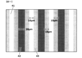
- FIG. 3 is a plan view showing an example of the arrangement and dimensions of a light-transmitting part, a light-shielding part, and a semi-light-transmitting part in a halftone photomask used for evaluating halftone characteristics.
- FIG. 2 is a plan view showing an example of the arrangement and dimensions of a thick film part, an opening part, and a thin film part of an organic EL display used for evaluating light emission characteristics.
- display devices that are the first and second aspects of the present invention will be described.
- the display device of the present invention refers to the display device that is the first aspect and the second aspect of the present invention, and the cured product obtained by curing the photosensitive composition that is the third aspect of the present invention, which will be described later.
- This is a description of a display device including the following.
- a display device of a specific aspect it will be described as a display device of a first aspect.
- a plane in plan view refers to a plane horizontal to a substrate, which will be described later.
- planar view refers to the xy-axis viewed from the z-axis direction, where the plane horizontal to the substrate is the xy-axis plane, and the direction orthogonal to the xy-axis plane is the z-axis direction.
- a plan view of the light extraction side of the display device Note that when focusing on a specific member in a plan view, it is assumed that another member overlapping the specific member is seen through. If the substrate is not flat, a plane horizontal to an arbitrary pixel portion, which will be described later, is defined as an xy plane.
- overlapping means directly or indirectly overlapping in the z-axis direction.
- the average value of pattern dimensions can be calculated as the average value obtained by measuring pattern dimensions at 30 points using an optical microscope or a scanning electron microscope (hereinafter referred to as "SEM").
- the maximum and minimum values of the pattern dimensions can be similarly calculated as the maximum and minimum values obtained by measuring the pattern dimensions at 30 points using an optical microscope or SEM.
- the main chain of the resin refers to the chain with the longest chain length among the chains constituting the resin including structural units.
- the side chain of a resin refers to a chain that is branched from or bonded to the main chain and has a chain length shorter than the main chain among the chains constituting the resin containing structural units.
- the terminus of the resin refers to a structure that seals the main chain, and is, for example, a structure derived from an end-capping agent.
- a hydrocarbon group or alkylene group containing a "** bond” or "** group” refers to a hydrocarbon group or alkylene group to which a "** bond" or "** group” is bonded, or a "* Refers to at least two hydrocarbon groups or at least two alkylene groups connected by a *bond or a ** group.
- a display device is a display device having an organic layer including a substrate, a first electrode, a second electrode, a pixel dividing layer, and a light emitting layer,
- the pixel dividing layer contains a (D-DL) colorant, and the optical density at the wavelength of visible light per 1 ⁇ m of film thickness of the pixel dividing layer is 0.5 to 3.0, In plan view, it has a plurality of pixel parts, Measured by time-of-flight secondary ion mass spectrometry at a depth of 3 nm from the surface of the first electrode on the side in contact with the organic layer including the light-emitting layer in the pixel portion.
- the detection intensity of sulfur ions (S ⁇ ) is defined as (S Dep/Anode ) counts
- the detection intensity of chlorine ion (Cl ⁇ ) is defined as (Cl Dep/Anode ) counts
- the display device satisfies the relationship expressed by general formula (SA-1) and/or the relationship expressed by general formula (XA-1). 2 ⁇ (S Dep/Anode ) ⁇ 200 (SA-1) 2 ⁇ (X Dep/Anode ) ⁇ 200 (XA-1).
- the display device of the present invention can have both excellent light emission characteristics that can be driven at a low voltage and high reliability of the light emitting element.
- the higher the detection intensity of sulfur ions, chlorine ions, and bromine ions on the surface of the first electrode in contact with the organic layer including the light emitting layer the more likely the surface is modified by these elements on the surface of the first electrode.
- the polarization structure and charge balance on the first electrode in an organic EL display can be controlled. It is estimated that this suppresses ion migration and electromigration caused by metal impurities and ionic impurities that adversely affect light-emitting characteristics, thereby achieving high reliability of the light-emitting element. Furthermore, it is estimated that the light-emitting element has a highly reliable effect by suppressing migration and aggregation of the metal in the first electrode. Furthermore, the effect of high reliability of the light emitting element is achieved.
- a display device is a display device having an organic layer including a substrate, a first electrode, a second electrode, a pixel dividing layer, and a light emitting layer,
- the pixel dividing layer contains a (D-DL) colorant, and the optical density at the wavelength of visible light per 1 ⁇ m of film thickness of the pixel dividing layer is 0.5 to 3.0
- the pixel dividing layer contains one or more types selected from the group consisting of the following (I1a-DL) compounds, (I1b-DL) compounds, (I2a-DL) compounds, and (I2b-DL) compounds, (I1a-DL) compound and (I2a-DL) compound have the following (I-Ia) structure,
- the (I1b-DL) compound and the (I2b-DL) compound have the following (I-Ib) structure, which is a display device.
- (I1a-DL) Compound from a thiol structure-containing compound, a sulfide structure-containing compound, a disulfide structure-containing compound, a sulfoxide structure-containing compound, a sulfone structure-containing compound, a sultone structure-containing compound, a thiophene structure-containing compound, and a sulfonic acid structure-containing compound
- One or more types of compounds selected from the group consisting of (I1b-DL) Compound One or more types selected from the group consisting of sulfide ion structure, hydrogen sulfide ion structure, sulfate ion structure, and hydrogen sulfate ion structure as anion species has, and A compound (I2a-DL) having an ammonium ion structure, a primary ammonium ion structure, a secondary ammonium ion structure, a tertiary ammonium ion structure, or a quaternary ammonium
- the content of sulfur element in the pixel dividing layer is 0.01 to 500 ppm by mass (1b-DL)
- the total content of sulfide ions, hydrogen sulfide ions, sulfate ions, and hydrogen sulfate ions in the pixel division layer is 0.01 to 1,000 ppm by mass (2a-DL)
- the total content of chlorine element and bromine element in the pixel division layer is 0.01 to 500 ppm by mass (2b-DL)
- the total content of chloride ions and bromide ions in the pixel dividing layer is 0.01 to 1,000 ppm by mass.
- the display device of the present invention can have both excellent light-emitting characteristics that can be driven at a low voltage and high reliability of the light-emitting element.
- the light emitting element has a highly reliable effect by suppressing migration and aggregation of the metal in the first electrode.
- the display device of the present invention has a substrate.
- the substrate preferably contains silicon dioxide or dialuminum trioxide, and more preferably a glass substrate, a quartz substrate, a crystal substrate, or a sapphire substrate.
- the substrate is preferably a flexible substrate from the viewpoints of improved flexibility, improved bendability, and improved shape freedom of the display device (curved shape, folded shape, etc.).
- the flexible substrate is preferably a substrate containing carbon as a main component from the viewpoint of improving the adhesion between the cured film of the present invention and the substrate and improving the bendability.
- the main component element in the flexible substrate refers to the element that is contained in the largest amount among the constituent elements of the flexible substrate.
- the flexible substrate is preferably a polyimide substrate, a polyethylene terephthalate substrate, a cycloolefin polymer substrate, a polycarbonate substrate, or a cellulose triacetate substrate, and from the viewpoint of improving bendability, a polyimide substrate is more preferable.
- the display device of the present invention preferably has a structure in which a pixel division layer, which will be described later, is laminated on a flexible substrate.
- the display device of the present invention is preferably a flexible display device, and preferably has a curved display portion, a display portion including an outwardly folded surface, or a display portion including an inwardly folded surface.
- the flexible display device is preferably a flexible organic EL display, a flexible quantum dot display, or a flexible micro LED display, and more preferably a flexible organic EL display.
- the display device of the present invention has a first electrode and a second electrode.
- a transparent electrode and a non-transparent electrode as the first electrode and the second electrode, it is possible to extract light emitted from an organic layer including a light emitting layer to be described later to one side.
- Transparent electrodes and non-transparent electrodes are required to have excellent electrical properties. When a transparent electrode or a non-transparent electrode is used as an anode, it is required to have multiple properties such as being able to efficiently inject holes, while when being used as a cathode, it is required to be able to inject electrons efficiently.
- a display device with a bottom emission type configuration has a transparent electrode as the first electrode and a non-transparent electrode as the second electrode.
- a display device having a top emission type configuration has a non-transparent electrode as the first electrode and a transparent electrode as the second electrode.
- the display device having a bottom emission type structure is preferably an organic EL display having a bottom emission type structure.
- the display device having a top emission type configuration is preferably an organic EL display having a top emission type configuration.
- a transparent electrode refers to an electrode having a transmittance of 30% or more at a wavelength of 550 nm.
- a non-transparent electrode refers to an electrode whose transmittance at a wavelength of 550 nm is less than 30%.
- the transmittance is measured using the transmittance at a wavelength of 550 nm when the electrode has a multilayer structure, and the electrode is classified as a transparent electrode or a non-transparent electrode.
- the first electrode, which is a non-transparent electrode has a multilayer structure.
- the first electrode, which is a non-transparent electrode may have a multilayer structure, and the first electrode may have a base layer on the substrate side that improves adhesion and corrosion resistance, and a reflection adjustment layer that adjusts reflectance.
- the electrode has a single-layer structure, transparent or non-transparent in the transparent conductive oxide film layer, non-transparent conductive layer, non-transparent conductive metal layer, transparent conductive layer, and transparent conductive metal layer described below means: Similarly to the above, it means that the transmittance at a wavelength of 550 nm is 30% or more or less than 30%. On the other hand, when the electrode has a multilayer structure, it is said to be transparent if the overall transmittance at a wavelength of 550 nm is 30% or more, and it is called non-transparent if the transmittance of even one of the layers constituting the multilayer structure is less than 30%.
- the electrode comprising the multilayer structure is a non-transparent electrode.
- each layer constituting the multilayer structure preferably has a transmittance of 70% or more at a wavelength of 550 nm.
- the display device of the present invention has a plurality of first electrode parts in a plan view.
- a plan view of the first electrode described above corresponds to the first electrode portion.
- the display device of the present invention has a second electrode part in a plan view.
- a plan view of the second electrode described above corresponds to the second electrode portion.
- the display device of the present invention has a plurality of second electrode parts. The shape of the first electrode part when the display device of the present invention has a plurality of first electrode parts, and the shape of the second electrode part when the display device of the present invention has a plurality of second electrode parts are closed.
- a polygon a shape in which at least some of the sides and/or vertices of a closed polygon are replaced with circular arcs, or a closed shape formed of circular arcs are preferable.
- Examples and preferred descriptions of closed polygons, shapes in which at least some of the sides and/or vertices of a closed polygon are replaced with circular arcs, and closed shapes formed of circular arcs are as described below. .
- the display device of the present invention preferably has a transparent conductive oxide film layer on the outermost layer on the light emitting layer side of the first electrode, and the display device preferably has a transparent conductive oxide film layer containing In, Sn, Zn, Al, or Ga as a main component. It is more preferable to have a transparent conductive oxide film layer, and it is even more preferable to have a transparent conductive oxide film layer containing indium as a main component element.
- the main component element in the transparent conductive oxide film layer refers to an element other than oxygen that is contained in the largest amount among the constituent elements of the transparent conductive oxide film layer.
- the transparent conductive oxide film layer containing In, Sn, Zn, Al, or Ga as a main component is preferably ITO or IZO, more preferably ITO, from the viewpoint of driving the light emitting characteristics at a low voltage and improving the light emission brightness.
- the transparent conductive oxide film layer is preferably an amorphous transparent conductive oxide film layer from the viewpoint of driving the light emitting characteristics at a low voltage and improving the reliability of the light emitting device.
- a neutral oxide film layer is more preferable.
- the transparent conductive oxide film layer is preferably a polycrystalline transparent conductive oxide film layer, and more preferably a polycrystalline transparent conductive oxide film layer containing indium as a main component element.
- these transparent conductive oxide film layers are provided on the outermost layer of the first electrode on the light emitting layer side. It is preferable to have.
- the first electrode has a single layer structure or a multilayer structure. When the first electrode has a single layer structure, the first electrode is preferably a transparent electrode.
- the first electrode When the first electrode has a multilayer structure, the first electrode is a transparent electrode or a non-transparent electrode.
- the first electrode When the first electrode is used as an anode, the first electrode is preferably ITO or IZO, more preferably ITO, from the viewpoint of driving the light emitting characteristics at a low voltage and improving the light emission brightness.
- the first electrode When the first electrode is a transparent electrode, it is preferable to adjust the film thickness of the first electrode to adjust the transmittance at a wavelength of 550 nm.
- the first electrode When the first electrode is a non-transparent electrode with a single layer structure, the first electrode is a non-transparent conductive layer. When the first electrode is a non-transparent electrode with a multilayer structure, the first electrode has a non-transparent conductive layer. It is preferable that at least one layer other than the outermost layer on the light-emitting layer side of the first electrode is a non-transparent conductive layer. Regardless of whether the first electrode is a non-transparent electrode and has a single-layer structure or a multi-layer structure, the non-transparent conductive layer is preferably a non-transparent conductive metal layer containing a metal element.
- the non-transparent conductive metal layer is made of Ag, Cu, Au, etc., from the viewpoints of low voltage driving of the light emitting characteristics, improvement of luminescence brightness, improvement of reliability of the light emitting element, and improvement of corrosion resistance. , Ti, Al, Ni, Mo, or Cr as the main component, more preferably Ag, Cu, Au, Ti, or Al as the main component, and silver or copper as the main component. It is more preferable to include it as an element.
- the non-transparent conductive metal layer further contains In, Sn, Zn, Al, Ga, Pd, Cu, Bi, Nd, Ni, Mn, Na, K, Mg, Ca, C, as elements different from the main component elements.
- the main component element in the non-transparent conductive metal layer refers to the element that is contained in the largest amount among the constituent elements of the non-transparent conductive metal layer.
- the first electrode is a non-transparent electrode, it is preferable to adjust the thickness of the first electrode to adjust the transmittance at a wavelength of 550 nm.
- the display device of the present invention preferably has a transparent conductive metal layer on the outermost layer on the light emitting layer side of the second electrode, and has a transparent conductive metal layer containing Li, Mg, Ag, Cu, Au, Ti, or Al as a main component. It is more preferable to have a transparent conductive metal layer containing magnesium or silver as a main component element.
- the main component element in the transparent conductive metal layer refers to the element that is contained in the largest amount among the constituent elements of the transparent conductive metal layer.
- the transparent conductive metal layer containing Li, Mg, Ag, Cu, Au, Ti, or Al as a main component is preferably LiAg or MgAg, and more preferably MgAg, from the viewpoint of improving luminance.
- the second electrode whether the second electrode has a multilayer structure and is a transparent electrode or a non-transparent electrode, these transparent conductive metal layers are provided on the outermost layer of the second electrode on the light emitting layer side. It is preferable to have.
- the transparent conductive metal layer or the non-transparent conductive metal layer is made of Li, Mg, Ag, Cu, Au, Ti, or Al, from the viewpoint of improving luminance and reliability of the light emitting element. It is more preferable to have a transparent conductive metal layer containing as a main component element. From the viewpoint of improving luminance, the transparent conductive metal layer is preferably LiAg or MgAg, and more preferably MgAg.
- the second electrode is a transparent electrode or a non-transparent electrode, it is preferable to adjust the thickness of the second electrode to adjust the transmittance at a wavelength of 550 nm.
- the first electrode is a non-transparent electrode with a multilayer structure, and the first electrode has a non-transparent conductive metal layer, from the viewpoint of driving the light emission characteristics at a low voltage and improving the light emission brightness. It is preferable that at least one layer of the first electrode other than the outermost layer on the light emitting layer side has a non-transparent conductive metal layer containing silver or copper as a main component element.
- the first electrode is formed of a transparent conductive oxide film layer from the viewpoint of driving the light emitting characteristics at a low voltage and improving the reliability of the light emitting element. and a non-transparent conductive metal layer, and preferably has a transparent conductive oxide film layer containing indium as a main component on the outermost layer on the light-emitting layer side of the first electrode.
- the first electrode is a non-transparent electrode with a multilayer structure, and the first electrode is a transparent conductive electrode, from the viewpoint of lower voltage driving of the light emission characteristics, improvement of the luminance, and improvement of the reliability of the light emitting element.
- the first electrode has an amorphous transparent conductive oxide film layer containing indium as a main component on the outermost layer on the light emitting layer side of the first electrode. It is preferable that at least one layer of the electrode other than the outermost layer on the light emitting layer side has a non-transparent conductive metal layer containing silver or copper as a main component, and has a top emission type structure.
- the silver or copper contained in the non-transparent conductive metal layer has excellent low resistance characteristics, the effects of lower voltage driving of the light emitting characteristics and improvement of the light emission brightness are remarkable. Further, it is estimated that the adjustment of the work function difference by the indium contained in the transparent conductive oxide film layer will significantly improve the effect of lower voltage driving of the light emitting characteristics and improvement of the reliability of the light emitting element.
- the amorphous transparent conductive oxide film layer suppresses the occurrence of defects, and the top-emission structure reduces stray light and scattered light inside the device, making it possible to increase the driving voltage to ensure luminance. It is estimated that the effect of improving the reliability of the light-emitting element will be significant because it can be suppressed.
- the outermost amorphous conductive oxide film layer is easily surface modified by sulfur elements, chlorine elements, and bromine elements, and the light emitting characteristics can be driven at lower voltages by adjusting the work function difference, and the light emitting element can be It is estimated that the effect of improving reliability will be significant.
- the light extraction efficiency is improved due to the high reflectance characteristics of these metals, so it is possible to lower the voltage driving of the light emitting characteristics and improve the light extraction efficiency. It is estimated that the effect of improving luminance will be significant. Similarly, since conductivity is improved due to the low resistivity characteristic of these metals, it is estimated that the effects of lower voltage driving of the light emitting characteristics and improvement of light emission brightness will be significant.
- An amorphous transparent conductive oxide film layer and a non-transparent conductive metal layer containing silver or copper as the main element enable lower voltage driving of light emitting characteristics, improved reliability of light emitting elements, improved luminance, and light extraction. Since the effect of improving efficiency is significant, it is particularly suitable for display devices having a top emission type configuration.
- the total content ratio of the silver element and the copper element in the non-transparent conductive metal layer containing silver or copper as a main component element in the first electrode is determined by the low voltage drive of the light emitting characteristics due to high reflectance and low resistivity. From the viewpoint of improving the luminance and emission brightness, the content is preferably 95% by mass or more, more preferably 96% by mass or more, and even more preferably 97% by mass or more. On the other hand, the total content ratio of the silver element and the copper element is preferably 99.5% by mass or less, and 99% by mass or less, from the viewpoint of low-voltage driving of the luminescent characteristics and improvement of luminescence brightness due to high reflectance and low resistivity. is more preferable, and even more preferably 98.5% by mass or less.
- the non-transparent conductive metal layer containing silver as a main component element in the first electrode preferably further contains copper and/or palladium as an element different from the main component element, and more preferably contains copper and palladium. preferable. Further, the non-transparent conductive metal layer containing copper as a main component element in the first electrode preferably further contains silver and/or palladium as an element different from the main component element, and preferably contains silver and palladium. is more preferable.
- the conductivity of the first electrode is improved, so it is estimated that the effects of lower voltage driving of the light emitting characteristics and improvement of the light emission brightness become more significant. Furthermore, since the heat resistance and oxidation resistance of the first electrode are significantly improved, it is estimated that the effect of improving the reliability of the light emitting element will be significant.
- the total content ratio of the copper element and the palladium element in the non-transparent conductive metal layer containing silver as the main component element in the first electrode is determined by the following: From the viewpoint of improving reliability, the content is preferably 0.1% by mass or more, more preferably 0.5% by mass or more, and even more preferably 1.0% by mass or more. On the other hand, the total content ratio of the copper element and the palladium element is preferably 5% by mass or less, more preferably 4% by mass or less, from the viewpoint of driving the light emission characteristics at a low voltage, improving the luminance brightness, and improving the reliability of the light emitting element. It is preferably 3% by mass or less, and more preferably 3% by mass or less.
- the total content ratio of silver element and palladium element in the non-transparent conductive metal layer containing copper as a main component element in the first electrode is determined by the total content ratio of silver element and palladium element, which contributes to low voltage driving of the light emission characteristics, improvement of light emission brightness, and light emission.
- the content is preferably 0.1% by mass or more, more preferably 0.5% by mass or more, and even more preferably 1.0% by mass or more.
- the total content ratio of the silver element and the palladium element is preferably 5% by mass or less, more preferably 4% by mass or less, from the viewpoints of driving the light emitting characteristics at a lower voltage, improving the luminance brightness, and improving the reliability of the light emitting element. It is preferably 3% by mass or less, and more preferably 3% by mass or less.
- the first electrode is a non-transparent electrode with a multilayer structure
- the first electrode has a transparent conductive oxide film layer and a non-transparent conductive metal layer
- the first electrode has a transparent conductive oxide film layer and a non-transparent conductive metal layer
- the outermost layer has an amorphous transparent conductive oxide film layer containing indium as a main component element, and at least one layer other than the outermost layer on the light emitting layer side of the first electrode contains silver or copper as a main component.
- the non-transparent conductive metal layer containing silver or copper as a main component element in the first electrode further contains In, Sn, Zn, Al, Ga, It is preferable to include one or more selected from the group consisting of Bi, Nd, Ni, Mn, Na, K, Mg, Ca, C, and Si, including In, Sn, Al, Na, K, Mg, Ca, It is more preferable to include one or more types selected from the group consisting of and Si, and it is even more preferable to include one or more types selected from the group consisting of Na, K, Mg, and Ca.
- the non-transparent conductive metal layer containing silver as a main element in the first electrode contains copper and/or palladium, and preferably further contains these elements.
- the non-transparent conductive metal layer containing copper as a main component element in the first electrode contains silver and/or palladium, and preferably further contains these elements.
- the total content ratio of each element, C and Si is preferably 0.1% by mass or more, more preferably 0.5% by mass or more, from the viewpoint of driving the light emission characteristics at a low voltage and improving the luminance brightness.
- the total content ratio of each element of In, Sn, Zn, Al, Ga, Bi, Nd, Ni, Mn, Na, K, Mg, Ca, C, and Si is the From the viewpoint of improving luminance, the content is preferably 3% by mass or less, more preferably 2% by mass or less.
- the display device of the present invention has a pixel dividing layer.
- the pixel division layer is a layer that divides adjacent pixel parts and defines the area of each pixel part.
- the pixel dividing layer is a layer that divides a region on the first electrode. Note that when the display device of the present invention has a pixel size control layer described later, the pixel size control layer also divides adjacent pixel parts, and the pixel size control layer is a layer that defines the area and size of each pixel part. Become.
- the pixel dividing layer is preferably a cured film obtained by curing a photosensitive composition, more preferably a cured film obtained by curing a photosensitive composition containing a colorant, and even more preferably a cured film obtained by curing a photosensitive composition containing a black agent. It is preferable that the pixel division layer is formed so as to partially overlap with the above-described first electrode. With such a configuration, the first electrode and the second electrode in any pixel can be insulated, and it is possible to suppress the pixel from turning off due to a short circuit between the first electrode and the second electrode. Further, the first electrode in any pixel can be insulated from the first electrode in an adjacent pixel, and it is possible to suppress the pixel from turning off due to a short circuit between the first electrodes.
- the pixel dividing layer is preferably black at the wavelength of visible light due to the coloring of components such as resin in the photosensitive composition, and in addition to the coloring of components such as resin, thermal color formers and/or oxidative color formers, etc. It is more preferable that the color is black.
- the pixel dividing layer is more preferably black due to coloring with a plurality of colorants, and even more preferably black due to coloration with a thermal color former and/or an oxidative color former in addition to the coloration with a plurality of colorants. preferable. It is particularly preferred that the pixel dividing layer is black with a black agent. Note that colored means red, orange, yellow, green, blue, or purple.
- the display device of the present invention has a pixel division layer portion having a plurality of openings in plan view.
- a plan view of the above-mentioned pixel division layer corresponds to the pixel division layer portion.
- the shape of the pixel portion which will be described later, is preferably similar to or similar to the shape of the opening of the pixel dividing layer, and is preferably the same as the shape of the opening of the pixel dividing layer. More preferred.
- the shape of the pixel section described below is preferably similar to or similar to the shape of the opening of the pixel size control layer section. It is more preferable that the shape of the opening is the same as that of the opening of the pixel size control layer.
- the shape of the pixel portion is preferably a closed polygon, a shape in which at least some of the sides and/or vertices of a closed polygon are replaced with circular arcs, or a closed shape formed by circular arcs.
- closed polygons include triangles, equilateral triangles, isosceles triangles, right triangles, quadrilaterals, squares, rhombuses, rectangles, trapezoids, right trapezoids, and parallelograms.
- Examples of shapes in which at least some of the sides and/or vertices of a closed polygon are replaced with circular arcs include triangles, equilateral triangles, isosceles triangles, right triangles, quadrilaterals, squares, rhombuses, rectangles, trapezoids, and right trapezoids. , or a shape in which at least some of the sides and/or vertices of a parallelogram are replaced with circular arcs.
- Examples of the closed shape formed by a circular arc include a circle, a perfect circle, and an ellipse.
- the shape of the pixel portion is preferably a quadrilateral, a square, a rhombus, or a rectangle; a shape in which at least some of the sides and/or vertices of a quadrilateral, square, rhombus, or rectangle are replaced with arcs, or a circle or a perfect circle.
- the shape of the pixel part is a closed polygon, or at least some of the sides and/or vertices of the closed polygon are replaced with circular arcs from the viewpoints of suppressing reflection of external light, driving the light emitting characteristics at a low voltage, and improving the light emission brightness.
- a rounded shape is preferred.
- the light emitted from the light emitting element becomes asymmetrical as surface light emission, and is strengthened by reflection and interference between the first electrode and the second electrode, so the light emission It is estimated that the effects of lower voltage driving characteristics and improved luminance will be noticeable.
- the scattering of incident external light on the surface of the pixel dividing layer part becomes asymmetrical, and the reflection between the first electrode and the second electrode becomes asymmetric. It is estimated that the effect of suppressing reflection of external light becomes significant because it is weakened by interference.
- the shape of the opening in the overcoat layer is preferably a closed polygon, a closed polygon with at least some of its sides and/or vertices replaced with circular arcs, or a closed polygon formed by circular arcs. . Examples and preferred descriptions of closed polygons, shapes in which at least some of the sides and/or vertices of a closed polygon are replaced with circular arcs, and closed shapes formed of circular arcs are as described above.
- the shape of the color filter layer section which will be described later and overlaps with the pixel section, is preferably similar to or similar to the shape of the pixel section.
- the shape of the opening in the black matrix layer section which will be described later, overlaps with the pixel section, and preferably has a similar shape or a similar shape to the shape of the pixel section.
- the shape of the color filter layer is preferably similar to or similar to the shape of the opening of the black matrix layer. It is more preferable that the shape of the pixel part, the shape of the color filter layer part, and the shape of the opening part of the black matrix layer part are all similar or similar shapes.
- any one of the shapes of the pixel portion, the shape of the color filter layer portion, and the shape of the opening portion of the black matrix layer portion may not be similar or similar shapes.
- the shape of the pixel section, the shape of the color filter layer section, and the shape of the opening section of the black matrix layer section do not have to be similar or similar to each other.
- FIG. 4 is a plan view showing an example of the shape of the pixel section, the shape of the color filter layer section, and the shape of the opening section of the black matrix layer section.
- the shape of the pixel portion, the shape of the opening in the pixel dividing layer, the shape of the opening in the pixel size control layer (described later), the shape of the spacer layer (described later), the shape of the color filter layer (described later), the black matrix layer (described later) The pattern dimensions in the major axis direction and the pattern dimensions in the minor axis direction in the shape of the opening of the overcoat layer section, the shape of the overcoat layer section described below, and the shape of the opening of the overcoat layer section described below will be described below.
- the pattern dimension in the major axis direction refers to the length of the longest straight line among the straight lines that symmetrically divide the closed polygon into two.
- the pattern dimension in the short axis direction refers to the length of the longest straight line among the straight lines in the direction perpendicular to the long axis direction.
- the pattern dimension in the long axis direction means that at least some of the sides and/or vertices of the closed polygon are replaced with circular arcs.
- the pattern dimension in the short axis direction refers to the length of the longest straight line among the straight lines in the direction perpendicular to the long axis direction.
- the pattern dimension in the major axis direction refers to the length of the longest straight line among the straight lines that symmetrically divide the closed shape formed by a circular arc into two.
- the pattern dimension in the short axis direction refers to the length of the longest straight line among the straight lines in the direction perpendicular to the long axis direction.
- the pattern dimension in the major axis direction refers to the diameter of the longest circle.
- the pattern dimension in the short axis direction refers to the diameter of a circle in the direction perpendicular to the long axis direction.
- the pattern dimensions of the openings in the pixel dividing layer section and the openings in the pixel size control layer section described below refer to the length from bottom to bottom of the openings.
- the average value of the pattern dimensions in the long axis direction of the openings in the pixel dividing layer section or the openings in the pixel size control layer section is used to suppress reflection of external light, lower voltage driving of light emitting characteristics, improve luminance, and improve reliability of light emitting elements.
- the thickness is preferably 5.0 ⁇ m or more, more preferably 6.0 ⁇ m or more, even more preferably 7.0 ⁇ m or more, even more preferably 8.0 ⁇ m or more, and particularly preferably 10.0 ⁇ m or more.
- the average value of the pattern dimensions in the long axis direction of the openings of the pixel dividing layer section or the openings of the pixel size control layer section described below is preferably 50.0 ⁇ m or less from the viewpoint of suppressing reflection of external light and improving luminance. , more preferably 40.0 ⁇ m or less, and even more preferably 35.0 ⁇ m or less.
- the average value of the pattern dimensions in the long axis direction of the openings in the pixel dividing layer section or the openings in the pixel size control layer section can be used to suppress reflection of external light, lower voltage driving of the light emitting characteristics, improve luminance, and improve the light emitting element.
- the thickness is preferably 30.0 ⁇ m or less, more preferably 25.0 ⁇ m or less, even more preferably 20.0 ⁇ m or less, even more preferably 17.0 ⁇ m or less, and particularly preferably 15.0 ⁇ m or less.
- the pattern dimension in the long axis direction of the pixel section refers to the length from bottom to bottom in the pixel section.
- the pattern dimension in the long axis direction of the pixel part is (CD) ⁇ m
- the pattern dimension in the long axis direction of the opening of the pixel division layer part or the opening of the pixel size control layer part corresponding to the pixel part is (DL).
- the dimensional difference ( ⁇ CD-DL) ⁇ m between (CD) ⁇ m and (DL) ⁇ m is preferably ⁇ 2.0 ⁇ m or more, more preferably ⁇ 1.5 ⁇ m or more, and still more preferably ⁇ 1.0 ⁇ m or more.
- the dimensional difference ( ⁇ CD-DL) ⁇ m between (CD) ⁇ m and (DL) ⁇ m is preferably 2.0 ⁇ m or less, more preferably 1.5 ⁇ m or less, even more preferably 1.0 ⁇ m or less, and 0.5 ⁇ m or less. is even more preferable, and 0.2 ⁇ m or less is particularly preferable. It is most preferable that the pattern size in the long axis direction of the pixel portion is the same as the pattern size in the long axis direction of the opening of the pixel dividing layer portion or the opening of the pixel size control layer portion corresponding to the pixel portion.
- the display device of the present invention further includes a pixel size control layer.
- the pixel size control layer is a layer that is in contact with both the pixel division layer and the pixel section and adjusts the size of the area of each pixel section.
- the pixel size control layer is preferably a layer that adjusts the size of the area on the first electrode divided by the pixel division layer.
- the pixel size control layer is preferably a cured film obtained by curing a photosensitive composition. It is preferable that the pixel size control layer is formed so as to partially overlap with the above-described first electrode.
- the pattern dimensions of the openings serving as pixel portions can be controlled with high precision, so that the effect of improving the pattern dimension uniformity becomes remarkable.
- the pattern dimensions of the pixel section, the pattern dimensions of the color filter layer section, and the pattern dimensions of the opening section of the black matrix layer section can be controlled with high precision, suppressing the reflection of external light, lowering the voltage driving of the light emitting characteristics, and increasing the luminance. and the effect of improving the reliability of the light emitting element becomes remarkable.
- the display device of the present invention further includes a pixel size control layer portion having a plurality of openings in plan view.
- “covering” means that at least a portion thereof directly overlaps in the z-axis direction.
- a plan view of the above-mentioned pixel size control layer corresponds to the pixel size control layer section.
- FIG. 3 shows a schematic cross-sectional view and a plan view of an example of a display device including a pixel dividing layer and a pixel size control layer having a stepped shape.
- the display device of the present invention further includes a spacer layer.
- the spacer layer is a layer located above and/or below the pixel division layer. By having the spacer layer, even when the pixel dividing layer does not have a step shape, it is possible to provide a function corresponding to the thick film portion when the pixel dividing layer has a step shape.
- the spacer layer preferably includes a spacer layer above the pixel dividing layer and/or a lower spacer layer located below the pixel dividing layer.
- the spacer layer is preferably a cured film obtained by curing a photosensitive composition.
- the spacer layer is formed on a portion of the pixel division layer.
- the contact area between the pixel division layer and the vapor deposition mask when forming the organic layer including the light emitting layer can be reduced. Therefore, by suppressing damage to the pixel division layer, the effect of suppressing a decrease in panel yield and improving the reliability of light emitting elements becomes significant.
- the display device of the present invention further includes a spacer layer portion in a plan view.
- a plan view of the spacer layer described above corresponds to the spacer layer portion.
- the shape of the spacer layer is preferably a closed polygon or a shape in which at least some of the sides and/or vertices of the closed polygon are replaced with circular arcs.
- the pixel dividing layer contains a (DDL) colorant.
- incident external light can be blocked by the pixel division layer, so that the effect of suppressing reflection of external light becomes significant.
- the light-shielding properties of the pixel dividing layer at visible light wavelengths and wavelengths in the ultraviolet region, outgassing from the pixel dividing layer, etc. is suppressed, and deterioration of the light emitting element is suppressed, so the reliability of the light emitting element is improved. It becomes noticeable.
- the (D-DL) colorant in the pixel dividing layer is preferably a black agent and/or a colorant mixture of two or more colors.
- the (D-DL) colorant in the pixel dividing layer preferably contains a pigment and/or a dye, more preferably a pigment and a dye.
- the pixel dividing layer contains a (D-DL) colorant, and that the spacer layer satisfies at least one of the following conditions (1) to (3).
- the spacer layer more preferably satisfies at least one of the conditions (1) and (3) below, and even more preferably satisfies at least the condition (1) below.
- the spacer layer does not contain the (D-DL) colorant.
- the spacer layer contains the (D-DL) colorant, and the optical density at the wavelength of visible light per 1 ⁇ m of the spacer layer thickness is 0.
- the spacer layer contains a compound having a (C2x-DL) carboxylic acid ester structure containing an indene structure and/or a sulfonic acid aryl ester structure containing an indene structure.
- the pixel dividing layer and the spacer layer are formed by a two-layer film formation method using photosensitive compositions with different compositions, or the spacer layer is formed using a positive photosensitive composition. It is formed from a composition.
- the method of forming a two-layer film since the openings of the first layer come into contact with the alkaline developer again, the generation of residue at the openings of the pixel dividing layer section or the openings of the pixel size control layer section is suppressed. It is estimated that the effects of lower voltage driving of light emitting characteristics and improvement of light emission brightness will be significant.
- the first pixel dividing layer is not halftone exposed using a halftone photomask, but in the case of a negative type, photocuring is sufficiently progressed by fulltone exposure, and the solubility in alkaline developer is significantly reduced. are doing. Therefore, the surface of the first pixel division layer is a smooth film surface with little roughness, and it is estimated that the scattering of the incident external light is suppressed, so that the effect of suppressing reflection of external light becomes significant.
- the spacer layer is formed of a positive photosensitive composition, alkali dissolution in the openings is promoted by exposure to light, and the generation of development residue is suppressed. It is estimated that the effect will be significant.
- the (D-DL) colorant in the spacer layer is preferably a black agent and/or a colorant mixture of two or more colors.
- the (D-DL) colorant in the spacer layer preferably contains a pigment and/or a dye, more preferably a pigment and a dye.
- the (D-DL) colorant in the pixel dividing layer etc. preferably contains a black pigment and/or a mixture of two or more colored pigments from the viewpoint of suppressing reflection of external light and improving reliability of the light emitting device.
- the (D-DL) colorant in the pixel dividing layer etc. preferably contains a black dye and/or a mixture of two or more colored dyes from the viewpoint of suppressing external light reflection and improving the reliability of the light emitting device.
- the (D-DL) colorant in the pixel dividing layer etc. is preferably the (D) colorant described below.
- the pixel dividing layer etc. contain a black pigment.
- the incident external light can be blocked by the pixel division layer or the like, so that the effect of suppressing reflection of external light becomes significant.
- the light-shielding properties of the pixel dividing layer, etc. at visible light wavelengths and wavelengths in the ultraviolet region, outgassing from the pixel dividing layer, etc. is suppressed, and deterioration of the light emitting element is suppressed, resulting in the effect of improving the reliability of the light emitting element. becomes noticeable.
- the pixel dividing layer etc. contains an organic black pigment and/or a mixture of two or more colored pigments
- the organic black pigment includes one or more types selected from the group consisting of benzofuranone black pigments, perylene black pigments, and azo black pigments, It is preferable that the colored pigment mixture of two or more colors contains pigments of two or more colors selected from the group consisting of red, orange, yellow, green, blue, and violet.
- the organic black pigment more preferably contains a benzofuranone-based black pigment and/or a perylene-based black pigment, and even more preferably contains a benzofuranone-based black pigment.
- Colored pigment mixtures of two or more colors include anthraquinone pigments, diketopyrrolopyrrole pigments, perylene pigments, isoindoline pigments, isoindolinone pigments, imidazolone pigments, quinacridone pigments, pyranthrone pigments, and phthalocyanine pigments. , indanthrone pigments, and dioxazine pigments, and one or more pigments selected from the group consisting of perylene pigments, imidazolone pigments, and indanthrone pigments. It is more preferable to include the above pigments.
- the benzofuranone black pigment has at least two benzofuran-2(3H)-one structures that may share a benzene ring or at least two benzofuran-3(2H)-one structures that may share a benzene ring. is preferable, and it is more preferable to include a compound having a structure represented by either general formula (161) or general formula (162), a geometric isomer thereof, a salt thereof, or a salt of a geometric isomer thereof. .
- the pixel dividing layer etc. contains an organic black pigment and/or a mixture of two or more colored pigments
- the pixel dividing layer etc. contains a benzofuranone black pigment
- the benzofuranone black pigment is It is preferable to include a compound having a structure represented by either general formula (161) or general formula (162), a geometric isomer thereof, a salt thereof, or a salt of a geometric isomer thereof.
- the benzofuranone black pigment in the pixel dividing layer and the like is preferably a benzofuranone black pigment described below.
- benzofuranone black pigment in the pixel dividing layer etc. promotes a surface modification effect on the surface of the first electrode on the light emitting layer side corresponding to the opening of the pixel dividing layer or the opening of the pixel size control layer. Ru. Therefore, it is thought that adjustment of the work function difference promotes lower voltage driving of the light emitting characteristics. As a result, it is estimated that the effect of improving light emission brightness when driven at the same voltage becomes significant.
- benzofuranone black pigments have superior light-shielding properties per unit mass of the pigment compared to general organic pigments, and therefore have remarkable effects of suppressing reflection of external light and improving reliability of light-emitting devices.
- benzofuranone black pigments have excellent insulation properties and low dielectric properties compared to general organic pigments and inorganic pigments, and therefore have a remarkable effect of improving the reliability of light emitting devices.
- R 341 to R 344 each independently represent a hydrogen atom, a halogen atom, or an alkyl group having 1 to 10 carbon atoms.
- R 353 and R 354 each independently represent an alkyl group having 1 to 10 carbon atoms, a cycloalkyl group having 4 to 10 carbon atoms, an alkenyl group having 2 to 10 carbon atoms, a cycloalkenyl group having 4 to 10 carbon atoms, Or represents an alkynyl group having 2 to 10 carbon atoms.
- a plurality of R 345 to R 348 may be directly bonded to each other, or may form a ring through an oxygen atom bridge, a sulfur atom bridge, an NH bridge, or an NR 353 bridge.
- R 349 to R 352 each independently represent a hydrogen atom, an alkyl group having 1 to 10 carbon atoms, or an aryl group having 6 to 15 carbon atoms.
- a, b, c, and d each independently represent an integer of 0 to 4.
- the above-mentioned alkyl group, cycloalkyl group, alkenyl group, cycloalkenyl group, alkynyl group, and aryl group may have a heteroatom and may be unsubstituted or substituted.
- the perylene black pigment preferably has a perylene structure, more preferably contains a compound having a structure represented by any of the general formulas (164) to (166) or a salt thereof, and 3,4,9 , 10-perylenetetracarboxylic acid bisbenzimidazole structure, geometric isomers thereof, salts thereof, or salts of geometric isomers thereof.
- the perylene black pigment in the pixel dividing layer and the like is preferably a perylene black pigment described below.
- X 241 and X 242 each independently represent a direct bond or an alkylene group having 1 to 10 carbon atoms.
- Y 241 and Y 242 each independently represent a direct bond or an arylene group having 6 to 15 carbon atoms.
- R 361 and R 362 each independently represent a hydrogen atom, a hydroxy group, an alkyl group having 1 to 10 carbon atoms, an alkoxy group having 1 to 6 carbon atoms, or an acyl group having 2 to 6 carbon atoms.
- R 370 and R 371 each independently represent an alkyl group having 1 to 10 carbon atoms, a cycloalkyl group having 4 to 10 carbon atoms, an alkenyl group having 2 to 10 carbon atoms, a cycloalkenyl group having 4 to 10 carbon atoms, Or represents an alkynyl group having 2 to 10 carbon atoms.
- a plurality of R 367 to R 369 may be directly bonded to each other, or may form a ring through an oxygen atom bridge, a sulfur atom bridge, an NH bridge, or an NR 370 bridge.
- a and b each independently represent an integer of 0 to 5.
- c, d, e, and f each independently represent an integer of 0 to 4.
- g, h, and i each independently represent an integer of 0 to 8.
- X 241 and _ _ and b is 1.
- X 241 and X 242 are alkylene groups having 1 to 10 carbon atoms and Y 241 and Y 242 are a direct bond
- R 361 and R 362 are preferably hydroxy groups
- a and b are 1.
- X 241 and _ _ An alkoxy group having 1 to 6 carbon atoms or an acyl group having 2 to 6 carbon atoms is preferred, and a and b each independently represent an integer of 0 to 5.
- the above-mentioned alkylene group, arylene group, alkyl group, alkoxy group, and acyl group may have a heteroatom and may be unsubstituted or substituted.
- the azo black pigment preferably has an azo group, more preferably contains a compound having an azomethine structure and a carbazole structure, or a salt thereof, and contains a compound having a structure represented by general formula (168) or a salt thereof. It is even more preferable.
- the azo black pigment in the pixel dividing layer and the like is preferably an azo black pigment described below.
- X 251 represents an arylene group having 6 to 15 carbon atoms.
- Y 251 represents an arylene group having 6 to 15 carbon atoms.
- R 390 and R 391 each independently represent an alkyl group having 1 to 10 carbon atoms, a cycloalkyl group having 4 to 10 carbon atoms, an alkenyl group having 2 to 10 carbon atoms, a cycloalkenyl group having 4 to 10 carbon atoms, Or represents an alkynyl group having 2 to 10 carbon atoms.
- a plurality of R 381 to R 383 may be directly bonded to each other, or may form a ring through an oxygen atom bridge, a sulfur atom bridge, an NH bridge, or an NR 390 bridge.
- R 384 represents a halogen atom, an alkyl group having 1 to 10 carbon atoms, an alkoxy group having 1 to 6 carbon atoms, or a nitro group.
- R 385 represents a halogen atom, an alkyl group having 1 to 10 carbon atoms, an alkoxy group having 1 to 6 carbon atoms, an acylamino group having 2 to 10 carbon atoms, or a nitro group.
- R 386 to R 389 each independently represent a hydrogen atom or an alkyl group having 1 to 10 carbon atoms.
- a represents an integer from 0 to 4.
- b represents an integer from 0 to 2.
- c represents an integer from 0 to 4.
- d and e each independently represent an integer of 0 to 8.
- n represents an integer from 1 to 4.
- the above-mentioned arylene group, alkyl group, alkoxy group, and acylamino group may have a hetero atom, and may be unsubstit
- the primary particle size and average primary particle size of the pigment in the pixel dividing layer etc. are preferably 20 to 150 nm.
- the primary particle size and average primary particle size of the pigment in the pixel dividing layer etc. are preferably 20 nm or more, more preferably 30 nm or more, even more preferably 40 nm or more, and even more preferably 50 nm or more, from the viewpoint of improving the reliability of the light emitting device.
- the primary particle diameter of the pigment refers to the major axis diameter of the primary particles of the pigment.
- the primary particle diameter of the pigment in the pixel dividing layer, etc. can be measured using a transmission electron microscope (hereinafter referred to as " Image analysis method particle size distribution measurement is performed using a TEM (TEM) to observe areas located within a depth range of 0.2 to 0.8 ⁇ m from the surface of the pixel division layer at a magnification of 50,000 times. It can be measured using software (Mac-View; manufactured by MOUNTECH). Further, the average primary particle diameter of the pigment in the pixel dividing layer, etc. can be calculated as the average value obtained by imaging and analyzing the cross section of the measurement sample, and measuring 30 primary particles of the pigment in the pixel dividing layer, etc. Furthermore, the elements constituting the particles can be determined by observation using a transmission electron microscope-energy dispersive X-ray spectroscopy (hereinafter referred to as "TEM-EDX").
- TEM-EDX transmission electron microscope-energy dispersive X-ray spectroscopy
- the pixel dividing layer etc. contains a black dye and/or a mixture of two or more colored dyes, It is preferable that the black dye contains an azo black dye, and the mixture of two or more colored dyes contains two or more dyes selected from the group consisting of red, orange, yellow, green, blue, and violet.
- the black dye is preferably an azo black dye.
- the black dye is preferably Solvent Black 27 to 47, more preferably Solvent Black 27, 29, or 34 (all numerical values are C.I. numbers).
- black dyes examples include VALIFAST (registered trademark) Black 3804 (Solvent Black 34), VALIFAST (registered trademark) 3810 (Solvent Black 29), VALIFAST (registered trademark) 3820 (Solvent Black 27), VALIFAST (registered trademark) 3830 (Solvent Black 27), and NUBIAN (registered trademark) Black.
- the colored dye mixture of two or more colors preferably contains one or more dyes selected from the group consisting of squarylium dyes, xanthene dyes, triarylmethane dyes, and phthalocyanine dyes, and xanthene dyes and/or Or, it is more preferable that a triarylmethane dye is included, and it is even more preferable that a xanthene dye is included.
- squarylium dyes xanthene dyes, triarylmethane dyes, and phthalocyanine dyes, and xanthene dyes and/or
- a triarylmethane dye it is even more preferable that a xanthene dye is included.
- the pixel dividing layer and the like contain a (D-DL) colorant, and further include a compound having a structure derived from a thermal color former and/or a compound having a structure derived from an oxidized color former. is preferred. With such a configuration, the effect of suppressing reflection of external light and improving reliability of the light emitting element becomes remarkable.
- the compound having a structure derived from a thermal coloring agent is preferably a compound having a structure after the thermal coloring agent is structurally changed or decomposed by heating in an inert atmosphere, and more preferably a compound having a quinone structure and/or a quinoid structure. preferable. It is more preferable that the compound having a quinone structure and/or a quinoid structure includes the following (Q1) compound and/or (Q2) compound.
- the inert atmosphere is preferably a nitrogen, helium, neon, argon, krypton, or xenon atmosphere, a gas atmosphere containing less than 1 to 10,000 mass ppm (0.0001 to 1 mass %) of oxygen, or a vacuum.
- Q1 A compound having a quinone structure and/or a quinoid structure and an aromatic structure
- Q2 A compound having two or more quinone structures and/or two or more quinoid structures.
- the compound having a structure derived from an oxidized color former is preferably a compound having a structure after the oxidized color former is structurally changed or decomposed by heating in an oxygen-containing gas atmosphere, and a compound having a quinone structure and/or quinoid structure. is more preferable. It is more preferable that the compound having a quinone structure and/or a quinoid structure includes the above-mentioned (Q1) compound and/or (Q2) compound.
- the gas atmosphere containing oxygen is preferably air, an oxygen atmosphere, or a gas atmosphere containing 10,000 mass ppm (1 mass %) or more of oxygen.
- the pixel dividing layer etc. contain inorganic particles.
- the heat resistance of the pixel dividing layer etc. is significantly improved due to the robust structure of the inorganic particles in the pixel dividing layer etc., and outgassing from the pixel dividing layer etc. is suppressed.
- the inorganic particles in the pixel dividing layer and the like are preferably (H) inorganic particles described below.
- Inorganic particles in the pixel dividing layer etc. include Si, Al, Ti, V, Zn, Zr, Nb, Sn, Li, Cr, Mn, Fe, Co, Ni, Cu, Sr, Ag, Ba, La, Ce, It preferably contains Ta, W, or Re as a main element, and contains silicon, aluminum, titanium, vanadium, chromium, iron, cobalt, copper, zinc, zirconium, niobium, tin, or cerium as a main element. More preferably, it contains silicon as a main component element.
- the main component element in the inorganic particles refers to the element that is contained in the largest amount among the constituent elements of the inorganic particles.
- Inorganic particles in the pixel dividing layer, etc. include silica particles, alumina particles, titania particles, vanadium oxide particles, chromium oxide particles, iron oxide particles, cobalt oxide particles, copper oxide particles, zinc oxide particles, zirconium oxide particles, and niobium oxide particles. , tin oxide particles, or cerium oxide particles are preferable, and silica particles are more preferable.
- the pixel dividing layer etc. contain silica particles.
- deterioration of the light emitting element is suppressed similarly to the inorganic particles in the pixel dividing layer and the like, so that the effect of improving the reliability of the light emitting element becomes remarkable.
- the surface modification effect is promoted on the surface of the first electrode on the light emitting layer side, which corresponds to the opening of the pixel dividing layer or the opening of the pixel size control layer. Therefore, it is thought that adjustment of the work function difference promotes lower voltage driving of the light emitting characteristics. As a result, it is estimated that the effect of improving light emission brightness when driven at the same voltage becomes significant.
- the silica particles in the pixel dividing layer etc. reduce the reflection and scattering of incident external light on the surface of the pixel dividing layer etc., so the effect of suppressing reflection of external light becomes significant.
- the silica particles in the pixel dividing layer and the like are preferably (H1) silica particles described below.
- the primary particle size and average primary particle size of the silica particles in the pixel dividing layer etc. are preferably 5 to 50 nm.
- the primary particle size and average primary particle size of the silica particles in the pixel dividing layer etc. are preferably 5 nm or more, more preferably 7 nm or more, and even more preferably 10 nm or more, from the viewpoint of improving the reliability of the light emitting device.
- the primary particle diameter and average primary particle diameter of silica particles in the pixel dividing layer etc. are preferably 50 nm or less, more preferably 40 nm or less, and 30 nm or less from the viewpoint of suppressing external light reflection and improving the reliability of the light emitting element.
- the primary particle diameter of silica particles refers to the major axis diameter of primary particles of silica particles.
- silicon dioxide contained in the surface treatment agent or coating layer of organic pigments and inorganic pigments is not contained in silica particles regardless of their primary particle diameter or aspect ratio.
- the primary particle diameter and aspect ratio of the silica particles in the pixel dividing layer, etc. are measured using a TEM using a cross section of the pixel dividing layer, etc., which has been cut thinly and polished by ion milling processing to improve its smoothness. Images taken at a magnification of 50,000 times at locations located within a range of 0.2 to 0.8 ⁇ m in the depth direction from the surface of the pixel division layer, etc., were analyzed using image analysis particle size distribution measurement software (Mac-View; (manufactured by MOUNTECH). Further, the average primary particle diameter of the silica particles in the pixel dividing layer, etc.
- the elements constituting the particles can be determined, and the silica particles in the pixel dividing layer etc. can be identified.
- the pixel dividing layer etc. contains silica particles with a primary particle size or average primary particle size of 5 to 50 nm, and further includes silica particles with a primary particle size or average primary particle size of less than 5 nm, and/or a primary particle size or average primary particle size. It is also possible to contain silica particles having a primary particle diameter exceeding 50 nm.
- the silica particles in the pixel dividing layer etc. have a functional group on the surface.
- the functional groups that silica particles have on the surface include reactive residues of surface modifying groups including radically polymerizable groups, reactive residues of surface modifying groups including thermally reactive groups, silanol groups, alkoxysilyl groups, alkylsilyl groups, and dialkyl groups.
- a silyl group, a trialkylsilyl group, a phenylsilyl group, or a diphenylsilyl group is preferable, and from the viewpoint of suppressing reflection of external light, driving the light emitting characteristics at a low voltage, improving luminance, and improving the reliability of the light emitting device, radical polymerization is preferred.
- a reactive residue of a surface-modifying group containing a group or a reactive residue of a surface-modifying group containing a heat-reactive group is more preferable.
- the radically polymerizable group is preferably a styryl group, a cinnamoyl group, a maleimide group, a nadimide group, a (meth)acryloyl group, a vinyl group, or an allyl group.
- the heat-reactive group is preferably an alkoxymethyl group, a methylol group, an epoxy group, an oxetanyl group, or a blocked isocyanate group.
- the silica particles in the pixel dividing layer and the like preferably contain silica particles containing sodium element from the viewpoint of improving the reliability of the light emitting element.
- Examples of the existing form of sodium element include ions (Na + ) or salts with silanol groups (Si-ONa).
- the content of the sodium element in all the silica particles in the pixel dividing layer, etc. is preferably 1 mass ppm or more, more preferably 5 mass ppm or more, even more preferably 10 mass ppm or more, and particularly preferably 50 mass ppm or more.
- the amount is preferably 100 mass ppm or more, more preferably 300 mass ppm or more, and even more preferably 500 mass ppm or more.
- the content of sodium element in all the silica particles in the pixel dividing layer etc. is preferably 10,000 mass ppm or less, more preferably 7,000 mass ppm or less, even more preferably 5,000 mass ppm or less, and 3 ,000 mass ppm or less is even more preferred, and 1,000 mass ppm or less is particularly preferred.
- Silica particles containing elemental sodium are obtained by reacting sodium silicate, which is a strong alkali as a silicon source, with a mineral acid, which is a strong acid, under alkaline conditions.
- the sodium element contained in the silica particles can be detected at the center, which corresponds to the intersection of the long axis and the short axis, by imaging and analyzing the cross section of the primary particle of the silica particle using the above-mentioned TEM-EDX.
- the resins in the pixel dividing layer etc. will be described below.
- the pixel dividing layer etc. preferably contain the following (A1-DL) resin and/or (A3-DL) resin.
- (A1-DL) Resin Resin having a structural unit containing one or more types selected from the group consisting of imide structure, amide structure, oxazole structure, and siloxane structure
- (A3-DL) Resin Structural unit containing phenolic hydroxyl group resin with
- the effects of suppressing reflection of external light, driving the light emitting characteristics at a low voltage, improving the luminance of light emission, and improving the reliability of the light emitting element become remarkable.
- the (A1-DL) resin and (A3-DL) resin in the pixel division layer and the like absorb light of visible light wavelengths, so that the effect of suppressing reflection of external light becomes significant.
- the (A1-DL) resin and (A3-DL) resin in the pixel dividing layer etc. are applied to the surface of the light emitting layer side of the first electrode corresponding to the opening of the pixel dividing layer or the opening of the pixel size control layer. It is estimated that this promotes the surface modification effect on the surface.
- the (A3-DL) resin in the pixel division layer, etc. is a group consisting of a structure derived from the (A3) resin described below, a structure derived from the (A1) resin described below, and a structure derived from the resin (A2) described below. It is preferable that the resin has one or more types selected from the following.
- the pixel dividing layer and the like preferably contain the following (A2-DL) resin.
- the pixel dividing layer etc. contains (A1-DL) resin and/or (A3-DL) resin, and more preferably contains (A2-DL) resin. It is more preferable that the pixel division layer etc. contains (A1-DL) resin and (A2-DL) resin, and contains (A1-DL) resin, (A2-DL) resin, and (A3-DL) resin. It is particularly preferable to do so.
- (A2-DL) Resin A resin having a structural unit represented by general formula (24).
- R 67 to R 69 each independently represent a hydrogen atom or an alkyl group having 1 to 6 carbon atoms. a is 0 or 1. * 1 represents a bonding point in the resin.
- the structural unit represented by general formula (24) preferably contains a reactive residue of an ethylenically unsaturated double bond group.
- the reactive residue of an ethylenically unsaturated double bond group refers to a residue after radical polymerization of the ethylenically unsaturated double bond group by light and/or heat.
- the reactive residue of the ethylenically unsaturated double bond group is preferably a residue after radical polymerization of the ethylenically unsaturated double bond group in the resin (A2) described later, and the ethylene in the resin (A2) described later is preferable. More preferred are residues obtained by radical polymerization of the sexually unsaturated double bond group with the radically polymerizable compound (B) described later.
- the (A2-DL) resin in the pixel dividing layer and the like is a resin whose crosslinking density is improved by radically polymerizing a radically polymerizable group such as a (meth)acryloyl group.
- A2-DL It is estimated that the excellent heat resistance of the crosslinked structure of the resin suppresses outgassing from the pixel dividing layer and the like, so that the effect of improving the reliability of the light emitting device becomes significant.
- the (A2-DL) resin in the pixel dividing layer etc. is preferably a resin having a structure derived from the (A2) resin described below and/or a structure derived from the (A3) resin described below.
- the (A1-DL) resin in the pixel dividing layer etc. has the following general formulas (1), (2), (3), (4), (5), (6), (9) and (10). It is preferable to have one or more types selected from the group consisting of structural units represented by any of the above.
- the (A3-DL) resin in the pixel dividing layer etc. has general formulas (31), (32), (33), (34), (35), (36), (38), (39) and It is preferable to have one or more types selected from the group consisting of structural units represented by any of (40).
- These resins preferably have a phenolic hydroxyl group as an acidic group in at least one of the main chain of the resin, the side chain of the resin, and the end of the resin, and contain an aromatic ring skeleton in the structural unit of the resin. It is more preferable that the structural unit has a phenolic hydroxyl group as an acidic group and contains an aromatic ring skeleton. It is also preferable that some of the phenolic hydroxyl groups contained in the resin react with other resins or compounds to form a crosslinked structure.
- the (A2-DL) resin in the pixel dividing layer etc. has the following general formulas (1), (2), (3), (4), (5), (6), (9) and (10). It is preferable to have one or more types selected from the group consisting of structural units represented by any of the above.
- (A2-DL) resin in the pixel dividing layer etc. is a structural unit having a fused polycyclic structure; a structural unit having a fused polycyclic heterocyclic structure; a structure in which an aromatic ring skeleton and an alicyclic skeleton are directly connected. and a structural unit having a structure in which at least two aromatic ring skeletons are directly connected.
- the condensed polycyclic structure is preferably a naphthalene structure, a fluorene structure, or an indane structure.
- the fused polycyclic heterocyclic structure is preferably a xanthene structure, an indolinone structure, or an isoindolinone structure.
- the alicyclic skeleton preferably has a tricyclo[5.2.1.0 2,6 ]decane structure.
- the structure in which at least two aromatic ring skeletons are directly connected is preferably a biphenyl structure.
- a novolac structure has one or more types selected from the group consisting of a novolac structure, a cresol novolak structure, a triphenylalkane structure, a diphenyl-phenylalkylphenylalkane structure, and a diphenylalkane structure. It is preferable.
- the pixel dividing layer, etc. is made of a compound having a structure derived from a (C1-DL) photopolymerization initiator (hereinafter referred to as "(C1-DL) compound”) and/or a structure derived from a naphthoquinone diazide compound (C2-DL). (hereinafter referred to as "(C2-DL) compound”).
- (C1-DL) compound in the pixel dividing layer etc.
- the (C2-DL) compound in the pixel dividing layer etc. is a compound having a structure derived from a 1,2-naphthoquinonediazide-5-sulfonic acid ester compound and/or a 1,2-naphthoquinonediazide-4-sulfonic acid ester compound.
- Compounds having a structure derived from are preferred.
- the pixel dividing layer preferably contains a compound having a carboxylic acid ester structure containing an indene structure and/or a sulfonic acid aryl ester structure containing an indene structure.
- the effect of suppressing reflection of external light and improving reliability of the light emitting element becomes remarkable. It is presumed that this is because the (C1-DL) compound and (C2-DL) compound in the pixel dividing layer etc. absorb light of visible light wavelengths, so that the effect of suppressing external light reflection becomes significant.
- the (C1-DL) compound in the pixel dividing layer, etc. is contained in the pixel dividing layer, etc. after radical polymerization of a radically polymerizable compound having (meth)acryloyl group etc. to improve the crosslinking density of the film. It is a compound that has a residue.
- the (C1-DL) compound and (C2-DL) compound in the pixel dividing layer, etc. are incorporated as part of the crosslinked structure in the pixel dividing layer, etc., thereby improving the crosslinking density of the film. It is estimated that the effect of improving the reliability of the light-emitting element will be significant because outgassing from etc. is suppressed.
- the pixel dividing layer etc. contain the following (C1x-DL) compound and/or (C2x-DL) compound.
- (C1x-DL) Compound A structure having a fluorene structure, benzofluorene structure, dibenzofluorene structure, carbazole structure, benzocarbazole structure, indole structure, benzoindole structure, or diphenyl sulfide structure, with an imino group bonded to these structures.
- C2x-DL a structure in which a carbonyl group is bonded to these structures
- Compound a compound having a carboxylic acid ester structure containing an indene structure and/or a sulfonic acid aryl ester structure containing an indene structure.
- the (C1x-DL) compound in the pixel dividing layer etc. is preferably a compound having a fluorene structure, benzofluorene structure, dibenzofluorene structure, carbazole structure, or benzocarbazole structure, and has a structure in which an imino group is bonded to these structures. Compounds are more preferred.
- the (C2x-DL) compound in the pixel dividing layer etc. is a compound having a 1H-indene-3-carboxylic acid ester-7-sulfonic acid aryl ester structure and/or a 1H-indene-1-sulfonic acid aryl ester-3- Compounds having a carboxylic acid ester structure are preferred.
- the (C1x-DL) compound and (C2x-DL) in the pixel dividing layer etc. are present on the light emitting layer side surface of the first electrode corresponding to the opening of the pixel dividing layer or the opening of the pixel size control layer. It is presumed to promote surface modification effect. Therefore, it is thought that adjustment of the work function difference promotes lower voltage driving of the light emitting characteristics. As a result, it is estimated that the effect of improving light emission brightness when driven at the same voltage becomes significant.
- the (C1x-DL) compound in the pixel dividing layer, etc. is obtained by radically polymerizing a radically polymerizable compound having (meth)acryloyl group etc. to improve the crosslinking density of the film.
- the (C2x-DL) compound in the pixel dividing layer, etc. is a compound that has a residue contained in the pixel dividing layer, etc. after forming a crosslinked structure during thermosetting to improve the crosslinking density of the film. . Therefore, the (C1x-DL) compound and (C2x-DL) compound in the pixel dividing layer, etc. are incorporated as part of the crosslinked structure in the pixel dividing layer, etc., thereby improving the crosslinking density of the film. It is estimated that the effect of improving the reliability of the light-emitting element will be significant because outgassing from etc. is suppressed.
- the (C1-DL) compound and (C1x-DL) compound in the pixel dividing layer etc. are preferably compounds having a structure derived from the (C1) compound described below, and are derived from the (C1-1) compound described below. It is more preferable that the compound has the structure.
- the (C2-DL) compound and (C2x-DL) compound in the pixel dividing layer and the like are preferably compounds having a structure derived from the (C2) compound described below.
- the pixel dividing layer is made of the following (I1a-DL) compound, (I1b-DL) compound, (I2a-DL) compound, and (I2b-DL) compound.
- Contains one or more types selected from the group consisting of (I1a-DL) compound and (I2a-DL) compound have the following (I-Ia) structure
- the (I1b-DL) compound and the (I2b-DL) compound have the following (I-Ib) structure
- One or more of the following conditions (1a-DL) and (1b-DL) or one or more of the following conditions (2a-DL) and (2b-DL) are satisfied.
- (I1a-DL) Compound from a thiol structure-containing compound, a sulfide structure-containing compound, a disulfide structure-containing compound, a sulfoxide structure-containing compound, a sulfone structure-containing compound, a sultone structure-containing compound, a thiophene structure-containing compound, and a sulfonic acid structure-containing compound
- One or more types of compounds selected from the group consisting of (I1b-DL) Compound One or more types selected from the group consisting of sulfide ion structure, hydrogen sulfide ion structure, sulfate ion structure, and hydrogen sulfate ion structure as anion species has, and A compound (I2a-DL) having an ammonium ion structure, a primary ammonium ion structure, a secondary ammonium ion structure, a tertiary ammonium ion structure, or a quaternary ammonium
- the content of sulfur element in the pixel dividing layer is 0.01 to 500 ppm by mass (1b-DL)
- the total content of sulfide ions, hydrogen sulfide ions, sulfate ions, and hydrogen sulfate ions in the pixel division layer is 0.01 to 1,000 ppm by mass (2a-DL)
- the total content of chlorine element and bromine element in the pixel division layer is 0.01 to 500 ppm by mass (2b-DL)
- the total content of chloride ions and bromide ions in the pixel dividing layer is 0.01 to 1,000 ppm by mass.
- the pixel dividing layer etc. are selected from the group consisting of the following (I1a-DL) compounds, (I1b-DL) compounds, (I2a-DL) compounds, and (I2b-DL) compounds. It is preferable to contain one or more types.
- (I1a-DL) Compound from a thiol structure-containing compound, a sulfide structure-containing compound, a disulfide structure-containing compound, a sulfoxide structure-containing compound, a sulfone structure-containing compound, a sultone structure-containing compound, a thiophene structure-containing compound, and a sulfonic acid structure-containing compound
- One or more types of compounds selected from the group consisting of (I1b-DL) Compound One or more types selected from the group consisting of sulfide ion structure, hydrogen sulfide ion structure, sulfate ion structure, and hydrogen sulfate ion structure as anion species has, and A compound having an ammonium ion structure, a primary ammonium ion structure, a secondary ammonium ion structure, a tertiary ammonium ion structure, or a quaternary ammonium ion structure as a
- the compound containing the sulfur element and the compound containing the chlorine element or the bromine element in the pixel dividing layer etc. are placed on the light emitting layer side of the first electrode corresponding to the opening of the pixel dividing layer or the opening of the pixel size control layer. It is estimated that this promotes the surface modification effect on the surface of Therefore, it is thought that adjustment of the work function difference promotes lower voltage driving of the light emitting characteristics. As a result, it is estimated that the effect of improving light emission brightness when driven at the same voltage becomes significant.
- the surface of the first electrode is modified by sulfur, chlorine, or bromine, and a dense film is formed by self-organization of substituents on sulfur, chlorine, or bromine atoms. it is conceivable that. Therefore, since the heat resistance and oxidation resistance of the first electrode are improved, it is estimated that the effect of improving the reliability of the light emitting element becomes significant.
- the (I1a-DL) compound, (I1b-DL) compound, (I2a-DL) compound, and (I2b-DL) compound may be collectively referred to as the "(I-DL) compound" hereinafter.
- the pixel dividing layer etc. contains an (I1a-DL) compound
- the (I1a-DL) compound is selected from the group consisting of a thiol structure-containing compound, a sulfide structure-containing compound, a disulfide structure-containing compound, and a sulfonic acid structure-containing compound. Including one or more selected types, When the pixel dividing layer etc.
- the (I1b-DL) compound contains an (I1b-DL) compound, the (I1b-DL) compound consists of a sulfide ion structure, a hydrogen sulfide ion structure, a sulfate ion structure, and a hydrogen sulfate ion structure as anion species.
- the (I2a-DL) compound contains a (I2a-DL) compound
- the (I2a-DL) compound is a compound containing an alkyl chloride structure, a compound containing a cycloalkyl chloride structure, a compound containing an alkyl bromide structure, and a cycloalkyl bromide structure. Containing one or more types selected from the group consisting of structure-containing compounds,
- the pixel dividing layer etc. contains an (I2b-DL) compound
- the (I2b-DL) compound has a chloride ion structure and/or a bromide ion structure as an anion species, and a quaternary ion structure as a cation species. It is preferable to include a compound having an ammonium ion structure.
- the pixel dividing layer etc. contain an (I1a-DL) compound and/or an (I1b-DL) compound.
- the pixel dividing layer etc. preferably contains an (I1a-DL) compound and/or (I1b-DL) compound, and more preferably contains an (I2a-DL) compound and/or (I2b-DL) compound.
- the pixel dividing layer etc. contain an (I1a-DL) compound and an (I1b-DL) compound.
- the pixel dividing layer etc. contain an (I2a-DL) compound and an (I2b-DL) compound.
- each of the (I1a-DL) compound, (I1b-DL) compound, (I2a-DL) compound, and (I2b-DL) compound contain two or more types of compounds.
- the (I1a-DL) compound and (I2a-DL) compound are the following (I-Ia ) structure, and the (I1b-DL) compound and (I2b-DL) compound preferably have the following (I-Ib) structure.
- the (I1a-DL) compound and (I2a-DL) compound more preferably have the following (II-Ia) structure and/or (III-Ia) structure.
- the compound (I1a-DL) has a substituent bonded to the sulfur atom,
- the substituent preferably has a (I-Ia) structure, and more preferably the substituent has a (II-Ia) structure and/or a (III-Ia) structure.
- (I2a-DL) The compound has a substituent bonded to a chlorine atom or a bromine atom,
- the substituent preferably has a (I-Ia) structure, and more preferably the substituent has a (II-Ia) structure and/or a (III-Ia) structure.
- the (II-Ia) structure is preferably the following (II-Iax) structure.
- (II-Iax) Structure Monovalent aliphatic group having 6 to 12 carbon atoms, divalent aliphatic group having 6 to 12 carbon atoms, alkylaryl group having 14 to 26 carbon atoms, and 14 to 26 carbon atoms.
- the structure (III-Ia) containing one or more groups selected from the group consisting of alkylaryl groups is preferably the following structure (III-Iax).
- (III-Iax) Structure Oxyalkylene group bound to a monovalent aliphatic group having 6 to 12 carbon atoms, oxyalkylene group bound to an alkylaryl group having 14 to 26 carbon atoms, alkylaryl having 14 to 26 carbon atoms A structure containing one or more groups selected from the group consisting of an oxyalkylene group to which a group is bonded, and an oxyalkylene group to which an aryl group having 7 to 10 carbon atoms is bonded.
- the monovalent aliphatic group is preferably an alkyl group, an alkenyl group, or an alkynyl group, and more preferably an alkyl group.
- the divalent aliphatic group is preferably an alkylene group, an alkenylene group, or an alkynylene group, and more preferably an alkylene group.
- the mono- to divalent aliphatic group preferably has a linear structure or a branched structure, and more preferably a linear structure.
- the (I1b-DL) compound and the (I2b-DL) compound have a substituent bonded to a nitrogen atom such as the above ammonium ion structure, which is a cation species, and the substituent has the (I-Ib) structure. is preferred.
- the (I-Ib) structure is preferably the following (I-Ibx) structure.
- (I-Ibx) Structure Monovalent aliphatic group having 1 to 4 carbon atoms, alkylaryl group having 10 to 26 carbon atoms, arylalkyl group having 10 to 26 carbon atoms, and aryl group having 7 to 10 carbon atoms
- the monovalent aliphatic group is preferably an alkyl group, an alkenyl group, or an alkynyl group, and more preferably an alkyl group.
- the divalent aliphatic group is preferably an alkylene group, an alkenylene group, or an alkynylene group, and more preferably an alkylene group.
- the mono- to divalent aliphatic group preferably has a linear structure or a branched structure, and more preferably a linear structure.
- the mono- to divalent aliphatic group may have an alkyl group having 1 to 6 carbon atoms, an alkoxy group having 1 to 6 carbon atoms, a carboxy group, a hydroxy group, or an amino group as a substituent.
- the above ammonium ion structure, etc. is preferably an ammonium ion structure, a primary ammonium ion structure, a secondary ammonium ion structure, a tertiary ammonium ion structure, or a quaternary ammonium ion structure; structure is more preferred.
- the quaternary ammonium ion structure preferably has four alkyl groups having 1 to 6 carbon atoms, and more preferably has four alkyl groups having 1 to 4 carbon atoms.
- the four alkyl groups are each independently an alkyl group having 1 to 6 carbon atoms, and may have the same or different carbon numbers.
- the display device of the present invention satisfies one or more of the following conditions (1a-DL) and (1b-DL), or one or more of the following conditions (2a-DL) and (2b-DL).
- (1a-DL) The content of sulfur element in the pixel dividing layer is 0.01 to 500 ppm by mass (1b-DL)
- the total content of sulfide ions, hydrogen sulfide ions, sulfate ions, and hydrogen sulfate ions in the pixel division layer is 0.01 to 1,000 ppm by mass
- the total content of chlorine element and bromine element in the pixel division layer is 0.01 to 500 ppm by mass (2b-DL)
- the total content of chloride ions and bromide ions in the pixel dividing layer is 0.01 to 1,000 ppm by mass.
- the above-mentioned conditions (1a-DL) and (1b-DL) are set to 1. It is preferable that at least one of the above conditions is satisfied, and it is more preferable that the above conditions (1a-DL) and (1b-DL) are satisfied. Further, in the display device of the present invention, when the pixel dividing layer contains the above-mentioned (I2a-DL) compound and/or (I2b-DL) compound, the above-mentioned conditions (2a-DL) and (2b-DL) are satisfied.
- the pixel dividing layer contains the above-mentioned (I1a-DL) compound and/or (I1b-DL) compound, and the above-mentioned (I2a-DL) compound and/or (I2b-DL) compound.
- the content of the sulfur element in the pixel dividing layer is preferably 0.01 mass ppm or more, more preferably 0.03 mass ppm or more, even more preferably 0.05 mass ppm or more, and even more preferably 0.07 mass ppm or more.
- 0.1 mass ppm or more is particularly preferable.
- the content of the sulfur element is preferably 700 mass ppm or less, more preferably 500 mass ppm or less, and even more preferably 300 mass ppm or less.
- the amount is preferably 100 mass ppm or less, more preferably 70 mass ppm or less, even more preferably 50 mass ppm or less, even more preferably 30 mass ppm or less, and especially 10 mass ppm or less. preferable. Further, from the viewpoint of driving the light emission characteristics at a low voltage, improving luminance, and improving the reliability of the light emitting element, the amount is preferably 7 ppm by mass or less, more preferably 5 ppm by mass or less, even more preferably 3 ppm by mass or less, and 1 mass ppm or less. Particularly preferred is less than ppm.
- the total content of chlorine element and bromine element in the pixel dividing layer is preferably 0.01 mass ppm or more, more preferably 0.03 mass ppm or more, even more preferably 0.05 mass ppm or more, and 0.07 mass ppm. ppm or more is even more preferable, and 0.1 mass ppm or more is particularly preferable.
- the total content of chlorine element and bromine element is preferably 700 mass ppm or less, more preferably 500 mass ppm or less, and even more preferably 300 mass ppm or less.
- the amount is preferably 100 mass ppm or less, more preferably 70 mass ppm or less, even more preferably 50 mass ppm or less, even more preferably 30 mass ppm or less, and especially 10 mass ppm or less. preferable. Further, from the viewpoint of driving the light emission characteristics at a low voltage, improving luminance, and improving the reliability of the light emitting element, the amount is preferably 7 ppm by mass or less, more preferably 5 ppm by mass or less, even more preferably 3 ppm by mass or less, and 1 mass ppm or less. Particularly preferred is less than ppm.
- the content of elemental sulfur in the pixel dividing layer is the total amount of elemental sulfur as a simple substance, ion, compound, or compound ion.
- the content of elemental chlorine in the pixel division layer is the total amount of elemental chlorine as a simple substance, ion, compound, or compound ion.
- the content of elemental bromine in the pixel dividing layer is the total amount of elemental bromine as a simple substance, ion, compound, or compound ion.
- the total content of sulfide ions, hydrogen sulfide ions, sulfate ions, and hydrogen sulfate ions in the pixel dividing layer is preferably 0.01 mass ppm or more, more preferably 0.03 mass ppm or more, and 0.05 mass ppm. It is more preferably at least 0.07 ppm by weight, even more preferably at least 0.1 ppm by weight, and particularly preferably at least 0.1 ppm by weight.
- the total content of sulfide ions, hydrogen sulfide ions, sulfate ions, and hydrogen sulfate ions is preferably 1,000 mass ppm or less, more preferably 700 mass ppm or less, even more preferably 500 mass ppm or less, and 300 mass ppm or less. Particularly preferred is mass ppm or less. Furthermore, from the viewpoint of improving the reliability of the light emitting element, the amount is preferably 100 mass ppm or less, more preferably 70 mass ppm or less, even more preferably 50 mass ppm or less, even more preferably 30 mass ppm or less, and especially 10 mass ppm or less. preferable.
- the amount is preferably 7 ppm by mass or less, more preferably 5 ppm by mass or less, even more preferably 3 ppm by mass or less, and 1 mass ppm or less. Particularly preferred is less than ppm.
- the total content of chloride ions and bromide ions in the pixel dividing layer is preferably 0.01 mass ppm or more, more preferably 0.03 mass ppm or more, even more preferably 0.05 mass ppm or more, and 0.07 mass ppm or more. It is even more preferably at least 0.1 ppm by mass, particularly preferably at least 0.1 ppm by mass.
- the total content of chloride ions and bromide ions is preferably 1,000 mass ppm or less, more preferably 700 mass ppm or less, even more preferably 500 mass ppm or less, and particularly preferably 300 mass ppm or less.
- the amount is preferably 7 ppm by mass or less, more preferably 5 ppm by mass or less, even more preferably 3 ppm by mass or less, and 1 mass ppm or less. Particularly preferred is less than ppm.
- the (I1a-DL) compound in the pixel dividing layer etc. is preferably a compound having a structure derived from the (I1a) compound described below.
- the (I1b-DL) compound in the pixel dividing layer etc. is preferably a compound having a structure derived from the (I1b) compound described below.
- the (I2a-DL) compound in the pixel dividing layer etc. is preferably a compound having a structure derived from the (I2a) compound described below.
- the (I2b-DL) compound in the pixel dividing layer etc. is preferably a compound having a structure derived from the (I2b) compound described below.
- the content of sulfur elements, chlorine elements, and bromine elements in the pixel dividing layer can be measured by combustion ion chromatography.
- An example of a measurement method is, for example, by burning and decomposing a photosensitive composition in the combustion tube of an analyzer, absorbing the generated gas into an absorption liquid, and then analyzing a portion of the absorption liquid using ion chromatography. can.
- the contents of sulfide ions, hydrogen sulfide ions, sulfate ions, hydrogen sulfate ions, chloride ions, and bromide ions in the pixel dividing layer can be measured by ion chromatography.
- a measurement method for example, first, the pixel division layer is scraped off, and the scraped pixel division layer is added to a 10 mmol/L potassium hydroxide aqueous solution and shaken for 2 hours to extract ionic components. Next, after filtering the extract, it can be measured by analyzing anion components using ion chromatography.
- the pixel dividing layer contains a (C1-DL) compound and/or a (C2-DL) compound
- the pixel size control layer and the spacer layer contain the (C1-DL) compound in the pixel dividing layer.
- the pixel dividing layer contains a (C1-DL) compound different from the (C1-DL) compound and/or a (C2-DL) compound different from the (C2-DL) compound in the pixel dividing layer.
- compound and/or a (C2x-DL) compound, the pixel size control layer and the spacer layer are a (C1x-DL) compound and/or a pixel dividing layer different from the (C1x-DL) compound in the pixel dividing layer. It is more preferable to include a (C2x-DL) compound different from the (C2x-DL) compound in the above.
- the pixel dividing layer includes a hardened pattern having a stepped shape described below, and in the stepped shape of the hardened pattern of the pixel dividing layer, the maximum value of surface roughness on the surface of the thin film portion of the pixel dividing layer is 0. .1 to 50.0 nm is preferable.
- the maximum value of surface roughness on the surface of the thick film portion of the pixel dividing layer is 0.1 to 50.0 nm.
- the maximum value of the surface roughness on the surface of the pixel dividing layer is preferably 0.1 nm or more, more preferably 0.3 nm or more, and 0.5 nm or more from the viewpoint of improving the adhesion between the pixel dividing layer and the second electrode. It is more preferably 0.7 nm or more, even more preferably 1.0 nm or more.
- the maximum value of the surface roughness on the surface of the pixel dividing layer is further preferably 3.0 nm or more, more preferably 5.0 nm or more, even more preferably 7.0 nm or more, and 10.0 nm or more, from the viewpoint of suppressing reflection of external light.
- the above is particularly preferable.
- the maximum value of the surface roughness on the surface of the pixel dividing layer is preferably 50.0 nm or less, and 40.0 nm or less, from the viewpoint of driving the light emitting characteristics at a lower voltage, improving the light emission brightness, and improving the reliability of the light emitting element. is more preferable, 30.0 nm or less is even more preferable, and 20.0 nm or less is particularly preferable.
- the arithmetic mean roughness on the surface of the thick film portion of the pixel dividing layer is preferably 1.0 nm or more. Further, it is also preferable that the maximum value of surface roughness on the surface of the thick film portion of the pixel dividing layer is 1.0 nm or more.
- the pixel division layer be in contact with the second electrode in the upper layer.
- the adhesion between the pixel dividing layer and the second electrode is insufficient, interfacial peeling is likely to occur, which may be a factor in reducing the yield of the panel and the reliability of the light emitting element.
- the display device of the present invention is a flexible display device, the occurrence of interfacial peeling becomes noticeable when the adhesion between the pixel dividing layer and the second electrode is insufficient.
- the display device of the present invention is a flexible display device, it is preferable to have a structure in which the pixel division layer is laminated on a flexible substrate.
- the pixel dividing layer is preferably a cured film obtained by curing a photosensitive composition.
- plasma treatment or the like is performed to decompose and remove a slight amount of residue remaining on the surface of the first electrode at the opening of the pixel dividing layer or the opening of the pixel size control layer. It is common to clean the surface of the first electrode by a method. However, if the output of the plasma treatment is increased or the time is increased in order to decompose and remove the residue on the surface of the first electrode, the surface of the pixel dividing layer will also be decomposed and removed.
- the degree of decomposition and alteration of the surface of the pixel dividing layer due to plasma treatment can be determined by measuring the maximum value of surface roughness on the surface of the pixel dividing layer. The larger the maximum value of the surface roughness on the surface of the pixel dividing layer, the greater the degree of decomposition and alteration of the surface of the pixel dividing layer.
- the effect of suppressing external light reflection is remarkable.
- two types of reflected light, specular reflected light and diffuse reflected light are generated on the surface. The total of these amounts to reflected light, but specularly reflected light has a large influence on glare and reflections in visibility. Therefore, it is considered effective to increase the diffusely reflected light and reduce the specularly reflected light to suppress reflection of external light. Therefore, it is estimated that by setting the maximum value of the surface roughness on the surface of the pixel division layer within the above-mentioned range, the effect of suppressing reflection of external light becomes significant.
- the maximum value of surface roughness on the surface of the thin film portion of the pixel dividing layer is (Ra HT/max ), and the pixel dividing layer
- is preferably 1.0 to 50.0 nm.
- the maximum value of the surface roughness on the surface of the thin film part of the pixel dividing layer be (Ra HT/max ), and the maximum value of the surface roughness on the surface of the thick film part of the pixel dividing layer be (Ra FT/max ).
- between (Ra HT/max ) and (Ra FT/max ) is preferably 0.1 to 50.0 nm.
- the thickness is preferably 1.0 nm or more, more preferably 3.0 nm or more, even more preferably 5.0 nm or more, even more preferably 7.0 nm or more, and particularly preferably 10.0 nm or more.
- the thickness is preferably 50.0 nm or less, more preferably 40.0 nm or less, even more preferably 30.0 nm or less, and particularly preferably 20.0 nm or less.
- the maximum value of surface roughness on the surface of the pixel dividing layer is (Ra DL/ max ) and the maximum value of surface roughness on the surface of the spacer layer is (Ra SP/max ), then the difference between (Ra DL/max ) and (Ra SP/max )
- the arithmetic mean roughness and the maximum surface roughness can be measured using an atomic force microscope (hereinafter referred to as "AFM").
- AFM atomic force microscope
- measurements using AFM are performed from vertically above the surface of a pixel division layer or the like of a display device placed on a horizontal surface.
- the arithmetic mean roughness and the maximum surface roughness refer to values measured on a surface of the pixel dividing layer etc. that can be measured by AFM, that is, a surface that is substantially parallel to the substrate. .
- the optical density at the wavelength of visible light per 1 ⁇ m of film thickness of the pixel dividing layer is 0.5 to 3.0.
- incident external light can be blocked by the pixel division layer, so that the effect of suppressing reflection of external light becomes significant.
- by improving the light-shielding properties of the pixel dividing layer at visible light wavelengths and wavelengths in the ultraviolet region, outgassing from the pixel dividing layer, etc. is suppressed, and deterioration of the light emitting element is suppressed, so the reliability of the light emitting element is improved. It becomes noticeable.
- the pixel dividing layer is black.
- the optical density at the wavelength of visible light per 1 ⁇ m of film thickness of the pixel dividing layer is preferably 0.7 or more, more preferably 1.0 or more, from the viewpoint of suppressing external light reflection and improving the reliability of the light emitting element. 2 or more is more preferable, and 1.5 or more is particularly preferable.
- the optical density at the wavelength of visible light per 1 ⁇ m of film thickness of the pixel dividing layer is preferably 2.7 or less from the viewpoint of driving the light emission characteristics at a low voltage, improving the luminance brightness, and improving the reliability of the light emitting element. It is more preferably 2.5 or less, even more preferably 2.2 or less, and particularly preferably 2.0 or less.
- the optical density herein refers to the optical density of a cured product obtained by heating a photosensitive composition at 250° C. for 60 minutes.
- the heat curing conditions are as follows: In a nitrogen atmosphere with an oxygen concentration of 20 mass ppm or less, the temperature is raised to 250 °C at a heating rate of 3.5 °C/min, heat treated at 250 °C for 60 minutes, and then cooled to 50 °C. That is what it is.
- the thermal curing conditions are as follows: In a nitrogen atmosphere with an oxygen concentration of 20 mass ppm or less, at an elevated temperature.
- the temperature was raised to 200°C at a rate of 3.5°C/min, heat treated at 200°C for 60 minutes, and then cooled to 50°C.
- the heat curing conditions are as follows: The temperature was raised to 200°C at a temperature increase rate of 3.5°C/min in an air atmosphere, and heat treatment was performed at 200°C for 60 minutes. Afterwards, the condition was set to cool down to 50°C.
- the pixel size control layer and/or spacer layer have an optical density of 0.5 to 3.0 at the wavelength of visible light per 1 ⁇ m of film thickness.
- the incident external light can be blocked by the pixel size control layer or the spacer layer, so that the effect of suppressing reflection of external light becomes significant.
- by improving the light-shielding properties of these layers at visible light wavelengths and wavelengths in the ultraviolet region, outgassing from these layers, etc. is suppressed, and deterioration of the light-emitting element is suppressed, which has the effect of improving the reliability of the light-emitting element. It becomes noticeable.
- the pixel size control layer and/or the spacer layer is black.
- Examples and preferred descriptions regarding the optical density at the wavelength of visible light per 1 ⁇ m film thickness of the pixel size control layer and the spacer layer are the same as the examples and preferred description regarding the optical density of the pixel dividing layer described above.
- the optical density of each layer can be determined by the following method. First, the optical density (OD TOTAL ) in a structure in which at least two layers are laminated and the thickness of each layer are measured. Next, the optical density and the film thickness of the pixel dividing layer are measured at a location where there is no laminated structure, for example, a location where only the pixel dividing layer is present. From the obtained value, for example, the optical density (OD PDL ) per 1 ⁇ m of film thickness of the pixel dividing layer is calculated. Next, for example, the optical density of the pixel size control layer or spacer layer is determined from the difference in optical density using the optical density (OD TOTAL ) in the stacked structure, the film thickness of each layer, and the optical density (OD PDL ). calculate.
- the display device of the present invention preferably does not include a linear polarizing plate, a quarter wavelength plate, and a circular polarizing plate on the light extraction side of the organic layer including the light emitting layer. With such a configuration, the display device of the present invention has a remarkable effect of improving flexibility and bending property because it does not include a polarizing film that is poor in improving flexibility and bending property.
- the display device of the present invention further includes a flexible substrate, and has a structure in which the pixel division layer is laminated on the flexible substrate, and a linear polarizing plate is provided on the light extraction side of the organic layer including the light emitting layer.
- a flexible display device that does not have a four-wavelength plate or a circularly polarizing plate, has a curved display section, a display section that includes an outwardly bent surface, or a display section that includes an inwardly bent surface. It is preferable.
- the display device of the present invention does not include a polarizing film such as a linear polarizing plate, a quarter wavelength plate, or a circular polarizing plate on the light extraction side of the organic layer including the light emitting layer.
- a polarizing film such as a linear polarizing plate, a quarter wavelength plate, or a circular polarizing plate on the light extraction side of the organic layer including the light emitting layer.
- the display device of the present invention does not include a polarizing film that has poor flexibility and bendability, the effect of improving flexibility and bendability becomes remarkable.
- the display device of the present invention is a flexible display device that has a structure in which a pixel dividing layer is laminated on a flexible substrate and does not have a polarizing film on the light extraction side of an organic layer including a light emitting layer. It is suitable, and is particularly suitable for flexible organic EL displays. Furthermore, by not having a polarizing film, the cost reduction effect in manufacturing the display device becomes significant.
- FIG. 6 is a schematic cross-sectional view showing an example of a display device including a pixel dividing layer having a stepped shape and a polarizing film.
- the display device of the present invention preferably has a structure in which the pixel size control layer and/or the spacer layer are laminated on a flexible substrate. With such a configuration, the display device of the present invention does not include a polarizing film such as a linear polarizing plate, a quarter wavelength plate, or a circular polarizing plate on the light extraction side of the organic layer including the light emitting layer. However, due to the light-shielding properties of the pixel size control layer or the spacer layer, the effect of preventing electrode wiring from becoming visible and suppressing reflection of external light becomes significant.
- a polarizing film such as a linear polarizing plate, a quarter wavelength plate, or a circular polarizing plate
- the display device of the present invention further includes one or more types selected from the group consisting of a linear polarizing plate, a quarter wavelength plate, and a circular polarizing plate on the light extraction side of the organic layer including the light emitting layer. .
- the effect of preventing visualization of the electrode wiring and suppressing reflection of external light becomes significant due to the light-shielding properties of the pixel division layer and the light-shielding property of the polarizing film.
- the display device of the present invention has a pixel size control layer and/or a spacer layer, the light-shielding properties of these layers and the light-shielding properties of the polarizing film make the effect of preventing visualization of electrode wiring and suppressing reflection of external light significant. . Therefore, the display device of the present invention is suitable for a display device that requires particularly excellent suppression of external light reflection, and is particularly suitable for an organic EL display that requires particularly excellent suppression of external light reflection.
- the pixel dividing layer includes a hardened pattern having a stepped shape, and in the stepped shape of the hardened pattern of the pixel dividing layer, the thickness of the thick film portion is (T FT ) ⁇ m, and the thickness of the thin film portion is (T FT ) ⁇ m.
- the film thickness is (T HT ) ⁇ m
- the film thickness difference ( ⁇ T FT ⁇ HT ) ⁇ m between (T FT ) ⁇ m and (T HT ) ⁇ m is preferably 0.5 to 10.0 ⁇ m.
- the effects of lower voltage driving of the light emitting characteristics, improvement of the light emission brightness, and improvement of the reliability of the light emitting element become remarkable.
- the pixel dividing layer includes a cured pattern having a stepped shape and the film thickness difference is 0.5 ⁇ m or more, the contact area between the pixel dividing layer and the vapor deposition mask can be reduced when forming an organic layer including a light emitting layer. . Therefore, by suppressing damage to the pixel division layer, the effect of suppressing a decrease in panel yield and improving the reliability of light emitting elements becomes significant.
- a method of batch processing the step shape using a halftone photomask there are two general methods: (1) a method of batch processing the step shape using a halftone photomask, and (2) a method of forming two pixel dividing layers. It is.
- the vicinity of the opening of the pixel dividing layer is a thin film portion in the stepped shape of the pixel dividing layer. Therefore, the design is such that the alkali solubility is increased compared to the thick film part. Therefore, it is estimated that the generation of residue in the openings of the pixel dividing layer is suppressed, and the effects of lower voltage driving of the light emitting characteristics and improvement of the light emission brightness become more significant.
- the vicinity of the opening of the pixel dividing layer is a thin film part in the stepped shape of the pixel dividing layer, which is the first layer. Therefore, when forming the second layer, which is a thick film part, the openings in the first layer come into contact with the alkaline developer again. Therefore, it is estimated that the generation of residue in the openings of the pixel dividing layer is suppressed, and the effects of lower voltage driving of the light emitting characteristics and improvement of the light emission brightness become more significant. In addition to the above-mentioned effects, when a halftone photomask is used to collectively process a step shape, the effects of shortening process time and improving productivity are also noticeable.
- FIG. 8 is a schematic cross-sectional view showing an example of a cross-section of a hardened pattern having a stepped shape, which is included in the pixel dividing layer in the display device of the present invention.
- the thick film portion 34 in the stepped shape corresponds to a cured portion during exposure in the case of a negative type, and corresponds to an unexposed portion during exposure in the case of a positive type, and has the maximum film thickness of the cured pattern.
- the thin film portions 35a, 35b, and 35c in the stepped shape correspond to halftone exposed portions during exposure, and have a thickness smaller than the thickness of the thick film portion 34.
- the taper angles ⁇ a , ⁇ b , ⁇ c , ⁇ d , ⁇ e of the inclined sides 36 a, 36 b, 36 c, 36 d, and 36 e in the cross section of the cured pattern having a stepped shape are all forward tapers. , a low taper is more preferable. As shown in FIG.
- the taper angles ⁇ a , ⁇ b , ⁇ c , ⁇ d , ⁇ e refer to the horizontal sides 37 of the underlying substrate on which the cured pattern is formed, or the thin film portions 35 a, 35 b, 35c and inclined sides 36a, 36b, 36c, 36d, and 36e in the cross section of the cured pattern having a step shape that intersect with the horizontal sides of the thin film portions 35a, 35b, and 35c.
- Forward taper here means that the taper angle is within the range of greater than 0° and less than 90°
- reverse taper means that the taper angle is within the range of greater than 90° and less than 180°.
- a rectangular shape means that the taper angle is 90°
- a low taper means that the taper angle is greater than 0° and within a range of 60°.
- the thickness between the plane on the lower side (horizontal side 37 side of the underlying substrate) surface and the plane on the upper surface of the cured pattern having a stepped shape, which the pixel dividing layer has, is the largest.
- the region having the thick film portion is referred to as a thick film portion 34, and the regions having a thickness smaller than the thickness of the thick film portion are referred to as thin film portions 35a, 35b, and 35c.
- the thickness of the thick film portion 34 is (T FT ) ⁇ m
- the thickness of the thin film portions 35a, 35b, and 35c arranged on the thick film portion 34 via at least one step shape is ( THT ) ⁇ m.
- the film thickness difference ( ⁇ T FT - HT ) ⁇ m between (T FT ) ⁇ m and (T HT ) ⁇ m is preferably 0.5 ⁇ m or more, more preferably 1.0 ⁇ m or more, and still more preferably 1.5 ⁇ m or more. It is preferably 2.0 ⁇ m or more, even more preferably 2.5 ⁇ m or more, and most preferably 3.0 ⁇ m or more. Moreover, all are preferably 0.5 ⁇ m or more, more preferably 1.0 ⁇ m or more, even more preferably 1.5 ⁇ m or more, even more preferably 2.0 ⁇ m or more, particularly preferably 2.5 ⁇ m or more, and most preferably 3.0 ⁇ m or more. preferable.
- the film thickness difference ( ⁇ T FT - HT ) ⁇ m between (T FT ) ⁇ m and the film thickness (T HT ) ⁇ m of the thin film portion 35a or 35b is within the above range; It is more preferable that the film thickness difference ( ⁇ T FT ⁇ HT ) ⁇ m from the film thickness (T HT ) ⁇ m of the portion 35a is within the above range.
- the film thickness difference ( ⁇ T FT - HT ) ⁇ m between (T FT ) ⁇ m and (T HT ) ⁇ m is preferably 10.0 ⁇ m or less, more preferably 9.5 ⁇ m or less, even more preferably 9.0 ⁇ m or less, It is even more preferably 8.5 ⁇ m or less, particularly preferably 8.0 ⁇ m or less.
- the display device of the present invention preferably satisfies all the relationships expressed by formulas ( ⁇ ) to ( ⁇ ), and more preferably satisfies all the relationships expressed by formulas ( ⁇ ) to ( ⁇ ).
- the thick film part and the thin film part in the step shape of the cured pattern of the pixel dividing layer contain the same (D-DL) colorant. Furthermore, it is more preferable that the thick film part and the thin film part contain the same (C1-DL) compound and/or the same (C2-DL) compound. With such a configuration, the effects of lower voltage driving of light emitting characteristics, improved luminance, and improved reliability of the light emitting element become significant.
- the pixel dividing layer includes a hardened pattern having a stepped shape, and in the stepped shape of the hardened pattern of the pixel dividing layer, the thickness of the thick film portion is (T FT ) ⁇ m, and the thickness of the thin film portion is (T FT ) ⁇ m.
- the thick film part and the thin film part in the step shape of the cured pattern of the pixel dividing layer contain the same (D-DL) colorant, and the wavelength of visible light per 1 ⁇ m of film thickness of the thick film part and the thin film part. It is preferable that the optical density is 0.5 to 3.0. Furthermore, it is more preferable that the thick film part and the thin film part contain the same (C1-DL) compound and/or the same (C2-DL) compound.
- the pixel dividing layer has a stepped shape.
- the step shape is formed by a method of batch processing using a single photosensitive composition and a halftone photomask.
- the thin film part is designed to have higher alkali solubility than the thick film part, the generation of residue at the opening of the pixel dividing layer part is suppressed, and the light emitting characteristics can be driven at a lower voltage and the light emission can be improved. It is estimated that the effect of brightness improvement will be significant. In addition to the above effects, the effects of shortening process time and improving productivity are also noticeable. In addition, since it has a stepped shape, damage to the pixel division layer is suppressed, and the effect of suppressing a decrease in panel yield and improving the reliability of the light emitting element becomes remarkable.
- the same (C1-DL) compound is preferably the same above-mentioned (C1x-DL) compound.
- FIG. 1 shows a schematic cross-sectional view and a plan view of an example of a display device including a pixel dividing layer having a stepped shape.
- the pixel dividing layer has a hardened pattern, and a spacer layer is provided on a part of the pixel dividing layer, and the spacer layer has a film thickness (T SP ) of 0.5 to 10 ⁇ m. Preferably, it is 0 ⁇ m.
- FIG. 2 shows a schematic cross-sectional view and a plan view of an example of a display device including a pixel dividing layer and a spacer layer.
- the thickness (T SP ) of the spacer layer is preferably 0.5 ⁇ m or more, more preferably 1.0 ⁇ m or more, even more preferably 1.5 ⁇ m or more, even more preferably 2.0 ⁇ m or more, Particularly preferably 2.5 ⁇ m or more, and most preferably 3.0 ⁇ m or more.
- the thickness (T SP ) of the spacer layer is preferably 10.0 ⁇ m or less, more preferably 9.5 ⁇ m or less, even more preferably 9.0 ⁇ m or less, even more preferably 8.5 ⁇ m or less, and 8.0 ⁇ m or less. is particularly preferred.
- the pixel dividing layer has a hardened pattern, and a spacer layer is provided on a part of the pixel dividing layer, and the spacer layer has a film thickness (T SP ) of 0.5 to 10 ⁇ m. 0 ⁇ m,
- T SP film thickness
- the spacer layer preferably satisfies at least one of the following conditions (1) to (3), more preferably satisfies at least one of the following conditions (1) and (3), and at least the following ( It is more preferable that condition 1) is satisfied.
- the spacer layer does not contain the (D-DL) colorant.
- the spacer layer contains the (D-DL) colorant, and the optical density at the wavelength of visible light per 1 ⁇ m of the spacer layer thickness is 0.
- the spacer layer contains a compound having a (C2x-DL) carboxylic acid ester structure containing an indene structure and/or a sulfonic acid aryl ester structure containing an indene structure.
- the spacer layer does not contain a (D-DL) colorant. Since the spacer layer does not contain a (D-DL) colorant, it is possible to form a spacer layer with sufficient height, and by suppressing damage to the pixel division layer, it has the effect of suppressing a decrease in panel yield and improving the reliability of light emitting elements. becomes noticeable.
- the display device of the present invention has an organic layer including a light emitting layer.
- the organic layer including the light emitting layer preferably has an organic EL layer including the light emitting layer and/or a light extraction layer including the light emitting layer.
- the organic layer including the light-emitting layer preferably has a laminated structure formed on the first electrode and between the first and second electrodes. With such a configuration, a region corresponding to a pixel portion to be described later can be formed. A region corresponding to a pixel portion, which will be described later, corresponds to a region where an organic layer including a light emitting layer is in contact with the first electrode described above.
- the organic EL layer further has a hole transport layer and/or an electron transport layer, and it is preferable that the organic EL layer is formed to have a laminated structure with a light emitting layer.
- the display device of the present invention has a stacked structure using an organic EL layer including a light emitting layer, so that an organic EL display that is a display device can be manufactured.
- the display device of the present invention has a stacked structure using a light extraction layer including a light emitting layer, so that a quantum dot display or a micro LED display, which is a display device, can be manufactured.
- a quantum dot display in which a light extraction layer including a light emitting layer includes quantum dots is also preferable.
- a quantum dot display is a display device that has a light extraction layer including a first electrode, a second electrode, a pixel dividing layer, and a light emitting layer on a substrate, and the pixel dividing layer is a part on the first electrode.
- the light extraction layer including the light emitting layer is formed on the first electrode and between the first electrode and the second electrode, and the light extraction layer including the light emitting layer has the quantum dots.
- This is a display device having a configuration including.
- the display device of the present invention is also preferably a micro LED display in which a light extraction layer including a light emitting layer includes an inorganic semiconductor.
- a micro LED display is a display device having a light extraction layer including a first electrode, a second electrode, a pixel dividing layer, and a light emitting layer on a substrate, and the pixel dividing layer is a part on the first electrode.
- the light extraction layer including the light emitting layer is formed so as to overlap and is formed on the first electrode and between the first electrode and the second electrode, and the light extraction layer including the light emitting layer is made of an inorganic semiconductor.
- This is a display device having a configuration including.
- a display device having a laminated structure using both an organic EL layer including a light emitting layer and a light extraction layer including a light emitting layer.
- the following display devices (1) to (2) may be mentioned.
- a light extraction layer including a light-emitting layer on the organic EL layer including a light-emitting layer uses light emitted from a light-emitting element (organic EL light-emitting element) using an organic EL layer including a light-emitting layer as a light source on the first electrode.
- a display device that includes a light emitting element that emits light whose color has been converted by a layer containing quantum dots (for example, a layer containing quantum dots).
- the display device of the present invention preferably has an organic EL layer including a light-emitting layer and a light extraction layer including a light-emitting layer, from the viewpoint of driving the light-emitting characteristics at a low voltage, improving the luminance of light-emitting light, and improving the purity of the light-emitting color.
- the light extraction layer including the light emitting layer preferably contains quantum dots, and the organic EL layer including the light emitting layer and the light extraction layer including the light emitting layer are arranged on the first electrode and including the light emitting layer. It is preferable that the organic EL layer and the light extraction layer including the light emitting layer are formed in this order.
- the display device of the present invention has a laminated structure using both an organic EL layer including a light emitting layer and a light extraction layer including a light emitting layer, so that the light extraction layer including the light emitting layer is not placed on the first electrode but on a separate layer. It is also possible to produce a display device that has a location. Examples include display devices (3) to (5) below. (3) Light emitted from a light emitting element (organic EL light emitting element) using an organic EL layer including a light emitting layer as a light source on the first electrode and light from a backlight such as an LED at a position that is not on the first electrode.
- a light emitting element organic EL light emitting element
- a display device that uses, as a light source, both light 2 whose color is converted by a light extraction layer (for example, a layer containing quantum dots) including a light emitting layer in the .
- a light extraction layer for example, a layer containing quantum dots
- Light emission from a light emitting element (organic EL light emitting element) whose light source is an organic EL layer including a light emitting layer on the first electrode is transferred to a light extraction layer including a light emitting layer located at a position other than on the first electrode.
- a display device that uses light whose color is converted by a layer containing quantum dots as a light source.
- Light 2 which is obtained by color-converting the light emitted from a light-emitting element (organic EL light-emitting element) by a light extraction layer (for example, a layer containing quantum dots) containing a light-emitting layer located at a position other than on the first electrode.
- a light extraction layer for example, a layer containing quantum dots
- the display device of the present invention further includes a color filter containing quantum dots, from the viewpoints of lower voltage driving of the emission characteristics, improvement of emission brightness, and improvement of emission color purity.
- a color filter containing quantum dots In the case of a laminated structure having a color filter containing quantum dots, a light emitting element that overlaps with the color filter containing quantum dots and located below the color filter containing quantum dots emits blue light in plan view.
- An organic EL light emitting element, an organic EL light emitting element that emits white light, an LED element that emits blue light, or an LED element that emits white light is preferable.
- the display device of the present invention preferably has an organic layer portion including a light-emitting layer in plan view.
- a plan view of the organic layer including the light emitting layer described above corresponds to the organic layer portion including the light emitting layer.
- the display device of the present invention has a plurality of pixel portions in plan view.
- the portion where the organic layer portion including the light-emitting layer is formed above the first electrode portion in the opening portion of the pixel dividing layer portion or the opening portion of the pixel size control layer portion is provided.
- it is a pixel portion.
- the region corresponding to the pixel section corresponds to the region where the organic layer section including the light emitting layer is in contact with the first electrode section described above.
- the display device of the present invention has a sealing layer.
- the sealing layer is a layer that seals a laminated structure having an organic layer including a light-emitting layer to isolate it from the outside world and suppress the intrusion of moisture, gas, and the like.
- the sealing layer is preferably a cured film obtained by curing a non-photosensitive composition or a photosensitive composition.
- the sealing layer is also preferably an inorganic layer containing a metal element or silicon.
- the sealing layer includes the first electrode, the second electrode, the opening of the pixel dividing layer section or the opening of the pixel size control layer section, the organic layer including the light emitting layer, and the display area of the display device such as the pixel section.
- the sealing layer has a structure that suppresses the intrusion of moisture and oxygen.
- the sealing layer is a cured film obtained by curing a non-photosensitive composition or a photosensitive composition
- the water vapor permeability and gas permeability are reduced by components such as resin in the composition, and further, the It is more preferable that the water vapor permeability and the gas permeability are reduced by a crosslinked structure caused by a reaction and/or a crosslinked structure caused by a thermal reaction.
- the sealing layer is an inorganic layer containing a metal element or silicon, silicon oxide, silicon nitride, or silicon oxynitride is preferable from the viewpoint of reducing water vapor permeability and gas permeability. Trisilicon tetranitride or silicon oxynitride is more preferred.
- the display device of the present invention preferably has a color filter layer.
- the color filter layer is a layer located on the light extraction side and adjusts the emission spectrum.
- the color filter layer is preferably a layer that is located on the light extraction side, separated from the pixel division layer and the pixel portion, and adjusts the emission spectrum of light emitted from the pixel portion.
- the color filter layer is preferably a cured film obtained by curing a photosensitive composition, and more preferably a cured film obtained by curing a photosensitive composition containing a colorant. It is preferable that the color filter layer is formed so as to overlap at least a portion of the above-mentioned pixel section. With such a configuration, the effects of suppressing external light reflection, driving the light emitting characteristics at a low voltage, improving the luminance of the emitted light, and improving the purity of the emitted light color become remarkable.
- the color filter layer is preferably colored at visible light wavelengths by a component such as a resin in the photosensitive composition, and in addition to the component such as a resin, it is colored by a thermal coloring agent and/or an oxidative coloring agent. It is more preferable that colored means red, orange, yellow, green, blue, or purple.
- the color filter layer preferably contains a colored pigment and/or a colored dye, and more preferably contains a colored pigment and a colored dye.
- the display device of the present invention preferably has a plurality of color filter layer sections in plan view.
- a plan view of the above-mentioned color filter layer corresponds to the color filter layer portion.
- the shape of the color filter layer is a closed polygon or a closed polygon with at least some of its sides and/or vertices being arcuate from the viewpoints of suppressing reflection of external light, driving the light emission characteristics at a low voltage, and improving the light emission brightness.
- the shape is replaced by .
- the light emitted from the light emitting element becomes asymmetrical as surface emission, and is strengthened by the interference of the light emitted from the color filter layer, resulting in a change in the light emission characteristics. It is estimated that the effects of lower voltage driving and improved luminance will be significant.
- scattering of external light incident from the color filter layer on the surface of the pixel dividing layer becomes asymmetrical, and the first electrode and the second electrode It is estimated that the effect of suppressing external light reflection becomes significant because it is weakened by reflection and interference with the electrode.
- the display device of the present invention preferably has a black matrix layer.
- the black matrix layer is a layer located on the light extraction side and adjusts the light emitting area.
- the black matrix layer is preferably a layer that is located on the light extraction side away from the pixel division layer and the pixel section and adjusts the light emitting region of light emitted from the pixel section.
- the black matrix layer is preferably a cured film obtained by curing a photosensitive composition, more preferably a cured film obtained by curing a photosensitive composition containing a plurality of colorants, and more preferably a cured film obtained by curing a photosensitive composition containing a black agent. preferable.
- the opening of the black matrix layer is formed so as to overlap the above-mentioned pixel section.
- the black matrix layer is preferably black at the wavelength of visible light due to the coloring of components such as resin in the photosensitive composition, and in addition to the coloring of components such as resin, thermal color formers and/or oxidative color formers, etc. It is more preferable that the color is black. Note that colored means red, orange, yellow, green, blue, or purple.
- the black matrix layer preferably contains a black pigment and/or a mixture of two or more colored pigments, and preferably contains an organic black pigment and/or an inorganic black pigment.
- the organic black pigment preferably contains one or more types selected from the group consisting of carbon black, benzofuranone black pigments, perylene black pigments, and azo black pigments.
- the inorganic black pigment preferably contains fine particles, oxides, composite oxides, sulfides, sulfates, nitrates, carbonates, nitrides, carbides, or oxynitrides of metal elements.
- the metal element is preferably Ti, Zr, V, Cr, Mn, Co, Ni, Y, Nb, Hf, Ta, W, Re, Fe, Cu, Zn, or Ag.
- the optical density at the wavelength of visible light per 1 ⁇ m of film thickness of the black matrix layer is preferably 0.5 to 4.0.
- the black matrix layer can block incident external light, so that the effect of suppressing reflection of external light becomes significant.
- the improved light-shielding properties of the black matrix layer at visible light wavelengths and wavelengths in the ultraviolet region reduce external light incident on the pixel division layer, suppressing outgassing from the pixel division layer and suppressing deterioration of the light emitting element. Therefore, the effect of improving the reliability of the light emitting element becomes remarkable.
- the black matrix layer is black.
- the optical density of the black matrix layer is as described above regarding the optical density of the pixel dividing layer.
- the display device of the present invention preferably has a black matrix layer portion having a plurality of openings in plan view.
- a plan view of the black matrix layer described above corresponds to the black matrix layer portion.
- the shape of the opening in the black matrix layer is a closed polygon or at least a part of the sides and/or A shape in which the apex is replaced with a circular arc is preferable.
- the black matrix layer portion does not overlap the color filter layer portion in plan view, and further satisfies the relationship expressed by the general formula (CF/BM). (CF L ) ⁇ (BM L ) (CF/BM).
- the color filter layer When the color filter layer is superimposed on the black matrix layer, there will be areas where the color filter layer is thick in the vicinity of the stacked layer. In such a case, the light emitted from the light emitting element will pass through the thick portion of the color filter layer.
- the black matrix layer when the black matrix layer is superimposed on the color filter layer, some portions are covered with the black matrix layer at the ends of the color filter layer. In such a case, the light emitted from the light emitting element cannot pass through the portion covered by the black matrix layer.
- FIG. 5 shows a schematic cross-sectional view and a plan view of an example of a display device having a configuration in which a black matrix layer portion overlaps a color filter layer portion.
- the display device of the present invention further includes an overcoat layer separating the black matrix layer and the color filter layer.
- the overcoat layer is a layer that is in contact with both the black matrix layer and the color filter layer and flattens the surface of the laminated structure.
- the overcoat layer is preferably a cured film obtained by curing a non-photosensitive composition or a photosensitive composition, more preferably a cured film obtained by curing a photosensitive composition, and further a cured film obtained by curing a photosensitive composition containing a colorant.
- the overcoat layer is formed so as to overlap the above-described pixel portion.
- the overcoat layer is formed so as not to overlap with the above-mentioned pixel portion.
- the display device of the present invention further includes a TFT element layer.
- the TFT element layer more preferably includes a semiconductor layer, a source electrode, a drain electrode, a gate electrode, and a gate insulating layer.
- the display device of the present invention includes a TFT element layer, it is preferable that the display device further includes an interlayer insulating layer that insulates the upper conductive layer.
- the semiconductor layer is, for example, amorphous silicon (a-Si; amorphous silicon), polycrystalline silicon (p-Si; polycrystalline silicon), microcrystalline silicon, or nanocrystalline silicon.
- silicon semiconductor layers such as oxide semiconductor layers such as indium gallium zinc oxide (IGZO; In-Ga-Zn-O), or LTPO (Low Temperature Polycrystalline) that uses a combination of polycrystalline silicon and oxide semiconductors. Oxide).
- the display device of the present invention When the display device of the present invention has an active drive type top emission type configuration, it has a TFT element layer on the substrate, and the TFT element layer is bonded to a patterned island-type first electrode. is preferred.
- the display device of the present invention preferably further includes a TFT flattening layer and/or a TFT protective layer, and more preferably at least two TFT flattening layers and/or at least two TFT protective layers.
- the TFT planarizing layer and/or the TFT protective layer are layers that planarize and/or protect the surface of a stacked structure including a TFT element.
- the TFT flattening layer and the TFT protective layer are preferably black at the wavelength of visible light due to the coloring of components such as resin in the photosensitive composition, and in addition to the coloring of components such as resin, thermal coloring agent and/or Alternatively, it is more preferable that the color is black by coloring with an oxidative coloring agent or the like. Note that colored means red, orange, yellow, green, blue, or purple.
- the display device of the present invention preferably further includes an interlayer insulating layer, more preferably at least two interlayer insulating layers.
- the interlayer insulating layer is a layer that insulates conductive layers such as wiring and electrodes in a laminated structure.
- the interlayer insulating layer is preferably an interlayer insulating layer that insulates a conductive layer below the TFT flattening layer and/or the TFT protective layer.
- the interlayer insulating layer is preferably an interlayer insulating layer that insulates touch panel wiring and/or touch panel electrodes, which will be described later.
- the interlayer insulating layer is preferably black at the wavelength of visible light due to the coloring of components such as resin in the photosensitive composition, and in addition to the coloring of components such as resin, thermal color formers and/or oxidative color formers, etc. It is more preferable that the color is black. Note that colored means red, orange, yellow, green, blue, or purple.
- the display device of the present invention preferably further includes touch panel wiring and/or touch panel electrodes, and more preferably has at least two layers of touch panel wiring and/or at least two layers of touch panel electrodes.
- Touch panel wiring refers to wiring for providing electrical continuity between a member having a position detection function and an external circuit.
- the touch panel wiring is preferably a lead wiring for connecting the touch panel electrode and an external circuit.
- the touch panel electrode refers to an electrode that has a position detection function.
- the touch panel electrode is preferably an electrode that performs a position detection function by changing capacitance.
- Transparent electrodes or non-transparent electrodes can be used for touch panel wiring.
- the touch panel wiring is preferably a transparent electrode from the viewpoints of expanding the area of the pixel portion, improving the aperture ratio of the display device, and making the bezel narrower of the display device. With such a configuration, the effects of suppressing external light reflection, driving the light emitting characteristics at a low voltage, and improving the light emission brightness become remarkable.
- the touch panel electrode is preferably a transparent electrode from the viewpoints of driving the light emitting characteristics at a low voltage, improving the light emission brightness, and suppressing the visibility of the touch panel electrode.
- the display device of the present invention has an in-cell touch panel by including touch panel wiring, a touch panel electrode, and an interlayer insulating layer below the above-described first electrode on the substrate. With such a configuration, the effect of improving light emission brightness becomes remarkable.
- the display device of the present invention has an in-cell touch panel by including touch panel wiring, a touch panel electrode, and an interlayer insulating layer below the above-described sealing layer on the second electrode. With such a configuration, the effect of improving light emission brightness becomes remarkable.
- the display device of the present invention has an on-cell touch panel by including touch panel wiring, touch panel electrodes, and an interlayer insulating layer below the above-described color filter layer and black matrix layer on the sealing layer. With such a configuration, the effect of improving luminance and reducing the number of steps becomes significant.
- the display device of the present invention includes touch panel wiring, touch panel electrodes, and an interlayer insulating layer on the upper layer of a color filter layer, a black matrix layer, or an overcoat layer (hereinafter referred to as "color filter layer, etc.") on the same substrate. By including it, it has an on-cell touch panel. With such a configuration, the effect of improving luminance and reducing the number of steps becomes significant. On the other hand, the display device of the present invention has an out-sell type touch panel by bonding touch panel wiring, touch panel electrodes, and interlayer insulating layers on different substrates to an upper layer such as a color filter layer. With such a configuration, the effect of reducing the number of steps becomes significant.
- the display device of the present invention includes one or more types selected from the group consisting of a linear polarizing plate, a quarter wavelength plate, and a circular polarizing plate in an upper layer such as a color filter layer on the same substrate. It has a built-up polarizing film. With such a configuration, the effect of suppressing reflection of external light becomes remarkable.
- one or more types selected from the group consisting of a linear polarizing plate, a quarter-wave plate, and a circular polarizing plate on different substrates are bonded to an upper layer such as a color filter layer. It has an external polarizing film. With such a configuration, the effect of suppressing reflection of external light and reducing the number of steps becomes significant.
- the display device of the present invention does not include a linear polarizing plate, a quarter-wave plate, and a circular polarizing plate in the upper layer such as a color filter layer on the same substrate, thereby producing a display device without a polarizing film. It is possible.
- the display device of the present invention can display a display without a polarizing film by not bonding a linearly polarizing plate, a quarter wavelength plate, and a circularly polarizing plate on different substrates to an upper layer such as a color filter layer.
- the device can be manufactured. With such a configuration, the effects of lower voltage driving of light emitting characteristics, improved luminance, improved flexibility, and improved bendability become significant. Moreover, by not having a polarizing film, the effect of cost reduction in manufacturing the display device becomes significant.
- the sealing layer, color filter layer, black matrix layer, overcoat layer, TFT flattening layer, TFT protective layer, and interlayer insulating layer are cured films of the same photosensitive composition as the above-mentioned pixel dividing layer, etc. preferable. It is also preferable that these layers contain the same coloring agent, resin, or compound as the above-mentioned pixel dividing layer and the like.
- Examples and preferred descriptions regarding the (D-DL) colorant in the sealing layer, color filter layer, black matrix layer, overcoat layer, TFT flattening layer, TFT protective layer, and interlayer insulating layer. are as described above with respect to the (D-DL) colorant in the pixel dividing layer and the like.
- Examples and preferable descriptions regarding the resins in these layers are the same as the examples and preferable descriptions regarding the (A1-DL) resin, (A2-DL) resin, and (A3-DL) resin in the above-mentioned pixel division layer, etc. be.
- Examples and preferred descriptions of the compounds in these layers include the (C1-DL) compound, (C2-DL) compound, (C1x-DL) compound, (C2x-DL) compound, and phosphoric acid compound in the above pixel dividing layer.
- Examples and preferred descriptions regarding compounds having a system structure, compounds having a sulfur element, and compounds having a chlorine element or a bromine element are as follows.
- the display device of the present invention preferably has a first electrode, a second electrode, a pixel dividing layer, an organic layer including a light emitting layer, a sealing layer, a color filter layer, and a black matrix layer on the same substrate.
- a first electrode, an organic layer including a light emitting layer, a second electrode, a sealing layer, and a color filter layer are formed by overlapping in this order.
- the display device of the present invention has a plurality of pixel portions in plan view.
- the display device of the present invention has a plurality of pixel parts, when the pixel part is the part in the opening of the pixel dividing layer part where the organic layer part including the light-emitting layer is formed on the first electrode part. It is preferable to have a pixel dividing layer section having a plurality of openings, a plurality of pixel sections, a pixel dividing layer section having a plurality of openings, a plurality of color filter layer sections, and a black matrix layer having a plurality of openings. It is preferable to have a portion.
- the display device of the present invention has a plurality of pixels when the pixel portion is defined as a portion in the opening of the pixel size control layer portion where the organic layer portion including the light-emitting layer is formed on the first electrode portion. It is preferable to have a pixel size control layer section having a plurality of pixel sections and a plurality of openings, and a plurality of pixel sections, a pixel size control layer section having a plurality of openings, a plurality of color filter layer sections, and a plurality of openings. It is preferable to have a black matrix layer portion. In the display device of the present invention, it is more preferable that the pixel portion overlaps the openings of the color filter layer portion and the black matrix layer portion in plan view.
- the black matrix layer portion does not overlap the color filter layer portion in plan view. With such a configuration, the effect of improving light emission brightness becomes remarkable. In addition, the effect of improving luminance in a wide range of viewing angles becomes remarkable.
- the display device of the present invention when the black matrix layer portion does not overlap the color filter layer portion in plan view, the display device of the present invention further includes an overcoat layer separating the black matrix layer and the color filter layer. is preferred. Furthermore, it is preferable to have an overcoat layer part that separates the black matrix layer part and the color filter layer part in plan view. In the display device of the present invention, it is preferable that the pixel portion overlaps the overcoat layer portion in plan view. On the other hand, in the display device of the present invention, it is more preferable that the pixel portion does not overlap with the overcoat layer portion. With such a configuration, the effect of suppressing reflection of external light and improving luminance of light emission becomes remarkable. In addition, the effect of improving luminance in a wide range of viewing angles becomes remarkable.
- the detection intensity of sulfur ions (S ⁇ ) is defined as (S Dep/Anode ) counts
- the detection intensity of chlorine ion (Cl ⁇ ) is defined as (Cl Dep/Anode ) counts
- the relationship represented by general formula (SA-1) and/or general formula (XA-1) satisfies the relationship expressed by . 2 ⁇ (S Dep/Anode ) ⁇ 200 (SA-1) 2 ⁇ (X Dep/Anode ) ⁇ 200 (XA-1).
- General formula (SA-1) is a formula indicating that the detection intensity of sulfur ions (S - ) is within a specific range.
- General formula (XA-1) is a formula indicating that the sum of the detection intensity of chloride ions (Cl - ) and the detection intensity of bromide ions (Br - ) is within a specific range.
- the higher the detection intensity of sulfur ions, chlorine ions, and bromine ions on the surface of the first electrode in contact with the organic layer including the light emitting layer the more likely the surface is modified by these elements on the surface of the first electrode.
- the light emitting element has a highly reliable effect by suppressing migration and aggregation of the metal in the first electrode.
- the display device of the present invention is expressed by the above general formula (SA-1) and the above general formula (XA-1) from the viewpoint of driving the light emitting characteristics at a low voltage, improving the light emission brightness, and improving the reliability of the light emitting element. It is preferable that the following relationship is satisfied.
- the display device of the present invention further satisfies the relationship represented by the general formula (SA-1a) and/or the general It is preferable that the relationship expressed by formula (XA-1a) be satisfied. 2 ⁇ (S Dep/Anode ) ⁇ 100 (SA-1a) 2 ⁇ (X Dep/Anode ) ⁇ 100 (XA-1a).
- (S Dep/Anode ) is preferably 2 or more, more preferably 4 or more, even more preferably 6 or more, and 8 or more, from the viewpoint of driving the light emission characteristics at a low voltage, improving the luminance, and improving the reliability of the light emitting element. is even more preferred, and 10 or more is particularly preferred.
- (S Dep/Anode ) is preferably 200 or less, more preferably 170 or less, and even more preferably 150 or less, from the viewpoint of driving the light emission characteristics at a low voltage, improving the luminance, and improving the reliability of the light emitting element. It is even more preferably 120 or less, particularly preferably 100 or less.
- (S Dep/Anode ) is preferably 80 or less, more preferably 60 or less, even more preferably 40 or less, even more preferably 30 or less, and particularly preferably 25 or less.
- (X Dep/Anode ) is preferably 2 or more, more preferably 4 or more, even more preferably 6 or more, and 8 or more, from the viewpoint of driving the light emission characteristics at a low voltage, improving the luminance, and improving the reliability of the light emitting element. is even more preferred, and 10 or more is particularly preferred.
- (X Dep/Anode ) is preferably 200 or less, more preferably 170 or less, and even more preferably 150 or less, from the viewpoint of driving the light emission characteristics at a lower voltage, improving the luminance, and improving the reliability of the light emitting element. It is even more preferably 120 or less, particularly preferably 100 or less.
- (X Dep/Anode ) is preferably 80 or less, more preferably 60 or less, even more preferably 40 or less, even more preferably 30 or less, and particularly preferably 25 or less.
- the detection intensity of sulfur ions (S - ), chlorine ions (Cl - ), and bromine ions (Br - ) can be calculated as the average value of three measurements of time-of-flight secondary ion mass spectrometry. . It is also preferable that the average value of the detection intensity of each ion, measured at a depth of 3 nm and a depth of 4 nm from the surface of the first electrode, satisfies the above relationship. More preferably, the average value of the detection intensity of each ion measured at each position at a depth of 4 nm and a depth of 5 nm satisfies the above relationship.
- the surface of the first electrode on the side that is in contact with the organic layer including the light emitting layer can be determined by depth measurement in time-of-flight secondary ion mass spectrometry.
- etching ion species accelerated by applying a bias collide with the pixel area from the light-emitting layer side, and while etching in the depth direction toward the first electrode side, the primary ions were accelerated by applying a bias. Ion species are collided from the light-emitting layer side. The secondary ions released at this time are measured, and the depth profile in the depth direction from the light emitting layer side to the first electrode side is measured.
- a point where the detection intensity of at least one ion among the elements contained in the outermost layer on the light-emitting layer side of the first electrode is 100 or more is defined as the surface of the first electrode.
- the position at a depth of 3 nm from the surface of the first electrode means measuring the depth profile in the depth direction from the light-emitting layer side to the first electrode side to the bottom of the first electrode, and also measuring the thickness of the first electrode. However, by calculating the sputter rate of the first electrode from these values, the position at a depth of 3 nm from the surface of the first electrode can be determined.
- the surface of the transparent conductive oxide film layer containing indium as a main component on the side in contact with the organic layer including the light emitting layer is determined by depth measurement in time-of-flight secondary ion mass spectrometry. You can ask for it.
- secondary ions are measured from the light emitting layer side using the same method, and the depth profile in the depth direction is measured. In the depth profile, the point where the detection intensity of indium oxide ions (InO 2 ⁇ ) is 100 or more is defined as the surface of the transparent conductive oxide film layer containing indium as a main component element.
- the position 3 nm deep from the surface of the transparent conductive oxide film layer containing indium as a main component element means the depth profile of the transparent conductive oxide film layer in the depth direction from the light emitting layer side to the first electrode side.
- the bottom of the first electrode or the bottom of the transparent conductive oxide film layer refers to the elements contained in the layer located directly below the first electrode or the layer located directly below the transparent conductive oxide film layer in the depth profile.
- the point where the detection intensity of at least one ion is 100 or more is defined as the bottom of the first electrode or the bottom of the transparent conductive oxide film layer.
- the thickness of the first electrode and the thickness of the transparent conductive oxide film layer can be measured using TEM or SEM. Further, the elemental composition of the first electrode or the transparent conductive oxide film layer is analyzed, and a metal film or oxide film having the same elemental composition is formed to a desired thickness.
- the depth profile of the obtained metal film or oxide film in the depth direction is measured to the bottom of the metal film or oxide film by depth measurement using time-of-flight secondary ion mass spectrometry, and the thickness of the metal film or oxide film is measured. It can also be determined by calculating the sputtering rate of the metal film or oxide film. Examples of methods for elemental composition analysis include Rutherford backscattering analysis and other analysis techniques.
- the first electrode has a transparent conductive oxide film layer and a non-transparent conductive metal layer, and the outermost layer on the light emitting layer side of the first electrode is a transparent conductive layer containing indium as a main element.
- the display device of the present invention has a time-of-flight type secondary
- the detection intensity of indium oxide ions (InO 2 ⁇ ) measured by ion mass spectrometry is expressed as (InO Dep/Anode ) counts
- the relationship expressed by the above general formula (SA-1) is satisfied, and the general satisfies the relationship represented by formula (SA-2) and general formula (InSA-1), and/or satisfies the relationship represented by general formula (XA-1) above, and further satisfies the relationship represented by general formula (XA-2) ) and general formula (InXA-1).
- the display device of the present invention includes a transparent conductive oxide film layer with a thickness of 3 nm or more containing indium as a main component on the outermost layer of the first electrode on the light emitting layer side in the pixel portion.
- SA-2 is a formula showing that the detection intensity of sulfur ions (S ⁇ ) and the detection intensity of indium oxide ions (InO 2 ⁇ ) are at a specific intensity ratio.
- XA-2 is such that the sum of the detection intensity of chloride ions (Cl ⁇ ) and the detection intensity of bromine ions (Br ⁇ ) and the detection intensity of indium oxide ions (InO 2 ⁇ ) are at a specific intensity ratio.
- the general formula (InSA-1) and the general formula (InXA-1) are formulas indicating that the detection intensity of indium oxide ions (InO 2 ⁇ ) is within a specific range.
- the higher the detection intensity of indium oxide ions on the surface of the first electrode in contact with the organic layer including the light emitting layer the more exposed the surface of the transparent conductive oxide film layer containing indium as the main element.
- the display device of the present invention satisfies the relationship expressed by the above general formula (SA-1) from the viewpoint of lower voltage driving of light emission characteristics, improvement of luminance, and improvement of reliability of the light emitting element, and further satisfies the relationship expressed by the general formula (SA-1) (SA-2) and general formula (InSA-1), and satisfies the relationship represented by general formula (XA-1) above, and furthermore, general formula (XA-2) and general formula (InSA-1) are satisfied. It is preferable that the relationship expressed by formula (InXA-1) is satisfied.
- (S Dep/Anode )/(InO Dep/Anode ) is preferably 0.0003 or more, and 0.0005 or more from the viewpoint of driving the light emitting characteristics at a lower voltage, improving the light emission brightness, and improving the reliability of the light emitting element. More preferably, 0.0010 or more is even more preferable. Further, from the viewpoint of lower voltage driving of the light emitting characteristics and improvement of luminescence brightness, it is preferably 0.0020 or more, more preferably 0.0040 or more, even more preferably 0.0060 or more, even more preferably 0.0080 or more, and A value of .0100 or more is particularly preferred.
- (S Dep/Anode )/(InO Dep/Anode ) is preferably 0.0800 or less, more preferably 0.0600 or less, even more preferably 0.0400 or less, even more preferably 0.0300 or less, and 0. Particularly preferred is .0250 or less.
- (InO Dep/Anode ) is more preferably 1,500 or more, and even more preferably 2,000 or more.
- (InO Dep/Anode ) is preferably 30,000 or less, more preferably 20,000 or less, even more preferably 15,000 or less, and particularly preferably 10,000 or less. Further, from the viewpoint of low voltage driving of light emitting characteristics and improvement of luminescence brightness, it is preferably 7,500 or less, more preferably 6,000 or less, even more preferably 5,000 or less, even more preferably 4,000 or less, 3 ,500 or less is particularly preferable.
- (X Dep/Anode )/(InO Dep/Anode ) is preferably 0.0003 or more, and 0.0005 or more from the viewpoint of driving the light emitting characteristics at a lower voltage, improving the light emission brightness, and improving the reliability of the light emitting element. More preferably, 0.0010 or more is even more preferable. Furthermore, from the viewpoint of low voltage driving of light emission characteristics and improvement of luminescence brightness, the value is preferably 0.0020 or more, more preferably 0.0040 or more, even more preferably 0.0060 or more, even more preferably 0.0080 or more. Particularly preferred is .0100 or more.
- (X Dep/Anode )/(InO Dep/Anode ) is preferably 0.0800 or less, more preferably 0.0600 or less, even more preferably 0.0400 or less, even more preferably 0.0300 or less, and 0. Particularly preferred is .0250 or less.
- (InO Dep/Anode ) is more preferably 1,500 or more, and even more preferably 2,000 or more.
- (InO Dep/Anode ) is preferably 30,000 or less, more preferably 20,000 or less, even more preferably 15,000 or less, and particularly preferably 10,000 or less. Further, from the viewpoint of low voltage driving of light emitting characteristics and improvement of luminescence brightness, it is preferably 7,500 or less, more preferably 6,000 or less, even more preferably 5,000 or less, even more preferably 4,000 or less, 3 ,500 or less is particularly preferable.
- the detection intensity of indium oxide ions can be calculated as the average value of three measurements of time-of-flight secondary ion mass spectrometry. It is also preferable that the average value of the detection intensity of each ion measured at a depth of 3 nm and a depth of 4 nm from the surface of the first electrode satisfies the above relationship. More preferably, the average value of the detection intensity of each ion measured at each position at a depth of 4 nm and a depth of 5 nm satisfies the above relationship.
- CA-1 20 ⁇ (C Dep/Anode ) ⁇ 4,000
- CA-1 General formula (CA-1) is a formula indicating that the detection intensity of carbon ions (C ⁇ ) is within a specific range. In the pixel portion, the higher the detection intensity of carbon ions on the surface of the first electrode in contact with the organic layer including the light emitting layer, the greater the abundance ratio of carbon atoms on the surface of the first electrode.
- C Dep/Anode ) is preferably 50 or more, more preferably 75 or more, and even more preferably 100 or more.
- (C Dep/Anode ) is preferably 3,000 or less, more preferably 2,000 or less, and even more preferably 1,000 or less.
- the first electrode has a transparent conductive oxide film layer and a non-transparent conductive metal layer, and the outermost layer of the first electrode on the light emitting layer side is a transparent conductive layer containing indium as a main element.
- the display device of the present invention has a time-of-flight type secondary
- the detection intensity of indium oxide ions (InO 2 ⁇ ) measured by ion mass spectrometry is expressed as (InO Dep/Anode ) counts
- the relationship expressed by the above general formula (CA-1) is satisfied, and the general It is preferable that the relationships expressed by formula (CA-2) and general formula (InCA-1) are satisfied.
- General formula (CA-2) is a formula showing that the detection intensity of carbon ions (C ⁇ ) and the detection intensity of indium oxide ions (InO 2 ⁇ ) are at a specific intensity ratio.
- the general formula (InCA-1) is a formula indicating that the detection intensity of indium oxide ions (InO 2 ⁇ ) is within a specific range.
- (C Dep/Anode )/(InO Dep/Anode ) is preferably at least 0.003, more preferably at least 0.005, even more preferably at least 0.010, particularly preferably at least 0.020. Further, from the viewpoint of driving the light emitting characteristics at a low voltage and improving the light emission brightness, it is preferably 0.050 or more, more preferably 0.075 or more, and even more preferably 0.100 or more. On the other hand, (C Dep/Anode )/(InO Dep/Anode ) is preferably 3.0 or less, more preferably 2.0 or less, and even more preferably 1.0 or less.
- (InO Dep/Anode ) is preferably 1,200 or more, more preferably 1,500 or more, and even more preferably 2,000 or more.
- (InO Dep/Anode ) is preferably 30,000 or less, more preferably 20,000 or less, even more preferably 15,000 or less, and particularly preferably 10,000 or less.
- the number is preferably 7,500 or less, more preferably 6,000 or less, even more preferably 5,000 or less, even more preferably 4,000 or less, and 3,000 or less. ,500 or less is particularly preferable.
- the detection intensity of carbon ions (C ⁇ ) can be calculated as the average value of three measurements of time-of-flight secondary ion mass spectrometry. It is also preferable that the average value of the detection intensity of each ion, measured at a depth of 3 nm and a depth of 4 nm from the surface of the first electrode, satisfies the above relationship. More preferably, the average value of the detection intensity of each ion measured at each position at a depth of 4 nm and a depth of 5 nm satisfies the above relationship.
- CNA-1 20 ⁇ (CN Dep/Anode ) ⁇ 4,000 (CNA-1)
- the general formula (CNA-1) is a formula indicating that the detection intensity of cyanide ions (CN ⁇ ) is within a specific range. In the pixel portion, the greater the detection intensity of cyanide ions on the surface of the first electrode in contact with the organic layer including the light emitting layer, the greater the abundance ratio of carbon atoms bonded to nitrogen atoms on the surface of the first electrode. Show that. (CN Dep/Anode ) is preferably 50 or more, more preferably 75 or more, and even more preferably 100 or more. On the other hand, (CN Dep/Anode ) is preferably 3,000 or less, more preferably 2,000 or less, and even more preferably 1,000 or less.
- the first electrode has a transparent conductive oxide film layer and a non-transparent conductive metal layer, and the outermost layer on the light emitting layer side of the first electrode is a transparent conductive layer containing indium as a main element.
- the display device of the present invention has a time-of-flight type secondary
- the detection intensity of indium oxide ions (InO 2 ⁇ ) measured by ion mass spectrometry is defined as (InO Dep/Anode ) counts
- the relationship expressed by the above general formula (CNA-1) is satisfied, and the general formula It is preferable that the relationships expressed by formula (CNA-2) and general formula (InCNA-1) are satisfied.
- CNA-2 is a formula showing that the detection intensity of cyanide ions (C ⁇ ) and the detection intensity of indium oxide ions (InO 2 ⁇ ) are at a specific intensity ratio.
- the general formula (InCNA-1) is a formula indicating that the detection intensity of indium oxide ions (InO 2 ⁇ ) is within a specific range.
- (CN Dep/Anode )/(InO Dep/Anode ) is preferably at least 0.003, more preferably at least 0.005, even more preferably at least 0.010, particularly preferably at least 0.020. Further, from the viewpoint of driving the light emitting characteristics at a low voltage and improving the light emission brightness, it is preferably 0.050 or more, more preferably 0.075 or more, and even more preferably 0.100 or more. On the other hand, (CN Dep/Anode )/(InO Dep/Anode ) is preferably 3.0 or less, more preferably 2.0 or less, and even more preferably 1.0 or less.
- (InO Dep/Anode ) is preferably 1,200 or more, more preferably 1,500 or more, and even more preferably 2,000 or more.
- (InO Dep/Anode ) is preferably 30,000 or less, more preferably 20,000 or less, even more preferably 15,000 or less, and particularly preferably 10,000 or less.
- the number is preferably 7,500 or less, more preferably 6,000 or less, even more preferably 5,000 or less, even more preferably 4,000 or less, and 3,000 or less. ,500 or less is particularly preferable.
- the detection intensity of cyanide ions can be calculated as the average value of three measurements of time-of-flight secondary ion mass spectrometry. It is also preferable that the average value of the detection intensity of each ion, measured at a depth of 3 nm and a depth of 4 nm from the surface of the first electrode, satisfies the above relationship. More preferably, the average value of the detection intensity of each ion measured at each position at a depth of 4 nm and a depth of 5 nm satisfies the above relationship.
- the display device of the present invention is designed to overlap with a region in which an organic layer including a light emitting layer on a pixel dividing layer is formed, from the viewpoints of lower voltage driving of light emitting characteristics, improvement of light emission brightness, and improvement of reliability of light emitting elements.
- the above-mentioned surface of the pixel dividing layer section refers to the surface of the pixel dividing layer section exposed by removing the second electrode section in the region where the organic layer section including the light emitting layer on the pixel dividing layer section is not formed, or , refers to the surface of the pixel dividing layer portion on which neither the organic layer portion including the light emitting layer nor the second electrode portion is formed on the pixel dividing layer portion.
- the above-mentioned surface of the first electrode section refers to the surface of the first electrode section exposed by removing the organic layer section including the light emitting layer on the first electrode section.
- General formula (SD-1) indicates that the ratio of the detection intensity of sulfur ions (S - ) on the pixel dividing layer section and the ratio of the detection intensity of sulfur ions (S - ) on the first electrode section is a specific intensity. This is a formula showing that it is a ratio.
- General formula (XD-1) is the sum of the ratio of the detection intensities of chlorine ions (Cl ⁇ ) on the pixel dividing layer section and the detection intensities of bromine ions (Br - ), and the chlorine ions on the first electrode section. This is a formula showing that the sum of the ratio of the detection intensities of (Cl ⁇ ) and the detection intensities of bromide ions (Br ⁇ ) is a specific intensity ratio.
- (S Anode )/(S PDL ) is preferably 0.3 or more, more preferably 0.5 or more, and even more preferably 1.0 or more. On the other hand, (S Anode )/(S PDL ) is preferably 15 or less, more preferably 12 or less, and even more preferably 10 or less.
- (X Anode )/(X PDL ) is preferably 0.3 or more, more preferably 0.5 or more, and even more preferably 1.0 or more. On the other hand, (X Anode )/(X PDL ) is preferably 15 or less, more preferably 12 or less, and even more preferably 10 or less.
- the display device of the present invention satisfies the relationship expressed by the above general formula (SD-1) from the viewpoint of lower voltage driving of light emission characteristics, improvement of luminance, and improvement of reliability of the light emitting element, and further satisfies the relationship expressed by the general formula (SD-1) (SD-2) and general formula (SD-3), and/or satisfies the relationship represented by general formula (XD-1) above, and furthermore, general formula (XD-2) It is preferable that the relationship expressed by the general formula (XD-3) is satisfied.
- General formula (XD-2) is a formula showing that the sum of the ratio of detection intensities of chlorine ions (Cl - ) and bromide ions (Br - ) on the first electrode part is within a specific range. It is.
- General formula (XD-2) is a formula showing that the sum of the ratio of the detection intensity of chlorine ions (Cl - ) and the ratio of detection intensities of bromine ions (Br - ) on the pixel division layer section is within a specific range. It is. With such a configuration, the effects of lower voltage driving of light emitting characteristics, improved luminance, and improved reliability of the light emitting element become significant.
- the display device of the present invention satisfies the relationship expressed by the above general formula (SD-1) from the viewpoint of lower voltage driving of light emission characteristics, improvement of luminance of light emission, and improvement of reliability of light emitting elements, and further satisfies the relationship expressed by the general formula (SD-1) (SD-2) and general formula (SD-3), and satisfy the relationship represented by general formula (XD-1) above, and further satisfy general formula (XD-2) and general formula (SD-3). It is preferable that the relationship expressed by formula (XD-3) is satisfied.
- (S Anode ) is preferably 0.00003 or more, more preferably 0.00005 or more, and even more preferably 0.00010 or more. On the other hand, (S Anode ) is preferably 0.00150 or less, more preferably 0.00120 or less, and even more preferably 0.00100 or less.
- (S PDL ) is preferably 0.0002 or more, more preferably 0.0003 or more, and even more preferably 0.0005 or more. On the other hand, (S PDL ) is preferably 0.0070 or less, more preferably 0.0050 or less, and even more preferably 0.0030 or less.
- (X Anode ) is preferably 0.00003 or more, more preferably 0.00005 or more, and even more preferably 0.00010 or more. On the other hand, (X Anode ) is preferably 0.00150 or less, more preferably 0.00120 or less, and even more preferably 0.00100 or less.
- (X PDL ) is preferably 0.0002 or more, more preferably 0.0003 or more, and even more preferably 0.0005 or more. On the other hand, (X PDL ) is preferably 0.0070 or less, more preferably 0.0050 or less, and even more preferably 0.0030 or less.
- the pixel portion overlaps and is separated from the openings of the color filter layer portion and the black matrix layer portion in plan view.
- the color filter layer portion is separated from the pixel portion, and in the display device of the present invention, the distance between the color filter layer portion and the pixel portion is 5.0 to 5.0 mm. Preferably, it is 20.0 ⁇ m.
- the pixel section, the color filter layer section, and the black matrix layer section are arranged at appropriate distances, which suppresses reflection of external light, lowers the voltage driving of the light emission characteristics, improves the luminance of light emission, and improves the light emission.
- the distance between the color filter layer section and the pixel section is preferably 5.0 ⁇ m or more, more preferably 7.0 ⁇ m or more, and even more preferably 9.0 ⁇ m or more, from the viewpoint of suppressing external light reflection and improving the reliability of the light emitting element. Particularly preferred is 10.0 ⁇ m or more.
- the distance between the color filter layer section and the pixel section is preferably 20.0 ⁇ m or less, and 18.0 ⁇ m or less, from the viewpoint of lower voltage driving of light emission characteristics, improvement of luminance, flexibility, and improvement of bendability. It is more preferably 16.0 ⁇ m or less, even more preferably 15.0 ⁇ m or less.
- the pixel portion has a first color pixel portion, a second color pixel portion, and a third color pixel portion in a plan view
- the pixel portion has a first color pixel portion, a second color pixel portion, and a third color pixel portion.
- the three colors are different from each other, and in plan view, the color filter layer portion includes a first color color filter layer portion corresponding to the first color pixel portion, and a second color corresponding to the second color pixel portion. It is preferable to have a color filter layer portion of the third color and a color filter layer portion of the third color corresponding to the pixel portion of the third color.
- the first color color filter layer portion corresponding to the first color pixel portion means that the first color pixel portion and the first color color filter layer portion have similar colors to each other.
- the difference between the maximum emission wavelength in the emission spectrum of the light emitted from the pixel portion of the first color and the maximum transmission wavelength in the transmission spectrum of the color filter layer portion of the first color is preferably 30 nm or less, more preferably 20 nm or less, and 10 nm or less. The following are more preferred.
- the pixel portion of the first color overlaps with the color filter layer portion of the first color
- the pixel portion of the second color overlaps with the color filter layer portion of the second color
- the pixel portion of the third color overlaps the color filter layer portion of the third color.
- the display device of the present invention can provide a display device capable of full-color light emission. Therefore, by having the above configuration, the display device of the present invention is capable of full-color light emission, has an excellent external light reflection suppressing effect, has excellent light emission characteristics that can be driven at low voltage, It is possible to achieve both high luminance and high reliability of the light emitting element.
- FIG. 7 is a plan view showing an example of a display device having a configuration including a first color pixel section, a second color pixel section, and a third color pixel section.
- the average value of the pattern dimensions in the major axis direction of the pixel portion of the first color is greater than the average value of the pattern dimensions in the major axis direction of the pixel portion of the second color. It is also preferable that the average value of the pattern dimensions in the major axis direction of the pixel portion of the third color is small. In the display device of the present invention, it is preferable that the average value of the pattern size in the long axis direction of the pixel portion of the first color is 5.0 to 25.0 ⁇ m.
- the average value of the pattern dimension in the long axis direction of the pixel part of the first color is 5.0 ⁇ m or more from the viewpoint of suppressing external light reflection, lowering the voltage driving of the light emission characteristics, improving the light emission brightness, and improving the reliability of the light emitting element.
- the thickness is preferably 6.0 ⁇ m or more, more preferably 7.0 ⁇ m or more, even more preferably 8.0 ⁇ m or more, and particularly preferably 10.0 ⁇ m or more.
- the average value of the pattern dimensions in the long axis direction of the pixel portion of the first color is preferably 50.0 ⁇ m or less, more preferably 40.0 ⁇ m or less, and 35.0 ⁇ m or less from the viewpoint of suppressing reflection of external light and improving luminance brightness.
- the pattern dimension in the long axis direction of the pixel portion of the first color is preferably 30.0 ⁇ m or less from the viewpoints of suppressing reflection of external light, driving the light emitting characteristics at a low voltage, improving light emission brightness, and improving the reliability of the light emitting element. , is more preferably 25.0 ⁇ m or less, even more preferably 20.0 ⁇ m or less, even more preferably 17.0 ⁇ m or less, and particularly preferably 15.0 ⁇ m or less.
- Examples and preferred descriptions regarding the average value of the pattern dimension in the major axis direction of the pixel portion of the second color and the average value of the pattern dimension in the major axis direction of the pixel portion of the third color are as follows: Examples and preferred descriptions regarding the average value of pattern dimensions in the major axis direction are as follows.
- the average value of the pattern dimension in the major axis direction of the pixel portion of the first color is (CD L1 ) ⁇ m
- the average value of the pattern dimension in the major axis direction of the pixel portion of the second color is (CD L2 ) ⁇ m . ) ⁇ m
- the average value of the pattern dimension in the major axis direction of the third color pixel portion is (CD L3 ) ⁇ m
- the display device of the present invention further preferably satisfies the relationship represented by the general formula (CD-2a) or the general formula (CD-3a), and further satisfies the relationship represented by the general formula (CD-2b) or the general formula (CD-3b). It is more preferable that the relationship expressed by is satisfied.
- the display device of the present invention further preferably satisfies the relationship represented by the general formula (CD-1/2a) and/or the general formula (CD-1/3a), and the general formula (CD-1/2a) It is more preferable that the relationship expressed by the general formula (CD-1/3a) is satisfied. It is preferable that the display device of the present invention further satisfies the relationship expressed by the general formula (CD-2/3a) or the general formula (CD-2/3b).
- the first color is preferably green or red, and more preferably green.
- the second color is preferably green, red, or blue, and more preferably red.
- the third color is preferably red or blue, and more preferably blue.
- the first color is green
- the second color is preferably red or blue, and more preferably red.
- the third color is preferably blue.
- the third color is preferably red.
- the second color is preferably green or blue, and more preferably green.
- the third color is preferably blue. It is particularly preferred that the first color is green, the second color is red, and the third color is blue. It is also preferable that the first color is green, the second color is blue, and the third color is red.
- the pixel portion further includes a pixel portion of an additional color, and the first color, the second color, the third color, and the additional color are different from each other, and It is also preferable that the color filter layer section further has a color filter layer section of an additional color corresponding to the additional color, and that the pixel section of the additional color overlaps the color filter layer section of the additional color when viewed in plan. . It is preferable that the number of additional colors is one, and it is also preferable that the number of additional colors is two or more.
- the additional color is preferably one or more colors selected from the group consisting of white, orange, yellow, and purple.
- the maximum emission wavelength in the emission spectrum of light emission from the red pixel portion is preferably 560 to 700 nm.
- the maximum emission wavelength is preferably 500 to 560 nm.
- the maximum emission wavelength is preferably 420 to 500 nm.
- the maximum transmission wavelength in the transmission spectrum of the red color filter layer is preferably 560 to 700 nm.
- the maximum transmission wavelength in the transmission spectrum of the green color filter layer is preferably 500 to 560 nm.
- the maximum transmission wavelength in the transmission spectrum of the blue color filter layer is preferably 420 to 500 nm.
- the first electrode in the display device of the present invention can be obtained, for example, by the following methods (I) to (V).
- a pattern of the photosensitive composition is formed on the first electrode using a photosensitive composition containing an alkali-soluble resin (A), a photosensitizer (C), and a compound (I) to be described later.
- a method of exposing the outermost layer of one electrode hereinafter referred to as "(I) method of forming a pattern of a photosensitive composition containing a specific compound"
- II) After forming a coating film of the non-photosensitive composition on the first electrode using a non-photosensitive composition containing the alkali-soluble resin (A) and the compound (I) described later, A method of patterning a coating film of a non-photosensitive composition to expose the outermost layer of the first electrode (hereinafter referred to as "(II) Method of patterning a coating film of a non-photosensitive composition containing a specific compound")
- III) A method of contacting a solution containing the compound (I) described later on the first electrode (hereinafter referred to as "(III) a method of
- the first electrode in the display device of the present invention is formed by patterning a photosensitive composition containing the compound (I) described below, which is a compound containing sulfur element, chlorine element, or bromine element, on the first electrode. can.
- a method for forming a pattern of a photosensitive composition containing a specific compound involves modifying the surface of the first electrode with sulfur element, chlorine element, or bromine element, and at the time of pattern formation, the surface of the first electrode is modified. This method exposes the outermost layer of the electrode.
- the method of forming the pattern is preferably a method of directly forming the pattern by photolithography.
- a cured film having a pattern formed by this method corresponds to a pixel dividing layer, and the display device of the present invention can be manufactured.
- the photosensitive composition containing the specific compound contains (A) an alkali-soluble resin and (C) a photosensitizer.
- (A) Examples of the alkali-soluble resin include the resins described below.
- (C) Examples of the photosensitizer include the compounds described below. It is preferable that the photosensitive composition containing the specific compound further contains a solvent. Examples of the solvent include the compounds described below.
- Examples of the method for patterning a photosensitive composition containing a compound containing elemental sulfur, elemental chlorine, or elemental bromine on the first electrode include: (1) A method of forming a pattern by irradiating actinic rays through a photomask and then developing with a developer. That is, this is a method of directly forming a pattern by photolithography.
- the actinic ray used for irradiation with actinic rays through a photomask is preferably J-line (wavelength 313 nm), I-line (wavelength 365 nm), H-line (wavelength 405 nm), or G-line (wavelength 436 nm) from a mercury lamp.
- a mixed line of i-line, h-line and g-line is more preferable.
- the developer used in the development using a developer is preferably an alkaline solution, more preferably an organic alkaline solution or an aqueous solution of an alkaline compound. An organic solvent may be used as the developer.
- the rinsing liquid is preferably water, an aqueous solution of alcohols, an aqueous solution of esters, an aqueous solution of an acidic compound, or an organic solvent, and more preferably water.
- the first electrode in the display device of the present invention is formed by forming a film on the first electrode of a non-photosensitive composition containing a compound (I), which will be described later, which is a compound containing elemental sulfur, elemental chlorine, or elemental bromine. It can be formed using a processing method.
- a method of patterning a coating film of a non-photosensitive composition containing a specific compound involves modifying the surface of the first electrode with sulfur element, chlorine element, or bromine element, and the surface is modified during patterning. In this method, the outermost layer of the first electrode is exposed.
- the pattern processing method is preferably a method of pattern processing by etching.
- a cured film having a pattern formed by this method corresponds to a pixel dividing layer, and the display device of the present invention can be manufactured.
- the non-photosensitive composition containing the specific compound contains (A) an alkali-soluble resin.
- Alkali-soluble resin include the resins described below.
- the non-photosensitive composition containing the specific compound further contains a solvent. Examples of the solvent include the compounds described below.
- Examples of methods for patterning a non-photosensitive composition containing a compound containing sulfur element, chlorine element, or bromine element after forming a film on the first electrode include: (1) A method of pattern processing by wet etching using photoresist, (2) A method of pattern processing by dry etching using photoresist, or (3) A method in which a photoresist is used and pattern processing is performed by opening all at once during development of the photoresist.
- Examples of the etching solution used in wet etching include acidic solutions, alkaline solutions, and organic solvents.
- Examples of the etching gas used in dry etching include halogenated hydrocarbon, halogenated sulfur, halogenated boron, halogenated rare gas, halogen, oxygen, ozone, and rare gas.
- the developer used for developing the photoresist is preferably an alkaline solution, more preferably an organic alkaline solution or an aqueous solution of an alkaline compound.
- An organic solvent may be used as the developer.
- the rinsing liquid is preferably water, an aqueous solution of alcohols, an aqueous solution of esters, an aqueous solution of an acidic compound, or an organic solvent, and more preferably water.
- the first electrode in the display device of the present invention can be formed by contacting the first electrode with a solution containing the compound (I) described below, which is a compound containing sulfur, chlorine, or bromine.
- the method of contacting with a solution of a specific compound is a method of surface-modifying the surface of the first electrode with elemental sulfur, elemental chlorine, or elemental bromine.
- the display device of the present invention can be manufactured by forming a pixel dividing layer using a photosensitive composition or a non-photosensitive composition on the first electrode formed by this method.
- the solution of the compound containing elemental sulfur, elemental chlorine, or elemental bromine further contains a solvent. Examples of the solvent include the compounds described below.
- Examples of the method of bringing a solution of a compound containing elemental sulfur, elemental chlorine, or elemental bromine into contact on the first electrode include: (1) A method of applying a solution of a compound containing elemental sulfur, elemental chlorine, or elemental bromine onto the first electrode, (2) A method of emitting a solution of a compound containing elemental sulfur, elemental chlorine, or elemental bromine in atomized form onto the first electrode, or (3) A method of immersing the first electrode in a solution of a compound containing elemental sulfur, elemental chlorine, or elemental bromine may be mentioned.
- the rinsing liquid is preferably water, an aqueous solution of alcohols, an aqueous solution of esters, an aqueous solution of an acidic compound, or an organic solvent, and more preferably water.
- the first electrode in the display device of the present invention can be formed by a method in which a compound (I) described below, which is a compound containing elemental sulfur, elemental chlorine, or elemental bromine, is gasified and brought into contact with the first electrode.
- a compound (I) described below which is a compound containing elemental sulfur, elemental chlorine, or elemental bromine
- the method of contacting with a specific compound gas is a method of surface-modifying the surface of the first electrode with sulfur element, chlorine element, or bromine element.
- the display device of the present invention can be manufactured by forming a pixel dividing layer using a photosensitive composition or a non-photosensitive composition on the first electrode formed by this method.
- Examples of methods for gasifying a compound containing elemental sulfur, elemental chlorine, or elemental bromine and bringing it into contact with the first electrode include: (1) A method of gasifying and filling a compound containing sulfur element, chlorine element, or bromine element into a container and contacting it on the first electrode, (2) A method of gasifying a compound containing elemental sulfur, elemental chlorine, or elemental bromine and injecting it onto the first electrode to contact it, or (3) A method of gasifying and filling a compound containing elemental sulfur, elemental chlorine, or elemental bromine into a container, and forming a film on the first electrode by chemical vapor deposition.
- the first electrode in the display device of the present invention can be formed by a method in which a compound (I), which will be described later, which is a compound containing sulfur, chlorine, or bromine, is ionized and brought into contact with the first electrode.
- a compound (I) which will be described later, which is a compound containing sulfur, chlorine, or bromine, is ionized and brought into contact with the first electrode.
- the method of contacting with ions of a specific compound is a method of surface-modifying the surface of the first electrode with sulfur element, chlorine element, or bromine element.
- the display device of the present invention can be manufactured by forming a pixel dividing layer using a photosensitive composition or a non-photosensitive composition on the first electrode formed by this method.
- Examples of the method of ionizing a compound containing elemental sulfur, elemental chlorine, or elemental bromine and bringing it into contact with the first electrode include: (1) A method in which a compound containing sulfur element, chlorine element, or bromine element is gasified and filled in a container, ionized by electromagnetic waves, and brought into contact with the first electrode, or (2) A method of gasifying a compound containing elemental sulfur, elemental chlorine, or elemental bromine, further ionizing it with electromagnetic waves, applying a bias to accelerate it, and colliding it onto the first electrode.
- the pixel dividing layer, pixel size control layer, spacer layer, sealing layer, color filter layer, black matrix layer, overcoat layer, TFT flattening layer, TFT protective layer, and interlayer insulating layer are: A cured film obtained by curing a non-photosensitive composition is preferable, and a cured film obtained by curing a photosensitive composition is more preferable. It is preferable that the non-photosensitive composition and the photosensitive composition contain the constituent components shown below.
- Curing refers to the formation of a crosslinked structure by reaction and the loss of fluidity of the film, and also refers to that state.
- the reaction is not particularly limited to heating, irradiation with energy rays, etc., heating is preferred.
- the state in which a crosslinked structure is formed by heating and the film loses its fluidity is called thermosetting.
- the heating conditions include, for example, heating at 150 to 500° C. for 5 to 300 minutes. Examples of the heating method include heating using an oven, a hot plate, infrared rays, a flash annealing device, or a laser annealing device.
- an atmosphere of air, oxygen, nitrogen, helium, neon, argon, krypton or xenon a gas atmosphere containing less than 1 to 10,000 mass ppm (0.0001 to 1 mass %) of oxygen
- examples include a gas atmosphere containing 10,000 mass ppm (1 mass %) or more of oxygen, or a vacuum.
- Non-photosensitive composition and photosensitive composition The photosensitive composition which is the third aspect of the present invention will be described below.
- a non-photosensitive composition and a photosensitive composition, which are other aspects of the present invention, will also be described.
- a non-photosensitive composition or a photosensitive composition in the present invention it refers to a photosensitive composition which is the third aspect of the present invention, or an indication which is the first aspect and the second aspect of the present invention.
- This is a description of a non-photosensitive composition or a photosensitive composition that forms a cured film that is included in an apparatus. Further, when the composition of the present invention is described, the description relates to all of these compositions.
- a composition of a specific embodiment it will be described as a photosensitive composition, which is the third embodiment of the present invention.
- the photosensitive composition which is the third aspect of the present invention is a photosensitive composition containing (A) an alkali-soluble resin, (C) a photosensitizer, and (D) a colorant, and which satisfies the following conditions (A photosensitive composition that satisfies condition (I) and/or condition (II). (I) Furthermore, it contains one or more types selected from the group consisting of a component containing elemental sulfur, a component containing elemental chlorine, and a component containing elemental bromine, and satisfies the following conditions (1a) and/or (2a). (1a) The content of sulfur element in the photosensitive composition is 0.01 to 100 ppm by mass.
- the total content of chlorine element and bromine element in the photosensitive composition is 0.01 to 100 ppm by mass (II) Furthermore, it contains one or more types selected from the group consisting of the following components containing sulfur anions and the following components containing halogen anions, and satisfies the conditions of (1b) and/or (2b) below.
- Sulfur anion one or more ions selected from the group consisting of sulfide ion, hydrogen sulfide ion, sulfate ion, and hydrogen sulfate ion
- Halogen anion chloride ion and/or bromide ion
- the photosensitivity The total content of sulfide ions, hydrogen sulfide ions, sulfate ions, and hydrogen sulfate ions in the composition is 0.01 to 500 ppm by mass (2b)
- the total content of chloride ions and bromide ions in the photosensitive composition is 0.01 to 500 ppm by mass.
- the photosensitive composition of the present invention can provide a cured film that has both excellent light-emitting properties that can be driven at low voltage and high reliability of a light-emitting element.
- a component containing a trace amount of sulfur element a component containing the above-mentioned sulfur anion, a chlorine element, a bromine element, or the above-mentioned halogen anion in the photosensitive composition.
- the light-emitting element has a highly reliable effect by suppressing migration and aggregation of the metal in the first electrode.
- the composition of the present invention contains (A) an alkali-soluble resin.
- the alkali-soluble resin refers to a resin that has an acidic group and is soluble in an alkaline developer.
- the (A) alkali-soluble resin in the photosensitive composition is imparted with positive or negative photosensitivity by the (C) photosensitizer described below, and is developed into a positive type by developing with an alkaline developer. Alternatively, a resin having solubility that can form a negative pattern is preferable.
- the alkali-soluble resin has an acidic group in the structural unit of the resin.
- the composition of the present invention contains (A) an alkali-soluble resin, and further contains a component containing a sulfur element, a component containing a sulfur anion, a component containing a chlorine element, a component containing an element bromine, or a halogen anion, which will be described later.
- a light-emitting element with excellent light-emitting properties and which can be driven at low voltage by containing the following components and setting the content of sulfur element, sulfur-based anion, chlorine element, bromine element, and halogen anion as described below within a specific range. achieves high reliability. With such a configuration, even if (A) the alkali-soluble resin contains unintended impurities, it is possible to drive the light emitting characteristics at a high voltage and suppress the decrease in reliability of the light emitting element due to those impurities. becomes.
- the cured film of the photosensitive composition has the resin structure of the (A) alkali-soluble resin, which improves heat resistance and suppresses outgassing from the pixel dividing layer, etc. be done. As a result, deterioration of the light emitting element is suppressed, so that the effect of improving the reliability of the light emitting element becomes significant.
- the alkali-soluble resin preferably has a phenolic hydroxyl group, and more preferably has a phenolic hydroxyl group in the structural unit of the resin, from the viewpoint of driving the light emitting characteristics at a low voltage and improving the light emission brightness.
- a surface modification effect is achieved on the surface of the first electrode on the light emitting layer side corresponding to the opening of the pixel dividing layer or the opening of the pixel size control layer. It is estimated that this will promote Therefore, it is thought that adjustment of the work function difference promotes lower voltage driving of the light emission characteristics. As a result, it is estimated that the effect of improving light emission brightness when driven at the same voltage becomes significant.
- the alkali-soluble resin preferably has a radically polymerizable group, and more preferably has a radically polymerizable group in the structural unit of the resin, from the viewpoint of improving the reliability of the light emitting device.
- a crosslinked structure in which radically polymerizable groups such as (meth)acryloyl groups are radically polymerized is introduced, so the cured film of the photosensitive composition is not crosslinked.
- the effect of improving heat resistance becomes remarkable due to the increase in density. As a result, outgassing from the pixel dividing layer and the like is suppressed, so it is estimated that the effect of improving the reliability of the light emitting element becomes significant.
- the alkali-soluble resin contains a resin having a radically polymerizable group and a resin not having a radically polymerizable group, from the viewpoint of driving the light emitting characteristics at a lower voltage, improving the luminance, and improving the reliability of the light emitting device. It is preferable.
- the amount of double bond groups in the photosensitive composition can be controlled by containing (A) an alkali-soluble resin that does not have a radically polymerizable group, and the amount of double bond groups in the photosensitive composition can be controlled. It is presumed that the alkali solubility is improved due to the interaction between the double bond group and the aromatic ring possessed by the photosensitizer (C) described below.
- the radically polymerizable group is preferably an ethylenically unsaturated double bond group.
- the radical polymerizable group is more preferably one or more selected from the group consisting of a photoreactive group, an alkenyl group having 2 to 5 carbon atoms, and an alkynyl group having 2 to 5 carbon atoms.
- the photoreactive group is preferably a styryl group, a cinnamoyl group, a maleimide group, a nadimide group, or a (meth)acryloyl group, and more preferably a (meth)acryloyl group.
- alkenyl groups having 2 to 5 carbon atoms or alkynyl groups having 2 to 5 carbon atoms include vinyl groups, allyl groups, 2-methyl-2-propenyl groups, crotonyl groups, 2-methyl-2-butenyl groups, 3- A methyl-2-butenyl group, a 2,3-dimethyl-2-butenyl group, an ethynyl group, or a 2-propargyl group is preferred, and a vinyl group or an allyl group is more preferred.
- the alkali-soluble resin preferably contains the following (A1) resin and/or (A3) resin.
- A1) Resin Resin having a structural unit containing one or more types selected from the group consisting of imide structure, amide structure, oxazole structure, and siloxane structure
- A3) Resin Resin having phenolic hydroxyl group
- the resin is It is preferable that the structural unit of the resin has at least one type selected from the group consisting of an imide structure, an amide structure, an oxazole structure, and a siloxane structure.
- the resin preferably has a phenolic hydroxyl group in at least one of the main chain of the resin, the side chain of the resin, and the terminal of the resin, and more preferably has a phenolic hydroxyl group in the structural unit of the resin.
- the resin (A1) and the resin (A3) promote a surface modification effect on the surface of the first electrode on the light emitting layer side, which corresponds to the opening of the pixel dividing layer or the opening of the pixel size control layer. . Therefore, it is thought that adjustment of the work function difference promotes lower voltage driving of the light emission characteristics. As a result, it is estimated that the effect of improving light emission brightness when driven at the same voltage becomes significant.
- the excellent heat resistance of the imide structure, amide structure, oxazole structure, or siloxane structure of the resin (A1) or the aromatic ring skeleton of the resin (A3) suppresses outgassing from the pixel dividing layer, etc. , it is estimated that the effect of improving the reliability of the light emitting device will be significant.
- (A1) resin, (A3) resin, and the following (A2) resin if each of them has a structure or group that constitutes another resin, will be classified as one of them according to the following rules. It shall be.
- the resin corresponds to (A1) resin. Further, when a resin having a structural unit such as an imide structure has a radically polymerizable group and does not have a phenolic hydroxyl group, the resin corresponds to the (A2) resin. On the other hand, when a resin that does not have a structural unit such as an imide structure and has a radically polymerizable group has a phenolic hydroxyl group, the resin corresponds to the (A3) resin. Further, when a resin having a structural unit such as an imide structure has a radically polymerizable group and further has a phenolic hydroxyl group, the resin corresponds to the (A2) resin.
- the resin obtained by curing the (A1) resin is preferably the (A1-DL) resin in the above-mentioned pixel dividing layer, etc.
- the resin obtained by curing the (A2) resin is preferably the (A2-DL) resin in the above-mentioned pixel division layer, etc.
- the resin obtained by curing the (A3) resin is preferably the (A3-DL) resin in the above-mentioned pixel division layer, etc.
- (A1) Resins are selected from the following (A1-1) resins, (A1-2) resins, and (A1-3) from the viewpoints of lower voltage driving of light emission characteristics, improvement of luminance brightness, and improvement of reliability of light emitting elements. It is preferable to contain at least one type selected from the group consisting of resin, (A1-4) resin, (A1-5) resin, (A1-6) resin, and (A1-7) resin.
- (A1) Resin includes the following (A1-1) resin, (A1-2) resin, (A1-3) resin, (A1-4) resin, (A1-5) resin, and (A1-6) It is more preferable to contain at least one type selected from the group consisting of resins, and even more preferably to contain (A1-1) resin and/or (A1-5) resin.
- the resin may be a single resin or a copolymer thereof.
- (A3) Resins are selected from the following (A3-1) resins, (A3-2) resins, and (A3-3) resins from the viewpoints of low-voltage driving of light-emitting characteristics, improvement of luminance, and improvement of reliability of light-emitting elements. ) resin, and (A3-4) resin.
- the (A3) resin more preferably contains (A3-1) resin and/or (A3-3) resin, and even more preferably contains (A3-1) resin.
- the resin may be a single resin or a copolymer thereof.
- the alkali-soluble resin preferably contains the following (A2) resin.
- the alkali-soluble resin contains (A1) resin and/or (A3) resin, and more preferably contains the following (A2) resin.
- the alkali-soluble resin more preferably contains (A1) resin and (A2) resin, and particularly preferably contains (A1) resin, (A3) resin, and (A2) resin.
- (A2) Resin a resin having a radically polymerizable group.
- the resin is a resin having a radically polymerizable group such as a (meth)acryloyl group.
- A2 By containing the resin, the cured film of the photosensitive composition has a crosslinked structure in which radically polymerizable groups such as (meth)acryloyl groups are radically polymerized, so the effect of improving crosslinking density is remarkable. Become. Due to the excellent heat resistance of such a crosslinked structure, outgassing from the pixel dividing layer and the like is suppressed, so it is estimated that the effect of improving the reliability of the light emitting element becomes significant.
- Resins are selected from the following (A2-a) resins, (A2-b) resins, and (A2-c) from the viewpoints of lower voltage driving of light emitting characteristics, improvement of light emission brightness, and improvement of reliability of light emitting elements.
- (A2) resin includes (A2-a) resin, (A2-b) resin, (A2-c) resin, (A2-d) resin, (A2-e) resin, (A2-f) resin, and (A2-g) It is more preferable to contain one or more selected from the group consisting of resin, (A2-a) resin, (A2-b) resin, (A2-c) resin, (A2-d) resin. , (A2-e) resin, and (A2-f) resin.
- the resins are (A2-a) resin, (A2-b) resin, (A2-c) resin, (A2-d) resin, (A2-e) resin, (A2-f) resin, and (A2-g) resin, and further contains (A2-1) resin, It is also more preferable to contain one or more selected from the group consisting of (A2-2) resin and (A2-3) resin.
- the resin may be a single resin or a copolymer thereof.
- the alkali-soluble resin (A) contains the following resin (A3b).
- the resin has a phenolic hydroxyl group in at least one of the main chain of the resin, the side chain of the resin, and the terminal of the resin, and has a radical polymerization in at least one of the side chain of the resin and the terminal of the resin. It is preferable to have a functional group.
- Resin A resin having a phenolic hydroxyl group and a radically polymerizable group among the (A3) resins.
- the double bond equivalent of the resin is preferably 500 g/mol or more, more preferably 700 g/mol or more, and still more preferably 1,000 g/mol or more, from the viewpoint of suppressing narrow mask bias after development and improving halftone characteristics. preferable.
- the double bond equivalent is preferably 3,000 g/mol or less, more preferably 2,000 g/mol or less, and 1,500 g/mol or less, from the viewpoint of improving sensitivity during exposure and improving reliability of the light emitting device. /mol or less is more preferable.
- the alkali-soluble resin (A) contains the following resin (A3a) from the viewpoint of driving the luminescent characteristics at a low voltage and improving the luminance.
- the resin preferably has a phenolic hydroxyl group in at least one of the main chain of the resin, the side chain of the resin, and the terminal of the resin.
- Resin Among the (A3) resins, a resin that has a phenolic hydroxyl group and does not have a radically polymerizable group.
- an alkali-soluble resin contains a (A3b) resin, and (A) an alkaline It is preferable that the soluble resin further contains (A3a) resin.
- the resin (A1) and the resin (A2) have an acidic group in at least one of the main chain of the resin, the side chain of the resin, and the terminal of the resin. Furthermore, among the (A1) resin and (A2) resin, the (A2) resin having a structural unit such as the above-mentioned imide structure has the following acidic group as an acidic group from the viewpoint of suppressing narrow mask bias and improving halftone characteristics after development.
- (WA) Preferably has a weakly acidic group, more preferably has a phenolic hydroxyl group or silanol group, and even more preferably has a phenolic hydroxyl group.
- the resin (A1) and the resin (A2) preferably have a carboxy group, a carboxylic acid anhydride group, or a sulfonic acid group as an acidic group, from the viewpoint of suppressing the residue after development. It is more preferable to have a physical group.
- the resins (A1) and (A2) preferably have (WA) a weakly acidic group as the acidic group, and further preferably have a carboxyl group, a carboxylic acid anhydride group, or a sulfonic acid group.
- (WA) Weakly acidic group one or more groups selected from the group consisting of phenolic hydroxyl group, hydroxyimide group, hydroxyamide group, silanol group, 1,1-bis(trifluoromethyl)methylol group, and mercapto group .
- the acid equivalent of the resin is preferably 200 g/mol or more, more preferably 250 g/mol or more, and still more preferably 300 g/mol or more, from the viewpoint of improving the sensitivity during exposure and improving the reliability of the light emitting device.
- the acid equivalent is preferably 600 g/mol or less, more preferably 500 g/mol or less, and still more preferably 450 g/mol or less, from the viewpoint of suppressing residue after development, suppressing narrow mask bias after development, and improving halftone characteristics. preferable.
- the acid equivalent of the resin is preferably 300 g/mol or more, more preferably 350 g/mol or more, and still more preferably 400 g/mol or more, from the viewpoint of improving sensitivity during exposure and improving reliability of the light emitting device.
- the acid equivalent is preferably 700 g/mol or less, more preferably 600 g/mol or less, and still more preferably 550 g/mol or less, from the viewpoint of suppressing residue after development, suppressing narrow mask bias after development, and improving halftone characteristics. preferable.
- the resin has a phenolic hydroxyl group.
- the resin preferably has at least one of a structural unit having a phenolic hydroxyl group and a terminal structure having a phenolic hydroxyl group.
- the resin (A3) may further contain a hydroxyimide group, a hydroxyamide group, a silanol group, a 1,1-bis(trifluoromethyl)methylol group, or a mercapto group. It is also preferable to have a group.
- the resin (A3) preferably further has a carboxy group, a carboxylic acid anhydride group, or a sulfonic acid group, and more preferably has a carboxy group or a carboxylic acid anhydride group. preferable.
- the acid equivalent of the resin is preferably 70 g/mol or more, more preferably 80 g/mol or more, and still more preferably 90 g/mol or more, from the viewpoint of improving sensitivity during exposure and improving reliability of the light emitting device.
- the acid equivalent is preferably 450 g/mol or less, more preferably 350 g/mol or less, and still more preferably 300 g/mol or less, from the viewpoint of suppressing residue after development, suppressing narrow mask bias after development, and improving halftone characteristics. preferable.
- polyimide and polyimide precursor The (A1-1) resin and (A2-a) resin, which are polyimides, will be described together below. Similarly, the polyimide precursors (A1-2) resin and (A2-b) resin will be described together.
- the polyimide precursor include a resin obtained by reacting a tetracarboxylic acid or a corresponding tetracarboxylic dianhydride with a diamine or diisocyanate compound. Further, other examples of the polyimide precursor include polyamic acid, polyamic acid ester, polyamic acid amide, or polyisoimide.
- polyimide examples include resins obtained by dehydrating and ring-closing a polyimide precursor by heating or reaction using a catalyst.
- the polyimide and the polyimide precursor may be a resin that is a copolymer with a polyamide, which is obtained by further using a dicarboxylic acid or a corresponding dicarboxylic acid activated diester in a reaction for synthesizing the resin.
- the polyimide has a structural unit represented by the general formula (1) from the viewpoint of driving the light emitting characteristics at a low voltage, improving the luminance of light emission, and improving the reliability of the light emitting element.
- the content ratio of the structural unit represented by the general formula (1) to all structural units in the polyimide is preferably 50 to 100 mol%, more preferably 60 to 100 mol%, and even more preferably 70 to 100 mol%.
- the polyimide precursor has a structural unit represented by the general formula (3) from the viewpoint of driving the light emission characteristics at a low voltage, improving the luminance of light emission, and improving the reliability of the light emitting device.
- the content ratio of the structural unit represented by general formula (3) to all structural units in the polyimide precursor is preferably 50 to 100 mol%, more preferably 60 to 100 mol%, and even more preferably 70 to 100 mol%.
- R 1 and R 9 each independently represent a 4- to 10-valent organic group.
- R 2 and R 10 each independently represent a divalent to decavalent organic group.
- R 3 , R 4 and R 13 each independently represent a phenolic hydroxyl group, a sulfonic acid group, a mercapto group, or a substituent represented by general formula (7) or general formula (8).
- R 11 represents a substituent represented by general formula (7) or general formula (8).
- R 12 represents a phenolic hydroxyl group, a sulfonic acid group, or a mercapto group.
- p represents an integer from 0 to 6.
- q represents an integer from 0 to 8.
- t represents an integer from 2 to 8
- u represents an integer from 0 to 6, and 2 ⁇ t+u ⁇ 8.
- v represents an integer from 0 to 8.
- R 1 , R 9 , R 2 , and R 10 each independently represent an aliphatic structure having 2 to 20 carbon atoms, an alicyclic structure having 4 to 20 carbon atoms, It is preferable to have a formula structure or an aromatic structure having 6 to 30 carbon atoms.
- R 3 or R 4 represents a phenolic hydroxyl group
- R 1 or R 2 bonded to the phenolic hydroxyl group contains an aromatic structure in its structure.
- R 12 or R 13 represents a phenolic hydroxyl group
- R 9 or R 10 bonded to the phenolic hydroxyl group contains an aromatic structure in its structure.
- q is preferably an integer of 1 to 8.
- v is preferably an integer of 1 to 8.
- R 1 and R 9 are sometimes called carboxylic acid residues.
- R 2 and R 10 are sometimes referred to as amine residues.
- the aliphatic structure, alicyclic structure, and aromatic structure described above may have a heteroatom, and may be unsubstituted or substituted.
- R 28 to R 30 are each independently a hydrogen atom, an alkyl group having 1 to 10 carbon atoms, an acyl group having 2 to 6 carbon atoms, or a 6-carbon atom. ⁇ 15 aryl groups.
- R 28 to R 30 are each independently a hydrogen atom, an alkyl group having 1 to 6 carbon atoms, an acyl group having 2 to 4 carbon atoms, or an acyl group having 6 carbon atoms. ⁇ 10 aryl groups are preferred.
- the alkyl group, acyl group, and aryl group described above may have a heteroatom and may be unsubstituted or substituted.
- R 11 in the structural unit represented by general formula (3) is a substituent represented by general formula (7)
- a structural unit in which R 28 is a hydrogen atom is used as an amic acid It is called a structural unit.
- R 28 is an alkyl group having 1 to 10 carbon atoms, or an alkyl group having 2 to 6 carbon atoms.
- a structural unit that is an acyl group or an aryl group having 6 to 15 carbon atoms is referred to as an amic acid ester structural unit.
- a structural unit represented by general formula (3) in which R 11 is a substituent represented by general formula (8) is referred to as an amic acid amide structural unit.
- the polyimide precursor preferably has an amic acid ester structural unit and/or an amic acid amide structural unit from the viewpoint of suppressing narrow mask bias and improving halftone characteristics after development.
- Examples of the polyimide precursor having an amic acid ester structural unit and/or an amic acid amide structural unit include resins obtained by esterifying and/or amidating a part of the carboxyl group bonded to a carboxylic acid residue. It will be done.
- the polyimide precursor may have an amic acid structural unit, an amic acid ester structural unit, and an imide ring-closed structural unit in which a part of the amic acid amide structural unit is closed with an imide ring.
- the total content ratio of amic acid ester structural units and amic acid amide structural units in the total content ratio of amic acid structural units, amic acid ester structural units, amic acid amide structural units, or imide ring-closed structural units is From the viewpoint of suppressing narrow mask bias and improving halftone characteristics, the amount is preferably 10 mol% or more, more preferably 30 mol% or more, and even more preferably 50 mol% or more.
- the total content ratio of the amic acid ester structural unit and the amic acid amide structural unit is preferably 100 mol% or less, more preferably 90 mol% or more, and even more preferably 80 mol% or more, from the viewpoint of suppressing the residue after development.
- polybenzoxazole precursor and polybenzoxazole The (A1-3) resin and (A2-c) resin, which are polybenzoxazole, will be collectively described below. Similarly, resin (A1-4) and resin (A2-d), which are polybenzoxazole precursors, will be described together.
- the polybenzoxazole precursor include resins obtained by reacting dicarboxylic acids or corresponding dicarboxylic acid active diesters with bisaminophenol compounds as diamines.
- other examples of polybenzoxazole precursors include polyhydroxyamide.
- polybenzoxazole examples include resins obtained by dehydrating and ring-closing a polybenzoxazole precursor by heating or reaction using a catalyst.
- the polybenzoxazole and polybenzoxazole precursor may be a resin that is a copolymer with a polyamide, which is obtained by further using a diamine or a diisocyanate compound in a reaction for synthesizing the resin.
- the polybenzoxazole has a structural unit represented by the general formula (2) from the viewpoint of driving the light emission characteristics at a low voltage, improving the luminance of light emission, and improving the reliability of the light emitting element.
- the content ratio of the structural unit represented by general formula (2) to all structural units in polybenzoxazole is preferably 50 to 100 mol%, more preferably 60 to 100 mol%, and even more preferably 70 to 100 mol%.
- the polybenzoxazole precursor has a structural unit represented by the general formula (4) from the viewpoint of driving the light emitting characteristics at a low voltage, improving the luminance of light emission, and improving the reliability of the light emitting device.
- the content ratio of the structural unit represented by general formula (4) to all structural units in the polybenzoxazole precursor is preferably 50 to 100 mol%, more preferably 60 to 100 mol%, and furthermore 70 to 100 mol%. preferable.
- R 5 and R 14 each independently represent a divalent to decavalent organic group.
- R 6 and R 15 each independently represent a tetravalent to decavalent organic group having an aromatic structure.
- R 7 , R 8 , and R 16 each independently represent a phenolic hydroxyl group, a sulfonic acid group, a mercapto group, or a substituent represented by the above-mentioned general formula (7) or general formula (8).
- R 17 represents a phenolic hydroxyl group.
- R 18 represents a sulfonic acid group, a mercapto group, or a substituent represented by the above-mentioned general formula (7) or general formula (8).
- r represents an integer from 0 to 8.
- s represents an integer from 0 to 6.
- w represents an integer from 0 to 8.
- x represents an integer from 2 to 8
- y represents an integer from 0 to 6, and 2 ⁇ x+y ⁇ 8.
- R 5 , R 14 , R 6 , and R 15 each independently represent an aliphatic structure having 2 to 20 carbon atoms or an alicyclic structure having 4 to 20 carbon atoms. It is preferable to have a formula structure or an aromatic structure having 6 to 30 carbon atoms.
- R 7 or R 8 represents a phenolic hydroxyl group
- R 5 or R 6 bonded to the phenolic hydroxyl group contains an aromatic structure in its structure.
- R 16 represents a phenolic hydroxyl group
- R 14 bonded to the phenolic hydroxyl group includes an aromatic structure in its structure.
- R 15 bonded to R 17 contains an aromatic structure in its structure.
- s is preferably an integer of 1 to 6.
- R 5 and R 14 are sometimes called carboxylic acid residues.
- R 6 and R 15 are sometimes called amine residues.
- the aliphatic structure, alicyclic structure, and aromatic structure described above may have a heteroatom, and may be unsubstituted or substituted.
- the (A1-5) resin, (A1-6) resin, (A2-e) resin, and (A2-f) resin, which are polyamide-imide or polyamide-imide precursors, will be collectively described.
- the polyamide-imide precursor include resins obtained by reacting tricarboxylic acid or the corresponding tricarboxylic acid anhydride with diamines or diisocyanate compounds.
- polyamide-imide include resins obtained by dehydrating and ring-closing a polyamide-imide precursor by heating or reaction using a catalyst.
- the polyamide-imide and the polyamide-imide precursor may be a resin that is a copolymer with a polyamide, which is obtained by further using a dicarboxylic acid or a corresponding dicarboxylic acid activated diester in a reaction for synthesizing the resin.
- the polyamide-imide has a structural unit represented by the general formula (5) from the viewpoint of driving the light emitting characteristics at a low voltage, improving the luminance of light emission, and improving the reliability of the light emitting element.
- the content ratio of the structural unit represented by general formula (5) to all structural units in polyamideimide is preferably 50 to 100 mol%, more preferably 60 to 100 mol%, and even more preferably 70 to 100 mol%.
- the polyamide-imide precursor has a structural unit represented by the general formula (6) from the viewpoint of driving the light emitting characteristics at a low voltage, improving the luminance of light emission, and improving the reliability of the light emitting device.
- the content ratio of the structural unit represented by general formula (6) to all structural units in the polyamide-imide precursor is preferably 50 to 100 mol%, more preferably 60 to 100 mol%, and even more preferably 70 to 100 mol%. .
- R 19 and R 23 each independently represent a trivalent to decavalent organic group.
- R 20 and R 24 each independently represent a divalent to decavalent organic group.
- R 21 , R 22 , and R 27 each independently represent a phenolic hydroxyl group, a sulfonic acid group, a mercapto group, or a substituent represented by the above-mentioned general formula (7) or general formula (8).
- R 25 represents a substituent represented by general formula (7) or general formula (8).
- R 26 represents a phenolic hydroxyl group, a sulfonic acid group, or a mercapto group.
- m represents an integer from 0 to 7.
- n represents an integer from 0 to 8.
- a represents an integer from 0 to 7.
- b represents an integer from 0 to 8.
- R 19 , R 23 , R 20 , and R 24 each independently represent an aliphatic structure having 2 to 20 carbon atoms, an alicyclic structure having 4 to 20 carbon atoms, It is preferable to have a formula structure or an aromatic structure having 6 to 30 carbon atoms.
- R 21 or R 22 represents a phenolic hydroxyl group
- R 19 or R 20 bonded to the phenolic hydroxyl group contains an aromatic structure in its structure.
- R 26 or R 27 represents a phenolic hydroxyl group
- R 23 or R 24 bonded to the phenolic hydroxyl group contains an aromatic structure in its structure.
- n is preferably an integer of 1 to 8.
- b is preferably an integer of 1 to 8.
- R 19 and R 23 are sometimes called carboxylic acid residues.
- R 20 and R 24 are sometimes referred to as amine residues.
- the aliphatic structure, alicyclic structure, and aromatic structure described above may have a heteroatom, and may be unsubstituted or substituted.
- Polyimide, polyimide precursor, polybenzoxazole, polybenzoxazole precursor, polyamide-imide, and polyamide-imide precursor have low voltage driving properties, improved luminance, and light emission. From the viewpoint of improving device reliability, it is preferable to have a structural unit containing a fluorine atom.
- Exposure here refers to irradiation with actinic rays (radiation), and includes, for example, irradiation with visible light, ultraviolet rays, electron beams, or X-rays.
- exposure refers to irradiation with actinic rays (radiation).
- polyimide resins among all the structural units of each resin, structural units derived from carboxylic acid or structural units derived from carboxylic acid derivatives have a fluorine atom, and structural units derived from amines or amine derivatives have a fluorine atom.
- the total content ratio of the structural unit having a fluorine atom in all structural units of each resin is preferably 10 to 100 mol%, more preferably 30 to 100 mol%, and 50 to 100 mol%. More preferably 100 mol%.
- the structural unit derived from carboxylic acid or the structural unit derived from a carboxylic acid derivative refers to the structural unit derived from tetracarboxylic acid or the corresponding tetracarboxylic dianhydride, or the structural unit derived from dicarboxylic acid or the corresponding dicarboxylic acid activated diester. or a structural unit derived from tricarboxylic acid or the corresponding tricarboxylic acid anhydride.
- the structural unit derived from an amine or the structural unit derived from an amine derivative includes a structural unit derived from a diamine, a structural unit derived from a diisocyanate compound, a structural unit derived from a bisaminophenol compound, and the like.
- each resin if only the structural units derived from carboxylic acid or the structural units derived from carboxylic acid derivatives have a fluorine atom, the structural units derived from all carboxylic acids and all the carboxylic acid derivatives have fluorine atoms.
- the total content ratio of structural units having a fluorine atom to the total of structural units derived therefrom is preferably 10 to 100 mol%, more preferably 30 to 100 mol%, and even more preferably 50 to 100 mol%.
- the structural units derived from all amines and the structural units derived from all amine derivatives are fluorine atoms.
- the total content ratio of structural units having fluorine atoms in the total of is preferably 10 to 100 mol%, more preferably 30 to 100 mol%, and even more preferably 50 to 100 mol%.
- a polyimide resin has an acidic group in at least one of the main chain of the resin, the side chain of the resin, and the end of the resin.
- These resins preferably have a structural unit having an acidic group, such as a structural unit derived from a carboxylic acid having an acidic group or a structural unit originating from a diamine having an acidic group, or a terminal structure having an acidic group.
- resins obtained by reacting some hydroxy groups of each resin with a polyfunctional carboxylic dianhydride are also preferable, and among the main chain of each resin, side chains of the resin, and terminals of the resin, A resin into which at least one acidic group has been introduced by reaction using a catalyst is also preferred.
- (A2) Resin (A2-a) resin, (A2-b) resin, (A2-c) resin, (A2-d) resin, (A2-e) resin, and (A2-f) resin has a radically polymerizable group.
- These (A2) resins include (A1-1) resin, (A1-2) resin, (A1-3) resin, (A1-4) resin, (A1-5) resin, and (A1-6) resin.
- polyimide-based (A1) resin resins obtained by reacting some acidic groups of each resin with a compound having a radically polymerizable group are preferred.
- the compound having a radically polymerizable group is preferably an electrophilic compound having a radically polymerizable group.
- the electrophilic compound is preferably an isocyanate compound, an epoxy compound, an alcohol compound, an aldehyde compound, a ketone compound, or a carboxylic acid anhydride; More preferred.
- the double bond equivalent of the polyimide-based (A2) resin described above is preferably 500 g/mol or more, more preferably 700 g/mol or more, and 1,000 g from the viewpoint of suppressing narrow mask bias and improving halftone characteristics after development. /mol or more is more preferable.
- the double bond equivalent is preferably 3,000 g/mol or less, more preferably 2,000 g/mol or less, and 1,500 g/mol or less, from the viewpoint of improving sensitivity during exposure and improving reliability of the light emitting device. /mol or less is more preferable.
- the structural unit of the polyimide resin is preferably a structural unit having an aromatic group, such as a structural unit derived from an aromatic carboxylic acid or a structural unit derived from an aromatic diamine.
- structural units having a silyl group or siloxane bond such as structural units derived from silicone diamine, or structural units having an oxyalkylene skeleton, such as structural units derived from oxyalkylene diamine, are also used. preferable.
- the terminal of the resin has a structure in which the terminal is capped with a terminal capping agent such as a monoamine or a dicarboxylic acid anhydride.
- the polyimide resin preferably has a crosslinkable group or a radically polymerizable group capable of reacting with the resin at the end of the resin, and more preferably has a maleimide group or a nadimide group. preferable.
- the weight average molecular weight (hereinafter referred to as "Mw") of the polyimide resin is 1,000 in terms of polystyrene measured by gel permeation chromatography (hereinafter referred to as "GPC") from the viewpoint of improving the reliability of light emitting elements. It is preferably at least 3,000, more preferably at least 5,000, and even more preferably at least 5,000. On the other hand, Mw is preferably 100,000 or less, more preferably 50,000 or less, even more preferably 30,000 or less, and 20,000 or less from the viewpoint of suppressing residue after development and reducing the taper of the pattern shape. Particularly preferred. Polyimide resins can be synthesized by known methods.
- Tetracarboxylic acids, tricarboxylic acids, dicarboxylic acids, and derivatives thereof, as well as diamines, bisaminophenol compounds, monoamines, and derivatives thereof used in the synthesis of each resin include, for example, International Publication No. 2017/057281. Or compounds described in International Publication No. 2017/159876 can be mentioned.
- polysiloxane ⁇ (A) Alkali-soluble resin; polysiloxane>
- the (A1-7) resin and (A2-g) resin, which are polysiloxanes, will be collectively described below.
- Examples of polysiloxanes include resins obtained by hydrolyzing and dehydrating one or more types selected from the group consisting of trifunctional organosilanes, tetrafunctional organosilanes, bifunctional organosilanes, and monofunctional organosilanes. Can be mentioned.
- Polysiloxane is a trifunctional organosilane unit represented by the general formula (9) and/or the general formula (10) from the viewpoint of driving the light emitting characteristics at a low voltage, improving the luminance, and improving the reliability of the light emitting device. It is preferable to have the tetrafunctional organosilane unit represented by the formula.
- R 41 represents a hydrogen atom or a monovalent organic group.
- * 1 to * 3 each independently represent a bonding point in the resin.
- R 41 is a hydrogen atom, an alkyl group having 1 to 10 carbon atoms, a cycloalkyl group having 4 to 10 carbon atoms, an aryl group having 6 to 15 carbon atoms, or a halogenated group having 1 to 10 carbon atoms.
- An alkyl group, a halogenated cycloalkyl group having 4 to 10 carbon atoms, or a halogenated aryl group having 6 to 15 carbon atoms is preferred.
- alkyl group, cycloalkyl group, aryl group, halogenated alkyl group, halogenated cycloalkyl group, and halogenated aryl group mentioned above may have a heteroatom, and may be unsubstituted or substituted. I don't mind.
- the content ratio of the trifunctional organosilane unit represented by the general formula (9) in the polysiloxane is preferably 50 to 100 mol%, more preferably 60 to 100 mol%, and still more preferably 70 to 100 mol%. preferable.
- the trifunctional organosilane unit is preferably an organosilane unit having an epoxy group from the viewpoint of suppressing residue after development.
- the content ratio of the tetrafunctional organosilane unit represented by the general formula (10) in the polysiloxane is preferably 1 mol% or more in Si atomic mol ratio, more preferably 5 mol% or more, from the viewpoint of suppressing residue after development. , more preferably 10 mol% or more.
- the content ratio of the tetrafunctional organosilane unit represented by the general formula (10) is preferably 40 mol % or less, more preferably 30 mol % or less, and 20 mol % or less in terms of Si atomic mol ratio, from the viewpoint of reducing the taper of the pattern shape. % or less is more preferable.
- Polysiloxane has a silanol group as an acidic group in at least one of the main chain of the resin, the side chain of the resin, and the end of the resin. It is also preferred that the polysiloxane has an acidic group different from the silanol group.
- the polysiloxane is preferably a resin having an organosilane unit having an acidic group.
- a resin obtained by reacting some hydroxy groups of the resin with a polyfunctional carboxylic dianhydride is also preferable, and at least one of the main chain of the resin, the side chain of the resin, and the terminal of the resin
- resins into which acidic groups have been introduced by reaction using a catalyst are also preferred.
- the resin (A2-g) has a radically polymerizable group.
- the resin is preferably a resin having an organosilane unit having a radically polymerizable group. Further, a resin obtained by reacting some acidic groups of the resin with a compound having a radically polymerizable group is also preferable, and a catalyst is used in at least one of the side chain of the resin and the terminal of the resin. Resins into which radically polymerizable groups have been introduced by reaction are also preferred.
- the double bond equivalent of the resin is preferably 500 g/mol or more, more preferably 700 g/mol or more, and 1,000 g/mol or more from the viewpoint of suppressing narrow mask bias after development and improving halftone characteristics. is even more preferable.
- the double bond equivalent is preferably 3,000 g/mol or less, more preferably 2,000 g/mol or less, and 1,500 g/mol or less, from the viewpoint of improving sensitivity during exposure and improving reliability of the light emitting device. /mol or less is more preferable.
- the structural unit of the polysiloxane is preferably a bifunctional organosilane unit or a monofunctional organosilane unit from the viewpoint of reducing the taper of the pattern shape. Furthermore, from the viewpoint of improving the reliability of the light emitting device, an organosilane unit having an aromatic group is also preferable.
- Each organosilane unit may be arranged in a regular or irregular arrangement. Examples of the regular arrangement include alternating copolymerization, periodic copolymerization, block copolymerization, and graft copolymerization. Examples of the irregular arrangement include random copolymerization.
- each organosilane unit may be arranged in either a two-dimensional arrangement or a three-dimensional arrangement.
- two-dimensional arrays include linear arrays.
- the three-dimensional arrangement include a ladder shape, a cage shape, or a mesh shape.
- the Mw of the polysiloxane is preferably 500 or more, more preferably 1,000 or more in terms of polystyrene measured by GPC.
- Mw is preferably 50,000 or less, more preferably 10,000 or less, from the viewpoint of suppressing residue after development and reducing the taper of the pattern shape.
- Polysiloxane can be synthesized by a known method. Examples of the organosilane include compounds described in International Publication No. 2017/057281 or International Publication No. 2017/159876.
- the resin (A2-1), which is a polycyclic side chain-containing resin, will be described below.
- polycyclic side chain-containing resins include resins obtained in the following (1-a2-1) to (6-a2-1). If necessary, a polyfunctional alcohol compound may be further reacted in any reaction step.
- (3-a2-1) A resin obtained by reacting an epoxy compound with a compound obtained by reacting a cyclic skeleton-containing polyfunctional alcohol compound and a polyfunctional carboxylic dianhydride.
- (4-a2-1) A resin obtained by reacting a polyfunctional carboxylic dianhydride with a compound obtained by reacting a cyclic skeleton-containing polyfunctional alcohol compound and an epoxy compound.
- (5-a2-1) A resin obtained by reacting an epoxy compound with a compound obtained by reacting a polyfunctional epoxy compound and a polyfunctional carboxylic acid compound.
- (6-a2-1) A resin obtained by reacting a polyfunctional carboxylic dianhydride with a compound obtained by reacting a polyfunctional epoxy compound and a carboxylic acid compound.
- the polycyclic side chain-containing resin has a structural unit having a condensed polycyclic structure or a condensed polycyclic heterocyclic structure, from the viewpoint of driving the light emitting characteristics at a low voltage, improving luminance, and improving the reliability of the light emitting device. It is preferable to have a structural unit.
- the fused polycyclic structure or fused polycyclic heterocyclic structure is preferably a fluorene structure, a xanthene structure, or an isoindolinone structure.
- the polycyclic side chain-containing resin has an acidic group in at least one of the main chain of the resin, the side chain of the resin, and the terminal of the resin. It is preferable that the polycyclic side chain-containing resin has at least one of a structural unit derived from a polyfunctional carboxylic acid compound, a structural unit derived from a polyfunctional carboxylic dianhydride, and a terminal structure having an acidic group.
- a resin obtained by reacting some hydroxy groups of the resin with a polyfunctional carboxylic dianhydride is also preferable, and at least one of the main chain of the resin, the side chain of the resin, and the terminal of the resin
- resins into which acidic groups have been introduced by reaction using a catalyst are also preferred.
- the resin (A2-1) has a radically polymerizable group.
- the resin has at least one structural unit derived from an epoxy compound having a radically polymerizable group, a structural unit derived from a carboxylic acid compound having a radically polymerizable group, and a terminal structure having a radically polymerizable group. It is preferable to have one. Further, a resin obtained by reacting some acidic groups of the resin with a compound having a radically polymerizable group is also preferable, and a catalyst is used in at least one of the side chain of the resin and the terminal of the resin. Resins into which radically polymerizable groups have been introduced by reaction are also preferred.
- the double bond equivalent of the resin is preferably 300 g/mol or more, more preferably 400 g/mol or more, and still more preferably 500 g/mol or more, from the viewpoint of suppressing narrow mask bias after development and improving halftone characteristics.
- the double bond equivalent is preferably 1,500 g/mol or less, more preferably 1,000 g/mol or less, and 700 g/mol or less from the viewpoint of improving sensitivity during exposure and improving reliability of the light emitting device. The following are more preferred.
- the structural units possessed by the polycyclic side chain-containing resin include structural units derived from aromatic polyfunctional carboxylic acid compounds or structural units derived from aromatic polyfunctional carboxylic dianhydrides, etc. from the viewpoint of improving the reliability of light emitting devices.
- a structural unit having an aromatic group is also preferred.
- the terminal of the resin has a structure in which the terminal end of the resin is sealed with a terminal capping agent such as a monocarboxylic acid, a dicarboxylic acid anhydride, or a tricarboxylic acid anhydride.
- the Mw of the polycyclic side chain-containing resin is preferably 500 or more, more preferably 1,000 or more in terms of polystyrene measured by GPC, from the viewpoint of improving the reliability of the light emitting device. On the other hand, Mw is preferably 50,000 or less, more preferably 10,000 or less, from the viewpoint of suppressing residue after development and reducing the taper of the pattern shape.
- Polycyclic side chain-containing resins can be synthesized by known methods. Examples of the phenol compound, alcohol compound, epoxy compound, carboxylic anhydride, and carboxylic acid compound include compounds described in International Publication No. 2017/057281 or International Publication No. 2017/159876.
- polycyclic side chain-containing resins examples include "ADEKA ARKLS” (registered trademark) WR-101 or WR-301 (both manufactured by ADEKA), or "OGSOL” (registered trademark) CR-1030 (Osaka (manufactured by Gas Chemical Company).
- the resin (A2-2), which is an acid-modified epoxy resin, will be described below.
- acid-modified epoxy resins include resins obtained by the following (1-a2-2) to (2-a2-2). If necessary, a polyfunctional alcohol compound may be further reacted in any reaction step.
- (2-a2-2) A resin obtained by reacting a polyfunctional carboxylic dianhydride with a compound obtained by reacting a polyfunctional epoxy compound and a carboxylic acid compound.
- Acid-modified epoxy resins are made from structural units having a fused polycyclic structure and structural units having a fused polycyclic heterocyclic structure, from the viewpoints of low-voltage driving of light-emitting characteristics, improvement of luminescence brightness, and improvement of reliability of light-emitting devices. It is preferable to have a structural unit having a structure in which an aromatic ring skeleton and an alicyclic skeleton are directly connected, or a structural unit having a structure in which at least two aromatic ring skeletons are directly connected.
- the fused polycyclic structure or fused polycyclic heterocyclic structure is preferably a naphthalene structure, a fluorene structure, or a xanthene structure.
- the alicyclic skeleton preferably has a tricyclo[5.2.1.0 2,6 ]decane structure.
- the structure in which at least two aromatic ring skeletons are directly connected is preferably a biphenyl structure.
- the acid-modified epoxy resin has an acidic group in at least one of the main chain of the resin, the side chain of the resin, and the end of the resin.
- the acid-modified epoxy resin preferably has at least one of a structural unit derived from a polyfunctional carboxylic acid compound, a structural unit derived from a polyfunctional carboxylic dianhydride, and a terminal structure having an acidic group.
- Examples of methods for producing acid-modified epoxy resins include a method for obtaining a resin having a carboxyl group in the resin by a reaction between a polyfunctional epoxy compound and a polyfunctional carboxylic acid compound, and a method for producing a resin having a carboxyl group in the resin by a reaction between a polyfunctional epoxy compound and a polyfunctional carboxylic acid compound; An example of this method is to react some of the hydroxyl groups in the resin with a polyfunctional carboxylic dianhydride.
- Another method for producing an acid-modified epoxy resin includes, for example, a method of introducing acidic groups into a resin that does not have acidic groups.
- a method of reacting some hydroxy groups of a resin with a polyfunctional carboxylic dianhydride a method of reacting a main chain of a resin that does not have a carboxy group, a side chain of a resin, and a resin
- examples include a method of introducing an acidic group into at least one of the terminals by a reaction using a catalyst.
- the resin (A2-2) has a radically polymerizable group.
- the resin has at least one structural unit derived from an epoxy compound having a radically polymerizable group, a structural unit derived from a carboxylic acid compound having a radically polymerizable group, and a terminal structure having a radically polymerizable group. It is preferable to have one. Further, a resin obtained by reacting some acidic groups of the resin with a compound having a radically polymerizable group is also preferable, and a catalyst is used in at least one of the side chain of the resin and the terminal of the resin. Resins into which radically polymerizable groups have been introduced by reaction are also preferred.
- the double bond equivalent of the resin is preferably 300 g/mol or more, more preferably 400 g/mol or more, and still more preferably 500 g/mol or more, from the viewpoint of suppressing narrow mask bias after development and improving halftone characteristics.
- the double bond equivalent is preferably 1,500 g/mol or less, more preferably 1,000 g/mol or less, and 700 g/mol or less, from the viewpoint of improving sensitivity during exposure and improving reliability of the light emitting device. The following are more preferred.
- the structural units of the acid-modified epoxy resin are aromatic, such as structural units derived from aromatic polyfunctional carboxylic acid compounds or structural units derived from aromatic polyfunctional carboxylic dianhydrides, from the viewpoint of improving the reliability of light emitting devices. Structural units having group groups are also preferred.
- the terminal of the resin has a structure in which the terminal end of the resin is sealed with a terminal capping agent such as a monocarboxylic acid, a dicarboxylic acid anhydride, or a tricarboxylic acid anhydride.
- the Mw of the acid-modified epoxy resin is preferably 500 or more, and more preferably 1,000 or more in terms of polystyrene measured by GPC. On the other hand, Mw is preferably 50,000 or less, more preferably 20,000 or less, from the viewpoint of suppressing residue after development and reducing the taper of the pattern shape.
- Acid-modified epoxy resins can be synthesized by known methods. Examples of the epoxy compound, carboxylic anhydride, and carboxylic acid compound include compounds described in International Publication No. 2017/057281 or International Publication No. 2017/159876.
- acid-modified epoxy resins examples include "KAYARAD” (registered trademark) PCR-1222H, CCR-1171H, TCR-1348H, ZAR-1494H, ZFR-1401H, ZCR-1798H, ZX R-1807H, Examples include ZCR-6002H or ZCR-8001H (both manufactured by Nippon Kayaku Co., Ltd.).
- acrylic resin ⁇ (A) Alkali-soluble resin; acrylic resin>
- the resin (A2-3) which is an acrylic resin, will be described below.
- acrylic resins include resins obtained by radical copolymerization of one or more types selected from the group consisting of (meth)acrylic acid derivatives, (meth)acrylic acid ester derivatives, styrene derivatives, and other copolymerization components. can be mentioned.
- the acrylic resin has an acidic group in at least one of the main chain of the resin, the side chain of the resin, and the end of the resin.
- the acrylic resin preferably has a structural unit derived from a (meth)acrylic acid derivative or a terminal structure having an acidic group.
- a resin obtained by reacting some hydroxy groups of the resin with a polyfunctional carboxylic dianhydride is also preferable, and at least one of the main chain of the resin, the side chain of the resin, and the terminal of the resin
- resins into which acidic groups have been introduced by reaction using a catalyst are also preferred.
- the resin (A2-3) which is the resin (A2), has a radically polymerizable group.
- the resin is preferably a resin obtained by reacting some acidic groups of the resin with an epoxy compound having a radically polymerizable group. Also preferred is a resin obtained by reacting an epoxy group or the like possessed by the resin with a carboxylic acid compound or the like having a radically polymerizable group. Further, a resin in which a radically polymerizable group is introduced into at least one of the side chain of the resin and the end of the resin by reaction using a catalyst is also preferable.
- the double bond equivalent of the resin is preferably 500 g/mol or more, more preferably 700 g/mol or more, and 1,000 g/mol or more from the viewpoint of suppressing narrow mask bias after development and improving halftone characteristics. is even more preferable.
- the double bond equivalent is preferably 4,000 g/mol or less, more preferably 3,000 g/mol or less, and 2,000 g/mol or less, from the viewpoint of improving sensitivity during exposure and improving reliability of the light emitting device. /mol or less is more preferable, and 1,500g/mol or less is particularly preferable.
- the structural units possessed by acrylic resins include structural units having an aromatic group, such as structural units derived from aromatic (meth)acrylate derivatives or structural units derived from styrene derivatives.
- a structural unit having an alicyclic group such as a structural unit derived from an alicyclic (meth)acrylic acid ester derivative is also preferable.
- the Mw of the acrylic resin is preferably 1,000 or more, more preferably 3,000 or more in terms of polystyrene measured by GPC.
- Mw is preferably 50,000 or less, more preferably 20,000 or less, from the viewpoint of suppressing residue after development and reducing the taper of the pattern shape.
- Acrylic resin can be synthesized by a known method. Examples of (meth)acrylic acid derivatives, (meth)acrylic acid ester derivatives, styrene derivatives, and other copolymerization components include the compounds described in International Publication No. 2017/057281 or International Publication No. 2017/159876. It will be done.
- the resin (A3-1), which is a phenolic resin, will be described below.
- the phenol resin include resins obtained by reacting a phenol compound with one or more selected from the group consisting of aldehyde compounds, ketone compounds, alkoxymethyl compounds, and methylol compounds. It is preferable that the phenol resin contains a novolac resin and/or a resol resin.
- Novolac resin refers to a resin obtained by reaction under an acid catalyst.
- a resol resin refers to a resin obtained by reaction under a base catalyst.
- Phenol resins have general formulas (31), (32), (33), (34), (35), ( It is preferable to contain one or more types selected from the group consisting of resins having a structural unit represented by any one of 38), (39), and (40).
- X 31 to X 37 each independently represent an aliphatic structure having 1 to 2 carbon atoms.
- Y 33 represents an alkylene group having 1 to 10 carbon atoms.
- Y35 is a direct bond, an alkylene group having 1 to 6 carbon atoms, an alkylidene group having 1 to 6 carbon atoms, a halogenated alkylene group having 1 to 6 carbon atoms, a halogenated alkylidene group having 1 to 6 carbon atoms, an aromatic group , represents a fused polycyclic structure, a fused polycyclic heterocyclic structure, a structure in which an aromatic ring skeleton and an alicyclic skeleton are directly connected, or a structure in which at least two aromatic ring skeletons are directly connected.
- R 71 to R 82 each independently represent a halogen atom, an alkyl group having 1 to 10 carbon atoms, an aryl group having 6 to 15 carbon atoms, an alkenyl group having 2 to 10 carbon atoms, or an alkoxy group having 1 to 10 carbon atoms.
- R 71 to R 82 represents an alkenyloxy group having 2 to 10 carbon atoms, an acyl group having 1 to 10 carbon atoms, a carboxy group, an amino group, or a ring-forming group.
- the rings connected by a ring-forming group represent a monocyclic or fused polycyclic hydrocarbon ring.
- R 83 to R 88 each independently represent an alkyl group having 1 to 10 carbon atoms, a cycloalkyl group having 4 to 10 carbon atoms, an aryl group having 6 to 15 carbon atoms, or a hydroxy group.
- a represents an integer from 1 to 4.
- b represents an integer from 1 to 5.
- m represents an integer from 0 to 3.
- n represents an integer from 0 to 4.
- c represents an integer from 1 to 4.
- o and p each independently represent an integer of 0 to 3.
- q represents an integer from 0 to 4.
- d represents an integer from 1 to 4.
- r and s each independently represent an integer of 0 to 3.
- t represents an integer from 0 to 4.
- e represents an integer from 1 to 4.
- f, g, v, and w each independently represent an integer of 0 to 4.
- u represents an integer from 0 to 3.
- h represents an integer from 1 to 3.
- x represents an integer from 0 to 2.
- y and z each independently represent 0 or 1.
- ⁇ , ⁇ , ⁇ , ⁇ , and ⁇ each independently represent an integer of 0 to 4.
- * 1 and * 2 each independently represent a bonding point in the resin.
- Y 35 is an aromatic group, a fused polycyclic structure, a fused polycyclic heterocyclic structure, a structure in which an aromatic ring skeleton and an alicyclic skeleton are directly connected, or at least A structure in which two aromatic ring skeletons are directly connected is preferable, and a fused polycyclic structure or a fused polycyclic heterocyclic structure is more preferable.
- the fused polycyclic hydrocarbon ring formed by the ring-forming groups includes a naphthalene ring, anthracene ring, pyrene ring, indane ring, indene ring, tetrahydronaphthalene ring, fluorene ring, xanthene ring, or isoindolinone ring. preferable.
- Z 31 to Z 34 each independently represent an aliphatic structure having 1 to 2 carbon atoms.
- W32 is an aromatic group, a fused polycyclic structure, a fused polycyclic heterocyclic structure, a structure in which an aromatic ring skeleton and an alicyclic skeleton are directly connected, or a structure in which at least two aromatic ring skeletons are directly connected represents.
- W34 is a direct bond, an alkylene group having 1 to 6 carbon atoms, an alkylidene group having 1 to 6 carbon atoms, a halogenated alkylene group having 1 to 6 carbon atoms, a halogenated alkylidene group having 1 to 6 carbon atoms, an aromatic group , represents a fused polycyclic structure, a fused polycyclic heterocyclic structure, a structure in which an aromatic ring skeleton and an alicyclic skeleton are directly connected, or a structure in which at least two aromatic ring skeletons are directly connected.
- R 91 to R 96 each independently represent a halogen atom, an alkyl group having 1 to 10 carbon atoms, an aryl group having 6 to 15 carbon atoms, an alkenyl group having 2 to 10 carbon atoms, or an alkoxy group having 1 to 10 carbon atoms.
- R 91 to R 96 represents an alkenyloxy group having 2 to 10 carbon atoms, an acyl group having 1 to 10 carbon atoms, a carboxy group, an amino group, or a ring-forming group.
- the rings connected by a ring-forming group represent a monocyclic or fused polycyclic hydrocarbon ring.
- R 97 to R 99 each independently represent an alkyl group having 1 to 10 carbon atoms, a cycloalkyl group having 4 to 10 carbon atoms, an aryl group having 6 to 15 carbon atoms, or a hydroxy group.
- a represents an integer from 1 to 4.
- m represents an integer from 0 to 3.
- n represents an integer from 0 to 5.
- b represents an integer from 1 to 4.
- o represents an integer from 0 to 3.
- p represents an integer from 0 to 10. However, if the valence of W 32 is X, then 0 ⁇ p ⁇ (X-2).
- c and d each independently represent an integer from 1 to 4.
- q and r each independently represent an integer of 0 to 3.
- ⁇ , ⁇ , and ⁇ each independently represent an integer of 0 to 4.
- W 32 is preferably a fused polycyclic structure or a fused polycyclic heterocyclic structure.
- W34 is an aromatic group, a fused polycyclic structure, a fused polycyclic heterocyclic structure, a structure in which an aromatic ring skeleton and an alicyclic skeleton are directly connected, or a structure in which at least two aromatic ring skeletons are directly connected is preferred, and a fused polycyclic structure or a fused polycyclic heterocyclic structure is more preferred.
- the fused polycyclic hydrocarbon ring formed by the ring-forming groups includes a naphthalene ring, anthracene ring, pyrene ring, indane ring, indene ring, tetrahydronaphthalene ring, fluorene ring, xanthene ring, or isoindolinone ring. preferable.
- the content ratio of the structural unit represented by 35) or the structural unit represented by general formula (38) is preferably 50 mol% or more, more preferably 60 mol% or more, and even more preferably 70 mol% or more.
- the content ratio of the unit or the structural unit represented by general formula (38) is preferably 100 mol% or less, more preferably 90 mol% or less.
- Content ratio of the structural unit represented by the above-mentioned general formula (33), the structural unit represented by the general formula (39), or the structural unit represented by the general formula (40) in the total structural units of the phenol resin is preferably 5 mol% or more, more preferably 10 mol% or more, even more preferably 15 mol% or more, particularly preferably 20 mol% or more.
- the content ratio of the structural unit represented by the above-mentioned general formula (33), the structural unit represented by the general formula (39), or the structural unit represented by the general formula (40) is preferably 70 mol% or less. , more preferably 60 mol% or less, further preferably 50 mol% or less.
- the phenol resin has a structural unit represented by the general formula (36) from the viewpoint of driving the light emission characteristics at a low voltage and improving the light emission brightness.
- the content ratio of the structural unit represented by the general formula (36) to the total structural units of the phenol resin is preferably 50 to 100 mol%, more preferably 60 to 100 mol%, and even more preferably 70 to 100 mol%.
- X 38 represents an aliphatic structure having 1 to 6 carbon atoms.
- R 89 is a halogen atom, an alkyl group having 1 to 10 carbon atoms, an aryl group having 6 to 15 carbon atoms, an alkenyl group having 2 to 10 carbon atoms, an alkoxy group having 1 to 10 carbon atoms, or an alkenyl group having 2 to 10 carbon atoms.
- the rings connected by a ring-forming group represent a monocyclic or fused polycyclic hydrocarbon ring.
- R 90 represents an alkyl group having 1 to 10 carbon atoms, a cycloalkyl group having 4 to 10 carbon atoms, or an aryl group having 6 to 15 carbon atoms.
- a represents an integer from 1 to 4.
- b represents an integer from 0 to 3.
- ⁇ represents an integer from 0 to 4.
- the fused polycyclic hydrocarbon ring formed by the ring-forming groups includes a naphthalene ring, anthracene ring, pyrene ring, indane ring, indene ring, tetrahydronaphthalene ring, fluorene ring, xanthene ring, or isoindolinone ring. preferable.
- the phenolic resin has a phenolic hydroxyl group as an acidic group in at least one of the main chain of the resin, the side chain of the resin, and the end of the resin.
- the phenol resin is preferably a resin obtained by reacting a phenol compound with one or more types selected from the group consisting of aldehyde compounds, alkoxymethyl compounds, and methylol compounds.
- a resin in which a phenolic hydroxyl group is introduced into at least one of the main chain of the resin, the side chain of the resin, and the terminal of the resin by a reaction using a catalyst is also preferable. Note that it may have a carboxy group and/or a carboxylic acid anhydride group.
- Examples include a resin obtained by reacting a phenolic hydroxyl group of a resin with a carboxylic anhydride, or a resin obtained by reacting a phenol compound having a carboxy group and/or a carboxylic anhydride group as a phenol compound. .
- the phenol resin preferably contains the following (A3b-1) resin.
- the (A3b-1) resin is a (A3b) resin having at least one radically polymerizable group.
- (A3b-1) Resin unsaturated group-containing phenolic resin.
- the resin is preferably a resin obtained by reacting some acidic groups of the resin with an epoxy compound having a radically polymerizable group. Further, a resin in which a radically polymerizable group is introduced into at least one of the side chain of the resin and the end of the resin by reaction using a catalyst is also preferable.
- the (A) alkali-soluble resin contains the (A3b-1) resin
- it is preferable that the (A) alkali-soluble resin further contains the following (A3a-1) resin.
- the unsaturated group is preferably an ethylenically unsaturated double bond group.
- the (A3a-1) resin is a (A3a) resin that does not have a radically polymerizable group.
- (A3a-1) Resin Phenol resin without unsaturated groups.
- the structural unit of the phenol resin is preferably a structural unit having an aromatic group, such as a structural unit derived from an aromatic aldehyde compound or a structural unit derived from an aromatic ketone compound.
- Alicyclic groups such as structural units derived from cyclic aldehyde compounds, structural units derived from alicyclic ketone compounds, structural units derived from alicyclic alkoxymethyl compounds, or structural units derived from alicyclic methylol compounds A structural unit having the following is also preferred.
- the Mw of the phenol resin is preferably 500 or more, more preferably 1,000 or more in terms of polystyrene measured by GPC.
- Mw is preferably 50,000 or less, more preferably 30,000 or less, even more preferably 10,000 or less, and 5,000 or less from the viewpoint of suppressing residue after development and reducing the taper of the pattern shape. It is even more preferred, and particularly preferably 3,000 or less.
- Phenol resin can be synthesized by a known method. Examples of the phenol compound, aldehyde compound, ketone compound, alkoxymethyl compound, and methylol compound include the compounds described in International Publication No. 2017/159876.
- the resin (A3-2), which is polyhydroxystyrene, will be described below.
- Examples of polyhydroxystyrene include resins obtained by radical copolymerization of hydroxystyrene derivatives and styrene derivatives and/or other copolymer components.
- Other copolymerization components include (meth)acrylic acid derivatives and (meth)acrylic acid ester derivatives.
- Polyhydroxystyrene has a phenolic hydroxyl group as an acidic group in at least one of the main chain of the resin, the side chain of the resin, and the end of the resin.
- the polyhydroxystyrene is preferably a resin obtained by radical copolymerization of a copolymer component containing at least a hydroxystyrene derivative. Furthermore, in a resin obtained by radical copolymerization of a copolymerization component containing a (meth)acrylic acid ester having a reactive group such as an epoxy group, the epoxy group of the resin and a phenol compound having a carboxyl group, etc.
- a resin obtained by reacting with the resin is also preferable, and a resin in which a phenolic hydroxyl group is introduced into at least one of the main chain of the resin, the side chain of the resin, and the terminal of the resin by reaction using a catalyst is also preferable.
- it may have a carboxy group and/or a carboxylic acid anhydride group.
- the polyhydroxystyrene preferably contains the following (A3b-2) resin.
- the (A3b-2) resin is a (A3b) resin having at least one radically polymerizable group.
- the resin is preferably a resin obtained by reacting some acidic groups of the resin with an epoxy compound having a radically polymerizable group. Also preferred is a resin obtained by reacting an epoxy group or the like possessed by the resin with a carboxylic acid compound or the like having a radically polymerizable group.
- the (A) alkali-soluble resin contains the (A3b-2) resin, it is preferable that the (A) alkali-soluble resin further contains the following (A3a-2) resin.
- the unsaturated group is preferably an ethylenically unsaturated double bond group.
- the (A3a-2) resin is a (A3a) resin that does not have a radically polymerizable group.
- the structural unit of polyhydroxystyrene is preferably a structural unit having an aromatic group such as a structural unit derived from an aromatic (meth)acrylic acid ester derivative; ) Structural units having an alicyclic group such as structural units derived from acrylic acid ester derivatives are also preferred.
- the Mw of polyhydroxystyrene is preferably 500 or more, and more preferably 1,000 or more in terms of polystyrene measured by GPC. On the other hand, Mw is preferably 50,000 or less, more preferably 20,000 or less, from the viewpoint of suppressing residue after development and reducing the taper of the pattern shape.
- Polyhydroxystyrene can be synthesized by a known method. Examples of the hydroxystyrene derivative, styrene derivative, and other copolymerization components include the compounds described in International Publication No. 2017/159876.
- the resin (A3-3), which is a phenol group-containing epoxy resin, will be described below.
- the phenol group-containing epoxy resin include resins obtained by the following (1-a3-3) to (2-a3-3). If necessary, a polyfunctional alcohol compound may be further reacted in any reaction step.
- the phenol group-containing epoxy resin has a cyclic skeleton in the structural unit of the resin. (A3-3) By containing a resin, the effect of lower voltage driving of light emitting characteristics and improvement of light emission brightness becomes remarkable. Note that the phenol group-containing epoxy resin is sometimes referred to as a phenol group-modified epoxy resin.
- (1-a3-3) A resin obtained by reacting a polyfunctional epoxy compound with a phenol compound having an epoxy-reactive group.
- (2-a3-3) A resin obtained by further reacting the resin of (1-a3-3) with a polyfunctional carboxylic dianhydride or a polyfunctional carboxylic acid compound.
- Phenol group-containing epoxy resins include structural units having a fused polycyclic structure and structures having a fused polycyclic heterocyclic structure, from the viewpoints of lower voltage driving of light emitting characteristics, improvement of luminescence brightness, and improvement of reliability of light emitting devices. It is preferable to have a structural unit having a structure in which an aromatic ring skeleton and an alicyclic skeleton are directly connected, or a structural unit having a structure in which at least two aromatic ring skeletons are directly connected.
- the fused polycyclic structure or fused polycyclic heterocyclic structure is preferably a naphthalene structure, a fluorene structure, or a xanthene structure.
- the alicyclic skeleton preferably has a tricyclo[5.2.1.0 2,6 ]decane structure.
- the structure in which at least two aromatic ring skeletons are directly connected is preferably a biphenyl structure.
- the phenol group-containing epoxy resin has a phenolic hydroxyl group as an acidic group in at least one of the main chain of the resin, the side chain of the resin, and the end of the resin.
- the phenol group-containing epoxy resin is preferably a resin obtained by reacting a polyfunctional epoxy compound or the like with a phenol compound having a carboxyl group.
- a resin in which a phenolic hydroxyl group is introduced into at least one of the main chain of the resin, the side chain of the resin, and the terminal of the resin by reaction using a catalyst is also preferable. Note that it may have a carboxy group and/or a carboxylic acid anhydride group.
- the phenol group-containing epoxy resin preferably contains the following (A3b-3) resin.
- the (A3b-3) resin is a (A3b) resin having at least one radically polymerizable group.
- the resin is preferably a resin obtained by reacting some acidic groups of the resin with an epoxy compound having a radically polymerizable group. Also preferred is a resin obtained by reacting an epoxy group or the like possessed by the resin with a carboxylic acid compound or the like having a radically polymerizable group. Note that when the (A) alkali-soluble resin contains the (A3b-3) resin, it is preferable that the (A) alkali-soluble resin further contains the following (A3a-3) resin.
- the unsaturated group is preferably an ethylenically unsaturated double bond group.
- the (A3a-3) resin is a (A3a) resin that does not have a radically polymerizable group.
- the structural units possessed by the phenol group-containing epoxy resin include structural units derived from aromatic polyfunctional carboxylic acid compounds or structural units derived from aromatic polyfunctional carboxylic acid dianhydrides. Structural units having aromatic groups are also preferred.
- the Mw of the phenol group-containing epoxy resin is preferably 500 or more, and more preferably 1,000 or more in terms of polystyrene measured by GPC. On the other hand, Mw is preferably 50,000 or less, more preferably 20,000 or less, from the viewpoint of suppressing residue after development and reducing the taper of the pattern shape.
- the phenol group-containing epoxy resin can be synthesized by a known method.
- the resin (A3-4), which is a phenol group-containing acrylic resin, will be described below.
- the phenol group-containing acrylic resin include resins obtained by the following (1-a3-4) to (5-a3-4).
- (A3-4) By containing a resin, the effect of lower voltage driving of light emission characteristics and improvement of light emission brightness becomes remarkable.
- the phenol group-containing acrylic resin may also be referred to as a phenol group-modified acrylic resin.
- (1-a3-4) Resin obtained by radical copolymerization of one or more types selected from the group consisting of (meth)acrylic acid derivatives, (meth)acrylic acid ester derivatives, styrene derivatives, and other copolymerization components A resin obtained by further reacting with a phenol compound having an addition-reactive group. (2-a3-4) A resin obtained by further reacting the resin of (1-a3-4) with a polyfunctional carboxylic dianhydride or a polyfunctional carboxylic acid compound.
- (3-a3-4) One selected from the group consisting of a copolymerization component having a phenolic hydroxyl group, a (meth)acrylic acid derivative, a (meth)acrylic acid ester derivative, a styrene derivative, and other copolymerization components.
- the copolymerization component having a phenolic hydroxyl group is a copolymerization component different from the hydroxystyrene derivative.
- (4-a3-4) A resin obtained by reacting the resin (3-a3-4) described above with a phenol compound having an addition-reactive group.
- (5-a3-4) A resin obtained by further reacting the resin of (4-a3-4) with a polyfunctional carboxylic dianhydride or a polyfunctional carboxylic acid compound.
- the phenol group-containing acrylic resin has a phenolic hydroxyl group as an acidic group in at least one of the main chain of the resin, the side chain of the resin, and the end of the resin.
- Phenol group-containing acrylic resin is a resin obtained by radical copolymerization of a copolymerization component containing a (meth)acrylic acid ester having a reactive group such as an epoxy group.
- a resin obtained by reacting a phenol compound with a phenolic compound is preferred.
- a resin in which a phenolic hydroxyl group is introduced into at least one of the main chain of the resin, the side chain of the resin, and the terminal of the resin by a reaction using a catalyst is also preferable.
- it may have a carboxy group and/or a carboxylic acid anhydride group.
- a resin obtained by reacting a hydroxy group contained in a resin with a carboxylic acid anhydride there may be mentioned a resin obtained by reacting a hydroxy group contained
- the phenol group-containing acrylic resin preferably contains the following (A3b-4) resin.
- the (A3b-4) resin is a (A3b) resin having at least one radically polymerizable group.
- the resin is preferably a resin obtained by reacting some acidic groups of the resin with an epoxy compound having a radically polymerizable group. Also preferred is a resin obtained by reacting an epoxy group or the like possessed by the resin with a carboxylic acid compound or the like having a radically polymerizable group.
- the (A) alkali-soluble resin contains the (A3b-4) resin, it is preferable that the (A) alkali-soluble resin further contains the following (A3a-4) resin.
- the unsaturated group is preferably an ethylenically unsaturated double bond group.
- the (A3a-4) resin is a (A3a) resin that does not have a radically polymerizable group.
- the structural unit of the phenol group-containing acrylic resin has an aromatic group, such as a structural unit derived from an aromatic (meth)acrylic ester derivative or a structural unit derived from a styrene derivative, from the viewpoint of improving the reliability of the light emitting device.
- a structural unit is also preferable, and a structural unit having an alicyclic group such as a structural unit derived from an alicyclic (meth)acrylate derivative is also preferable.
- the Mw of the phenol group-containing acrylic resin is preferably 1,000 or more, and more preferably 3,000 or more in terms of polystyrene measured by GPC.
- Mw is preferably 50,000 or less, more preferably 20,000 or less, from the viewpoint of suppressing residue after development and reducing the taper of the pattern shape.
- the phenol group-containing acrylic resin can be synthesized by a known method.
- the total content ratio of the (A1) resin to the total 100% by mass of the (A) alkali-soluble resin is such that the total content ratio of the (A1) resin contributes to low-voltage driving of the light-emitting characteristics, improvement of the luminance brightness, and reliability of the light-emitting element.
- the content is preferably 5% by mass or more, more preferably 10% by mass or more, even more preferably 20% by mass or more, even more preferably 30% by mass or more, and particularly preferably 35% by mass or more.
- the total content ratio of (A1) resin is preferably 100% by mass or less, more preferably 90% by mass or less, and even more preferably 80% by mass or less, from the viewpoint of driving the light emission characteristics at a low voltage and improving the luminance brightness. , 75% by mass or less is even more preferred, and 70% by mass or less is especially more preferred.
- the total content ratio of the (A2) resin to the total 100 mass% of the (A) alkali-soluble resin is preferably 5% by mass or more, and 10% by mass or more from the viewpoint of improving the reliability of the light emitting device. It is more preferably at least 15% by mass, even more preferably at least 20% by mass, and particularly preferably at least 25% by mass.
- the total content ratio of (A2) resin is preferably 95% by mass or less, more preferably 85% by mass or less, from the viewpoint of driving the light emitting characteristics at a low voltage, improving luminance, and improving the reliability of the light emitting element. , more preferably 75% by mass or less, even more preferably 70% by mass or less, particularly preferably 65% by mass or less.
- the total content ratio of the (A3) resin to the total 100% by mass of the (A) alkali-soluble resin is such that the total content ratio of the (A3) resin to the total 100% by mass of the (A) alkali-soluble resin is determined by the following: From the viewpoint of improvement, the content is preferably 5% by mass or more, more preferably 7% by mass or more, even more preferably 10% by mass or more, even more preferably 15% by mass or more, and particularly preferably 20% by mass or more.
- the total content ratio of (A3) resin is preferably 90% by mass or less, more preferably 80% by mass or less, further preferably 70% by mass or less, and even more preferably 65% by mass or less, from the viewpoint of improving the reliability of the light emitting element. is even more preferred, and 60% by mass or less is particularly preferred.
- the content ratio of the alkali-soluble resin (A) in the total solid content of the composition of the present invention, excluding the solvent, is determined from the viewpoints of driving the light emitting characteristics at a low voltage, improving the luminance of light emission, and improving the reliability of the light emitting device.
- the content is preferably 10% by mass or more, more preferably 20% by mass or more, and even more preferably 25% by mass or more.
- the content ratio of the alkali-soluble resin (A) is preferably 75% by mass or less, more preferably 65% by mass or less, and even more preferably 55% by mass or less, from the viewpoint of improving the reliability of the light emitting device.
- the content of the alkali-soluble resin (A) in the composition of the present invention is When the total of the soluble resin and (B) radically polymerizable compound is 100 parts by mass, it is preferably 25 parts by mass or more, more preferably 35 parts by mass or more, and even more preferably 45 parts by mass or more. On the other hand, the content of the alkali-soluble resin (A) is preferably 85 parts by mass or less, more preferably 80 parts by mass or less, and even more preferably 75 parts by mass or less.
- the total solid content of the composition refers to the total mass of all components in the composition excluding the solvent. Further, the solid content concentration can be calculated as the solid content concentration by heating 1 g of the composition at 150° C. for 30 minutes to evaporate to dryness, measuring the mass remaining after heating, and calculating the solid content concentration from the mass before and after heating.
- the composition of the present invention further contains (B) a radically polymerizable compound (hereinafter referred to as "(B) compound").
- the compound (B) refers to a compound having a radically polymerizable group, and preferably a compound having at least two radically polymerizable groups. Examples and preferred descriptions regarding the radically polymerizable group are as described in the above (A) alkali-soluble resin. By including the compound (B), the effect of improving the reliability of the light emitting device becomes remarkable.
- the cured film of the photosensitive composition has a crosslinked structure in which radically polymerizable groups such as (meth)acryloyl groups of the compound (B) are radically polymerized, so the effect of improving heat resistance is remarkable due to increased crosslinking density. .
- outgassing from the pixel dividing layer and the like is suppressed, so it is estimated that the effect of improving the reliability of the light emitting element becomes significant.
- the radically polymerizable group is preferably an ethylenically unsaturated double bond group.
- radical polymerization of the compound (B) proceeds with radicals generated from the photopolymerization initiator (C1), which will be described later, and the film of the photosensitive composition is By making the exposed area insoluble in an alkaline developer, the effect of forming a negative pattern becomes significant. Furthermore, photocuring during exposure is promoted, and the effect of improving sensitivity during exposure becomes significant.
- radical polymerizable group of the compound (B) is more preferably a (meth)acryloyl group from the viewpoint of easy radical polymerization.
- (B) Compounds include (B1) a hydrophobic skeleton-containing radically polymerizable compound (hereinafter referred to as "(B1) compound”) and (B2) a flexible skeleton-containing radically polymerizable compound (hereinafter referred to as “(B2) compound”), which will be described later. , and (B3) a cyclic skeleton-containing radically polymerizable compound (hereinafter referred to as "(B3) compound”).
- the compound (B) contains the compound (B1) and/or the compound (B3), and further contains the compound (B2), from the viewpoint of driving the light emission characteristics at a low voltage, improving the luminance of light emission, and improving the reliability of the light emitting device. It is more preferable to contain it.
- the double bond equivalent of the compound (B) is preferably 80 g/mol or more, more preferably 90 g/mol or more, from the viewpoint of suppressing narrow mask bias after development and improving halftone characteristics.
- the double bond equivalent is preferably 800 g/mol or less, more preferably 600 g/mol or less, from the viewpoint of improving sensitivity during exposure.
- the content of the (B) compound in the composition of the present invention is as follows: (A) an alkali-soluble resin and (B) a compound
- the total of is 100 parts by mass, from the viewpoint of improving sensitivity during exposure and suppressing residue after development, it is preferably 15 parts by mass or more, more preferably 20 parts by mass or more, and even more preferably 25 parts by mass or more.
- the content of the compound (B) is preferably 75 parts by mass or less, and 65 parts by mass or less, from the viewpoint of suppressing narrow mask bias and improving halftone characteristics after development, and improving the reliability of the light emitting device.
- the amount is more preferably 55 parts by mass or less.
- composition of the present invention contains a (B) compound, the (B) compound contains a (B1) compound, and the (B1) compound has the following (I-b1) structure and (II-b1) structure. and preferably has at least two (II-b1) structures.
- I-b1) Structure Structure containing one or more types selected from the group consisting of fluorene structure, indane structure, fused polycyclic alicyclic structure, indolinone structure, and isoindolinone structure
- II-b1) Structure Radical A structure containing an organic group with a polymerizable group.
- the radically polymerizable group has a (meth)acryloyl group.
- the compound (B1) By including the compound (B1), the effect of lower voltage driving of the light emitting characteristics, improvement of the light emission brightness, and improvement of the reliability of the light emitting element becomes remarkable.
- the compound (B1) has the structure (I-b1), the structure (II-b1), and the following (III- b1) structure or (IV-b1) structure is more preferable.
- (III-b1) Structure A structure containing an alkylene carbonyl group, an oxyalkylene carbonyl group, or an aminoalkylene carbonyl group.
- (IV-b1) Structure A structure containing an alkylene group containing a hydroxy group or an oxyalkylene group containing a hydroxy group.
- the total number of (III-b1) structures or (IV-b1) structures that the compound (B1) has is preferably 2 or more, more preferably 3 or more, and even more preferably 4 or more. On the other hand, the total number of (III-b1) structures or (IV-b1) structures is preferably 10 or less, more preferably 8 or less, and even more preferably 6 or less.
- the compound (B1) preferably has a (III-b1) structure.
- the structure (III-b1) is preferably a structure derived from a lactone compound or a structure derived from a lactam compound.
- the double bond equivalent of the compound (B1) is preferably 150 g/mol or more, more preferably 190 g/mol or more, from the viewpoint of suppressing narrow mask bias after development and improving halftone characteristics.
- the double bond equivalent is preferably 600 g/mol or less, more preferably 400 g/mol or less, from the viewpoint of suppressing residue after development.
- the content of the (B1) compound in the composition of the present invention is as follows: (A) an alkali-soluble resin and (B) a compound
- the amount is preferably 5 parts by mass or more, and more preferably 10 parts by mass or more.
- the content of the compound (B1) is preferably 25 parts by mass or less, more preferably 20 parts by mass or less, from the viewpoint of suppressing residue after development.
- composition of the present invention contains a (B) compound, the (B) compound contains a (B2) compound, and the (B2) compound has the following (I-b2) structure, (II-b2) structure, and (III-b2) structure, and preferably has at least two (II-b2) structures.
- I-b2 Structure: Structure derived from a compound having at least two hydroxy groups
- II-b2 Structure: Structure containing an organic group having a radically polymerizable group
- III-b2 Structure: Alkylene group, oxyalkylene
- Alkylene group, oxyalkylene A structure containing an alkylene group containing a hydroxy group, an oxyalkylene group containing a hydroxy group, an alkylene carbonyl group, an oxyalkylene carbonyl group, or an aminoalkylene carbonyl group.
- the radically polymerizable group has a (meth)acryloyl group.
- the compound (B2) By including the compound (B2), the effect of improving the reliability of the light emitting device becomes remarkable.
- the (I-b2) structure is more preferably the following (I-b2x) structure from the viewpoint of improving sensitivity during exposure, suppressing residue after development, and improving halftone characteristics.
- (I-b2x) Structure A structure containing one or more types selected from the group consisting of a structure derived from an aliphatic polyfunctional alcohol, an alicyclic structure, and a heteroalicyclic structure.
- the compound (B2) more preferably has the following (III-b2x) structure from the viewpoint of improving sensitivity during exposure, suppressing residue after development, suppressing narrow mask bias after development, and improving halftone characteristics.
- (III-b2x) Structure A structure containing an alkylene carbonyl group, an oxyalkylene carbonyl group, or an aminoalkylene carbonyl group.
- the total number of (III-b2) structures and the number of (III-b2x) structures that the compound (B2) has is preferably 2 or more, more preferably 3 or more, and even more preferably 4 or more.
- the total number of (III-b2) structures and the number of (III-b2x) structures is preferably 12 or less, more preferably 10 or less, and even more preferably 8 or less.
- the alkylene group, oxyalkylene group, alkylene group containing a hydroxy group, and oxyalkylene group containing a hydroxy group preferably have a structure derived from an epoxy compound or a structure derived from an alkylene glycol.
- the compound (B2) preferably has a (III-b2x) structure.
- the (III-b2x) structure is preferably a structure derived from a lactone compound or a structure derived from a lactam compound.
- the number of radically polymerizable groups possessed by the compound is preferably 2 or more, more preferably 3 or more, and 4 or more from the viewpoint of improving sensitivity during exposure, suppressing residue after development, and improving halftone characteristics. More preferred.
- the number of radically polymerizable groups is preferably 12 or less, more preferably 10 or less, and even more preferably 8 or less, from the viewpoint of improving halftone characteristics and reducing the taper of the pattern shape.
- the double bond equivalent of the compound (B2) is preferably 100 g/mol or more, more preferably 120 g/mol or more, from the viewpoint of improving halftone characteristics and reducing the taper of the pattern shape.
- the double bond equivalent is preferably 600 g/mol or less, more preferably 400 g/mol or less, from the viewpoint of improving sensitivity during exposure, suppressing residue after development, and improving halftone characteristics.
- the (B2) compound is a compound having at least three (II-b2) structures, and 2 It is more preferable to contain a compound having two (II-b2) structures.
- the content of the (B2) compound in the composition of the present invention is as follows: (A) an alkali-soluble resin and (B) a compound
- the amount is preferably 10 parts by mass or more, and more preferably 20 parts by mass or more, from the viewpoint of improving sensitivity during exposure, suppressing residue after development, and improving halftone characteristics.
- the content of the compound (B2) is preferably 40 parts by mass or less, more preferably 35 parts by mass or less, from the viewpoint of improving halftone characteristics and reducing the taper of the pattern shape.
- composition of the present invention contains a (B) compound, the (B) compound contains a (B3) compound, and the (B3) compound has the following (I-b3) structure and (II-b3) structure. and preferably has at least two (II-b3) structures.
- I-b3) Structure Structure containing an alicyclic structure and/or heteroalicyclic structure
- III-b3) Structure Structure containing an organic group having a radically polymerizable group.
- the compound (B3) is a compound different from the compound (B1) and the compound (B2). Note that a compound that falls under both the (B1) compound and (B2) compound is included in the (B1) compound. It is preferable that the radically polymerizable group has a (meth)acryloyl group.
- the above-mentioned structure (I-b3) contains a cyclic structure having at least two nitrogen atoms, from the viewpoint of suppressing residue after development, suppressing narrow mask bias after development, and improving halftone characteristics.
- a cyclic structure having at least two nitrogen atoms is preferably an isocyanuric acid structure and/or a triazine structure.
- the double bond equivalent of the compound (B3) is preferably 150 g/mol or more, more preferably 190 g/mol or more, from the viewpoint of suppressing narrow mask bias and improving halftone characteristics after development.
- the double bond equivalent is preferably 600 g/mol or less, more preferably 400 g/mol or less, from the viewpoint of suppressing residue after development.
- the content of the (B3) compound in the composition of the present invention is as follows: (A) an alkali-soluble resin and (B) a compound
- the amount is preferably 5 parts by mass or more, and more preferably 10 parts by mass or more.
- the content of the compound (B3) is preferably 25 parts by mass or less, more preferably 20 parts by mass or less, from the viewpoint of suppressing residue after development.
- the photosensitive composition of the present invention contains (C) a photosensitizer.
- C) Photosensitizer refers to a compound that imparts positive or negative photosensitivity to a photosensitive composition by generating another compound through bond cleavage, reaction, or structural change upon exposure to light.
- the photosensitive composition of the present invention contains (C) a photosensitizer, and further includes a component containing a sulfur element, a component containing a sulfur anion, a component containing a chlorine element, a component containing an element bromine, or a halogen anion, which will be described later.
- a photosensitizer contains (C) a photosensitizer, and further includes a component containing a sulfur element, a component containing a sulfur anion, a component containing a chlorine element, a component containing an element bromine, or a halogen anion, which will be described later.
- the photosensitizer includes (C1) a photopolymerization initiator (hereinafter referred to as "(C1) compound”), (C2) a naphthoquinonediazide compound (hereinafter referred to as “(C2) compound”), and (C3) a photoacid generator. It is preferable to contain one or more selected from the group consisting of agents. When imparting negative photosensitivity to the photosensitive composition, it is preferable to contain the (C1) compound, and more preferably to contain the (C2) compound and/or (C3) photoacid generator. When imparting positive photosensitivity to the photosensitive composition, it is preferable to contain the (C2) compound, and more preferably to contain the (C1) compound and/or (C3) photoacid generator.
- the content ratio of the photosensitive agent (C) in the total solid content of the photosensitive composition of the present invention excluding the solvent is preferably 0.3% by mass or more, and 1.0% by mass from the viewpoint of improving sensitivity during exposure. % or more is more preferable, and 2.0 mass % or more is even more preferable.
- the content ratio of the photosensitive agent (C) is preferably 25% by mass or less, more preferably 20% by mass or less, and even more preferably 15% by mass or less, from the viewpoint of suppressing residues after development.
- the compound (C1) refers to a compound that generates radicals by bond cleavage and/or reaction upon exposure to light. Containing the compound (C1) is suitable for negative pattern formation. During exposure, even if the amount of radicals generated from the (C1) compound is small, the radical polymerization of the above-mentioned (B) compound etc. proceeds in a chain manner, resulting in the formation of a negative pattern with a low exposure amount of light. The effect of improving sensitivity during exposure is significant. By containing the compound (C1), the effect of improving the reliability of the light emitting device becomes remarkable.
- the (C1) compound promotes radical polymerization of radically polymerizable groups such as (meth)acryloyl groups, and a crosslinked structure is introduced, resulting in a remarkable effect of improving heat resistance by increasing crosslinking density. becomes.
- outgassing from the pixel dividing layer and the like is suppressed, so it is estimated that the effect of improving the reliability of the light emitting element becomes significant.
- Compounds include benzyl ketal compounds, ⁇ -hydroxyketone compounds, ⁇ -aminoketone compounds, acylphosphine oxide compounds, biimidazole compounds, oxime ester compounds, acridine compounds, titanocene compounds, and benzophenone compounds.
- the content ratio of the compound (C1) in the total solid content of the photosensitive composition of the present invention, excluding the solvent, is preferably 0.3% by mass or more, and 1.0% by mass, from the viewpoint of improving sensitivity during exposure.
- the content is more preferably 2.0% by mass or more, and even more preferably 2.0% by mass or more.
- the content ratio of the compound (C1) is preferably 25% by mass or less, more preferably 20% by mass or less, and even more preferably 15% by mass or less, from the viewpoint of suppressing residue after development.
- the content of the (C1) compound in the photosensitive composition of the present invention is When the total of the resin and (B) compound is 100 parts by mass, the amount is preferably 1 part by mass or more, more preferably 3 parts by mass or more, and even more preferably 5 parts by mass or more.
- the content of the compound (C1) is preferably 30 parts by mass or less, more preferably 25 parts by mass or less, and even more preferably 20 parts by mass or less.
- the (C1) compound preferably contains a (C1-1) oxime ester compound (hereinafter referred to as "(C1-1) compound").
- the compound (C1-1) refers to a compound having an oxime ester structure as a skeleton that generates radicals by bond cleavage and/or reaction upon exposure to light.
- the (C1-1) By including the compound (C1-1), the effects of improving sensitivity during exposure, improving halftone characteristics, and suppressing residue after development become significant.
- the (C1) compound contains the (C1-1) compound, and the above-mentioned compound (B) It is preferable to contain the compound. Since the compound (C1-1) has high absorbance to light during exposure, it is suitable for highly efficient generation of radicals, and the reaction rate of the radical polymerization of the compound (B) is significantly improved.
- the compound (C1-1) preferably has a fused polycyclic structure, a fused polycyclic heterocyclic structure, or a diphenyl sulfide structure.
- the compound has a structure in which at least one oxime ester structure is bonded to a fused polycyclic structure, a fused polycyclic heterocyclic structure, or a diphenyl sulfide structure ( ⁇ -oxime structure), or at least one It is preferable to have a structure in which an oxime ester carbonyl structure is bonded (that is, a structure in which an oxime ester structure is bonded through a carbonyl structure; ⁇ -oxime structure), and it is more preferable to have a structure in which at least one oxime ester structure is bonded.
- the condensed polycyclic structure is preferably a fluorene structure, benzofluorene structure, dibenzofluorene structure, indene structure, indane structure, benzoindene structure, or benzoindan structure, and more preferably a fluorene structure, benzofluorene structure, or dibenzofluorene structure.
- the fused polycyclic heterocyclic structure is preferably a carbazole structure, a dibenzofuran structure, a dibenzothiophene structure, a benzocarbazole structure, an indole structure, an indoline structure, a benzindole structure, a benzoindoline structure, a phenothiazine structure, or a phenothiazine oxide structure, and a carbazole structure, A benzocarbazole structure, an indole structure, or a benzoindole structure is more preferred.
- the (C1-1) compound has a fluorene structure, a benzofluorene structure, a dibenzofluorene structure, a benzocarbazole structure, an indole structure, and a benzoin structure from the viewpoint of improving sensitivity during exposure, suppressing narrow mask bias after development, and improving halftone characteristics. It is preferable to have a dole structure, a phenothiazine structure, or a phenothiazine oxide structure.
- the compound has a nitro group, a naphthylcarbonyl structure, a trimethylbenzoyl structure, a thiophenylcarbonyl structure, and a furyl carbonyl structure from the viewpoint of improving sensitivity during exposure, suppressing narrow mask bias after development, and improving halftone characteristics. , at least two oxime ester structures, and at least two oxime ester carbonyl structures (hereinafter referred to as "specific substituents possessed by the (C1-1) compound").
- the (C1-1) compound Since the (C1-1) compound has a fluorene structure, benzofluorene structure, or dibenzofluorene structure, the (C1-1) compound has photobleaching properties, which improves sensitivity during exposure and narrows mask after development. The effect of suppressing bias and improving halftone characteristics becomes remarkable.
- Photobleaching property refers to a decrease in absorbance at wavelengths in the ultraviolet region (for example, 400 nm or less) and/or absorbance at visible light wavelengths (380 to 780 nm) due to bond cleavage and/or reaction upon exposure to light. say.
- the compound (C1-1) preferably has a diphenyl sulfide structure, an indole structure, a benzindole structure, a phenothiazine structure, or a phenothiazine oxide structure, and a fused polycyclic structure or It is also preferable to have a structure in which at least one oxime ester carbonyl structure is bonded to a condensed polycyclic heterocyclic structure.
- the compound preferably has a group substituted with a halogen atom, and preferably has a group substituted with a halogen atom, from the viewpoint of improving sensitivity during exposure, suppressing narrow mask bias after development, and improving halftone characteristics. It is more preferable to have a group. It is presumed that when the alkali-soluble resin (A) described above has a structural unit having a halogen atom, photocuring from the film surface to the deep part of the film is promoted due to improved compatibility between the resin and the photopolymerization initiator. In addition, it is preferable that the polyimide resin mentioned above has the structural unit which has a fluorine atom mentioned above.
- Groups substituted with halogen atoms include trifluoromethyl group, trifluoropropyl group, trichloropropyl group, tetrafluoropropyl group, fluorocyclopentyl group, fluorophenyl group, pentafluorophenyl group, trifluoropropoxy group, and tetrafluoropropoxy group. , or pentafluorophenoxy group is preferred.
- the compound (C1-1) preferably has a radically polymerizable group from the viewpoint of improving sensitivity during exposure, suppressing narrow mask bias after development, and improving halftone characteristics.
- the radically polymerizable group is preferably an ethylenically unsaturated double bond group.
- the radical polymerizable group is more preferably one or more selected from the group consisting of a photoreactive group, an alkenyl group having 2 to 5 carbon atoms, and an alkynyl group having 2 to 5 carbon atoms.
- the photoreactive group is preferably a styryl group, a cinnamoyl group, a maleimide group, a nadimide group, or a (meth)acryloyl group, and more preferably a (meth)acryloyl group.
- alkenyl groups having 2 to 5 carbon atoms or alkynyl groups having 2 to 5 carbon atoms include vinyl groups, allyl groups, 2-methyl-2-propenyl groups, crotonyl groups, 2-methyl-2-butenyl groups, 3- A methyl-2-butenyl group, a 2,3-dimethyl-2-butenyl group, an ethynyl group, or a 2-propargyl group is preferred, and a vinyl group or an allyl group is more preferred.
- the preferred content ratio of the (C1-1) compound in the total solid content of the photosensitive composition of the present invention, excluding the solvent, is the same as the preferred content ratio of the (C1) compound described above.
- the preferable content of the compound (C1-1) in the photosensitive composition of the present invention is as described above.
- the preferred content of the compound (C1) is as follows. It is preferable that the compound having a structure derived from the (C1) compound is the (C1-DL) compound and/or (C1x-DL) compound in the above-mentioned pixel dividing layer, etc.
- the compound having a structure derived from the (C1-1) compound is preferably the (C1-DL) compound and/or (C1x-DL) compound in the above-mentioned pixel dividing layer, etc.
- the compound (C2) refers to a compound that undergoes a structural change upon exposure to generate indenecarboxylic acid and/or sulfoindenecarboxylic acid.
- the exposed area of the film of the photosensitive composition is made soluble in an alkaline developer by the acidic compound in which the structure of the (C2) compound has changed, so that the effect of positive pattern formation becomes significant. Further, the solubility of the exposed area in an alkaline developer is selectively improved, and the effect of improving resolution after development becomes remarkable.
- the (C) photosensitizer contains the above-mentioned (C1) compound and (C2) compound to suppress narrow mask bias after development. , the effects of improving halftone characteristics, suppressing changes in pattern shape during development, and reducing the taper of pattern shape become remarkable.
- the compound (C2) is preferably a 1,2-naphthoquinonediazide-5-sulfonic acid ester or a 1,2-naphthoquinonediazide-4-sulfonic acid ester of a compound having a phenolic hydroxyl group.
- Examples of the method for producing the compound (C2) include a method of esterifying a compound having a phenolic hydroxyl group and naphthoquinonediazide sulfonic acid, and a method of esterifying a compound having a phenolic hydroxyl group and naphthoquinonediazide sulfonic acid chloride. Examples include a method of chemical reaction.
- the naphthoquinonediazide sulfonic acid chloride is preferably 1,2-naphthoquinonediazide-5-sulfonic acid chloride or 1,2-naphthoquinonediazide-4-sulfonic acid chloride.
- the content ratio of the (C2) compound in the total solid content of the photosensitive composition of the present invention, excluding the solvent, is preferably 0.3% by mass or more, and 1.0% by mass, from the viewpoint of improving sensitivity during exposure.
- the content is more preferably 2.0% by mass or more, and even more preferably 2.0% by mass or more.
- the content ratio of the compound (C1) is preferably 25% by mass or less, more preferably 20% by mass or less, and even more preferably 15% by mass or less, from the viewpoint of suppressing residue after development.
- the content of the (C2) compound in the photosensitive composition of the present invention is When the total of the resin and the compound (B) is 100 parts by mass, it is preferably 1 part by mass or more, more preferably 3 parts by mass or more, and even more preferably 5 parts by mass or more.
- the content of the (C2) compound is preferably 30 parts by mass or less, more preferably 25 parts by mass or less, and even more preferably 20 parts by mass or less.
- the compound having a structure derived from the (C2) compound is preferably the (C2-DL) compound and/or (C2x-DL) compound in the above-mentioned pixel dividing layer, etc.
- (C3) Photoacid generator refers to a compound that generates an acid by bond cleavage and/or reaction upon exposure to light. During exposure, even if the amount of acid generated from the photoacid generator (C3) is small, cationic polymerization of the cationically polymerizable compound and/or crosslinking between the resin and the crosslinking agent (G) described below will occur. Since the process progresses in a consistent manner, it is suitable for negative pattern formation at a low exposure dose. It is also preferable that the (C) photosensitizer contains the above-mentioned (C1) compound and (C3) photoacid generator.
- the photosensitive agent (C) contains the above-described compound (C2) and the photoacid generator (C3)
- acid can be generated from the photoacid generator (C3) during post-development exposure.
- the generated acid can promote crosslinking of the resin with the crosslinking agent (C) described below during subsequent heat curing, so the effect of improving the heat resistance of the cured film and the chemical resistance of the cured film becomes remarkable.
- Examples of the photoacid generator include ionic compounds and nonionic compounds.
- the ionic compound is preferably a triorganosulfonium salt compound.
- the nonionic compound is preferably a halogen-containing compound, a diazomethane compound, a sulfone compound, a sulfonic acid ester compound, a carboxylic acid ester compound, a sulfonimide compound, a phosphoric acid ester compound, or a sulfone benzotriazole compound.
- the preferable content ratio of the compound (C3) in the total solid content of the photosensitive composition of the present invention excluding the solvent is the same as the preferable content ratio of the photosensitive agent (C) described above.
- the composition of the present invention contains (D) a colorant.
- Colorant refers to a compound that colors by absorbing visible light wavelength (380 to 780 nm).
- D) By containing a colorant the light that passes through the film of the composition or the light that is reflected from the film of the composition can be colored in a desired color. Moreover, light-shielding properties can be imparted to the film of the composition.
- the composition of the present invention contains (D) a coloring agent, and further contains a component containing a sulfur element, a component containing a sulfur anion, a component containing a chlorine element, a component containing an element bromine, or a halogen anion, which will be described later.
- a coloring agent contains (D) a coloring agent, and further contains a component containing a sulfur element, a component containing a sulfur anion, a component containing a chlorine element, a component containing an element bromine, or a halogen anion, which will be described later.
- the effect of improving the reliability of the light emitting element becomes remarkable. Since the cured film of the photosensitive composition can block external light incident on the colorant (D), the effect of suppressing reflection of external light becomes remarkable. Furthermore, by improving the light-shielding properties at visible light wavelengths and wavelengths in the ultraviolet region, outgassing from the pixel dividing layer and the like is suppressed. As a result, deterioration of the light emitting element is suppressed, and the effect of improving the reliability of the light emitting element becomes significant.
- the colorant is preferably a pigment or a dye.
- a pigment is a compound that colors the surface of an object by physical adsorption or interaction, and is generally insoluble in solvents.
- a dye is a compound that colors the surface structure of an object by chemical adsorption, and is generally soluble in a solvent.
- the colorant (D) preferably includes a black agent (Da) and/or a colorant mixture of two or more colors.
- Black agent refers to a compound that produces black color by absorbing light of visible light wavelength. By including the black agent (Da), the effect of improving the light-shielding property of the film of the composition and improving the reliability of the light emitting device becomes remarkable.
- a film of a composition containing a black agent is suitable for applications that require high contrast by suppressing reflection of external light, prevention of light leakage from adjacent pixels, or prevention of TFT malfunction, and is suitable for pixel division. It is particularly suitable for layers, spacer layers, black matrix layers, TFT planarization layers, TFT protective layers, and interlayer insulation layers.
- the colorant mixture of two or more colors preferably contains two or more colorants selected from the group consisting of red, orange, yellow, green, blue, and violet.
- the colorant mixture of two or more colors is a mixture that is colored pseudo-black by absorbing light in the wavelength range of visible light using two or more colorants.
- the composition of the present invention contains (Da) a black agent, and may further contain (Db) a colorant other than black. (Db) By containing a colorant other than black, the color of the film of the composition can be adjusted to desired color coordinates.
- the (D) colorant is preferably the (D-DL) colorant in the above-mentioned pixel dividing layer and the like.
- the black color in the colorant refers to one in which "BLACK” is included in the Color Index Generic Name (hereinafter referred to as "C.I. number").
- the transmittance at a wavelength of 450 to 650 nm in the converted transmission spectrum is 25% or less Say something.
- the transmission spectrum of the cured film can be determined based on the method described in paragraph [0285] of International Publication No. 2019/087985.
- the primary particle size and average primary particle size of the pigment are preferably 20 to 150 nm.
- the primary particle size and average primary particle size of the pigment are preferably 20 nm or more, more preferably 30 nm or more, even more preferably 40 nm or more, even more preferably 50 nm or more, and especially 60 nm or more, from the viewpoint of improving the reliability of the light emitting device.
- the primary particle diameter and average primary particle diameter of the pigment are preferably 150 nm or less, more preferably 120 nm or less, further preferably 100 nm or less, and even more preferably 90 nm or less, from the viewpoint of suppressing external light reflection and improving the reliability of the light emitting device.
- the primary particle diameter of the pigment refers to the major axis diameter of the primary particles of the pigment.
- the preferred range of the average primary particle size of the pigment in the pigment dispersion is as described above.
- the primary particle diameter of the pigment was determined by using a transmission electron microscope (hereinafter referred to as "TEM") to measure the cross section of the cured film cut into thin pieces using a transmission electron microscope (hereinafter referred to as "TEM").
- TEM transmission electron microscope
- An image of a location located in the range of 0.2 to 0.8 ⁇ m in the depth direction from the surface was observed at a magnification of 50,000 times using image analysis particle size distribution measurement software (Mac-View; manufactured by MOUNTECH). It can be measured using Further, the average primary particle diameter of the pigment can be calculated as the average value obtained by imaging and analyzing the cross section of the measurement sample and measuring 30 primary particles of the pigment.
- the elements constituting the particles can be determined by observation using a transmission electron microscope-energy dispersive X-ray spectroscopy (hereinafter referred to as "TEM-EDX").
- TEM-EDX transmission electron microscope-energy dispersive X-ray spectroscopy
- the average primary particle diameter of the pigment in the pigment dispersion can be determined by measuring the particle size distribution using a dynamic light scattering method.
- the content ratio of the colorant (D) in the total solid content of the composition of the present invention, excluding the solvent, is preferably 5% by mass or more from the viewpoint of improving the light-shielding property and the reliability of the light-emitting device. , more preferably 10% by mass or more, further preferably 20% by mass or more, particularly preferably 30% by mass or more.
- the content ratio of the colorant (D) is preferably 70% by mass or less, more preferably 50% by mass or less, from the viewpoint of improving sensitivity during exposure and improving the reliability of the light emitting element.
- the preferable content ratio of the black agent (Da) is the same as the preferable content ratio of the colorant (D) described above.
- the colorant contains a black pigment and/or a mixture of two or more colored pigments
- the black pigment includes an organic black pigment, the organic black pigment includes one or more types selected from the group consisting of a benzofuranone black pigment, a perylene black pigment, and an azo black pigment
- the colored pigment mixture of two or more colors preferably contains two or more pigments selected from the group consisting of red, orange, yellow, green, blue, and violet.
- the black agent preferably contains a black pigment.
- the black pigment preferably contains an organic black pigment and/or an inorganic black pigment, and more preferably an organic black pigment.
- the colorant mixture of two or more colors preferably contains a mixture of colored pigments of two or more colors.
- the colored pigment mixture of two or more colors preferably contains two or more pigments selected from the group consisting of red, orange, yellow, green, blue, and violet.
- the colored pigment mixture of two or more colors includes a colored pigment mixture containing a blue pigment, a red pigment, and a yellow pigment; a colored pigment mixture containing a blue pigment, a red pigment, and an orange pigment; a colored pigment mixture containing a blue pigment, a violet pigment, and an orange pigment; More preferred are colored pigment mixtures or colored pigment mixtures comprising a violet pigment and a yellow pigment.
- Colored pigment mixtures of two or more colors include anthraquinone pigments, diketopyrrolopyrrole pigments, perylene pigments, isoindoline pigments, isoindolinone pigments, imidazolone pigments, quinacridone pigments, pyranthrone pigments, and phthalocyanine pigments. , indanthrone pigments, and dioxazine pigments, and one or more pigments selected from the group consisting of perylene pigments, imidazolone pigments, and indanthrone pigments. It is more preferable to include the above pigments.
- the preferable content ratio of the black pigment and the colored pigment mixture of two or more colors is the same as the preferable content ratio of the colorant (D) described above.
- the colorant contains a black dye and/or a mixture of two or more colored dyes
- the black dye includes an azo black dye
- the mixture of two or more colored dyes Contains two or more dyes selected from the group consisting of red, orange, yellow, green, blue, and purple
- the colored dye mixture of two or more colors contains one or more dyes selected from the group consisting of squarylium dyes, xanthene dyes, triarylmethane dyes, and phthalocyanine dyes.
- the black agent preferably contains a black dye.
- the black dye preferably contains a black dye containing a metal element and/or a black dye containing no metal element, and more preferably a black dye containing no metal element.
- the black dye is preferably an azo black dye.
- the black dye is preferably Solvent Black 27 to 47, more preferably Solvent Black 27, 29, or 34 (all numerical values are C.I. numbers).
- black dyes examples include VALIFAST (registered trademark) Black 3804 (Solvent Black 34), VALIFAST (registered trademark) 3810 (Solvent Black 29), VALIFAST (registered trademark) 3820 (Solvent Black 27), VALIFAST (registered trademark) 3830 (Solvent Black 27), and NUBIAN (registered trademark) Black.
- the colorant mixture of two or more colors contains a mixture of colored dyes of two or more colors.
- the colored dye mixture of two or more colors preferably contains two or more dyes selected from the group consisting of red, orange, yellow, green, blue, and violet.
- the colored dye mixture of two or more colors includes a colored dye mixture containing a blue dye, a red dye, and a yellow dye; a colored dye mixture containing a blue dye, a red dye, and an orange dye; a colored dye mixture containing a blue dye, a violet dye, and an orange dye; More preferred are colored dye mixtures or colored dye compounds containing a purple dye and a yellow dye.
- the colored dye mixture of two or more colors preferably contains one or more dyes selected from the group consisting of squarylium dyes, xanthene dyes, triarylmethane dyes, and phthalocyanine dyes, and xanthene dyes and/or Or, it is more preferable that a triarylmethane dye is included, and it is even more preferable that a xanthene dye is included.
- the preferred content ratio of the black dye and the mixture of two or more colored dyes is the same as the preferred content ratio of the colorant (D) described above.
- the black agent contains a black pigment and further contains a pigment other than black and/or a dye other than black.
- the black agent contains a black dye, and further contains a pigment other than black and/or a dye other than black.
- the pigment other than black preferably contains one or more pigments selected from the group consisting of red, orange, yellow, green, blue, and violet, and more preferably contains two or more pigments.
- the dye other than black preferably contains one or more dyes selected from the group consisting of red, orange, yellow, green, blue, and violet, and more preferably contains two or more dyes.
- organic black pigment and inorganic black pigment examples include benzofuranone black pigments, perylene black pigments, azo black pigments, anthraquinone black pigments, aniline black pigments, and carbon black.
- the organic black pigment preferably contains one or more types selected from the group consisting of carbon black, benzofuranone black pigments, perylene black pigments, and azo black pigments.
- the preferred content ratio of the organic black pigment is the same as the preferred content ratio of the colorant (D) described above.
- the inorganic black pigment preferably contains fine particles, oxides, composite oxides, sulfides, sulfates, nitrates, carbonates, nitrides, carbides, or oxynitrides of metal elements; It is more preferable to include a nitride, carbide, or oxynitride.
- the metal element is preferably Ti, Zr, V, Cr, Mn, Co, Ni, Y, Nb, Hf, Ta, W, Re, Fe, Cu, Zn, or Ag, and Ti, Zr, V, Cr, Y , Nb, Hf, Ta, W, or Re are more preferred, and titanium, zirconium, vanadium, or niobium is even more preferred.
- the inorganic black pigment contains a nitride of titanium, zirconium, vanadium, or niobium, a carbide thereof, or an oxynitride thereof.
- the inorganic black pigment further preferably contains an element different from the above-mentioned metal elements, and more preferably contains B, Al, Si, Mn, Co, Ni, Fe, Cu, Zn, or Ag. It is further preferable to contain B, Al, or Si.
- the preferred content ratio of the inorganic black pigment is the same as the preferred content ratio of the colorant (D) described above.
- the organic black pigment preferably contains one or more selected from the group consisting of benzofuranone black pigments, perylene black pigments, and azo black pigments, and may include benzofuranone black pigments and/or perylene black pigments. is more preferable, and it is even more preferable that a benzofuranone-based black pigment is included.
- the benzofuranone black pigment is estimated to promote the surface modification effect on the surface of the first electrode on the light emitting layer side, which corresponds to the opening of the pixel dividing layer or the opening of the pixel size control layer. Therefore, it is thought that adjustment of the work function difference promotes lower voltage driving of the light emitting characteristics. As a result, it is estimated that the effect of improving light emission brightness when driven at the same voltage becomes significant.
- benzofuranone black pigments have superior light-shielding properties per unit mass of the pigment compared to general organic pigments, and therefore have remarkable effects of suppressing reflection of external light and improving reliability of light-emitting devices. Furthermore, benzofuranone black pigments have excellent insulation properties and low dielectric properties compared to general organic pigments and inorganic pigments, and therefore have a remarkable effect of improving the reliability of light emitting devices.
- the benzofuranone black pigment has at least two benzofuran-2(3H)-one structures that may share a benzene ring or at least two benzofuran-3(2H)-one structures that may share a benzene ring. is preferable, and compounds having a structure represented by either of the above general formulas (161) and the above general formulas (162), geometric isomers thereof, salts thereof, or salts of geometric isomers thereof are more preferable.
- the perylene black pigment preferably has a perylene structure, more preferably a compound having a structure represented by any of the above general formulas (164) to (166) or a salt thereof, and 3,4,9,10 -Perylenetetracarboxylic acid It is more preferable to include a compound having a bisbenzimidazole structure, a geometric isomer thereof, a salt thereof, or a salt of a geometric isomer thereof.
- the azo black pigment preferably has an azo group, more preferably contains a compound having an azomethine structure and a carbazole structure, or a salt thereof, and a compound having a structure represented by the above general formula (168) or a salt thereof. More preferred.
- benzofuranone black pigments examples include "IRGAPHOR” (registered trademark) BLACK S0100CF (manufactured by BASF), the black pigment described in International Publication No. 2010/081624, or the black pigment described in International Publication No. 2010/081756. It will be done.
- perylene black pigments examples include C.I. I. Pigment Black 31 or C. I. Pigment Black 32 (all numbers are C.I. numbers).
- “PALIOGEN” registered trademark
- BLACK S0084, K0084, L0086, K0086, K0087, K0088, EH0788, FK4280, or FK4281 All of the above are manufactured by BASF. It will be done.
- Examples of the azo black pigment (D1a-1c) include "CHROMOFINE” (registered trademark) BLACK A1103 (manufactured by Dainichiseika Kagyo Co., Ltd.), the black pigment described in JP-A No. 01-170601, or JP-A No. 01-170601; Examples include black pigments described in Japanese Patent No. 02-034664.
- the preferred content ratio of the benzofuranone black pigment, perylene black pigment, and azo black pigment is the same as the preferred content ratio of the colorant (D) described above.
- the benzofuranone-based black pigment is preferably the benzofuranone-based black pigment contained in the above-mentioned pixel dividing layer and the like.
- the perylene-based black pigment is preferably the perylene-based black pigment in the above-mentioned pixel dividing layer and the like.
- the azo black pigment is preferably the azo black pigment in the above-mentioned pixel dividing layer or the like.
- the composition of the present invention preferably contains (D) a coloring agent, and further contains a thermal coloring agent and/or an oxidized coloring agent.
- Thermal coloring agent refers to a compound that produces color by absorbing visible light wavelengths (380 to 780 nm) when heated under an inert atmosphere.
- the thermal coloring agent is preferably a compound having a structure that changes or decomposes when heated in an inert atmosphere, and more preferably a compound containing at least two phenolic hydroxyl groups and having an aromatic structure.
- the compound containing at least two phenolic hydroxyl groups and having an aromatic structure is preferably structurally changed or decomposed into a compound having a quinone structure and/or quinoid structure by heating in an inert atmosphere, and as described above (Q1 ) compound and/or (Q2) compound is more preferably structurally changed or decomposed.
- An oxidative color former is a compound that colors by absorbing visible light wavelengths (380 to 780 nm) when heated in an oxygen-containing gas atmosphere.
- the oxidative coloring agent is preferably a compound having a structure that changes or decomposes when heated in an oxygen-containing gas atmosphere, and more preferably a compound containing at least two phenolic hydroxyl groups and having an aromatic structure.
- the compound containing at least two phenolic hydroxyl groups and having an aromatic structure is preferably structurally changed or decomposed into a compound having a quinone structure and/or quinoid structure by heating in an oxygen-containing gas atmosphere, and is preferably decomposed into a compound having a quinone structure and/or a quinoid structure. It is more preferable that the structure is changed or decomposed into the compound (Q1) and/or the compound (Q2).
- the thermal color former and the oxidative color former are preferably compounds having a bis(4-hydroxyphenyl)methane structure and/or a tris(4-hydroxyphenyl)methane structure, and more preferably compounds having a tris(4-hydroxyphenyl)methane structure. preferable.
- the content ratio of the thermal color former and the oxidative color former in the total solid content of the composition of the present invention, excluding the solvent, is 5% by mass or more from the viewpoint of improving the light shielding property and the reliability of the light emitting device. It is preferably 10% by mass or more, more preferably 15% by mass or more, and particularly preferably 20% by mass or more.
- the content ratio of the thermal color former and the oxidative color former is preferably 50% by mass or less, more preferably 40% by mass or less, from the viewpoint of improving sensitivity during exposure and improving the reliability of the light emitting element.
- the organic black pigment further has a (DC) coating layer.
- the coating layer refers to a layer that covers the pigment surface, which is formed by a treatment such as surface treatment with a silane coupling agent, surface treatment with a silicate, surface treatment with a metal alkoxide, or coating treatment with a resin. say.
- benzofuranone-based black pigments that further have a (DC) coating layer can suppress residues caused by the pigment after development, lower voltage driving of luminescent properties, improve luminance, and improve reliability of light-emitting devices. The effect becomes noticeable.
- the average coverage of the organic black pigment by the (DC) coating layer is preferably 50 to 100%, more preferably 70 to 100%, even more preferably 90 to 100%.
- the average coverage of the organic black pigment by the (DC) coating layer can be determined based on the method described in paragraph [0349] of International Publication No. 2019/087985.
- the (DC) coating layer is composed of a silica coating layer, a metal oxide coating layer, and a metal hydroxide coating layer, from the viewpoint of lower voltage driving of the emission characteristics, improvement of emission brightness, and improvement of reliability of the light emitting element. It is preferable to contain one type selected from the group, and it is more preferable to contain a silica coating layer.
- Examples of the silica in the silica coating layer include silicon dioxide (SiO 2 ) or a hydrated product thereof.
- the metal oxide in the metal oxide coating layer includes not only the metal oxide itself but also, for example, a hydrate of the metal oxide.
- metal oxide examples include alumina (Al 2 O 3 ) and alumina hydrate (Al 2 O 3 .nH 2 O).
- metal hydroxide in the metal hydroxide coating layer examples include aluminum hydroxide (Al(OH) 3 ).
- the content of the silica coating layer is preferably 1 part by mass or more, and 5 parts by mass, based on 100 parts by mass of the organic black pigment, from the viewpoint of suppressing residue after development and improving the reliability of the light emitting device.
- the above is more preferable.
- the content of the silica coating layer is preferably 20 parts by mass or less, more preferably 10 parts by mass or less, from the viewpoint of suppressing residue after development.
- the total content of the metal oxide coating layer and the metal hydroxide coating layer is determined from the viewpoint of suppressing the residue after development and improving the reliability of the light emitting element, when the organic black pigment is 100 parts by mass.
- the amount is preferably 0.1 parts by mass or more, and more preferably 0.5 parts by mass or more.
- the total content of the metal oxide coating layer and the metal hydroxide coating layer is preferably 20 parts by mass or less, more preferably 10 parts by mass or less, from the viewpoint of suppressing residue after development.
- the composition of the present invention further contains (E) a dispersant.
- the dispersant refers to a compound having a surface affinity structure that interacts with the surface of the above-mentioned pigment and the like, and a dispersion stabilizing structure that improves dispersion stability. Examples of the dispersion stabilizing structure include ionic substituents and polar substituents that stabilize dispersion through electrostatic repulsion, and polymer chains that stabilize dispersion through steric hindrance.
- a dispersant By containing a dispersant, the effect of lower voltage driving of the light emitting characteristics and improvement of the light emission brightness becomes remarkable.
- the surface affinity structure of the dispersant preferably has one or more types selected from the group consisting of a basic group, an acidic group, a salt structure of a basic group, and a salt structure of an acidic group. It is more preferable to have a salt structure of a group and/or a basic group.
- the dispersant preferably contains a dispersant having a basic group, a dispersant having a basic group and an acidic group, or a dispersant having a salt structure of a basic group. It is more preferable to contain a dispersing agent or a dispersing agent having a basic group and an acidic group. Note that a dispersant having an acidic group, a dispersant having a salt structure of an acidic group, or a dispersant having neither a basic group nor an acidic group may be contained.
- the basic group possessed by the dispersant is preferably a tertiary amino group or a nitrogen-containing ring structure such as a pyrrolidine structure, a pyrrole structure, an imidazole structure, or a piperidine structure.
- the acidic group possessed by the dispersant is preferably a carboxy group, a sulfonic acid group, a phosphoric acid group, or a phenolic hydroxyl group.
- the salt structure of the basic group possessed by the dispersant is preferably a quaternary ammonium salt structure or a salt structure of the above-mentioned nitrogen-containing ring structure.
- the counter anion in the salt structure of the basic group is preferably a carboxylic acid anion, a sulfonic acid anion, a phenoxy anion, a sulfate anion, a nitrate anion, a phosphate anion, or a halogen anion, and more preferably a carboxylic acid anion.
- Dispersants having polymer chains include fluororesin dispersants, silicone dispersants, acrylic resin dispersants, polyoxyalkylene ether dispersants, polyester dispersants, polyurethane dispersants, and polyol dispersants. , a polyalkyleneamine-based dispersant, a polyethyleneimine-based dispersant, or a polyallylamine-based dispersant.
- the amine value of the dispersant (E) is preferably 5 mgKOH/g or more, more preferably 10 mgKOH/g or more, from the viewpoint of suppressing residue after development.
- the amine value is preferably 100 mgKOH/g or less, more preferably 70 mgKOH/g or less, from the viewpoint of suppressing residue after development.
- the amine value herein refers to the mass of potassium hydroxide equivalent to the acid that reacts with 1 g of (E) dispersant or 1 g of (E1) compound, and the unit is mgKOH/g.
- the acid value of the dispersant is preferably 10 mgKOH/g or more, more preferably 20 mgKOH/g or more from the viewpoint of suppressing residue after development.
- the acid value is preferably 100 mgKOH/g or less, more preferably 70 mgKOH/g or less, from the viewpoint of suppressing residue after development.
- the acid value here refers to the mass of potassium hydroxide that reacts with 1 g of (E) dispersant or 1 g of (E1) compound, and the unit is mgKOH/g.
- the content of the dispersant (E) is preferably 5 parts by mass or more, and 15 parts by mass or more, from the viewpoint of suppressing residue after development, when the pigment is 100 parts by mass. Part or more is more preferable.
- the total content of the dispersant (E) is preferably 50 parts by mass or less, more preferably 40 parts by mass or less, from the viewpoint of suppressing residue after development.
- the composition of the present invention has the advantage that (D) the colorant contains a black pigment and/or a mixture of colored pigments of two or more colors, from the viewpoints of driving the light emitting characteristics at a low voltage, improving the light emission brightness, and improving the reliability of the light emitting device. Further contains (E) a dispersant, the (E) dispersant includes (E1) a dispersant having a basic group, and (E1) the dispersant having a basic group has the general formula (26). ) and/or a structure represented by general formula (29), and a polyoxyalkylene structure.
- n represents an integer of 1 to 9.
- * 1 to * 4 each independently represent a bonding point with the polyoxyalkylene structure.
- X 56 and X 57 each independently represent a hydrogen atom or an alkyl group having 1 to 6 carbon atoms.
- Y 56 to Y 59 each independently represent an alkylene group having 1 to 6 carbon atoms.
- a and b each independently represent an integer from 1 to 100.
- c and d each independently represent an integer from 0 to 100.
- * 7 represents a bonding point with a carbon atom or a nitrogen atom.
- the dispersibility of the pigment is improved, outgassing from the pixel dividing layer is suppressed due to improved light-shielding properties due to the finer pigment, and deterioration of the light-emitting element is suppressed, which has the effect of improving the reliability of the light-emitting element. It becomes noticeable.
- the preferable content of (E1) the dispersant having a basic group is as described above for the preferable content of the dispersant (E).
- composition of the present invention further contains the following (F0) compound and/or (FB) compound.
- (F0) Compound A compound having an acidic group containing a phosphorus atom and/or a salt of an acidic group containing a phosphorus atom
- (FB) Compound A compound having a betaine structure containing a phosphorus atom.
- the (F0) compound and/or the (FB) compound By containing the (F0) compound and/or the (FB) compound, the effect of lower voltage driving of the light emitting characteristics and improvement of the light emission brightness becomes remarkable.
- the (F0) compound and the (FB) compound may be collectively referred to as the "(F) compound" hereinafter.
- the (F0) compound preferably has the following (I-f0) structure.
- (I-f0) Structure Consists of a mono- or divalent aliphatic group having 4 to 30 carbon atoms, an alkylaryl group having 10 to 30 carbon atoms, and an oxyalkylene group bonded to an aryl group having 6 to 15 carbon atoms.
- the structure (FB) compound containing one or more types of groups selected from the group preferably has the following (Ifb) structure.
- (I-fb) Structure A structure containing a mono- or divalent aliphatic group having 1 to 6 carbon atoms and having an ammonium ion structure.
- the composition of the present invention contains a (F0) compound and/or a (FB) compound, the (F0) compound contains the following (F1) compound, and the (FB) compound contains the following (FB1) compound. It is preferable to include.
- (F1) Compound one or more compounds selected from the group consisting of phosphoric acid compounds, phosphonic acid compounds, phosphinic acid compounds, and salts thereof
- (FB1) Compound phosphoric acid betaine compounds, phosphonic acid betaine compounds, and One or more compounds selected from the group consisting of phosphinate betaine compounds.
- the composition of the present invention more preferably contains a (F1) compound and a (FB1) compound. It is also preferable that the compound (F1) and the compound (FB1) each contain two or more types of compounds.
- the (F1) compound and/or the (FB1) compound By containing the (F1) compound and/or the (FB1) compound, the effect of lower voltage driving of the light emitting characteristics, improvement of the light emission brightness, and improvement of the reliability of the light emitting element becomes remarkable.
- the compound having a phosphoric acid structure in the pixel dividing layer promotes a surface modification effect on the surface of the first electrode on the light emitting layer side corresponding to the opening of the pixel dividing layer or the opening of the pixel size control layer. Presumed. Therefore, it is thought that adjustment of the work function difference promotes lower voltage driving of the light emitting characteristics.
- the compound (F1) preferably has the following (I-f1) structure and/or (II-f1) structure.
- (I-f1) Structure selected from the group consisting of a monovalent aliphatic group having 4 to 30 carbon atoms, a divalent aliphatic group having 6 to 30 carbon atoms, and an alkylaryl group having 10 to 30 carbon atoms Structure
- (II-f1) structure containing one or more types of groups: an oxyalkylene group bound to a monovalent aliphatic group having 4 to 30 carbon atoms, an oxyalkylene group bound to an alkylaryl group having 10 to 30 carbon atoms, and a structure containing one or more groups selected from the group consisting of oxyalkylene groups bonded to aryl groups having 6 to 15 carbon atoms.
- the compound has a substituent bonded to a phosphorus atom and/or a substituent bonded to an oxygen atom on a P-O bond, and the substituent has a (I-f1) structure and/or a (II-f1) structure.
- the substituent has a (I-f1) structure and/or a (II-f1) structure.
- it is a structure.
- the (If1) structure is preferably the following (If1x) structure.
- (I-f1x) Structure selected from the group consisting of a monovalent aliphatic group having 6 to 12 carbon atoms, a divalent aliphatic group having 6 to 12 carbon atoms, and an alkylaryl group having 14 to 26 carbon atoms
- the monovalent aliphatic group containing one or more types of groups is preferably an alkyl group, an alkenyl group, or an alkynyl group, and more preferably an alkyl group.
- the divalent aliphatic group is preferably an alkylene group, an alkenylene group, or an alkynylene group, and more preferably an alkylene group.
- the (I-f1) structure is preferably a linear structure or a branched structure, and more preferably a linear structure.
- the (II-f1) structure is preferably the following (II-f1x) structure.
- (II-f1x) Structure an oxyalkylene group bound to a monovalent aliphatic group having 6 to 12 carbon atoms, an oxyalkylene group bound to an alkylaryl group having 14 to 26 carbon atoms, and an oxyalkylene group bound to a monovalent aliphatic group having 6 to 12 carbon atoms;
- the structurally monovalent aliphatic group containing one or more groups selected from the group consisting of oxyalkylene groups to which an aryl group is bonded is preferably an alkyl group, an alkenyl group, or an alkynyl group, and more preferably an alkyl group.
- the structure (II-f1) is preferably a linear structure or a branched structure, and more preferably a linear
- the (FB1) compound preferably has the following (I-fb1) structure.
- (I-fb1) Structure A structure (FB1) compound containing a mono- to divalent aliphatic group having 1 to 6 carbon atoms and having an ammonium ion structure has a substituent bonded to a phosphorus atom and/or a P-O bond.
- the substituent preferably has a (I-fb1) structure.
- the mono- to divalent aliphatic group having 1 to 6 carbon atoms is preferably a divalent aliphatic group having 1 to 4 carbon atoms.
- the monovalent aliphatic group is preferably an alkyl group, an alkenyl group, or an alkynyl group, and more preferably an alkyl group.
- the divalent aliphatic group is preferably an alkylene group, an alkenylene group, or an alkynylene group, and more preferably an alkylene group.
- the mono- or divalent aliphatic group having 1 to 6 carbon atoms preferably has a linear structure or a branched structure, and more preferably a linear structure.
- a mono- to divalent aliphatic group having 1 to 6 carbon atoms has an alkyl group having 1 to 6 carbon atoms, an alkoxy group having 1 to 6 carbon atoms, a carboxy group, a hydroxy group, or an amino group as a substituent. I don't mind.
- the ammonium ion structure is preferably an ammonium ion structure, a primary ammonium ion structure, a secondary ammonium ion structure, a tertiary ammonium ion structure, or a quaternary ammonium ion structure, and a quaternary ammonium ion structure is more preferable.
- the quaternary ammonium ion structure preferably has four alkyl groups having 1 to 6 carbon atoms, and more preferably has four alkyl groups having 1 to 4 carbon atoms.
- the four alkyl groups are each independently an alkyl group having 1 to 6 carbon atoms, and may have the same or different carbon numbers.
- the (FB1) compound has the following (II-fb1) structure.
- (II-fb1) Structure A fatty acid ester structure derived from a fatty acid compound having 6 to 30 carbon atoms and/or an aliphatic ether structure derived from an aliphatic alcohol having 6 to 30 carbon atoms (FB1)
- the compound has a phosphorus atom and/or a substituent bonded to the oxygen atom on the P-O bond, the substituents are of two or more types, and the substituents have the (I-fb1) structure and (II-fb1) structure.
- it is a structure.
- the (II-fb1) structure preferably has a mono- to divalent aliphatic group having 6 to 30 carbon atoms, more preferably a mono- to divalent aliphatic group having 10 to 20 carbon atoms.
- the monovalent aliphatic group is preferably an alkyl group, an alkenyl group, or an alkynyl group, and more preferably an alkyl group.
- the divalent aliphatic group is preferably an alkylene group, an alkenylene group, or an alkynylene group, and more preferably an alkylene group.
- the mono- to divalent aliphatic group having 6 to 30 carbon atoms preferably has a linear structure or a branched structure, and more preferably a linear structure.
- the compound having a salt of an acidic group containing a phosphorus atom in the compound (F0) refers to a salt of an acidic group containing a phosphorus atom, or a compound having a salt structure of an acidic group containing a phosphorus atom as a partial structure.
- the salt of the acidic group containing a phosphorus atom in the compound (F0) include salts of an acidic group containing a phosphorus atom and a compound having a cationic structure. Examples include ammonium salts or tetraalkylammonium salts of acidic groups containing a phosphorus atom having the above-mentioned (I-f0) structure.
- the compound (F0) having a salt structure of an acidic group containing a phosphorus atom as a partial structure includes a compound having a salt structure of an acidic group containing a phosphorus atom and a compound having a cation structure as a partial structure.
- Examples include compounds having as a partial structure an ammonium salt structure or a tetraalkylammonium salt structure of an acidic group containing a phosphorus atom having the above-mentioned (I-f0) structure.
- Another example is a resin having an ammonium salt structure or a tetraalkylammonium salt structure of an acidic group containing a phosphorus atom having the above-mentioned (I-f0) structure in its main chain, side chain, or terminal.
- the salt of a phosphoric acid compound, the salt of a phosphonic acid compound, or the salt of a phosphinic acid compound in compound (F1) is a salt of a phosphoric acid compound, a phosphonic acid compound, or a phosphinic acid compound and a compound having a cationic structure.
- the total content ratio of the (F1) compound and (FB1) compound in the total solid content of the composition of the present invention, excluding the solvent, is determined from the viewpoint of suppressing residue after development and improving the reliability of the light emitting device. Therefore, the content is preferably 0.02% by mass or more, more preferably 0.05% by mass or more, even more preferably 0.15% by mass or more, and particularly preferably 0.25% by mass or more. On the other hand, the total content ratio of the (F1) compound and (FB1) compound is preferably 1.8% by mass or less, and 1.5% by mass or less, from the viewpoint of suppressing residue after development and improving the reliability of the light emitting device.
- the composition of the present invention contains (A) an alkali-soluble resin and (B) a compound
- the total content of the (F1) compound and (FB1) compound in the composition of the present invention is (A) )
- the total of the alkali-soluble resin and (B) compound is 100 parts by mass, preferably 0.05 parts by mass or more, more preferably 0.10 parts by mass or more, even more preferably 0.30 parts by mass or more, 0. Particularly preferred is .50 parts by mass or more.
- the total content of the (F1) compound and the (FB1) compound is preferably 3.0 parts by mass or less, more preferably 2.5 parts by mass or less, even more preferably 2.0 parts by mass or less, and 1.5 parts by mass or less. Parts by mass or less are particularly preferred.
- the composition of the present invention further contains (G) a crosslinking agent.
- G) Crosslinking agent refers to a compound having a crosslinkable group capable of bonding to a resin or the like or a compound having a cationically polymerizable group.
- the crosslinking agent By containing the crosslinking agent, the cured film of the photosensitive composition has a crosslinked structure due to the (G) crosslinking agent, so heat resistance is improved and outgassing from the pixel dividing layer etc. is suppressed. . As a result, deterioration of the light emitting element is suppressed, and the effect of improving the reliability of the light emitting element becomes significant.
- the crosslinking agent has one or more groups selected from the group consisting of an alkoxyalkyl group, a hydroxyalkyl group, an epoxy group, an oxetanyl group, and a blocked isocyanate group (hereinafter referred to as "specific crosslinkable group").
- specific crosslinkable group Compounds are preferred, and compounds having at least two groups of one or more types selected from the group consisting of specific crosslinkable groups are more preferred.
- the alkoxyalkyl group is preferably an alkoxymethyl group, more preferably a methoxymethyl group.
- the hydroxyalkyl group is preferably a methylol group.
- the crosslinking agent is composed of a (G1) compound, a (G2) compound, and a (G3) compound, which will be described later, from the viewpoint of driving the luminescent characteristics at a low voltage, improving the luminance, and improving the reliability of the light emitting device. It is preferable to contain one or more types selected from the group.
- the compound (G) preferably contains the compound (G1) and further contains the compound (G2) and/or the compound (G3).
- the (G1) compound, the (G2) compound, and the (G3) compound suppress the generation of a residue after development and/or the generation of a residue after thermosetting in the opening of the pixel dividing layer or the opening of the pixel size control layer. It is estimated that Therefore, it is thought that driving the light emitting characteristics at a lower voltage is promoted. As a result, it is estimated that the effect of improving light emission brightness when driven at the same voltage becomes significant.
- the crosslinking agent preferably contains the following (G1) compound.
- the compound (G1) has the following (I-g1) structure and (II-g1) structure, and refers to a compound having at least two (II-g1) structures.
- the epoxy group equivalent of the compound (G1) is preferably 150 g/mol or more, more preferably 170 g/mol or more, and even more preferably 190 g/mol or more, from the viewpoint of suppressing residue after development.
- the epoxy group equivalent is preferably 800 g/mol or less, more preferably 600 g/mol or less, and even more preferably 500 g/mol or less, from the viewpoint of suppressing narrow mask bias after development and improving halftone characteristics.
- the crosslinking agent (G) contains the following (G2) compound.
- G2 Compound: Compound having at least two phenolic hydroxyl groups and at least two crosslinkable groups
- the compound (G2) preferably has at least two of the following (I-g2) structures. Further, it is more preferable that the compound (G2) has at least two of the following (I-g2x) structures.
- I-g2) Structure Structure in which a phenolic hydroxyl group and a crosslinkable group are bonded to one aromatic structure
- I-g2x Structure: A phenolic hydroxyl group and at least two crosslinkable groups to one aromatic structure A structure in which groups are combined.
- the crosslinking agent preferably contains the following (G3) compound.
- G3) Compound A compound having a structure including a cyclic structure having at least two nitrogen atoms and at least two crosslinkable groups.
- (G3) Compound has an isocyanuric acid structure, a triazine structure, a glycoluril structure, an imidazolidone structure, and a pyrazole structure. , an imidazole structure, a triazole structure, a tetrazole structure, and a purine structure, and more preferably an isocyanuric acid structure and/or a triazine structure.
- the content ratio of the compound (G1) in the total solid content of the composition of the present invention, excluding the solvent, is preferably 0.3% by mass or more from the viewpoint of suppressing narrow mask bias after development and improving halftone characteristics. , more preferably 1.0% by mass or more, and even more preferably 2.0% by mass or more.
- the content ratio of the compound (G1) is preferably 25% by mass or less, more preferably 20% by mass or less, and even more preferably 15% by mass or less, from the viewpoint of suppressing residue after development.
- the content of the (G1) compound in the composition of the present invention is determined by the amount of (A) an alkali-soluble resin and (B) a compound.
- the amount is preferably 1 part by mass or more, more preferably 3 parts by mass or more, and even more preferably 5 parts by mass or more.
- the content of the compound (G1) is preferably 30 parts by mass or less, more preferably 25 parts by mass or less, and even more preferably 20 parts by mass or less.
- the total content ratio of the (G2) compound and the (G3) compound in the total solid content of the composition of the present invention, excluding the solvent, is determined by the following: suppression of residue after development, suppression of narrow mask bias after development, and halftone characteristics. From the viewpoint of improvement, the content is preferably 0.3% by mass or more, more preferably 1.0% by mass or more, and even more preferably 2.0% by mass or more. On the other hand, the total content ratio of the (G2) compound and the (G3) compound is preferably 25% by mass or less, more preferably 20% by mass or less, from the viewpoint of suppressing residue after development and improving sensitivity during exposure. It is more preferably less than % by mass.
- the total content of the (G2) compound and (G3) compound in the composition of the present invention is )
- the amount is preferably 1 part by mass or more, more preferably 3 parts by mass or more, and even more preferably 5 parts by mass or more.
- the total content of the (G2) compound and the (G3) compound is preferably 30 parts by mass or less, more preferably 25 parts by mass or less, and even more preferably 20 parts by mass or less.
- the composition of the present invention further contains (H) inorganic particles.
- H) Inorganic particles refer to particles containing as a main component an element selected from the group consisting of metal elements, metalloid elements, and semiconductor elements.
- the main component in the inorganic particle refers to the component that is contained in the largest amount based on mass among the constituent elements of the (H) inorganic particle.
- examples of the inorganic particles (H) include particles in which the content ratio of a compound selected from the group consisting of metal compounds, metalloid compounds, and semiconductor compounds is 90% by mass or more based on the mass excluding water.
- the metal compound, metalloid compound, or semiconductor compound include halides, oxides, nitrides, hydroxides, carbonates, sulfates, nitrates, or metasilicates of the above elements.
- the cured film of the photosensitive composition has a robust structure of (H) inorganic particles, so heat resistance is significantly improved, and outgas from the pixel dividing layer etc. is improved. suppressed. As a result, deterioration of the light emitting element is suppressed, so that the effect of improving the reliability of the light emitting element becomes significant.
- the inorganic particles are preferably inorganic particles in the above-mentioned pixel dividing layer or the like.
- (H) inorganic particles include Si, Al, Ti, V, Zn, Zr, Nb, Sn, Li, Cr, Mn, Fe, Co, Ni, Cu, Sr, Ag, Ba, It is preferable to contain La, Ce, Ta, W or Re as a main component element, and preferably contain silicon, aluminum, titanium, vanadium, chromium, iron, cobalt, copper, zinc, zirconium, niobium, tin, or cerium as a main component element. It is more preferable to include silicon as an element, and even more preferable to include silicon as a main component element.
- the inorganic particles are Si, Al, Ti, V, Zn, Zr, Nb, Sn, Li, Cr, Mn, Fe, Co, Ni, Cu, Sr, Ag, Ba, La, Ce,
- Ta, W, or Re is used as a main component element, it is determined based on the mass of any one of them alone. By including these elements as main components, outgassing from the pixel dividing layer and the like is suppressed, so that the effect of improving the reliability of the light emitting element becomes remarkable.
- Inorganic particles include silica particles, alumina particles, titania particles, vanadium oxide particles, chromium oxide particles, iron oxide particles, cobalt oxide particles, zinc oxide particles, zirconium oxide particles, niobium oxide particles, tin oxide particles, or Cerium particles are preferred, and silica particles are more preferred.
- Inorganic particles include Si, Al, Ti, V, Zn, Zr, Nb, Sn, Li, Na, Mg, K, Ca, Cr, Mn, Fe, Co, Ni, Cu, Sr, Y, Ag , Ba, La, Ce, Hf, Ta, W, and Re, preferably containing one or more elements selected from the group consisting of silicon, aluminum, titanium, vanadium, chromium, iron, cobalt, copper, and zinc. , zirconium, niobium, tin, cerium, sodium, magnesium, potassium, calcium, and hafnium, and more preferably contains silicon element. These elements may be the same as the main component elements in the (H) inorganic particles. (H) It is also preferable that the inorganic particles contain these elements as elements different from the main component elements.
- the composition of the present invention contains (H) inorganic particles, and the (H) inorganic particles include Si, Al, Ti, V, Zn, Zr, Nb, Sn, Li, Cr, Mn, Fe, Co, Ni. , Cu, Sr, Ag, Ba, La, Ce, Ta, W, or Re as a main component element, the composition of the present invention is such that (H) the inorganic particles have radically polymerizable groups and/or Alternatively, it is preferable to have a heat-reactive group.
- the radically polymerizable group is preferably an ethylenically unsaturated double bond group.
- the radical polymerizable group is more preferably one or more selected from the group consisting of a photoreactive group, an alkenyl group having 2 to 5 carbon atoms, and an alkynyl group having 2 to 5 carbon atoms.
- the photoreactive group is preferably a styryl group, a cinnamoyl group, a maleimide group, a nadimide group, or a (meth)acryloyl group, and more preferably a (meth)acryloyl group.
- alkenyl groups having 2 to 5 carbon atoms or alkynyl groups having 2 to 5 carbon atoms include vinyl groups, allyl groups, 2-methyl-2-propenyl groups, crotonyl groups, 2-methyl-2-butenyl groups, 3- A methyl-2-butenyl group, a 2,3-dimethyl-2-butenyl group, an ethynyl group, or a 2-propargyl group is preferred, and a vinyl group or an allyl group is more preferred.
- the heat-reactive group is preferably an alkoxymethyl group, a methylol group, an epoxy group, an oxetanyl group, or a blocked isocyanate group.
- the inorganic particles have one or more types selected from the group consisting of silanol groups, alkoxysilyl groups, alkylsilyl groups, dialkylsilyl groups, trialkylsilyl groups, phenylsilyl groups, and diphenylsilyl groups on their surfaces. is also preferable.
- the inorganic particles preferably have a radically polymerizable group and/or a thermally reactive group on the surface, and also preferably have these functional groups.
- (H) Inorganic particles having a functional group on the surface introduce a surface modification group derived from an organosilane compound having a functional group through a dehydration condensation reaction with a hydroxy group and/or silanol group on the surface of the (H) inorganic particle. You can get it by doing that.
- (H) inorganic particles having a functional group on the surface introduce a surface modification group derived from an isocyanate compound having a functional group through a urethanization reaction with a hydroxy group and/or a silanol group on the surface of the (H) inorganic particle. You can also get it by doing. By sequentially modifying the surface of the (H) inorganic particles with a surface modification group derived from an organosilane compound having a functional group and a surface modification group derived from an isocyanate compound having a functional group, the surface containing each functional group is modified. (H) inorganic particles having a modifying group are obtained.
- the content ratio of the inorganic particles (H) in the total solid content of the composition of the present invention, excluding the solvent, is preferably 5% by mass or more, more preferably 10% by mass or more, from the viewpoint of improving the reliability of the light emitting device. , more preferably 15% by mass or more, particularly preferably 20% by mass or more.
- the content ratio of the inorganic particles (H) is preferably 50% by mass or less, more preferably 40% by mass or less, from the viewpoint of improving sensitivity during exposure and improving the reliability of the light emitting device.
- the composition of the present invention further contains (H) inorganic particles, and the (H) inorganic particles include Si, Al, Ti, V, Zn, Zr, Nb, Sn, Li, Cr, Mn, Fe, Co. , Ni, Cu, Sr, Ag, Ba, La, Ce, Ta, W, or Re as a main component element, the composition of the present invention is such that (H) inorganic particles contain (H1) silica particles. It is preferable to contain. Note that (H1) silica particles are inorganic particles containing silicon as a main component among (H) inorganic particles.
- the cured film of the photosensitive composition has a robust structure of (H1) silica particles, so heat resistance is significantly improved, and outgas from the pixel dividing layer etc. is improved. suppressed. As a result, deterioration of the light emitting element is suppressed, so that the effect of improving the reliability of the light emitting element becomes significant.
- the surface modification effect is promoted on the surface of the first electrode on the light emitting layer side, which corresponds to the opening of the pixel dividing layer or the opening of the pixel size control layer.
- (H1) Silica particles refer to inorganic particles containing silicon as a main component element.
- (H1) Silica particles include, for example, particles in which the pure content of silicon dioxide is 90% by mass or more based on the mass excluding water, particles made of silicon dioxide (anhydrous silicic acid), silicon dioxide hydrate (hydrated silicic acid or white carbon), particles made of silica glass, or particles made of orthosilicic acid, metasilicic acid, and metadisilicic acid.
- the silica particles are preferably a silica particle dispersion using an organic solvent and/or water as a dispersion medium.
- the silica particles are preferably silica particles in the above-mentioned pixel dividing layer or the like.
- the primary particle diameter and average primary particle diameter of the silica particles are preferably 5 to 50 nm.
- the primary particle diameter and average primary particle diameter of the silica particles are preferably 5 nm or more, more preferably 7 nm or more, and even more preferably 10 nm or more, from the viewpoint of improving the reliability of the light emitting device.
- the primary particle diameter and average primary particle diameter of (H1) silica particles are preferably 50 nm or less, more preferably 40 nm or less, even more preferably 30 nm or less, from the viewpoint of suppressing external light reflection and improving the reliability of the light emitting device.
- the primary particle diameter of silica particles refers to the major axis diameter of primary particles of silica particles.
- the preferable range of the average primary particle size of the (H1) silica particles in the silica particle dispersion is the same as the above-mentioned preferable ranges of the primary particle size and average primary particle size of the (H1) silica particles.
- silicon dioxide contained in the surface treatment agent or coating layer of organic pigments and inorganic pigments is not contained in silica particles regardless of their primary particle diameter or aspect ratio.
- (H1) The primary particle diameter and aspect ratio of silica particles were determined from the surface of the cured film using a TEM using a cross-section of the cured film cut thinly as a measurement sample and polished by ion milling to improve smoothness. Images of locations located in the range of 0.2 to 0.8 ⁇ m in the depth direction were observed at a magnification of 50,000 times using image analysis particle size distribution measurement software (Mac-View; manufactured by MOUNTECH). Can be measured. Moreover, the average primary particle diameter of (H1) silica particles can be calculated as the average value of 30 primary particles of (H1) silica particles measured by imaging and analyzing a cross section of a measurement sample.
- the elements constituting the particles can be determined, and the silica particles in the cured film can be identified.
- the average primary particle diameter of the (H1) silica particles in the silica particle dispersion can be determined by measuring the particle size distribution using a dynamic light scattering method.
- the composition of the present invention contains (H1) silica particles having a primary particle diameter or an average primary particle diameter of 5 to 50 nm, and further includes (H1) silica particles having a primary particle diameter or an average primary particle diameter of less than 5 nm, and/or Alternatively, silica particles having a primary particle diameter or an average primary particle diameter exceeding 50 nm (H1) may be contained.
- the silica particles preferably contain sodium element from the viewpoint of improving the reliability of the light emitting device.
- Examples of the existing form of sodium element include ions (Na + ) or salts with silanol groups (Si-ONa).
- the content of the sodium element in the silica particles is preferably 1 mass ppm or more, more preferably 5 mass ppm or more, even more preferably 10 mass ppm or more, and particularly preferably 50 mass ppm or more.
- the amount is preferably 100 mass ppm or more, more preferably 300 mass ppm or more, and even more preferably 500 mass ppm or more.
- the content of sodium element in (H1) silica particles is preferably 10,000 mass ppm or less, more preferably 7,000 mass ppm or less, even more preferably 5,000 mass ppm or less, and 3,000 mass ppm or less. The following is even more preferable, and 1,000 mass ppm or less is particularly preferable.
- Silica particles containing elemental sodium are obtained by reacting sodium silicate, which is a strong alkali as a silicon source, with a mineral acid, which is a strong acid, under alkaline conditions.
- the preferred content ratio of (H1) silica particles is the same as the preferred content ratio of (H) inorganic particles described above.
- composition of the present invention further includes the following compounds (I1a), (I1b), (I2a), and , (I2b) compounds selected from the group consisting of compounds.
- the surface of the first electrode on the light-emitting layer side is surface-modified by these compounds, so that the light-emitting characteristics can be driven at low voltage and driven by adjusting the work function difference. It is estimated that the effect of improving luminance will be significant. In addition, since the polarization structure and charge balance in the cured film are controlled, it is thought that the effect of improving the reliability of the light emitting device will be significant by suppressing ion migration and electromigration. Furthermore, it is estimated that the effect of improving the reliability of the light-emitting element becomes significant by suppressing the migration and aggregation of the metal in the first electrode.
- the composition of the present invention when having such a configuration, from the viewpoints of lowering the voltage driving of the light emission characteristics, improving the luminance of light emission, and improving the reliability of the light emitting element,
- the composition of the present invention contains a compound (I1a)
- the compound (I1a) contains one or more compounds selected from the group consisting of a thiol compound, a sulfide compound, a disulfide compound, and a sulfonic acid compound
- the compound (I1b) is one or more types selected from the group consisting of sulfide ions, hydrogen sulfide ions, sulfate ions, and hydrogen sulfate ions as anion species.
- the composition of the present invention contains a compound (I2a)
- the compound (I2a) is one type selected from the group consisting of an alkyl chloride compound, a cycloalkyl chloride compound, an alkyl bromide compound, and a cycloalkyl bromide compound.
- the compound (I2b) is a compound containing a chloride ion and/or a bromide ion as an anion species and a quaternary ammonium ion as a cation species. It is preferable to include.
- the effect of lower voltage driving of the light emitting characteristics and improvement of the light emission brightness can be significantly achieved by surface modification of the surface of the first electrode on the light emitting layer side. It is estimated that Further, as described above, it is thought that controlling the polarization structure and charge balance in the cured film significantly improves the reliability of the light emitting device. Furthermore, as described above, it is estimated that the effect of improving the reliability of the light emitting device becomes significant by suppressing the migration and aggregation of the metal in the first electrode.
- the composition of the present invention more preferably contains a compound (I1a) and/or a compound (I1b) from the viewpoint of driving the light emitting characteristics at a low voltage, improving the luminance of light emission, and improving the reliability of the light emitting device.
- the composition of the present invention preferably contains a compound (I1a) and/or a compound (I1b), and more preferably a compound (I2a) and/or a compound (I2b). It is also more preferable that the composition of the present invention contains a compound (I1a) and a compound (I1b). It is also more preferable that the composition of the present invention contains a compound (I2a) and a compound (I2b). It is also preferred that each of the (I1a) compound, (I1b) compound, (I2a) compound, and (I2b) compound contain two or more types of compounds.
- the compound (I1a) and the compound (I2a) preferably have the following (I-Ia) structure.
- (I-Ia) Structure Mono- to divalent aliphatic group having 4 to 30 carbon atoms, alkylaryl group having 10 to 30 carbon atoms, arylalkyl group having 10 to 30 carbon atoms, and It is more preferable that the structure (I1a) compound and (I2a) compound containing one or more groups selected from the group consisting of aryl groups have the following (II-Ia) structure and/or (III-Ia) structure: .
- the compound (I1a) has a substituent bonded to a sulfur atom, and the substituent preferably has a (I-Ia) structure, and the substituent has a (II-Ia) structure and/or a (III-Ia) structure. It is more preferable that The compound (I2a) has a substituent bonded to a chlorine atom or a bromine atom, and the substituent preferably has a (I-Ia) structure, and the substituent has a (II-Ia) structure and/or a (III- Structure Ia) is more preferable.
- the (II-Ia) structure is preferably the following (II-Iax) structure.
- (II-Iax) Structure Monovalent aliphatic group having 6 to 12 carbon atoms, divalent aliphatic group having 6 to 12 carbon atoms, alkylaryl group having 14 to 26 carbon atoms, and 14 to 26 carbon atoms.
- the structure (III-Ia) containing one or more groups selected from the group consisting of alkylaryl groups is preferably the following structure (III-Iax).
- (III-Iax) Structure Oxyalkylene group bound to a monovalent aliphatic group having 6 to 12 carbon atoms, oxyalkylene group bound to an alkylaryl group having 14 to 26 carbon atoms, alkylaryl having 14 to 26 carbon atoms A structure containing one or more groups selected from the group consisting of an oxyalkylene group to which a group is bonded, and an oxyalkylene group to which an aryl group having 6 to 10 carbon atoms is bonded.
- the monovalent aliphatic group is preferably an alkyl group, an alkenyl group, or an alkynyl group, and more preferably an alkyl group.
- the divalent aliphatic group is preferably an alkylene group, an alkenylene group, or an alkynylene group, and more preferably an alkylene group.
- the mono- to divalent aliphatic group preferably has a linear structure or a branched structure, and more preferably a linear structure.
- the compound (I1b) and the compound (I2b) preferably have the following (I-Ib) structure.
- (I-Ib) Structure Mono- to divalent aliphatic group having 1 to 6 carbon atoms, alkylaryl group having 7 to 30 carbon atoms, arylalkyl group having 7 to 30 carbon atoms, and arylalkyl group having 6 to 15 carbon atoms.
- Compounds of structure (I1b) and (I2b) containing one or more groups selected from the group consisting of aryl groups have a substituent bonded to a nitrogen atom such as the above ammonium ion, which is a cationic species, and a substituent It is preferred that the group has the (I-Ib) structure.
- the (I-Ib) structure is preferably the following (I-Ibx) structure.
- (I-Ibx) Structure Monovalent aliphatic group having 1 to 4 carbon atoms, alkylaryl group having 7 to 26 carbon atoms, arylalkyl group having 7 to 26 carbon atoms, and aryl group having 6 to 10 carbon atoms
- the monovalent aliphatic group is preferably an alkyl group, an alkenyl group, or an alkynyl group, and more preferably an alkyl group.
- the divalent aliphatic group is preferably an alkylene group, an alkenylene group, or an alkynylene group, and more preferably an alkylene group.
- the mono- to divalent aliphatic group preferably has a linear structure or a branched structure, and more preferably a linear structure.
- the mono- to divalent aliphatic group may have an alkyl group having 1 to 6 carbon atoms, an alkoxy group having 1 to 6 carbon atoms, a carboxy group, a hydroxy group, or an amino group as a substituent.
- the ammonium ion, etc. mentioned above is preferably an ammonium ion, a primary ammonium ion, a secondary ammonium ion, a tertiary ammonium ion, or a quaternary ammonium ion, and more preferably a quaternary ammonium ion.
- the quaternary ammonium ion preferably has four alkyl groups having 1 to 6 carbon atoms, and more preferably has four alkyl groups having 1 to 4 carbon atoms.
- the four alkyl groups are each independently an alkyl group having 1 to 6 carbon atoms, and may have the same or different carbon numbers.
- examples of the thiol compound include butanethiol, hexanethiol, octanethiol, dodecanethiol, octadecanethiol, ethanedithiol, octanedithiol, cyclopropanethiol, cyclohexanethiol, thiophenol, toluenethiol, benzylthiol, Examples include mercaptopropyltrimethoxysilane, mercaptooctyltrimethoxysilane, or mercaptododecyltrimethoxysilane.
- sulfide compound examples include dimethyl sulfide, dibutyl sulfide, dihexyl sulfide, dioctyl sulfide, didodecyl sulfide, dicyclopropyl sulfide, dicyclohexyl sulfide, diphenyl sulfide, ditolyl sulfide, and dibenzyl sulfide.
- disulfide compound examples include dimethyl sulfide, dibutyl sulfide, dihexyl disulfide, dioctyl sulfide, didodecyl sulfide, dicyclopropyl sulfide, dicyclohexyl sulfide, diphenyl sulfide, ditolyl disulfide, and dibenzyl sulfide.
- sulfonic acid compound examples include methanesulfonic acid, propanesulfonic acid, butanesulfonic acid, hexanesulfonic acid, octanesulfonic acid, dodecanesulfonic acid, cyclopropanesulfonic acid, cyclohexanesulfonic acid, benzenesulfonic acid, toluenesulfonic acid, or Examples include phenylmethanesulfonic acid.
- the compound contains one or more types selected from the group consisting of sulfide ion, hydrogen sulfide ion, sulfate ion, and hydrogen sulfate ion as anion species, and contains quaternary ammonium ion as cation species.
- Examples of the compounds include bis(tetraethylammonium) sulfide, bis(tetrabutylammonium) sulfide, bis(butyltriethylammonium) sulfide, bis(octyltriethylammonium) sulfide, bis(dodecyltriethylammonium) sulfide, and bis(cyclohexyl sulfide).
- examples of the alkyl chloride compound, cycloalkyl chloride compound, or aryl chloride compound include dichloromethane, dichloroethane, tetrachloroethane, chloroform, carbon tetrachloride, chlorocyclopropane, epichlorohydrin, butyl chloride, Mention may be made of hexyl, octyl chloride, dodecyl chloride, cyclohexane chloride, phenyl chloride, tolyl chloride, or benzyl chloride.
- alkyl bromide compound, cycloalkyl bromide compound, or aryl bromide compound examples include dibromomethane, dibromoethane, tetrabromoethane, bromoform, carbon tetrabromide, bromocyclopropane, epibromohydrin, and butyl bromide. , hexyl bromide, octyl bromide, dodecyl bromide, cyclohexane bromide, phenyl bromide, tolyl bromide, or benzyl bromide.
- (I2b) Compounds containing chloride ions and/or bromide ions as anion species and quaternary ammonium ions as cation species include, for example, tetramethylammonium chloride, tetraethylammonium chloride, chloride Tetrabutylammonium, butyltriethylammonium chloride, octyltriethylammonium chloride, dodecyltriethylammonium chloride, cyclopropyltriethylammonium chloride, cyclohexyltriethylammonium chloride, phenyltriethylammonium chloride, tolyltriethylammonium chloride, or benzyltriethylammonium chloride; or bromide Tetramethylammonium, Tetraethylammonium Bromide, Tetrabutylammonium Bromide, Butyltriethylam
- the (I1a) compound is preferably the (I1a-DL) compound in the above-mentioned pixel dividing layer, etc.
- the (I2a) compound is preferably the (I2a-DL) compound in the above-mentioned pixel dividing layer and the like.
- the (I1b) compound is preferably the (I1b-DL) compound in the above-mentioned pixel dividing layer and the like.
- the (I2b) compound is preferably the (I2b-DL) compound in the above-mentioned pixel dividing layer and the like.
- the storage stability of the photosensitive composition is poor, for example, generation of foreign matter after storage at room temperature may become a problem. If foreign matter occurs during storage of the photosensitive composition, foreign matter may remain in the pixel dividing layer or pixel dimension control layer or in the openings during the formation of the pixel dividing layer or pixel dimension control layer, and such foreign matter may cause , which causes a decrease in the reliability of the light emitting device.
- the effect of improving storage stability becomes remarkable by controlling the content of the compound (I) within an appropriate range.
- composition of the present invention satisfies the following conditions (I) and/or conditions (II). satisfy.
- (I) further contains one or more selected from the group consisting of a component containing elemental sulfur, a component containing elemental chlorine, and a component containing elemental bromine, and meets the following conditions (1a) and/or (2a):
- (1a) The content of sulfur element in the photosensitive composition is 0.01 to 100 ppm by mass (2a)
- the total content of chlorine element and bromine element in the photosensitive composition is 0.01 to 100 ppm by mass
- it contains one or more types selected from the group consisting of the following components containing sulfur anions and the following components containing halogen anions, and satisfies the following conditions (1b) and/or (2b).
- Sulfur-based anions to satisfy: one or more ions selected from the group consisting of sulfide ions, hydrogen sulfide ions, sulfate ions, and hydrogen sulfate ions
- Halogen anions chloride ions and/or bromide ions
- the total content of sulfide ions, hydrogen sulfide ions, sulfate ions, and hydrogen sulfate ions in the composition is 0.01 to 500 ppm by mass
- the total content of chloride ions and bromide ions in the photosensitive composition is 0.01 to 500 ppm by mass.
- the composition of the present invention achieves excellent light-emitting characteristics that can be driven at a low voltage and high reliability of the light-emitting element. Even when each component in the composition of the present invention contains unintended impurities, it is possible to drive the light emitting characteristics at a high voltage and to suppress a decrease in the reliability of the light emitting device due to these impurities. Furthermore, as mentioned above, the photosensitive composition contains a component containing a trace amount of sulfur element, a component containing the above sulfur anion, a component containing the chlorine element, a component containing the bromine element, or a component containing the above halogen anion.
- the surface of the first electrode on the light emitting layer side is modified by these elements or ions.
- excellent light emission characteristics and high light emission brightness that can be driven at low voltage can be achieved.
- the polarization structure and charge balance in the cured film can be controlled.
- high reliability of the light emitting device is achieved by suppressing ion migration and electromigration.
- the light-emitting element has a highly reliable effect by suppressing migration and aggregation of the metal in the first electrode.
- the content of at least one of the sulfur element, the above-mentioned sulfur-based anion, chlorine element, bromine element, and the above-mentioned halogen anion in the photosensitive composition is within a specific range, so that the light emission of the first electrode is reduced. It is presumed that the surface of the layer side is selectively modified by these elements or ions.
- the photosensitive composition contains a component containing elemental sulfur and the content of elemental sulfur in the photosensitive composition is 50 ppm by mass, the above condition (1a) is satisfied.
- the photosensitive composition contains a component containing sulfide ions, the content of elemental sulfur in the photosensitive composition is 500 ppm by mass, and the sulfide content in the photosensitive composition is When the ion content is 500 mass ppm, the above condition (1b) is satisfied.
- the photosensitive composition contains a component containing sulfide ions, the content of elemental sulfur in the photosensitive composition is 50 ppm by mass, and the sulfide content in the photosensitive composition is When the ion content is 50 mass ppm, the above conditions (1a) and (1b) are satisfied.
- the photosensitive composition contains a component containing a sulfur element and a component containing a sulfide ion, the content of the sulfur element in the photosensitive composition is 60 ppm by mass, and the photosensitive composition When the content of sulfide ions in the substance is 30 mass ppm, the above conditions (1a) and (1b) are satisfied.
- composition of the present invention contains a component containing a sulfur element and satisfies the condition (1a) above, and/or contains a component containing a sulfur anion and satisfies the condition (1b) above. It is more preferable to contain a component containing a sulfur element and satisfy the above condition (1a), and it is even more preferable to contain a component containing a sulfur anion and satisfy the above condition (1b).
- the effects of lower voltage driving of the light emitting characteristics, improvement of the light emission brightness, and improvement of the reliability of the light emitting element become remarkable.
- the component containing a trace amount of sulfur element or the above-mentioned sulfur anion in the photosensitive composition is connected to the surface of the first electrode on the light emitting layer side due to the polarizability of the sulfur atom in the sulfur element or sulfur anion. This is thought to be due to the ease of interaction.
- the surface of the first electrode on the light-emitting layer side is surface-modified by the sulfur element or the sulfur-based anion.
- the composition of the present invention contains a component containing a sulfur element and satisfies the above condition (1a), and/or contains a component containing a sulfur anion and satisfies the above condition (1b), and, Contains one or more types selected from the group consisting of a component containing the element chlorine and a component containing the element bromine, and satisfies the condition (2a) above, and/or contains a component containing a halogen anion, and It is more preferable that the above condition (2b) is satisfied.
- the composition of the present invention may contain a component containing a sulfur element and/or a component containing the above-mentioned sulfur-based anion, from the viewpoint of driving the light emitting characteristics at a low voltage, improving luminance, and improving the reliability of the light emitting device. is more preferable, and it is even more preferable to contain a component containing elemental sulfur and a component containing the above-mentioned sulfur-based anion. Further, the composition of the present invention more preferably contains a component containing an element chlorine and/or a component containing an element bromine, and a component containing the above-mentioned halogen anion.
- the composition of the present invention contains a component containing elemental sulfur and/or a component containing the above-mentioned sulfur-based anion, and a component containing the element chlorine, a component containing the element bromine, and a component containing the above-mentioned halogen anion. It is further preferable to contain one or more selected from the group consisting of: It is more preferable that the above-mentioned sulfur-based anion contains a sulfide ion and/or a hydrogen sulfide ion. More preferably, the halogen anion includes a chloride ion.
- composition of the present invention contains a component containing elemental sulfur
- the above condition (1a) is satisfied.
- composition of the present invention contains a component containing the above-mentioned sulfur-based anion
- the above-mentioned condition (1b) is satisfied.
- the composition of the present invention preferably contains a component containing elemental sulfur and/or a component containing the above-mentioned sulfur-based anion, and satisfies the conditions (1a) and/or (1b) above, and contains elemental sulfur. It is more preferable to contain a component containing a component and the above-mentioned sulfur-based anion, and to satisfy the conditions (1a) and (1b) above.
- composition of the present invention contains a component containing elemental chlorine, it is preferable that the above condition (2a) is satisfied.
- the composition of the present invention contains a component containing elemental bromine, it is preferable that the above condition (2a) is satisfied.
- the composition of the present invention contains a component containing the above-mentioned halogen anion, it is preferable that the above-mentioned condition (2b) is satisfied.
- the composition of the present invention contains one or more types selected from the group consisting of a component containing elemental chlorine, a component containing elemental bromine, and a component containing the above-mentioned halogen anion, and (2a) and/or ( It is preferable that the condition 2b) is satisfied, and it contains a component containing a chlorine element and/or a component containing a bromine element, and a component containing the above halogen anion, and satisfies the conditions (2a) and (2b) above. It is more preferable.
- the composition of the present invention contains a component containing elemental sulfur and/or a component containing the above-mentioned sulfur anion, and satisfies the conditions (1a) and/or (1b) above, and Contains one or more types selected from the group consisting of a component containing elemental chlorine, a component containing elemental bromine, and a component containing the above-mentioned halogen anion, and satisfies the conditions (2a) and/or (2b) above.
- composition of the present invention one or more selected from the group consisting of a component containing a sulfur element, a component containing a sulfur anion, a component containing a chlorine element, a component containing an element bromine, and a component containing a halogen anion, It is preferable that the above-mentioned (I) compound is included. Examples and preferred descriptions of the compound (I) are as described above.
- the composition of the present invention has a content of a component containing elemental sulfur, a component containing the above-mentioned sulfur-based anion, a component containing the element chlorine, a component containing the element bromine, or a component containing the above-mentioned halogen anion, within an appropriate range. By doing so, the effect of improving storage stability becomes remarkable.
- the content of the sulfur element in the photosensitive composition is preferably 0.01 mass ppm or more, more preferably 0.03 mass ppm or more, even more preferably 0.05 mass ppm or more, and 0.07 mass ppm or more. It is even more preferable, and 0.1 mass ppm or more is particularly preferable.
- the content of the sulfur element is preferably 700 mass ppm or less, more preferably 500 mass ppm or less, and even more preferably 300 mass ppm or less.
- the light emitting element it is preferably 100 mass ppm or less, more preferably 70 mass ppm or less, even more preferably 50 mass ppm or less, even more preferably 30 mass ppm or less, and 100 mass ppm or less. Particularly preferred is mass ppm or less. Further, from the viewpoint of driving the light emitting characteristics at a low voltage, improving luminance, and improving the reliability of the light emitting element, the amount is preferably 7 ppm by mass or less, more preferably 5 ppm by mass or less, even more preferably 3 ppm by mass or less, and 1 mass ppm or less. Particularly preferred is less than ppm.
- the total content of chlorine element and bromine element in the photosensitive composition is preferably 0.01 mass ppm or more, more preferably 0.03 mass ppm or more, even more preferably 0.05 mass ppm or more, and 0.01 mass ppm or more, more preferably 0.05 mass ppm or more. 0.07 mass ppm or more is even more preferred, and 0.1 mass ppm or more is particularly preferred.
- the total content of chlorine element and bromine element is preferably 700 mass ppm or less, more preferably 500 mass ppm or less, and even more preferably 300 mass ppm or less.
- the light emitting element it is preferably 100 mass ppm or less, more preferably 70 mass ppm or less, even more preferably 50 mass ppm or less, even more preferably 30 mass ppm or less, and 100 mass ppm or less. Particularly preferred is mass ppm or less. Further, from the viewpoint of driving the light emitting characteristics at a low voltage, improving luminance, and improving the reliability of the light emitting element, the amount is preferably 7 ppm by mass or less, more preferably 5 ppm by mass or less, even more preferably 3 ppm by mass or less, and 1 mass ppm or less. Particularly preferred is less than ppm.
- the content of elemental sulfur in the photosensitive composition is the total amount of elemental sulfur, which is an element, an ion, a compound, or a compound ion.
- the content of elemental chlorine in the photosensitive composition is the total amount of elemental chlorine as a simple substance, ion, compound, or compound ion.
- the content of elemental bromine in the photosensitive composition is the total amount of elemental bromine as a simple substance, ion, compound, or compound ion.
- the total content of sulfide ions, hydrogen sulfide ions, sulfate ions, and hydrogen sulfate ions in the photosensitive composition is preferably 0.01 mass ppm or more, more preferably 0.03 mass ppm or more, and 0.01 mass ppm or more. It is more preferably 0.05 mass ppm or more, even more preferably 0.07 mass ppm or more, and particularly preferably 0.1 mass ppm or more.
- the total content of sulfide ions, hydrogen sulfide ions, sulfate ions, and hydrogen sulfate ions is preferably 1,000 mass ppm or less, and more preferably 700 mass ppm or less.
- the amount is preferably 500 mass ppm or less, and more preferably 300 mass ppm or less. Furthermore, from the viewpoint of improving the reliability of the light-emitting element, it is preferably 100 mass ppm or less, more preferably 70 mass ppm or less, even more preferably 50 mass ppm or less, even more preferably 30 mass ppm or less, and especially 10 mass ppm or less. preferable.
- the amount is preferably 7 ppm by mass or less, more preferably 5 ppm by mass or less, even more preferably 3 ppm by mass or less, and 1 mass ppm or less. Particularly preferred is less than ppm.
- the total content of chloride ions and bromide ions in the photosensitive composition is preferably 0.01 mass ppm or more, more preferably 0.03 mass ppm or more, even more preferably 0.05 mass ppm or more, and 0. 0.07 mass ppm or more is even more preferred, and 0.1 mass ppm or more is particularly preferred.
- the total content of chloride ions and bromide ions is preferably 1,000 mass ppm or less, more preferably 700 mass ppm or less.
- the amount is preferably 500 mass ppm or less, and more preferably 300 mass ppm or less.
- the amount is preferably 7 ppm by mass or less, more preferably 5 ppm by mass or less, even more preferably 3 ppm by mass or less, and 1 mass ppm or less. Particularly preferred is less than ppm.
- the composition of the present invention preferably satisfies the following condition (3) from the viewpoint of driving the light emitting characteristics at a low voltage, improving luminance, and improving the reliability of the light emitting device.
- (3) The content of water in the photosensitive composition is 0.01 to 2.0% by mass.
- the content of water in the photosensitive composition is preferably 0.01% by mass or more, more preferably 0.03% by mass or more, even more preferably 0.05% by mass or more, and further preferably 0.07% by mass or more. More preferably, 0.1% by mass or more is particularly preferred.
- the water content is preferably 3.5% by mass or less, more preferably 3.0% by mass or less, and even more preferably 2.5% by mass or less.
- the amount is preferably 2.0% by mass or less, more preferably 1.7% by mass or less, even more preferably 1.5% by mass or less, and particularly preferably 1.2% by mass or less. .
- the amount is preferably 1.0% by mass or less, more preferably 0.7% by mass or less, and 0.5% by mass or less. is even more preferable.
- the composition of the present invention further includes a component containing a sodium element, a component containing a potassium element, a component containing a magnesium element, It is preferable that the composition contains at least one type selected from the group consisting of components containing the calcium element, and satisfies the following condition (4).
- the total content of sodium, potassium, magnesium, and calcium elements in the photosensitive composition is 0.01 to 100 ppm by mass.
- these metal elements can be converted into sulfur elements or the above-mentioned sulfur-based elements. It is estimated that it forms a bond such as an ionic bond or a covalent bond with an anion, elemental chlorine, elemental bromine, or the above-mentioned halogen anion to form a salt or a compound. Therefore, it is considered that the sulfur element, the above-mentioned sulfur-based anion, the chlorine element, the bromine element, or the above-mentioned halogen anion can stably exist in the photosensitive composition.
- the surface of the first electrode on the light emitting layer side corresponding to the opening of the pixel dividing layer or the opening of the pixel size control layer is modified. It is estimated that it promotes quality action. It is also believed that by intentionally containing a trace amount of a component containing these metal elements, the polarization structure and charge balance in a pixel dividing layer in an organic EL display, for example, can be controlled. It is estimated that this suppresses ion migration and electromigration caused by metal impurities and ionic impurities that adversely affect the light-emitting characteristics, thereby significantly improving the reliability of the light-emitting element.
- the composition of the present invention more preferably contains a component containing a sodium element and/or a component containing a potassium element from the viewpoint of driving the luminescent characteristics at a low voltage, improving the luminance, and improving the reliability of the light emitting device. It is more preferable to contain a component containing elemental sodium. It is further preferable that the composition of the present invention contains a component containing elemental sodium and a component containing elemental potassium. Moreover, it is more preferable that the composition of the present invention contains a component containing a magnesium element and a component containing a calcium element. It is further preferable that the composition of the present invention contains a component containing a sodium element and/or a potassium element, and a component containing a magnesium element and/or a calcium element.
- one or more types selected from the group consisting of a component containing a sodium element, a component containing a potassium element, a component containing a magnesium element, and a component containing a calcium element are the above-mentioned (H) inorganic particles. It is preferable to include. That is, it is preferable that the inorganic particles (H) contain one or more elements selected from the group consisting of sodium, potassium, magnesium, and calcium. The sodium element, potassium element, magnesium element, and calcium element may be the same as the main component element in the (H) inorganic particles. (H) It is also preferable that the inorganic particles contain one or more elements selected from the group consisting of sodium, potassium, magnesium, and calcium as an element different from the main component element. (H) Examples and preferred descriptions regarding the inorganic particles are as described above.
- Inorganic particles containing sodium element and/or potassium element contain sodium element and/or potassium element
- Silica particles are preferred, and (H1) silica particles containing the above-mentioned sodium element are more preferred.
- the total content of sodium element, potassium element, magnesium element, and calcium element in the photosensitive composition is preferably 0.01 mass ppm or more, more preferably 0.03 mass ppm or more, and 0.05 mass ppm. The above is more preferable, 0.07 mass ppm or more is even more preferable, and 0.1 mass ppm or more is particularly preferable.
- the total content of sodium element, potassium element, magnesium element, and calcium element is preferably 700 mass ppm or less, more preferably 500 mass ppm or less, and even more preferably 300 mass ppm or less.
- the amount is preferably 7 ppm by mass or less, more preferably 5 ppm by mass or less, even more preferably 3 ppm by mass or less, and 1 mass ppm or less. Particularly preferred is less than ppm.
- the content of sodium element in the photosensitive composition is the total amount of sodium element as a simple substance, ion, compound, or compound ion.
- the content of potassium element in the photosensitive composition is the total amount of elemental potassium, ion, compound, or compound ion.
- the content of magnesium element in the photosensitive composition is the total amount of elemental magnesium element, ion, compound, or compound ion.
- the content of calcium element in the photosensitive composition is the total amount of elemental calcium, ion, compound, or compound ion.
- the composition of the present invention further includes one or more types selected from the group consisting of benzene, toluene, xylene, and naphthalene, from the viewpoint of lower voltage driving of light emission characteristics, improvement of emission brightness, and improvement of reliability of light emitting elements. It is preferable to contain the following and satisfy the following condition (5). (5) The total content of benzene, toluene, xylene, and naphthalene in the photosensitive composition is 0.01 to 100 ppm by mass.
- the compound having these ⁇ electrons can be converted to sulfur element, the above sulfur anion, chlorine element, bromine element, or the above halogen anion. It is presumed that a complex is formed through interactions such as coordination bonds with ⁇ electrons. Therefore, it is considered that the sulfur element, the above-mentioned sulfur-based anion, the chlorine element, the bromine element, or the above-mentioned halogen anion can stably exist in the photosensitive composition. Furthermore, it is presumed that these elements or ions are locally oriented and aggregated due to ⁇ -electron interaction between compounds having ⁇ -electrons.
- the surface of the first electrode on the light emitting layer side corresponding to the opening of the pixel dividing layer or the opening of the pixel size control layer is modified. It is estimated that it promotes quality action.
- the composition of the present invention more preferably contains toluene and/or xylene, and more preferably contains toluene, from the viewpoint of driving the light emitting characteristics at a low voltage, improving luminance, and improving the reliability of the light emitting device.
- the composition of the present invention more preferably contains two or more types selected from the group consisting of benzene, toluene, xylene, and naphthalene, and even more preferably contains three or more types.
- the total content of benzene, toluene, xylene, and naphthalene in the photosensitive composition is preferably 0.01 mass ppm or more, more preferably 0.03 mass ppm or more, and even more preferably 0.05 mass ppm or more. , 0.07 mass ppm or more is even more preferred, and 0.1 mass ppm or more is particularly preferred.
- the total content of benzene, toluene, xylene, and naphthalene is preferably 700 mass ppm or less, more preferably 500 mass ppm or less, and even more preferably 300 mass ppm or less.
- the amount is preferably 7 ppm by mass or less, more preferably 5 ppm by mass or less, even more preferably 3 ppm by mass or less, and 1 mass ppm or less. Particularly preferred is less than ppm.
- the composition of the present invention further contains a compound represented by the general formula (21) and/or a compound represented by the general formula (22) from the viewpoint of lowering the voltage driving of the luminescent property, improving the luminance, and improving the reliability of the light emitting element. It is preferable that the compound contains a compound represented by the following and satisfies the following condition (6).
- the composition of the present invention more preferably contains a compound represented by general formula (21) and a compound represented by general formula (22). (6)
- the total content of the compound represented by general formula (21) and the compound represented by general formula (22) in the photosensitive composition is 0.001 to 1.0% by mass.
- R 51 to R 53 each independently represent an alkyl group having 1 to 6 carbon atoms.
- R 54 and R 55 each independently represent hydrogen Represents an atom or an alkyl group having 1 to 6 carbon atoms.
- the function as such a chelate-type ligand and the effect in the present invention are specific effects of a specific compound having a glycol ether group. That is, by incorporating a trace amount of the compound represented by the above general formula (21) or a trace amount of the compound represented by the general formula (22) into the photosensitive composition, the luminescence characteristics can be driven at a low voltage, and the luminescence brightness can be improved. and the effect of improving the reliability of the light emitting element becomes remarkable.
- the total content of the compound represented by general formula (21) and the compound represented by general formula (22) in the photosensitive composition is preferably 0.001% by mass or more, and 0.003% by mass or more. is more preferable, 0.005% by mass or more is even more preferable, and even more preferably 0.007% by weight or more. Furthermore, from the viewpoint of lower voltage driving of light emitting characteristics, improvement of luminescence brightness, and improvement of reliability of light emitting elements, the amount is preferably 0.01% by mass or more, more preferably 0.03% by mass or more, and 0.05% by mass or more. is more preferable, still more preferably 0.07% by mass or more, and particularly preferably 0.1% by mass or more.
- the total content of the compound represented by general formula (21) and the compound represented by general formula (22) is preferably 2.5% by mass or less, more preferably 2.0% by mass or less, and 1 More preferably, the content is .5% by mass or less.
- the amount is preferably 1.0% by mass or less, more preferably 0.85% by mass or less, even more preferably 0.75% by mass or less, and particularly preferably 0.60% by mass or less.
- the amount is preferably 0.50% by mass or less, more preferably 0.35% by mass or less, and 0.25% by mass or less. is even more preferable.
- the composition of the present invention further contains a surfactant from the viewpoint of driving the luminescent characteristics at a low voltage, improving the luminance of luminescence, and improving the reliability of the light emitting device, and the surfactant contains the following (a) fluorine.
- the surfactant more preferably has the following (b) structure having a silyl group and/or (c) structure having a siloxane bond.
- Structure containing fluorine Structure containing an alkyl group having two or more fluorine atoms and/or an alkylene group having two or more fluorine atoms
- Structure containing a silyl group Two or more trimethylsilyl groups
- Structure having a siloxane bond One or more types selected from the group consisting of an alkyl group having two or more dimethylsiloxane bonds, an alkylene group having two or more dimethylsiloxane bonds, and a polydimethylsiloxane structure having two or more dimethylsiloxane bonds.
- the surface of the first electrode on the light emitting layer side corresponding to the opening of the pixel dividing layer or the opening of the pixel size control layer is modified. It is estimated that it promotes quality action.
- the surfactant preferably has a polymer chain, and at least one of the main chain of the polymer chain, the side chain of the polymer chain, and the end of the polymer chain has the above-mentioned (a) fluorine-containing structure, (b) silyl. It is preferable to have one or more types selected from the group consisting of a structure having a group and (c) a structure having a siloxane bond.
- surfactants having polymer chains include fluororesin surfactants, silicone surfactants, acrylic resin surfactants, polyoxyalkylene ether surfactants, polyester surfactants, and polyurethane surfactants.
- Active agents polyol-based surfactants, polyalkyleneamine-based surfactants, polyethyleneimine-based surfactants, or polyallylamine-based surfactants may be mentioned, and examples include fluororesin-based surfactants, silicone-based surfactants, or acrylic surfactants. Resin-based surfactants are preferred.
- the content of the surfactant in the photosensitive composition is preferably 10 mass ppm or more, more preferably 30 mass ppm or more, even more preferably 50 mass ppm or more, even more preferably 70 mass ppm or more, and 100 mass ppm.
- the above is particularly preferable.
- the content of the surfactant is preferably 15,000 mass ppm or less, more preferably 10,000 mass ppm or less, and even more preferably 5,000 mass ppm or less.
- the amount is preferably 2,000 mass ppm or less, more preferably 1,500 mass ppm or less, and 1,000 mass ppm or less. is more preferable, 500 mass ppm or less is even more preferable, and 200 mass ppm or less is particularly preferable.
- the composition of the present invention has the advantage that (D) the colorant contains a black pigment and/or a mixture of colored pigments of two or more colors, from the viewpoints of driving the light emitting characteristics at a low voltage, improving the light emission brightness, and improving the reliability of the light emitting device.
- the material contains a component containing a hafnium element and/or a component containing an yttrium element, and satisfies the following condition (8).
- the composition of the present invention more preferably contains a component containing a hafnium element and a component containing an yttrium element. (8)
- the total content of hafnium element and yttrium element in the photosensitive composition is 0.01 to 100 ppm by mass.
- the pigment and a component containing a trace amount of hafnium element or a component containing yttrium element in the photosensitive composition By containing the pigment and a component containing a trace amount of hafnium element or a component containing yttrium element in the photosensitive composition, excessive interaction between the pigment and the surface of the first electrode on the light emitting layer side can be suppressed. , it is estimated that the generation of residue caused by pigments is suppressed. It is also assumed that these metal elements interact with sulfur elements, the above sulfur anions, chlorine elements, bromine elements, or the above halogen anions, such as ionic bonds or coordinate bonds, to form salts or complexes. .
- the sulfur element, the above-mentioned sulfur-based anion, the chlorine element, the bromine element, or the above-mentioned halogen anion can stably exist in the photosensitive composition.
- the surface of the first electrode on the light emitting layer side corresponding to the opening of the pixel dividing layer or the opening of the pixel size control layer is modified. It is estimated that it promotes quality action.
- the polarization structure and charge balance in a pixel dividing layer in an organic EL display for example, can be controlled. It is estimated that this suppresses ion migration and electromigration caused by metal impurities and ionic impurities that adversely affect the light-emitting characteristics, thereby significantly improving the reliability of the light-emitting element.
- the composition of the present invention contains a component containing a hafnium element from the viewpoint of driving the light emitting characteristics at a low voltage, improving the luminance of light emission, and improving the reliability of the light emitting element. It is further preferable that the composition of the present invention contains a component containing a hafnium element and a component containing an yttrium element.
- the component containing the hafnium element and/or the component containing the yttrium element contain the above-mentioned (H) inorganic particles. That is, it is preferable that the (H) inorganic particles contain hafnium element and/or yttrium element. The hafnium element and the yttrium element may be the same as the main component element in the (H) inorganic particles. (H) It is also preferable that the inorganic particles contain a hafnium element and/or a yttrium element as an element different from the main component element. (H) Examples and preferred descriptions regarding the inorganic particles are as described above.
- hafnium oxide HfO 2
- hafnium oxide hafnium oxide
- hafnium oxynitride a composite oxynitride of a metal element other than hafnium and hafnium, or a solid solution of hafnium oxynitride and an oxynitride of a metal element other than hafnium.
- hafnium oxide (HfO 2 ) or a composite oxide of a metal element other than hafnium element and hafnium element is preferable, and zirconium element and A composite oxide with hafnium element (ZrO 2 -HfO 2 ) is more preferred.
- (H) inorganic particles containing hafnium element and/or yttrium element include Hafnium oxide P, Hafnium oxide R, or Hafnium oxide S (all manufactured by ATI METALS), or hafnium oxide fine particles (manufactured by High Purity Chemical Research Institute). (manufactured by the company).
- the (H) inorganic particles containing the hafnium element and/or the yttrium element are a component contained in the pigment dispersion containing a pigment as the (D) colorant.
- the photosensitive composition contains a pigment as the colorant (D)
- the photosensitive composition contains hafnium element and/or yttrium element.
- (H) Inorganic particles can be included in the photosensitive composition as a component included in the pigment dispersion.
- a grinding media containing inorganic particles (H) containing hafnium element and/or yttrium element is used to wet the surface of the grinding media with mechanical energy. It is preferable to co-disperse the fine particles produced by polishing with the pigment.
- (H) inorganic particles containing hafnium element and/or yttrium element can be contained in the pigment dispersion liquid, and by manufacturing a photosensitive composition using the obtained pigment dispersion liquid, It can be included in a photosensitive composition.
- the total content of hafnium element and yttrium element in the photosensitive composition is preferably 0.01 mass ppm or more, more preferably 0.03 mass ppm or more, further preferably 0.05 mass ppm or more, and 0.01 mass ppm or more. 0.07 mass ppm or more is even more preferred, and 0.1 mass ppm or more is particularly preferred.
- the total content of hafnium element and yttrium element is preferably 700 mass ppm or less, more preferably 500 mass ppm or less, and even more preferably 300 mass ppm or less.
- the amount is preferably 7 ppm by mass or less, more preferably 5 ppm by mass or less, even more preferably 3 ppm by mass or less, and 1 mass ppm or less. Particularly preferred is less than ppm.
- the content of hafnium element in the photosensitive composition is the total amount of hafnium element as a simple substance, ion, compound, or compound ion.
- the content of yttrium element in the photosensitive composition is the total amount of yttrium element as a simple substance, ion, compound, or compound ion.
- composition of the present invention further contains a polyoxyalkylene ether compound from the viewpoint of driving the luminescent characteristics at a low voltage, improving the luminance of luminescence, and improving the reliability of the light emitting device. It is preferable that it has (a) a hydrophobic structure and (b) a hydrophilic structure, and satisfies the following condition (9).
- this compound By containing a trace amount of a polyoxyalkylene ether compound having a specific structure in the photosensitive composition, this compound adsorbs to the surface of the first electrode on the light-emitting layer side, modifies the surface, and improves the hydrophobicity in the photosensitive composition.
- a highly hydrophobic component adheres to the surface of the first electrode, it has an effect of promoting dissolution in the alkaline developer, so it is presumed that the generation of residue caused by the highly hydrophobic component is suppressed.
- the mono- to divalent aliphatic group having 1 to 30 carbon atoms is preferably a mono- to divalent aliphatic group having 4 to 12 carbon atoms.
- the aryl group having 6 to 15 carbon atoms is preferably an aryl group having 6 to 10 carbon atoms.
- the arylalkyl group having 7 to 25 carbon atoms is preferably an arylalkyl group having 7 to 15 carbon atoms.
- the alkylaryl group having 7 to 25 carbon atoms is preferably an alkylaryl group having 7 to 15 carbon atoms.
- An aryl group having 6 to 15 carbon atoms to which at least two arylalkyl groups having 7 to 25 carbon atoms are bonded has at least two alkenyl groups having 2 to 5 carbon atoms bonded to an aryl group having 6 to 15 carbon atoms.
- An aryl group having 6 to 15 carbon atoms is preferred.
- the hydrophobic structure preferably has an aryl group having 6 to 15 carbon atoms to which at least two arylalkyl groups having 7 to 25 carbon atoms are bonded.
- the oxyalkylene group having 1 to 6 carbon atoms is preferably an oxyethylene group or an oxypropylene group, and more preferably an oxyethylene group.
- the number of oxyalkylene groups having 1 to 6 carbon atoms is preferably 2 or more, more preferably 3 or more, and even more preferably 4 or more.
- the number of oxyalkylene groups having 1 to 6 carbon atoms is preferably 20 or less, more preferably 15 or less, even more preferably 10 or less.
- the polyoxyalkylene ether compound further has the following (c) hydrophilic group.
- (c) Hydrophilic group a hydroxy group bonded to a phenolic hydroxyl group and/or an oxyalkylene group having 1 to 6 carbon atoms.
- the number of phenolic hydroxyl groups is preferably one or more, more preferably two or more, and even more preferably three or more.
- the number of phenolic hydroxyl groups is preferably 10 or less, more preferably 8 or less, and even more preferably 6 or less.
- the number of hydroxy groups bonded to the oxyalkylene group having 1 to 6 carbon atoms is preferably 1 or more, more preferably 2 or more, and still more preferably 3 or more.
- the number of hydroxy groups bonded to the oxyalkylene group having 1 to 6 carbon atoms is preferably 10 or less, more preferably 8 or less, and even more preferably 6 or less.
- the content of the polyoxyalkylene ether compound in the photosensitive composition is preferably 10 mass ppm or more, more preferably 30 mass ppm or more, even more preferably 50 mass ppm or more, even more preferably 70 mass ppm or more, and 100 mass ppm or more. Particularly preferred is mass ppm or more.
- the content of the polyoxyalkylene ether compound is preferably 15,000 mass ppm or less, more preferably 10,000 mass ppm or less, and even more preferably 7,000 mass ppm or less.
- the amount is preferably 5,000 mass ppm or less, more preferably 2,000 mass ppm or less, even more preferably 1,500 mass ppm or less, and even more preferably 1,000 mass ppm or less.
- 500 mass ppm or less is particularly preferable.
- the composition of the present invention further contains a dissolution promoter from the viewpoint of driving the luminescent characteristics at a low voltage, improving the luminance of luminescence, and improving the reliability of the light emitting device.
- the solubility promoter refers to a compound having an acidic group and/or a hydrophilic group that can be dissolved in an alkaline developer. By including the solubility promoter, the effect of suppressing the generation of residue caused by highly hydrophobic components in the photosensitive composition becomes remarkable.
- the solubility promoter preferably contains one or more types selected from the group consisting of polyfunctional carboxylic acid compounds, polyfunctional phenol compounds, and hydroxyimide compounds, and more preferably contains a polyfunctional phenol compound. It is preferable that the solubility promoter has a phenolic hydroxyl group.
- the number of phenolic hydroxyl groups that the solubility promoter has is preferably 2 or more, more preferably 3 or more, and even more preferably 4 or more. On the other hand, the number of phenolic hydroxyl groups is preferably 10 or less, more preferably 8 or less, and even more preferably 6 or less.
- the composition of the present invention further contains an ink repellent agent from the viewpoint of driving the light emitting characteristics at a low voltage, improving the luminance of light emission, and improving the reliability of the light emitting element.
- the ink repellent agent refers to a compound having a water-repellent structure and/or an oil-repellent structure and a reactive group. Since the liquid repellency of the film can be improved by including an ink repellent agent, the effect of improving the contact angle of the film with pure water and/or the contact angle of the film with organic solvents becomes remarkable. Further, the effect of suppressing the generation of residues caused by highly hydrophobic components in the photosensitive composition becomes remarkable.
- the water-repellent structure and/or oil-repellent structure of the ink repellent agent is selected from the group consisting of (a) a structure having fluorine, (b) a structure having a silyl group, and (c) a structure having a siloxane bond. It is preferable to have one or more types.
- (a) Structure containing fluorine Structure containing an alkyl group having two or more fluorine atoms and/or an alkylene group having two or more fluorine atoms.
- (b) Structure containing a silyl group Structure containing two or more trimethylsilyl groups.
- the reactive group of the ink repellent agent has at least two radically polymerizable groups and/or at least two thermally reactive groups.
- the radically polymerizable group is preferably an ethylenically unsaturated double bond group.
- the radical polymerizable group is more preferably one or more selected from the group consisting of a photoreactive group, an alkenyl group having 2 to 5 carbon atoms, and an alkynyl group having 2 to 5 carbon atoms.
- the photoreactive group is preferably a styryl group, a cinnamoyl group, a maleimide group, a nadimide group, or a (meth)acryloyl group, and more preferably a (meth)acryloyl group.
- alkenyl groups having 2 to 5 carbon atoms or alkynyl groups having 2 to 5 carbon atoms include vinyl groups, allyl groups, 2-methyl-2-propenyl groups, crotonyl groups, 2-methyl-2-butenyl groups, 3- A methyl-2-butenyl group, a 2,3-dimethyl-2-butenyl group, an ethynyl group, or a 2-propargyl group is preferred, and a vinyl group or an allyl group is more preferred.
- the heat-reactive group is preferably an alkoxymethyl group, a methylol group, an epoxy group, an oxetanyl group, or a blocked isocyanate group.
- the ink repellent agent preferably has a polymer chain, and at least one of the main chain of the polymer chain, the side chain of the polymer chain, and the end of the polymer chain has the above-mentioned water-repellent structure and/or oil-repellent structure. It is preferable to have. Further, it is preferable that at least one of the main chain of the polymer chain, the side chain of the polymer chain, and the terminal of the polymer chain has the above-mentioned reactive group.
- ink repellents having polymer chains include fluororesin ink repellents, silicone ink repellents, acrylic resin ink repellents, polyoxyalkylene ether ink repellents, polyester ink repellents, and polyurethane ink repellents.
- examples include ink agents, polyol-based ink repellents, polyalkyleneamine-based ink repellents, polyethyleneimine-based ink repellents, or polyallylamine-based ink repellents, fluororesin-based ink repellents, silicone-based ink repellents, or acrylics. Resin-based ink repellents are preferred.
- the composition of the present invention contains one or more selected from the group consisting of a sensitizer, a chain transfer agent, a polymerization inhibitor, and a silane coupling agent.
- the sensitizer is preferably a compound having a fluorene structure, benzofluorene structure, fluorenone structure, or thioxanthone structure.
- the chain transfer agent is preferably a compound having at least two mercapto groups.
- the polymerization inhibitor is preferably a hindered phenol compound, a hindered amine compound, or a benzimidazole compound.
- the silane coupling agent is preferably a trifunctional organosilane, a tetrafunctional organosilane, or a silicate compound.
- the composition of the present invention preferably contains a solvent.
- a solvent By containing a solvent, a film of a photosensitive composition and/or a non-photosensitive composition can be formed on a substrate with a desired film thickness, and the effect of improving the uniformity of the film thickness becomes remarkable.
- the solvent is preferably a compound having an alcoholic hydroxyl group, a compound having a carbonyl group, a compound having an ester bond, or a compound having at least three ether bonds.
- the content ratio of the solvent in the photosensitive composition can be adjusted as appropriate depending on the coating method and the like. For example, when forming a coating film by spin coating, the content ratio of the solvent in the photosensitive composition is generally 50 to 95% by mass.
- the solvent preferably contains a solvent having a carbonyl group and/or a solvent having an ester bond.
- the carbonyl group is preferably an alkylcarbonyl group, a dialkylcarbonyl group, a formyl group, a carboxy group, an amide group, an imide group, a urea bond, or a urethane bond.
- the ester bond is preferably a carboxylic ester bond, a carbonate ester bond, or a formate ester bond, and more preferably a carboxylic ester bond.
- the total content ratio of the solvent having a carbonyl group and the solvent having an ester bond in the solvent is preferably 30 to 100% by mass, and 50 to 100% by mass from the viewpoint of suppressing residue after development and improving resolution after development. More preferably, 70 to 100% by mass is even more preferred.
- composition of the present invention contains (D) a colorant, and (D) the colorant contains a pigment
- E) a dispersant is added as necessary to the solution of the (A) alkali-soluble resin, and the mixture is mixed.
- a pigment dispersion liquid is prepared by dispersing the pigment in the solution using a dispersion machine.
- (A) an alkali-soluble resin, (B) a radically polymerizable compound, (C) a photosensitizer, other additives as necessary, and an arbitrary solvent are added to this pigment dispersion, and the mixture is heated for 20 minutes to 3 minutes.
- the dispersing machine is preferably a bead mill from the viewpoint of suppressing residue after development.
- Grinding media in a bead mill include, for example, titania beads, zirconia beads, or zircon beads.
- the grinding media is preferably zirconia beads, such as ceramic beads in which the purity of zirconia (ZrO 2 ) and hafnium oxide (HfO 2 ) is 90% by mass or more, or a composite oxide of zirconium and hafnium elements (ZrO 2 - Ceramic beads with a pure HfO 2 content of 90% by mass or more are more preferred.
- the diameter of the grinding media is preferably 0.01 mm or more, more preferably 0.015 mm or more, and even more preferably 0.03 mm or more.
- the grinding media system preferably has a diameter of 6 mm or less, more preferably 5 mm or less, and even more preferably 3 mm or less.
- the cured product of the present invention is obtained by curing the composition of the present invention.
- Curing refers to the formation of a crosslinked structure due to reaction and the loss of fluidity of the film, and also refers to that state.
- the reaction is not particularly limited, such as by heating or irradiation with energy rays, but preferably by heating.
- the state in which a crosslinked structure is formed by heating and the film loses its fluidity is called thermosetting.
- the heating conditions include, for example, heating at 150 to 500° C. for 5 to 300 minutes.
- Examples of the heating method include heating using an oven, a hot plate, infrared rays, a flash annealing device, or a laser annealing device.
- As the processing atmosphere for example, an atmosphere of air, oxygen, nitrogen, helium, neon, argon, krypton or xenon, a gas atmosphere containing less than 1 to 10,000 mass ppm (0.0001 to 1 mass %) of oxygen, Examples include a gas atmosphere containing 10,000 mass ppm (1 mass %) or more of oxygen, or a vacuum.
- the optical density at the wavelength of visible light (380 to 780 nm) per 1 ⁇ m of film thickness is 0.0. 5 to 3.0 is preferred.
- the optical density per 1 ⁇ m of film thickness can be adjusted by the composition and content ratio of the colorant (D) described above.
- the optical density of the cured film obtained by curing the composition of the present invention is as described above regarding the optical density of the pixel dividing layer.
- the taper angle of the inclined side in the cross section of the cured pattern included in the cured film obtained by curing the composition of the present invention is preferably 10 to 55 degrees from the viewpoint of preventing electrode disconnection and improving the reliability of light emitting elements in organic EL displays. .
- FIG. 8 is a schematic cross-sectional view showing an example of a cross section of a cured pattern having a stepped shape, which is included in a cured film obtained by curing the composition of the present invention. Examples and preferred descriptions regarding FIG. 8 are as described above. Examples and preferred descriptions of the cured pattern having a step shape included in the cured film obtained by curing the composition of the present invention are as described in the cured pattern having a step shape of the pixel dividing layer.
- the film thickness difference ( ⁇ T FT - HT ) ⁇ m between (T FT ) ⁇ m and (T HT ) ⁇ m is 1.5 ⁇ m or more, the contact area with the vapor deposition mask when forming the light emitting layer can be reduced.
- the effects of suppressing a decrease in panel yield and improving the reliability of light emitting elements in organic EL displays are significant. Furthermore, since a single layer of the cured pattern having a stepped shape has a sufficient difference in film thickness, the effect of reducing process time and improving productivity becomes significant. On the other hand, when the film thickness difference is 10.0 ⁇ m or less, the amount of exposure when forming a cured pattern having a step shape can be reduced, so that the effects of reducing process time and improving productivity become significant.
- the cured film obtained by curing the composition of the present invention preferably has a contact angle with respect to pure water and/or an organic solvent within a specific range.
- the cured film obtained by curing the composition of the present invention is preferably a pixel dividing layer of an organic EL display.
- Display device and semiconductor device comprising the cured product of the present invention
- a display device equipped with the cured product of the present invention examples include an organic EL display, a quantum dot display, a micro LED display, an LED display, a liquid crystal display, a plasma display, or a field emission display.
- the display device of the present invention is preferably an organic EL display, a quantum dot display, or a micro LED display, and more preferably an organic EL display.
- the composition of the present invention has excellent light-emitting properties that can be driven at low voltage in order to obtain a desired current density, and can also provide a highly reliable light-emitting device. Therefore, a cured film obtained by curing the composition of the present invention under the above-mentioned curing conditions is particularly preferable as a pixel dividing layer, a TFT flattening layer, a TFT protective layer, an interlayer insulating layer, or a gate insulating layer of an organic EL display. It is also preferable as a black matrix or black column spacer, and can be particularly suitably provided in an organic EL display. As a result, the durability of the organic EL display can be improved due to the high reliability of the light emitting elements.
- the composition of the present invention is particularly suitable for use in forming a pixel dividing layer in an organic EL display. Furthermore, it is particularly suitable for use in collectively forming step shapes of pixel division layers in organic EL displays. That is, the composition of the present invention is preferably used to collectively form the step shape of a pixel dividing layer in an organic EL display.
- the composition of the present invention includes a component containing a trace amount of sulfur element, a component containing the above-mentioned sulfur-based anion, a component containing the chlorine element, a component containing the bromine element, or the above-mentioned halogen anion in the photosensitive composition.
- a cured film obtained by curing the composition of the present invention under the above-mentioned curing conditions can also be suitably provided to electronic components such as semiconductor devices and multilayer wiring boards.
- a passivation film of a semiconductor a protective film of a semiconductor element, an interlayer insulating film of multilayer wiring for high-density packaging, and an interlayer insulating film between rewirings.
- the semiconductor device of the present invention is a semiconductor device having metal wiring and an insulating film, and is a semiconductor device having a cured film obtained by curing the composition of the present invention as the insulating film.
- a semiconductor device generally refers to a device that includes a semiconductor element or an integrated circuit that integrates the semiconductor element as a component.
- the semiconductor device according to the present invention includes not only a device including a semiconductor element but also components for the semiconductor device such as a wiring board.
- the semiconductor device of the present invention also includes a semiconductor package in which a semiconductor element or the like is protected by a sealing resin and further has a function of electrically connecting with the outside.
- the display device of the present invention includes the cured product of the present invention.
- the display device of the present invention preferably has an organic layer including a substrate, a first electrode, a second electrode, a pixel dividing layer, and a light emitting layer.
- the pixel dividing layer is preferably a cured product of the present invention.
- the display device provided with the cured product of the present invention is an organic EL display.
- a display device equipped with a cured film obtained by curing the composition of the present invention has a polarizing film such as a linear polarizing plate, a quarter wavelength plate, or a circular polarizing plate on the light extraction side of the organic layer including the light emitting layer. Even without it, the effects of preventing electrode wiring from becoming visible and suppressing external light reflection are significant. That is, by not having a polarizing film that is poor in flexibility and bendability, the effect of improving flexibility and bendability becomes remarkable. Therefore, it is particularly suitable for a flexible display device that has a structure in which a cured film is laminated on a flexible substrate and does not have a polarizing film on the light extraction side of an organic layer including a light emitting layer.
- the method for producing a cured product of the present invention includes the following steps (1) to (4).
- each method described in paragraphs [0453] to [0481] of International Publication No. 2019/087985 may be applied.
- the step of forming a coating film it is preferable to perform pre-baking after coating.
- the pattern is heated and thermally cured.
- Step 1 After forming a TFT element layer 103 on a substrate 101, a conductive layer/metal wiring 102 is formed by pattern processing based on a sputtering method and an etching method using a photoresist, and a photosensitive composition is formed.
- Step 2 a TFT flattening layer/TFT protective layer 105 is formed by pattern processing based on a photolithography method using a photosensitive composition, and then pattern processing is performed based on a sputtering method and an etching method using a photoresist.
- a silver-palladium-copper alloy (hereinafter referred to as "APC”) layer was formed using the above method, and then an indium tin oxide (hereinafter referred to as "ITO") layer was similarly deposited on top of the APC layer using sputtering and etching methods. Then, a first electrode 107 which is a non-transparent electrode (reflective electrode) is formed. Thereafter, (Step 3) a pixel dividing layer 106A having a stepped shape including the thick film portion 116 in the pixel dividing layer is formed by pattern processing based on a photolithography method using a photosensitive composition and a halftone photomask.
- APC silver-palladium-copper alloy
- ITO indium tin oxide
- Step 4 an EL light emitting material is deposited by a vapor deposition method using a vapor deposition mask to form an organic layer 108 including a light emitting layer, and then a magnesium-silver alloy (hereinafter referred to as "MgAg") layer is formed by a vapor deposition method.
- MgAg magnesium-silver alloy
- a film is formed to form a second electrode 109 which is a transparent electrode.
- touch panel wiring/touch panel electrodes 111 are formed by vapor deposition and etching.
- Step 5 a color filter layer 112 is formed by pattern processing based on a photolithography method using a photosensitive composition, and then a black matrix layer 113 is similarly formed by a photolithography method. Thereafter, (Step 6) an overcoat layer 114 is formed by pattern processing based on a photolithography method using a photosensitive composition, and then the opposing substrates 115 are bonded to each other, thereby displaying a display including a pixel dividing layer having a stepped shape. Get the equipment.
- the method for manufacturing a display device of the present invention includes: (1) Step of forming a first electrode, (2) forming a pixel dividing layer on the first electrode; (3) forming an organic layer including a light emitting layer on the first electrode; (4) forming a second electrode on the organic layer including the light emitting layer; (5) forming a sealing layer, and (6)
- the method for manufacturing a display device preferably includes the step of forming a color filter layer and a black matrix layer.
- the method for manufacturing a display device of the present invention includes the step of (2) forming a pixel size control layer on the first electrode and the pixel dividing layer after the step of forming a pixel dividing layer on the first electrode. It is also preferable.
- the method for manufacturing a display device of the present invention includes the step of (2) forming a spacer layer on the pixel dividing layer after the step of forming the pixel dividing layer on the first electrode.
- the pixel portion in the display device of the present invention is a portion where a first electrode and a second electrode arranged opposite to each other intersect and overlap, and is further divided by a pixel dividing layer portion on the first electrode. It is preferable that the organic layer is formed on the first electrode and includes the light emitting layer.
- a structure in which a switching means is formed may overlap a part of a pixel portion. In such a configuration, the pixel portion may have a partially missing shape.
- the method for manufacturing a display device of the present invention further includes a step of forming a laminated structure of an inorganic layer and/or an organic layer after the above-mentioned step (6). Furthermore, a step of forming a laminated structure of an inorganic layer and/or an organic layer on top of the color filter layer, black matrix layer, or overcoat layer (hereinafter referred to as "color filter layer etc.”) (hereinafter referred to as "color filter layer etc.”) It is more preferable to have a lamination process in the upper layer such as a layer.
- the lamination step for the upper layer such as the color filter layer is preferably a step of forming a laminated structure of an inorganic layer and/or an organic layer on the upper layer such as the color filter layer on the same substrate.
- the laminated structure of inorganic layers and/or organic layers is added to the color filter layer.
- a process of bonding the film to an upper layer such as the like is also preferable.
- a process of bonding the laminated structure of the inorganic layer and/or the organic layer to an upper layer such as a color filter layer using an adhesive layer is more preferable.
- Examples of the inorganic layer and organic layer include an adhesive layer, metal wiring, wiring electrode, touch panel wiring, touch panel electrode, interlayer insulating layer, wiring protective layer, level difference flattening layer, linear polarizing plate, quarter wavelength plate, and circularly polarized light.
- Examples include a plate or a substrate.
- the method for manufacturing a display device of the present invention is suitable for manufacturing an organic EL display, a quantum dot display, or a micro LED display, and is particularly suitable for manufacturing an organic EL display.
- Synthesis Example 5 is the method described in Synthesis Example 12 of paragraph [0546] of International Publication No. 2017/057281.
- Synthesis Example 9 is the method described in Synthesis Example 30 of paragraph [0553] of International Publication No. 2017/057281.
- Synthesis Example 10 is the method described in Synthesis Example 45 of paragraph [0563] of International Publication No. 2017/057281.
- Synthesis Examples 21 and 22 are the methods described in Synthesis Example 46 of paragraph [0564] of International Publication No. 2017/057281.
- Synthesis Example 3 is the method described in Synthesis Example 6 of paragraph [0726] of International Publication No. 2017/159876.
- Synthesis Examples 11 and 12 are the methods described in Synthesis Example 25 of paragraph [0744] of International Publication No. 2017/159876.
- Synthesis Example 13 is the method described in Synthesis Example 20 of paragraph [0739] of International Publication No. 2017/159876.
- Synthesis Examples 15 to 18 are the methods described in Synthesis Example 21 of paragraph [0740] of International Publication No. 2017/159876.
- Synthesis Example 19 is the method described in Synthesis Example 23 of paragraph [0742] of International Publication No. 2017/159876.
- Synthesis Example 6 is the method described in Synthesis Example 9 of paragraph [0161] of International Publication No. 2017/057143.
- Synthesis Examples 7 and 8 are the methods described in Synthesis Example 9 of paragraph [0160] of International Publication No. 2018/159384.
- Synthesis Example 14 is the method described in Synthesis Example 5 of paragraph [0120] of International Publication No. 2012/141165.
- Synthesis Example 20 is the method described in Production Example 1 of paragraph [0171] of JP-A-2020-042150.
- Synthesis Examples 3 and 8 a radically polymerizable group was introduced based on the method described in Synthesis Example 6 of paragraph [0726] of International Publication No. 2017/159876.
- Synthesis Examples 13, 17, and 22 a radically polymerizable group was introduced based on the method described in Synthesis Example 20 in paragraph [0739] of International Publication No. 2017/159876.
- Synthesis Example 11 NC-3000-H having an epoxy group was reacted with an unsaturated carboxylic acid, and all epoxy groups derived from NC-3000-H were subjected to ring-opening addition.
- (HA), which is a hydroxy group-containing diamine with the following structure used in Synthesis Example 4 is based on the synthesis method described in Synthesis Example 1 in paragraphs [0374] to [0376] of International Publication No. 2016/056451. It was synthesized by a known method. Note that the resin obtained in Synthesis Example 4 using (HA), which is a hydroxy group-containing diamine having the following structure, is a polyimide precursor having an amic acid ester structural unit, an amic acid structural unit, and an imide ring-closed structure.
- Synthesis Example 14 a condensation reaction product of XLN and 4-hydroxybenzaldehyde was prepared based on the synthesis method described in Synthesis Example 3 and Synthesis Example 5 in paragraphs [0109] to [0122] of International Publication No. 2012/141165. Instead, a phenol compound having the following structure was synthesized as a condensation reaction product of XLN and SAD, and the obtained phenol compound was used in a condensation reaction with an aldehyde compound.
- Example of preparation of each pigment dispersion Preparation Example 1
- Preparation of Pigment Dispersion (Bk-1) Weighed and mixed 35.0 g of ADP as a dispersant and 765.0 g of PGMEA as a solvent, stirred for 10 minutes to disperse, and then added Bk-S0100CF as a colorant. 100.0g of the above were weighed, mixed, and stirred for 30 minutes to obtain a pre-stirred liquid.
- the pre-stirred liquid was sent to a vertical bead mill filled with 100 ml of water, and the first wet media dispersion treatment was carried out in a circulation manner at a circumferential speed of 8 m/s for 3 hours.
- ZrO 2 zirconia
- HfO 2 hafnium oxide
- Y 2 O 3 yttrium oxide
- Al 2 O 3 aluminum oxide
- filtration was performed using a 0.80 ⁇ m ⁇ filter to obtain a pigment dispersion (Bk-1) with a solid content concentration of 15% by mass and a colorant/dispersant ratio of 100/35 (mass ratio).
- the average primary particle diameter of the pigment in the resulting pigment dispersion was 80 nm.
- compositions of the pigment dispersions obtained in Preparation Examples 1 to 7 are summarized in Table 2-2.
- each pigment dispersion was prepared in the same manner as in Preparation Example 1.
- the surface-coated benzofuranone black pigment (Bk-CBF1) used in Preparation Example 6 was prepared based on the synthesis method described in Coating Example 1 in paragraphs [0503] to [0505] of International Publication No. 2019/087985. , synthesized by a known method.
- the surface-coated perylene black pigment (Bk-CPR1) used in Preparation Example 7 was synthesized as described in Example 18 in paragraphs [0186] to [0188] and paragraph [0191] of International Publication No. 2018/038083.
- Synthesis Example 23 Synthesis of silica particle (SP-1) dispersion
- 104.5 g of MEK as a solvent 142.5 g of MEK-ST-40 as a silica particle dispersion containing sodium element, and as a polymerization inhibitor were added.
- MOP molecular weight polymerization inhibitor
- the liquid temperature was raised to 50°C.
- a solution of 3.0 g of KBM-503 dissolved in 50.0 g of MEK was added dropwise over 10 minutes. After the dropwise addition was completed, the mixture was stirred at 50° C. for 2 hours to dehydrate and condense the surface modifier.
- silica particle (SP-1) After the reaction, the reaction solution was cooled to room temperature to obtain a silica particle (SP-1) dispersion.
- the obtained silica particles (SP-1) have a surface modification group containing a methacryloyl group as a radically polymerizable group.
- silica particles used in each example, reference example, and comparative example are shown in Table 2-3.
- MSiP-1 which is a dispersion of silica particles (SP-2)
- MEK-ST-40 a silica particle dispersion containing sodium element
- KBM-13 a surface modifier
- MOP silica particles having a surface modification group containing a methylsilyl group
- MSiP-2 which is a dispersion of silica particles (SP-3)
- Silica particles having surface modification groups including methylsilyl groups were synthesized and used without using a certain MOP.
- the acid equivalent of the silanol group was calculated by the following method.
- the silanol value was similarly determined by potentiometric titration using acetic anhydride as the acetylation reagent, imidazole and N,N'-dimethylaminopyridine as the catalyst, and N,N-dimethylformamide as the solvent. (The unit is mgKOH/g).
- the acid equivalent of the silanol group (unit: g/mol) was calculated from the measured silanol value.
- Light blocking property optical density value (hereinafter referred to as "OD value")
- OD value optical density value
- Ion detection intensity at a depth of 3 nm from the surface of the first electrode was measured by time-of-flight secondary ion mass spectrometry.
- Etching ion species accelerated by applying a bias were made to collide with the pixel portion from the light-emitting layer side.
- While etching in the depth direction toward the first electrode side primary ion species accelerated by applying a bias were caused to collide from the light emitting layer side.
- the secondary ions released at that time were measured, and the depth profile in the depth direction from the light-emitting layer side to the first electrode side was measured.
- the point where the detection intensity of the ion species of the element constituting the first electrode was 100 or more was defined as the surface of the first electrode.
- the detection intensity of indium oxide ions is 100 or more.
- the surface of the first electrode is the first depth profile.
- time-of-flight secondary ion mass spectrometry was determined by measuring the thickness of the first electrode as well as the bottom of the electrode, and calculating the sputter rate of the first electrode from these values.
- the measurement conditions for time-of-flight secondary ion mass spectrometry are as follows. The detection intensity of each ion was calculated as the average value of three measurements of time-of-flight secondary ion mass spectrometry.
- the ion detection intensity was measured by time-of-flight secondary ion mass spectrometry. Primary ion species accelerated by applying a bias were caused to collide with the surface of the pixel dividing layer section, and the secondary ions released at that time were measured.
- Judgment was made as below, and A+, A, B+, B, C+, and C, where the driving voltage was 4.5 V or less, were passed.
- A+ The drive voltage is 3.2V or less
- E Drive voltage exceeds 5.5V or cannot be measured.
Landscapes
- Physics & Mathematics (AREA)
- Optics & Photonics (AREA)
- Engineering & Computer Science (AREA)
- General Physics & Mathematics (AREA)
- Theoretical Computer Science (AREA)
- Microelectronics & Electronic Packaging (AREA)
- Manufacturing & Machinery (AREA)
- Chemical & Material Sciences (AREA)
- Materials Engineering (AREA)
- Electroluminescent Light Sources (AREA)
Abstract
所望の電流密度を得るにあたり、低電圧駆動が可能な優れた発光特性を有するとともに、発光素子の高信頼性を兼ね備える有機ELディスプレイを提供することを課題とする。 基板、第1電極、第2電極、画素分割層、発光層を含む有機層を有する表示装置であって、画素分割層が(D-DL)着色剤を含み、画素分割層の膜厚1μm当たりの可視光線の波長における光学濃度が0.5~3.0であって、平面視において、複数の画素部を有し、該画素部における、該発光層を含む有機層と接する側の該第1電極の表面から深さ3nmの位置において、飛行時間型二次イオン質量分析により測定される、硫黄イオン(S-)の検出強度、塩素イオン(Cl-)の検出強度、臭素イオン(Br-)の検出強度、及び、塩素イオン(Cl-)の検出強度と臭素イオン(Br-)の検出強度の総和が、特定の一般式で表される関係を満たす、表示装置。
Description
本発明は、表示装置及び感光性組成物に関する。表示装置に関して、詳しくは、有機エレクトロルミネッセンス(以下、「有機EL」)ディスプレイ、量子ドットディスプレイ、又はマイクロ発光ダイオード(以下、「マイクロLED」)ディスプレイに関する。特に、有機ELディスプレイに関する。
近年、スマートフォン、タブレット
C、及びテレビなどの薄型ディスプレイを有する表示装置において、有機ELディスプレイ、量子ドットディスプレイ、又はマイクロLEDディスプレイに関する技術が盛んに研究されており、それらを用いた製品が多く開発されている。
C、及びテレビなどの薄型ディスプレイを有する表示装置において、有機ELディスプレイ、量子ドットディスプレイ、又はマイクロLEDディスプレイに関する技術が盛んに研究されており、それらを用いた製品が多く開発されている。
有機ELディスプレイにおける発光特性向上のため、有機ELディスプレイの画素分割層、薄層トランジスタ(以下、「TFT」)平坦化層やTFT保護層、及びTFTアレイ形成における層間絶縁層やゲート絶縁層には高耐熱性の感光性組成物が用いられる。例えば、第1電極上に形成される画素分割層は、アノード(陽極)となる第1電極を露出する開口部を形成する必要があるため、フォトリソグラフィーによって画素分割層を形成する。また有機ELディスプレイは自発光素子を有するため、屋外における太陽光などの外光が入射すると、その外光反射によって視認性及びコントラストが低下する。そのため、外光を遮断して外光反射を低減する技術として、光取り出し側に偏光フィルムを形成することが一般的である。また画素分割層を形成する感光性組成物中に着色剤を含有させ、遮光性を向上させる技術も存在する。
有機ELディスプレイにおける発光特性向上に関しては、低電圧駆動化すれば所望の電圧によって高電流が流れるため、高輝度化・省電力化を実現できる。また、発光素子を高信頼性化すれば有機ELディスプレイの耐久性向上を実現できる。そのため、所望の電流密度を得るにあたり、低電圧駆動が可能な優れた発光特性に加え、発光素子の優れた信頼性との両立が求められる。
有機ELディスプレイとしては、画素分割層及び/又は平坦化層中の、金属元素及び/又はハロゲン元素の含有量の総和を特定範囲内とする有機ELディスプレイ(特許文献1参照)などが挙げられる。感光性組成物としては、ポリイミドなどの第1樹脂と、カルド系樹脂などの第2の樹脂とを含有するネガ型感光性組成物(特許文献2参照)などが挙げられる。
有機ELディスプレイにおいて、光取り出し側に偏光フィルムを形成すると発光素子からの発光も一部遮断されてしまう。そのため、偏光フィルムは外光反射抑制には有効であるものの、発光輝度が低下するという課題があった。
一方、外光反射抑制のために画素分割層を形成する感光性組成物中に着色剤を含有させる場合、パターニング露光時の紫外線等も遮断されてしまう。そのため、パターン加工性の悪化や着色剤の溶解性に起因する現像残渣等は、有機ELディスプレイの発光特性における高電圧駆動化の要因となる。また、現像残渣等に起因する異物により、発光素子の信頼性が低下するという課題もあった。
従って、表示装置である有機ELディスプレイには、所望の電流密度を得るにあたり、低電圧駆動が可能な優れた発光特性を有するとともに、発光素子の高信頼性を兼ね備えることが要求される。しかしながら、上記の特許文献1に記載の表示装置は上記いずれかの特性が不十分であった。また感光性組成物には、所望の電流密度を得るにあたり、低電圧駆動が可能な優れた発光特性を有するとともに、発光素子の高信頼性を兼ね備える硬化膜を提供可能であることが要求される。しかしながら、上記の特許文献2に記載の感光性組成物は上記いずれかの特性が不十分であった。
上述した課題を解決するために、本発明の表示装置及び感光性組成物は、以下の[1]~[20]の構成を有する。
[1]基板、第1電極、第2電極、画素分割層、発光層を含む有機層を有する表示装置であって、
該画素分割層が(D-DL)着色剤を含み、該画素分割層の膜厚1μm当たりの可視光線の波長における光学濃度が0.5~3.0であって、
平面視において、複数の画素部を有し、
該画素部における、該発光層を含む有機層と接する側の該第1電極の表面から深さ3nmの位置において、飛行時間型二次イオン質量分析により測定される、
硫黄イオン(S-)の検出強度を(SDep/Anode)countsとし、
塩素イオン(Cl-)の検出強度を(ClDep/Anode)countsとし、
臭素イオン(Br-)の検出強度を(BrDep/Anode)countsとし、かつ、
該(ClDep/Anode)及び該(BrDep/Anode)の総和を(XDep/Anode)とするとき、
一般式(SA-1)で表される関係、及び/又は、一般式(XA-1)で表される関係を満たす、表示装置。
2≦(SDep/Anode)≦200 (SA-1)
2≦(XDep/Anode)≦200 (XA-1)
[2]前記一般式(SA-1)及び前記一般式(XA-1)で表される関係を満たす、前記[1]に記載の表示装置。
[3]前記第1電極が多層構造の非透明電極であって、
該第1電極が非透明導電性金属層を有し、
該第1電極の発光層側の最表層以外の層のうち少なくとも一層が、銀又は銅を主成分の元素として含む非透明導電性金属層を有する、前記[1]又は[2]に記載の表示装置。
該第1電極が非透明導電性金属層を有し、
該第1電極の発光層側の最表層以外の層のうち少なくとも一層が、銀又は銅を主成分の元素として含む非透明導電性金属層を有する、前記[1]又は[2]に記載の表示装置。
[4]前記第1電極が透明導電性酸化膜層及び非透明導電性金属層を有し、
該第1電極の発光層側の最表層に、インジウムを主成分の元素として含む透明導電性酸化膜層を有する、前記[3]に記載の表示装置。
該第1電極の発光層側の最表層に、インジウムを主成分の元素として含む透明導電性酸化膜層を有する、前記[3]に記載の表示装置。
[5]前記画素部における、前記発光層を含む有機層と接する側の前記透明導電性酸化膜層の表面から深さ3nmの位置において、飛行時間型二次イオン質量分析により測定される、
酸化インジウムイオン(InO2 -)の検出強度を(InODep/Anode)countsとするとき、
前記一般式(SA-1)で表される関係を満たし、さらに、一般式(SA-2)及び一般式(InSA-1)で表される関係を満たし、
及び/又は、
前記一般式(XA-1)で表される関係を満たし、さらに、一般式(XA-2)及び一般式(InXA-1)で表される関係を満たす、前記[4]に記載の表示装置。
0.0001≦(SDep/Anode)/(InODep/Anode)≦0.1 (SA-2)
1,000≦(InODep/Anode)≦40,000 (InSA-1)
0.0001≦(XDep/Anode)/(InODep/Anode)≦0.1 (XA-2)
1,000≦(InODep/Anode)≦40,000 (InXA-1)
[6]さらに、一般式(SA-1a)で表される関係、及び/又は、一般式(XA-1a)で表される関係を満たす、前記[1]~[5]のいずれかに記載の表示装置。
2≦(SDep/Anode)≦100 (SA-1a)
2≦(XDep/Anode)≦100 (XA-1a)
[7]画素分割層部上の発光層を含む有機層部が形成された領域と重畳しない領域における、第2電極部と接する側又は第2電極部の開口部において露出する側の該画素分割層部の表面において、飛行時間型二次イオン質量分析により測定される負イオン検出強度の総和に占める、
硫黄イオン(S-)の検出強度の比を(SPDL)とし、
塩素イオン(Cl-)の検出強度の比を(ClPDL)とし、
臭素イオン(Br-)の検出強度の比を(BrPDL)とし、かつ、
該(ClPDL)及び該(BrPDL)の総和を(XPDL)とし、
前記画素部における、該発光層を含む有機層部と接する側の第1電極部の表面において、飛行時間型二次イオン質量分析により測定される負イオン検出強度の総和に占める、
硫黄イオン(S-)の検出強度の比を(SAnode)とし、
塩素イオン(Cl-)の検出強度の比を(ClAnode)とし、
臭素イオン(Br-)の検出強度の比を(BrAnode)とし、かつ、
該(ClAnode)及び該(BrAnode)の総和を(XAnode)とするとき、
一般式(SD-1)で表される関係、及び/又は、一般式(XD-1)で表される関係を満たす、前記[1]~[6]のいずれかに記載の表示装置。
0.1≦(SAnode)/(SPDL)≦20 (SD-1)
0.1≦(XAnode)/(XPDL)≦20 (XD-1)
[8]前記画素分割層が、有機黒色顔料及び/又は二色以上の着色顔料混合物を含有し、
該有機黒色顔料が、ベンゾフラノン系黒色顔料、ペリレン系黒色顔料、及び、アゾ系黒色顔料からなる群より選ばれる一種類以上を含み、
該二色以上の着色顔料混合物が、赤色、橙色、黄色、緑色、青色、及び、紫色からなる群より選ばれる二色以上の顔料を含む、前記[1]~[7]のいずれかに記載の表示装置。
[9]前記画素分割層が、以下の(A1-DL)樹脂及び/又は(A3-DL)樹脂を含有する、前記[1]~[8]のいずれかに記載の表示装置。
(A1-DL)樹脂:イミド構造、アミド構造、オキサゾール構造、及び、シロキサン構造からなる群より選ばれる一種類以上を含む構造単位を有する樹脂
(A3-DL)樹脂:フェノール性水酸基を含む構造単位を有する樹脂
[10]前記画素分割層が、以下の(C1x-DL)化合物及び/又は(C2x-DL)化合物を含む、前記[1]~[9]のいずれかに記載の表示装置。
(C1x-DL)化合物:フルオレン構造、ベンゾフルオレン構造、ジベンゾフルオレン構造、カルバゾール構造、ベンゾカルバゾール構造、インドール構造、ベンゾインドール構造、又はジフェニルスルフィド構造を有し、これらの構造にイミノ基が結合した構造及び/又はこれらの構造にカルボニル基が結合した構造、を有する化合物
(C2x-DL)化合物:インデン構造を含むカルボン酸エステル構造及び/又はインデン構造を含むスルホン酸アリールエステル構造を有する化合物
[11]前記第1電極における銀又は銅を主成分の元素として含む非透明導電性金属層が、主成分の元素と異なる元素として、さらに、In、Sn、Zn、Al、Ga、Bi、Nd、Ni、Mn、Na、K、Mg、Ca、C、及び、Siからなる群より選ばれる一種類以上を含む、前記[1]~[10]のいずれかに記載の表示装置。
[12]さらに、フレキシブル基板を有し、
該画素分割層がフレキシブル基板上に積層されている構造を有し、
前記発光層を含む有機層の光取り出し側に、直線偏光板、1/4波長板、及び円偏光板を有さず、
曲面の表示部、外側への折り曲げ面を含む表示部、又は内側への折り曲げ面を含む表示部を有し、フレキシブル性を有する表示装置である、前記[1]~[11]のいずれかに記載の表示装置。
該画素分割層がフレキシブル基板上に積層されている構造を有し、
前記発光層を含む有機層の光取り出し側に、直線偏光板、1/4波長板、及び円偏光板を有さず、
曲面の表示部、外側への折り曲げ面を含む表示部、又は内側への折り曲げ面を含む表示部を有し、フレキシブル性を有する表示装置である、前記[1]~[11]のいずれかに記載の表示装置。
[13]前記画素分割層が段差形状を有する硬化パターンを含み、
該画素分割層の硬化パターンの段差形状における、厚膜部の膜厚を(TFT)μmとし、かつ、薄膜部の膜厚を(THT)μmとするとき、
該(TFT)μmと該(THT)μmとの膜厚差(ΔTFT-HT)μmが0.5~10.0μmである、前記[1]~[12]のいずれかに記載の表示装置。
該画素分割層の硬化パターンの段差形状における、厚膜部の膜厚を(TFT)μmとし、かつ、薄膜部の膜厚を(THT)μmとするとき、
該(TFT)μmと該(THT)μmとの膜厚差(ΔTFT-HT)μmが0.5~10.0μmである、前記[1]~[12]のいずれかに記載の表示装置。
[14]前記画素分割層の硬化パターンの段差形状における厚膜部及び薄膜部が、同一の(D-DL)着色剤を含み、
該厚膜部及び該薄膜部の膜厚1μm当たりの可視光線の波長における光学濃度が0.5~3.0である、前記[13]に記載の表示装置。
該厚膜部及び該薄膜部の膜厚1μm当たりの可視光線の波長における光学濃度が0.5~3.0である、前記[13]に記載の表示装置。
[15]前記画素分割層が硬化パターンを有し、かつ、該画素分割層上の一部にスペーサ層を有し、
該スペーサ層の膜厚(TSP)μmが0.5~10.0μmであって、
該スペーサ層が、下記(1)~(3)の条件のうち少なくとも1つを満たす、前記[1]~[12]のいずれかに記載の表示装置。
(1)該スペーサ層が(D-DL)着色剤を含まない
(2)該スペーサ層が(D-DL)着色剤を含み、該スペーサ層の膜厚1μm当たりの可視光線の波長における光学濃度が0.0~0.3である
(3)該スペーサ層が(C2x-DL)インデン構造を含むカルボン酸エステル構造及び/又はインデン構造を含むスルホン酸アリールエステル構造を有する化合物を含む
[16]基板、第1電極、第2電極、画素分割層、発光層を含む有機層を有する表示装置であって、
該画素分割層が(D-DL)着色剤を含み、該画素分割層の膜厚1μm当たりの可視光線の波長における光学濃度が0.5~3.0であって、
該画素分割層が、以下の(I1a-DL)化合物、(I1b-DL)化合物、(I2a-DL)化合物、及び、(I2b-DL)化合物からなる群より選ばれる一種類以上を含有し、
(I1a-DL)化合物及び(I2a-DL)化合物が、以下の(I-Ia)構造を有し、
(I1b-DL)化合物及び(I2b-DL)化合物が、以下の(I-Ib)構造を有し、
下記(1a-DL)及び(1b-DL)の条件を1つ以上、又は、下記(2a-DL)及び(2b-DL)の条件を1つ以上、を満たす、表示装置。
(I1a-DL)化合物:チオール構造含有化合物、スルフィド構造含有化合物、ジスルフィド構造含有化合物、スルホキシド構造含有化合物、スルホン構造含有化合物、スルトン構造含有化合物、チオフェン構造含有化合物、及び、スルホン酸構造含有化合物からなる群より選ばれる一種類以上の化合物
(I1b-DL)化合物:アニオン種として、硫化物イオン構造、硫化水素イオン構造、硫酸イオン構造、及び、硫酸水素イオン構造からなる群より選ばれる一種類以上を有し、かつ、
カチオン種として、アンモニウムイオン構造、一級アンモニウムイオン構造、二級アンモニウムイオン構造、三級アンモニウムイオン構造、又は四級アンモニウムイオン構造を有する、化合物
(I2a-DL)化合物:塩化アルキル構造含有化合物、塩化シクロアルキル構造含有化合物、塩化アリール構造含有化合物、臭化アルキル構造含有化合物、臭化シクロアルキル構造含有化合物、及び、臭化アリール構造含有化合物からなる群より選ばれる一種類以上の化合物
(I2b-DL)化合物:アニオン種として、塩化物イオン構造及び/又は臭化物イオン構造を有し、かつ、
カチオン種として、アンモニウムイオン構造、一級アンモニウムイオン構造、二級アンモニウムイオン構造、三級アンモニウムイオン構造、又は四級アンモニウムイオン構造を有する、化合物
(I-Ia)構造:炭素数4~30の1~2価の脂肪族基、炭素数10~30のアルキルアリール基、炭素数10~30のアリールアルキル基、及び、炭素数7~15のアリール基からなる群より選ばれる一種類以上の基を含む構造
(I-Ib)構造:炭素数1~6の1~2価の脂肪族基、炭素数10~30のアルキルアリール基、炭素数10~30のアリールアルキル基、及び、炭素数7~15のアリール基からなる群より選ばれる一種類以上の基を含む構造
(1a-DL)画素分割層中の硫黄元素の含有量が0.01~500質量ppm
(1b-DL)画素分割層中の硫化物イオン、硫化水素イオン、硫酸イオン、及び硫酸水素イオンの含有量の合計が0.01~1,000質量ppm
(2a-DL)画素分割層中の塩素元素及び臭素元素の含有量の合計が0.01~500質量ppm
(2b-DL)画素分割層中の塩化物イオン及び臭化物イオンの含有量の合計が0.01~1,000質量ppm。
[17](A)アルカリ可溶性樹脂、(C)感光剤、及び(D)着色剤を含有する感光性組成物であって、かつ以下の、条件(I)、及び/又は、条件(II)を満たす、感光性組成物。
(I)さらに、硫黄元素を含む成分、塩素元素を含む成分、及び、臭素元素を含む成分からなる群より選ばれる一種類以上を含有し、かつ下記(1a)及び/又は(2a)の条件を満たす
(1a)該感光性組成物中に占める硫黄元素の含有量が0.01~100質量ppm
(2a)該感光性組成物中に占める塩素元素及び臭素元素の含有量の合計が0.01~100質量ppm
(II)さらに、以下の硫黄系アニオンを含む成分、及び、以下のハロゲンアニオンを含む成分からなる群より選ばれる一種類以上を含有し、かつ下記(1b)及び/又は(2b)の条件を満たす
硫黄系アニオン:硫化物イオン、硫化水素イオン、硫酸イオン、及び、硫酸水素イオンからなる群より選ばれる一種類以上のイオン
ハロゲンアニオン:塩化物イオン、及び/又は、臭化物イオン
(1b)該感光性組成物中に占める硫化物イオン、硫化水素イオン、硫酸イオン、及び硫酸水素イオンの含有量の合計が0.01~500質量ppm
(2b)該感光性組成物中に占める塩化物イオン及び臭化物イオンの含有量の合計が0.01~500質量ppm
[18]前記硫黄元素を含む成分を含有し、かつ前記(1a)の条件を満たす、及び/又は、
前記硫黄系アニオンを含む成分を含有し、かつ前記(1b)の条件を満たす、前記[17]に記載の感光性組成物。
[19]前記硫黄元素を含む成分を含有し、かつ前記(1a)の条件を満たし、及び/又は、
前記硫黄系アニオンを含む成分を含有し、かつ前記(1b)の条件を満たし、
かつ、
前記塩素元素を含む成分、及び、前記臭素元素を含む成分からなる群より選ばれる一種類以上を含有し、かつ前記(2a)の条件を満たす、及び/又は、
前記ハロゲンアニオンを含む成分を含有し、かつ前記(2b)の条件を満たす、前記[17]又は[18]に記載の感光性組成物。
前記硫黄系アニオンを含む成分を含有し、かつ前記(1b)の条件を満たし、
かつ、
前記塩素元素を含む成分、及び、前記臭素元素を含む成分からなる群より選ばれる一種類以上を含有し、かつ前記(2a)の条件を満たす、及び/又は、
前記ハロゲンアニオンを含む成分を含有し、かつ前記(2b)の条件を満たす、前記[17]又は[18]に記載の感光性組成物。
[20]さらに、水を含有し、かつ下記(3)の条件を満たす、前記[17]~[19]のいずれかに記載の感光性組成物。
(3)該感光性組成物中に占める水の含有量が0.01~2.0質量%。
(3)該感光性組成物中に占める水の含有量が0.01~2.0質量%。
所望の電流密度を得るにあたり、低電圧駆動が可能な優れた発光特性を有するとともに、発光素子の高信頼性を兼ね備える有機ELディスプレイを提供すること。
以下、本発明の第一の態様及び第二の態様である表示装置について述べる。なお本発明の表示装置と記載する場合、本発明の第一の態様及び第二の態様である表示装置、並びに、後述する本発明の第三の態様である感光性組成物を硬化した硬化物を具備する表示装置に関する記載である。一方、特定の態様の表示装置について述べる場合、第一の態様である表示装置などと記載する。
本発明の表示装置において、平面視における平面とは、後述する基板に水平な平面をいう。また本発明の表示装置において、平面視とは、基板に水平な平面をxy軸平面とし、xy軸平面に対して直交する方向をz軸方向とした場合において、z軸方向から見たxy軸平面のうち、表示装置の光取り出し側の平面視をいう。なお平面視において特定の部材に着目する場合、特定の部材に重なる別の部材を透過して見たものとする。基板が平面でない場合、後述する任意の画素部に水平な平面をxy平面とする。本発明の表示装置において、重畳するとは、z軸方向に対して直接的又は間接的に重なることをいう。本発明の表示装置において、パターン寸法の平均値は、光学顕微鏡又は走査型電子顕微鏡(以下、「SEM」)を用いて30点のパターン寸法を測定した平均値として算出できる。またパターン寸法の最大値及び最小値は、同様に光学顕微鏡又はSEMを用いて30点のパターン寸法を測定した最大値と最小値として算出できる。なお樹脂の主鎖とは、構造単位を含む樹脂を構成する鎖のうち最も鎖長が長いものをいう。樹脂の側鎖とは、構造単位を含む樹脂を構成する鎖のうち、主鎖から分岐した又は主鎖に結合した、主鎖よりも鎖長が短いものをいう。樹脂の末端とは主鎖を封止する構造をいい、例えば、末端封止剤などに由来する構造である。また「**結合」や「**基」を含む、炭化水素基やアルキレン基とは、「**結合」や「**基」が結合した、炭化水素基やアルキレン基、又は、「**結合」や「**基」によって連結された、少なくとも2つの炭化水素基や少なくとも2つのアルキレン基をいう。
<表示装置>
本発明の第一の態様である表示装置は、基板、第1電極、第2電極、画素分割層、発光層を含む有機層を有する表示装置であって、
該画素分割層が(D-DL)着色剤を含み、該画素分割層の膜厚1μm当たりの可視光線の波長における光学濃度が0.5~3.0であって、
平面視において、複数の画素部を有し、
該画素部における、該発光層を含む有機層と接する側の該第1電極の表面から深さ3nmの位置において、飛行時間型二次イオン質量分析により測定される、
硫黄イオン(S-)の検出強度を(SDep/Anode)countsとし、
塩素イオン(Cl-)の検出強度を(ClDep/Anode)countsとし、
臭素イオン(Br-)の検出強度を(BrDep/Anode)countsとし、かつ、
該(ClDep/Anode)及び該(BrDep/Anode)の総和を(XDep/Anode)とするとき、
一般式(SA-1)で表される関係、及び/又は、一般式(XA-1)で表される関係を満たす、表示装置である。
2≦(SDep/Anode)≦200 (SA-1)
2≦(XDep/Anode)≦200 (XA-1)。
このような構成とすることで、本発明の表示装置は、低電圧駆動が可能な優れた発光特性及び発光素子の高信頼性を兼ね備えることが可能である。画素部において、発光層を含む有機層と接する側の第1電極の表面における硫黄イオン、塩素イオン、及び臭素イオンの検出強度が大きいほど、第1電極の表面上のこれらの元素によって表面改質された比率が多いことを示す。硫黄イオン、塩素イオン、及び臭素イオンの検出強度を上記のような構成とすることで、仕事関数差の調整によって低電圧駆動が可能な優れた発光特性を奏功する。加えて、同一電圧駆動時における高発光輝度の効果を奏功すると考えられる。また意図的に第1電極上のこれらのイオンの検出強度を調整することで、例えば有機ELディスプレイにおける第1電極上における分極構造や電荷バランスが制御されると考えられる。それにより、発光特性に悪影響を及ぼす金属不純物やイオン不純物に起因するイオンマイグレーションやエレクトロマイグレーションを抑制することで、発光素子の高信頼性の効果を奏功すると推定される。また、第1電極中の金属のマイグレーション抑制や凝集抑制により、発光素子の高信頼性の効果を奏功すると推定される。
さらに、発光素子の高信頼性の効果を奏功する。
さらに、発光素子の高信頼性の効果を奏功する。
本発明の第二の態様である表示装置は、基板、第1電極、第2電極、画素分割層、発光層を含む有機層を有する表示装置であって、
該画素分割層が(D-DL)着色剤を含み、該画素分割層の膜厚1μm当たりの可視光線の波長における光学濃度が0.5~3.0であって、
該画素分割層が、以下の(I1a-DL)化合物、(I1b-DL)化合物、(I2a-DL)化合物、及び、(I2b-DL)化合物からなる群より選ばれる一種類以上を含有し、
(I1a-DL)化合物及び(I2a-DL)化合物が、以下の(I-Ia)構造を有し、
(I1b-DL)化合物及び(I2b-DL)化合物が、以下の(I-Ib)構造を有する、表示装置である。
(I1a-DL)化合物:チオール構造含有化合物、スルフィド構造含有化合物、ジスルフィド構造含有化合物、スルホキシド構造含有化合物、スルホン構造含有化合物、スルトン構造含有化合物、チオフェン構造含有化合物、及び、スルホン酸構造含有化合物からなる群より選ばれる一種類以上の化合物
(I1b-DL)化合物:アニオン種として、硫化物イオン構造、硫化水素イオン構造、硫酸イオン構造、及び、硫酸水素イオン構造からなる群より選ばれる一種類以上を有し、かつ、
カチオン種として、アンモニウムイオン構造、一級アンモニウムイオン構造、二級アンモニウムイオン構造、三級アンモニウムイオン構造、又は四級アンモニウムイオン構造を有する、化合物
(I2a-DL)化合物:塩化アルキル構造含有化合物、塩化シクロアルキル構造含有化合物、塩化アリール構造含有化合物、臭化アルキル構造含有化合物、臭化シクロアルキル構造含有化合物、及び、臭化アリール構造含有化合物からなる群より選ばれる一種類以上の化合物
(I2b-DL)化合物:アニオン種として、塩化物イオン構造及び/又は臭化物イオン構造を有し、かつ、
カチオン種として、アンモニウムイオン構造、一級アンモニウムイオン構造、二級アンモニウムイオン構造、三級アンモニウムイオン構造、又は四級アンモニウムイオン構造を有する、化合物
(I-Ia)構造:炭素数4~30の1~2価の脂肪族基、炭素数10~30のアルキルアリール基、炭素数10~30のアリールアルキル基、及び、炭素数7~15のアリール基からなる群より選ばれる一種類以上の基を含む構造
(I-Ib)構造:炭素数1~6の1~2価の脂肪族基、炭素数10~30のアルキルアリール基、炭素数10~30のアリールアルキル基、及び、炭素数7~15のアリール基からなる群より選ばれる一種類以上の基を含む構造
(1a-DL)画素分割層中の硫黄元素の含有量が0.01~500質量ppm
(1b-DL)画素分割層中の硫化物イオン、硫化水素イオン、硫酸イオン、及び硫酸水素イオンの含有量の合計が0.01~1,000質量ppm
(2a-DL)画素分割層中の塩素元素及び臭素元素の含有量の合計が0.01~500質量ppm
(2b-DL)画素分割層中の塩化物イオン及び臭化物イオンの含有量の合計が0.01~1,000質量ppm。
このような構成とすることで、本発明の表示装置は、低電圧駆動が可能な優れた発光特性及び発光素子の高信頼性を兼ね備えることが可能である。画素分割層中に硫黄元素を含む構造を有する化合物、上記の硫黄系アニオンを含む構造を有する化合物、塩素元素を含む構造を有する化合物、臭素元素を含む構造を有する化合物、又は上記のハロゲンアニオンを含む構造を有する化合物を含有させることで、後述する第1電極上に画素分割層を形成する際、画素分割層部の開口部又は画素寸法制御層部の開口部に相当する第1電極の発光層側の表面がこれらの元素又はイオンによって表面改質されると推定される。また画素分割層を形成した後、画素分割層に含まれるこれらの元素又はイオンが遷移することで、第1電極の表面がこれらの元素又はイオンによって表面改質されると考えられる。その結果、仕事関数差の調整により低電圧駆動が可能な優れた発光特性を奏功すると推定される。加えて、同一電圧駆動時における高発光輝度の効果を奏功すると考えられる。また意図的にこれらの化合物を含有させることで、例えば有機ELディスプレイにおける画素分割層中における分極構造や電荷バランスが制御されると考えられる。それにより、発光特性に悪影響を及ぼす金属不純物やイオン不純物に起因するイオンマイグレーションやエレクトロマイグレーションを抑制することで、発光素子の高信頼性の効果を奏功すると推定される。また、第1電極中の金属のマイグレーション抑制や凝集抑制により、発光素子の高信頼性の効果を奏功すると推定される。
<基板>
本発明の表示装置は、基板を有する。基板は耐衝撃性向上の観点から、二酸化ケイ素又は三酸化二アルミニウムを有することが好ましく、ガラス基板、石英基板、水晶基板、又はサファイア基板がより好ましい。
本発明の表示装置は、基板を有する。基板は耐衝撃性向上の観点から、二酸化ケイ素又は三酸化二アルミニウムを有することが好ましく、ガラス基板、石英基板、水晶基板、又はサファイア基板がより好ましい。
基板は、フレキシブル性向上、折り曲げ性向上、及び表示装置の形状自由度向上(曲面形状又は折り曲げ形状など)の観点から、フレキシブル基板が好ましい。フレキシブル基板は、本発明の硬化膜と基板との密着性向上、及び折り曲げ性向上の観点から、炭素を主成分の元素として含む基板が好ましい。フレキシブル基板における主成分の元素とは、フレキシブル基板の構成元素において最も多く含まれる元素をいう。フレキシブル基板は、ポリイミド基板、ポリエチレンテレフタレート基板、シクロオレフィンポリマー基板、ポリカーボネート基板、又はセルローストリアセテート基板が好ましく、折り曲げ性向上の観点から、ポリイミド基板がより好ましい。本発明の表示装置は、後述する画素分割層がフレキシブル基板上に積層されている構造を有することが好ましい。
本発明の表示装置は、フレキシブル性を有する表示装置であることが好ましく、曲面の表示部、外側への折り曲げ面を含む表示部、又は内側への折り曲げ面を含む表示部を有することが好ましい。フレキシブル性を有する表示装置は、フレキシブル性を有する有機ELディスプレイ、フレキシブル性を有する量子ドットディスプレイ、又はフレキシブル性を有するマイクロLEDディスプレイが好ましく、フレキシブル性を有する有機ELディスプレイがより好ましい。
<第1電極及び第2電極;平面視における第1電極部及び第2電極部>
本発明の表示装置は、第1電極及び第2電極を有する。第1電極及び第2電極として、透明電極と非透明電極とを組み合わせることにより、後述する発光層を含む有機層における発光を片側に取り出すことができる。透明電極及び非透明電極には、電気特性に優れることが求められる。透明電極又は非透明電極を陽極として用いる場合には、効率良く正孔を注入できること、一方、陰極として用いる場合には、効率良く電子を注入できることなどの複合的な特性が求められる。
本発明の表示装置は、第1電極及び第2電極を有する。第1電極及び第2電極として、透明電極と非透明電極とを組み合わせることにより、後述する発光層を含む有機層における発光を片側に取り出すことができる。透明電極及び非透明電極には、電気特性に優れることが求められる。透明電極又は非透明電極を陽極として用いる場合には、効率良く正孔を注入できること、一方、陰極として用いる場合には、効率良く電子を注入できることなどの複合的な特性が求められる。
ボトムエミッション型の構成の表示装置は、第1電極に透明電極を、第2電極に非透明電極を有する。一方、トップエミッション型の構成の表示装置は、第1電極に非透明電極を、第2電極に透明電極を有する。ボトムエミッション型の構成の表示装置は、ボトムエミッション型の構成の有機ELディスプレイが好ましい。トップエミッション型の構成の表示装置は、トップエミッション型の構成の有機ELディスプレイが好ましい。透明電極とは、波長550nmにおける透過率が30%以上である電極をいう。非透明電極とは、波長550nmにおける透過率が30%未満である電極をいう。電極が多層構造の場合、多層構造とした場合の波長550nmにおける透過率にて上記透過率を測定し、透明電極又は非透明電極に分類する。複合的な特性を両立するため、非透明電極の第1電極を多層構造とすることも好ましい。例えば、非透明電極の第1電極を多層構造とし、第1電極の基板側に、密着性や耐腐食性を向上させる下地層や、反射率を調整する反射調整層を有することもできる。なお電極が単層構造の場合、後述する透明導電性酸化膜層、非透明導電性層、非透明導電性金属層、透明導電性層、及び透明導電性金属層における透明又は非透明とは、上記と同様に、波長550nmにおける透過率が30%以上又は30%未満であることをいう。一方、電極が多層構造の場合、波長550nmにおける透過率が全体として30%以上であることを透明といい、多層構造を構成する各層のうち1層でも30%未満であることを非透明という。すなわち、多層構造が少なくとも1つの非透明導電性層又は非透明導電性金属層を有する場合、当該多層構造を具備する電極は非透明電極となる。多層構造の電極が透明に分類される場合、多層構造を構成する各層は、波長550nmにおける透過率がそれぞれ70%以上であることが好ましい。
本発明の表示装置は、平面視において、複数の第1電極部を有することが好ましい。上述した第1電極を平面視したものが、第1電極部に相当する。本発明の表示装置は、平面視において、第2電極部を有することが好ましい。上述した第2電極を平面視したものが、第2電極部に相当する。本発明の表示装置は、複数の第2電極部を有することがより好ましい。本発明の表示装置が複数の第1電極部を有する場合の第1電極部の形状、及び本発明の表示装置が複数の第2電極部を有する場合の第2電極部の形状は、閉じた多角形、閉じた多角形から少なくとも一部の辺及び/又は頂点が円弧に置き換えられた形状、又は円弧で形成された閉じた形状が好ましい。閉じた多角形、閉じた多角形から少なくとも一部の辺及び/又は頂点が円弧に置き換えられた形状、及び円弧で形成された閉じた形状に関する例示及び好ましい記載は、後述の記載の通りである。
<透明導電性酸化膜層、非透明導電性層、非透明導電性金属層、透明導電性層、及び透明導電性金属層>
本発明の表示装置は、第1電極の発光層側の最表層に、透明導電性酸化膜層を有することが好ましく、In、Sn、Zn、Al、又はGaを主成分の元素として含む透明導電性酸化膜層を有することがより好ましく、インジウムを主成分の元素として含む透明導電性酸化膜層を有することがさらに好ましい。透明導電性酸化膜層における主成分の元素とは、透明導電性酸化膜層の構成元素において最も多く含まれる酸素以外の元素をいう。In、Sn、Zn、Al、又はGaを主成分の元素として含む透明導電性酸化膜層は、発光特性の低電圧駆動化及び発光輝度向上の観点から、ITO又はIZOが好ましく、ITOがより好ましい。透明導電性酸化膜層は発光特性の低電圧駆動化及び発光素子の信頼性向上の観点から、アモルファス性の透明導電性酸化膜層が好ましく、インジウムを主成分の元素として含むアモルファス性の透明導電性酸化膜層がより好ましい。一方、透明導電性酸化膜層は発光輝度向上の観点から、多結晶性の透明導電性酸化膜層が好ましく、インジウムを主成分の元素として含む多結晶性の透明導電性酸化膜層がより好ましい。なお本発明の表示装置は、第1電極が多層構造、かつ透明電極又は非透明電極のいずれの場合おいても、第1電極の発光層側の最表層に、これらの透明導電性酸化膜層を有することが好ましい。第1電極は単層構造又は多層構造である。第1電極が単層構造の場合、第1電極は透明電極が好ましい。第1電極が多層構造の場合、第1電極は透明電極又は非透明電極である。第1電極を陽極として用いる場合、第1電極は発光特性の低電圧駆動化及び発光輝度向上の観点から、ITO又はIZOが好ましく、ITOがより好ましい。第1電極が透明電極の場合、第1電極の膜厚を調整して波長550nmにおける透過率を調整することが好ましい。
本発明の表示装置は、第1電極の発光層側の最表層に、透明導電性酸化膜層を有することが好ましく、In、Sn、Zn、Al、又はGaを主成分の元素として含む透明導電性酸化膜層を有することがより好ましく、インジウムを主成分の元素として含む透明導電性酸化膜層を有することがさらに好ましい。透明導電性酸化膜層における主成分の元素とは、透明導電性酸化膜層の構成元素において最も多く含まれる酸素以外の元素をいう。In、Sn、Zn、Al、又はGaを主成分の元素として含む透明導電性酸化膜層は、発光特性の低電圧駆動化及び発光輝度向上の観点から、ITO又はIZOが好ましく、ITOがより好ましい。透明導電性酸化膜層は発光特性の低電圧駆動化及び発光素子の信頼性向上の観点から、アモルファス性の透明導電性酸化膜層が好ましく、インジウムを主成分の元素として含むアモルファス性の透明導電性酸化膜層がより好ましい。一方、透明導電性酸化膜層は発光輝度向上の観点から、多結晶性の透明導電性酸化膜層が好ましく、インジウムを主成分の元素として含む多結晶性の透明導電性酸化膜層がより好ましい。なお本発明の表示装置は、第1電極が多層構造、かつ透明電極又は非透明電極のいずれの場合おいても、第1電極の発光層側の最表層に、これらの透明導電性酸化膜層を有することが好ましい。第1電極は単層構造又は多層構造である。第1電極が単層構造の場合、第1電極は透明電極が好ましい。第1電極が多層構造の場合、第1電極は透明電極又は非透明電極である。第1電極を陽極として用いる場合、第1電極は発光特性の低電圧駆動化及び発光輝度向上の観点から、ITO又はIZOが好ましく、ITOがより好ましい。第1電極が透明電極の場合、第1電極の膜厚を調整して波長550nmにおける透過率を調整することが好ましい。
第1電極が単層構造の非透明電極の場合、第1電極は非透明導電性層である。第1電極が多層構造の非透明電極の場合、第1電極は非透明導電性層を有する。第1電極の発光層側の最表層以外の層のうち少なくとも一層が、非透明導電性層であることが好ましい。第1電極が非透明電極、かつ単層構造又は多層構造のいずれの場合おいても、非透明導電性層は金属元素を含む非透明導電性金属層が好ましい。また第1電極を陽極として用いる場合、非透明導電性金属層は発光特性の低電圧駆動化、発光輝度向上、発光素子の信頼性向上、及び耐腐食性向上の観点から、Ag、Cu、Au、Ti、Al、Ni、Mo、又はCrを主成分の元素として含むことが好ましく、Ag、Cu、Au、Ti、又はAlを主成分の元素として含むことがより好ましく、銀又は銅を主成分の元素として含むことがさらに好ましい。非透明導電性金属層は主成分の元素と異なる元素として、さらに、In、Sn、Zn、Al、Ga、Pd、Cu、Bi、Nd、Ni、Mn、Na、K、Mg、Ca、C、及び、Siからなる群より選ばれる一種類以上を含むことが好ましく、In、Sn、Al、Pd、Cu、Na、K、Mg、Ca、及び、Siからなる群より選ばれる一種類以上を含むことがより好ましい。非透明導電性金属層における主成分の元素とは、非透明導電性金属層の構成元素において最も多く含まれる元素をいう。第1電極が非透明電極の場合、第1電極の膜厚を調整して波長550nmにおける透過率を調整することが好ましい。
本発明の表示装置は、第2電極の発光層側の最表層に、透明導電性金属層を有することが好ましく、Li、Mg、Ag、Cu、Au、Ti、又はAlを主成分の元素として含む透明導電性金属層を有することがより好ましく、マグネシウム又は銀を主成分の元素として含む透明導電性金属層を有することがさらに好ましい。透明導電性金属層における主成分の元素とは、透明導電性金属層の構成元素において最も多く含まれる元素をいう。Li、Mg、Ag、Cu、Au、Ti、又はAlを主成分の元素として含む透明導電性金属層は、発光輝度向上の観点から、LiAg又はMgAgが好ましく、MgAgがより好ましい。なお本発明の表示装置は、第2電極が多層構造、かつ透明電極又は非透明電極のいずれの場合おいても、第2電極の発光層側の最表層に、これらの透明導電性金属層を有することが好ましい。第2電極を陰極として用いる場合、透明導電性金属層又は非透明導電性金属層は発光輝度向上及び発光素子の信頼性向上の観点から、Li、Mg、Ag、Cu、Au、Ti、又はAlを主成分の元素として含む透明導電性金属層を有することがより好ましい。透明導電性金属層は、発光輝度向上の観点から、LiAg又はMgAgが好ましく、MgAgがより好ましい。第2電極が透明電極又は非透明電極の場合、第2電極の膜厚を調整して波長550nmにおける透過率を調整することが好ましい。
<アモルファス性の透明導電性酸化膜層;特定金属を含む非透明導電性金属層>
本発明の表示装置は、発光特性の低電圧駆動化及び発光輝度向上の観点から、第1電極が多層構造の非透明電極であって、第1電極が非透明導電性金属層を有し、第1電極の発光層側の最表層以外の層のうち少なくとも一層が、銀又は銅を主成分の元素として含む非透明導電性金属層を有することが好ましい。銀又は銅を主成分の元素として含む非透明導電性金属層を有することで、銀又は銅が低抵抗特性に優れるため、発光特性の低電圧駆動化及び発光輝度向上の効果が顕著となる。
本発明の表示装置は、発光特性の低電圧駆動化及び発光輝度向上の観点から、第1電極が多層構造の非透明電極であって、第1電極が非透明導電性金属層を有し、第1電極の発光層側の最表層以外の層のうち少なくとも一層が、銀又は銅を主成分の元素として含む非透明導電性金属層を有することが好ましい。銀又は銅を主成分の元素として含む非透明導電性金属層を有することで、銀又は銅が低抵抗特性に優れるため、発光特性の低電圧駆動化及び発光輝度向上の効果が顕著となる。
本発明の表示装置において、このような構成とする場合、本発明の表示装置は、発光特性の低電圧駆動化及び発光素子の信頼性向上の観点から、第1電極が透明導電性酸化膜層及び非透明導電性金属層を有し、第1電極の発光層側の最表層に、インジウムを主成分の元素として含む透明導電性酸化膜層を有することが好ましい。第1電極の発光層側の最表層に、インジウムを主成分の元素として含む透明導電性酸化膜層を有することで、仕事関数差の調整によって、発光特性の低電圧駆動化及び発光素子の信頼性向上の効果が顕著になると推定される。
本発明の表示装置は、発光特性の低電圧駆動化、発光輝度向上、及び発光素子の信頼性向上の観点から、第1電極が多層構造の非透明電極であって、第1電極が透明導電性酸化膜層及び非透明導電性金属層を有し、第1電極の発光層側の最表層に、インジウムを主成分の元素として含むアモルファス性の透明導電性酸化膜層を有し、第1電極の発光層側の最表層以外の層のうち少なくとも一層が、銀又は銅を主成分の元素として含む非透明導電性金属層を有し、トップエミッション型の構成であることが好ましい。上記と同様、非透明導電性金属層が含む銀又は銅が低抵抗特性に優れるため、発光特性の低電圧駆動化及び発光輝度向上の効果が顕著となる。また透明導電性酸化膜層が含むインジウムによる仕事関数差の調整によって、発光特性の低電圧駆動化及び発光素子の信頼性向上の効果が顕著になると推定される。またアモルファス性の透明導電性酸化膜層により欠陥発生が抑制されるとともに、トップエミッション型の構成により素子内部での迷光や散乱光を低減でき、発光輝度確保のための駆動電圧の高電圧化を抑制できるため、発光素子の信頼性向上の効果が顕著になると推定される。
第1電極の最表層にアモルファス性の透明導電性酸化膜層を有することで、第1電極の表面における欠陥発生や突起物発生が抑制されるため、発光素子の信頼性向上の効果が顕著になると推定される。加えて、最表層のアモルファス性の導電性酸化膜層は、硫黄元素、塩素元素、及び臭素元素による表面改質が進行しやすく、仕事関数差の調整による発光特性の低電圧駆動化及び発光素子の信頼性向上の効果が顕著になると推定される。また、銀又は銅を主成分の元素として含む非透明導電性金属層を有することで、これらの金属が有する高反射率の特性により光取り出し効率が向上するため、発光特性の低電圧駆動化及び発光輝度向上の効果が顕著になると推定される。同様に、これらの金属が有する低抵抗率の特性により導電性が向上するため、発光特性の低電圧駆動化及び発光輝度向上の効果が顕著になると推定される。アモルファス性の透明導電性酸化膜層及び銀又は銅を主成分の元素として含む非透明導電性金属層により、発光特性の低電圧駆動化、発光素子の信頼性向上、発光輝度向上、及び光取り出し効率向上の効果が顕著となるため、トップエミッション型の構成の表示装置において、特に好適である。
第1電極における、銀又は銅を主成分の元素として含む非透明導電性金属層に占める、銀元素及び銅元素の含有比率の合計は、高反射率及び低抵抗率による発光特性の低電圧駆動化及び発光輝度向上の観点から、95質量%以上が好ましく、96質量%以上がより好ましく、97質量%以上がさらに好ましい。一方、銀元素及び銅元素の含有比率の合計は、高反射率及び低抵抗率による発光特性の低電圧駆動化及び発光輝度向上の観点から、99.5質量%以下が好ましく、99質量%以下がより好ましく、98.5質量%以下がさらに好ましい。
第1電極における銀を主成分の元素として含む非透明導電性金属層は、主成分の元素と異なる元素として、さらに、銅及び/又はパラジウムを含むことが好ましく、銅及びパラジウムを含むことがより好ましい。また、第1電極における銅を主成分の元素として含む非透明導電性金属層は、主成分の元素と異なる元素として、さらに、銀及び/又はパラジウムを含むことが好ましく、銀及びパラジウムを含むことがより好ましい。これらの元素を含むことで、第1電極の導電性が向上するため、発光特性の低電圧駆動化及び発光輝度向上の効果が顕著になると推定される。また、第1電極の耐熱性及び耐酸化性が顕著に向上するため、発光素子の信頼性向上の効果が顕著になると推定される。
第1電極における、銀を主成分の元素として含む非透明導電性金属層に占める、銅元素及びパラジウム元素の含有比率の合計は、発光特性の低電圧駆動化、発光輝度向上、及び発光素子の信頼性向上の観点から、0.1質量%以上が好ましく、0.5質量%以上がより好ましく、1.0質量%以上がさらに好ましい。一方、銅元素及びパラジウム元素の含有比率の合計は、発光特性の低電圧駆動化、発光輝度向上、及び発光素子の信頼性向上の観点から、5質量%以下が好ましく、4質量%以下がより好ましく、3質量%以下がさらに好ましい。また、第1電極における、銅を主成分の元素として含む非透明導電性金属層に占める、銀元素及びパラジウム元素の含有比率の合計は、発光特性の低電圧駆動化、発光輝度向上、及び発光素子の信頼性向上の観点から、0.1質量%以上が好ましく、0.5質量%以上がより好ましく、1.0質量%以上がさらに好ましい。一方、銀元素及びパラジウム元素の含有比率の合計は、発光特性の低電圧駆動化、発光輝度向上、及び発光素子の信頼性向上の観点から、5質量%以下が好ましく、4質量%以下がより好ましく、3質量%以下がさらに好ましい。
本発明の表示装置において、第1電極が多層構造の非透明電極であって、第1電極が透明導電性酸化膜層及び非透明導電性金属層を有し、第1電極の発光層側の最表層に、インジウムを主成分の元素として含むアモルファス性の透明導電性酸化膜層を有し、第1電極の発光層側の最表層以外の層のうち少なくとも一層が、銀又は銅を主成分の元素として含む非透明導電性金属層を有し、トップエミッション型の構成である場合、
本発明の表示装置は、第1電極における銀又は銅を主成分の元素として含む非透明導電性金属層は、主成分の元素と異なる元素として、さらに、In、Sn、Zn、Al、Ga、Bi、Nd、Ni、Mn、Na、K、Mg、Ca、C、及び、Siからなる群より選ばれる一種類以上を含むことが好ましく、In、Sn、Al、Na、K、Mg、Ca、及び、Siからなる群より選ばれる一種類以上を含むことがより好ましく、Na、K、Mg、及び、Caからなる群より選ばれる一種類以上を含むことがさらに好ましい。これらの元素を含むことで、第1電極の導電性が向上するため、発光特性の低電圧駆動化及び発光輝度向上の効果が顕著になると推定される。第1電極における銀を主成分の元素として含む非透明導電性金属層は、銅及び/又はパラジウムを含み、さらに、これらの元素を含むことが好ましい。第1電極における銅を主成分の元素として含む非透明導電性金属層は、銀及び/又はパラジウムを含み、さらに、これらの元素を含むことが好ましい。
本発明の表示装置は、第1電極における銀又は銅を主成分の元素として含む非透明導電性金属層は、主成分の元素と異なる元素として、さらに、In、Sn、Zn、Al、Ga、Bi、Nd、Ni、Mn、Na、K、Mg、Ca、C、及び、Siからなる群より選ばれる一種類以上を含むことが好ましく、In、Sn、Al、Na、K、Mg、Ca、及び、Siからなる群より選ばれる一種類以上を含むことがより好ましく、Na、K、Mg、及び、Caからなる群より選ばれる一種類以上を含むことがさらに好ましい。これらの元素を含むことで、第1電極の導電性が向上するため、発光特性の低電圧駆動化及び発光輝度向上の効果が顕著になると推定される。第1電極における銀を主成分の元素として含む非透明導電性金属層は、銅及び/又はパラジウムを含み、さらに、これらの元素を含むことが好ましい。第1電極における銅を主成分の元素として含む非透明導電性金属層は、銀及び/又はパラジウムを含み、さらに、これらの元素を含むことが好ましい。
第1電極における、銀又は銅を主成分の元素として含む非透明導電性金属層に占める、In、Sn、Zn、Al、Ga、Bi、Nd、Ni、Mn、Na、K、Mg、Ca、C、及び、Siの各元素の含有比率の合計は、発光特性の低電圧駆動化及び発光輝度向上の観点から、0.1質量%以上が好ましく、0.5質量%以上がより好ましい。一方、In、Sn、Zn、Al、Ga、Bi、Nd、Ni、Mn、Na、K、Mg、Ca、C、及びSiの各元素の含有比率の合計は、発光特性の低電圧駆動化及び発光輝度向上の観点から、3質量%以下が好ましく、2質量%以下がより好ましい。
<画素分割層;平面視における画素分割層部>
本発明の表示装置は、画素分割層を有する。画素分割層とは、隣接する画素部同士を分割し、各画素部の領域を定義する層である。画素分割層は、第1電極上の領域を分割する層であることが好ましい。なお本発明の表示装置が後述する画素寸法制御層を有する場合、画素寸法制御層も隣接する画素部同士を分割しており、画素寸法制御層が各画素部の領域と寸法を定義する層となる。画素分割層は感光性組成物を硬化した硬化膜が好ましく、着色剤を含む感光性組成物を硬化した硬化膜がより好ましく、黒色剤を含む感光性組成物を硬化した硬化膜がさらに好ましい。画素分割層は、上述した第1電極上の一部と重なるように形成されていることが好ましい。このような構成とすることで、任意の画素における第1電極と第2電極とを絶縁でき、第1電極と第2電極との短絡に起因する画素非点灯を抑制できる。また任意の画素における第1電極と、隣接する画素における第1電極とを絶縁でき、第1電極同士の短絡に起因する画素非点灯を抑制できる。
本発明の表示装置は、画素分割層を有する。画素分割層とは、隣接する画素部同士を分割し、各画素部の領域を定義する層である。画素分割層は、第1電極上の領域を分割する層であることが好ましい。なお本発明の表示装置が後述する画素寸法制御層を有する場合、画素寸法制御層も隣接する画素部同士を分割しており、画素寸法制御層が各画素部の領域と寸法を定義する層となる。画素分割層は感光性組成物を硬化した硬化膜が好ましく、着色剤を含む感光性組成物を硬化した硬化膜がより好ましく、黒色剤を含む感光性組成物を硬化した硬化膜がさらに好ましい。画素分割層は、上述した第1電極上の一部と重なるように形成されていることが好ましい。このような構成とすることで、任意の画素における第1電極と第2電極とを絶縁でき、第1電極と第2電極との短絡に起因する画素非点灯を抑制できる。また任意の画素における第1電極と、隣接する画素における第1電極とを絶縁でき、第1電極同士の短絡に起因する画素非点灯を抑制できる。
画素分割層は、感光性組成物中の樹脂等の成分の着色によって可視光線の波長において黒色であることが好ましく、樹脂等の成分の着色に加えて、熱発色剤及び/又は酸化発色剤等の着色によって黒色であることがより好ましい。画素分割層は、複数の着色剤の着色によって黒色であることがさらに好ましく、複数の着色剤の着色に加えて、熱発色剤及び/又は酸化発色剤等の着色によって黒色であることがさらにより好ましい。画素分割層は、黒色剤によって黒色であることが特に好ましい。なお着色しているとは、赤色、橙色、黄色、緑色、青色、又は紫色であることをいう。
本発明の表示装置は、平面視において、複数の開口部を有する画素分割層部を有することが好ましい。上述した画素分割層を平面視したものが、画素分割層部に相当する。本発明の表示装置は、後述する画素部の形状が、画素分割層部の開口部の形状と類似の形状又は相似の形状が好ましく、画素分割層部の開口部の形状と同一であることがより好ましい。本発明の表示装置が、平面視において、後述する画素寸法制御層部を有する場合、後述する画素部の形状が、画素寸法制御層部の開口部の形状と類似の形状又は相似の形状が好ましく、画素寸法制御層部の開口部の形状と同一であることがより好ましい。
画素部の形状は、閉じた多角形、閉じた多角形から少なくとも一部の辺及び/又は頂点が円弧に置き換えられた形状、又は円弧で形成された閉じた形状が好ましい。閉じた多角形としては、例えば、三角形、正三角形、二等辺三角形、直角三角形、四角形、正方形、菱形、長方形、台形、直角台形、又は平行四辺形が挙げられる。閉じた多角形から少なくとも一部の辺及び/又は頂点が円弧に置き換えられた形状としては、例えば、三角形、正三角形、二等辺三角形、直角三角形、四角形、正方形、菱形、長方形、台形、直角台形、又は平行四辺形から少なくとも一部の辺及び/又は頂点が円弧に置き換えられた形状が挙げられる。円弧で形成された閉じた形状としては、例えば、円形、真円形、又は楕円形が挙げられる。画素部の形状は、四角形、正方形、菱形、若しくは長方形;四角形、正方形、菱形、若しくは長方形から少なくとも一部の辺及び/又は頂点が円弧に置き換えられた形状、又は、円形若しくは真円形が好ましい。画素部の形状は、外光反射抑制、発光特性の低電圧駆動化、及び発光輝度向上の観点から、閉じた多角形又は閉じた多角形から少なくとも一部の辺及び/又は頂点が円弧に置き換えられた形状が好ましい。画素部の形状を少なくとも一部の直線によって真円形から変えることで、発光素子からの発光が面発光として非対称となり、第1電極と第2電極との間における反射・干渉によって強められるため、発光特性の低電圧駆動化及び発光輝度向上の効果が顕著になると推定される。また、画素部の形状を少なくとも一部の直線によって真円形から変えることで、入射した外光の画素分割層部の表面における散乱が非対称となり、第1電極と第2電極との間における反射・干渉によって弱められるため、外光反射抑制の効果が顕著になると推定される。
画素部と重畳する後述するカラーフィルタ層部の形状、画素部と重畳する後述するブラックマトリックス層部の開口部の形状、後述するスペーサ層部の形状、後述するオーバーコート層部の形状、及び後述するオーバーコート層部の開口部の形状は、閉じた多角形、閉じた多角形から少なくとも一部の辺及び/又は頂点が円弧に置き換えられた形状、又は円弧で形成された閉じた形状が好ましい。閉じた多角形、閉じた多角形から少なくとも一部の辺及び/又は頂点が円弧に置き換えられた形状、及び円弧で形成された閉じた形状に関する例示及び好ましい記載は、上記の通りである。
画素部と重畳する後述するカラーフィルタ層部の形状は、画素部の形状と類似の形状又は相似の形状が好ましい。画素部と重畳する後述するブラックマトリックス層部の開口部の形状は、画素部の形状と類似の形状又は相似の形状が好ましい。カラーフィルタ層部の形状は、ブラックマトリックス層部の開口部の形状と類似の形状又は相似の形状が好ましい。画素部の形状、カラーフィルタ層部の形状、及びブラックマトリックス層部の開口部の形状は、いずれも類似の形状又は相似の形状であることがより好ましい。画素部の形状、カラーフィルタ層部の形状、及びブラックマトリックス層部の開口部の形状のうちいずれかが、類似の形状でなく、かつ相似の形状でなくでも構わない。画素部の形状、カラーフィルタ層部の形状、及びブラックマトリックス層部の開口部の形状は、それぞれ互いに類似の形状でなく、かつ相似の形状でなくても構わない。画素部の形状、カラーフィルタ層部の形状、及びブラックマトリックス層部の開口部の形状の一例を示す平面図を図4に示す。
画素部の形状、画素分割層部の開口部の形状、後述する画素寸法制御層部の開口部の形状、後述するスペーサ層部の形状、後述するカラーフィルタ層部の形状、後述するブラックマトリックス層部の開口部の形状、後述するオーバーコート層部の形状、及び後述するオーバーコート層部の開口部の形状における、長軸方向のパターン寸法及び短軸方向のパターン寸法について、以下に記載する。
形状が閉じた多角形の場合、長軸方向のパターン寸法とは、閉じた多角形を線対称に二分割する直線のうち、最長の直線の長さをいう。一方、短軸方向のパターン寸法とは、長軸方向と直交する方向の直線のうち、最長の直線の長さをいう。形状が、閉じた多角形から少なくとも一部の辺及び/又は頂点が円弧に置き換えられた形状の場合、長軸方向のパターン寸法とは、閉じた多角形から少なくとも一部の辺及び/又は頂点が円弧に置き換えられた形状を線対称に二分割する直線のうち、最長の直線の長さをいう。一方、短軸方向のパターン寸法とは、長軸方向と直交する方向の直線のうち、最長の直線の長さをいう。形状が円弧で形成された閉じた形状の場合、長軸方向のパターン寸法とは、円弧で形成された閉じた形状を線対称に二分割する直線のうち、最長の直線の長さをいう。一方、短軸方向のパターン寸法とは、長軸方向と直交する方向の直線のうち、最長の直線の長さをいう。形状が円形、真円形、又は楕円形の場合、長軸方向のパターン寸法とは、最長の円の直径をいう。一方、短軸方向のパターン寸法とは、長軸方向と直交する方向の円の直径をいう。
画素分割層部の開口部及び後述する画素寸法制御層部の開口部のパターン寸法は、開口部における底部から底部までの長さをいう。画素分割層部の開口部又は画素寸法制御層部の開口部の長軸方向のパターン寸法の平均値は、外光反射抑制、発光特性の低電圧駆動化、発光輝度向上、及び発光素子の信頼性向上の観点から、5.0μm以上が好ましく、6.0μm以上がより好ましく、7.0μm以上がさらに好ましく、8.0μm以上がさらにより好ましく、10.0μm以上が特に好ましい。一方、画素分割層部の開口部又は後述する画素寸法制御層部の開口部の長軸方向のパターン寸法の平均値は、外光反射抑制及び発光輝度向上の観点から、50.0μm以下が好ましく、40.0μm以下がより好ましく、35.0μm以下がさらに好ましい。また画素分割層部の開口部又は画素寸法制御層部の開口部の長軸方向のパターン寸法の平均値は、外光反射抑制、発光特性の低電圧駆動化、発光輝度向上、及び発光素子の信頼性向上の観点から、30.0μm以下が好ましく、25.0μm以下がより好ましく、20.0μm以下がさらに好ましく、17.0μm以下がさらにより好ましく、15.0μm以下が特に好ましい。
画素部の長軸方向のパターン寸法は、画素部における底部から底部までの長さをいう。画素部の長軸方向のパターン寸法を(CD)μmとし、かつ、画素部に対応する画素分割層部の開口部又は画素寸法制御層部の開口部の長軸方向のパターン寸法を(DL)μmとするとき、(CD)μmと(DL)μmとの寸法差(ΔCD-DL)μmは、-2.0μm以上が好ましく、-1.5μm以上がより好ましく、-1.0μm以上がさらに好ましく、-0.5μm以上がさらにより好ましく、-0.2μm以上が特に好ましい。一方、(CD)μmと(DL)μmとの寸法差(ΔCD-DL)μmは、2.0μm以下が好ましく、1.5μm以下がより好ましく、1.0μm以下がさらに好ましく、0.5μm以下がさらにより好ましく、0.2μm以下が特に好ましい。画素部の長軸方向のパターン寸法は、画素部に対応する画素分割層部の開口部又は画素寸法制御層部の開口部の長軸方向のパターン寸法と同一であることが最も好ましい。
<画素寸法制御層;平面視における画素寸法制御層部>
本発明の表示装置は、さらに、画素寸法制御層を有することが好ましい。画素寸法制御層とは、画素分割層と画素部との両方に接し、各画素部の領域の寸法を調整する層である。画素寸法制御層は、画素分割層によって分割された第1電極上の領域の寸法を調整する層であることが好ましい。画素寸法制御層は感光性組成物を硬化した硬化膜が好ましい。画素寸法制御層は、上述した第1電極上の一部と重なるように形成されていることが好ましい。このような構成とすることで、画素部となる開口部のパターン寸法を高精度に制御できるため、パターン寸法均一性向上の効果が顕著となる。その結果、画素部のパターン寸法、カラーフィルタ層部のパターン寸法、及びブラックマトリックス層部の開口部のパターン寸法を高精度に制御でき、外光反射抑制、発光特性の低電圧駆動化、発光輝度向上、及び発光素子の信頼性向上の効果が顕著となる。
本発明の表示装置は、さらに、画素寸法制御層を有することが好ましい。画素寸法制御層とは、画素分割層と画素部との両方に接し、各画素部の領域の寸法を調整する層である。画素寸法制御層は、画素分割層によって分割された第1電極上の領域の寸法を調整する層であることが好ましい。画素寸法制御層は感光性組成物を硬化した硬化膜が好ましい。画素寸法制御層は、上述した第1電極上の一部と重なるように形成されていることが好ましい。このような構成とすることで、画素部となる開口部のパターン寸法を高精度に制御できるため、パターン寸法均一性向上の効果が顕著となる。その結果、画素部のパターン寸法、カラーフィルタ層部のパターン寸法、及びブラックマトリックス層部の開口部のパターン寸法を高精度に制御でき、外光反射抑制、発光特性の低電圧駆動化、発光輝度向上、及び発光素子の信頼性向上の効果が顕著となる。
本発明の表示装置は、さらに、平面視において、複数の開口部を有する画素寸法制御層部を有することが好ましい。本発明の表示装置において、覆うとは、z軸方向に対して少なくとも一部が直接的に重なることをいう。上述した画素寸法制御層を平面視したものが、画素寸法制御層部に相当する。段差形状を有する画素分割層及び画素寸法制御層を含む表示装置の一例を示す模式的断面図及び平面図を図3に示す。
<スペーサ層;平面視におけるスペーサ層部>
本発明の表示装置は、さらに、スペーサ層を有することが好ましい。スペーサ層とは、画素分割層の上及び/又は下に位置する層である。スペーサ層を有することで、画素分割層が段差形状を有しない場合においても、画素分割層が段差形状を有する場合における厚膜部に対応する機能を付与することができる。スペーサ層は、画素分割層上のスペーサ層及び/又は画素分割層の下に位置する下層スペーサ層を含むことが好ましい。スペーサ層は感光性組成物を硬化した硬化膜が好ましい。スペーサ層は、画素分割層上の一部に形成されていることが好ましい。このような構成とすることで、発光層を含む有機層を形成する際の画素分割層と蒸着マスクとの接触面積を小さくできる。従って、画素分割層の損傷抑制により、パネルの歩留まり低下抑制及び発光素子の信頼性向上の効果が顕著となる。
本発明の表示装置は、さらに、スペーサ層を有することが好ましい。スペーサ層とは、画素分割層の上及び/又は下に位置する層である。スペーサ層を有することで、画素分割層が段差形状を有しない場合においても、画素分割層が段差形状を有する場合における厚膜部に対応する機能を付与することができる。スペーサ層は、画素分割層上のスペーサ層及び/又は画素分割層の下に位置する下層スペーサ層を含むことが好ましい。スペーサ層は感光性組成物を硬化した硬化膜が好ましい。スペーサ層は、画素分割層上の一部に形成されていることが好ましい。このような構成とすることで、発光層を含む有機層を形成する際の画素分割層と蒸着マスクとの接触面積を小さくできる。従って、画素分割層の損傷抑制により、パネルの歩留まり低下抑制及び発光素子の信頼性向上の効果が顕著となる。
本発明の表示装置は、さらに、平面視において、スペーサ層部を有することが好ましい。上述したスペーサ層を平面視したものが、スペーサ層部に相当する。スペーサ層部の形状は、外光反射抑制の観点から、閉じた多角形又は閉じた多角形から少なくとも一部の辺及び/又は頂点が円弧に置き換えられた形状が好ましい。スペーサ層部の形状を少なくとも一部の直線によって真円形から変えることで、入射した外光のスペーサ層部の表面における散乱が非対称となり、第1電極と第2電極との間における反射・干渉によって弱められるため、外光反射抑制の効果が顕著になると推定される。
<画素分割層中、画素寸法制御層中、及びスペーサ層中の着色剤>
本発明の表示装置は、画素分割層が(D-DL)着色剤を含む。このような構成とすることで、入射した外光を画素分割層で遮光できるため、外光反射抑制の効果が顕著となる。また画素分割層の可視光線の波長及び紫外領域の波長における遮光性向上により、画素分割層等からのアウトガスが抑制され、発光素子の劣化が抑制されるため、発光素子の信頼性向上の効果が顕著となる。画素分割層中の(D-DL)着色剤は、黒色剤及び/又は二色以上の着色剤混合物が好ましい。画素分割層中の(D-DL)着色剤は、顔料及び/又は染料を含有することが好ましく、顔料及び染料を含有することがより好ましい。
本発明の表示装置は、画素分割層が(D-DL)着色剤を含む。このような構成とすることで、入射した外光を画素分割層で遮光できるため、外光反射抑制の効果が顕著となる。また画素分割層の可視光線の波長及び紫外領域の波長における遮光性向上により、画素分割層等からのアウトガスが抑制され、発光素子の劣化が抑制されるため、発光素子の信頼性向上の効果が顕著となる。画素分割層中の(D-DL)着色剤は、黒色剤及び/又は二色以上の着色剤混合物が好ましい。画素分割層中の(D-DL)着色剤は、顔料及び/又は染料を含有することが好ましく、顔料及び染料を含有することがより好ましい。
本発明の表示装置は、画素分割層が(D-DL)着色剤を含み、スペーサ層が、下記(1)~(3)の条件のうち少なくとも1つを満たすことが好ましい。本発明の表示装置は、スペーサ層が、下記(1)及び(3)の条件のうち少なくとも1つを満たすことがより好ましく、少なくとも下記(1)の条件を満たすことがさらに好ましい。
(1)スペーサ層が(D-DL)着色剤を含まない
(2)スペーサ層が(D-DL)着色剤を含み、スペーサ層の膜厚1μm当たりの可視光線の波長における光学濃度が0.0~0.3である
(3)スペーサ層が(C2x-DL)インデン構造を含むカルボン酸エステル構造及び/又はインデン構造を含むスルホン酸アリールエステル構造を有する化合物を含む。
(1)スペーサ層が(D-DL)着色剤を含まない
(2)スペーサ層が(D-DL)着色剤を含み、スペーサ層の膜厚1μm当たりの可視光線の波長における光学濃度が0.0~0.3である
(3)スペーサ層が(C2x-DL)インデン構造を含むカルボン酸エステル構造及び/又はインデン構造を含むスルホン酸アリールエステル構造を有する化合物を含む。
このような構成とすることで、画素分割層とスペーサ層とが、異なる組成の感光性組成物を用いて二層成膜する方法で形成されている、又は、スペーサ層がポジ型の感光性組成物で形成されていることとなる。二層成膜する方法の場合、一層目の開口部は再度アルカリ現像液と接触することとなるため、画素分割層部の開口部又は画素寸法制御層部の開口部における残渣発生が抑制され、発光特性の低電圧駆動化及び発光輝度向上の効果が顕著になると推定される。また、一層目の画素分割層はハーフトーンフォトマスクを用いたハーフトーン露光ではなく、ネガ型の場合はフルトーン露光によって光硬化が十分に進行しており、アルカリ現像液に対する溶解性が顕著に低下している。そのため、一層目の画素分割層の表面はラフネスの少ない平滑な膜面となっており、入射した外光の散乱が抑制されることで、外光反射抑制の効果が顕著になると推定される。一方、スペーサ層がポジ型の感光性組成物で形成されている場合、開口部は露光によってアルカリ溶解促進され、現像残渣発生が抑制されるため、発光特性の低電圧駆動化及び発光輝度向上の効果が顕著になると推定される。また画素分割層となる箇所は、一層目の画素分割層とポジ型の感光性組成物との相互作用により、アルカリ現像液に対する溶解性が顕著に低下している。従って、一層目の画素分割層の表面はラフネスの少ない平滑な膜面となっているため、入射した外光の散乱が抑制されることで、外光反射抑制の効果が顕著になると推定される。またスペーサ層を有するため、画素分割層の損傷抑制により、パネルの歩留まり低下抑制及び発光素子の信頼性向上の効果が顕著となる。スペーサ層中の(D-DL)着色剤は、黒色剤及び/又は二色以上の着色剤混合物が好ましい。スペーサ層中の(D-DL)着色剤は、顔料及び/又は染料を含有することが好ましく、顔料及び染料を含有することがより好ましい。
以下、画素分割層、画素寸法制御層、及び、スペーサ層(以下、「画素分割層等」)からなる群より選ばれる一種類以上中の着色剤について、まとめて記載する。画素分割層等中の(D-DL)着色剤は、外光反射抑制及び発光素子の信頼性向上の観点から、黒色顔料及び/又は二色以上の着色顔料混合物を含有することが好ましい。画素分割層等中の(D-DL)着色剤は、外光反射抑制及び発光素子の信頼性向上の観点から、黒色染料及び/又は二色以上の着色染料混合物を含有することも好ましい。画素分割層等中の(D-DL)着色剤は、後述する(D)着色剤であることが好ましい。
画素分割層等は黒色顔料を含有することが好ましい。このような構成とすることで、入射した外光を画素分割層等で遮光できるため、外光反射抑制の効果が顕著となる。また画素分割層等の可視光線の波長及び紫外領域の波長における遮光性向上により、画素分割層等からのアウトガスが抑制され、発光素子の劣化が抑制されるため、発光素子の信頼性向上の効果が顕著となる。
画素分割層等は、有機黒色顔料及び/又は二色以上の着色顔料混合物を含有し、
有機黒色顔料が、ベンゾフラノン系黒色顔料、ペリレン系黒色顔料、及び、アゾ系黒色顔料からなる群より選ばれる一種類以上を含み、
二色以上の着色顔料混合物が、赤色、橙色、黄色、緑色、青色、及び、紫色からなる群より選ばれる二色以上の顔料を含むことが好ましい。
有機黒色顔料は、ベンゾフラノン系黒色顔料及び/又はペリレン系黒色顔料を含むことがより好ましく、ベンゾフラノン系黒色顔料を含むことがさらに好ましい。
二色以上の着色顔料混合物は、アントラキノン系顔料、ジケトピロロピロール系顔料、ペリレン系顔料、イソインドリン系顔料、イソインドリノン系顔料、イミダゾロン系顔料、キナクリドン系顔料、ピランスロン系顔料、フタロシアニン系顔料、インダントロン系顔料、及び、ジオキサジン系顔料からなる群より選ばれる一種類以上の顔料を含むことが好ましく、ペリレン系顔料、イミダゾロン系顔料、及び、インダントロン系顔料からなる群より選ばれる一種類以上の顔料を含むことがより好ましい。このような構成とすることで、外光反射抑制、発光特性の低電圧駆動化、及び発光素子の信頼性向上の効果が顕著となる。画素分割層等中のこれらの顔料は、画素分割層部の開口部又は画素寸法制御層部の開口部に相当する、第1電極の発光層側の表面における導電性向上を促進すると推定される。そのため、発光特性の低電圧駆動化を促進すると考えられる。その結果、同一電圧駆動時における発光輝度向上の効果が顕著になると推定される。
ベンゾフラノン系黒色顔料は、ベンゼン環を共有してもよい少なくとも2つのベンゾフラン-2(3H)-オン構造又はベンゼン環を共有してもよい少なくとも2つのベンゾフラン-3(2H)-オン構造を有することが好ましく、一般式(161)及び一般式(162)のいずれかで表される構造を有する化合物、それらの幾何異性体、それらの塩、又はそれらの幾何異性体の塩を含むことがより好ましい。
本発明の表示装置において、画素分割層等が、有機黒色顔料及び/又は二色以上の着色顔料混合物を含有する場合、画素分割層等は、ベンゾフラノン系黒色顔料を含み、ベンゾフラノン系黒色顔料が、一般式(161)及び一般式(162)のいずれかで表される構造を有する化合物、それらの幾何異性体、それらの塩、又はそれらの幾何異性体の塩を含むことが好ましい。画素分割層等中のベンゾフラノン系黒色顔料は、後述するベンゾフラノン系黒色顔料であることが好ましい。このような構成とすることで、外光反射抑制、発光特性の低電圧駆動化、及び発光素子の信頼性向上の効果が顕著となる。画素分割層等中のベンゾフラノン系黒色顔料は、画素分割層部の開口部又は画素寸法制御層部の開口部に相当する第1電極の発光層側の表面における表面改質作用を促進すると推定される。そのため、仕事関数差の調整により発光特性の低電圧駆動化を促進すると考えられる。その結果、同一電圧駆動時における発光輝度向上の効果が顕著になると推定される。またベンゾフラノン系黒色顔料は、一般的な有機顔料と比較して顔料の単位質量当たりの遮光性に優れるため、外光反射抑制及び発光素子の信頼性向上の効果が顕著となる。またベンゾフラノン系黒色顔料は、一般的な有機顔料や無機顔料と比較して絶縁性及び低誘電性に優れるため、発光素子の信頼性向上の効果が顕著となる。

一般式(161)及び一般式(162)において、R341~R344は、それぞれ独立して、水素原子、ハロゲン原子、又は炭素数1~10のアルキル基を表す。R345~R348は、それぞれ独立して、ハロゲン原子、R353、COOH、COOR353、COO-、CONH2、CONHR353、CONR353R354、CN、OH、OR353、OCOR353、OCONH2、OCONHR353、OCONR353R354、NO2、NH2、NHR353、NR353R354、NHCOR353、NR353COR354、N=CH2、N=CHR353、N=CR353R354、SH、SR353、SOR353、SO2R353、SO3R353、SO3H、SO3
-、SO2NH2、SO2NHR353、又はSO2NR353R354を表す。R353及びR354は、それぞれ独立して、炭素数1~10のアルキル基、炭素数4~10のシクロアルキル基、炭素数2~10のアルケニル基、炭素数4~10のシクロアルケニル基、又は炭素数2~10のアルキニル基を表す。複数のR345~R348は、互いに直接結合、又は、酸素原子ブリッジ、硫黄原子ブリッジ、NHブリッジ、若しくはNR353ブリッジにより環を形成しても構わない。R349~R352は、それぞれ独立して、水素原子、炭素数1~10のアルキル基、又は炭素数6~15のアリール基を表す。a、b、c、及びdは、それぞれ独立して、0~4の整数を表す。上述したアルキル基、シクロアルキル基、アルケニル基、シクロアルケニル基、アルキニル基、及びアリール基は、ヘテロ原子を有してもよく、無置換体又は置換体のいずれであっても構わない。
ペリレン系黒色顔料は、ペリレン構造を有することが好ましく、一般式(164)~(166)のいずれかで表される構造を有する化合物又はそれらの塩を含むことがより好ましく、3,4,9,10-ペリレンテトラカルボン酸ビスベンゾイミダゾール構造を有する化合物、それらの幾何異性体、それらの塩、又はそれらの幾何異性体の塩を含むことがさらに好ましい。画素分割層等中のペリレン系黒色顔料は、後述するペリレン系黒色顔料であることが好ましい。

一般式(164)~(166)において、X241及びX242は、それぞれ独立して、直接結合又は炭素数1~10のアルキレン基を表す。Y241及びY242は、それぞれ独立して、直接結合又は炭素数6~15のアリーレン基を表す。R361及びR362は、それぞれ独立して、水素原子、ヒドロキシ基、炭素数1~10のアルキル基、炭素数1~6のアルコキシ基、又は炭素数2~6のアシル基を表す。R363~R369は、それぞれ独立して、ヒドロキシ基、炭素数1~10のアルキル基、炭素数1~6のアルコキシ基、炭素数2~6のアシル基、ハロゲン原子、R370、COOH、COOR370、COO-、CONH2、CONHR370、CONR370R371、CN、OH、OR370、OCOR370、OCONH2、OCONHR370、OCONR370R371、NO2、NH2、NHR370、NR370R371、NHCOR370、NR370COR371、N=CH2、N=CHR370、N=CR370R371、SH、SR370、SOR370、SO2R370、SO3R370、SO3H、SO3
-、SO2NH2、SO2NHR370、又はSO2NR370R371を表す。R370及びR371は、それぞれ独立して、炭素数1~10のアルキル基、炭素数4~10のシクロアルキル基、炭素数2~10のアルケニル基、炭素数4~10のシクロアルケニル基、又は炭素数2~10のアルキニル基を表す。複数のR367~R369は、互いに直接結合、又は、酸素原子ブリッジ、硫黄原子ブリッジ、NHブリッジ、若しくはNR370ブリッジにより環を形成しても構わない。a及びbは、それぞれ独立して、0~5の整数を表す。c、d、e、及びfは、それぞれ独立して、0~4の整数を表す。g、h、及びiは、それぞれ独立して、0~8の整数を表す。X241及びX242が直接結合であって、Y241及びY242が直接結合の場合、R361及びR362は、それぞれ独立して、水素原子又は炭素数1~10のアルキル基が好ましく、a及びbは1である。X241及びX242が炭素数1~10のアルキレン基であって、Y241及びY242が直接結合の場合、R361及びR362はヒドロキシ基が好ましく、a及びbは1である。X241及びX242が炭素数1~10のアルキレン基であって、Y241及びY242が炭素数6~15のアリーレン基の場合、R361及びR362は、それぞれ独立して、ヒドロキシ基、炭素数1~6のアルコキシ基、又は炭素数2~6のアシル基が好ましく、a及びbは、それぞれ独立して、0~5の整数を表す。上述したアルキレン基、アリーレン基、アルキル基、アルコキシ基、及びアシル基は、ヘテロ原子を有してもよく、無置換体又は置換体のいずれであっても構わない。
アゾ系黒色顔料は、アゾ基を有することが好ましく、アゾメチン構造及びカルバゾール構造を有する化合物又はその塩を含むことがより好ましく、一般式(168)で表される構造を有する化合物又はその塩を含むことがさらに好ましい。画素分割層等中のアゾ系黒色顔料は、後述するアゾ系黒色顔料であることが好ましい。

一般式(168)において、X251は、炭素数6~15のアリーレン基を表す。Y251は、炭素数6~15のアリーレン基を表す。R381~R383は、それぞれ独立して、ハロゲン原子、R390、COOH、COOR390、COO-、CONH2、CONHR390、CONR390R391、CN、OH、OR390、OCOR390、OCONH2、OCONHR390、OCONR390R391、NO2、NH2、NHR390、NR390R391、NHCOR390、NR390COR391、N=CH2、N=CHR390、N=CR390R391、SH、SR390、SOR390、SO2R390、SO3R390、SO3H、SO3
-、SO2NH2、SO2NHR390、又はSO2NR390R391を表す。R390及びR391は、それぞれ独立して、炭素数1~10のアルキル基、炭素数4~10のシクロアルキル基、炭素数2~10のアルケニル基、炭素数4~10のシクロアルケニル基、又は炭素数2~10のアルキニル基を表す。複数のR381~R383は、互いに直接結合、又は、酸素原子ブリッジ、硫黄原子ブリッジ、NHブリッジ、若しくはNR390ブリッジにより環を形成しても構わない。R384は、ハロゲン原子、炭素数1~10のアルキル基、炭素数1~6のアルコキシ基、又はニトロ基を表す。R385は、ハロゲン原子、炭素数1~10のアルキル基、炭素数1~6のアルコキシ基、炭素数2~10のアシルアミノ基、又はニトロ基を表す。R386~R389は、それぞれ独立して、水素原子又は炭素数1~10のアルキル基を表す。aは0~4の整数を表す。bは0~2の整数を表す。cは0~4の整数を表す。d及びeは、それぞれ独立して、0~8の整数を表す。nは1~4の整数を表す。上述したアリーレン基、アルキル基、アルコキシ基、及びアシルアミノ基は、ヘテロ原子を有してもよく、無置換体又は置換体のいずれであっても構わない。
画素分割層等中の顔料の一次粒子径及び平均一次粒子径は20~150nmであることが好ましい。画素分割層等中の顔料の一次粒子径及び平均一次粒子径は、発光素子の信頼性向上の観点から、20nm以上が好ましく、30nm以上がより好ましく、40nm以上がさらに好ましく、50nm以上がさらにより好ましく、60nm以上が特に好ましい。一方、画素分割層等中の顔料の一次粒子径及び平均一次粒子径は、外光反射抑制及び発光素子の信頼性向上の観点から、150nm以下が好ましく、120nm以下がより好ましく、100nm以下がさらに好ましく、90nm以下がさらにより好ましく、80nm以下が特に好ましい。顔料の一次粒子径とは、顔料の一次粒子における長軸径をいう。
画素分割層等中の顔料の一次粒子径は、画素分割層等を薄く割断したものを測定試料として、イオンミリング処理により研磨して平滑性を高めた断面について、透過型電子顕微鏡(以下、「TEM」)を用いて画素分割層等の表面から深さ方向に0.2~0.8μmの範囲に位置する箇所を倍率50,000倍の条件で観測した撮像を、画像解析式粒度分布測定ソフトウェア(Mac-View;MOUNTECH社製)を用いて測定できる。また画素分割層等中の顔料の平均一次粒子径は、測定試料の断面を撮像及び解析し、画素分割層等中の顔料の一次粒子30個を測定した平均値として算出できる。さらに、透過型電子顕微鏡-エネルギー分散型X線分光法(以下、「TEM-EDX」)で観測することで粒子を構成する元素を判別できる。
画素分割層等は、黒色染料及び/又は二色以上の着色染料混合物を含有し、
黒色染料がアゾ系黒色染料を含み、二色以上の着色染料混合物が、赤色、橙色、黄色、緑色、青色、及び、紫色からなる群より選ばれる二色以上の染料を含むことが好ましい。
黒色染料は、アゾ系黒色染料が好ましい。黒色染料は、ソルベントブラック27~47が好ましく、ソルベントブラック27、29、又は34がより好ましい(数値はいずれもC.I.ナンバー)。黒色染料としては、例えば、VALIFAST(登録商標) Black 3804(ソルベントブラック34)、同 3810(ソルベントブラック29)、同 3820(ソルベントブラック27)、同 3830(ソルベントブラック27)、NUBIAN(登録商標) Black TN-870(ソルベントブラック7)(以上、いずれもオリエント化学工業(株)製)が挙げられる。二色以上の着色染料混合物は、スクアリリウム系染料、キサンテン系染料、トリアリールメタン系染料、及び、フタロシアニン系染料からなる群より選ばれる一種類以上の染料を含むことが好ましく、キサンテン系染料及び/又はトリアリールメタン系染料を含むことがより好ましく、キサンテン系染料を含むことがさらに好ましい。このような構成とすることで、外光反射抑制、発光特性の低電圧駆動化、及び発光素子の信頼性向上の効果が顕著となる。画素分割層等中のこれらの染料は、画素分割層部の開口部又は画素寸法制御層部の開口部に相当する、第1電極の発光層側の表面における導電性向上を促進すると推定される。そのため、発光特性の低電圧駆動化を促進すると考えられる。その結果、同一電圧駆動時における発光輝度向上の効果が顕著になると推定される。
本発明の表示装置は、画素分割層等が(D-DL)着色剤を含み、さらに、熱発色剤に由来する構造を有する化合物及び/又は酸化発色剤に由来する構造を有する化合物を含むことが好ましい。このような構成とすることで、外光反射抑制及び発光素子の信頼性向上の効果が顕著となる。
熱発色剤に由来する構造を有する化合物は、熱発色剤が、不活性雰囲気下、加熱によって構造変化又は分解した後の構造を有する化合物が好ましく、キノン構造及び/又はキノイド構造を有する化合物がより好ましい。キノン構造及び/又はキノイド構造を有する化合物は、以下の(Q1)化合物及び/又は(Q2)化合物を含むことがさらに好ましい。不活性雰囲気は、窒素、ヘリウム、ネオン、アルゴン、クリプトン、若しくはキセノン雰囲気、酸素を1~10,000質量ppm(0.0001~1質量%)未満含有するガス雰囲気、又は、真空が好ましい。
(Q1)キノン構造及び/又はキノイド構造を有し、かつ、芳香族構造を有する化合物
(Q2)2つ以上のキノン構造及び/又は2つ以上のキノイド構造を有する化合物。
(Q1)キノン構造及び/又はキノイド構造を有し、かつ、芳香族構造を有する化合物
(Q2)2つ以上のキノン構造及び/又は2つ以上のキノイド構造を有する化合物。
酸化発色剤に由来する構造を有する化合物は、酸化発色剤が、酸素を含むガス雰囲気下、加熱によって構造変化又は分解した後の構造を有する化合物が好ましく、キノン構造及び/又はキノイド構造を有する化合物がより好ましい。キノン構造及び/又はキノイド構造を有する化合物は、上記の(Q1)化合物及び/又は(Q2)化合物を含むことがさらに好ましい。酸素を含むガス雰囲気は、空気若しくは酸素雰囲気、又は、酸素を10,000質量ppm(1質量%)以上含有するガス雰囲気が好ましい。
<画素分割層中、画素寸法制御層中、及びスペーサ層中の無機粒子;シリカ粒子>
以下、画素分割層等中の無機粒子及びシリカ粒子について、まとめて記載する。画素分割層等は無機粒子を含むことが好ましい。このような構成とすることで、画素分割層等中の無機粒子の堅牢な構造により画素分割層等の耐熱性が顕著に向上し、画素分割層等からのアウトガスが抑制される。その結果、発光素子の劣化が抑制されるため、発光素子の信頼性向上の効果が顕著となる。画素分割層等中の無機粒子は、後述する(H)無機粒子であることが好ましい。
以下、画素分割層等中の無機粒子及びシリカ粒子について、まとめて記載する。画素分割層等は無機粒子を含むことが好ましい。このような構成とすることで、画素分割層等中の無機粒子の堅牢な構造により画素分割層等の耐熱性が顕著に向上し、画素分割層等からのアウトガスが抑制される。その結果、発光素子の劣化が抑制されるため、発光素子の信頼性向上の効果が顕著となる。画素分割層等中の無機粒子は、後述する(H)無機粒子であることが好ましい。
画素分割層等中の無機粒子は、Si、Al、Ti、V、Zn、Zr、Nb、Sn、Li、Cr、Mn、Fe、Co、Ni、Cu、Sr、Ag、Ba、La、Ce、Ta、W、又はReを主成分の元素として含むことが好ましく、ケイ素、アルミニウム、チタン、バナジウム、クロム、鉄、コバルト、銅、亜鉛、ジルコニウム、ニオブ、スズ、又はセリウムを主成分の元素として含むことがより好ましく、ケイ素を主成分の元素として含むことがさらに好ましい。無機粒子における主成分の元素とは、無機粒子の構成元素において最も多く含まれる元素をいう。なお上記の元素のうち、いずれか単独での質量を基準に判断するものとする。これらの元素を主成分の元素に含むことで、画素分割層等からのアウトガスが抑制されるため、発光素子の信頼性向上の効果が顕著となる。画素分割層等中の無機粒子は、シリカ粒子、アルミナ粒子、チタニア粒子、酸化バナジウム粒子、酸化クロム粒子、酸化鉄粒子、酸化コバルト粒子、酸化銅粒子、酸化亜鉛粒子、酸化ジルコニウム粒子、酸化ニオブ粒子、酸化スズ粒子、又は酸化セリウム粒子が好ましく、シリカ粒子がより好ましい。
画素分割層等はシリカ粒子を含むことがより好ましい。このような構成とすることで、画素分割層等中の無機粒子と同様に、発光素子の劣化が抑制されるため、発光素子の信頼性向上の効果が顕著となる。加えて、画素分割層部の開口部又は画素寸法制御層部の開口部に相当する第1電極の発光層側の表面における表面改質作用を促進すると推定される。そのため、仕事関数差の調整により発光特性の低電圧駆動化を促進すると考えられる。その結果、同一電圧駆動時における発光輝度向上の効果が顕著になると推定される。また画素分割層等中のシリカ粒子により、画素分割層等の表面における入射した外光の反射・散乱が低減されるため、外光反射抑制の効果が顕著となる。画素分割層等中のシリカ粒子は、後述する(H1)シリカ粒子であることが好ましい。
画素分割層等中のシリカ粒子の一次粒子径及び平均一次粒子径は5~50nmであることが好ましい。画素分割層等中のシリカ粒子の一次粒子径及び平均一次粒子径は、発光素子の信頼性向上の観点から、5nm以上が好ましく、7nm以上がより好ましく、10nm以上がさらに好ましい。一方、画素分割層等中のシリカ粒子の一次粒子径及び平均一次粒子径は、外光反射抑制及び発光素子の信頼性向上の観点から、50nm以下が好ましく、40nm以下がより好ましく、30nm以下がさらに好ましく、25nm以下がさらにより好ましく、20nm以下が特に好ましく、15nm以下が最も好ましい。シリカ粒子の一次粒子径とは、シリカ粒子の一次粒子における長軸径をいう。ただし、有機顔料及び無機顔料における表面処理剤又は被覆層に含まれる二酸化ケイ素は、その一次粒子径やアスペクト比によらずシリカ粒子には含まれないものとする。
画素分割層等中のシリカ粒子の一次粒子径及びアスペクト比は、画素分割層等を薄く割断したものを測定試料として、イオンミリング処理により研磨して平滑性を高めた断面について、TEMを用いて画素分割層等の表面から深さ方向に0.2~0.8μmの範囲に位置する箇所を倍率50,000倍の条件で観測した撮像を、画像解析式粒度分布測定ソフトウェア(Mac-View;MOUNTECH社製)を用いて測定できる。また画素分割層等中のシリカ粒子の平均一次粒子径は、測定試料の断面を撮像及び解析し、画素分割層等中のシリカ粒子の一次粒子30個を測定した平均値として算出できる。さらに、TEM-EDXで観測することで粒子を構成する元素を判別でき、画素分割層等中のシリカ粒子の特定が可能である。
画素分割層等は、一次粒子径又は平均一次粒子径が5~50nmのシリカ粒子を含み、さらに、一次粒子径又は平均一次粒子径が5nm未満のシリカ粒子、及び/又は、一次粒子径又は平均一次粒子径が50nmを超えるシリカ粒子を含有しても構わない。
画素分割層等中のシリカ粒子は、表面に官能基を有することが好ましい。シリカ粒子が表面に有する官能基は、ラジカル重合性基を含む表面修飾基の反応残基、熱反応性基を含む表面修飾基の反応残基、シラノール基、アルコキシシリル基、アルキルシリル基、ジアルキルシリル基、トリアルキルシリル基、フェニルシリル基、又はジフェニルシリル基が好ましく、外光反射抑制、発光特性の低電圧駆動化、発光輝度向上、及び発光素子の信頼性向上の観点から、ラジカル重合性基を含む表面修飾基の反応残基又は熱反応性基を含む表面修飾基の反応残基がより好ましい。
ラジカル重合性基は、スチリル基、シンナモイル基、マレイミド基、ナジイミド基、(メタ)アクリロイル基、ビニル基、又はアリル基が好ましい。熱反応性基は、アルコキシメチル基、メチロール基、エポキシ基、オキセタニル基、又はブロックイソシアネート基が好ましい。
画素分割層等中のシリカ粒子は、発光素子の信頼性向上の観点から、ナトリウム元素を含むシリカ粒子を含有することが好ましい。ナトリウム元素の存在形態としては、例えば、イオン(Na+)又はシラノール基との塩(Si-ONa)が挙げられる。画素分割層等中の全シリカ粒子に占めるナトリウム元素の含有量は、1質量ppm以上が好ましく、5質量ppm以上がより好ましく、10質量ppm以上がさらに好ましく、50質量ppm以上が特に好ましい。さらに、発光素子の信頼性向上の観点から、100質量ppm以上が好ましく、300質量ppm以上がより好ましく、500質量ppm以上がさらに好ましい。一方、画素分割層等中の全シリカ粒子に占めるナトリウム元素の含有量は、10,000質量ppm以下が好ましく、7,000質量ppm以下がより好ましく、5,000質量ppm以下がさらに好ましく、3,000質量ppm以下がさらにより好ましく、1,000質量ppm以下が特に好ましい。ナトリウム元素を含むシリカ粒子は、アルカリ条件下、ケイ素源として強アルカリであるケイ酸ナトリウムと、強酸である鉱酸との反応により得られる。シリカ粒子が有するナトリウム元素は、上記のTEM-EDXを用い、シリカ粒子の一次粒子の断面を撮像及び解析することで、長軸と短軸との交点に当たる中心部において検出できる。
<画素分割層中、画素寸法制御層中、及びスペーサ層中の樹脂>
以下、画素分割層等中の樹脂について、まとめて記載する。画素分割層等は、以下の(A1-DL)樹脂及び/又は(A3-DL)樹脂を含有することが好ましい。
(A1-DL)樹脂:イミド構造、アミド構造、オキサゾール構造、及び、シロキサン構造からなる群より選ばれる一種類以上を含む構造単位を有する樹脂
(A3-DL)樹脂:フェノール性水酸基を含む構造単位を有する樹脂。
以下、画素分割層等中の樹脂について、まとめて記載する。画素分割層等は、以下の(A1-DL)樹脂及び/又は(A3-DL)樹脂を含有することが好ましい。
(A1-DL)樹脂:イミド構造、アミド構造、オキサゾール構造、及び、シロキサン構造からなる群より選ばれる一種類以上を含む構造単位を有する樹脂
(A3-DL)樹脂:フェノール性水酸基を含む構造単位を有する樹脂。
このような構成とすることで、外光反射抑制、発光特性の低電圧駆動化、発光輝度向上、及び発光素子の信頼性向上の効果が顕著となる。これは、画素分割層等中の(A1-DL)樹脂及び(A3-DL)樹脂が可視光線の波長の光を吸収するため、外光反射抑制の効果が顕著になると推定される。また画素分割層等中の(A1-DL)樹脂及び(A3-DL)樹脂は、画素分割層部の開口部又は画素寸法制御層部の開口部に相当する第1電極の発光層側の表面における表面改質作用を促進すると推定される。そのため、仕事関数差の調整により発光特性の低電圧駆動化を促進すると考えられる。その結果、同一電圧駆動時における発光輝度向上の効果が顕著になると推定される。加えて、(A1-DL)樹脂のイミド構造、アミド構造、オキサゾール構造、若しくはシロキサン構造、又は、(A3-DL)樹脂の芳香環骨格の優れた耐熱性により、画素分割層等からのアウトガスが抑制されるため、発光素子の信頼性向上の効果が顕著になると推定される。画素分割層等中の(A1-DL)樹脂は、後述する(A1)樹脂に由来する構造及び/又は後述する(A2)樹脂に由来する構造を有する樹脂であることが好ましい。画素分割層等中の(A3-DL)樹脂は、後述する(A3)樹脂に由来する構造、後述する(A1)樹脂に由来する構造、及び後述する(A2)樹脂に由来する構造からなる群より選ばれる一種類以上を有する樹脂であることが好ましい。
画素分割層等は、以下の(A2-DL)樹脂を含有することが好ましい。画素分割層等は、(A1-DL)樹脂及び/又は(A3-DL)樹脂を含有し、さらに、(A2-DL)樹脂を含有することがより好ましい。画素分割層等は、(A1-DL)樹脂及び(A2-DL)樹脂を含有することがさらに好ましく、(A1-DL)樹脂、(A2-DL)樹脂、及び(A3-DL)樹脂を含有することが特に好ましい。
(A2-DL)樹脂:一般式(24)で表される構造単位を有する樹脂。
(A2-DL)樹脂:一般式(24)で表される構造単位を有する樹脂。

一般式(24)において、R67~R69は、それぞれ独立して、水素原子又は炭素数1~6のアルキル基を表す。aは0又は1である。*1は樹脂中の結合点を表す。
一般式(24)で表される構造単位は、エチレン性不飽和二重結合基の反応残基を含むことが好ましい。エチレン性不飽和二重結合基の反応残基とは、エチレン性不飽和二重結合基が、光及び/又は熱によりラジカル重合した後の残基をいう。エチレン性不飽和二重結合基の反応残基は、後述する(A2)樹脂中のエチレン性不飽和二重結合基がラジカル重合した後の残基が好ましく、後述する(A2)樹脂中のエチレン性不飽和二重結合基が後述する(B)ラジカル重合性化合物とラジカル重合した後の残基がより好ましい。
このような構成とすることで、発光素子の信頼性向上の効果が顕著となる。画素分割層等中の(A2-DL)樹脂は、(メタ)アクリロイル基などのラジカル重合性基をラジカル重合させて架橋密度を向上させた樹脂である。(A2-DL)樹脂の架橋構造の優れた耐熱性により、画素分割層等からのアウトガスが抑制されるため、発光素子の信頼性向上の効果が顕著になると推定される。画素分割層等中の(A2-DL)樹脂は、後述する(A2)樹脂に由来する構造及び/又は後述する(A3)樹脂に由来する構造を有する樹脂であることが好ましい。
画素分割層等中の(A1-DL)樹脂は、後述する一般式(1)、(2)、(3)、(4)、(5)、(6)、(9)及び(10)のいずれかで表される構造単位からなる群より選ばれる一種類以上を有することが好ましい。
画素分割層等中の(A3-DL)樹脂は、後述する一般式(31)、(32)、(33)、(34)、(35)、(36)、(38)、(39)及び(40)のいずれかで表される構造単位からなる群より選ばれる一種類以上を有することが好ましい。これらの樹脂は、樹脂の主鎖、樹脂の側鎖及び樹脂の末端のうち少なくとも1つに酸性基としてフェノール性水酸基を有し、樹脂の構造単位中に芳香環骨格を含むことが好ましく、樹脂の構造単位中に酸性基としてフェノール性水酸基を有し、芳香環骨格を含むことがより好ましい。樹脂中に含まれるフェノール性水酸基の一部が、他の樹脂や化合物と反応して架橋構造を形成していることも好ましい。
画素分割層等中の(A2-DL)樹脂は、後述する一般式(1)、(2)、(3)、(4)、(5)、(6)、(9)及び(10)のいずれかで表される構造単位からなる群より選ばれる一種類以上を有することが好ましい。画素分割層等中の(A2-DL)樹脂は、縮合多環式構造を有する構造単位;縮合多環式ヘテロ環構造を有する構造単位;芳香環骨格及び脂環式骨格が直接連結された構造を有する構造単位、及び、少なくとも2つの芳香環骨格が直接連結された構造を有する構造単位、からなる群より選ばれる一種類以上を有することが好ましい。縮合多環式構造は、ナフタレン構造、フルオレン構造、又はインダン構造が好ましい。縮合多環式ヘテロ環構造は、キサンテン構造、インドリノン構造、又はイソインドリノン構造が好ましい。脂環式骨格は、トリシクロ[5.2.1.02,6]デカン構造が好ましい。少なくとも2つの芳香環骨格が直接連結された構造は、ビフェニル構造が好ましい。画素分割層等中の(A2-DL)樹脂は、ノボラック構造、クレゾールノボラック構造、トリフェニルアルカン構造、ジフェニル-フェニルアルキルフェニルアルカン構造、及び、ジフェニルアルカン構造からなる群より選ばれる一種類以上を有することが好ましい。
<画素分割層中、画素寸法制御層中、及びスペーサ層中の化合物>
以下、画素分割層等中の化合物について、まとめて記載する。画素分割層等は、(C1-DL)光重合開始剤に由来する構造を有する化合物(以下、「(C1-DL)化合物」)及び/又は(C2-DL)ナフトキノンジアジド化合物に由来する構造を有する化合物(以下、「(C2-DL)化合物」)を含むことが好ましい。画素分割層等中の(C1-DL)化合物は、オキシムエステル構造を含む、光重合開始剤に由来する構造を有する化合物及び/又はオキシムエステルカルボニル構造を含む、光重合開始剤に由来する構造を有する化合物が好ましい。画素分割層等中の(C2-DL)化合物は、1,2-ナフトキノンジアジド-5-スルホン酸エステル化合物に由来する構造を有する化合物及び/又は1,2-ナフトキノンジアジド-4-スルホン酸エステル化合物に由来する構造を有する化合物が好ましい。画素分割層は、インデン構造を含むカルボン酸エステル構造及び/又はインデン構造を含むスルホン酸アリールエステル構造を有する化合物を含むことが好ましい。
以下、画素分割層等中の化合物について、まとめて記載する。画素分割層等は、(C1-DL)光重合開始剤に由来する構造を有する化合物(以下、「(C1-DL)化合物」)及び/又は(C2-DL)ナフトキノンジアジド化合物に由来する構造を有する化合物(以下、「(C2-DL)化合物」)を含むことが好ましい。画素分割層等中の(C1-DL)化合物は、オキシムエステル構造を含む、光重合開始剤に由来する構造を有する化合物及び/又はオキシムエステルカルボニル構造を含む、光重合開始剤に由来する構造を有する化合物が好ましい。画素分割層等中の(C2-DL)化合物は、1,2-ナフトキノンジアジド-5-スルホン酸エステル化合物に由来する構造を有する化合物及び/又は1,2-ナフトキノンジアジド-4-スルホン酸エステル化合物に由来する構造を有する化合物が好ましい。画素分割層は、インデン構造を含むカルボン酸エステル構造及び/又はインデン構造を含むスルホン酸アリールエステル構造を有する化合物を含むことが好ましい。
このような構成とすることで、外光反射抑制及び発光素子の信頼性向上の効果が顕著となる。これは、画素分割層等中の(C1-DL)化合物及び(C2-DL)化合物が可視光線の波長の光を吸収するため、外光反射抑制の効果が顕著になると推定される。また画素分割層等中の(C1-DL)化合物は、(メタ)アクリロイル基などを有するラジカル重合性化合物をラジカル重合させて膜の架橋密度を向上させた後に、画素分割層等中に含まれる残基を有する化合物である。画素分割層等中の(C2-DL)化合物は、熱硬化時等に架橋構造を形成して膜の架橋密度を向上させた後に、画素分割層等中に含まれる残基を有する化合物である。そのため、画素分割層等中の(C1-DL)化合物及び(C2-DL)化合物が、画素分割層等中の架橋構造の一部として取り込まれることで膜の架橋密度を向上させ、画素分割層等からのアウトガスを抑制するため、発光素子の信頼性向上の効果が顕著になると推定される。
画素分割層等は、以下の(C1x-DL)化合物及び/又は(C2x-DL)化合物を含むことがより好ましい。
(C1x-DL)化合物:フルオレン構造、ベンゾフルオレン構造、ジベンゾフルオレン構造、カルバゾール構造、ベンゾカルバゾール構造、インドール構造、ベンゾインドール構造、又はジフェニルスルフィド構造を有し、これらの構造にイミノ基が結合した構造及び/又はこれらの構造にカルボニル基が結合した構造、を有する化合物
(C2x-DL)化合物:インデン構造を含むカルボン酸エステル構造及び/又はインデン構造を含むスルホン酸アリールエステル構造を有する化合物。
(C1x-DL)化合物:フルオレン構造、ベンゾフルオレン構造、ジベンゾフルオレン構造、カルバゾール構造、ベンゾカルバゾール構造、インドール構造、ベンゾインドール構造、又はジフェニルスルフィド構造を有し、これらの構造にイミノ基が結合した構造及び/又はこれらの構造にカルボニル基が結合した構造、を有する化合物
(C2x-DL)化合物:インデン構造を含むカルボン酸エステル構造及び/又はインデン構造を含むスルホン酸アリールエステル構造を有する化合物。
画素分割層等中の(C1x-DL)化合物は、フルオレン構造、ベンゾフルオレン構造、ジベンゾフルオレン構造、カルバゾール構造、又はベンゾカルバゾール構造を有する化合物が好ましく、これらの構造にイミノ基が結合した構造を有する化合物がより好ましい。
画素分割層等中の(C2x-DL)化合物は、1H-インデン-3-カルボン酸エステル-7-スルホン酸アリールエステル構造を有する化合物及び/又は1H-インデン-1-スルホン酸アリールエステル-3-カルボン酸エステル構造を有する化合物が好ましい。
画素分割層等中の(C2x-DL)化合物は、1H-インデン-3-カルボン酸エステル-7-スルホン酸アリールエステル構造を有する化合物及び/又は1H-インデン-1-スルホン酸アリールエステル-3-カルボン酸エステル構造を有する化合物が好ましい。
このような構成とすることで、外光反射抑制、発光特性の低電圧駆動化、及び発光素子の信頼性向上の効果が顕著となる。これは、画素分割層等中における(C1x-DL)化合物の縮合多環式構造、縮合多環式ヘテロ環構造、若しくは芳香環骨格、及び、(C2x-DL)化合物のインデン構造を含むカルボン酸エステル構造及びインデン構造を含むスルホン酸アリールエステル構造が可視光線の波長の光を吸収するため、外光反射抑制の効果が顕著になると推定される。また画素分割層等中の(C1x-DL)化合物及び(C2x-DL)は、画素分割層部の開口部又は画素寸法制御層部の開口部に相当する第1電極の発光層側の表面における表面改質作用を促進すると推定される。そのため、仕事関数差の調整により発光特性の低電圧駆動化を促進すると考えられる。その結果、同一電圧駆動時における発光輝度向上の効果が顕著になると推定される。加えて、画素分割層等中の(C1x-DL)化合物は、(メタ)アクリロイル基などを有するラジカル重合性化合物をラジカル重合させて膜の架橋密度を向上させた後に、画素分割層等中に含まれる残基を有する化合物である。画素分割層等中の(C2x-DL)化合物は、熱硬化時等に架橋構造を形成して膜の架橋密度を向上させた後に、画素分割層等中に含まれる残基を有する化合物である。そのため、画素分割層等中の(C1x-DL)化合物及び(C2x-DL)化合物が、画素分割層等中の架橋構造の一部として取り込まれることで膜の架橋密度を向上させ、画素分割層等からのアウトガスを抑制するため、発光素子の信頼性向上の効果が顕著になると推定される。画素分割層等中の(C1-DL)化合物及び(C1x-DL)化合物は、後述する(C1)化合物に由来する構造を有する化合物であることが好ましく、後述する(C1-1)化合物に由来する構造を有する化合物であることがより好ましい。画素分割層等中の(C2-DL)化合物及び(C2x-DL)化合物は、後述する(C2)化合物に由来する構造を有する化合物であることが好ましい。
本発明の第二の態様である表示装置は、画素分割層が、以下の(I1a-DL)化合物、(I1b-DL)化合物、(I2a-DL)化合物、及び、(I2b-DL)化合物からなる群より選ばれる一種類以上を含有し、
(I1a-DL)化合物及び(I2a-DL)化合物が、以下の(I-Ia)構造を有し、
(I1b-DL)化合物及び(I2b-DL)化合物が、以下の(I-Ib)構造を有し、
下記(1a-DL)及び(1b-DL)の条件を1つ以上、又は、下記(2a-DL)及び(2b-DL)の条件を1つ以上、を満たす。
(I1a-DL)化合物:チオール構造含有化合物、スルフィド構造含有化合物、ジスルフィド構造含有化合物、スルホキシド構造含有化合物、スルホン構造含有化合物、スルトン構造含有化合物、チオフェン構造含有化合物、及び、スルホン酸構造含有化合物からなる群より選ばれる一種類以上の化合物
(I1b-DL)化合物:アニオン種として、硫化物イオン構造、硫化水素イオン構造、硫酸イオン構造、及び、硫酸水素イオン構造からなる群より選ばれる一種類以上を有し、かつ、
カチオン種として、アンモニウムイオン構造、一級アンモニウムイオン構造、二級アンモニウムイオン構造、三級アンモニウムイオン構造、又は四級アンモニウムイオン構造を有する、化合物
(I2a-DL)化合物:塩化アルキル構造含有化合物、塩化シクロアルキル構造含有化合物、塩化アリール構造含有化合物、臭化アルキル構造含有化合物、臭化シクロアルキル構造含有化合物、及び、臭化アリール構造含有化合物からなる群より選ばれる一種類以上の化合物
(I2b-DL)化合物:アニオン種として、塩化物イオン構造及び/又は臭化物イオン構造を有し、かつ、
カチオン種として、アンモニウムイオン構造、一級アンモニウムイオン構造、二級アンモニウムイオン構造、三級アンモニウムイオン構造、又は四級アンモニウムイオン構造を有する、化合物
(I-Ia)構造:炭素数4~30の1~2価の脂肪族基、炭素数10~30のアルキルアリール基、炭素数10~30のアリールアルキル基、及び、炭素数7~15のアリール基からなる群より選ばれる一種類以上の基を含む構造
(I-Ib)構造:炭素数1~6の1~2価の脂肪族基、炭素数10~30のアルキルアリール基、炭素数10~30のアリールアルキル基、及び、炭素数7~15のアリール基からなる群より選ばれる一種類以上の基を含む構造
(1a-DL)画素分割層中の硫黄元素の含有量が0.01~500質量ppm
(1b-DL)画素分割層中の硫化物イオン、硫化水素イオン、硫酸イオン、及び硫酸水素イオンの含有量の合計が0.01~1,000質量ppm
(2a-DL)画素分割層中の塩素元素及び臭素元素の含有量の合計が0.01~500質量ppm
(2b-DL)画素分割層中の塩化物イオン及び臭化物イオンの含有量の合計が0.01~1,000質量ppm。
画素分割層中に硫黄元素を含む構造を有する化合物、上記の硫黄系アニオンを含む構造を有する化合物、塩素元素を含む構造を有する化合物、臭素元素を含む構造を有する化合物、又は上記のハロゲンアニオンを含む構造を有する化合物を含有させることで、仕事関数差の調整によって低電圧駆動が可能な優れた発光特性を奏功すると推定される。その結果、同一電圧駆動時における高発光輝度の効果を奏功すると考えられる。さらに、例えば有機ELディスプレイにおける画素分割層中における分極構造や電荷バランスの制御によって発光素子の高信頼性の効果を奏功すると推定される。また、第1電極中の金属のマイグレーション抑制や凝集抑制により、発光素子の高信頼性の効果を奏功すると推定される。
本発明の表示装置は、画素分割層等が、以下の(I1a-DL)化合物、(I1b-DL)化合物、(I2a-DL)化合物、及び、(I2b-DL)化合物からなる群より選ばれる一種類以上を含有することが好ましい。
(I1a-DL)化合物:チオール構造含有化合物、スルフィド構造含有化合物、ジスルフィド構造含有化合物、スルホキシド構造含有化合物、スルホン構造含有化合物、スルトン構造含有化合物、チオフェン構造含有化合物、及び、スルホン酸構造含有化合物からなる群より選ばれる一種類以上の化合物
(I1b-DL)化合物:アニオン種として、硫化物イオン構造、硫化水素イオン構造、硫酸イオン構造、及び、硫酸水素イオン構造からなる群より選ばれる一種類以上を有し、かつ、
カチオン種として、アンモニウムイオン構造、一級アンモニウムイオン構造、二級アンモニウムイオン構造、三級アンモニウムイオン構造、又は四級アンモニウムイオン構造を有する、化合物
(I2a-DL)化合物:塩化アルキル構造含有化合物、塩化シクロアルキル構造含有化合物、塩化アリール構造含有化合物、臭化アルキル構造含有化合物、臭化シクロアルキル構造含有化合物、及び、臭化アリール構造含有化合物からなる群より選ばれる一種類以上の化合物
(I2b-DL)化合物:アニオン種として、塩化物イオン構造及び/又は臭化物イオン構造を有し、かつ、
カチオン種として、アンモニウムイオン構造、一級アンモニウムイオン構造、二級アンモニウムイオン構造、三級アンモニウムイオン構造、又は四級アンモニウムイオン構造を有する、化合物。
このような構成とすることで、発光特性の低電圧駆動化、発光輝度向上、及び発光素子の信頼性向上の効果が顕著となる。画素分割層等中の硫黄元素を有する化合物、及び、塩素元素又は臭素元素を有する化合物は、画素分割層部の開口部又は画素寸法制御層部の開口部に相当する第1電極の発光層側の表面における表面改質作用を促進すると推定される。そのため、仕事関数差の調整により発光特性の低電圧駆動化を促進すると考えられる。その結果、同一電圧駆動時における発光輝度向上の効果が顕著になると推定される。また第1電極の表面は硫黄元素、塩素元素、又は臭素元素によって表面改質されるとともに、硫黄原子、塩素原子、又は臭素原子上の置換基の自己組織化によって緻密な膜を形成していると考えられる。そのため、第1電極の耐熱性及び耐酸化性が向上するため、発光素子の信頼性向上の効果が顕著になると推定される。なお、(I1a-DL)化合物、(I1b-DL)化合物、(I2a-DL)化合物、及び(I2b-DL)化合物をまとめて、以下、「(I-DL)化合物」という場合もある。
このような構成とする場合、発光特性の低電圧駆動化、発光輝度向上、及び発光素子の信頼性向上の観点から、
画素分割層等が(I1a-DL)化合物を含有する場合、(I1a-DL)化合物は、チオール構造含有化合物、スルフィド構造含有化合物、ジスルフィド構造含有化合物、及び、スルホン酸構造含有化合物からなる群より選ばれる一種類以上を含み、
画素分割層等が(I1b-DL)化合物を含有する場合、(I1b-DL)化合物は、アニオン種として、硫化物イオン構造、硫化水素イオン構造、硫酸イオン構造、及び、硫酸水素イオン構造からなる群より選ばれる一種類以上を有し、かつ、カチオン種として、四級アンモニウムイオン構造を有する、化合物を含み、
画素分割層等が(I2a-DL)化合物を含有する場合、(I2a-DL)化合物は、塩化アルキル構造含有化合物、塩化シクロアルキル構造含有化合物、臭化アルキル構造含有化合物、及び、臭化シクロアルキル構造含有化合物からなる群より選ばれる一種類以上を含み、
画素分割層等が(I2b-DL)化合物を含有する場合、(I2b-DL)化合物は、アニオン種として、塩化物イオン構造及び/又は臭化物イオン構造を有し、かつ、カチオン種として、四級アンモニウムイオン構造を有する、化合物を含むことが好ましい。
このような構成とすることで、第1電極の発光層側の表面における表面改質作用がより促進されるため、発光特性の低電圧駆動化及び発光輝度向上の効果が顕著になると推定される。また第1電極の表面が、硫黄原子、塩素原子、又は臭素原子上の置換基の自己組織化によってより緻密な膜が形成されていると考えられるため、発光素子の信頼性向上の効果が顕著になると推定される。
画素分割層等は、(I1a-DL)化合物及び/又は(I1b-DL)化合物を含有することがより好ましい。画素分割層等は、(I1a-DL)化合物及び/又は(I1b-DL)化合物を含有し、かつ、(I2a-DL)化合物及び/又は(I2b-DL)化合物を含有することがさらに好ましい。画素分割層等は、(I1a-DL)化合物及び(I1b-DL)化合物を含有することもより好ましい。画素分割層等は、(I2a-DL)化合物及び(I2b-DL)化合物を含有することもより好ましい。(I1a-DL)化合物、(I1b-DL)化合物、(I2a-DL)化合物、及び(I2b-DL)化合物は、それぞれ二種類以上の化合物を含有することも好ましい。
画素分割層等は、発光特性の低電圧駆動化、発光輝度向上、及び発光素子の信頼性向上の観点から、(I1a-DL)化合物及び(I2a-DL)化合物が、以下の(I-Ia)構造を有し、(I1b-DL)化合物及び(I2b-DL)化合物が、以下の(I-Ib)構造を有することが好ましい。
(I-Ia)構造:炭素数4~30の1~2価の脂肪族基、炭素数10~30のアルキルアリール基、炭素数10~30のアリールアルキル基、及び、炭素数7~15のアリール基からなる群より選ばれる一種類以上の基を含む構造
(I-Ib)構造:炭素数1~6の1~2価の脂肪族基、炭素数10~30のアルキルアリール基、炭素数10~30のアリールアルキル基、及び、炭素数7~15のアリール基からなる群より選ばれる一種類以上の基を含む構造。
(I-Ia)構造:炭素数4~30の1~2価の脂肪族基、炭素数10~30のアルキルアリール基、炭素数10~30のアリールアルキル基、及び、炭素数7~15のアリール基からなる群より選ばれる一種類以上の基を含む構造
(I-Ib)構造:炭素数1~6の1~2価の脂肪族基、炭素数10~30のアルキルアリール基、炭素数10~30のアリールアルキル基、及び、炭素数7~15のアリール基からなる群より選ばれる一種類以上の基を含む構造。
このような構成とすることで、第1電極の発光層側の表面における表面改質作用がより促進されるため、発光特性の低電圧駆動化及び発光輝度向上の効果が顕著になると推定される。また第1電極の表面が、硫黄原子、塩素原子、又は臭素原子上の置換基の自己組織化によってより緻密な膜が形成されていると考えられるため、発光素子の信頼性向上の効果が顕著になると推定される。
(I1a-DL)化合物及び(I2a-DL)化合物は、以下の(II-Ia)構造及び/又は(III-Ia)構造を有することがより好ましい。
(II-Ia)構造:炭素数4~30の1価の脂肪族基、炭素数6~30の2価の脂肪族基、炭素数10~30のアルキルアリール基、及び、炭素数10~30のアルキルアリール基からなる群より選ばれる一種類以上の基を含む構造
(III-Ia)構造:炭素数4~30の1価の脂肪族基が結合したオキシアルキレン基、炭素数10~30のアルキルアリール基が結合したオキシアルキレン基、炭素数10~30のアルキルアリール基が結合したオキシアルキレン基、及び、炭素数7~15のアリール基が結合したオキシアルキレン基からなる群より選ばれる一種類以上の基を含む構造。
(II-Ia)構造:炭素数4~30の1価の脂肪族基、炭素数6~30の2価の脂肪族基、炭素数10~30のアルキルアリール基、及び、炭素数10~30のアルキルアリール基からなる群より選ばれる一種類以上の基を含む構造
(III-Ia)構造:炭素数4~30の1価の脂肪族基が結合したオキシアルキレン基、炭素数10~30のアルキルアリール基が結合したオキシアルキレン基、炭素数10~30のアルキルアリール基が結合したオキシアルキレン基、及び、炭素数7~15のアリール基が結合したオキシアルキレン基からなる群より選ばれる一種類以上の基を含む構造。
(I1a-DL)化合物は、硫黄原子に結合する置換基を有し、
置換基が(I-Ia)構造であることが好ましく、置換基が(II-Ia)構造及び/又は(III-Ia)構造であることがより好ましい。
(I2a-DL)化合物は、塩素原子又は臭素原子に結合する置換基を有し、
置換基が(I-Ia)構造であることが好ましく、置換基が(II-Ia)構造及び/又は(III-Ia)構造であることがより好ましい。
置換基が(I-Ia)構造であることが好ましく、置換基が(II-Ia)構造及び/又は(III-Ia)構造であることがより好ましい。
(I2a-DL)化合物は、塩素原子又は臭素原子に結合する置換基を有し、
置換基が(I-Ia)構造であることが好ましく、置換基が(II-Ia)構造及び/又は(III-Ia)構造であることがより好ましい。
(II-Ia)構造は、以下の(II-Iax)構造が好ましい。
(II-Iax)構造:炭素数6~12の1価の脂肪族基、炭素数6~12の2価の脂肪族基、炭素数14~26のアルキルアリール基、及び、炭素数14~26のアルキルアリール基からなる群より選ばれる一種類以上の基を含む構造
(III-Ia)構造は、以下の(III-Iax)構造が好ましい。
(III-Iax)構造:炭素数6~12の1価の脂肪族基が結合したオキシアルキレン基、炭素数14~26のアルキルアリール基が結合したオキシアルキレン基、炭素数14~26のアルキルアリール基が結合したオキシアルキレン基、及び、炭素数7~10のアリール基が結合したオキシアルキレン基からなる群より選ばれる一種類以上の基を含む構造。
(I-Ia)構造、(II-Ia)構造、及び(III-Ia)構造において、1価の脂肪族基は、アルキル基、アルケニル基、又はアルキニル基が好ましく、アルキル基がより好ましい。2価の脂肪族基は、アルキレン基、アルケニレン基、又はアルキニレン基が好ましく、アルキレン基がより好ましい。また1~2価の脂肪族基は、直鎖構造又は分岐構造が好ましく、直鎖構造がより好ましい。
(I1b-DL)化合物及び(I2b-DL)化合物は、カチオン種である、上記のアンモニウムイオン構造等の窒素原子に結合する置換基を有し、置換基が(I-Ib)構造であることが好ましい。
(I-Ib)構造は、以下の(I-Ibx)構造が好ましい。
(I-Ibx)構造:炭素数1~4の1価の脂肪族基、炭素数10~26のアルキルアリール基、炭素数10~26のアリールアルキル基、及び、炭素数7~10のアリール基からなる群より選ばれる一種類以上の基を含む構造。
(I-Ibx)構造:炭素数1~4の1価の脂肪族基、炭素数10~26のアルキルアリール基、炭素数10~26のアリールアルキル基、及び、炭素数7~10のアリール基からなる群より選ばれる一種類以上の基を含む構造。
(I-Ib)構造において、1価の脂肪族基は、アルキル基、アルケニル基、又はアルキニル基が好ましく、アルキル基がより好ましい。2価の脂肪族基は、アルキレン基、アルケニレン基、又はアルキニレン基が好ましく、アルキレン基がより好ましい。また1~2価の脂肪族基は、直鎖構造又は分岐構造が好ましく、直鎖構造がより好ましい。1~2価の脂肪族基は、置換基として、炭素数1~6のアルキル基、炭素数1~6のアルコキシ基、カルボキシ基、ヒドロキシ基、又はアミノ基を有しても構わない。
(I-Ib)構造において、上記のアンモニウムイオン構造等は、アンモニウムイオン構造、一級アンモニウムイオン構造、二級アンモニウムイオン構造、三級アンモニウムイオン構造、又は四級アンモニウムイオン構造が好ましく、四級アンモニウムイオン構造がより好ましい。四級アンモニウムイオン構造は、炭素数1~6のアルキル基を4つ有することが好ましく、炭素数1~4のアルキル基を4つ有することがより好ましい。4つのアルキル基は、それぞれ独立して、炭素数1~6のアルキル基であり、炭素数が同じでもよく、異なっていてもよい。
(I-Ib)構造において、上記のアンモニウムイオン構造等は、アンモニウムイオン構造、一級アンモニウムイオン構造、二級アンモニウムイオン構造、三級アンモニウムイオン構造、又は四級アンモニウムイオン構造が好ましく、四級アンモニウムイオン構造がより好ましい。四級アンモニウムイオン構造は、炭素数1~6のアルキル基を4つ有することが好ましく、炭素数1~4のアルキル基を4つ有することがより好ましい。4つのアルキル基は、それぞれ独立して、炭素数1~6のアルキル基であり、炭素数が同じでもよく、異なっていてもよい。
本発明の表示装置は、下記(1a-DL)及び(1b-DL)の条件を1つ以上、又は、下記(2a-DL)及び(2b-DL)の条件を1つ以上、を満たす。
(1a-DL)画素分割層中の硫黄元素の含有量が0.01~500質量ppm
(1b-DL)画素分割層中の硫化物イオン、硫化水素イオン、硫酸イオン、及び硫酸水素イオンの含有量の合計が0.01~1,000質量ppm
(2a-DL)画素分割層中の塩素元素及び臭素元素の含有量の合計が0.01~500質量ppm
(2b-DL)画素分割層中の塩化物イオン及び臭化物イオンの含有量の合計が0.01~1,000質量ppm。
(1a-DL)画素分割層中の硫黄元素の含有量が0.01~500質量ppm
(1b-DL)画素分割層中の硫化物イオン、硫化水素イオン、硫酸イオン、及び硫酸水素イオンの含有量の合計が0.01~1,000質量ppm
(2a-DL)画素分割層中の塩素元素及び臭素元素の含有量の合計が0.01~500質量ppm
(2b-DL)画素分割層中の塩化物イオン及び臭化物イオンの含有量の合計が0.01~1,000質量ppm。
本発明の表示装置は、画素分割層が、上記の(I1a-DL)化合物及び/又は(I1b-DL)化合物を含有する場合、上記(1a-DL)及び(1b-DL)の条件を1つ以上満たすことが好ましく、上記(1a-DL)の条件及び上記(1b-DL)の条件を満たすことがより好ましい。
また本発明の表示装置は、画素分割層が、上記の(I2a-DL)化合物及び/又は(I2b-DL)化合物を含有する場合、上記(2a-DL)及び(2b-DL)の条件を1つ以上満たすことが好ましく、上記(2a-DL)の条件及び上記(2b-DL)の条件を満たすことがより好ましい。
また本発明の表示装置は、画素分割層が、上記の(I1a-DL)化合物及び/又は(I1b-DL)化合物を含有し、かつ、上記の(I2a-DL)化合物及び/又は(I2b-DL)化合物を含有する場合、
上記(1a-DL)及び(1b-DL)の条件を1つ以上満たし、かつ、上記(2a-DL)及び(2b-DL)の条件を1つ以上満たすことがより好ましく、
上記(1a-DL)の条件及び上記(1b-DL)の条件を満たし、かつ、上記(2a-DL)の条件及び上記(2b-DL)の条件を満たすことがさらに好ましい。
画素分割層中の硫黄元素の含有量は、0.01質量ppm以上が好ましく、0.03質量ppm以上がより好ましく、0.05質量ppm以上がさらに好ましく、0.07質量ppm以上がさらにより好ましく、0.1質量ppm以上が特に好ましい。一方、硫黄元素の含有量は、700質量ppm以下が好ましく、500質量ppm以下がより好ましく、300質量ppm以下がさらに好ましい。さらに、発光素子の信頼性向上の観点から、100質量ppm以下が好ましく、70質量ppm以下がより好ましく、50質量ppm以下がさらに好ましく、30質量ppm以下がさらにより好ましく、10質量ppm以下が特に好ましい。さらに、発光特性の低電圧駆動化、発光輝度向上、及び発光素子の信頼性向上の観点から、7質量ppm以下が好ましく、5質量ppm以下がより好ましく、3質量ppm以下がさらに好ましく、1質量ppm以下が特に好ましい。
画素分割層中の塩素元素及び臭素元素の含有量の合計は、0.01質量ppm以上が好ましく、0.03質量ppm以上がより好ましく、0.05質量ppm以上がさらに好ましく、0.07質量ppm以上がさらにより好ましく、0.1質量ppm以上が特に好ましい。一方、塩素元素及び臭素元素の含有量の合計は、700質量ppm以下が好ましく、500質量ppm以下がより好ましく、300質量ppm以下がさらに好ましい。さらに、発光素子の信頼性向上の観点から、100質量ppm以下が好ましく、70質量ppm以下がより好ましく、50質量ppm以下がさらに好ましく、30質量ppm以下がさらにより好ましく、10質量ppm以下が特に好ましい。さらに、発光特性の低電圧駆動化、発光輝度向上、及び発光素子の信頼性向上の観点から、7質量ppm以下が好ましく、5質量ppm以下がより好ましく、3質量ppm以下がさらに好ましく、1質量ppm以下が特に好ましい。
画素分割層中の硫黄元素の含有量は、単体、イオン、化合物、又は化合物イオンである硫黄元素の総量である。同様に、画素分割層中の塩素元素の含有量は、単体、イオン、化合物、又は化合物イオンである塩素元素の総量である。同様に、画素分割層中の臭素元素の含有量は、単体、イオン、化合物、又は化合物イオンである臭素元素の総量である。
画素分割層中の硫化物イオン、硫化水素イオン、硫酸イオン、及び硫酸水素イオンの含有量の合計は、0.01質量ppm以上が好ましく、0.03質量ppm以上がより好ましく、0.05質量ppm以上がさらに好ましく、0.07質量ppm以上がさらにより好ましく、0.1質量ppm以上が特に好ましい。一方、硫化物イオン、硫化水素イオン、硫酸イオン、及び硫酸水素イオンの含有量の合計は、1,000質量ppm以下が好ましく、700質量ppm以下がより好ましく、500質量ppm以下がさらに好ましく、300質量ppm以下が特に好ましい。さらに、発光素子の信頼性向上の観点から、100質量ppm以下が好ましく、70質量ppm以下がより好ましく、50質量ppm以下がさらに好ましく、30質量ppm以下がさらにより好ましく、10質量ppm以下が特に好ましい。さらに、発光特性の低電圧駆動化、発光輝度向上、及び発光素子の信頼性向上の観点から、7質量ppm以下が好ましく、5質量ppm以下がより好ましく、3質量ppm以下がさらに好ましく、1質量ppm以下が特に好ましい。
画素分割層中の塩化物イオン及び臭化物イオンの含有量の合計は、0.01質量ppm以上が好ましく、0.03質量ppm以上がより好ましく、0.05質量ppm以上がさらに好ましく、0.07質量ppm以上がさらにより好ましく、0.1質量ppm以上が特に好ましい。一方、塩化物イオン及び臭化物イオンの含有量の合計は、1,000質量ppm以下が好ましく、700質量ppm以下がより好ましく、500質量ppm以下がさらに好ましく、300質量ppm以下が特に好ましい。さらに、発光素子の信頼性向上の観点から、100質量ppm以下が好ましく、70質量ppm以下がより好ましく、50質量ppm以下がさらに好ましく、30質量ppm以下がさらにより好ましく、10質量ppm以下が特に好ましい。さらに、発光特性の低電圧駆動化、発光輝度向上、及び発光素子の信頼性向上の観点から、7質量ppm以下が好ましく、5質量ppm以下がより好ましく、3質量ppm以下がさらに好ましく、1質量ppm以下が特に好ましい。
画素分割層等中の(I1a-DL)化合物は、後述する(I1a)化合物に由来する構造を有する化合物であることが好ましい。画素分割層等中の(I1b-DL)化合物は、後述する(I1b)化合物に由来する構造を有する化合物であることが好ましい。画素分割層等中の(I2a-DL)化合物は、後述する(I2a)化合物に由来する構造を有する化合物であることが好ましい。画素分割層等中の(I2b-DL)化合物は、後述する(I2b)化合物に由来する構造を有する化合物であることが好ましい。
画素分割層中の硫黄元素、塩素元素、及び臭素元素の含有量は、燃焼イオンクロマトグラフィーによって測定できる。測定方法の一例としては、例えば、感光性組成物を分析装置の燃焼管内で燃焼・分解させ、発生したガスを吸収液に吸収後、吸収液の一部をイオンクロマトグラフィーにより分析することで測定できる。
また画素分割層中の硫化物イオン、硫化水素イオン、硫酸イオン、硫酸水素イオン、塩化物イオン、及び臭化物イオンの含有量は、イオンクロマトグラフィーによって測定できる。測定方法の一例としては、例えば、まず画素分割層を削り取り、10mmol/Lの水酸化カリウム水溶液に削り取った画素分割層を添加して2時間振とうし、イオン成分を抽出する。次いで、抽出液を濾過処理した後、イオンクロマトグラフィーでアニオン成分を分析することで測定できる。
本発明の表示装置は、画素分割層が、(C1-DL)化合物及び/又は(C2-DL)化合物を含み、画素寸法制御層及びスペーサ層が、画素分割層中の(C1-DL)化合物とは異なる(C1-DL)化合物、及び/又は、画素分割層中の(C2-DL)化合物とは異なる(C2-DL)化合物を含むことが好ましく、画素分割層が、(C1x-DL)化合物及び/又は(C2x-DL)化合物を含み、画素寸法制御層及びスペーサ層が、画素分割層中の(C1x-DL)化合物とは異なる(C1x-DL)化合物、及び/又は、画素分割層中の(C2x-DL)化合物とは異なる(C2x-DL)化合物を含むことがより好ましい。
<画素分割層及びスペーサ層の表面における表面粗さの最大値>
本発明の表示装置は、画素分割層が後述する段差形状を有する硬化パターンを含み、画素分割層の硬化パターンの段差形状において、画素分割層の薄膜部の表面における表面粗さの最大値が0.1~50.0nmであることが好ましい。一方、画素分割層の硬化パターンの段差形状において、画素分割層の厚膜部の表面における表面粗さの最大値が0.1~50.0nmであることが好ましい。このような構成とすることで、画素分割層と第2電極との密着性向上、発光特性の低電圧駆動化、発光輝度向上、及び発光素子の信頼性向上の効果が顕著となる。画素分割層の表面における表面粗さの最大値は、画素分割層と第2電極との密着性向上の観点から、0.1nm以上が好ましく、0.3nm以上がより好ましく、0.5nm以上がさらに好ましく、0.7nm以上がさらにより好ましく、1.0nm以上が特に好ましい。画素分割層の表面における表面粗さの最大値は、さらに、外光反射抑制の観点から、3.0nm以上が好ましく、5.0nm以上がより好ましく、7.0nm以上がさらに好ましく、10.0nm以上が特に好ましい。一方、画素分割層の表面における表面粗さの最大値は、発光特性の低電圧駆動化、発光輝度向上、及び発光素子の信頼性向上の観点から、50.0nm以下が好ましく、40.0nm以下がより好ましく、30.0nm以下がさらに好ましく、20.0nm以下が特に好ましい。なお、画素分割層の厚膜部の表面における算術平均粗さが、1.0nm以上であることが好ましい。また、画素分割層の厚膜部の表面における表面粗さの最大値が、1.0nm以上であることも好ましい。
本発明の表示装置は、画素分割層が後述する段差形状を有する硬化パターンを含み、画素分割層の硬化パターンの段差形状において、画素分割層の薄膜部の表面における表面粗さの最大値が0.1~50.0nmであることが好ましい。一方、画素分割層の硬化パターンの段差形状において、画素分割層の厚膜部の表面における表面粗さの最大値が0.1~50.0nmであることが好ましい。このような構成とすることで、画素分割層と第2電極との密着性向上、発光特性の低電圧駆動化、発光輝度向上、及び発光素子の信頼性向上の効果が顕著となる。画素分割層の表面における表面粗さの最大値は、画素分割層と第2電極との密着性向上の観点から、0.1nm以上が好ましく、0.3nm以上がより好ましく、0.5nm以上がさらに好ましく、0.7nm以上がさらにより好ましく、1.0nm以上が特に好ましい。画素分割層の表面における表面粗さの最大値は、さらに、外光反射抑制の観点から、3.0nm以上が好ましく、5.0nm以上がより好ましく、7.0nm以上がさらに好ましく、10.0nm以上が特に好ましい。一方、画素分割層の表面における表面粗さの最大値は、発光特性の低電圧駆動化、発光輝度向上、及び発光素子の信頼性向上の観点から、50.0nm以下が好ましく、40.0nm以下がより好ましく、30.0nm以下がさらに好ましく、20.0nm以下が特に好ましい。なお、画素分割層の厚膜部の表面における算術平均粗さが、1.0nm以上であることが好ましい。また、画素分割層の厚膜部の表面における表面粗さの最大値が、1.0nm以上であることも好ましい。
本発明の表示装置において、画素分割層は上層の第2電極と接することが好ましい。しかしながら、画素分割層と第2電極との密着性が不足する場合には界面剥離が発生しやすく、パネルの歩留まり低下及び発光素子の信頼性低下の要因となる場合がある。特に、本発明の表示装置がフレキシブル性を有する表示装置である場合、画素分割層と第2電極との密着性が不足する場合の界面剥離の発生が顕著となる。上述した通り、本発明の表示装置がフレキシブル性を有する表示装置である場合、画素分割層がフレキシブル基板上に積層されている構造を有することが好ましい。しかしながら、フレキシブル基板の動きに追従して、画素分割層と第2電極との界面に応力が発生することで、界面剥離の発生が顕著になると推定される。画素分割層の表面における表面粗さの最大値が上述した範囲内であると、画素分割層と第2電極との密着性向上の効果が顕著となる。
上述した通り、本発明の表示装置において、画素分割層は感光性組成物を硬化した硬化膜が好ましい。なお画素分割層部を形成した後、画素分割層部の開口部又は画素寸法制御層部の開口部における第1電極の表面上に僅かに残存する残渣等を分解・除去するため、プラズマ処理等によって第1電極の表面上を洗浄することが一般的である。しかしながら、第1電極の表面上の残渣等を分解・除去するためにプラズマ処理の出力強化又は長時間化をすると、画素分割層の表面も分解・除去されてしまう。そのため、プラズマ処理後に画素分割層の表面に残存する低分子成分や画素分割層の表面の分解・変質部位が、発光素子の信頼性低下の要因となる場合がある。プラズマ処理による画素分割層の表面の分解・変質の度合いは、画素分割層の表面における表面粗さの最大値を測定することで求めることができる。画素分割層の表面における表面粗さの最大値が大きいほど、画素分割層の表面の分解・変質の度合いが大きいことを表す。画素分割層の表面における表面粗さの最大値が上述した範囲内であると、発光特性の低電圧駆動化、発光輝度向上、及び発光素子の信頼性向上の効果が顕著となる。
本発明の表示装置において、画素分割層の表面における表面粗さの最大値を上述した範囲内とし、画素分割層の表面における拡散反射光を増加させることで、外光反射抑制の効果が顕著となる。一般的に、外光が入射した場合、表面において正反射光と拡散反射光の二種類の反射光が発生する。それらの合計が反射光となるが、視認性における眩しさ及び映り込みには、正反射光の影響が大きい。そのため外光反射抑制には、拡散反射光を増加させ、正反射光を低減することが有効であると考えられる。従って、画素分割層の表面における表面粗さの最大値を上述した範囲内とすることで、外光反射抑制の効果が顕著になると推定される。
本発明の表示装置は、画素分割層が段差形状を有する硬化パターンを含む場合、画素分割層の薄膜部の表面における表面粗さの最大値を(RaHT/max)とし、かつ、画素分割層の厚膜部の表面における表面粗さの最大値を(RaFT/max)とするとき、(RaHT/max)と(RaFT/max)との差|Δ(RaHT/max-RaFT/max)|が1.0~50.0nmであることが好ましい。
画素分割層の薄膜部の表面における表面粗さの最大値を(RaHT/max)とし、かつ、画素分割層の厚膜部の表面における表面粗さの最大値を(RaFT/max)とするとき、(RaHT/max)と(RaFT/max)との差|Δ(RaHT/max-RaFT/max)|は0.1~50.0nmが好ましい。(RaHT/max)と(RaFT/max)との差|Δ(RaHT/max-RaFT/max)|は、画素分割層と第2電極との密着性向上及び外光反射抑制の観点から、1.0nm以上が好ましく、3.0nm以上がより好ましく、5.0nm以上がさらに好ましく、7.0nm以上がさらにより好ましく、10.0nm以上が特に好ましい。一方、(RaHT/max)と(RaFT/max)との差|Δ(RaHT/max-RaFT/max)|は、発光特性の低電圧駆動化、発光輝度向上、及び発光素子の信頼性向上の観点から、50.0nm以下が好ましく、40.0nm以下がより好ましく、30.0nm以下がさらに好ましく、20.0nm以下が特に好ましい。
本発明の表示装置は、画素分割層が硬化パターンを有し、かつ、画素分割層上の一部にスペーサ層を有する場合、画素分割層の表面における表面粗さの最大値を(RaDL/max)とし、かつ、スペーサ層の表面における表面粗さの最大値を(RaSP/max)とするとき、(RaDL/max)と(RaSP/max)との差|Δ(RaDL/max-RaSP/max)|が1.0~50.0nmであることが好ましい。このような構成とすることで、画素分割層と第2電極との密着性向上、外光反射抑制、発光特性の低電圧駆動化、発光輝度向上、及び発光素子の信頼性向上の効果が顕著となる。
画素分割層の表面における表面粗さの最大値を(RaDL/max)とし、かつ、スペーサ層の表面における表面粗さの最大値を(RaSP/max)とするとき、(RaDL/max)と(RaSP/max)との差|Δ(RaDL/max-RaSP/max)|は0.1~50.0nmが好ましい。(RaDL/max)と(RaSP/max)との差|Δ(RaDL/max-RaSP/max)|に関する例示及び好ましい記載は、上記の(RaHT/max)と(RaFT/max)との差|Δ(RaHT/max-RaFT/max)|に関する例示及び好ましい記載の通りである。
本発明の表示装置において、算術平均粗さ及び表面粗さの最大値は、原子間力顕微鏡(以下、「AFM」)によって測定できる。一般的に、AFMによる測定は、水平な面に置いた表示装置が有する画素分割層等の表面に対して、鉛直上方から測定を行う。
本発明の表示装置において、算術平均粗さ及び表面粗さの最大値とは、画素分割層等の表面におけるAFMにより測定可能な面、すなわち、基板と略平行な面において測定された値をいう。
本発明の表示装置において、算術平均粗さ及び表面粗さの最大値とは、画素分割層等の表面におけるAFMにより測定可能な面、すなわち、基板と略平行な面において測定された値をいう。
<画素分割層、画素寸法制御層、及びスペーサ層の光学濃度;フレキシブル性を有する表示装置>
本発明の表示装置は、画素分割層の膜厚1μm当たりの可視光線の波長における光学濃度が0.5~3.0である。このような構成とすることで、入射した外光を画素分割層で遮光できるため、外光反射抑制の効果が顕著となる。また画素分割層の可視光線の波長及び紫外領域の波長における遮光性向上により、画素分割層等からのアウトガスが抑制され、発光素子の劣化が抑制されるため、発光素子の信頼性向上の効果が顕著となる。画素分割層は黒色であることが好ましい。画素分割層の膜厚1μm当たりの可視光線の波長における光学濃度は、外光反射抑制及び発光素子の信頼性向上の観点から、0.7以上が好ましく、1.0以上がより好ましく、1.2以上がさらに好ましく、1.5以上が特に好ましい。一方、画素分割層の膜厚1μm当たりの可視光線の波長における光学濃度は、発光特性の低電圧駆動化、発光輝度向上、及び発光素子の信頼性向上の観点から、2.7以下が好ましく、2.5以下がより好ましく、2.2以下がさらに好ましく、2.0以下が特に好ましい。ここで光学濃度とは、感光性組成物を250℃で60分間加熱して硬化した硬化物における光学濃度をいう。熱硬化条件は、酸素濃度20質量ppm以下の窒素雰囲気下、昇温速度3.5℃/minで250℃まで昇温し、250℃で60分間加熱処理を行った後、50℃まで冷却するというものである。なお感光性組成物が染料若しくは熱発色剤を含有する場合、又は、感光性組成物がポジ型の感光性を有する場合、熱硬化条件は、酸素濃度20質量ppm以下の窒素雰囲気下、昇温速度3.5℃/minで200℃まで昇温し、200℃で60分間加熱処理を行った後、50℃まで冷却する条件とした。また感光性組成物が酸化発色剤を含有する場合、熱硬化条件は、空気雰囲気下、昇温速度3.5℃/minで200℃まで昇温し、200℃で60分間加熱処理を行った後、50℃まで冷却する条件とした。この熱硬化条件は、特に断りのない限り本明細書全体において共通する。
本発明の表示装置は、画素分割層の膜厚1μm当たりの可視光線の波長における光学濃度が0.5~3.0である。このような構成とすることで、入射した外光を画素分割層で遮光できるため、外光反射抑制の効果が顕著となる。また画素分割層の可視光線の波長及び紫外領域の波長における遮光性向上により、画素分割層等からのアウトガスが抑制され、発光素子の劣化が抑制されるため、発光素子の信頼性向上の効果が顕著となる。画素分割層は黒色であることが好ましい。画素分割層の膜厚1μm当たりの可視光線の波長における光学濃度は、外光反射抑制及び発光素子の信頼性向上の観点から、0.7以上が好ましく、1.0以上がより好ましく、1.2以上がさらに好ましく、1.5以上が特に好ましい。一方、画素分割層の膜厚1μm当たりの可視光線の波長における光学濃度は、発光特性の低電圧駆動化、発光輝度向上、及び発光素子の信頼性向上の観点から、2.7以下が好ましく、2.5以下がより好ましく、2.2以下がさらに好ましく、2.0以下が特に好ましい。ここで光学濃度とは、感光性組成物を250℃で60分間加熱して硬化した硬化物における光学濃度をいう。熱硬化条件は、酸素濃度20質量ppm以下の窒素雰囲気下、昇温速度3.5℃/minで250℃まで昇温し、250℃で60分間加熱処理を行った後、50℃まで冷却するというものである。なお感光性組成物が染料若しくは熱発色剤を含有する場合、又は、感光性組成物がポジ型の感光性を有する場合、熱硬化条件は、酸素濃度20質量ppm以下の窒素雰囲気下、昇温速度3.5℃/minで200℃まで昇温し、200℃で60分間加熱処理を行った後、50℃まで冷却する条件とした。また感光性組成物が酸化発色剤を含有する場合、熱硬化条件は、空気雰囲気下、昇温速度3.5℃/minで200℃まで昇温し、200℃で60分間加熱処理を行った後、50℃まで冷却する条件とした。この熱硬化条件は、特に断りのない限り本明細書全体において共通する。
本発明の表示装置は、画素寸法制御層及び/又はスペーサ層の膜厚1μm当たりの可視光線の波長における光学濃度が0.5~3.0であることも好ましい。このような構成とすることで、入射した外光を画素寸法制御層又はスペーサ層で遮光できるため、外光反射抑制の効果が顕著となる。またこれらの層の可視光線の波長及び紫外領域の波長における遮光性向上により、これらの層等からのアウトガスが抑制され、発光素子の劣化が抑制されるため、発光素子の信頼性向上の効果が顕著となる。画素寸法制御層及び/又はスペーサ層は黒色であることが好ましい。画素寸法制御層及びスペーサ層の膜厚1μm当たりの可視光線の波長における光学濃度に関する例示及び好ましい記載は、上記の画素分割層の光学濃度に関する例示及び好ましい記載の通りである。
なお画素分割層、画素寸法制御層、及びスペーサ層のうち少なくとも2つの層が積層した構造における、それぞれの層の光学濃度は、以下の方法で求めることができる。まず少なくとも2つの層が積層した構造における光学濃度(ODTOTAL)と、それぞれの層の膜厚を測定する。次に、積層した構造となっていない箇所、例えば、画素分割層のみの箇所における光学濃度と画素分割層の膜厚を測定する。得られた値から、例えば、画素分割層の膜厚1μm当たりの光学濃度(ODPDL)を算出する。次いで、積層した構造における光学濃度(ODTOTAL)及びそれぞれの層の膜厚と、光学濃度(ODPDL)とを用いた光学濃度の差分から、例えば、画素寸法制御層又はスペーサ層の光学濃度を算出する。
本発明の表示装置は、発光層を含む有機層の光取り出し側に、直線偏光板、1/4波長板、及び円偏光板を有しないことが好ましい。このような構成とすることで、本発明の表示装置は、フレキシブル性向上及び折り曲げ性に乏しい偏光フィルムを有しないことで、フレキシブル性向上及び折り曲げ性向上の効果が顕著となる。
本発明の表示装置は、さらに、フレキシブル基板を有し、画素分割層がフレキシブル基板上に積層されている構造を有し、発光層を含む有機層の光取り出し側に、直線偏光板、1/4波長板、及び円偏光板を有さず、曲面の表示部、外側への折り曲げ面を含む表示部、又は内側への折り曲げ面を含む表示部を有し、フレキシブル性を有する表示装置であることが好ましい。
このような構成とすることで、本発明の表示装置は、発光層を含む有機層の光取り出し側に、直線偏光板、1/4波長板、又は円偏光板などの偏光フィルムを有しなくても、画素分割層の遮光性により、電極配線の可視化防止及び外光反射抑制の効果が顕著となる。すなわち、本発明の表示装置は、フレキシブル性及び折り曲げ性に乏しい偏光フィルムを有しないことで、フレキシブル性向上及び折り曲げ性向上の効果が顕著となる。従って、本発明の表示装置は、画素分割層がフレキシブル基板上に積層されている構造を有し、発光層を含む有機層の光取り出し側に偏光フィルムを有しない、フレキシブル性を有する表示装置に好適であり、フレキシブル性を有する有機ELディスプレイに特に好適である。また偏光フィルムを有しないことで、表示装置の製造におけるコスト削減の効果が顕著となる。段差形状を有する画素分割層及び偏光フィルムを含む表示装置の一例を示す模式的断面図を図6に示す。
本発明の表示装置は、画素寸法制御層及び/又はスペーサ層が、フレキシブル基板上に積層されている構造を有することが好ましい。このような構成とすることで、本発明の表示装置は、発光層を含む有機層の光取り出し側に、直線偏光板、1/4波長板、又は円偏光板などの偏光フィルムを有しなくても、画素寸法制御層又はスペーサ層の遮光性により、電極配線の可視化防止及び外光反射抑制の効果が顕著となる。
本発明の表示装置は、発光層を含む有機層の光取り出し側に、さらに、直線偏光板、1/4波長板、及び、円偏光板からなる群から選ばれる一種類以上を有することも好ましい。このような構成とすることで、画素分割層の遮光性及び偏光フィルムの遮光性により、電極配線の可視化防止及び外光反射抑制の効果が顕著となる。また本発明の表示装置が画素寸法制御層及び/又はスペーサ層を有する場合、これらの層の遮光性及び偏光フィルムの遮光性により、電極配線の可視化防止及び外光反射抑制の効果が顕著となる。従って、本発明の表示装置は、特に優れた外光反射抑制が求められる表示装置に好適であり、特に優れた外光反射抑制が求められる有機ELディスプレイに特に好適である。
<画素分割層の段差形状を有する硬化パターン>
本発明の表示装置は、画素分割層が段差形状を有する硬化パターンを含み、画素分割層の硬化パターンの段差形状における、厚膜部の膜厚を(TFT)μmとし、かつ、薄膜部の膜厚を(THT)μmとするとき、(TFT)μmと(THT)μmとの膜厚差(ΔTFT-HT)μmが0.5~10.0μmであることが好ましい。
本発明の表示装置は、画素分割層が段差形状を有する硬化パターンを含み、画素分割層の硬化パターンの段差形状における、厚膜部の膜厚を(TFT)μmとし、かつ、薄膜部の膜厚を(THT)μmとするとき、(TFT)μmと(THT)μmとの膜厚差(ΔTFT-HT)μmが0.5~10.0μmであることが好ましい。
このような構成とすることで、発光特性の低電圧駆動化、発光輝度向上、及び発光素子の信頼性向上の効果が顕著となる。画素分割層が段差形状を有する硬化パターンを含み、膜厚差が0.5μm以上であることで、発光層を含む有機層を形成する際の画素分割層と蒸着マスクとの接触面積を小さくできる。従って、画素分割層の損傷抑制により、パネルの歩留まり低下抑制及び発光素子の信頼性向上の効果が顕著となる。また段差形状を有する画素分割層を形成する方法としては、(1)ハーフトーンフォトマスクを用いて段差形状を一括加工する方法、及び(2)画素分割層を二層成膜する方法が一般的である。(1)の方法の場合、画素分割層部の開口部の近傍は、画素分割層の段差形状において薄膜部である。そのため、厚膜部と比較してアルカリ可溶性を高める設計となっている。従って、画素分割層部の開口部における残渣発生が抑制され、発光特性の低電圧駆動化及び発光輝度向上の効果が顕著になると推定される。一方、(2)の方法の場合、画素分割層部の開口部の近傍は、画素分割層の段差形状における薄膜部であり一層目である。そのため、厚膜部である二層目を成膜する際、一層目の開口部は再度アルカリ現像液と接触することとなる。従って、画素分割層部の開口部における残渣発生が抑制され、発光特性の低電圧駆動化及び発光輝度向上の効果が顕著になると推定される。ハーフトーンフォトマスクを用いて段差形状を一括加工する場合、上記の効果に加えて、プロセスタイム短縮・生産性向上の効果も顕著となる。
本発明の表示装置において画素分割層が有する、段差形状を有する硬化パターンの断面の一例を示す模式的断面図を図8に示す。段差形状における厚膜部34は、ネガ型の場合は露光時の硬化部、ポジ型の場合は露光時の未露光部に相当し、硬化パターンの最大の膜厚を有する。段差形状における薄膜部35a,35b,35cは、露光時のハーフトーン露光部に相当し、厚膜部34の厚さより小さい膜厚を有する。段差形状を有する硬化パターンの断面における傾斜辺36a,36b,36c,36d,36eのそれぞれのテーパー角θa,θb,θc,θd,θeは、いずれも順テーパーであることが好ましく、低テーパーであることがより好ましい。ここでいうテーパー角θa,θb,θc,θd,θeとは、図8に示すように、硬化パターンが形成される下地の基板の水平辺37、又は薄膜部35a,35b,35cの水平辺と、薄膜部35a,35b,35cの水平辺と交差する段差形状を有する硬化パターンの断面における傾斜辺36a,36b,36c,36d,36eとが成す、段差形状を有する硬化パターンの断面内部の角をいう。ここでいう順テーパーとは、テーパー角が0°より大きく90°未満の範囲内であることをいい、逆テーパーとは、テーパー角が90°より大きく180°未満の範囲内であることをいう。また矩形とは、テーパー角が90°であることをいい、低テーパーとは、テーパー角が0°より大きく60°の範囲内であることをいう。
本発明の表示装置において画素分割層が有する、段差形状を有する硬化パターンの下側(下地の基板の水平辺37側)表面の平面及び上側表面の平面間の厚さにおいて、最も大きい厚さを有する領域を厚膜部34、厚膜部の厚さより小さい厚さを有する領域を薄膜部35a,35b,35cとする。厚膜部34の膜厚を(TFT)μmとし、厚膜部34に少なくとも1つの段差形状を介して配置された薄膜部35a,35b,35cの膜厚を(THT)μmとするとき、(TFT)μmと(THT)μmとの膜厚差(ΔTFT-HT)μmは、それぞれが、0.5μm以上が好ましく、1.0μm以上がより好ましく、1.5μm以上がさらに好ましく、2.0μm以上がさらにより好ましく、2.5μm以上が特に好ましく、3.0μm以上が最も好ましい。また全てが、0.5μm以上が好ましく、1.0μm以上がより好ましく、1.5μm以上がさらに好ましく、2.0μm以上がさらにより好ましく、2.5μm以上が特に好ましく、3.0μm以上が最も好ましい。なお(TFT)μmと薄膜部35a又は35bの膜厚(THT)μmとの膜厚差(ΔTFT-HT)μmが、上記範囲であることがより好ましく、(TFT)μmと薄膜部35aの膜厚(THT)μmとの膜厚差(ΔTFT-HT)μmが、上記範囲であることがさらに好ましい。一方、(TFT)μmと(THT)μmとの膜厚差(ΔTFT-HT)μmは、10.0μm以下が好ましく、9.5μm以下がより好ましく、9.0μm以下がさらに好ましく、8.5μm以下がさらにより好ましく、8.0μm以下が特に好ましい。
本発明の表示装置は、式(α)~(γ)で表される関係を全て満たすことが好ましく、式(δ)~(ζ)で表される関係をさらに全て満たすことがより好ましい。
2.0≦(TFT)≦10.0 (α)
0.20≦(THT)≦7.5 (β)
0.10×(TFT)≦(THT)≦0.75×(TFT) (γ)
2.0≦(TFT)≦10.0 (δ)
0.30≦(THT)≦7.0 (ε)
0.15×(TFT)≦(THT)≦0.70×(TFT) (ζ)。
2.0≦(TFT)≦10.0 (α)
0.20≦(THT)≦7.5 (β)
0.10×(TFT)≦(THT)≦0.75×(TFT) (γ)
2.0≦(TFT)≦10.0 (δ)
0.30≦(THT)≦7.0 (ε)
0.15×(TFT)≦(THT)≦0.70×(TFT) (ζ)。
このような構成とすることで、パネルの歩留まり低下抑制及び発光素子の信頼性向上の効果が顕著となる。ハーフトーンフォトマスクを用いて段差形状を一括加工する場合、上記の効果に加えて、プロセスタイム短縮・生産性向上の効果も顕著となる。
本発明の表示装置は、画素分割層の硬化パターンの段差形状における厚膜部及び薄膜部が、同一の(D-DL)着色剤を含むことが好ましい。さらに、厚膜部及び薄膜部が、同一の(C1-DL)化合物及び/又は同一の(C2-DL)化合物を含むことがより好ましい。このような構成とすることで、発光特性の低電圧駆動化、発光輝度向上、及び発光素子の信頼性向上の効果が顕著となる。
本発明の表示装置において、画素分割層が段差形状を有する硬化パターンを含み、画素分割層の硬化パターンの段差形状における、厚膜部の膜厚を(TFT)μmとし、かつ、薄膜部の膜厚を(THT)μmとするとき、(TFT)μmと(THT)μmとの膜厚差(ΔTFT-HT)μmが0.5~10.0μmである場合、本発明の表示装置は、画素分割層の硬化パターンの段差形状における厚膜部及び薄膜部が、同一の(D-DL)着色剤を含み、厚膜部及び薄膜部の膜厚1μm当たりの可視光線の波長における光学濃度が0.5~3.0であることが好ましい。さらに、厚膜部及び薄膜部が、同一の(C1-DL)化合物及び/又は同一の(C2-DL)化合物を含むことがより好ましい。
このような構成とすることで、発光特性の低電圧駆動化、発光輝度向上、及び発光素子の信頼性向上の効果が顕著となる。画素分割層の段差形状における厚膜部及び薄膜部が、同一の着色剤を含み、同一範囲内の光学濃度であって、かつ、同一の感光剤を含むことから、段差形状を有する画素分割層が、単一の感光性組成物及びハーフトーンフォトマスクを用いて段差形状を一括加工する方法で形成されていることとなる。従って、上述した通り、薄膜部は厚膜部と比較してアルカリ可溶性を高める設計となっているため、画素分割層部の開口部における残渣発生が抑制され、発光特性の低電圧駆動化及び発光輝度向上の効果が顕著になると推定される。上記の効果に加えて、プロセスタイム短縮・生産性向上の効果も顕著となる。また段差形状を有するため、画素分割層の損傷抑制により、パネルの歩留まり低下抑制及び発光素子の信頼性向上の効果が顕著となる。同一の(C1-DL)化合物は、同一の上述した(C1x-DL)化合物が好ましい。同一の(C2-DL)化合物は、同一の上述した(C2x-DL)化合物が好ましい。段差形状を有する画素分割層を含む表示装置の一例を示す模式的断面図及び平面図を図1に示す。
<画素分割層上のスペーサ層>
本発明の表示装置は、画素分割層が硬化パターンを有し、かつ、画素分割層上の一部にスペーサ層を有し、スペーサ層の膜厚(TSP)μmが0.5~10.0μmであることが好ましい。
本発明の表示装置は、画素分割層が硬化パターンを有し、かつ、画素分割層上の一部にスペーサ層を有し、スペーサ層の膜厚(TSP)μmが0.5~10.0μmであることが好ましい。
このような構成とすることで、フォトリソグラフィーにより、十分な高さを有するスペーサ層を形成できる。スペーサ層を有するため、画素分割層の損傷抑制により、パネルの歩留まり低下抑制及び発光素子の信頼性向上の効果が顕著となる。画素分割層及びスペーサ層を含む表示装置の一例を示す模式的断面図及び平面図を図2に示す。
本発明の表示装置においてスペーサ層の膜厚(TSP)μmは、0.5μm以上が好ましく、1.0μm以上がより好ましく、1.5μm以上がさらに好ましく、2.0μm以上がさらにより好ましく、2.5μm以上が特に好ましく、3.0μm以上が最も好ましい。一方、スペーサ層の膜厚(TSP)μmは、10.0μm以下が好ましく、9.5μm以下がより好ましく、9.0μm以下がさらに好ましく、8.5μm以下がさらにより好ましく、8.0μm以下が特に好ましい。
本発明の表示装置は、画素分割層が硬化パターンを有し、かつ、画素分割層上の一部にスペーサ層を有し、スペーサ層の膜厚(TSP)μmが0.5~10.0μmであって、
スペーサ層が、下記(1)~(3)の条件のうち少なくとも1つを満たすことが好ましく、下記(1)及び(3)の条件のうち少なくとも1つを満たすことがより好ましく、少なくとも下記(1)の条件を満たすことがさらに好ましい。
(1)スペーサ層が(D-DL)着色剤を含まない
(2)スペーサ層が(D-DL)着色剤を含み、スペーサ層の膜厚1μm当たりの可視光線の波長における光学濃度が0.0~0.3である
(3)スペーサ層が(C2x-DL)インデン構造を含むカルボン酸エステル構造及び/又はインデン構造を含むスルホン酸アリールエステル構造を有する化合物を含む。
スペーサ層が、下記(1)~(3)の条件のうち少なくとも1つを満たすことが好ましく、下記(1)及び(3)の条件のうち少なくとも1つを満たすことがより好ましく、少なくとも下記(1)の条件を満たすことがさらに好ましい。
(1)スペーサ層が(D-DL)着色剤を含まない
(2)スペーサ層が(D-DL)着色剤を含み、スペーサ層の膜厚1μm当たりの可視光線の波長における光学濃度が0.0~0.3である
(3)スペーサ層が(C2x-DL)インデン構造を含むカルボン酸エステル構造及び/又はインデン構造を含むスルホン酸アリールエステル構造を有する化合物を含む。
本発明の表示装置は、スペーサ層が(D-DL)着色剤を含まないことが好ましい。スペーサ層が(D-DL)着色剤を含まないことで、十分な高さを有するスペーサ層を形成でき、画素分割層の損傷抑制により、パネルの歩留まり低下抑制及び発光素子の信頼性向上の効果が顕著となる。
<発光層を含む有機層;平面視における発光層を含む有機層部及び画素部>
本発明の表示装置は、発光層を含む有機層を有する。発光層を含む有機層は、発光層を含む有機EL層及び/又は発光層を含む光取り出し層を有することが好ましい。発光層を含む有機層は、上述した第1電極上、かつ上述した第1電極及び第2電極の間に形成された積層構造とすることが好ましい。このような構成とすることで、後述する画素部に相当する領域を形成できる。後述する画素部に相当する領域は、発光層を含む有機層が、上述した第1電極と接する領域に相当する。
本発明の表示装置は、発光層を含む有機層を有する。発光層を含む有機層は、発光層を含む有機EL層及び/又は発光層を含む光取り出し層を有することが好ましい。発光層を含む有機層は、上述した第1電極上、かつ上述した第1電極及び第2電極の間に形成された積層構造とすることが好ましい。このような構成とすることで、後述する画素部に相当する領域を形成できる。後述する画素部に相当する領域は、発光層を含む有機層が、上述した第1電極と接する領域に相当する。
有機EL層は、さらに、正孔輸送層及び/又は電子輸送層を有することが好ましく、発光層との積層構造となるように有機EL層を形成することが好ましい。
本発明の表示装置は、発光層を含む有機EL層を用いた積層構造とすることで、表示装置である有機ELディスプレイを製造できる。一方、本発明の表示装置は、発光層を含む光取り出し層を用いた積層構造とすることで、表示装置である量子ドットディスプレイ又はマイクロLEDディスプレイを製造できる。
本発明の表示装置は、発光層を含む光取り出し層が量子ドットを含む構成である量子ドットディスプレイも好ましい。量子ドットディスプレイは、基板上に、第1電極、第2電極、画素分割層、及び発光層を含む光取り出し層を有する表示装置であって、画素分割層は、第1電極上の一部と重なるように形成され、発光層を含む光取り出し層は、第1電極上、かつ第1電極及び第2電極の間に形成された構成を有し、発光層を含む光取り出し層が量子ドットを含む構成を有する表示装置である。
本発明の表示装置は、発光層を含む光取り出し層が無機半導体を含む構成であるマイクロLEDディスプレイも好ましい。マイクロLEDディスプレイは、基板上に、第1電極、第2電極、画素分割層、及び発光層を含む光取り出し層を有する表示装置であって、画素分割層は、第1電極上の一部と重なるように形成され、発光層を含む光取り出し層は、第1電極上、かつ第1電極及び第2電極の間に形成された構成を有し、発光層を含む光取り出し層が無機半導体を含む構成を有する表示装置である。
本発明の表示装置において、発光層を含む有機EL層及び発光層を含む光取り出し層の両方を用いる積層構造とした表示装置の製造も可能である。例えば、以下の(1)~(2)の表示装置が挙げられる。
(1)第1電極上の、発光層を含む有機EL層及び発光層を含む光取り出し層(例えば、自発光型の量子ドットを含む層)の両方を光源とする発光素子を有する表示装置。
(2)第1電極上の、発光層を含む有機EL層を光源とする発光素子(有機EL発光素子)からの発光を、発光層を含む有機EL層上の、発光層を含む光取り出し層(例えば、量子ドットを含む層)によって色変換させた光を発光する、発光素子を有する表示装置。
(1)第1電極上の、発光層を含む有機EL層及び発光層を含む光取り出し層(例えば、自発光型の量子ドットを含む層)の両方を光源とする発光素子を有する表示装置。
(2)第1電極上の、発光層を含む有機EL層を光源とする発光素子(有機EL発光素子)からの発光を、発光層を含む有機EL層上の、発光層を含む光取り出し層(例えば、量子ドットを含む層)によって色変換させた光を発光する、発光素子を有する表示装置。
本発明の表示装置は、発光特性の低電圧駆動化、発光輝度向上、及び発光色純度向上の観点から、発光層を含む有機EL層及び発光層を含む光取り出し層を有する表示装置が好ましい。本発明の表示装置において、発光層を含む光取り出し層が量子ドットを含むことが好ましく、発光層を含む有機EL層及び発光層を含む光取り出し層が、第1電極上に、発光層を含む有機EL層、及び発光層を含む光取り出し層の順に形成されていることが好ましい。
一方、本発明の表示装置は、発光層を含む有機EL層及び発光層を含む光取り出し層の両方を用いた積層構造として、発光層を含む光取り出し層を第1電極上ではなく、別の位置に有する表示装置の製造も可能である。例えば、以下の(3)~(5)の表示装置が挙げられる。
(3)第1電極上の、発光層を含む有機EL層を光源とする発光素子(有機EL発光素子)からの発光1及びLEDなどのバックライトからの光を、第1電極上ではない位置にある発光層を含む光取り出し層(例えば、量子ドットを含む層)によって色変換させた光2、の両方を光源とする表示装置。
(4)第1電極上の、発光層を含む有機EL層を光源とする発光素子(有機EL発光素子)からの発光を、第1電極上ではない位置にある発光層を含む光取り出し層(例えば、量子ドットを含む層)によって色変換させた光、を光源とする表示装置。
(5)第1電極上の、発光層を含む有機EL層を光源とする発光素子(有機EL発光素子)からの発光1、及び、第1電極上の、発光層を含む有機EL層を光源とする発光素子(有機EL発光素子)からの発光を、第1電極上ではない位置にある発光層を含む光取り出し層(例えば、量子ドットを含む層)によって色変換させた光2、の両方を光源とする表示装置。
本発明の表示装置は、発光特性の低電圧駆動化、発光輝度向上、及び発光色純度向上の観点から、さらに、量子ドットを含むカラーフィルタを有することが好ましい。量子ドットを含むカラーフィルタを有する積層構造とする場合、平面視において、量子ドットを含むカラーフィルタと重畳し、かつ量子ドットを含むカラーフィルタよりも下に位置する発光素子は、青色光を発光する有機EL発光素子、白色光を発光する有機EL発光素子、青色光を発光するLED素子、又は白色光を発光するLED素子が好ましい。
本発明の表示装置は、平面視において、発光層を含む有機層部を有することが好ましい。上述した発光層を含む有機層を平面視したものが、発光層を含む有機層部に相当する。本発明の表示装置は、平面視において、複数の画素部を有する。本発明の表示装置は、平面視において、画素分割層部の開口部又は画素寸法制御層部の開口部における、上述した第1電極部上かつ発光層を含む有機層部が形成された箇所を画素部とすることが好ましい。画素部に相当する領域は、発光層を含む有機層部が、上述した第1電極部と接する領域に相当する。本発明の表示装置は、平面視において、画素部が、カラーフィルタ層部及びブラックマトリックス層部の開口部と重畳することが好ましい。
<封止層>
本発明の表示装置は、封止層を有することが好ましい。封止層とは、発光層を含む有機層を有する積層構造を封止して外界と遮断し、水分及びガス等の侵入を抑制する層である。封止層は非感光性組成物又は感光性組成物を硬化した硬化膜が好ましい。封止層は金属元素又はケイ素を含む無機層も好ましい。封止層は、上述した第1電極、第2電極、画素分割層部の開口部又は画素寸法制御層部の開口部、発光層を含む有機層、及び画素部などの表示装置の表示領域と重畳するように形成され、表示装置の表示領域を封止するように形成されていることが好ましい。このような構成とすることで、表示装置の表示領域と外界とを遮断でき、水分及びガス等の侵入による発光素子の劣化を抑制できるため、発光素子の信頼性向上の効果が顕著となる。封止層は水分及び酸素の侵入を抑制する構造を有することがより好ましい。
本発明の表示装置は、封止層を有することが好ましい。封止層とは、発光層を含む有機層を有する積層構造を封止して外界と遮断し、水分及びガス等の侵入を抑制する層である。封止層は非感光性組成物又は感光性組成物を硬化した硬化膜が好ましい。封止層は金属元素又はケイ素を含む無機層も好ましい。封止層は、上述した第1電極、第2電極、画素分割層部の開口部又は画素寸法制御層部の開口部、発光層を含む有機層、及び画素部などの表示装置の表示領域と重畳するように形成され、表示装置の表示領域を封止するように形成されていることが好ましい。このような構成とすることで、表示装置の表示領域と外界とを遮断でき、水分及びガス等の侵入による発光素子の劣化を抑制できるため、発光素子の信頼性向上の効果が顕著となる。封止層は水分及び酸素の侵入を抑制する構造を有することがより好ましい。
封止層が非感光性組成物又は感光性組成物を硬化した硬化膜の場合、組成物中の樹脂等の成分によって水蒸気透過率及びガス透過率を低下させていることが好ましく、さらに、光反応による架橋構造及び/又は熱反応による架橋構造によって水蒸気透過率及びガス透過率を低下させていることがより好ましい。封止層が金属元素又はケイ素を含む無機層の場合、水蒸気透過率低下及びガス透過率低下の観点から、ケイ素の酸化物、ケイ素の窒化物、又はケイ素の酸窒化物が好ましく、二酸化ケイ素、四窒化三ケイ素、又は酸窒化ケイ素がより好ましい。
<カラーフィルタ層;平面視におけるカラーフィルタ層部>
本発明の表示装置は、カラーフィルタ層を有することが好ましい。カラーフィルタ層とは、光取り出し側に位置し、発光スペクトルを調整する層である。カラーフィルタ層は、画素分割層と画素部から離隔して光取り出し側に位置し、画素部からの発光の発光スペクトルを調整する層であることが好ましい。カラーフィルタ層は感光性組成物を硬化した硬化膜が好ましく、着色剤を含む感光性組成物を硬化した硬化膜がより好ましい。カラーフィルタ層は、上述した画素部の少なくとも一部と重畳するように形成されていることが好ましい。このような構成とすることで、外光反射抑制、発光特性の低電圧駆動化、発光輝度向上、及び発光色純度向上の効果が顕著となる。
本発明の表示装置は、カラーフィルタ層を有することが好ましい。カラーフィルタ層とは、光取り出し側に位置し、発光スペクトルを調整する層である。カラーフィルタ層は、画素分割層と画素部から離隔して光取り出し側に位置し、画素部からの発光の発光スペクトルを調整する層であることが好ましい。カラーフィルタ層は感光性組成物を硬化した硬化膜が好ましく、着色剤を含む感光性組成物を硬化した硬化膜がより好ましい。カラーフィルタ層は、上述した画素部の少なくとも一部と重畳するように形成されていることが好ましい。このような構成とすることで、外光反射抑制、発光特性の低電圧駆動化、発光輝度向上、及び発光色純度向上の効果が顕著となる。
カラーフィルタ層は、感光性組成物中の樹脂等の成分によって可視光線の波長において着色していることが好ましく、樹脂等の成分に加えて、熱発色剤及び/又は酸化発色剤等によって着色していることがより好ましい。なお着色しているとは、赤色、橙色、黄色、緑色、青色、又は紫色であることをいう。カラーフィルタ層は、着色顔料及び/又は着色染料を含有することが好ましく、着色顔料及び着色染料を含有することがより好ましい。
本発明の表示装置は、平面視において、複数のカラーフィルタ層部を有することが好ましい。上述したカラーフィルタ層を平面視したものが、カラーフィルタ層部に相当する。カラーフィルタ層部の形状は、外光反射抑制、発光特性の低電圧駆動化、及び発光輝度向上の観点から、閉じた多角形又は閉じた多角形から少なくとも一部の辺及び/又は頂点が円弧に置き換えられた形状が好ましい。カラーフィルタ層部の形状を少なくとも一部の直線によって真円形から変えることで、発光素子からの発光が面発光として非対称となり、カラーフィルタ層部から出射した光の干渉によって強められるため、発光特性の低電圧駆動化及び発光輝度向上の効果が顕著になると推定される。また、カラーフィルタ層部の形状を少なくとも一部の直線によって真円形から変えることで、カラーフィルタ層部から入射する外光の画素分割層部の表面における散乱が非対称となり、第1電極と第2電極との間における反射・干渉によって弱められるため、外光反射抑制の効果が顕著になると推定される。
<ブラックマトリックス層;平面視におけるブラックマトリックス層部>
本発明の表示装置は、ブラックマトリックス層を有することが好ましい。ブラックマトリックス層とは、光取り出し側に位置し、発光領域を調整する層である。ブラックマトリックス層は、画素分割層と画素部から離隔して光取り出し側に位置し、画素部からの発光の発光領域を調整する層であることが好ましい。ブラックマトリックス層は感光性組成物を硬化した硬化膜が好ましく、複数の着色剤を含む感光性組成物を硬化した硬化膜がより好ましく、黒色剤を含む感光性組成物を硬化した硬化膜がさらに好ましい。ブラックマトリックス層の開口部は、上述した画素部と重畳するように形成されていることが好ましい。このような構成とすることで、外光反射抑制、発光特性の低電圧駆動化、及び発光輝度向上の効果が顕著となる。
本発明の表示装置は、ブラックマトリックス層を有することが好ましい。ブラックマトリックス層とは、光取り出し側に位置し、発光領域を調整する層である。ブラックマトリックス層は、画素分割層と画素部から離隔して光取り出し側に位置し、画素部からの発光の発光領域を調整する層であることが好ましい。ブラックマトリックス層は感光性組成物を硬化した硬化膜が好ましく、複数の着色剤を含む感光性組成物を硬化した硬化膜がより好ましく、黒色剤を含む感光性組成物を硬化した硬化膜がさらに好ましい。ブラックマトリックス層の開口部は、上述した画素部と重畳するように形成されていることが好ましい。このような構成とすることで、外光反射抑制、発光特性の低電圧駆動化、及び発光輝度向上の効果が顕著となる。
ブラックマトリックス層は、感光性組成物中の樹脂等の成分の着色によって可視光線の波長において黒色であることが好ましく、樹脂等の成分の着色に加えて、熱発色剤及び/又は酸化発色剤等の着色によって黒色であることがより好ましい。なお着色しているとは、赤色、橙色、黄色、緑色、青色、又は紫色であることをいう。ブラックマトリックス層は、黒色顔料及び/又は二色以上の着色顔料混合物を含有することが好ましく、有機黒色顔料及び/又は無機黒色顔料を含有することが好ましい。有機黒色顔料は、カーボンブラック、ベンゾフラノン系黒色顔料、ペリレン系黒色顔料、及び、アゾ系黒色顔料からなる群より選ばれる一種類以上を含むことが好ましい。無機黒色顔料は、金属元素の微粒子、酸化物、複合酸化物、硫化物、硫酸塩、硝酸塩、炭酸塩、窒化物、炭化物、又は酸窒化物を含むことが好ましい。金属元素は、Ti、Zr、V、Cr、Mn、Co、Ni、Y、Nb、Hf、Ta、W、Re、Fe、Cu、Zn、又はAgが好ましい。
ブラックマトリックス層の膜厚1μm当たりの可視光線の波長における光学濃度は0.5~4.0であることが好ましい。このような構成とすることで、入射した外光をブラックマトリックス層で遮光できるため、外光反射抑制の効果が顕著となる。またブラックマトリックス層の可視光線の波長及び紫外領域の波長における遮光性向上により、画素分割層に入射する外光が低減することで画素分割層からのアウトガスが抑制され、発光素子の劣化が抑制されるため、発光素子の信頼性向上の効果が顕著となる。ブラックマトリックス層は黒色であることが好ましい。ここでブラックマトリックス層の光学濃度に関しては、上述した画素分割層の光学濃度に関する記載の通りである。
本発明の表示装置は、平面視において、複数の開口部を有するブラックマトリックス層部を有することが好ましい。上述したブラックマトリックス層を平面視したものが、ブラックマトリックス層部に相当する。ブラックマトリックス層部の開口部の形状は、外光反射抑制、発光特性の低電圧駆動化、及び発光輝度向上の観点から、閉じた多角形又は閉じた多角形から少なくとも一部の辺及び/又は頂点が円弧に置き換えられた形状が好ましい。ブラックマトリックス層部の開口部の形状を少なくとも一部の直線によって真円形から変えることで、発光素子からの発光が面発光として非対称となり、ブラックマトリックス層部の開口部から出射した光の干渉によって強められるため、発光特性の低電圧駆動化及び発光輝度向上の効果が顕著になると推定される。また、ブラックマトリックス層部の開口部の形状を少なくとも一部の直線によって真円形から変えることで、ブラックマトリックス層部の開口部から入射する外光の画素分割層部の表面における散乱が非対称となり、第1電極と第2電極との間における反射・干渉によって弱められるため、外光反射抑制の効果が顕著になると推定される。
本発明の表示装置は、平面視において、ブラックマトリックス層部がカラーフィルタ層部と重畳せず、さらに、一般式(CF/BM)で表される関係を満たすことが好ましい。
(CFL)≦(BML) (CF/BM)。
(CFL)≦(BML) (CF/BM)。
ブラックマトリックス層部の上にカラーフィルタ層部が重畳する場合、積層部の近傍ではカラーフィルタ層部の膜厚が厚く形成される箇所が発生する。このような場合、発光素子からの発光がカラーフィルタ層部の膜厚の厚い箇所を通過することとなる。一方、カラーフィルタ層部の上にブラックマトリックス層部が重畳する場合、カラーフィルタ層部の端部においてブラックマトリックス層部に覆われる箇所が発生する。このような場合、発光素子からの発光がブラックマトリックス層部に覆われた箇所を通過できないこととなる。上記のような構成とすることで、ブラックマトリックス層部の上にカラーフィルタ層部が重畳した積層部、及びカラーフィルタ層部の上にブラックマトリックス層部が重畳した積層部の形成を回避できるため、発光特性の低電圧駆動化及び発光輝度向上の効果が顕著となる。加えて、広範な視野角での発光輝度向上の効果が顕著となる。ブラックマトリックス層部がカラーフィルタ層部と重畳する構成を有する表示装置の一例を示す模式的断面図及び平面図を図5に示す。
<オーバーコート層;平面視におけるオーバーコート層部>
本発明の表示装置は、さらに、ブラックマトリックス層及びカラーフィルタ層を離隔するオーバーコート層を有することが好ましい。オーバーコート層とは、ブラックマトリックス層とカラーフィルタ層との両方に接し、積層構造の表面を平坦化する層である。オーバーコート層は非感光性組成物又は感光性組成物を硬化した硬化膜が好ましく、感光性組成物を硬化した硬化膜がより好ましく、着色剤を含む感光性組成物を硬化した硬化膜がさらに好ましい。オーバーコート層は、上述した画素部と重畳するように形成されていることが好ましい。一方、オーバーコート層は、上述した画素部と重畳しないように形成されていることがより好ましい。このような構成とすることで、外光反射抑制、発光特性の低電圧駆動化、及び発光輝度向上の効果が顕著となる。加えて、広範な視野角での発光輝度向上の効果が顕著となる。
本発明の表示装置は、さらに、ブラックマトリックス層及びカラーフィルタ層を離隔するオーバーコート層を有することが好ましい。オーバーコート層とは、ブラックマトリックス層とカラーフィルタ層との両方に接し、積層構造の表面を平坦化する層である。オーバーコート層は非感光性組成物又は感光性組成物を硬化した硬化膜が好ましく、感光性組成物を硬化した硬化膜がより好ましく、着色剤を含む感光性組成物を硬化した硬化膜がさらに好ましい。オーバーコート層は、上述した画素部と重畳するように形成されていることが好ましい。一方、オーバーコート層は、上述した画素部と重畳しないように形成されていることがより好ましい。このような構成とすることで、外光反射抑制、発光特性の低電圧駆動化、及び発光輝度向上の効果が顕著となる。加えて、広範な視野角での発光輝度向上の効果が顕著となる。
<TFT素子層>
本発明の表示装置は、さらに、TFT素子層を有することが好ましい。本発明の表示装置は、TFT素子層が、半導体層、ソース電極、ドレイン電極、ゲート電極、及びゲート絶縁層を有することがより好ましい。本発明の表示装置が、TFT素子層を有する場合、さらに、それらの上層の導電層を絶縁する層間絶縁層を有することが好ましい。
本発明の表示装置は、さらに、TFT素子層を有することが好ましい。本発明の表示装置は、TFT素子層が、半導体層、ソース電極、ドレイン電極、ゲート電極、及びゲート絶縁層を有することがより好ましい。本発明の表示装置が、TFT素子層を有する場合、さらに、それらの上層の導電層を絶縁する層間絶縁層を有することが好ましい。
TFT素子層において、半導体層としては、例えば、アモルファス性のシリコン(a-Si;非晶質シリコン)、多結晶性のシリコン(p-Si;多結晶シリコン)、マイクロクリスタルシリコン、若しくはナノクリスタルシリコンなどのシリコン半導体層、酸化インジウムガリウム亜鉛(IGZO;In-Ga-Zn-O)などに代表される酸化物半導体層、又は多結晶性のシリコンと酸化物半導体とを併用したLTPO(Low Temperature Polycrystalline Oxide)が挙げられる。
本発明の表示装置が、アクティブ駆動型トップエミッション型の構成である場合、基板上に、TFT素子層を有し、TFT素子層が、パターン加工されたアイランド型の第1電極と接合されることが好ましい。
<TFT平坦化層及びTFT保護層>
本発明の表示装置は、さらに、TFT平坦化層及び/又はTFT保護層を有することが好ましく、少なくとも二層のTFT平坦化層及び/又は少なくとも二層のTFT保護層を有することがより好ましい。TFT平坦化層及び/又はTFT保護層とは、TFT素子を含む積層構造の表面を平坦化及び/又は保護する層である。
本発明の表示装置は、さらに、TFT平坦化層及び/又はTFT保護層を有することが好ましく、少なくとも二層のTFT平坦化層及び/又は少なくとも二層のTFT保護層を有することがより好ましい。TFT平坦化層及び/又はTFT保護層とは、TFT素子を含む積層構造の表面を平坦化及び/又は保護する層である。
TFT平坦化層及びTFT保護層は、感光性組成物中の樹脂等の成分の着色によって可視光線の波長において黒色であることが好ましく、樹脂等の成分の着色に加えて、熱発色剤及び/又は酸化発色剤等の着色によって黒色であることがより好ましい。なお着色しているとは、赤色、橙色、黄色、緑色、青色、又は紫色であることをいう。
<層間絶縁層>
本発明の表示装置は、さらに、層間絶縁層を有することが好ましく、少なくとも二層の層間絶縁層を有することがより好ましい。層間絶縁層とは、積層構造中の配線や電極などの導電層を絶縁する層である。層間絶縁層は、TFT平坦化層及び/又はTFT保護層の下層の導電層を絶縁する層間絶縁層が好ましい。また層間絶縁層は、後述するタッチパネル配線及び/又はタッチパネル電極を絶縁する層間絶縁層が好ましい。
本発明の表示装置は、さらに、層間絶縁層を有することが好ましく、少なくとも二層の層間絶縁層を有することがより好ましい。層間絶縁層とは、積層構造中の配線や電極などの導電層を絶縁する層である。層間絶縁層は、TFT平坦化層及び/又はTFT保護層の下層の導電層を絶縁する層間絶縁層が好ましい。また層間絶縁層は、後述するタッチパネル配線及び/又はタッチパネル電極を絶縁する層間絶縁層が好ましい。
層間絶縁層は、感光性組成物中の樹脂等の成分の着色によって可視光線の波長において黒色であることが好ましく、樹脂等の成分の着色に加えて、熱発色剤及び/又は酸化発色剤等の着色によって黒色であることがより好ましい。なお着色しているとは、赤色、橙色、黄色、緑色、青色、又は紫色であることをいう。
<タッチパネル配線及びタッチパネル電極>
本発明の表示装置は、さらに、タッチパネル配線及び/又はタッチパネル電極を有することが好ましく、少なくとも二層のタッチパネル配線及び/又は少なくとも二層のタッチパネル電極を有することがより好ましい。タッチパネル配線とは、位置検出機能を有する部材と外部回路とを導通するための配線をいう。タッチパネル配線は、タッチパネル電極と外部回路とを導通するための引き出し配線であることが好ましい。タッチパネル電極とは、位置検出機能を有する電極をいう。タッチパネル電極は、静電容量の変化によって位置検出機能をする電極であることが好ましい。
本発明の表示装置は、さらに、タッチパネル配線及び/又はタッチパネル電極を有することが好ましく、少なくとも二層のタッチパネル配線及び/又は少なくとも二層のタッチパネル電極を有することがより好ましい。タッチパネル配線とは、位置検出機能を有する部材と外部回路とを導通するための配線をいう。タッチパネル配線は、タッチパネル電極と外部回路とを導通するための引き出し配線であることが好ましい。タッチパネル電極とは、位置検出機能を有する電極をいう。タッチパネル電極は、静電容量の変化によって位置検出機能をする電極であることが好ましい。
タッチパネル配線には透明電極又は非透明電極を用いることができる。タッチパネル配線は、画素部の面積拡大、表示装置の開口率向上、及び表示装置の狭ベゼル化の観点から、透明電極が好ましい。このような構成とすることで、外光反射抑制、発光特性の低電圧駆動化、及び発光輝度向上の効果が顕著となる。タッチパネル電極は、発光特性の低電圧駆動化、発光輝度向上、及びタッチパネル電極の視認性抑制の観点から、透明電極が好ましい。
本発明の表示装置は、基板上の上述した第1電極よりも下に、タッチパネル配線、タッチパネル電極、及び層間絶縁層を含むことで、インセル型タッチパネルを有する。このような構成とすることで、発光輝度向上の効果が顕著となる。本発明の表示装置は、第2電極上の上述した封止層の下層に、タッチパネル配線、タッチパネル電極、及び層間絶縁層を含むことで、インセル型タッチパネルを有する。このような構成とすることで、発光輝度向上の効果が顕著となる。本発明の表示装置は、封止層上の上述したカラーフィルタ層及びブラックマトリックス層の下層に、タッチパネル配線、タッチパネル電極、及び層間絶縁層を含むことで、オンセル型タッチパネルを有する。このような構成とすることで、発光輝度向上及び工程数削減の効果が顕著となる。
本発明の表示装置は、同一の基板上における、カラーフィルタ層、ブラックマトリックス層、又はオーバーコート層(以下、「カラーフィルタ層等」)の上層に、タッチパネル配線、タッチパネル電極、及び層間絶縁層を含むことで、オンセル型タッチパネルを有する。このような構成とすることで、発光輝度向上及び工程数削減の効果が顕著となる。一方、本発明の表示装置は、カラーフィルタ層等の上層に、異なる基板上の、タッチパネル配線、タッチパネル電極、及び層間絶縁層を貼り合わせることで、アウトセル型タッチパネルを有する。このような構成とすることで、工程数削減の効果が顕著となる。
本発明の表示装置は、同一の基板上における、カラーフィルタ層等の上層に、直線偏光板、1/4波長板、及び、円偏光板からなる群より選ばれる一種類以上を含むことで、ビルドアップ型偏光フィルムを有する。このような構成とすることで、外光反射抑制の効果が顕著となる。一方、本発明の表示装置は、カラーフィルタ層等の上層に、異なる基板上の、直線偏光板、1/4波長板、及び、円偏光板からなる群より選ばれる一種類以上を貼り合わせることで、外付け型偏光フィルムを有する。このような構成とすることで、外光反射抑制及び工程数削減の効果が顕著となる。
本発明の表示装置は、同一の基板上における、カラーフィルタ層等の上層に、直線偏光板、1/4波長板、及び円偏光板を含まないことで、偏光フィルムを有しない表示装置を製造可能である。同様に、本発明の表示装置は、カラーフィルタ層等の上層に、異なる基板上の、直線偏光板、1/4波長板、及び円偏光板を貼り合わせないことで、偏光フィルムを有しない表示装置を製造可能である。このような構成とすることで、発光特性の低電圧駆動化、発光輝度向上、フレキシブル性向上、及び折り曲げ性向上の効果が顕著となる。また偏光フィルムを有しないことで、表示装置の製造におけるコスト削減の効果が顕著となる。
封止層、カラーフィルタ層、ブラックマトリックス層、オーバーコート層、TFT平坦化層、TFT保護層、層間絶縁層は、上述した画素分割層等と同様の感光性組成物の硬化膜であるのも好ましい。またこれらの層は、上述した画素分割層等と同様の着色剤、樹脂、又は化合物を含有することも好ましい。
なお封止層中、カラーフィルタ層中、ブラックマトリックス層中、オーバーコート層中、TFT平坦化層中、TFT保護層中、及び層間絶縁層中の(D-DL)着色剤に関する例示及び好ましい記載は、上記の画素分割層等中の(D-DL)着色剤に関する例示及び好ましい記載の通りである。
これらの層中の樹脂に関する例示及び好ましい記載は、上記の画素分割層等中の(A1-DL)樹脂、(A2-DL)樹脂、及び(A3-DL)樹脂に関する例示及び好ましい記載の通りである。
これらの層中の化合物に関する例示及び好ましい記載は、上記の画素分割層中の(C1-DL)化合物、(C2-DL)化合物、(C1x-DL)化合物、(C2x-DL)化合物、リン酸系構造を有する化合物、硫黄元素を有する化合物、及び塩素元素又は臭素元素を有する化合物に関する例示及び好ましい記載の通りである。
これらの層中の樹脂に関する例示及び好ましい記載は、上記の画素分割層等中の(A1-DL)樹脂、(A2-DL)樹脂、及び(A3-DL)樹脂に関する例示及び好ましい記載の通りである。
これらの層中の化合物に関する例示及び好ましい記載は、上記の画素分割層中の(C1-DL)化合物、(C2-DL)化合物、(C1x-DL)化合物、(C2x-DL)化合物、リン酸系構造を有する化合物、硫黄元素を有する化合物、及び塩素元素又は臭素元素を有する化合物に関する例示及び好ましい記載の通りである。
<表示装置の構成>
本発明の表示装置は、同一の基板上に、第1電極、第2電極、画素分割層、発光層を含む有機層、封止層、カラーフィルタ層、及びブラックマトリックス層を有することが好ましい。本発明の表示装置は、第1電極、発光層を含む有機層、第2電極、封止層、及びカラーフィルタ層がこの順に重畳して形成されていることが好ましい。
本発明の表示装置は、同一の基板上に、第1電極、第2電極、画素分割層、発光層を含む有機層、封止層、カラーフィルタ層、及びブラックマトリックス層を有することが好ましい。本発明の表示装置は、第1電極、発光層を含む有機層、第2電極、封止層、及びカラーフィルタ層がこの順に重畳して形成されていることが好ましい。
例えば、別々の基板上に画素分割層とカラーフィルタ層をそれぞれ形成し、画素分割層を形成した基板とカラーフィルタ層を形成した基板とを、接着材などを用いた方法によって貼り合わせる場合、貼り合わせの位置精度悪化による発光不良などが発生する。また別々の基板上に画素分割層とカラーフィルタ層を形成するため、それぞれの基板上に積層構造を形成する際の露光アライメント誤差が発生し、別々の基板を貼り合わせる際の積層構造における設計誤差による発光不良などが発生する。一方、本発明の表示装置は、同一の基板上に、これらの各層が形成されている場合、例えば、画素部とカラーフィルタ層部との位置精度悪化や露光アライメント誤差等に起因する発光不良などを抑制できるため、パネルの歩留まり低下抑制、及び発光素子の信頼性向上の効果が顕著となる。
<平面視における表示装置の構成>
本発明の表示装置は、平面視において、複数の画素部を有する。本発明の表示装置は、平面視において、画素分割層部の開口部における、第1電極部上かつ発光層を含む有機層部が形成された箇所を画素部としたときに、複数の画素部及び複数の開口部を有する画素分割層部を有することが好ましく、複数の画素部、複数の開口部を有する画素分割層部、複数のカラーフィルタ層部、及び複数の開口部を有するブラックマトリックス層部を有することが好ましい。
本発明の表示装置は、平面視において、画素寸法制御層部の開口部における、第1電極部上かつ発光層を含む有機層部が形成された箇所を画素部としたときに、複数の画素部及び複数の開口部を有する画素寸法制御層部を有することが好ましく、複数の画素部、複数の開口部を有する画素寸法制御層部、複数のカラーフィルタ層部、及び複数の開口部を有するブラックマトリックス層部を有することが好ましい。
本発明の表示装置は、平面視において、画素部が、カラーフィルタ層部及びブラックマトリックス層部の開口部と重畳することがより好ましい。
本発明の表示装置は、平面視において、ブラックマトリックス層部がカラーフィルタ層部と重畳しないことが好ましい。このような構成とすることで、発光輝度向上の効果が顕著となる。加えて、広範な視野角での発光輝度向上の効果が顕著となる。
本発明の表示装置において、平面視において、ブラックマトリックス層部がカラーフィルタ層部と重畳しない場合、本発明の表示装置は、さらに、ブラックマトリックス層及びカラーフィルタ層を離隔するオーバーコート層を有することが好ましい。さらに、平面視において、ブラックマトリックス層部及びカラーフィルタ層部を離隔するオーバーコート層部を有することが好ましい。本発明の表示装置は、平面視において、画素部がオーバーコート層部と重畳することが好ましい。一方、本発明の表示装置は、画素部がオーバーコート層部と重畳しないことがより好ましい。このような構成とすることで、外光反射抑制及び発光輝度向上の効果が顕著となる。加えて、広範な視野角での発光輝度向上の効果が顕著となる。
<第1電極上における硫黄イオン(S-)、塩素イオン(Cl-)、臭素イオン(Br-)、及び酸化インジウムイオン(InO2
-)の検出強度>
本発明の表示装置は、画素部における、発光層を含む有機層と接する側の第1電極の表面から深さ3nmの位置において、飛行時間型二次イオン質量分析により測定される、
硫黄イオン(S-)の検出強度を(SDep/Anode)countsとし、
塩素イオン(Cl-)の検出強度を(ClDep/Anode)countsとし、
臭素イオン(Br-)の検出強度を(BrDep/Anode)countsとし、かつ、
(ClDep/Anode)及び(BrDep/Anode)の総和を(XDep/Anode)とするとき、一般式(SA-1)で表される関係、及び/又は、一般式(XA-1)で表される関係を満たす。
2≦(SDep/Anode)≦200 (SA-1)
2≦(XDep/Anode)≦200 (XA-1)。
一般式(SA-1)は、硫黄イオン(S-)の検出強度が特定範囲であることを示す式である。一般式(XA-1)は、塩素イオン(Cl-)の検出強度及び臭素イオン(Br-)の検出強度の総和が特定範囲であることを示す式である。画素部において、発光層を含む有機層と接する側の第1電極の表面における硫黄イオン、塩素イオン、及び臭素イオンの検出強度が大きいほど、第1電極の表面上のこれらの元素によって表面改質された比率が多いことを示す。硫黄イオン、塩素イオン、及び臭素イオンの検出強度を上記のような構成とすることで、仕事関数差の調整によって低電圧駆動が可能な優れた発光特性を奏功する。その結果、同一電圧駆動時における高発光輝度の効果を奏功する。さらに、発光素子の高信頼性の効果を奏功する。加えて、同一電圧駆動時における高発光輝度の効果を奏功すると考えられる。また意図的に第1電極上のこれらのイオンの検出強度を調整することで、例えば有機ELディスプレイにおける第1電極上における分極構造や電荷バランスが制御されると考えられる。それにより、発光特性に悪影響を及ぼす金属不純物やイオン不純物に起因するイオンマイグレーションやエレクトロマイグレーションを抑制することで、発光素子の高信頼性の効果を奏功すると推定される。また、第1電極中の金属のマイグレーション抑制や凝集抑制により、発光素子の高信頼性の効果を奏功すると推定される。
本発明の表示装置は、発光特性の低電圧駆動化、発光輝度向上、及び発光素子の信頼性向上の観点から、上記一般式(SA-1)及び上記一般式(XA-1)で表される関係を満たすことが好ましい。
本発明の表示装置は、発光特性の低電圧駆動化、発光輝度向上、及び発光素子の信頼性向上の観点から、さらに、一般式(SA-1a)で表される関係、及び/又は、一般式(XA-1a)で表される関係を満たすことが好ましい。
2≦(SDep/Anode)≦100 (SA-1a)
2≦(XDep/Anode)≦100 (XA-1a)。
2≦(SDep/Anode)≦100 (SA-1a)
2≦(XDep/Anode)≦100 (XA-1a)。
(SDep/Anode)は、発光特性の低電圧駆動化、発光輝度向上、及び発光素子の信頼性向上の観点から、2以上が好ましく、4以上がより好ましく、6以上がさらに好ましく、8以上がさらにより好ましく、10以上が特に好ましい。一方、(SDep/Anode)は、発光特性の低電圧駆動化、発光輝度向上、及び発光素子の信頼性向上の観点から、200以下が好ましく、170以下がより好ましく、150以下がさらに好ましく、120以下がさらにより好ましく、100以下が特に好ましい。さらに(SDep/Anode)は、80以下が好ましく、60以下がより好ましく、40以下がさらに好ましく、30以下がさらにより好ましく、25以下が特に好ましい。
(XDep/Anode)は、発光特性の低電圧駆動化、発光輝度向上、及び発光素子の信頼性向上の観点から、2以上が好ましく、4以上がより好ましく、6以上がさらに好ましく、8以上がさらにより好ましく、10以上が特に好ましい。一方、(XDep/Anode)は、発光特性の低電圧駆動化、発光輝度向上、及び発光素子の信頼性向上の観点から、200以下が好ましく、170以下がより好ましく、150以下がさらに好ましく、120以下がさらにより好ましく、100以下が特に好ましい。さらに(XDep/Anode)は、80以下が好ましく、60以下がより好ましく、40以下がさらに好ましく、30以下がさらにより好ましく、25以下が特に好ましい。
なお硫黄イオン(S-)の検出強度、塩素イオン(Cl-)の検出強度、及び臭素イオン(Br-)の検出強度は飛行時間型二次イオン質量分析を3回測定した平均値として算出できる。また第1電極の表面から深さ3nm及び深さ4nmのそれぞれの位置において測定される、各イオンの検出強度の平均値が上記関係を満たすことも好ましく、第1電極の表面から深さ3nm、深さ4nm、及び深さ5nmのそれぞれの位置において測定される、各イオンの検出強度の平均値が上記関係を満たすことがより好ましい。
なお本発明の表示装置において、発光層を含む有機層と接する側の第1電極の表面は、飛行時間型二次イオン質量分析におけるデプス測定によって求めることができる。まず画素部に対して、バイアスを印加して加速させたエッチングイオン種を発光層側から衝突させ、第1電極側に向かって深さ方向にエッチングしながら、バイアスを印加して加速させた一次イオン種を発光層側から衝突させる。その際に放出された二次イオンを測定し、発光層側から第1電極側に向かう深さ方向のデプスプロファイルを測定する。デプスプロファイルにおいて、第1電極の発光層側の最表層が含む元素のうち、少なくとも1つのイオンの検出強度が100以上となった点を、第1電極の表面とする。また、第1電極の表面から深さ3nmの位置とは、発光層側から第1電極側に向かう深さ方向のデプスプロファイルを第1電極の底部まで測定するとともに第1電極の厚さを測定し、それらの値から第1電極のスパッタレートを算出することで、第1電極の表面から深さ3nmの位置を求めることができる。
同様に、本発明の表示装置において、発光層を含む有機層と接する側のインジウムを主成分の元素として含む透明導電性酸化膜層の表面は、飛行時間型二次イオン質量分析におけるデプス測定によって求めることができる。画素部に対して、同様の方法で発光層側から二次イオンを測定し、深さ方向のデプスプロファイルを測定する。デプスプロファイルにおいて、酸化インジウムイオン(InO2
-)の検出強度が100以上となった点を、インジウムを主成分の元素として含む透明導電性酸化膜層の表面とする。また、インジウムを主成分の元素として含む透明導電性酸化膜層の表面から深さ3nmの位置とは、発光層側から第1電極側に向かう深さ方向のデプスプロファイルを透明導電性酸化膜層の底部まで測定するとともに透明導電性酸化膜層の厚さを測定し、それらの値から透明導電性酸化膜層のスパッタレートを算出することで、インジウムを主成分の元素として含む透明導電性酸化膜層の表面から深さ3nmの位置を求めることができる。
なお第1電極の底部又は透明導電性酸化膜層の底部とは、デプスプロファイルにおいて、第1電極の直下に位置する層又は透明導電性酸化膜層の直下に位置する層が含む元素のうち、少なくとも1つのイオンの検出強度が100以上となった点を、第1電極の底部又は透明導電性酸化膜層の底部とする。なお第1電極の厚さ及び透明導電性酸化膜層の厚さは、TEM又はSEMを用いて測定できる。また第1電極又は透明導電性酸化膜層を元素組成分析し、当該元素組成と同一の組成となる金属膜又は酸化膜を所望の厚さで成膜する。次に、得られた金属膜又は酸化膜を飛行時間型二次イオン質量分析におけるデプス測定により、深さ方向のデプスプロファイルを金属膜又は酸化膜の底部まで測定し、金属膜又は酸化膜の厚さから金属膜又は酸化膜のスパッタレートを算出することでも求めることができる。元素組成分析の方法としては、例えば、ラザフォード後方散乱分析法やその他の分析手法が挙げられる。
本発明の表示装置において、第1電極が透明導電性酸化膜層及び非透明導電性金属層を有し、第1電極の発光層側の最表層に、インジウムを主成分の元素として含む透明導電性酸化膜層を有する場合、本発明の表示装置は、画素部における、発光層を含む有機層と接する側の透明導電性酸化膜層の表面から深さ3nmの位置において、飛行時間型二次イオン質量分析により測定される、酸化インジウムイオン(InO2
-)の検出強度を(InODep/Anode)countsとするとき、上記一般式(SA-1)で表される関係を満たし、さらに、一般式(SA-2)及び一般式(InSA-1)で表される関係を満たし、及び/又は、上記一般式(XA-1)で表される関係を満たし、さらに、一般式(XA-2)及び一般式(InXA-1)で表される関係を満たすことが好ましい。
0.0001≦(SDep/Anode)/(InODep/Anode)≦0.1000 (SA-2)
1,000≦(InODep/Anode)≦40,000 (InSA-1)
0.0001≦(XDep/Anode)/(InODep/Anode)≦0.1000 (XA-2)
1,000≦(InODep/Anode)≦40,000 (InXA-1)。
0.0001≦(SDep/Anode)/(InODep/Anode)≦0.1000 (SA-2)
1,000≦(InODep/Anode)≦40,000 (InSA-1)
0.0001≦(XDep/Anode)/(InODep/Anode)≦0.1000 (XA-2)
1,000≦(InODep/Anode)≦40,000 (InXA-1)。
上記のような構成の場合、本発明の表示装置は画素部において、第1電極の発光層側の最表層に、インジウムを主成分の元素として含む厚さ3nm以上の透明導電性酸化膜層を有する。一般式(SA-2)は、硫黄イオン(S-)の検出強度と酸化インジウムイオン(InO2
-)の検出強度とが、特定強度比であることを示す式である。一般式(XA-2)は、塩素イオン(Cl-)の検出強度及び臭素イオン(Br-)の検出強度の総和と、酸化インジウムイオン(InO2
-)の検出強度とが、特定強度比であることを示す式である。一般式(InSA-1)及び一般式(InXA-1)は、酸化インジウムイオン(InO2
-)の検出強度が特定範囲であることを示す式である。画素部において、発光層を含む有機層と接する側の第1電極の表面における酸化インジウムイオンの検出強度が大きいほど、インジウムを主成分の元素として含む透明導電性酸化膜層の表面が露出した比率が多いことを示す。このような構成とすることで、発光特性の低電圧駆動化、発光輝度向上、及び発光素子の信頼性向上の効果が顕著となる。
本発明の表示装置は、発光特性の低電圧駆動化、発光輝度向上、及び発光素子の信頼性向上の観点から、上記一般式(SA-1)で表される関係を満たし、さらに、一般式(SA-2)及び一般式(InSA-1)で表される関係を満たし、及び、上記一般式(XA-1)で表される関係を満たし、さらに、一般式(XA-2)及び一般式(InXA-1)で表される関係を満たすことが好ましい。
(SDep/Anode)/(InODep/Anode)は、発光特性の低電圧駆動化、発光輝度向上、及び発光素子の信頼性向上の観点から、0.0003以上が好ましく、0.0005以上がより好ましく、0.0010以上がさらに好ましい。さらに、発光特性の低電圧駆動化及び発光輝度向上の観点から、0.0020以上が好ましく、0.0040以上がより好ましく、0.0060以上がさらに好ましく、0.0080以上がさらにより好ましく、0.0100以上が特に好ましい。一方、(SDep/Anode)/(InODep/Anode)は、0.0800以下が好ましく、0.0600以下がより好ましく、0.0400以下がさらに好ましく、0.0300以下がさらにより好ましく、0.0250以下が特に好ましい。
(InODep/Anode)は、1,500以上がより好ましく、2,000以上がさらに好ましい。一方、(InODep/Anode)は、30,000以下が好ましく、20,000以下がより好ましく、15,000以下がさらに好ましく、10,000以下が特に好ましい。さらに、発光特性の低電圧駆動化及び発光輝度向上の観点から、7,500以下が好ましく、6,000以下がより好ましく、5,000以下がさらに好ましく、4,000以下がさらにより好ましく、3,500以下が特に好ましい。
(XDep/Anode)/(InODep/Anode)は、発光特性の低電圧駆動化、発光輝度向上、及び発光素子の信頼性向上の観点から、0.0003以上が好ましく、0.0005以上がより好ましく、0.0010以上がさらに好ましい。さらに、発光特性の低電圧駆動化及び発光輝度向上の観点から、0.0020以上が好ましく、0.0040以上がより好ましく、0.0060以上がさらに好ましく、0.0080以上がさらにより好ましく、0.0100以上が特に好ましい。一方、(XDep/Anode)/(InODep/Anode)は、0.0800以下が好ましく、0.0600以下がより好ましく、0.0400以下がさらに好ましく、0.0300以下がさらにより好ましく、0.0250以下が特に好ましい。
(InODep/Anode)は、1,500以上がより好ましく、2,000以上がさらに好ましい。一方、(InODep/Anode)は、30,000以下が好ましく、20,000以下がより好ましく、15,000以下がさらに好ましく、10,000以下が特に好ましい。さらに、発光特性の低電圧駆動化及び発光輝度向上の観点から、7,500以下が好ましく、6,000以下がより好ましく、5,000以下がさらに好ましく、4,000以下がさらにより好ましく、3,500以下が特に好ましい。
なお酸化インジウムイオン(InO2
-)の検出強度は飛行時間型二次イオン質量分析を3回測定した平均値として算出できる。また第1電極の表面から深さ3nm及び深さ4nmのそれぞれの位置において測定される、各イオンの検出強度の平均値が上記関係を満たすことも好ましく、第1電極の表面から深さ3nm、深さ4nm、及び深さ5nmのそれぞれの位置において測定される、各イオンの検出強度の平均値が上記関係を満たすことがより好ましい。
<第1電極上における炭素イオン(C-)及び酸化インジウムイオン(InO2
-)の検出強度>
本発明の表示装置は、発光特性の低電圧駆動化、発光輝度向上、及び発光素子の信頼性向上の観点から、画素部における、発光層を含む有機層と接する側の第1電極の表面から深さ3nmの位置において、飛行時間型二次イオン質量分析により測定される、炭素イオン(C-)の検出強度を(CDep/Anode)countsとするとき、一般式(CA-1)で表される関係を満たすことが好ましい。
20≦(CDep/Anode)≦4,000 (CA-1)
一般式(CA-1)は、炭素イオン(C-)の検出強度が特定範囲であることを示す式である。画素部において、発光層を含む有機層と接する側の第1電極の表面における炭素イオンの検出強度が大きいほど、第1電極の表面上において、炭素原子の存在比率が多いことを示す。(CDep/Anode)は、50以上が好ましく、75以上がより好ましく、100以上がさらに好ましい。一方、(CDep/Anode)は、3,000以下が好ましく、2,000以下がより好ましく、1,000以下がさらに好ましい。
本発明の表示装置において、第1電極が透明導電性酸化膜層及び非透明導電性金属層を有し、第1電極の発光層側の最表層に、インジウムを主成分の元素として含む透明導電性酸化膜層を有する場合、本発明の表示装置は、画素部における、発光層を含む有機層と接する側の透明導電性酸化膜層の表面から深さ3nmの位置において、飛行時間型二次イオン質量分析により測定される、酸化インジウムイオン(InO2
-)の検出強度を(InODep/Anode)countsとするとき、上記一般式(CA-1)で表される関係を満たし、さらに、一般式(CA-2)及び一般式(InCA-1)で表される関係を満たすことが好ましい。
0.001≦(CDep/Anode)/(InODep/Anode)≦4.0 (CA-2)
1,000≦(InODep/Anode)≦40,000 (InCA-1)。
0.001≦(CDep/Anode)/(InODep/Anode)≦4.0 (CA-2)
1,000≦(InODep/Anode)≦40,000 (InCA-1)。
一般式(CA-2)は、炭素イオン(C-)の検出強度と酸化インジウムイオン(InO2
-)の検出強度とが、特定強度比であることを示す式である。一般式(InCA-1)は、酸化インジウムイオン(InO2
-)の検出強度が特定範囲であることを示す式である。このような構成とすることで、発光特性の低電圧駆動化、発光輝度向上、及び発光素子の信頼性向上の効果が顕著となる。
(CDep/Anode)/(InODep/Anode)は、0.003以上が好ましく、0.005以上がより好ましく、0.010以上がさらに好ましく、0.020以上が特に好ましい。さらに、発光特性の低電圧駆動化及び発光輝度向上の観点から、0.050以上が好ましく、0.075以上がより好ましく、0.100以上がさらに好ましい。一方、(CDep/Anode)/(InODep/Anode)は、3.0以下が好ましく、2.0以下がより好ましく、1.0以下がさらに好ましい。(InODep/Anode)は、1,200以上が好ましく、1,500以上がより好ましく、2,000以上がさらに好ましい。一方、(InODep/Anode)は、30,000以下が好ましく、20,000以下がより好ましく、15,000以下がさらに好ましく、10,000以下が特に好ましい。さらに、発光特性の低電圧駆動化及び発光輝度向上の観点から、7,500以下が好ましく、6,000以下がより好ましく、5,000以下がさらに好ましく、4,000以下がさらにより好ましく、3,500以下が特に好ましい。
なお炭素イオン(C-)の検出強度は飛行時間型二次イオン質量分析を3回測定した平均値として算出できる。また第1電極の表面から深さ3nm及び深さ4nmのそれぞれの位置において測定される、各イオンの検出強度の平均値が上記関係を満たすことも好ましく、第1電極の表面から深さ3nm、深さ4nm、及び深さ5nmのそれぞれの位置において測定される、各イオンの検出強度の平均値が上記関係を満たすことがより好ましい。
<第1電極上におけるシアン化物イオン(CN-)及び酸化インジウムイオン(InO2
-)の検出強度>
本発明の表示装置は、発光特性の低電圧駆動化、発光輝度向上、及び発光素子の信頼性向上の観点から、画素部における、発光層を含む有機層と接する側の第1電極の表面から深さ3nmの位置において、飛行時間型二次イオン質量分析により測定される、シアン化物イオン(CN-)の検出強度を(CNDep/Anode)countsとするとき、一般式(CNA-1)で表される関係を満たすことが好ましい。
20≦(CNDep/Anode)≦4,000 (CNA-1)
一般式(CNA-1)は、シアン化物イオン(CN-)の検出強度が特定範囲であることを示す式である。画素部において、発光層を含む有機層と接する側の第1電極の表面におけるシアン化物イオンの検出強度が大きいほど、第1電極の表面上において、窒素原子に結合した炭素原子の存在比率が多いことを示す。(CNDep/Anode)は、50以上が好ましく、75以上がより好ましく、100以上がさらに好ましい。一方、(CNDep/Anode)は、3,000以下が好ましく、2,000以下がより好ましく、1,000以下がさらに好ましい。
本発明の表示装置において、第1電極が透明導電性酸化膜層及び非透明導電性金属層を有し、第1電極の発光層側の最表層に、インジウムを主成分の元素として含む透明導電性酸化膜層を有する場合、本発明の表示装置は、画素部における、発光層を含む有機層と接する側の透明導電性酸化膜層の表面から深さ3nmの位置において、飛行時間型二次イオン質量分析により測定される、酸化インジウムイオン(InO2
-)の検出強度を(InODep/Anode)countsとするとき、上記一般式(CNA-1)で表される関係を満たし、さらに、一般式(CNA-2)及び一般式(InCNA-1)で表される関係を満たすことが好ましい。
0.001≦(CNDep/Anode)/(InODep/Anode)≦4.0 (CNA-2)
1,000≦(InODep/Anode)≦40,000 (InCNA-1)。
0.001≦(CNDep/Anode)/(InODep/Anode)≦4.0 (CNA-2)
1,000≦(InODep/Anode)≦40,000 (InCNA-1)。
一般式(CNA-2)は、シアン化物イオン(C-)の検出強度と酸化インジウムイオン(InO2
-)の検出強度とが、特定強度比であることを示す式である。一般式(InCNA-1)は、酸化インジウムイオン(InO2
-)の検出強度が特定範囲であることを示す式である。このような構成とすることで、発光特性の低電圧駆動化、発光輝度向上、及び発光素子の信頼性向上の効果が顕著となる。
(CNDep/Anode)/(InODep/Anode)は、0.003以上が好ましく、0.005以上がより好ましく、0.010以上がさらに好ましく、0.020以上が特に好ましい。さらに、発光特性の低電圧駆動化及び発光輝度向上の観点から、0.050以上が好ましく、0.075以上がより好ましく、0.100以上がさらに好ましい。一方、(CNDep/Anode)/(InODep/Anode)は、3.0以下が好ましく、2.0以下がより好ましく、1.0以下がさらに好ましい。(InODep/Anode)は、1,200以上が好ましく、1,500以上がより好ましく、2,000以上がさらに好ましい。一方、(InODep/Anode)は、30,000以下が好ましく、20,000以下がより好ましく、15,000以下がさらに好ましく、10,000以下が特に好ましい。さらに、発光特性の低電圧駆動化及び発光輝度向上の観点から、7,500以下が好ましく、6,000以下がより好ましく、5,000以下がさらに好ましく、4,000以下がさらにより好ましく、3,500以下が特に好ましい。
なおシアン化物イオン(CN-)の検出強度は飛行時間型二次イオン質量分析を3回測定した平均値として算出できる。また第1電極の表面から深さ3nm及び深さ4nmのそれぞれの位置において測定される、各イオンの検出強度の平均値が上記関係を満たすことも好ましく、第1電極の表面から深さ3nm、深さ4nm、及び深さ5nmのそれぞれの位置において測定される、各イオンの検出強度の平均値が上記関係を満たすことがより好ましい。
<画素分割層部上及び第1電極部上における硫黄イオン(S-)、塩素イオン(Cl-)、及び臭素イオン(Br-)の検出強度の比>
本発明の表示装置は、発光特性の低電圧駆動化、発光輝度向上、及び発光素子の信頼性向上の観点から、画素分割層部上の発光層を含む有機層部が形成された領域と重畳しない領域における、第2電極部と接する側又は第2電極部の開口部において露出する側の画素分割層部の表面において、飛行時間型二次イオン質量分析により測定される負イオン検出強度の総和に占める、
硫黄イオン(S-)の検出強度の比を(SPDL)とし、
塩素イオン(Cl-)の検出強度の比を(ClPDL)とし、
臭素イオン(Br-)の検出強度の比を(BrPDL)とし、かつ、
(ClPDL)及び(BrPDL)の総和を(XPDL)とし、
画素部における、発光層を含む有機層部と接する側の第1電極部の表面において、飛行時間型二次イオン質量分析により測定される負イオン検出強度の総和に占める、
硫黄イオン(S-)の検出強度の比を(SAnode)とし、
塩素イオン(Cl-)の検出強度の比を(ClAnode)とし、
臭素イオン(Br-)の検出強度の比を(BrAnode)とし、かつ、
(ClAnode)及び(BrAnode)の総和を(XAnode)とするとき、一般式(SD-1)で表される関係、及び/又は、一般式(XD-1)で表される関係を満たすことが好ましい。
0.1≦(SAnode)/(SPDL)≦20 (SD-1)
0.1≦(XAnode)/(XPDL)≦20 (XD-1)。
なお上記の画素分割層部の表面とは、画素分割層部上の発光層を含む有機層部が形成されていない領域において第2電極部を除去して露出した画素分割層部の表面、又は、画素分割層部上の発光層を含む有機層部と第2電極部とがいずれも形成されていない画素分割層部の表面をいう。また上記の第1電極部の表面とは、第1電極部上の発光層を含む有機層部を除去して露出した第1電極部の表面をいう。一般式(SD-1)は、画素分割層部上における硫黄イオン(S-)の検出強度の比と、第1電極部上における硫黄イオン(S-)の検出強度の比とが、特定強度比であることを示す式である。一般式(XD-1)は、画素分割層部上における塩素イオン(Cl-)の検出強度の比及び臭素イオン(Br-)の検出強度の比の総和と、第1電極部上における塩素イオン(Cl-)の検出強度の比及び臭素イオン(Br-)の検出強度の比の総和とが、特定強度比であることを示す式である。(SAnode)/(SPDL)及び(XAnode)/(XPDL)が大きいほど、第1電極部の表面上のこれらの元素によって表面改質された比率が多いことを示す。すなわち、第1電極部の表面上にこれらの元素が多く存在することを表す。このような構成とすることで、発光特性の低電圧駆動化、発光輝度向上、及び発光素子の信頼性向上の効果が顕著となる。
(SAnode)/(SPDL)は、0.3以上が好ましく、0.5以上がより好ましく、1.0以上がさらに好ましい。一方、(SAnode)/(SPDL)は、15以下が好ましく、12以下がより好ましく、10以下がさらに好ましい。
(XAnode)/(XPDL)は、0.3以上が好ましく、0.5以上がより好ましく、1.0以上がさらに好ましい。一方、(XAnode)/(XPDL)は、15以下が好ましく、12以下がより好ましく、10以下がさらに好ましい。
本発明の表示装置は、発光特性の低電圧駆動化、発光輝度向上、及び発光素子の信頼性向上の観点から、上記一般式(SD-1)で表される関係を満たし、さらに、一般式(SD-2)及び一般式(SD-3)で表される関係を満たし、及び/又は、上記一般式(XD-1)で表される関係を満たし、さらに、一般式(XD-2)及び一般式(XD-3)で表される関係を満たすことが好ましい。
0.00001≦(SAnode)≦0.00200 (SD-2)
0.0001≦(SPDL)≦0.0100 (SD-3)
0.00001≦(XAnode)≦0.00200 (XD-2)
0.0001≦(XPDL)≦0.0100 (XD-3)
一般式(SD-2)は、第1電極部上における硫黄イオン(S-)の検出強度の比が、特定範囲であることを示す式である。一般式(SD-3)は、画素分割層部上における硫黄イオン(S-)の検出強度の比が、特定範囲であることを示す式である。一般式(XD-2)は、第1電極部上における塩素イオン(Cl-)の検出強度の比及び臭素イオン(Br-)の検出強度の比の総和が、特定範囲であることを示す式である。一般式(XD-2)は、画素分割層部上における塩素イオン(Cl-)の検出強度の比及び臭素イオン(Br-)の検出強度の比の総和が、特定範囲であることを示す式である。このような構成とすることで、発光特性の低電圧駆動化、発光輝度向上、及び発光素子の信頼性向上の効果が顕著となる。
本発明の表示装置は、発光特性の低電圧駆動化、発光輝度向上、及び発光素子の信頼性向上の観点から、上記一般式(SD-1)で表される関係を満たし、さらに、一般式(SD-2)及び一般式(SD-3)で表される関係を満たし、及び、上記一般式(XD-1)で表される関係を満たし、さらに、一般式(XD-2)及び一般式(XD-3)で表される関係を満たすことが好ましい。
(SAnode)は、0.00003以上が好ましく、0.00005以上がより好ましく、0.00010以上がさらに好ましい。一方、(SAnode)は、0.00150以下が好ましく、0.00120以下がより好ましく、0.00100以下がさらに好ましい。(SPDL)は、0.0002以上が好ましく、0.0003以上がより好ましく、0.0005以上がさらに好ましい。一方、(SPDL)は、0.0070以下が好ましく、0.0050以下がより好ましく、0.0030以下がさらに好ましい。
(XAnode)は、0.00003以上が好ましく、0.00005以上がより好ましく、0.00010以上がさらに好ましい。一方、(XAnode)は、0.00150以下が好ましく、0.00120以下がより好ましく、0.00100以下がさらに好ましい。(XPDL)は、0.0002以上が好ましく、0.0003以上がより好ましく、0.0005以上がさらに好ましい。一方、(XPDL)は、0.0070以下が好ましく、0.0050以下がより好ましく、0.0030以下がさらに好ましい。
本発明の表示装置は、平面視において、画素部が、カラーフィルタ層部及びブラックマトリックス層部の開口部と離隔して重畳することが好ましい。本発明の表示装置において、このような構成とする場合、カラーフィルタ層部は画素部と離隔しており、本発明の表示装置は、カラーフィルタ層部と画素部との距離が5.0~20.0μmであることが好ましい。このような構成とすることで、画素部、カラーフィルタ層部、及びブラックマトリックス層部が適切な距離で配置されるため、外光反射抑制、発光特性の低電圧駆動化、発光輝度向上、発光色純度向上、及び発光素子の信頼性向上の効果が顕著となる。カラーフィルタ層部と画素部との距離は、外光反射抑制及び発光素子の信頼性向上の観点から、5.0μm以上が好ましく、7.0μm以上がより好ましく、9.0μm以上がさらに好ましく、10.0μm以上が特に好ましい。一方、カラーフィルタ層部と画素部との距離は、発光特性の低電圧駆動化、発光輝度向上、フレキシブル性向上、及び折り曲げ性向上の観点から、20.0μm以下が好ましく、18.0μm以下がより好ましく、16.0μm以下がさらに好ましく、15.0μm以下が特に好ましい。
<複数色の画素部を有する表示装置の構成>
本発明の表示装置は、平面視において、画素部が、第1色の画素部、第2色の画素部、及び第3色の画素部を有し、第1色、第2色、及び第3色が互いに異なる色であって、平面視において、カラーフィルタ層部が、第1色の画素部に対応する第1色のカラーフィルタ層部、第2色の画素部に対応する第2色のカラーフィルタ層部、及び第3色の画素部に対応する第3色のカラーフィルタ層部を有することが好ましい。なお第1色の画素部に対応する第1色のカラーフィルタ層部とは、第1色の画素部と第1色のカラーフィルタ層部とが互いに同系色の色であることをいう。第2色の画素部に対応する第2色のカラーフィルタ層部、及び、第3色の画素部に対応する第3色のカラーフィルタ層部も同様である。第1色の画素部からの発光の発光スペクトルにおける極大発光波長と、第1色のカラーフィルタ層部の透過スペクトルにおける極大透過波長との差は、30nm以下が好ましく、20nm以下がより好ましく、10nm以下がさらに好ましい。第2色の画素部に対応する第3色のカラーフィルタ層部、及び、第3色の画素部に対応する第3色のカラーフィルタ層部も同様である。
本発明の表示装置は、平面視において、画素部が、第1色の画素部、第2色の画素部、及び第3色の画素部を有し、第1色、第2色、及び第3色が互いに異なる色であって、平面視において、カラーフィルタ層部が、第1色の画素部に対応する第1色のカラーフィルタ層部、第2色の画素部に対応する第2色のカラーフィルタ層部、及び第3色の画素部に対応する第3色のカラーフィルタ層部を有することが好ましい。なお第1色の画素部に対応する第1色のカラーフィルタ層部とは、第1色の画素部と第1色のカラーフィルタ層部とが互いに同系色の色であることをいう。第2色の画素部に対応する第2色のカラーフィルタ層部、及び、第3色の画素部に対応する第3色のカラーフィルタ層部も同様である。第1色の画素部からの発光の発光スペクトルにおける極大発光波長と、第1色のカラーフィルタ層部の透過スペクトルにおける極大透過波長との差は、30nm以下が好ましく、20nm以下がより好ましく、10nm以下がさらに好ましい。第2色の画素部に対応する第3色のカラーフィルタ層部、及び、第3色の画素部に対応する第3色のカラーフィルタ層部も同様である。
本発明の表示装置は、平面視において、第1色の画素部が第1色のカラーフィルタ層部と重畳し、第2色の画素部が第2色のカラーフィルタ層部と重畳し、かつ、第3色の画素部が第3色のカラーフィルタ層部と重畳することが好ましい。第1色、第2色、及び第3色が、緑色、赤色、及び青色である場合、本発明の表示装置はフルカラー型の発光が可能な表示装置を提供可能である。従って、上記のような構成とすることで、本発明の表示装置は、フルカラー型の発光が可能であって、かつ、優れた外光反射抑制効果、低電圧駆動が可能な優れた発光特性、高発光輝度、及び発光素子の高信頼性を兼ね備えることが可能である。第1色の画素部、第2色の画素部、及び第3色の画素部を含む構成を有する表示装置の一例を示す平面図を図7に示す。
本発明の表示装置において、このような構成とする場合、第1色の画素部の長軸方向のパターン寸法の平均値が、第2色の画素部の長軸方向のパターン寸法の平均値よりも小さく、かつ、第3色の画素部の長軸方向のパターン寸法の平均値よりも小さいことが好ましい。本発明の表示装置は、第1色の画素部の長軸方向のパターン寸法の平均値が5.0~25.0μmであることが好ましい。このような構成とすることで、外光反射抑制、発光特性の低電圧駆動化、発光輝度向上、発光色純度向上、及び発光素子の信頼性向上の効果が顕著となる。
第1色の画素部の長軸方向のパターン寸法の平均値は、外光反射抑制、発光特性の低電圧駆動化、発光輝度向上、及び発光素子の信頼性向上の観点から、5.0μm以上が好ましく、6.0μm以上がより好ましく、7.0μm以上がさらに好ましく、8.0μm以上がさらにより好ましく、10.0μm以上が特に好ましい。一方、第1色の画素部の長軸方向のパターン寸法の平均値は、外光反射抑制及び発光輝度向上の観点から、50.0μm以下が好ましく、40.0μm以下がより好ましく、35.0μm以下がさらに好ましい。また第1色の画素部の長軸方向のパターン寸法は、外光反射抑制、発光特性の低電圧駆動化、発光輝度向上、及び発光素子の信頼性向上の観点から、30.0μm以下が好ましく、25.0μm以下がより好ましく、20.0μm以下がさらに好ましく、17.0μm以下がさらにより好ましく、15.0μm以下が特に好ましい。
第2色の画素部の長軸方向のパターン寸法の平均値、及び第3色の画素部の長軸方向のパターン寸法の平均値に関する例示及び好ましい記載は、上記の第1色の画素部の長軸方向のパターン寸法の平均値に関する例示及び好ましい記載の通りである。
本発明の表示装置は、第1色の画素部の長軸方向のパターン寸法の平均値を(CDL1)μm、第2色の画素部の長軸方向のパターン寸法の平均値を(CDL2)μmとし、かつ、第3色の画素部の長軸方向のパターン寸法の平均値を(CDL3)μmとするとき、一般式(CD-1a)及び一般式(CD-1b)で表される関係を満たす。本発明の表示装置は、さらに、一般式(CD-2a)又は一般式(CD-3a)で表される関係を満たすことが好ましく、一般式(CD-2b)又は一般式(CD-3b)で表される関係を満たすことがより好ましい。
(CDL1)<(CDL2) (CD-1a)
(CDL1)<(CDL3) (CD-1b)
(CDL2)≦(CDL3) (CD-2a)
(CDL2)<(CDL3) (CD-2b)
(CDL2)≧(CDL3) (CD-3a)
(CDL2)>(CDL3) (CD-3b)。
(CDL1)<(CDL2) (CD-1a)
(CDL1)<(CDL3) (CD-1b)
(CDL2)≦(CDL3) (CD-2a)
(CDL2)<(CDL3) (CD-2b)
(CDL2)≧(CDL3) (CD-3a)
(CDL2)>(CDL3) (CD-3b)。
本発明の表示装置は、さらに、一般式(CD-1/2a)及び/又は一般式(CD-1/3a)で表される関係を満たすことが好ましく、一般式(CD-1/2a)及び一般式(CD-1/3a)で表される関係を満たすことがより好ましい。本発明の表示装置は、さらに、一般式(CD-2/3a)又は一般式(CD-2/3b)で表される関係を満たすことが好ましい。
1.01×(CDL1)≦(CDL2)≦1.40×(CDL2) (CD-1/2a)
1.20×(CDL1)≦(CDL3)≦1.60×(CDL1) (CD-1/3a)
1.01×(CDL2)≦(CDL3)≦1.40×(CDL2) (CD-2/3a)
1.01×(CDL3)≦(CDL2)≦1.40×(CDL3) (CD-2/3b)。
1.01×(CDL1)≦(CDL2)≦1.40×(CDL2) (CD-1/2a)
1.20×(CDL1)≦(CDL3)≦1.60×(CDL1) (CD-1/3a)
1.01×(CDL2)≦(CDL3)≦1.40×(CDL2) (CD-2/3a)
1.01×(CDL3)≦(CDL2)≦1.40×(CDL3) (CD-2/3b)。
本発明の表示装置の第1色の画素部、第2色の画素部、及び第3色の画素部において、外光反射抑制、発光特性の低電圧駆動化、発光輝度向上、及び発光素子の信頼性向上の観点から、第1色は緑色又は赤色が好ましく、緑色がより好ましい。第2色は緑色、赤色、又は青色が好ましく、赤色がより好ましい。第3色は赤色、又は青色が好ましく、青色がより好ましい。
第1色が緑色の場合、第2色は赤色又は青色が好ましく、赤色がより好ましい。
第1色が緑色であって、第2色が赤色の場合、第3色は青色が好ましい。
第1色が緑色であって、第2色が青色の場合、第3色は赤色が好ましい。
第1色が赤色の場合、第2色は緑色又は青色が好ましく、緑色がより好ましい。
第1色が赤色であって、第2色が緑色の場合、第3色は青色が好ましい。
第1色が緑色、第2色が赤色、及び第3色が青色であることが特に好ましい。
第1色が緑色、第2色が青色、第3色は赤色であることも好ましい。
第1色が緑色の場合、第2色は赤色又は青色が好ましく、赤色がより好ましい。
第1色が緑色であって、第2色が赤色の場合、第3色は青色が好ましい。
第1色が緑色であって、第2色が青色の場合、第3色は赤色が好ましい。
第1色が赤色の場合、第2色は緑色又は青色が好ましく、緑色がより好ましい。
第1色が赤色であって、第2色が緑色の場合、第3色は青色が好ましい。
第1色が緑色、第2色が赤色、及び第3色が青色であることが特に好ましい。
第1色が緑色、第2色が青色、第3色は赤色であることも好ましい。
本発明の表示装置は、平面視において、画素部が、さらに、追加色の画素部を有し、第1色、第2色、第3色、及び追加色が互いに異なる色であって、平面視において、カラーフィルタ層部が、さらに、追加色に対応する追加色のカラーフィルタ層部を有し、平面視において、追加色の画素部が追加色のカラーフィルタ層部と重畳することも好ましい。追加色は1つであることが好ましく、追加色が2つ以上であることも好ましい。追加色は、白色、橙色、黄色、及び、紫色からなる群より選ばれる一色以上が好ましい。
本発明の表示装置において、赤色の画素部からの発光の発光スペクトルにおける、極大発光波長は560~700nmが好ましい。緑色の画素部からの発光の発光スペクトルにおける、極大発光波長は500~560nmが好ましい。青色の画素部からの発光の発光スペクトルにおける、極大発光波長は420~500nmが好ましい。
本発明の表示装置において、赤色のカラーフィルタ層部の透過スペクトルにおける、極大透過波長は560~700nmが好ましい。緑色のカラーフィルタ層部の透過スペクトルにおける、極大透過波長は500~560nmが好ましい。青色のカラーフィルタ層部の透過スペクトルにおける、極大透過波長は420~500nmが好ましい。
<硫黄イオン(S-)、塩素イオン(Cl-)、及び臭素イオン(Br-)の検出強度が、特定強度である第1電極の形成方法>
本発明の表示装置における、画素部において、発光層を含む有機層と接する側の第1電極の表面における硫黄イオン、塩素イオン、及び臭素イオンの検出強度が、特定強度である第1電極の形成方法について説明する。本発明の表示装置における第1電極は、例えば、以下の(I)~(V)の方法により得られる。
(I)(A)アルカリ可溶性樹脂、(C)感光剤、及び後述する(I)化合物を含有する感光性組成物を用いて、第1電極上に感光性組成物のパターンを形成し、第1電極の最表層を露出させる方法(以下、「(I)特定化合物を含む感光性組成物のパターンを形成する方法」)
(II)(A)アルカリ可溶性樹脂、及び後述する(I)化合物を含有する非感光性組成物を用いて、第1電極上に非感光性組成物の塗膜を成膜した後、非感光性組成物の塗膜をパターン加工し、第1電極の最表層を露出させる方法(以下、「(II)特定化合物を含む非感光性組成物の塗膜をパターン加工する方法」)
(III)後述する(I)化合物を含む溶液を、第1電極上に接触させる方法(以下、「(III)特定化合物の溶液に接触させる方法」)
(IV)後述する(I)化合物をガス化させて、第1電極上に接触させる方法(以下、「(IV)特定化合物のガスに接触させる方法」)
(V)後述する(I)化合物をイオン化させて、第1電極上に接触させる方法(以下、「(V)特定化合物のイオンに接触させる方法」)。
<(I)特定化合物を含む感光性組成物のパターンを形成する方法>
本発明の表示装置における第1電極は、硫黄元素、塩素元素、又は臭素元素を含む化合物である後述する(I)化合物を含む感光性組成物を、第1電極上にパターン形成する方法で形成できる。(I)特定化合物を含む感光性組成物のパターンを形成する方法は、第1電極の表面を硫黄元素、塩素元素、又は臭素元素によって表面改質させ、パターン形成時に表面改質された第1電極の最表層を露出させる方法である。パターンを形成する方法は、フォトリソグラフィーにより直接パターン形成する方法が好ましい。本方法によって形成したパターンを有する硬化膜が画素分割層に相当し、本発明の表示装置を製造可能である。特定化合物を含む感光性組成物は、(A)アルカリ可溶性樹脂及び(C)感光剤を含有する。(A)アルカリ可溶性樹脂としては、後述する樹脂が挙げられる。(C)感光剤としては、後述する化合物が挙げられる。特定化合物を含む感光性組成物は、さらに、溶剤を含むことが好ましい。溶剤としては、後述する化合物が挙げられる。
本発明の表示装置における第1電極は、硫黄元素、塩素元素、又は臭素元素を含む化合物である後述する(I)化合物を含む感光性組成物を、第1電極上にパターン形成する方法で形成できる。(I)特定化合物を含む感光性組成物のパターンを形成する方法は、第1電極の表面を硫黄元素、塩素元素、又は臭素元素によって表面改質させ、パターン形成時に表面改質された第1電極の最表層を露出させる方法である。パターンを形成する方法は、フォトリソグラフィーにより直接パターン形成する方法が好ましい。本方法によって形成したパターンを有する硬化膜が画素分割層に相当し、本発明の表示装置を製造可能である。特定化合物を含む感光性組成物は、(A)アルカリ可溶性樹脂及び(C)感光剤を含有する。(A)アルカリ可溶性樹脂としては、後述する樹脂が挙げられる。(C)感光剤としては、後述する化合物が挙げられる。特定化合物を含む感光性組成物は、さらに、溶剤を含むことが好ましい。溶剤としては、後述する化合物が挙げられる。
硫黄元素、塩素元素、又は臭素元素を含む化合物を含む感光性組成物を、第1電極上にパターン形成する方法としては、例えば、
(1)フォトマスクを介して活性化学線を照射した後、現像液を用いて現像してパターン形成する方法が挙げられる。すなわち、フォトリソグラフィーにより直接パターン形成する方法である。
(1)フォトマスクを介して活性化学線を照射した後、現像液を用いて現像してパターン形成する方法が挙げられる。すなわち、フォトリソグラフィーにより直接パターン形成する方法である。
フォトマスクを介して活性化学線の照射に用いる活性化学線は、水銀灯のj線(波長313nm)、i線(波長365nm)、h線(波長405nm)、又はg線(波長436nm)が好ましく、i線、h線及びg線の混合線がより好ましい。現像液を用いた現像に用いる現像液は、アルカリ溶液が好ましく、有機系のアルカリ溶液又はアルカリ性を示す化合物の水溶液がより好ましい。現像液として、有機溶媒を用いても構わない。
現像液を用いて現像してパターン形成した後、さらに、リンス液で洗浄することが好ましい。リンス液は、水、アルコール類の水溶液、エステル類の水溶液、酸性を示す化合物の水溶液、又は有機溶媒が好ましく、水がより好ましい。
<(II)特定化合物を含む非感光性組成物の塗膜をパターン加工する方法>
本発明の表示装置における第1電極は、硫黄元素、塩素元素、又は臭素元素を含む化合物である後述する(I)化合物を含む非感光性組成物を、第1電極上に成膜した後にパターン加工する方法で形成できる。(II)特定化合物を含む非感光性組成物の塗膜をパターン加工する方法は、第1電極の表面を硫黄元素、塩素元素、又は臭素元素によって表面改質させ、パターン加工時に表面改質された第1電極の最表層を露出させる方法である。パターン加工する方法は、エッチングによりパターン加工する方法が好ましい。本方法によって形成したパターンを有する硬化膜が画素分割層に相当し、本発明の表示装置を製造可能である。特定化合物を含む非感光性組成物は、(A)アルカリ可溶性樹脂を含有する。(A)アルカリ可溶性樹脂としては、後述する樹脂が挙げられる。特定化合物を含む非感光性組成物は、さらに、溶剤を含むことが好ましい。溶剤としては、後述する化合物が挙げられる。
本発明の表示装置における第1電極は、硫黄元素、塩素元素、又は臭素元素を含む化合物である後述する(I)化合物を含む非感光性組成物を、第1電極上に成膜した後にパターン加工する方法で形成できる。(II)特定化合物を含む非感光性組成物の塗膜をパターン加工する方法は、第1電極の表面を硫黄元素、塩素元素、又は臭素元素によって表面改質させ、パターン加工時に表面改質された第1電極の最表層を露出させる方法である。パターン加工する方法は、エッチングによりパターン加工する方法が好ましい。本方法によって形成したパターンを有する硬化膜が画素分割層に相当し、本発明の表示装置を製造可能である。特定化合物を含む非感光性組成物は、(A)アルカリ可溶性樹脂を含有する。(A)アルカリ可溶性樹脂としては、後述する樹脂が挙げられる。特定化合物を含む非感光性組成物は、さらに、溶剤を含むことが好ましい。溶剤としては、後述する化合物が挙げられる。
硫黄元素、塩素元素、又は臭素元素を含む化合物を含む非感光性組成物を、第1電極上に成膜した後にパターン加工する方法としては、例えば、
(1)フォトレジストを用いて、ウェットエッチングによりパターン加工する方法、
(2)フォトレジストを用いて、ドライエッチングによりパターン加工する方法、又は、
(3)フォトレジストを用いて、フォトレジストの現像時に一括開口してパターン加工する方法、が挙げられる。
(1)フォトレジストを用いて、ウェットエッチングによりパターン加工する方法、
(2)フォトレジストを用いて、ドライエッチングによりパターン加工する方法、又は、
(3)フォトレジストを用いて、フォトレジストの現像時に一括開口してパターン加工する方法、が挙げられる。
ウェットエッチングに用いるエッチング液としては、例えば、酸性溶液、アルカリ溶液、又は有機溶媒が挙げられる。ドライエッチングに用いるエッチングガスとしては、例えば、ハロゲン化炭化水素、ハロゲン化硫黄、ハロゲン化ホウ素、ハロゲン化希ガス、ハロゲン、酸素、オゾン、又は希ガスが挙げられる。フォトレジストの現像に用いる現像液は、アルカリ溶液が好ましく、有機系のアルカリ溶液又はアルカリ性を示す化合物の水溶液がより好ましい。現像液として、有機溶媒を用いても構わない。
ウェットエッチングによりパターン加工した後、さらに、リンス液で洗浄することが好ましい。またフォトレジストの現像時に一括開口してパターン加工した後、さらに、リンス液で洗浄することが好ましい。リンス液は、水、アルコール類の水溶液、エステル類の水溶液、酸性を示す化合物の水溶液、又は有機溶媒が好ましく、水がより好ましい。
<(III)特定化合物の溶液に接触させる方法>
本発明の表示装置における第1電極は、硫黄元素、塩素元素、又は臭素元素を含む化合物である後述する(I)化合物を含む溶液を、第1電極上に接触させる方法で形成できる。(III)特定化合物の溶液に接触させる方法は、第1電極の表面を硫黄元素、塩素元素、又は臭素元素によって表面改質させる方法である。本方法によって形成した第1電極上に、感光性組成物又は非感光性組成物を用いて画素分割層を形成することで、本発明の表示装置を製造可能である。硫黄元素、塩素元素、又は臭素元素を含む化合物の溶液は、さらに、溶剤を含むことが好ましい。溶剤としては、後述する化合物が挙げられる。
本発明の表示装置における第1電極は、硫黄元素、塩素元素、又は臭素元素を含む化合物である後述する(I)化合物を含む溶液を、第1電極上に接触させる方法で形成できる。(III)特定化合物の溶液に接触させる方法は、第1電極の表面を硫黄元素、塩素元素、又は臭素元素によって表面改質させる方法である。本方法によって形成した第1電極上に、感光性組成物又は非感光性組成物を用いて画素分割層を形成することで、本発明の表示装置を製造可能である。硫黄元素、塩素元素、又は臭素元素を含む化合物の溶液は、さらに、溶剤を含むことが好ましい。溶剤としては、後述する化合物が挙げられる。
硫黄元素、塩素元素、又は臭素元素を含む化合物の溶液を、第1電極上に接触させる方法としては、例えば、
(1)硫黄元素、塩素元素、又は臭素元素を含む化合物の溶液を、第1電極上に塗布する方法、
(2)硫黄元素、塩素元素、又は臭素元素を含む化合物の溶液を、第1電極上に霧状にして放射する方法、又は、
(3)硫黄元素、塩素元素、又は臭素元素を含む化合物の溶液中に、第1電極を浸漬させる方法、が挙げられる。
(1)硫黄元素、塩素元素、又は臭素元素を含む化合物の溶液を、第1電極上に塗布する方法、
(2)硫黄元素、塩素元素、又は臭素元素を含む化合物の溶液を、第1電極上に霧状にして放射する方法、又は、
(3)硫黄元素、塩素元素、又は臭素元素を含む化合物の溶液中に、第1電極を浸漬させる方法、が挙げられる。
硫黄元素、塩素元素、又は臭素元素を含む化合物の溶液を、第1電極上に接触させた後、さらに、リンス液で洗浄することが好ましい。リンス液は、水、アルコール類の水溶液、エステル類の水溶液、酸性を示す化合物の水溶液、又は有機溶媒が好ましく、水がより好ましい。
<(IV)特定化合物のガスに接触させる方法>
本発明の表示装置における第1電極は、硫黄元素、塩素元素、又は臭素元素を含む化合物である後述する(I)化合物をガス化させて、第1電極上に接触させる方法で形成できる。(IV)特定化合物のガスに接触させる方法は、第1電極の表面を硫黄元素、塩素元素、又は臭素元素によって表面改質させる方法である。本方法によって形成した第1電極上に、感光性組成物又は非感光性組成物を用いて画素分割層を形成することで、本発明の表示装置を製造可能である。
本発明の表示装置における第1電極は、硫黄元素、塩素元素、又は臭素元素を含む化合物である後述する(I)化合物をガス化させて、第1電極上に接触させる方法で形成できる。(IV)特定化合物のガスに接触させる方法は、第1電極の表面を硫黄元素、塩素元素、又は臭素元素によって表面改質させる方法である。本方法によって形成した第1電極上に、感光性組成物又は非感光性組成物を用いて画素分割層を形成することで、本発明の表示装置を製造可能である。
硫黄元素、塩素元素、又は臭素元素を含む化合物をガス化させて、第1電極上に接触させる方法としては、例えば、
(1)容器内に硫黄元素、塩素元素、又は臭素元素を含む化合物をガス化させて充填し、第1電極上に接触させる方法、
(2)硫黄元素、塩素元素、又は臭素元素を含む化合物をガス化させ、第1電極上に噴射して接触させる方法、又は、
(3)容器内に硫黄元素、塩素元素、又は臭素元素を含む化合物をガス化させて充填し、化学気相成長法により、第1電極上に成膜させる方法、が挙げられる。
(1)容器内に硫黄元素、塩素元素、又は臭素元素を含む化合物をガス化させて充填し、第1電極上に接触させる方法、
(2)硫黄元素、塩素元素、又は臭素元素を含む化合物をガス化させ、第1電極上に噴射して接触させる方法、又は、
(3)容器内に硫黄元素、塩素元素、又は臭素元素を含む化合物をガス化させて充填し、化学気相成長法により、第1電極上に成膜させる方法、が挙げられる。
<(V)特定化合物のイオンに接触させる方法>
本発明の表示装置における第1電極は、硫黄元素、塩素元素、又は臭素元素を含む化合物である後述する(I)化合物をイオン化させて、第1電極上に接触させる方法で形成できる。(IV)特定化合物のイオンに接触させる方法は、第1電極の表面を硫黄元素、塩素元素、又は臭素元素によって表面改質させる方法である。本方法によって形成した第1電極上に、感光性組成物又は非感光性組成物を用いて画素分割層を形成することで、本発明の表示装置を製造可能である。
本発明の表示装置における第1電極は、硫黄元素、塩素元素、又は臭素元素を含む化合物である後述する(I)化合物をイオン化させて、第1電極上に接触させる方法で形成できる。(IV)特定化合物のイオンに接触させる方法は、第1電極の表面を硫黄元素、塩素元素、又は臭素元素によって表面改質させる方法である。本方法によって形成した第1電極上に、感光性組成物又は非感光性組成物を用いて画素分割層を形成することで、本発明の表示装置を製造可能である。
硫黄元素、塩素元素、又は臭素元素を含む化合物をイオン化させて、第1電極上に接触させる方法としては、例えば、
(1)容器内に硫黄元素、塩素元素、又は臭素元素を含む化合物をガス化させて充填し、電磁波によってイオン化させ、第1電極上に接触させる方法、又は、
(2)硫黄元素、塩素元素、又は臭素元素を含む化合物をガス化させ、さらに、電磁波によってイオン化させ、バイアスを印加して加速させて第1電極上に衝突させる方法、が挙げられる。
(1)容器内に硫黄元素、塩素元素、又は臭素元素を含む化合物をガス化させて充填し、電磁波によってイオン化させ、第1電極上に接触させる方法、又は、
(2)硫黄元素、塩素元素、又は臭素元素を含む化合物をガス化させ、さらに、電磁波によってイオン化させ、バイアスを印加して加速させて第1電極上に衝突させる方法、が挙げられる。
<非感光性組成物及び感光性組成物の硬化膜>
本発明の表示装置において、画素分割層、画素寸法制御層、スペーサ層、封止層、カラーフィルタ層、ブラックマトリックス層、オーバーコート層、TFT平坦化層、TFT保護層、及び層間絶縁層は、非感光性組成物を硬化した硬化膜が好ましく、感光性組成物を硬化した硬化膜がより好ましい。非感光性組成物及び感光性組成物は、下記に示す構成成分を含有することが好ましい。
本発明の表示装置において、画素分割層、画素寸法制御層、スペーサ層、封止層、カラーフィルタ層、ブラックマトリックス層、オーバーコート層、TFT平坦化層、TFT保護層、及び層間絶縁層は、非感光性組成物を硬化した硬化膜が好ましく、感光性組成物を硬化した硬化膜がより好ましい。非感光性組成物及び感光性組成物は、下記に示す構成成分を含有することが好ましい。
硬化とは、反応により架橋構造が形成され、膜の流動性が無くなること、又、その状態をいう。反応は、加熱、エネルギー線の照射等、特に限定されるものではないが、加熱によるものが好ましい。加熱によって架橋構造が形成され、膜の流動性が無くなった状態を熱硬化という。加熱条件としては、例えば、150~500℃で、5~300分間加熱するなどの条件である。加熱方法としては、例えば、オーブン、ホットプレート、赤外線、フラッシュアニール装置、又はレーザーアニール装置を用いて加熱する方法が挙げられる。処理雰囲気としては、例えば、空気、酸素、窒素、ヘリウム、ネオン、アルゴン、クリプトン若しくはキセノン雰囲気下、酸素を1~10,000質量ppm(0.0001~1質量%)未満含有するガス雰囲気下、酸素を10,000質量ppm(1質量%)以上含有するガス雰囲気下、又は、真空下が挙げられる。
<非感光性組成物及び感光性組成物>
以下、本発明の第三の態様である感光性組成物について述べる。また本発明の別の態様である非感光性組成物及び感光性組成物についても述べる。なお本発明において非感光性組成物や感光性組成物と記載する場合、本発明の第三の態様である感光性組成物、又は、本発明の第一の態様及び第二の態様である表示装置に具備される硬化膜を形成する非感光性組成物若しくは感光性組成物に関する記載である。また本発明の組成物と記載する場合、これら全ての組成物に関する記載である。一方、特定の態様の組成物について述べる場合、本発明の第三の態様である感光性組成物などと記載する。
以下、本発明の第三の態様である感光性組成物について述べる。また本発明の別の態様である非感光性組成物及び感光性組成物についても述べる。なお本発明において非感光性組成物や感光性組成物と記載する場合、本発明の第三の態様である感光性組成物、又は、本発明の第一の態様及び第二の態様である表示装置に具備される硬化膜を形成する非感光性組成物若しくは感光性組成物に関する記載である。また本発明の組成物と記載する場合、これら全ての組成物に関する記載である。一方、特定の態様の組成物について述べる場合、本発明の第三の態様である感光性組成物などと記載する。
本発明の第三の態様である感光性組成物は、(A)アルカリ可溶性樹脂、(C)感光剤、及び(D)着色剤を含有する感光性組成物であって、以下の、条件(I)、及び/又は、条件(II)を満たす、感光性組成物である。
(I)さらに、硫黄元素を含む成分、塩素元素を含む成分、及び、臭素元素を含む成分からなる群より選ばれる一種類以上を含有し、下記(1a)及び/又は(2a)の条件を満たす
(1a)該感光性組成物中に占める硫黄元素の含有量が0.01~100質量ppm
(2a)該感光性組成物中に占める塩素元素及び臭素元素の含有量の合計が0.01~100質量ppm
(II)さらに、以下の硫黄系アニオンを含む成分、及び、以下のハロゲンアニオンを含む成分からなる群より選ばれる一種類以上を含有し、下記(1b)及び/又は(2b)の条件を満たす
硫黄系アニオン:硫化物イオン、硫化水素イオン、硫酸イオン、及び、硫酸水素イオンからなる群より選ばれる一種類以上のイオン
ハロゲンアニオン:塩化物イオン、及び/又は、臭化物イオン
(1b)該感光性組成物中に占める硫化物イオン、硫化水素イオン、硫酸イオン、及び硫酸水素イオンの含有量の合計が0.01~500質量ppm
(2b)該感光性組成物中に占める塩化物イオン及び臭化物イオンの含有量の合計が0.01~500質量ppm。
このような構成とすることで、本発明の感光性組成物は、低電圧駆動が可能な優れた発光特性及び発光素子の高信頼性を兼ね備える硬化膜を提供可能である。感光性組成物中に微量の硫黄元素を含む成分、上記の硫黄系アニオンを含む成分、塩素元素を含む成分、臭素元素を含む成分、又は上記のハロゲンアニオンを含む成分を含有させることで、第1電極上に感光性組成物のパターンを形成する際、画素分割層部の開口部又は画素寸法制御層部の開口部に相当する第1電極の発光層側の表面がこれらの元素又はイオンによって表面改質されると推定される。また感光性組成物のパターンを形成した後、画素分割層に含まれるこれらの元素又はイオンが遷移することで、第1電極の表面がこれらの元素又はイオンによって表面改質されると考えられる。その結果、仕事関数差の調整により低電圧駆動が可能な優れた発光特性を奏功すると推定される。加えて、同一電圧駆動時における高発光輝度の効果を奏功すると考えられる。また意図的にこれらの成分を微量含有させることで、例えば有機ELディスプレイにおける画素分割層中における分極構造や電荷バランスが制御されると考えられる。それにより、発光特性に悪影響を及ぼす金属不純物やイオン不純物に起因するイオンマイグレーションやエレクトロマイグレーションを抑制することで、発光素子の高信頼性の効果を奏功すると推定される。また、第1電極中の金属のマイグレーション抑制や凝集抑制により、発光素子の高信頼性の効果を奏功すると推定される。
<(A)アルカリ可溶性樹脂>
本発明の組成物は、(A)アルカリ可溶性樹脂を含有する。(A)アルカリ可溶性樹脂とは、酸性基を有し、アルカリ現像液に対する溶解性を有する樹脂をいう。感光性組成物中の(A)アルカリ可溶性樹脂は、後述する(C)感光剤によって、感光性組成物にポジ型又はネガ型の感光性が付与され、アルカリ現像液で現像することでポジ型又はネガ型のパターンを形成可能な溶解性を有する樹脂が好ましい。(A)アルカリ可溶性樹脂は樹脂の構造単位中に酸性基を有することがより好ましい。
本発明の組成物は、(A)アルカリ可溶性樹脂を含有する。(A)アルカリ可溶性樹脂とは、酸性基を有し、アルカリ現像液に対する溶解性を有する樹脂をいう。感光性組成物中の(A)アルカリ可溶性樹脂は、後述する(C)感光剤によって、感光性組成物にポジ型又はネガ型の感光性が付与され、アルカリ現像液で現像することでポジ型又はネガ型のパターンを形成可能な溶解性を有する樹脂が好ましい。(A)アルカリ可溶性樹脂は樹脂の構造単位中に酸性基を有することがより好ましい。
本発明の組成物は、(A)アルカリ可溶性樹脂を含有し、さらに、後述する硫黄元素を含む成分、硫黄系アニオンを含む成分、塩素元素を含む成分、臭素元素を含む成分、又はハロゲンアニオンを含む成分を含有し、かつ、後述する硫黄元素、硫黄系アニオン、塩素元素、臭素元素、及びハロゲンアニオンの含有量を特定範囲とすることで、低電圧駆動が可能な優れた発光特性及び発光素子の高信頼性の効果を奏功する。このような構成とすることで、(A)アルカリ可溶性樹脂が意図しない不純物を含有する場合であっても、それらの不純物による発光特性の高電圧駆動化及び発光素子の信頼性低下の抑制が可能となる。
(A)アルカリ可溶性樹脂を含有させることで、感光性組成物の硬化膜は、(A)アルカリ可溶性樹脂の樹脂構造が導入されるため耐熱性が向上し、画素分割層等からのアウトガスが抑制される。その結果、発光素子の劣化が抑制されるため、発光素子の信頼性向上の効果が顕著となる。
(A)アルカリ可溶性樹脂は、発光特性の低電圧駆動化及び発光輝度向上の観点から、フェノール性水酸基を有することが好ましく、樹脂の構造単位中にフェノール性水酸基を有することがより好ましい。フェノール性水酸基を有する(A)アルカリ可溶性樹脂を含有させることで、画素分割層部の開口部又は画素寸法制御層部の開口部に相当する第1電極の発光層側の表面における表面改質作用を促進すると推定される。そのため、仕事関数差の調整により発光特性の低電圧駆動化を促進すると考えられる。その結果、同一電圧駆動時における発光輝度向上の効果が顕著になると推定される。
(A)アルカリ可溶性樹脂は、発光素子の信頼性向上の観点から、ラジカル重合性基を有することが好ましく、樹脂の構造単位中にラジカル重合性基を有することがより好ましい。ラジカル重合性基を有する(A)アルカリ可溶性樹脂を含有させることで、(メタ)アクリロイル基などのラジカル重合性基がラジカル重合した架橋構造が導入されるため、感光性組成物の硬化膜は架橋密度向上により耐熱性向上の効果が顕著となる。その結果、画素分割層等からのアウトガスが抑制されるため、発光素子の信頼性向上の効果が顕著になると推定される。
(A)アルカリ可溶性樹脂は、発光特性の低電圧駆動化、発光輝度向上、及び発光素子の信頼性向上の観点から、ラジカル重合性基を有する樹脂及びラジカル重合性基を有しない樹脂を含有することが好ましい。ポジ型の感光性組成物の場合、ラジカル重合性基を有しない(A)アルカリ可溶性樹脂を含有させることで、感光性組成物中の二重結合基量を制御でき、感光性組成物中の二重結合基と後述する(C)感光剤が有する芳香環との相互作用により、アルカリ溶解性が向上すると推定される。一方、ネガ型の感光性組成物の場合、ラジカル重合性基を有しない(A)アルカリ可溶性樹脂を含有させることで、過度な光硬化が制御されるため残渣発生が抑制されると推定される。そのため、硫黄元素、上記の硫黄系アニオン、塩素元素、臭素元素、又は上記のハロゲンアニオンによる表面改質において、第1電極の表面における残渣発生による表面改質阻害を抑制できると考えられる。
ラジカル重合性基は、エチレン性不飽和二重結合基が好ましい。ラジカル重合性基は、光反応性基、炭素数2~5のアルケニル基、及び、炭素数2~5のアルキニル基からなる群より選ばれる一種類以上がより好ましい。光反応性基は、スチリル基、シンナモイル基、マレイミド基、ナジイミド基、又は(メタ)アクリロイル基が好ましく、(メタ)アクリロイル基がより好ましい。一方、炭素数2~5のアルケニル基又は炭素数2~5のアルキニル基は、ビニル基、アリル基、2-メチル-2-プロペニル基、クロトニル基、2-メチル-2-ブテニル基、3-メチル-2-ブテニル基、2,3-ジメチル-2-ブテニル基、エチニル基、又は2-プロパルギル基が好ましく、ビニル基又はアリル基がより好ましい。
<(A)アルカリ可溶性樹脂;(A1)樹脂、(A2)樹脂、及び(A3)樹脂>
本発明の組成物は、(A)アルカリ可溶性樹脂が、以下の(A1)樹脂及び/又は(A3)樹脂を含有することが好ましい。
(A1)樹脂:イミド構造、アミド構造、オキサゾール構造、及び、シロキサン構造からなる群より選ばれる一種類以上を含む構造単位を有する樹脂
(A3)樹脂:フェノール性水酸基を有する樹脂
(A1)樹脂は、樹脂の構造単位中にイミド構造、アミド構造、オキサゾール構造及びシロキサン構造からなる群より選ばれる一種類以上を有することが好ましい。(A3)樹脂は、樹脂の主鎖、樹脂の側鎖及び樹脂の末端のうち少なくとも1つにフェノール性水酸基を有することが好ましく、樹脂の構造単位中にフェノール性水酸基を有することがより好ましい。
このような構成とすることで、発光特性の低電圧駆動化、発光輝度向上、及び発光素子の信頼性向上の効果が顕著となる。(A1)樹脂及び(A3)樹脂は、画素分割層部の開口部又は画素寸法制御層部の開口部に相当する第1電極の発光層側の表面における表面改質作用を促進すると推定される。そのため、仕事関数差の調整により発光特性の低電圧駆動化を促進すると考えられる。その結果、同一電圧駆動時における発光輝度向上の効果が顕著になると推定される。加えて、(A1)樹脂のイミド構造、アミド構造、オキサゾール構造、若しくはシロキサン構造、又は、(A3)樹脂の芳香環骨格の優れた耐熱性により、画素分割層等からのアウトガスが抑制されるため、発光素子の信頼性向上の効果が顕著になると推定される。
なお(A1)樹脂、(A3)樹脂、及び以下の(A2)樹脂は、これらの中で、それぞれが、別の樹脂を構成する構造や基を有する場合は、以下の規則によりいずれかに分類するものとする。
(A2)樹脂:ラジカル重合性基を有する樹脂
ある樹脂が(A1)樹脂、(A2)樹脂、(A3)樹脂のうち、2つ以上に該当しうる場合は、以下のようにしていずれの樹脂に該当するか決定する。すなわち、イミド構造、アミド構造、オキサゾール構造、及び、シロキサン構造からなる群より選ばれる一種類以上を含む構造単位(以下、単に「イミド構造等構造単位」という)を有し、かつ、ラジカル重合性基を有しない樹脂が、フェノール性水酸基を有する場合、当該樹脂は、(A1)樹脂に該当するものとする。また、イミド構造等構造単位を有する樹脂が、ラジカル重合性基を有し、かつ、フェノール性水酸基を有しない場合、当該樹脂は(A2)樹脂に該当するものとする。一方、イミド構造等構造単位を有さず、ラジカル重合性基を有する樹脂がフェノール性水酸基を有する場合、当該樹脂は(A3)樹脂に該当するものとする。また、イミド構造等構造単位を有する樹脂が、ラジカル重合性基を有し、さらにフェノール性水酸基を有する場合、当該樹脂は(A2)樹脂に該当するものとする。
(A1)樹脂を硬化した樹脂は、上述した画素分割層等中の(A1-DL)樹脂であることが好ましい。(A2)樹脂を硬化した樹脂は、上述した画素分割層等中の(A2-DL)樹脂であることが好ましい。(A3)樹脂を硬化した樹脂は、上述した画素分割層等中の(A3-DL)樹脂であることが好ましい。
(A1)樹脂は、発光特性の低電圧駆動化、発光輝度向上、及び発光素子の信頼性向上の観点から、以下の(A1-1)樹脂、(A1-2)樹脂、(A1-3)樹脂、(A1-4)樹脂、(A1-5)樹脂、(A1-6)樹脂、及び、(A1-7)樹脂からなる群より選ばれる一種類以上を含有することが好ましい。(A1)樹脂は、以下の(A1-1)樹脂、(A1-2)樹脂、(A1-3)樹脂、(A1-4)樹脂、(A1-5)樹脂、及び、(A1-6)樹脂からなる群より選ばれる一種類以上を含有することがより好ましく、(A1-1)樹脂及び/又は(A1-5)樹脂を含有することがさらに好ましい。(A1)樹脂は、単一の樹脂又はそれらの共重合体のいずれであっても構わない。
(A1-1)樹脂:ポリイミド
(A1-2)樹脂:ポリイミド前駆体
(A1-3)樹脂:ポリベンゾオキサゾール
(A1-4)樹脂:ポリベンゾオキサゾール前駆体
(A1-5)樹脂:ポリアミドイミド
(A1-6)樹脂:ポリアミドイミド前駆体
(A1-7)樹脂:ポリシロキサン。
(A1-1)樹脂:ポリイミド
(A1-2)樹脂:ポリイミド前駆体
(A1-3)樹脂:ポリベンゾオキサゾール
(A1-4)樹脂:ポリベンゾオキサゾール前駆体
(A1-5)樹脂:ポリアミドイミド
(A1-6)樹脂:ポリアミドイミド前駆体
(A1-7)樹脂:ポリシロキサン。
(A3)樹脂は、発光特性の低電圧駆動化、発光輝度向上、及び、発光素子の信頼性向上の観点から、以下の(A3-1)樹脂、(A3-2)樹脂、(A3-3)樹脂、及び、(A3-4)樹脂からなる群より選ばれる一種類以上を含有することが好ましい。(A3)樹脂は、(A3-1)樹脂及び/又は(A3-3)樹脂を含有することがより好ましく、(A3-1)樹脂を含有することがさらに好ましい。(A3)樹脂は、単一の樹脂又はそれらの共重合体のいずれであっても構わない。
(A3-1)樹脂:フェノール樹脂
(A3-2)樹脂:ポリヒドロキシスチレン
(A3-3)樹脂:フェノール基含有エポキシ樹脂
(A3-4)樹脂:フェノール基含有アクリル樹脂。
(A3-1)樹脂:フェノール樹脂
(A3-2)樹脂:ポリヒドロキシスチレン
(A3-3)樹脂:フェノール基含有エポキシ樹脂
(A3-4)樹脂:フェノール基含有アクリル樹脂。
(A)アルカリ可溶性樹脂は、以下の(A2)樹脂を含有することが好ましい。(A)アルカリ可溶性樹脂は、(A1)樹脂及び/又は(A3)樹脂を含有し、さらに以下の(A2)樹脂を含有することがより好ましい。(A)アルカリ可溶性樹脂は、(A1)樹脂及び(A2)樹脂を含有することがさらに好ましく、(A1)樹脂、(A3)樹脂、及び(A2)樹脂を含有することが特に好ましい。
(A2)樹脂:ラジカル重合性基を有する樹脂。
(A2)樹脂:ラジカル重合性基を有する樹脂。
このような構成とすることで、発光素子の信頼性向上の効果が顕著となる。(A2)樹脂は、(メタ)アクリロイル基などのラジカル重合性基を有する樹脂である。(A2)樹脂を含有させることで、感光性組成物の硬化膜は(メタ)アクリロイル基などのラジカル重合性基がラジカル重合した架橋構造が導入されるため、架橋密度を向上の効果が顕著となる。このような架橋構造の優れた耐熱性により、画素分割層等からのアウトガスが抑制されるため、発光素子の信頼性向上の効果が顕著になると推定される。
(A2)樹脂は、発光特性の低電圧駆動化、発光輝度向上、及び発光素子の信頼性向上の観点から、以下の(A2-a)樹脂、(A2-b)樹脂、(A2-c)樹脂、(A2-d)樹脂、(A2-e)樹脂、(A2-f)樹脂、(A2-g)樹脂、(A2-1)樹脂、(A2-2)樹脂、及び、(A2-3)樹脂からなる群より選ばれる一種類以上を含有することが好ましい。(A2)樹脂は、(A2-a)樹脂、(A2-b)樹脂、(A2-c)樹脂、(A2-d)樹脂、(A2-e)樹脂、(A2-f)樹脂、及び、(A2-g)樹脂からなる群より選ばれる一種類以上を含有することがより好ましく、(A2-a)樹脂、(A2-b)樹脂、(A2-c)樹脂、(A2-d)樹脂、(A2-e)樹脂、及び、(A2-f)樹脂からなる群より選ばれる一種類以上を含有することがさらに好ましい。
(A2)樹脂は、発光特性の低電圧駆動化、発光輝度向上、及び発光素子の信頼性向上の観点から、(A2-a)樹脂、(A2-b)樹脂、(A2-c)樹脂、(A2-d)樹脂、(A2-e)樹脂、(A2-f)樹脂、及び、(A2-g)樹脂からなる群より選ばれる一種類以上を含有し、さらに(A2-1)樹脂、(A2-2)樹脂、及び、(A2-3)樹脂からなる群より選ばれる一種類以上を含有することもさらに好ましい。(A2)樹脂は、単一の樹脂又はそれらの共重合体のいずれであっても構わない。
(A2-a)樹脂:不飽和基含有ポリイミド
(A2-b)樹脂:不飽和基含有ポリイミド前駆体
(A2-c)樹脂:不飽和基含有ポリベンゾオキサゾール
(A2-d)樹脂:不飽和基含有ポリベンゾオキサゾール前駆体
(A2-e)樹脂:不飽和基含有ポリアミドイミド
(A2-f)樹脂:不飽和基含有ポリアミドイミド前駆体
(A2-g)樹脂:不飽和基含有ポリシロキサン
(A2-1)樹脂:多環側鎖含有樹脂
(A2-2)樹脂:酸変性エポキシ樹脂
(A2-3)樹脂:アクリル樹脂。
<(A)アルカリ可溶性樹脂;(A3a)樹脂及び(A3b)樹脂>
本発明の組成物は、発光素子の信頼性向上の観点から、(A)アルカリ可溶性樹脂が、以下の(A3b)樹脂を含有することも好ましい。(A3b)樹脂は、樹脂の主鎖、樹脂の側鎖及び樹脂の末端のうち少なくとも1つにフェノール性水酸基を有し、かつ、樹脂の側鎖及び樹脂の末端のうち少なくとも1つにラジカル重合性基を有することが好ましい。
(A3b)樹脂:(A3)樹脂のうちフェノール性水酸基、及びラジカル重合性基を有する樹脂。
本発明の組成物は、発光素子の信頼性向上の観点から、(A)アルカリ可溶性樹脂が、以下の(A3b)樹脂を含有することも好ましい。(A3b)樹脂は、樹脂の主鎖、樹脂の側鎖及び樹脂の末端のうち少なくとも1つにフェノール性水酸基を有し、かつ、樹脂の側鎖及び樹脂の末端のうち少なくとも1つにラジカル重合性基を有することが好ましい。
(A3b)樹脂:(A3)樹脂のうちフェノール性水酸基、及びラジカル重合性基を有する樹脂。
(A3b)樹脂の二重結合当量は、現像後における狭マスクバイアス抑制及びハーフトーン特性向上の観点から、500g/mol以上が好ましく、700g/mol以上がより好ましく、1,000g/mol以上がさらに好ましい。一方、二重結合当量は、露光時の感度向上の観点、及び、発光素子の信頼性向上の観点から、3,000g/mol以下が好ましく、2,000g/mol以下がより好ましく、1,500g/mol以下がさらに好ましい。
本発明の組成物は、発光特性の低電圧駆動化及び発光輝度向上の観点から、(A)アルカリ可溶性樹脂が、以下の(A3a)樹脂を含有することも好ましい。(A3a)樹脂は、樹脂の主鎖、樹脂の側鎖及び樹脂の末端のうち少なくとも1つにフェノール性水酸基を有することが好ましい。
(A3a)樹脂:(A3)樹脂のうちフェノール性水酸基を有し、かつラジカル重合性基を有しない樹脂。
(A3a)樹脂:(A3)樹脂のうちフェノール性水酸基を有し、かつラジカル重合性基を有しない樹脂。
本発明の組成物は、発光特性の低電圧駆動化、発光輝度向上、及び発光素子の信頼性向上の観点から、(A)アルカリ可溶性樹脂が、(A3b)樹脂を含有し、(A)アルカリ可溶性樹脂が、さらに(A3a)樹脂を含有することが好ましい。
<酸性基>
(A1)樹脂及び(A2)樹脂は、樹脂の主鎖、樹脂の側鎖及び樹脂の末端のうち少なくとも1つに酸性基を有する。さらに、(A1)樹脂と、(A2)樹脂のうち上記のイミド構造等構造単位を有する(A2)樹脂は、現像後における狭マスクバイアス抑制及びハーフトーン特性向上の観点から、酸性基として以下の(WA)弱酸性基を有することが好ましく、フェノール性水酸基又はシラノール基を有することがより好ましく、フェノール性水酸基を有することがさらに好ましい。一方、(A1)樹脂及び(A2)樹脂は、現像後の残渣抑制の観点から、酸性基としてカルボキシ基、カルボン酸無水物基、又はスルホン酸基を有することが好ましく、カルボキシ基又はカルボン酸無水物基を有することがより好ましい。(A1)樹脂及び(A2)樹脂は、酸性基として(WA)弱酸性基を有し、さらにカルボキシ基、カルボン酸無水物基、又はスルホン酸基を有することも好ましい。
(WA)弱酸性基:フェノール性水酸基、ヒドロキシイミド基、ヒドロキシアミド基、シラノール基、1,1-ビス(トリフルオロメチル)メチロール基、及び、メルカプト基からなる群より選ばれる一種類以上の基。
(A1)樹脂の酸当量は、露光時の感度向上の観点、及び、発光素子の信頼性向上の観点から、200g/mol以上が好ましく、250g/mol以上がより好ましく、300g/mol以上がさらに好ましい。一方、酸当量は、現像後の残渣抑制、現像後における狭マスクバイアス抑制、及びハーフトーン特性向上の観点から、600g/mol以下が好ましく、500g/mol以下がより好ましく、450g/mol以下がさらに好ましい。
(A2)樹脂の酸当量は、露光時の感度向上の観点、及び、発光素子の信頼性向上の観点から、300g/mol以上が好ましく、350g/mol以上がより好ましく、400g/mol以上がさらに好ましい。一方、酸当量は、現像後の残渣抑制、現像後における狭マスクバイアス抑制、及びハーフトーン特性向上の観点から、700g/mol以下が好ましく、600g/mol以下がより好ましく、550g/mol以下がさらに好ましい。
(A3)樹脂は、フェノール性水酸基を有する。(A3)樹脂は、フェノール性水酸基を有する構造単位及びフェノール性水酸基を有する末端構造のうち少なくとも1つを有することが好ましい。また(A3)樹脂は、現像後における狭マスクバイアス抑制及びハーフトーン特性向上の観点から、さらにヒドロキシイミド基、ヒドロキシアミド基、シラノール基、1,1-ビス(トリフルオロメチル)メチロール基、又はメルカプト基を有することも好ましい。一方、(A3)樹脂は、現像後の残渣抑制の観点から、さらにカルボキシ基、カルボン酸無水物基、又はスルホン酸基を有することが好ましく、カルボキシ基又はカルボン酸無水物基を有することがより好ましい。
(A3)樹脂の酸当量は、露光時の感度向上の観点、及び、発光素子の信頼性向上の観点から、70g/mol以上が好ましく、80g/mol以上がより好ましく、90g/mol以上がさらに好ましい。一方、酸当量は、現像後の残渣抑制、現像後における狭マスクバイアス抑制、及びハーフトーン特性向上の観点から、450g/mol以下が好ましく、350g/mol以下がより好ましく、300g/mol以下がさらに好ましい。
<(A)アルカリ可溶性樹脂;ポリイミド及びポリイミド前駆体>
以下、ポリイミドである(A1-1)樹脂及び(A2-a)樹脂について、まとめて記載する。同様に、ポリイミド前駆体である(A1-2)樹脂及び(A2-b)樹脂について、まとめて記載する。ポリイミド前駆体としては、例えば、テトラカルボン酸又は対応するテトラカルボン酸二無水物などと、ジアミン又はジイソシアネート化合物などとを反応させることで得られる樹脂が挙げられる。また、ポリイミド前駆体の他の例としては、例えば、ポリアミド酸、ポリアミド酸エステル、ポリアミド酸アミド、又はポリイソイミドが挙げられる。ポリイミドとしては、例えば、ポリイミド前駆体を加熱又は触媒を用いた反応により、脱水閉環させることで得られる樹脂が挙げられる。ポリイミド及びポリイミド前駆体は、樹脂を合成する反応において、さらにジカルボン酸又は対応するジカルボン酸活性ジエステルなどを用いることで得られる、ポリアミドとの共重合体である樹脂であっても構わない。
以下、ポリイミドである(A1-1)樹脂及び(A2-a)樹脂について、まとめて記載する。同様に、ポリイミド前駆体である(A1-2)樹脂及び(A2-b)樹脂について、まとめて記載する。ポリイミド前駆体としては、例えば、テトラカルボン酸又は対応するテトラカルボン酸二無水物などと、ジアミン又はジイソシアネート化合物などとを反応させることで得られる樹脂が挙げられる。また、ポリイミド前駆体の他の例としては、例えば、ポリアミド酸、ポリアミド酸エステル、ポリアミド酸アミド、又はポリイソイミドが挙げられる。ポリイミドとしては、例えば、ポリイミド前駆体を加熱又は触媒を用いた反応により、脱水閉環させることで得られる樹脂が挙げられる。ポリイミド及びポリイミド前駆体は、樹脂を合成する反応において、さらにジカルボン酸又は対応するジカルボン酸活性ジエステルなどを用いることで得られる、ポリアミドとの共重合体である樹脂であっても構わない。
ポリイミドは、発光特性の低電圧駆動化、発光輝度向上、及び発光素子の信頼性向上の観点から、一般式(1)で表される構造単位を有することが好ましい。ポリイミド中の全構造単位に占める、一般式(1)で表される構造単位の含有比率は、50~100mol%が好ましく、60~100mol%がより好ましく、70~100mol%がさらに好ましい。
ポリイミド前駆体は、発光特性の低電圧駆動化、発光輝度向上、及び発光素子の信頼性向上の観点から、一般式(3)で表される構造単位を有することが好ましい。ポリイミド前駆体中の全構造単位に占める、一般式(3)で表される構造単位の含有比率は、50~100mol%が好ましく、60~100mol%がより好ましく、70~100mol%がさらに好ましい。

一般式(1)及び一般式(3)において、R1及びR9は、それぞれ独立して、4~10価の有機基を表す。R2及びR10は、それぞれ独立して、2~10価の有機基を表す。R3、R4、及びR13は、それぞれ独立して、フェノール性水酸基、スルホン酸基、メルカプト基、又は一般式(7)若しくは一般式(8)で表される置換基を表す。R11は、一般式(7)又は一般式(8)で表される置換基を表す。R12は、フェノール性水酸基、スルホン酸基、又はメルカプト基を表す。pは0~6の整数を表す。qは0~8の整数を表す。tは2~8の整数を表し、uは0~6の整数を表し、2≦t+u≦8である。vは0~8の整数を表す。
一般式(1)及び一般式(3)において、R1、R9、R2、及びR10は、それぞれ独立して、炭素数2~20の脂肪族構造、炭素数4~20の脂環式構造、又は炭素数6~30の芳香族構造を有することが好ましい。ただし、R3又はR4がフェノール性水酸基を表す場合、フェノール性水酸基と結合するR1又はR2はその構造中に芳香族構造を含む。また、R12又はR13がフェノール性水酸基を表す場合、フェノール性水酸基と結合するR9又はR10はその構造中に芳香族構造を含む。qは1~8の整数が好ましい。vは1~8の整数が好ましい。R1及びR9は、カルボン酸残基と呼ばれる場合もある。R2及びR10は、アミン残基と呼ばれる場合もある。上述した脂肪族構造、脂環式構造、及び芳香族構造は、ヘテロ原子を有してもよく、無置換体又は置換体のいずれであっても構わない。

一般式(7)及び一般式(8)において、R28~R30は、それぞれ独立して、水素原子、炭素数1~10のアルキル基、炭素数2~6のアシル基、又は炭素数6~15のアリール基を表す。一般式(7)及び一般式(8)において、R28~R30は、それぞれ独立して、水素原子、炭素数1~6のアルキル基、炭素数2~4のアシル基、又は炭素数6~10のアリール基が好ましい。上述したアルキル基、アシル基、及びアリール基は、ヘテロ原子を有してもよく、無置換体又は置換体のいずれであっても構わない。
ポリイミド前駆体としては、一般式(3)で表される構造単位におけるR11が、一般式(7)で表される置換基である場合において、R28が水素原子である構造単位をアミド酸構造単位という。一般式(3)で表される構造単位におけるR11が、一般式(7)で表される置換基である場合において、R28が炭素数1~10のアルキル基、炭素数2~6のアシル基又は炭素数6~15のアリール基である構造単位を、アミド酸エステル構造単位という。一般式(3)で表される構造単位におけるR11が、一般式(8)で表される置換基である場合の構造単位を、アミド酸アミド構造単位という。ポリイミド前駆体は、現像後における狭マスクバイアス抑制及びハーフトーン特性向上の観点から、アミド酸エステル構造単位及び/又はアミド酸アミド構造単位を有することが好ましい。アミド酸エステル構造単位及び/又はアミド酸アミド構造単位を有するポリイミド前駆体としては、カルボン酸残基に結合したカルボキシ基の一部を、エステル化及び/又はアミド化させることで得られる樹脂が挙げられる。またポリイミド前駆体は、アミド酸構造単位、アミド酸エステル構造単位、及びアミド酸アミド構造単位の一部がイミド閉環したイミド閉環構造単位を有しても構わない。アミド酸構造単位、アミド酸エステル構造単位、アミド酸アミド構造単位、又はイミド閉環構造単位の含有比率の合計に占める、アミド酸エステル構造単位及びアミド酸アミド構造単位の含有比率の合計は、現像後における狭マスクバイアス抑制及びハーフトーン特性向上の観点から、10mol%以上が好ましく、30mol%以上がより好ましく、50mol%以上がさらに好ましい。一方、アミド酸エステル構造単位及びアミド酸アミド構造単位の含有比率の合計は、現像後の残渣抑制の観点から、100mol%以下が好ましく、90mol%以上がより好ましく、80mol%以上がさらに好ましい。
<(A)アルカリ可溶性樹脂;ポリベンゾオキサゾール前駆体及びポリベンゾオキサゾール>
以下、ポリベンゾオキサゾールである(A1-3)樹脂及び(A2-c)樹脂について、まとめて記載する。同様に、ポリベンゾオキサゾール前駆体である(A1-4)樹脂及び(A2-d)樹脂について、まとめて記載する。ポリベンゾオキサゾール前駆体としては、例えば、ジカルボン酸又は対応するジカルボン酸活性ジエステルなどと、ジアミンとしてビスアミノフェノール化合物などとを反応させることで得られる樹脂が挙げられる。また、ポリベンゾオキサゾール前駆体の他の例としては、例えば、ポリヒドロキシアミドが挙げられる。ポリベンゾオキサゾールとしては、例えば、ポリベンゾオキサゾール前駆体を加熱又は触媒を用いた反応により、脱水閉環させることで得られる樹脂が挙げられる。ポリベンゾオキサゾール及びポリベンゾオキサゾール前駆体は、樹脂を合成する反応において、さらにジアミン又はジイソシアネート化合物などを用いることで得られる、ポリアミドとの共重合体である樹脂であっても構わない。
以下、ポリベンゾオキサゾールである(A1-3)樹脂及び(A2-c)樹脂について、まとめて記載する。同様に、ポリベンゾオキサゾール前駆体である(A1-4)樹脂及び(A2-d)樹脂について、まとめて記載する。ポリベンゾオキサゾール前駆体としては、例えば、ジカルボン酸又は対応するジカルボン酸活性ジエステルなどと、ジアミンとしてビスアミノフェノール化合物などとを反応させることで得られる樹脂が挙げられる。また、ポリベンゾオキサゾール前駆体の他の例としては、例えば、ポリヒドロキシアミドが挙げられる。ポリベンゾオキサゾールとしては、例えば、ポリベンゾオキサゾール前駆体を加熱又は触媒を用いた反応により、脱水閉環させることで得られる樹脂が挙げられる。ポリベンゾオキサゾール及びポリベンゾオキサゾール前駆体は、樹脂を合成する反応において、さらにジアミン又はジイソシアネート化合物などを用いることで得られる、ポリアミドとの共重合体である樹脂であっても構わない。
ポリベンゾオキサゾールは、発光特性の低電圧駆動化、発光輝度向上、及び発光素子の信頼性向上の観点から、一般式(2)で表される構造単位を有することが好ましい。ポリベンゾオキサゾール中の全構造単位に占める、一般式(2)で表される構造単位の含有比率は、50~100mol%が好ましく、60~100mol%がより好ましく、70~100mol%がさらに好ましい。
ポリベンゾオキサゾール前駆体は、発光特性の低電圧駆動化、発光輝度向上、及び発光素子の信頼性向上の観点から、一般式(4)で表される構造単位を有することが好ましい。ポリベンゾオキサゾール前駆体中の全構造単位に占める、一般式(4)で表される構造単位の含有比率は、50~100mol%が好ましく、60~100mol%がより好ましく、70~100mol%がさらに好ましい。

一般式(2)及び一般式(4)において、R5及びR14は、それぞれ独立して、2~10価の有機基を表す。R6及びR15は、それぞれ独立して、芳香族構造を有する4~10価の有機基を表す。R7、R8、及びR16は、それぞれ独立して、フェノール性水酸基、スルホン酸基、メルカプト基、又は上述した一般式(7)若しくは一般式(8)で表される置換基を表す。R17はフェノール性水酸基を表す。R18は、スルホン酸基、メルカプト基、又は上述した一般式(7)若しくは一般式(8)で表される置換基を表す。rは0~8の整数を表す。sは0~6の整数を表す。wは0~8の整数を表す。xは2~8の整数を表し、yは0~6の整数を表し、2≦x+y≦8である。
一般式(2)及び一般式(4)において、R5、R14、R6、及びR15は、それぞれ独立して、炭素数2~20の脂肪族構造、炭素数4~20の脂環式構造、又は炭素数6~30の芳香族構造を有することが好ましい。ただし、R7又はR8がフェノール性水酸基を表す場合、フェノール性水酸基と結合するR5又はR6はその構造中に芳香族構造を含む。また、R16がフェノール性水酸基を表す場合、フェノール性水酸基と結合するR14はその構造中に芳香族構造を含む。また、R17と結合するR15はその構造中に芳香族構造を含む。sは1~6の整数が好ましい。R5及びR14は、カルボン酸残基と呼ばれる場合もある。R6及びR15は、アミン残基と呼ばれる場合もある。上述した脂肪族構造、脂環式構造、及び芳香族構造は、ヘテロ原子を有してもよく、無置換体又は置換体のいずれであっても構わない。
<(A)アルカリ可溶性樹脂;ポリアミドイミド及びポリアミドイミド前駆体>
以下、ポリアミドイミド又はポリアミドイミド前駆体である(A1-5)樹脂、(A1-6)樹脂、(A2-e)樹脂、及び(A2-f)樹脂について、まとめて記載する。ポリアミドイミド前駆体としては、例えば、トリカルボン酸又は対応するトリカルボン酸無水物などと、ジアミン又はジイソシアネート化合物などとを反応させることで得られる樹脂が挙げられる。ポリアミドイミドとしては、例えば、ポリアミドイミド前駆体を加熱又は触媒を用いた反応により、脱水閉環させることで得られる樹脂が挙げられる。ポリアミドイミド及びポリアミドイミド前駆体は、樹脂を合成する反応において、さらにジカルボン酸又は対応するジカルボン酸活性ジエステルなどを用いることで得られる、ポリアミドとの共重合体である樹脂であっても構わない。
以下、ポリアミドイミド又はポリアミドイミド前駆体である(A1-5)樹脂、(A1-6)樹脂、(A2-e)樹脂、及び(A2-f)樹脂について、まとめて記載する。ポリアミドイミド前駆体としては、例えば、トリカルボン酸又は対応するトリカルボン酸無水物などと、ジアミン又はジイソシアネート化合物などとを反応させることで得られる樹脂が挙げられる。ポリアミドイミドとしては、例えば、ポリアミドイミド前駆体を加熱又は触媒を用いた反応により、脱水閉環させることで得られる樹脂が挙げられる。ポリアミドイミド及びポリアミドイミド前駆体は、樹脂を合成する反応において、さらにジカルボン酸又は対応するジカルボン酸活性ジエステルなどを用いることで得られる、ポリアミドとの共重合体である樹脂であっても構わない。
ポリアミドイミドは、発光特性の低電圧駆動化、発光輝度向上、及び発光素子の信頼性向上の観点から、一般式(5)で表される構造単位を有することが好ましい。ポリアミドイミド中の全構造単位に占める、一般式(5)で表される構造単位の含有比率は、50~100mol%が好ましく、60~100mol%がより好ましく、70~100mol%がさらに好ましい。
ポリアミドイミド前駆体は、発光特性の低電圧駆動化、発光輝度向上、及び発光素子の信頼性向上の観点から、一般式(6)で表される構造単位を有することが好ましい。ポリアミドイミド前駆体中の全構造単位に占める、一般式(6)で表される構造単位の含有比率は、50~100mol%が好ましく、60~100mol%がより好ましく、70~100mol%がさらに好ましい。

一般式(5)及び一般式(6)において、R19及びR23は、それぞれ独立して、3~10価の有機基を表す。R20及びR24は、それぞれ独立して、2~10価の有機基を表す。R21、R22、及びR27は、それぞれ独立して、フェノール性水酸基、スルホン酸基、メルカプト基、又は上述した一般式(7)若しくは一般式(8)で表される置換基を表す。R25は、一般式(7)又は一般式(8)で表される置換基を表す。R26は、フェノール性水酸基、スルホン酸基、又はメルカプト基を表す。mは0~7の整数を表す。nは0~8の整数を表す。aは0~7の整数を表す。bは0~8の整数を表す。
一般式(5)及び一般式(6)において、R19、R23、R20、及びR24は、それぞれ独立して、炭素数2~20の脂肪族構造、炭素数4~20の脂環式構造、又は炭素数6~30の芳香族構造を有することが好ましい。ただし、R21又はR22がフェノール性水酸基を表す場合、フェノール性水酸基と結合するR19又はR20はその構造中に芳香族構造を含む。また、R26又はR27がフェノール性水酸基を表す場合、フェノール性水酸基と結合するR23又はR24はその構造中に芳香族構造を含む。nは1~8の整数が好ましい。bは1~8の整数が好ましい。R19及びR23は、カルボン酸残基と呼ばれる場合もある。R20及びR24は、アミン残基と呼ばれる場合もある。上述した脂肪族構造、脂環式構造、及び芳香族構造は、ヘテロ原子を有してもよく、無置換体又は置換体のいずれであっても構わない。
<フッ素原子を有する構造単位>
ポリイミド、ポリイミド前駆体、ポリベンゾオキサゾール、ポリベンゾオキサゾール前駆体、ポリアミドイミド、及びポリアミドイミド前駆体(以下、「ポリイミド系の樹脂」)は、発光特性の低電圧駆動化、発光輝度向上、及び発光素子の信頼性向上の観点から、フッ素原子を有する構造単位を有することが好ましい。ここでいう露光とは、活性化学線(放射線)の照射のことであり、例えば、可視光線、紫外線、電子線、又はX線などの照射が挙げられる。以降、露光とは、活性化学線(放射線)の照射をいう。
ポリイミド、ポリイミド前駆体、ポリベンゾオキサゾール、ポリベンゾオキサゾール前駆体、ポリアミドイミド、及びポリアミドイミド前駆体(以下、「ポリイミド系の樹脂」)は、発光特性の低電圧駆動化、発光輝度向上、及び発光素子の信頼性向上の観点から、フッ素原子を有する構造単位を有することが好ましい。ここでいう露光とは、活性化学線(放射線)の照射のことであり、例えば、可視光線、紫外線、電子線、又はX線などの照射が挙げられる。以降、露光とは、活性化学線(放射線)の照射をいう。
ポリイミド系の樹脂において、それぞれの樹脂の全構造単位のうち、カルボン酸に由来する構造単位又はカルボン酸誘導体に由来する構造単位にフッ素原子を有し、かつアミンに由来する構造単位又はアミン誘導体に由来する構造単位にフッ素原子を有する場合、それぞれの樹脂の全構造単位に占める、フッ素原子を有する構造単位の含有比率の合計は、10~100mol%が好ましく、30~100mol%がより好ましく、50~100mol%がさらに好ましい。なお、カルボン酸に由来する構造単位又はカルボン酸誘導体に由来する構造単位とは、テトラカルボン酸若しくは対応するテトラカルボン酸二無水物に由来する構造単位、ジカルボン酸若しくは対応するジカルボン酸活性ジエステルに由来する構造単位、又はトリカルボン酸若しくは対応するトリカルボン酸無水物に由来する構造単位を含む。また、アミンに由来する構造単位又はアミン誘導体に由来する構造単位とは、ジアミンに由来する構造単位、ジイソシアネート化合物に由来する構造単位、又はビスアミノフェノール化合物に由来する構造単位などを含む。
また、それぞれの樹脂の全構造単位のうち、カルボン酸に由来する構造単位又はカルボン酸誘導体に由来する構造単位のみにフッ素原子を有する場合、全カルボン酸に由来する構造単位及び全カルボン酸誘導体に由来する構造単位の合計に占める、フッ素原子を有する構造単位の含有比率の合計は、10~100mol%が好ましく、30~100mol%がより好ましく、50~100mol%がさらに好ましい。
一方、それぞれの樹脂の全構造単位のうち、アミンに由来する構造単位又はアミン誘導体に由来する構造単位のみにフッ素原子を有する場合、全アミンに由来する構造単位及び全アミン誘導体に由来する構造単位の合計に占める、フッ素原子を有する構造単位の含有比率の合計は、10~100mol%が好ましく、30~100mol%がより好ましく、50~100mol%がさらに好ましい。
<酸性基>
ポリイミド系の樹脂は、樹脂の主鎖、樹脂の側鎖及び樹脂の末端のうち少なくとも1つに酸性基を有する。これらの樹脂は、酸性基を有するカルボン酸に由来する構造単位又は酸性基を有するジアミンに由来する構造単位などの酸性基を有する構造単位、又は酸性基を有する末端構造を有することが好ましい。また、それぞれの樹脂が有する一部のヒドロキシ基などと、多官能カルボン酸二無水物とを反応させて得られる樹脂も好ましく、それぞれの樹脂の主鎖、樹脂の側鎖及び樹脂の末端のうち少なくとも1つに、触媒を用いた反応により酸性基を導入した樹脂も好ましい。
ポリイミド系の樹脂は、樹脂の主鎖、樹脂の側鎖及び樹脂の末端のうち少なくとも1つに酸性基を有する。これらの樹脂は、酸性基を有するカルボン酸に由来する構造単位又は酸性基を有するジアミンに由来する構造単位などの酸性基を有する構造単位、又は酸性基を有する末端構造を有することが好ましい。また、それぞれの樹脂が有する一部のヒドロキシ基などと、多官能カルボン酸二無水物とを反応させて得られる樹脂も好ましく、それぞれの樹脂の主鎖、樹脂の側鎖及び樹脂の末端のうち少なくとも1つに、触媒を用いた反応により酸性基を導入した樹脂も好ましい。
<ラジカル重合性基>
(A2)樹脂である(A2-a)樹脂、(A2-b)樹脂、(A2-c)樹脂、(A2-d)樹脂、(A2-e)樹脂、及び(A2-f)樹脂(以下、「ポリイミド系の(A2)樹脂」)は、ラジカル重合性基を有する。これらの(A2)樹脂は、(A1-1)樹脂、(A1-2)樹脂、(A1-3)樹脂、(A1-4)樹脂、(A1-5)樹脂、及び(A1-6)樹脂(以下、「ポリイミド系の(A1)樹脂」)において、それぞれの樹脂が有する一部の酸性基などと、ラジカル重合性基を有する化合物とを反応させて得られる樹脂が好ましい。また、それぞれの樹脂の側鎖及び樹脂の末端のうち少なくとも1つに、触媒を用いた反応によりラジカル重合性基を導入した樹脂も好ましい。ラジカル重合性基を有する化合物は、ラジカル重合性基を有する求電子性化合物が好ましい。求電子性化合物は、反応性及び化合物の利用性の観点から、イソシアネート化合物、エポキシ化合物、アルコール化合物、アルデヒド化合物、ケトン化合物、又はカルボン酸無水物が好ましく、イソシアネート化合物、エポキシ化合物、又はアルコール化合物がより好ましい。
(A2)樹脂である(A2-a)樹脂、(A2-b)樹脂、(A2-c)樹脂、(A2-d)樹脂、(A2-e)樹脂、及び(A2-f)樹脂(以下、「ポリイミド系の(A2)樹脂」)は、ラジカル重合性基を有する。これらの(A2)樹脂は、(A1-1)樹脂、(A1-2)樹脂、(A1-3)樹脂、(A1-4)樹脂、(A1-5)樹脂、及び(A1-6)樹脂(以下、「ポリイミド系の(A1)樹脂」)において、それぞれの樹脂が有する一部の酸性基などと、ラジカル重合性基を有する化合物とを反応させて得られる樹脂が好ましい。また、それぞれの樹脂の側鎖及び樹脂の末端のうち少なくとも1つに、触媒を用いた反応によりラジカル重合性基を導入した樹脂も好ましい。ラジカル重合性基を有する化合物は、ラジカル重合性基を有する求電子性化合物が好ましい。求電子性化合物は、反応性及び化合物の利用性の観点から、イソシアネート化合物、エポキシ化合物、アルコール化合物、アルデヒド化合物、ケトン化合物、又はカルボン酸無水物が好ましく、イソシアネート化合物、エポキシ化合物、又はアルコール化合物がより好ましい。
上述したポリイミド系の(A2)樹脂の二重結合当量は、現像後における狭マスクバイアス抑制及びハーフトーン特性向上の観点から、500g/mol以上が好ましく、700g/mol以上がより好ましく、1,000g/mol以上がさらに好ましい。一方、二重結合当量は、露光時の感度向上の観点、及び、発光素子の信頼性向上の観点から、3,000g/mol以下が好ましく、2,000g/mol以下がより好ましく、1,500g/mol以下がさらに好ましい。
<その他の構造単位、末端封止剤、及び分子量>
ポリイミド系の樹脂が有する構造単位は、発光素子の信頼性向上の観点から、芳香族カルボン酸に由来する構造単位又は芳香族ジアミンに由来する構造単位などの芳香族基を有する構造単位も好ましい。また、パターン形状の低テーパー化の観点から、シリコーンジアミンに由来する構造単位などのシリル基若しくはシロキサン結合を有する構造単位、又はオキシアルキレンジアミンに由来する構造単位などのオキシアルキレン骨格を有する構造単位も好ましい。また、樹脂の末端が、モノアミン又はジカルボン酸無水物などの末端封止剤で封止された構造を有することも好ましい。ポリイミド系の樹脂は、露光時の感度向上の観点から、樹脂の末端に、樹脂などと反応可能な架橋性基又はラジカル重合性基を有することが好ましく、マレイミド基又はナジイミド基を有することがより好ましい。
ポリイミド系の樹脂が有する構造単位は、発光素子の信頼性向上の観点から、芳香族カルボン酸に由来する構造単位又は芳香族ジアミンに由来する構造単位などの芳香族基を有する構造単位も好ましい。また、パターン形状の低テーパー化の観点から、シリコーンジアミンに由来する構造単位などのシリル基若しくはシロキサン結合を有する構造単位、又はオキシアルキレンジアミンに由来する構造単位などのオキシアルキレン骨格を有する構造単位も好ましい。また、樹脂の末端が、モノアミン又はジカルボン酸無水物などの末端封止剤で封止された構造を有することも好ましい。ポリイミド系の樹脂は、露光時の感度向上の観点から、樹脂の末端に、樹脂などと反応可能な架橋性基又はラジカル重合性基を有することが好ましく、マレイミド基又はナジイミド基を有することがより好ましい。
ポリイミド系の樹脂の重量平均分子量(以下、「Mw」)は、発光素子の信頼性向上の観点から、ゲルパーミエーションクロマトグラフィー(以下、「GPC」)で測定されるポリスチレン換算で、1,000以上が好ましく、3,000以上がより好ましく、5,000以上がさらに好ましい。一方、Mwは、現像後の残渣抑制、及びパターン形状の低テーパー化の観点から、100,000以下が好ましく、50,000以下がより好ましく、30,000以下がさらに好ましく、20,000以下が特に好ましい。ポリイミド系の樹脂は公知の方法で合成できる。それぞれの樹脂の合成に用いられるテトラカルボン酸、トリカルボン酸、ジカルボン酸、及びそれらの誘導体、並びに、ジアミン、ビスアミノフェノール化合物、モノアミン、及びそれらの誘導体としては、例えば、国際公開第2017/057281号又は国際公開第2017/159876号に記載の化合物が挙げられる。
<(A)アルカリ可溶性樹脂;ポリシロキサン>
以下、ポリシロキサンである(A1-7)樹脂及び(A2-g)樹脂について、まとめて記載する。ポリシロキサンとしては、例えば、三官能オルガノシラン、四官能オルガノシラン、二官能オルガノシラン、及び、一官能オルガノシランからなる群より選ばれる一種類以上を加水分解し、脱水縮合させて得られる樹脂が挙げられる。
以下、ポリシロキサンである(A1-7)樹脂及び(A2-g)樹脂について、まとめて記載する。ポリシロキサンとしては、例えば、三官能オルガノシラン、四官能オルガノシラン、二官能オルガノシラン、及び、一官能オルガノシランからなる群より選ばれる一種類以上を加水分解し、脱水縮合させて得られる樹脂が挙げられる。
ポリシロキサンは、発光特性の低電圧駆動化、発光輝度向上、及び発光素子の信頼性向上の観点から、一般式(9)で表される三官能オルガノシラン単位及び/又は一般式(10)で表される四官能オルガノシラン単位を有することが好ましい。

一般式(9)において、R41は、水素原子又は1価の有機基を表す。一般式(9)及び一般式(10)において、*1~*3は、それぞれ独立して、樹脂中の結合点を表す。一般式(9)において、R41は、水素原子、炭素数1~10のアルキル基、炭素数4~10のシクロアルキル基、炭素数6~15のアリール基、炭素数1~10のハロゲン化アルキル基、炭素数4~10のハロゲン化シクロアルキル基、又は炭素数6~15のハロゲン化アリール基が好ましい。上述したアルキル基、シクロアルキル基、アリール基、ハロゲン化アルキル基、ハロゲン化シクロアルキル基、及びハロゲン化アリール基は、ヘテロ原子を有してもよく、無置換体又は置換体のいずれであっても構わない。
ポリシロキサンに占める、一般式(9)で表される三官能オルガノシラン単位の含有比率は、Si原子mol比で50~100mol%が好ましく、60~100mol%がより好ましく、70~100mol%がさらに好ましい。三官能オルガノシラン単位は、現像後の残渣抑制の観点から、エポキシ基を有するオルガノシラン単位が好ましい。
ポリシロキサンに占める、一般式(10)で表される四官能オルガノシラン単位の含有比率は、現像後の残渣抑制の観点から、Si原子mol比で1mol%以上が好ましく、5mol%以上がより好ましく、10mol%以上がさらに好ましい。一方、一般式(10)で表される四官能オルガノシラン単位の含有比率は、パターン形状の低テーパー化の観点から、Si原子mol比で40mol%以下が好ましく、30mol%以下がより好ましく、20mol%以下がさらに好ましい。
<酸性基>
ポリシロキサンは、樹脂の主鎖、樹脂の側鎖及び樹脂の末端のうち少なくとも1つに酸性基としてシラノール基を有する。ポリシロキサンはシラノール基とは異なる酸性基を有することも好ましい。ポリシロキサンは、酸性基を有するオルガノシラン単位を有する樹脂が好ましい。また、樹脂が有する一部のヒドロキシ基などと、多官能カルボン酸二無水物とを反応させて得られる樹脂も好ましく、樹脂の主鎖、樹脂の側鎖及び樹脂の末端のうち少なくとも1つに、触媒を用いた反応により酸性基を導入した樹脂も好ましい。
ポリシロキサンは、樹脂の主鎖、樹脂の側鎖及び樹脂の末端のうち少なくとも1つに酸性基としてシラノール基を有する。ポリシロキサンはシラノール基とは異なる酸性基を有することも好ましい。ポリシロキサンは、酸性基を有するオルガノシラン単位を有する樹脂が好ましい。また、樹脂が有する一部のヒドロキシ基などと、多官能カルボン酸二無水物とを反応させて得られる樹脂も好ましく、樹脂の主鎖、樹脂の側鎖及び樹脂の末端のうち少なくとも1つに、触媒を用いた反応により酸性基を導入した樹脂も好ましい。
<ラジカル重合性基>
(A2)樹脂である(A2-g)樹脂は、ラジカル重合性基を有する。(A2-g)樹脂は、ラジカル重合性基を有するオルガノシラン単位を有する樹脂が好ましい。また、樹脂が有する一部の酸性基などと、ラジカル重合性基を有する化合物とを反応させて得られる樹脂も好ましく、樹脂の側鎖及び樹脂の末端のうち少なくとも1つに、触媒を用いた反応によりラジカル重合性基を導入した樹脂も好ましい。(A2-g)樹脂の二重結合当量は、現像後における狭マスクバイアス抑制及びハーフトーン特性向上の観点から、500g/mol以上が好ましく、700g/mol以上がより好ましく、1,000g/mol以上がさらに好ましい。一方、二重結合当量は、露光時の感度向上の観点、及び、発光素子の信頼性向上の観点から、3,000g/mol以下が好ましく、2,000g/mol以下がより好ましく、1,500g/mol以下がさらに好ましい。
(A2)樹脂である(A2-g)樹脂は、ラジカル重合性基を有する。(A2-g)樹脂は、ラジカル重合性基を有するオルガノシラン単位を有する樹脂が好ましい。また、樹脂が有する一部の酸性基などと、ラジカル重合性基を有する化合物とを反応させて得られる樹脂も好ましく、樹脂の側鎖及び樹脂の末端のうち少なくとも1つに、触媒を用いた反応によりラジカル重合性基を導入した樹脂も好ましい。(A2-g)樹脂の二重結合当量は、現像後における狭マスクバイアス抑制及びハーフトーン特性向上の観点から、500g/mol以上が好ましく、700g/mol以上がより好ましく、1,000g/mol以上がさらに好ましい。一方、二重結合当量は、露光時の感度向上の観点、及び、発光素子の信頼性向上の観点から、3,000g/mol以下が好ましく、2,000g/mol以下がより好ましく、1,500g/mol以下がさらに好ましい。
<その他の構造単位及び分子量>
ポリシロキサンが有する構造単位は、パターン形状の低テーパー化の観点から、二官能オルガノシラン単位又は一官能オルガノシラン単位も好ましい。また、発光素子の信頼性向上の観点から、芳香族基を有するオルガノシラン単位も好ましい。各オルガノシラン単位は、規則的な配列又は不規則的な配列のいずれであっても構わない。規則的な配列としては、例えば、交互共重合、周期的共重合、ブロック共重合、又はグラフト共重合などが挙げられる。不規則的な配列としては、例えば、ランダム共重合などが挙げられる。また、各オルガノシラン単位は、二次元的な配列又は三次元的な配列のいずれであっても構わない。二次元的な配列としては、例えば、直鎖状が挙げられる。三次元的な配列としては、例えば、梯子状、籠状、又は網目状などが挙げられる。
ポリシロキサンが有する構造単位は、パターン形状の低テーパー化の観点から、二官能オルガノシラン単位又は一官能オルガノシラン単位も好ましい。また、発光素子の信頼性向上の観点から、芳香族基を有するオルガノシラン単位も好ましい。各オルガノシラン単位は、規則的な配列又は不規則的な配列のいずれであっても構わない。規則的な配列としては、例えば、交互共重合、周期的共重合、ブロック共重合、又はグラフト共重合などが挙げられる。不規則的な配列としては、例えば、ランダム共重合などが挙げられる。また、各オルガノシラン単位は、二次元的な配列又は三次元的な配列のいずれであっても構わない。二次元的な配列としては、例えば、直鎖状が挙げられる。三次元的な配列としては、例えば、梯子状、籠状、又は網目状などが挙げられる。
ポリシロキサンのMwは、発光素子の信頼性向上の観点から、GPCで測定されるポリスチレン換算で、500以上が好ましく、1,000以上がより好ましい。一方、Mwは、現像後の残渣抑制、及びパターン形状の低テーパー化の観点から、50,000以下が好ましく、10,000以下がより好ましい。ポリシロキサンは公知の方法で合成できる。オルガノシランとしては、例えば、国際公開第2017/057281号又は国際公開第2017/159876号に記載の化合物が挙げられる。
<(A)アルカリ可溶性樹脂;多環側鎖含有樹脂>
以下、多環側鎖含有樹脂である(A2-1)樹脂について記載する。多環側鎖含有樹脂としては、例えば、以下の(1-a2-1)~(6-a2-1)で得られる樹脂が挙げられる。必要に応じて、いずれかの反応段階において多官能アルコール化合物をさらに反応させても構わない。
(1-a2-1)多官能フェノール化合物と多官能カルボン酸二無水物とを反応させて得られる化合物に、エポキシ化合物を反応させて得られる樹脂。
(2-a2-1)多官能フェノール化合物とエポキシ化合物とを反応させて得られる化合物に、多官能カルボン酸二無水物を反応させて得られる樹脂。
(3-a2-1)環状骨格含有多官能アルコール化合物と多官能カルボン酸二無水物とを反応させて得られる化合物に、エポキシ化合物を反応させて得られる樹脂。
(4-a2-1)環状骨格含有多官能アルコール化合物とエポキシ化合物とを反応させて得られる化合物に、多官能カルボン酸二無水物を反応させて得られる樹脂。
(5-a2-1)多官能エポキシ化合物と多官能カルボン酸化合物とを反応させて得られる化合物に、エポキシ化合物を反応させて得られる樹脂。
(6-a2-1)多官能エポキシ化合物とカルボン酸化合物とを反応させて得られる化合物に、多官能カルボン酸二無水物を反応させて得られる樹脂。
多環側鎖含有樹脂は、発光特性の低電圧駆動化、発光輝度向上、及び発光素子の信頼性向上の観点から、縮合多環式構造を有する構造単位又は縮合多環式ヘテロ環構造を有する構造単位を有することが好ましい。縮合多環式構造又は縮合多環式ヘテロ環構造は、フルオレン構造、キサンテン構造、又はイソインドリノン構造が好ましい。
<酸性基>
多環側鎖含有樹脂は、樹脂の主鎖、樹脂の側鎖及び樹脂の末端のうち少なくとも1つに酸性基を有する。多環側鎖含有樹脂は、多官能カルボン酸化合物に由来する構造単位、多官能カルボン酸二無水物に由来する構造単位、及び酸性基を有する末端構造のうち少なくとも1つを有することが好ましい。また、樹脂が有する一部のヒドロキシ基などと、多官能カルボン酸二無水物とを反応させて得られる樹脂も好ましく、樹脂の主鎖、樹脂の側鎖及び樹脂の末端のうち少なくとも1つに、触媒を用いた反応により酸性基を導入した樹脂も好ましい。
多環側鎖含有樹脂は、樹脂の主鎖、樹脂の側鎖及び樹脂の末端のうち少なくとも1つに酸性基を有する。多環側鎖含有樹脂は、多官能カルボン酸化合物に由来する構造単位、多官能カルボン酸二無水物に由来する構造単位、及び酸性基を有する末端構造のうち少なくとも1つを有することが好ましい。また、樹脂が有する一部のヒドロキシ基などと、多官能カルボン酸二無水物とを反応させて得られる樹脂も好ましく、樹脂の主鎖、樹脂の側鎖及び樹脂の末端のうち少なくとも1つに、触媒を用いた反応により酸性基を導入した樹脂も好ましい。
<ラジカル重合性基>
(A2)樹脂である(A2-1)樹脂は、ラジカル重合性基を有する。(A2-1)樹脂は、ラジカル重合性基を有するエポキシ化合物に由来する構造単位、ラジカル重合性基を有するカルボン酸化合物に由来する構造単位、及びラジカル重合性基を有する末端構造のうち少なくとも1つを有することが好ましい。また、樹脂が有する一部の酸性基などと、ラジカル重合性基を有する化合物とを反応させて得られる樹脂も好ましく、樹脂の側鎖及び樹脂の末端のうち少なくとも1つに、触媒を用いた反応によりラジカル重合性基を導入した樹脂も好ましい。(A2-1)樹脂の二重結合当量は、現像後における狭マスクバイアス抑制及びハーフトーン特性向上の観点から、300g/mol以上が好ましく、400g/mol以上がより好ましく、500g/mol以上がさらに好ましい。一方、二重結合当量は、露光時の感度向上の観点、及び、発光素子の信頼性向上の観点から、1,500g/mol以下が好ましく、1,000g/mol以下がより好ましく、700g/mol以下がさらに好ましい。
(A2)樹脂である(A2-1)樹脂は、ラジカル重合性基を有する。(A2-1)樹脂は、ラジカル重合性基を有するエポキシ化合物に由来する構造単位、ラジカル重合性基を有するカルボン酸化合物に由来する構造単位、及びラジカル重合性基を有する末端構造のうち少なくとも1つを有することが好ましい。また、樹脂が有する一部の酸性基などと、ラジカル重合性基を有する化合物とを反応させて得られる樹脂も好ましく、樹脂の側鎖及び樹脂の末端のうち少なくとも1つに、触媒を用いた反応によりラジカル重合性基を導入した樹脂も好ましい。(A2-1)樹脂の二重結合当量は、現像後における狭マスクバイアス抑制及びハーフトーン特性向上の観点から、300g/mol以上が好ましく、400g/mol以上がより好ましく、500g/mol以上がさらに好ましい。一方、二重結合当量は、露光時の感度向上の観点、及び、発光素子の信頼性向上の観点から、1,500g/mol以下が好ましく、1,000g/mol以下がより好ましく、700g/mol以下がさらに好ましい。
<その他の構造単位、末端封止剤、及び分子量>
多環側鎖含有樹脂が有する構造単位は、発光素子の信頼性向上の観点から、芳香族多官能カルボン酸化合物に由来する構造単位又は芳香族多官能カルボン酸二無水物に由来する構造単位などの芳香族基を有する構造単位も好ましい。また、樹脂の末端が、モノカルボン酸、ジカルボン酸無水物、又はトリカルボン酸無水物などの末端封止剤で封止された構造を有することも好ましい。
多環側鎖含有樹脂が有する構造単位は、発光素子の信頼性向上の観点から、芳香族多官能カルボン酸化合物に由来する構造単位又は芳香族多官能カルボン酸二無水物に由来する構造単位などの芳香族基を有する構造単位も好ましい。また、樹脂の末端が、モノカルボン酸、ジカルボン酸無水物、又はトリカルボン酸無水物などの末端封止剤で封止された構造を有することも好ましい。
多環側鎖含有樹脂のMwは、発光素子の信頼性向上の観点から、GPCで測定されるポリスチレン換算で、500以上が好ましく、1,000以上がより好ましい。一方、Mwは、現像後の残渣抑制、及びパターン形状の低テーパー化の観点から、50,000以下が好ましく、10,000以下がより好ましい。多環側鎖含有樹脂は公知の方法で合成できる。フェノール化合物、アルコール化合物、エポキシ化合物、カルボン酸無水物、及びカルボン酸化合物としては、例えば、国際公開第2017/057281号又は国際公開第2017/159876号に記載の化合物が挙げられる。
多環側鎖含有樹脂としては、例えば、“ADEKA ARKLS”(登録商標) WR-101若しくは同 WR-301(以上、いずれもADEKA社製)、又は“OGSOL”(登録商標) CR-1030(大阪ガスケミカル社製)が挙げられる。
<(A)アルカリ可溶性樹脂;酸変性エポキシ樹脂>
以下、酸変性エポキシ樹脂である(A2-2)樹脂について記載する。酸変性エポキシ樹脂としては、例えば、以下の(1-a2-2)~(2-a2-2)で得られる樹脂が挙げられる。必要に応じて、いずれかの反応段階において多官能アルコール化合物をさらに反応させても構わない。
(1-a2-2)多官能エポキシ化合物と多官能カルボン酸化合物とを反応させて得られる化合物に、エポキシ化合物を反応させて得られる樹脂。
(2-a2-2)多官能エポキシ化合物とカルボン酸化合物とを反応させて得られる化合物に、多官能カルボン酸二無水物を反応させて得られる樹脂。
以下、酸変性エポキシ樹脂である(A2-2)樹脂について記載する。酸変性エポキシ樹脂としては、例えば、以下の(1-a2-2)~(2-a2-2)で得られる樹脂が挙げられる。必要に応じて、いずれかの反応段階において多官能アルコール化合物をさらに反応させても構わない。
(1-a2-2)多官能エポキシ化合物と多官能カルボン酸化合物とを反応させて得られる化合物に、エポキシ化合物を反応させて得られる樹脂。
(2-a2-2)多官能エポキシ化合物とカルボン酸化合物とを反応させて得られる化合物に、多官能カルボン酸二無水物を反応させて得られる樹脂。
酸変性エポキシ樹脂は、発光特性の低電圧駆動化、発光輝度向上、及び発光素子の信頼性向上の観点から、縮合多環式構造を有する構造単位、縮合多環式ヘテロ環構造を有する構造単位、芳香環骨格及び脂環式骨格が直接連結された構造を有する構造単位、又は、少なくとも2つの芳香環骨格が直接連結された構造を有する構造単位、を有することが好ましい。縮合多環式構造又は縮合多環式ヘテロ環構造は、ナフタレン構造、フルオレン構造、又はキサンテン構造が好ましい。脂環式骨格は、トリシクロ[5.2.1.02,6]デカン構造が好ましい。少なくとも2つの芳香環骨格が直接連結された構造は、ビフェニル構造が好ましい。
<酸性基>
酸変性エポキシ樹脂は、樹脂の主鎖、樹脂の側鎖及び樹脂の末端のうち少なくとも1つに酸性基を有する。酸変性エポキシ樹脂は、多官能カルボン酸化合物に由来する構造単位、多官能カルボン酸二無水物に由来する構造単位、及び酸性基を有する末端構造のうち少なくとも1つを有することが好ましい。酸変性エポキシ樹脂を製造する方法としては、例えば、多官能エポキシ化合物と多官能カルボン酸化合物との反応により、樹脂中にカルボキシ基を有する樹脂を得る方法や、多官能エポキシ化合物とカルボン酸化合物とを反応させた後、樹脂中の一部のヒドロキシ基と多官能カルボン酸二無水物を反応させる方法が挙げられる。また、酸変性エポキシ樹脂を製造する別の方法としては、例えば、酸性基を有さない樹脂に酸性基を導入する方法が挙げられる。より具体的には、例えば、樹脂が有する一部のヒドロキシ基などと、多官能カルボン酸二無水物とを反応させる方法や、カルボキシ基を有さない樹脂の主鎖、樹脂の側鎖及び樹脂の末端のうち少なくとも1つに、触媒を用いた反応により酸性基を導入する方法などが挙げられる。
酸変性エポキシ樹脂は、樹脂の主鎖、樹脂の側鎖及び樹脂の末端のうち少なくとも1つに酸性基を有する。酸変性エポキシ樹脂は、多官能カルボン酸化合物に由来する構造単位、多官能カルボン酸二無水物に由来する構造単位、及び酸性基を有する末端構造のうち少なくとも1つを有することが好ましい。酸変性エポキシ樹脂を製造する方法としては、例えば、多官能エポキシ化合物と多官能カルボン酸化合物との反応により、樹脂中にカルボキシ基を有する樹脂を得る方法や、多官能エポキシ化合物とカルボン酸化合物とを反応させた後、樹脂中の一部のヒドロキシ基と多官能カルボン酸二無水物を反応させる方法が挙げられる。また、酸変性エポキシ樹脂を製造する別の方法としては、例えば、酸性基を有さない樹脂に酸性基を導入する方法が挙げられる。より具体的には、例えば、樹脂が有する一部のヒドロキシ基などと、多官能カルボン酸二無水物とを反応させる方法や、カルボキシ基を有さない樹脂の主鎖、樹脂の側鎖及び樹脂の末端のうち少なくとも1つに、触媒を用いた反応により酸性基を導入する方法などが挙げられる。
<ラジカル重合性基>
(A2)樹脂である(A2-2)樹脂は、ラジカル重合性基を有する。(A2-2)樹脂は、ラジカル重合性基を有するエポキシ化合物に由来する構造単位、ラジカル重合性基を有するカルボン酸化合物に由来する構造単位、及びラジカル重合性基を有する末端構造のうち少なくとも1つを有することが好ましい。また、樹脂が有する一部の酸性基などと、ラジカル重合性基を有する化合物とを反応させて得られる樹脂も好ましく、樹脂の側鎖及び樹脂の末端のうち少なくとも1つに、触媒を用いた反応によりラジカル重合性基を導入した樹脂も好ましい。(A2-2)樹脂の二重結合当量は、現像後における狭マスクバイアス抑制及びハーフトーン特性向上の観点から、300g/mol以上が好ましく、400g/mol以上がより好ましく、500g/mol以上がさらに好ましい。一方、二重結合当量は、露光時の感度向上の観点、及び、発光素子の信頼性向上の観点から、1,500g/mol以下が好ましく、1,000g/mol以下がより好ましく、700g/mol以下がさらに好ましい。
(A2)樹脂である(A2-2)樹脂は、ラジカル重合性基を有する。(A2-2)樹脂は、ラジカル重合性基を有するエポキシ化合物に由来する構造単位、ラジカル重合性基を有するカルボン酸化合物に由来する構造単位、及びラジカル重合性基を有する末端構造のうち少なくとも1つを有することが好ましい。また、樹脂が有する一部の酸性基などと、ラジカル重合性基を有する化合物とを反応させて得られる樹脂も好ましく、樹脂の側鎖及び樹脂の末端のうち少なくとも1つに、触媒を用いた反応によりラジカル重合性基を導入した樹脂も好ましい。(A2-2)樹脂の二重結合当量は、現像後における狭マスクバイアス抑制及びハーフトーン特性向上の観点から、300g/mol以上が好ましく、400g/mol以上がより好ましく、500g/mol以上がさらに好ましい。一方、二重結合当量は、露光時の感度向上の観点、及び、発光素子の信頼性向上の観点から、1,500g/mol以下が好ましく、1,000g/mol以下がより好ましく、700g/mol以下がさらに好ましい。
<その他の構造単位、末端封止剤、及び分子量>
酸変性エポキシ樹脂が有する構造単位は、発光素子の信頼性向上の観点から、芳香族多官能カルボン酸化合物に由来する構造単位又は芳香族多官能カルボン酸二無水物に由来する構造単位などの芳香族基を有する構造単位も好ましい。また、樹脂の末端が、モノカルボン酸、ジカルボン酸無水物、又はトリカルボン酸無水物などの末端封止剤で封止された構造を有することも好ましい。
酸変性エポキシ樹脂が有する構造単位は、発光素子の信頼性向上の観点から、芳香族多官能カルボン酸化合物に由来する構造単位又は芳香族多官能カルボン酸二無水物に由来する構造単位などの芳香族基を有する構造単位も好ましい。また、樹脂の末端が、モノカルボン酸、ジカルボン酸無水物、又はトリカルボン酸無水物などの末端封止剤で封止された構造を有することも好ましい。
酸変性エポキシ樹脂のMwは、発光素子の信頼性向上の観点から、GPCで測定されるポリスチレン換算で、500以上が好ましく、1,000以上がより好ましい。一方、Mwは、現像後の残渣抑制、及びパターン形状の低テーパー化の観点から、50,000以下が好ましく、20,000以下がより好ましい。酸変性エポキシ樹脂は公知の方法で合成できる。エポキシ化合物、カルボン酸無水物、及びカルボン酸化合物としては、例えば、国際公開第2017/057281号又は国際公開第2017/159876号に記載の化合物が挙げられる。
酸変性エポキシ樹脂としては、例えば、“KAYARAD”(登録商標) PCR-1222H、同 CCR-1171H、同 TCR-1348H、同 ZAR-1494H、同 ZFR-1401H、同 ZCR-1798H、同 ZXR-1807H、同 ZCR-6002H、又は同 ZCR-8001H(以上、いずれも日本化薬社製)が挙げられる。
<(A)アルカリ可溶性樹脂;アクリル樹脂>
以下、アクリル樹脂である(A2-3)樹脂について記載する。アクリル樹脂としては、例えば、(メタ)アクリル酸誘導体、(メタ)アクリル酸エステル誘導体、スチレン誘導体、及び、その他の共重合成分からなる群より選ばれる一種類以上をラジカル共重合させて得られる樹脂が挙げられる。
以下、アクリル樹脂である(A2-3)樹脂について記載する。アクリル樹脂としては、例えば、(メタ)アクリル酸誘導体、(メタ)アクリル酸エステル誘導体、スチレン誘導体、及び、その他の共重合成分からなる群より選ばれる一種類以上をラジカル共重合させて得られる樹脂が挙げられる。
<酸性基>
アクリル樹脂は、樹脂の主鎖、樹脂の側鎖及び樹脂の末端のうち少なくとも1つに酸性基を有する。アクリル樹脂は、(メタ)アクリル酸誘導体に由来する構造単位、又は酸性基を有する末端構造を有することが好ましい。また、樹脂が有する一部のヒドロキシ基などと、多官能カルボン酸二無水物とを反応させて得られる樹脂も好ましく、樹脂の主鎖、樹脂の側鎖及び樹脂の末端のうち少なくとも1つに、触媒を用いた反応により酸性基を導入した樹脂も好ましい。
アクリル樹脂は、樹脂の主鎖、樹脂の側鎖及び樹脂の末端のうち少なくとも1つに酸性基を有する。アクリル樹脂は、(メタ)アクリル酸誘導体に由来する構造単位、又は酸性基を有する末端構造を有することが好ましい。また、樹脂が有する一部のヒドロキシ基などと、多官能カルボン酸二無水物とを反応させて得られる樹脂も好ましく、樹脂の主鎖、樹脂の側鎖及び樹脂の末端のうち少なくとも1つに、触媒を用いた反応により酸性基を導入した樹脂も好ましい。
<ラジカル重合性基>
(A2)樹脂である(A2-3)樹脂は、ラジカル重合性基を有する。(A2-3)樹脂は、樹脂が有する一部の酸性基などと、ラジカル重合性基を有するエポキシ化合物などとを反応させて得られる樹脂が好ましい。また、樹脂が有するエポキシ基などと、ラジカル重合性基を有するカルボン酸化合物などとを反応させて得られる樹脂も好ましい。また、樹脂の側鎖及び樹脂の末端のうち少なくとも1つに、触媒を用いた反応によりラジカル重合性基を導入した樹脂も好ましい。(A2-3)樹脂の二重結合当量は、現像後における狭マスクバイアス抑制及びハーフトーン特性向上の観点から、500g/mol以上が好ましく、700g/mol以上がより好ましく、1,000g/mol以上がさらに好ましい。一方、二重結合当量は、露光時の感度向上の観点、及び、発光素子の信頼性向上の観点から、4,000g/mol以下が好ましく、3,000g/mol以下がより好ましく、2,000g/mol以下がさらに好ましく、1,500g/mol以下が特に好ましい。
(A2)樹脂である(A2-3)樹脂は、ラジカル重合性基を有する。(A2-3)樹脂は、樹脂が有する一部の酸性基などと、ラジカル重合性基を有するエポキシ化合物などとを反応させて得られる樹脂が好ましい。また、樹脂が有するエポキシ基などと、ラジカル重合性基を有するカルボン酸化合物などとを反応させて得られる樹脂も好ましい。また、樹脂の側鎖及び樹脂の末端のうち少なくとも1つに、触媒を用いた反応によりラジカル重合性基を導入した樹脂も好ましい。(A2-3)樹脂の二重結合当量は、現像後における狭マスクバイアス抑制及びハーフトーン特性向上の観点から、500g/mol以上が好ましく、700g/mol以上がより好ましく、1,000g/mol以上がさらに好ましい。一方、二重結合当量は、露光時の感度向上の観点、及び、発光素子の信頼性向上の観点から、4,000g/mol以下が好ましく、3,000g/mol以下がより好ましく、2,000g/mol以下がさらに好ましく、1,500g/mol以下が特に好ましい。
<その他の構造単位及び分子量>
アクリル樹脂が有する構造単位は、発光素子の信頼性向上の観点から、芳香族(メタ)アクリル酸エステル誘導体に由来する構造単位又はスチレン誘導体に由来する構造単位などの芳香族基を有する構造単位も好ましく、脂環式(メタ)アクリル酸エステル誘導体に由来する構造単位などの脂環式基を有する構造単位も好ましい。
アクリル樹脂が有する構造単位は、発光素子の信頼性向上の観点から、芳香族(メタ)アクリル酸エステル誘導体に由来する構造単位又はスチレン誘導体に由来する構造単位などの芳香族基を有する構造単位も好ましく、脂環式(メタ)アクリル酸エステル誘導体に由来する構造単位などの脂環式基を有する構造単位も好ましい。
アクリル樹脂のMwは、発光素子の信頼性向上の観点から、GPCで測定されるポリスチレン換算で、1,000以上が好ましく、3,000以上がより好ましい。一方、Mwは、現像後の残渣抑制、及びパターン形状の低テーパー化の観点から、50,000以下が好ましく、20,000以下がより好ましい。アクリル樹脂は公知の方法で合成できる。(メタ)アクリル酸誘導体、(メタ)アクリル酸エステル誘導体、スチレン誘導体、及びその他の共重合成分としては、例えば、国際公開第2017/057281号又は国際公開第2017/159876号に記載の化合物が挙げられる。
<(A)アルカリ可溶性樹脂;フェノール樹脂>
以下、フェノール樹脂である(A3-1)樹脂について記載する。フェノール樹脂としては、例えば、フェノール化合物などと、アルデヒド化合物、ケトン化合物、アルコキシメチル化合物、及び、メチロール化合物からなる群より選ばれる一種類以上とを反応させて得られる樹脂が挙げられる。フェノール樹脂は、ノボラック樹脂及び/又はレゾール樹脂を含有することが好ましい。ノボラック樹脂とは、酸触媒下にて反応させて得られる樹脂をいう。レゾール樹脂とは、塩基触媒下にて反応させて得られる樹脂をいう。(A3-1)樹脂を含有させることで、発光特性の低電圧駆動化及び発光輝度向上の効果が顕著となる。
以下、フェノール樹脂である(A3-1)樹脂について記載する。フェノール樹脂としては、例えば、フェノール化合物などと、アルデヒド化合物、ケトン化合物、アルコキシメチル化合物、及び、メチロール化合物からなる群より選ばれる一種類以上とを反応させて得られる樹脂が挙げられる。フェノール樹脂は、ノボラック樹脂及び/又はレゾール樹脂を含有することが好ましい。ノボラック樹脂とは、酸触媒下にて反応させて得られる樹脂をいう。レゾール樹脂とは、塩基触媒下にて反応させて得られる樹脂をいう。(A3-1)樹脂を含有させることで、発光特性の低電圧駆動化及び発光輝度向上の効果が顕著となる。
フェノール樹脂は、発光特性の低電圧駆動化、発光輝度向上、及び発光素子の信頼性向上の観点から、一般式(31)、(32)、(33)、(34)、(35)、(38)、(39)及び(40)のいずれかで表される構造単位を有する樹脂からなる群より選ばれる一種類以上を含有することが好ましい。

一般式(31)~(35)において、X31~X37は、それぞれ独立して、炭素数1~2の脂肪族構造を表す。Y33は、炭素数1~10のアルキレン基を表す。Y35は、直接結合、炭素数1~6のアルキレン基、炭素数1~6のアルキリデン基、炭素数1~6のハロゲン化アルキレン基、炭素数1~6のハロゲン化アルキリデン基、芳香族基、縮合多環式構造、縮合多環式ヘテロ環構造、芳香環骨格及び脂環式骨格が直接連結された構造、又は少なくとも2つの芳香環骨格が直接連結された構造を表す。R71~R82は、それぞれ独立して、ハロゲン原子、炭素数1~10のアルキル基、炭素数6~15のアリール基、炭素数2~10のアルケニル基、炭素数1~10のアルコキシ基、炭素数2~10のアルケニルオキシ基、炭素数1~10のアシル基、カルボキシ基、アミノ基、又は環を形成する基を表す。環を形成する基によって連結する環は、単環式又は縮合多環式の炭化水素環を表す。R83~R88は、それぞれ独立して、炭素数1~10のアルキル基、炭素数4~10のシクロアルキル基、炭素数6~15のアリール基、又はヒドロキシ基を表す。aは1~4の整数を表す。bは1~5の整数を表す。mは0~3の整数を表す。nは0~4の整数を表す。cは1~4の整数を表す。o及びpは、それぞれ独立して、0~3の整数を表す。qは0~4の整数を表す。dは1~4の整数を表す。r及びsは、それぞれ独立して、0~3の整数を表す。tは0~4の整数を表す。eは1~4の整数を表す。f、g、v、及びwは、それぞれ独立して、0~4の整数を表す。uは0~3の整数を表す。hは1~3の整数を表す。xは0~2の整数を表す。y及びzは、それぞれ独立して、0又は1を表す。α、β、γ、δ、ε、及びζは、それぞれ独立して、0~4の整数を表す。*1及び*2は、それぞれ独立して、樹脂中の結合点を表す。
一般式(31)~(35)において、Y35は、芳香族基、縮合多環式構造、縮合多環式ヘテロ環構造、芳香環骨格及び脂環式骨格が直接連結された構造、又は少なくとも2つの芳香環骨格が直接連結された構造が好ましく、縮合多環式構造又は縮合多環式ヘテロ環構造がより好ましい。上述した脂肪族構造、アルキル基、シクロアルキル基、アリール基、アルケニル基、アルコキシ基、アルケニルオキシ基、アシル基、環を形成する基、アルキレン基、アルキリデン基、芳香族基、縮合多環式構造、縮合多環式ヘテロ環構造、芳香環骨格、及び脂環式骨格は、ヘテロ原子を有してもよく、無置換体又は置換体のいずれであっても構わない。環を形成する基によって形成される縮合多環式の炭化水素環は、ナフタレン環、アントラセン環、ピレン環、インダン環、インデン環、テトラヒドロナフタレン環、フルオレン環、キサンテン環、又はイソインドリノン環が好ましい。

一般式(38)~(40)において、Z31~Z34は、それぞれ独立して、炭素数1~2の脂肪族構造を表す。W32は、芳香族基、縮合多環式構造、縮合多環式ヘテロ環構造、芳香環骨格及び脂環式骨格が直接連結された構造、又は少なくとも2つの芳香環骨格が直接連結された構造を表す。W34は、直接結合、炭素数1~6のアルキレン基、炭素数1~6のアルキリデン基、炭素数1~6のハロゲン化アルキレン基、炭素数1~6のハロゲン化アルキリデン基、芳香族基、縮合多環式構造、縮合多環式ヘテロ環構造、芳香環骨格及び脂環式骨格が直接連結された構造、又は少なくとも2つの芳香環骨格が直接連結された構造を表す。R91~R96は、それぞれ独立して、ハロゲン原子、炭素数1~10のアルキル基、炭素数6~15のアリール基、炭素数2~10のアルケニル基、炭素数1~10のアルコキシ基、炭素数2~10のアルケニルオキシ基、炭素数1~10のアシル基、カルボキシ基、アミノ基、又は環を形成する基を表す。環を形成する基によって連結する環は、単環式又は縮合多環式の炭化水素環を表す。R97~R99は、それぞれ独立して、炭素数1~10のアルキル基、炭素数4~10のシクロアルキル基、炭素数6~15のアリール基、又はヒドロキシ基を表す。aは1~4の整数を表す。mは0~3の整数を表す。nは0~5の整数を表す。bは1~4の整数を表す。oは0~3の整数を表す。pは0~10の整数を表す。ただしW32の価数をXとすると、0≦p≦(X-2)である。c及びdは、それぞれ独立して、1~4の整数を表す。q及びrは、それぞれ独立して、0~3の整数を表す。α、β、及びγは、それぞれ独立して、0~4の整数を表す。
一般式(38)~(40)において、W32は、縮合多環式構造又は縮合多環式ヘテロ環構造が好ましい。W34は、芳香族基、縮合多環式構造、縮合多環式ヘテロ環構造、芳香環骨格及び脂環式骨格が直接連結された構造、又は少なくとも2つの芳香環骨格が直接連結された構造が好ましく、縮合多環式構造又は縮合多環式ヘテロ環構造がより好ましい。上述した脂肪族構造、アルキル基、シクロアルキル基、アリール基、アルケニル基、アルコキシ基、アルケニルオキシ基、アシル基、環を形成する基、アルキレン基、アルキリデン基、芳香族基、縮合多環式構造、縮合多環式ヘテロ環構造、芳香環骨格、及び脂環式骨格は、ヘテロ原子を有してもよく、無置換体又は置換体のいずれであっても構わない。環を形成する基によって形成される縮合多環式の炭化水素環は、ナフタレン環、アントラセン環、ピレン環、インダン環、インデン環、テトラヒドロナフタレン環、フルオレン環、キサンテン環、又はイソインドリノン環が好ましい。
フェノール樹脂の全構造単位に占める、上述した一般式(31)で表される構造単位、一般式(32)で表される構造単位、一般式(34)で表される構造単位、一般式(35)で表される構造単位、又は一般式(38)で表される構造単位の含有比率は、50mol%以上が好ましく、60mol%以上がより好ましく、70mol%以上がさらに好ましい。一方、上述した一般式(31)で表される構造単位、一般式(32)で表される構造単位、一般式(34)で表される構造単位、一般式(35)で表される構造単位、又は一般式(38)で表される構造単位の含有比率は、100mol%以下が好ましく、90mol%以下がより好ましい。
フェノール樹脂の全構造単位に占める、上述した一般式(33)で表される構造単位、一般式(39)で表される構造単位、又は一般式(40)で表される構造単位の含有比率は、5mol%以上が好ましく、10mol%以上がより好ましく、15mol%以上がさらに好ましく、20mol%以上が特に好ましい。一方、上述した一般式(33)で表される構造単位、一般式(39)で表される構造単位、又は一般式(40)で表される構造単位の含有比率は、70mol%以下が好ましく、60mol%以下がより好ましく、50mol%以下がさらに好ましい。
フェノール樹脂は、発光特性の低電圧駆動化及び発光輝度向上の観点から、一般式(36)で表される構造単位を有することも好ましい。フェノール樹脂の全構造単位に占める、一般式(36)で表される構造単位の含有比率は、50~100mol%が好ましく、60~100mol%がより好ましく、70~100mol%がさらに好ましい。

一般式(36)において、X38は、炭素数1~6の脂肪族構造を表す。R89は、ハロゲン原子、炭素数1~10のアルキル基、炭素数6~15のアリール基、炭素数2~10のアルケニル基、炭素数1~10のアルコキシ基、炭素数2~10のアルケニルオキシ基、炭素数1~10のアシル基、カルボキシ基、アミノ基、又は環を形成する基を表す。環を形成する基によって連結する環は、単環式又は縮合多環式の炭化水素環を表す。R90は、炭素数1~10のアルキル基、炭素数4~10のシクロアルキル基、又は炭素数6~15のアリール基を表す。aは1~4の整数を表す。bは0~3の整数を表す。αは0~4の整数を表す。上述した脂肪族構造、アルキル基、アリール基、アルケニル基、アルコキシ基、アシル基、環を形成する基、及びアルキレン基は、ヘテロ原子を有してもよく、無置換体又は置換体のいずれであっても構わない。環を形成する基によって形成される縮合多環式の炭化水素環は、ナフタレン環、アントラセン環、ピレン環、インダン環、インデン環、テトラヒドロナフタレン環、フルオレン環、キサンテン環、又はイソインドリノン環が好ましい。
<酸性基>
フェノール樹脂は、樹脂の主鎖、樹脂の側鎖及び樹脂の末端のうち少なくとも1つに酸性基としてフェノール性水酸基を有する。フェノール樹脂は、フェノール化合物と、アルデヒド化合物、アルコキシメチル化合物、及び、メチロール化合物からなる群より選ばれる一種類以上とを反応させて得られる樹脂が好ましい。また、樹脂の主鎖、樹脂の側鎖及び樹脂の末端のうち少なくとも1つに、触媒を用いた反応によりフェノール性水酸基を導入した樹脂も好ましい。なお、カルボキシ基及び/又はカルボン酸無水物基を有しても構わない。例えば、樹脂が有するフェノール性水酸基とカルボン酸無水物とを反応させて得られる樹脂、又はフェノール化合物としてカルボキシ基及び/又はカルボン酸無水物基を有するフェノール化合物を反応させて得られる樹脂が挙げられる。
フェノール樹脂は、樹脂の主鎖、樹脂の側鎖及び樹脂の末端のうち少なくとも1つに酸性基としてフェノール性水酸基を有する。フェノール樹脂は、フェノール化合物と、アルデヒド化合物、アルコキシメチル化合物、及び、メチロール化合物からなる群より選ばれる一種類以上とを反応させて得られる樹脂が好ましい。また、樹脂の主鎖、樹脂の側鎖及び樹脂の末端のうち少なくとも1つに、触媒を用いた反応によりフェノール性水酸基を導入した樹脂も好ましい。なお、カルボキシ基及び/又はカルボン酸無水物基を有しても構わない。例えば、樹脂が有するフェノール性水酸基とカルボン酸無水物とを反応させて得られる樹脂、又はフェノール化合物としてカルボキシ基及び/又はカルボン酸無水物基を有するフェノール化合物を反応させて得られる樹脂が挙げられる。
<ラジカル重合性基>
フェノール樹脂は、以下の(A3b-1)樹脂を含有することが好ましい。(A3b-1)樹脂は、少なくとも1つのラジカル重合性基を有する(A3b)樹脂である。
(A3b-1)樹脂:不飽和基含有フェノール樹脂。
フェノール樹脂は、以下の(A3b-1)樹脂を含有することが好ましい。(A3b-1)樹脂は、少なくとも1つのラジカル重合性基を有する(A3b)樹脂である。
(A3b-1)樹脂:不飽和基含有フェノール樹脂。
(A3b-1)樹脂は、樹脂が有する一部の酸性基などと、ラジカル重合性基を有するエポキシ化合物などとを反応させて得られる樹脂が好ましい。また、樹脂の側鎖及び樹脂の末端のうち少なくとも1つに、触媒を用いた反応によりラジカル重合性基を導入した樹脂も好ましい。なお、(A)アルカリ可溶性樹脂が(A3b-1)樹脂を含有する場合、(A)アルカリ可溶性樹脂が、さらに以下の(A3a-1)樹脂を含有することが好ましい。不飽和基は、エチレン性不飽和二重結合基が好ましい。(A3a-1)樹脂は、ラジカル重合性基を有しない(A3a)樹脂である。
(A3a-1)樹脂:不飽和基を有しないフェノール樹脂。
(A3a-1)樹脂:不飽和基を有しないフェノール樹脂。
<その他の構造単位及び分子量>
フェノール樹脂が有する構造単位は、発光素子の信頼性向上の観点から、芳香族アルデヒド化合物に由来する構造単位又は芳香族ケトン化合物に由来する構造単位などの芳香族基を有する構造単位も好ましく、脂環式アルデヒド化合物に由来する構造単位、脂環式ケトン化合物に由来する構造単位、脂環式アルコキシメチル化合物に由来する構造単位、又は脂環式メチロール化合物に由来する構造単位などの脂環式基を有する構造単位も好ましい。
フェノール樹脂が有する構造単位は、発光素子の信頼性向上の観点から、芳香族アルデヒド化合物に由来する構造単位又は芳香族ケトン化合物に由来する構造単位などの芳香族基を有する構造単位も好ましく、脂環式アルデヒド化合物に由来する構造単位、脂環式ケトン化合物に由来する構造単位、脂環式アルコキシメチル化合物に由来する構造単位、又は脂環式メチロール化合物に由来する構造単位などの脂環式基を有する構造単位も好ましい。
フェノール樹脂のMwは、発光素子の信頼性向上の観点から、GPCで測定されるポリスチレン換算で、500以上が好ましく、1,000以上がより好ましい。一方、Mwは、現像後の残渣抑制、及びパターン形状の低テーパー化の観点から、50,000以下が好ましく、30,000以下がより好ましく、10,000以下がさらに好ましく、5,000以下がさらにより好ましく、3,000以下が特に好ましい。フェノール樹脂は公知の方法で合成できる。フェノール化合物、アルデヒド化合物、ケトン化合物、アルコキシメチル化合物、及びメチロール化合物としては、例えば、国際公開第2017/159876号に記載の化合物が挙げられる。
<(A)アルカリ可溶性樹脂;ポリヒドロキシスチレン>
以下、ポリヒドロキシスチレンである(A3-2)樹脂について記載する。ポリヒドロキシスチレンとしては、例えば、ヒドロキシスチレン誘導体などと、スチレン誘導体及び/又はその他の共重合成分とをラジカル共重合させて得られる樹脂が挙げられる。その他の共重合成分としては、(メタ)アクリル酸誘導体又は(メタ)アクリル酸エステル誘導体などが挙げられる。(A3-2)樹脂を含有させることで、発光特性の低電圧駆動化及び発光輝度向上の効果が顕著となる。
以下、ポリヒドロキシスチレンである(A3-2)樹脂について記載する。ポリヒドロキシスチレンとしては、例えば、ヒドロキシスチレン誘導体などと、スチレン誘導体及び/又はその他の共重合成分とをラジカル共重合させて得られる樹脂が挙げられる。その他の共重合成分としては、(メタ)アクリル酸誘導体又は(メタ)アクリル酸エステル誘導体などが挙げられる。(A3-2)樹脂を含有させることで、発光特性の低電圧駆動化及び発光輝度向上の効果が顕著となる。
<酸性基>
ポリヒドロキシスチレンは、樹脂の主鎖、樹脂の側鎖及び樹脂の末端のうち少なくとも1つに酸性基としてフェノール性水酸基を有する。ポリヒドロキシスチレンは、少なくともヒドロキシスチレン誘導体を含む共重合成分をラジカル共重合させて得られる樹脂が好ましい。また、さらにエポキシ基などの反応性基を有する(メタ)アクリル酸エステルを含む共重合成分をラジカル共重合させて得られた樹脂において、樹脂が有するエポキシ基などと、カルボキシ基を有するフェノール化合物などとを反応させて得られる樹脂も好ましく、樹脂の主鎖、樹脂の側鎖及び樹脂の末端のうち少なくとも1つに、触媒を用いた反応によりフェノール性水酸基を導入した樹脂も好ましい。なお、カルボキシ基及び/又はカルボン酸無水物基を有しても構わない。例えば、樹脂が有するフェノール性水酸基とカルボン酸無水物とを反応させて得られる樹脂、又はその他の共重合成分としてカルボキシ基及び/又はカルボン酸無水物基を有する共重合成分を反応させて得られる樹脂が挙げられる。
ポリヒドロキシスチレンは、樹脂の主鎖、樹脂の側鎖及び樹脂の末端のうち少なくとも1つに酸性基としてフェノール性水酸基を有する。ポリヒドロキシスチレンは、少なくともヒドロキシスチレン誘導体を含む共重合成分をラジカル共重合させて得られる樹脂が好ましい。また、さらにエポキシ基などの反応性基を有する(メタ)アクリル酸エステルを含む共重合成分をラジカル共重合させて得られた樹脂において、樹脂が有するエポキシ基などと、カルボキシ基を有するフェノール化合物などとを反応させて得られる樹脂も好ましく、樹脂の主鎖、樹脂の側鎖及び樹脂の末端のうち少なくとも1つに、触媒を用いた反応によりフェノール性水酸基を導入した樹脂も好ましい。なお、カルボキシ基及び/又はカルボン酸無水物基を有しても構わない。例えば、樹脂が有するフェノール性水酸基とカルボン酸無水物とを反応させて得られる樹脂、又はその他の共重合成分としてカルボキシ基及び/又はカルボン酸無水物基を有する共重合成分を反応させて得られる樹脂が挙げられる。
<ラジカル重合性基>
ポリヒドロキシスチレンは、以下の(A3b-2)樹脂を含有することが好ましい。(A3b-2)樹脂は、少なくとも1つのラジカル重合性基を有する(A3b)樹脂である。
(A3b-2)樹脂:不飽和基含有ポリヒドロキシスチレン。
ポリヒドロキシスチレンは、以下の(A3b-2)樹脂を含有することが好ましい。(A3b-2)樹脂は、少なくとも1つのラジカル重合性基を有する(A3b)樹脂である。
(A3b-2)樹脂:不飽和基含有ポリヒドロキシスチレン。
(A3b-2)樹脂は、樹脂が有する一部の酸性基などと、ラジカル重合性基を有するエポキシ化合物などとを反応させて得られる樹脂が好ましい。また、樹脂が有するエポキシ基などと、ラジカル重合性基を有するカルボン酸化合物などとを反応させて得られる樹脂も好ましい。なお、(A)アルカリ可溶性樹脂が(A3b-2)樹脂を含有する場合、(A)アルカリ可溶性樹脂が、さらに以下の(A3a-2)樹脂を含有することが好ましい。不飽和基は、エチレン性不飽和二重結合基が好ましい。(A3a-2)樹脂は、ラジカル重合性基を有しない(A3a)樹脂である。
(A3a-2)樹脂:不飽和基を有しないポリヒドロキシスチレン。
(A3a-2)樹脂:不飽和基を有しないポリヒドロキシスチレン。
<その他の構造単位及び分子量>
ポリヒドロキシスチレンが有する構造単位は、発光素子の信頼性向上の観点から、芳香族(メタ)アクリル酸エステル誘導体に由来する構造単位などの芳香族基を有する構造単位も好ましく、脂環式(メタ)アクリル酸エステル誘導体に由来する構造単位などの脂環式基を有する構造単位も好ましい。
ポリヒドロキシスチレンが有する構造単位は、発光素子の信頼性向上の観点から、芳香族(メタ)アクリル酸エステル誘導体に由来する構造単位などの芳香族基を有する構造単位も好ましく、脂環式(メタ)アクリル酸エステル誘導体に由来する構造単位などの脂環式基を有する構造単位も好ましい。
ポリヒドロキシスチレンのMwは、発光素子の信頼性向上の観点から、GPCで測定されるポリスチレン換算で、500以上が好ましく、1,000以上がより好ましい。一方、Mwは、現像後の残渣抑制、及びパターン形状の低テーパー化の観点から、50,000以下が好ましく、20,000以下がより好ましい。ポリヒドロキシスチレンは公知の方法で合成できる。ヒドロキシスチレン誘導体、スチレン誘導体、及びその他の共重合成分としては、例えば、国際公開第2017/159876号に記載の化合物が挙げられる。
<(A)アルカリ可溶性樹脂;フェノール基含有エポキシ樹脂>
以下、フェノール基含有エポキシ樹脂である(A3-3)樹脂について記載する。フェノール基含有エポキシ樹脂としては、例えば、以下の(1-a3-3)~(2-a3-3)で得られる樹脂が挙げられる。必要に応じて、いずれかの反応段階において多官能アルコール化合物をさらに反応させても構わない。フェノール基含有エポキシ樹脂は、樹脂の構造単位中に環状骨格を有する。(A3-3)樹脂を含有させることで、発光特性の低電圧駆動化及び発光輝度向上の効果が顕著となる。なお、フェノール基含有エポキシ樹脂は、フェノール基変性エポキシ樹脂と表記される場合もある。
(1-a3-3)多官能エポキシ化合物と、エポキシ反応性基を有するフェノール化合物とを反応させて得られる樹脂。
(2-a3-3)上述した(1-a3-3)の樹脂に、さらに多官能カルボン酸二無水物又は多官能カルボン酸化合物を反応させて得られる樹脂。
フェノール基含有エポキシ樹脂は、発光特性の低電圧駆動化、発光輝度向上、及び発光素子の信頼性向上の観点から、縮合多環式構造を有する構造単位、縮合多環式ヘテロ環構造を有する構造単位、芳香環骨格及び脂環式骨格が直接連結された構造を有する構造単位、又は、少なくとも2つの芳香環骨格が直接連結された構造を有する構造単位、を有することが好ましい。縮合多環式構造又は縮合多環式ヘテロ環構造は、ナフタレン構造、フルオレン構造、又はキサンテン構造が好ましい。脂環式骨格は、トリシクロ[5.2.1.02,6]デカン構造が好ましい。少なくとも2つの芳香環骨格が直接連結された構造は、ビフェニル構造が好ましい。
<酸性基>
フェノール基含有エポキシ樹脂は、樹脂の主鎖、樹脂の側鎖及び樹脂の末端のうち少なくとも1つに酸性基としてフェノール性水酸基を有する。フェノール基含有エポキシ樹脂は、多官能エポキシ化合物などと、カルボキシ基を有するフェノール化合物とを反応させて得られる樹脂が好ましい。また、樹脂の主鎖、樹脂の側鎖及び樹脂の末端のうち少なくとも1つに、触媒を用いた反応によりフェノール性水酸基を導入した樹脂も好ましい。なお、カルボキシ基及び/又はカルボン酸無水物基を有しても構わない。例えば、樹脂が有するヒドロキシ基とカルボン酸無水物とを反応させて得られる樹脂が挙げられる。
フェノール基含有エポキシ樹脂は、樹脂の主鎖、樹脂の側鎖及び樹脂の末端のうち少なくとも1つに酸性基としてフェノール性水酸基を有する。フェノール基含有エポキシ樹脂は、多官能エポキシ化合物などと、カルボキシ基を有するフェノール化合物とを反応させて得られる樹脂が好ましい。また、樹脂の主鎖、樹脂の側鎖及び樹脂の末端のうち少なくとも1つに、触媒を用いた反応によりフェノール性水酸基を導入した樹脂も好ましい。なお、カルボキシ基及び/又はカルボン酸無水物基を有しても構わない。例えば、樹脂が有するヒドロキシ基とカルボン酸無水物とを反応させて得られる樹脂が挙げられる。
<ラジカル重合性基>
フェノール基含有エポキシ樹脂は、以下の(A3b-3)樹脂を含有することが好ましい。(A3b-3)樹脂は、少なくとも1つのラジカル重合性基を有する(A3b)樹脂である。
(A3b-3)樹脂:不飽和基含有フェノール基含有エポキシ樹脂。
フェノール基含有エポキシ樹脂は、以下の(A3b-3)樹脂を含有することが好ましい。(A3b-3)樹脂は、少なくとも1つのラジカル重合性基を有する(A3b)樹脂である。
(A3b-3)樹脂:不飽和基含有フェノール基含有エポキシ樹脂。
(A3b-3)樹脂は、樹脂が有する一部の酸性基などと、ラジカル重合性基を有するエポキシ化合物などとを反応させて得られる樹脂が好ましい。また、樹脂が有するエポキシ基などと、ラジカル重合性基を有するカルボン酸化合物などとを反応させて得られる樹脂も好ましい。なお、(A)アルカリ可溶性樹脂が(A3b-3)樹脂を含有する場合、(A)アルカリ可溶性樹脂が、さらに以下の(A3a-3)樹脂を含有することが好ましい。不飽和基は、エチレン性不飽和二重結合基が好ましい。(A3a-3)樹脂は、ラジカル重合性基を有しない(A3a)樹脂である。
(A3a-3)樹脂:不飽和基を有しないフェノール基含有エポキシ樹脂。
(A3a-3)樹脂:不飽和基を有しないフェノール基含有エポキシ樹脂。
<その他の構造単位及び分子量>
フェノール基含有エポキシ樹脂が有する構造単位は、発光素子の信頼性向上の観点から、芳香族多官能カルボン酸化合物に由来する構造単位又は芳香族多官能カルボン酸二無水物に由来する構造単位などの芳香族基を有する構造単位も好ましい。
フェノール基含有エポキシ樹脂が有する構造単位は、発光素子の信頼性向上の観点から、芳香族多官能カルボン酸化合物に由来する構造単位又は芳香族多官能カルボン酸二無水物に由来する構造単位などの芳香族基を有する構造単位も好ましい。
フェノール基含有エポキシ樹脂のMwは、発光素子の信頼性向上の観点から、GPCで測定されるポリスチレン換算で、500以上が好ましく、1,000以上がより好ましい。一方、Mwは、現像後の残渣抑制、及びパターン形状の低テーパー化の観点から、50,000以下が好ましく、20,000以下がより好ましい。フェノール基含有エポキシ樹脂は公知の方法で合成できる。
<(A)アルカリ可溶性樹脂;フェノール基含有アクリル樹脂>
以下、フェノール基含有アクリル樹脂である(A3-4)樹脂について記載する。フェノール基含有アクリル樹脂としては、例えば、以下の(1-a3-4)~(5-a3-4)で得られる樹脂が挙げられる。(A3-4)樹脂を含有させることで、発光特性の低電圧駆動化及び発光輝度向上の効果が顕著となる。なお、フェノール基含有アクリル樹脂は、フェノール基変性アクリル樹脂と表記される場合もある。
(1-a3-4)(メタ)アクリル酸誘導体、(メタ)アクリル酸エステル誘導体、スチレン誘導体、及び、その他の共重合成分からなる群より選ばれる一種類以上をラジカル共重合させて得られる樹脂に、さらに付加反応性基を有するフェノール化合物を反応させて得られる樹脂。
(2-a3-4)上述した(1-a3-4)の樹脂に、さらに多官能カルボン酸二無水物又は多官能カルボン酸化合物を反応させて得られる樹脂。
(3-a3-4)フェノール性水酸基を有する共重合成分、並びに、(メタ)アクリル酸誘導体、(メタ)アクリル酸エステル誘導体、スチレン誘導体、及び、その他の共重合成分からなる群より選ばれる一種類以上をラジカル共重合させて得られる樹脂。ここでフェノール性水酸基を有する共重合成分は、ヒドロキシスチレン誘導体とはとは別の共重合成分である。
(4-a3-4)上述した(3-a3-4)樹脂に、さらに付加反応性基を有するフェノール化合物を反応させて得られる樹脂。
(5-a3-4)上述した(4-a3-4)の樹脂に、さらに多官能カルボン酸二無水物又は多官能カルボン酸化合物を反応させて得られる樹脂。
<酸性基>
フェノール基含有アクリル樹脂は、樹脂の主鎖、樹脂の側鎖及び樹脂の末端のうち少なくとも1つに酸性基としてフェノール性水酸基を有する。フェノール基含有アクリル樹脂は、エポキシ基などの反応性基を有する(メタ)アクリル酸エステルを含む共重合成分をラジカル共重合させて得られた樹脂において、樹脂が有するエポキシ基などと、カルボキシ基を有するフェノール化合物とを反応させて得られる樹脂が好ましい。また、樹脂の主鎖、樹脂の側鎖及び樹脂の末端のうち少なくとも1つに、触媒を用いた反応によりフェノール性水酸基を導入した樹脂も好ましい。なお、カルボキシ基及び/又はカルボン酸無水物基を有しても構わない。例えば、樹脂が有するヒドロキシ基とカルボン酸無水物とを反応させて得られる樹脂が挙げられる。
フェノール基含有アクリル樹脂は、樹脂の主鎖、樹脂の側鎖及び樹脂の末端のうち少なくとも1つに酸性基としてフェノール性水酸基を有する。フェノール基含有アクリル樹脂は、エポキシ基などの反応性基を有する(メタ)アクリル酸エステルを含む共重合成分をラジカル共重合させて得られた樹脂において、樹脂が有するエポキシ基などと、カルボキシ基を有するフェノール化合物とを反応させて得られる樹脂が好ましい。また、樹脂の主鎖、樹脂の側鎖及び樹脂の末端のうち少なくとも1つに、触媒を用いた反応によりフェノール性水酸基を導入した樹脂も好ましい。なお、カルボキシ基及び/又はカルボン酸無水物基を有しても構わない。例えば、樹脂が有するヒドロキシ基とカルボン酸無水物とを反応させて得られる樹脂が挙げられる。
<ラジカル重合性基>
フェノール基含有アクリル樹脂は、以下の(A3b-4)樹脂を含有することが好ましい。(A3b-4)樹脂は、少なくとも1つのラジカル重合性基を有する(A3b)樹脂である。
(A3b-4)樹脂:不飽和基含有フェノール基含有アクリル樹脂。
フェノール基含有アクリル樹脂は、以下の(A3b-4)樹脂を含有することが好ましい。(A3b-4)樹脂は、少なくとも1つのラジカル重合性基を有する(A3b)樹脂である。
(A3b-4)樹脂:不飽和基含有フェノール基含有アクリル樹脂。
(A3b-4)樹脂は、樹脂が有する一部の酸性基などと、ラジカル重合性基を有するエポキシ化合物などとを反応させて得られる樹脂が好ましい。また、樹脂が有するエポキシ基などと、ラジカル重合性基を有するカルボン酸化合物などとを反応させて得られる樹脂も好ましい。なお、(A)アルカリ可溶性樹脂が(A3b-4)樹脂を含有する場合、(A)アルカリ可溶性樹脂が、さらに以下の(A3a-4)樹脂を含有することが好ましい。不飽和基は、エチレン性不飽和二重結合基が好ましい。(A3a-4)樹脂は、ラジカル重合性基を有しない(A3a)樹脂である。
(A3a-4)樹脂:不飽和基を有しないフェノール基含有アクリル樹脂。
(A3a-4)樹脂:不飽和基を有しないフェノール基含有アクリル樹脂。
<その他の構造単位及び分子量>
フェノール基含有アクリル樹脂が有する構造単位は、発光素子の信頼性向上の観点から、芳香族(メタ)アクリル酸エステル誘導体に由来する構造単位又はスチレン誘導体に由来する構造単位などの芳香族基を有する構造単位も好ましく、脂環式(メタ)アクリル酸エステル誘導体に由来する構造単位などの脂環式基を有する構造単位も好ましい。
フェノール基含有アクリル樹脂が有する構造単位は、発光素子の信頼性向上の観点から、芳香族(メタ)アクリル酸エステル誘導体に由来する構造単位又はスチレン誘導体に由来する構造単位などの芳香族基を有する構造単位も好ましく、脂環式(メタ)アクリル酸エステル誘導体に由来する構造単位などの脂環式基を有する構造単位も好ましい。
フェノール基含有アクリル樹脂のMwは、発光素子の信頼性向上の観点から、GPCで測定されるポリスチレン換算で、1,000以上が好ましく、3,000以上がより好ましい。一方、Mwは、現像後の残渣抑制、及びパターン形状の低テーパー化の観点から、50,000以下が好ましく、20,000以下がより好ましい。フェノール基含有アクリル樹脂は公知の方法で合成できる。
<(A)アルカリ可溶性樹脂の含有比率>
本発明の組成物において、(A)アルカリ可溶性樹脂の合計100質量%に占める、(A1)樹脂の含有比率の合計は、発光特性の低電圧駆動化、発光輝度向上、及び発光素子の信頼性向上の観点から、5質量%以上が好ましく、10質量%以上がより好ましく、20質量%以上がさらに好ましく、30質量%以上がさらにより好ましく、35質量%以上が特に好ましい。一方、(A1)樹脂の含有比率の合計は、発光特性の低電圧駆動化及び発光輝度向上の観点から、100質量%以下が好ましく、90質量%以下がより好ましく、80質量%以下がさらに好ましく、75質量%以下がさらにより好ましく、70質量%以下が特により好ましい。
本発明の組成物において、(A)アルカリ可溶性樹脂の合計100質量%に占める、(A1)樹脂の含有比率の合計は、発光特性の低電圧駆動化、発光輝度向上、及び発光素子の信頼性向上の観点から、5質量%以上が好ましく、10質量%以上がより好ましく、20質量%以上がさらに好ましく、30質量%以上がさらにより好ましく、35質量%以上が特に好ましい。一方、(A1)樹脂の含有比率の合計は、発光特性の低電圧駆動化及び発光輝度向上の観点から、100質量%以下が好ましく、90質量%以下がより好ましく、80質量%以下がさらに好ましく、75質量%以下がさらにより好ましく、70質量%以下が特により好ましい。
本発明の組成物において、(A)アルカリ可溶性樹脂の合計100質量%に占める、(A2)樹脂の含有比率の合計は、発光素子の信頼性向上の観点から、5質量%以上が好ましく、10質量%以上がより好ましく、15質量%以上がさらに好ましく、20質量%以上がさらにより好ましく、25質量%以上が特に好ましい。一方、(A2)樹脂の含有比率の合計は、発光特性の低電圧駆動化、発光輝度向上、及び発光素子の信頼性向上の観点から、95質量%以下が好ましく、85質量%以下がより好ましく、75質量%以下がさらに好ましく、70質量%以下がさらにより好ましく、65質量%以下が特に好ましい。
本発明の組成物において、(A)アルカリ可溶性樹脂の合計100質量%に占める、(A3)樹脂の含有比率の合計は、発光特性の低電圧駆動化、発光輝度向上、及び発光素子の信頼性向上の観点から、5質量%以上が好ましく、7質量%以上がより好ましく、10質量%以上がさらに好ましく、15質量%以上がさらにより好ましく、20質量%以上が特に好ましい。一方、(A3)樹脂の含有比率の合計は、発光素子の信頼性向上の観点から、90質量%以下が好ましく、80質量%以下がより好ましく、70質量%以下がさらに好ましく、65質量%以下がさらにより好ましく、60質量%以下が特に好ましい。
溶剤を除く、本発明の組成物の全固形分中に占める(A)アルカリ可溶性樹脂の含有比率は、発光特性の低電圧駆動化、発光輝度向上、及び発光素子の信頼性向上の観点から、10質量%以上が好ましく、20質量%以上がより好ましく、25質量%以上がさらに好ましい。一方、(A)アルカリ可溶性樹脂の含有比率は、発光素子の信頼性向上の観点から、75質量%以下が好ましく、65質量%以下がより好ましく、55質量%以下がさらに好ましい。また、本発明の組成物が、(A)アルカリ可溶性樹脂及び(B)ラジカル重合性化合物を含有する場合、本発明の組成物に占める(A)アルカリ可溶性樹脂の含有量は、(A)アルカリ可溶性樹脂及び(B)ラジカル重合性化合物の合計を100質量部とした場合において、25質量部以上が好ましく、35質量部以上がより好ましく、45質量部以上がさらに好ましい。一方、(A)アルカリ可溶性樹脂の含有量は、85質量部以下が好ましく、80質量部以下がより好ましく、75質量部以下がさらに好ましい。なお組成物の全固形分とは、組成物中の溶剤を除く全ての成分の質量の合計をいう。また固形分濃度は、組成物1gを150℃で30分間加熱して蒸発乾固させ、加熱後に残存した質量を測定し、加熱前後の質量から算出される固形分濃度として算出できる。
<(B)ラジカル重合性化合物>
本発明の組成物は、さらに、(B)ラジカル重合性化合物(以下、「(B)化合物」)を含有することが好ましい。(B)化合物とはラジカル重合性基を有する化合物をいい、少なくとも2つのラジカル重合性基を有する化合物が好ましい。ラジカル重合性基に関する例示及び好ましい記載は、上記の(A)アルカリ可溶性樹脂における記載の通りである。(B)化合物を含有させることで、発光素子の信頼性向上の効果が顕著となる。感光性組成物の硬化膜は、(B)化合物が有する(メタ)アクリロイル基などのラジカル重合性基がラジカル重合した架橋構造が導入されるため架橋密度向上により耐熱性向上の効果が顕著となる。その結果、画素分割層等からのアウトガスが抑制されるため、発光素子の信頼性向上の効果が顕著になると推定される。
本発明の組成物は、さらに、(B)ラジカル重合性化合物(以下、「(B)化合物」)を含有することが好ましい。(B)化合物とはラジカル重合性基を有する化合物をいい、少なくとも2つのラジカル重合性基を有する化合物が好ましい。ラジカル重合性基に関する例示及び好ましい記載は、上記の(A)アルカリ可溶性樹脂における記載の通りである。(B)化合物を含有させることで、発光素子の信頼性向上の効果が顕著となる。感光性組成物の硬化膜は、(B)化合物が有する(メタ)アクリロイル基などのラジカル重合性基がラジカル重合した架橋構造が導入されるため架橋密度向上により耐熱性向上の効果が顕著となる。その結果、画素分割層等からのアウトガスが抑制されるため、発光素子の信頼性向上の効果が顕著になると推定される。
ラジカル重合性基は、エチレン性不飽和二重結合基が好ましい。感光性組成物がネガ型の感光性を有する場合、パターニング露光時、後述する(C1)光重合開始剤から発生するラジカルによって(B)化合物のラジカル重合が進行し、感光性組成物の膜の露光部がアルカリ現像液に対して不溶化することで、ネガ型のパターン形成の効果が顕著となる。また、露光時の光硬化が促進され、露光時の感度向上の効果が顕著となる。一方、感光性組成物がポジ型の感光性を有する場合、パターニング露光時の未露光部において、現像後露光時又は熱硬化時に(B)化合物のラジカル重合が進行し、感光性組成物の膜の架橋度が向上することで、熱硬化後のパターン形状制御の効果が顕著となる。(B)化合物のラジカル重合性基は、ラジカル重合が進行しやすい観点から、(メタ)アクリロイル基がより好ましい。
(B)化合物は、後述する(B1)疎水性骨格含有ラジカル重合性化合物(以下、「(B1)化合物」)、(B2)柔軟骨格含有ラジカル重合性化合物(以下、「(B2)化合物」)、及び、(B3)環状骨格含有ラジカル重合性化合物(以下、「(B3)化合物」)からなる群より選ばれる一種類以上を含有することが好ましい。(B)化合物は、発光特性の低電圧駆動化、発光輝度向上、及び発光素子の信頼性向上の観点から、(B1)化合物及び/又は(B3)化合物を含有し、さらに(B2)化合物を含有することがより好ましい。
(B)化合物の二重結合当量は、現像後における狭マスクバイアス抑制及びハーフトーン特性向上の観点から、80g/mol以上が好ましく、90g/mol以上がより好ましい。一方、二重結合当量は、露光時の感度向上の観点から、800g/mol以下が好ましく、600g/mol以下がより好ましい。
本発明の組成物が、(A)アルカリ可溶性樹脂及び(B)化合物を含有する場合、本発明の組成物に占める(B)化合物の含有量は、(A)アルカリ可溶性樹脂及び(B)化合物の合計を100質量部とした場合において、露光時の感度向上及び現像後の残渣抑制の観点から、15質量部以上が好ましく、20質量部以上がより好ましく、25質量部以上がさらに好ましい。一方、(B)化合物の含有量は、現像後における狭マスクバイアス抑制及びハーフトーン特性向上の観点、並びに、発光素子の信頼性向上の観点から、75質量部以下が好ましく、65質量部以下がより好ましく、55質量部以下がさらに好ましい。
<(B)ラジカル重合性化合物;(B1)化合物>
本発明の組成物は、(B)化合物を含み、(B)化合物が、(B1)化合物を含有し、(B1)化合物が、以下の(I-b1)構造及び(II-b1)構造を有し、(II-b1)構造を少なくとも2つ有することが好ましい。
(I-b1)構造:フルオレン構造、インダン構造、縮合多環脂環式構造、インドリノン構造、及び、イソインドリノン構造からなる群より選ばれる一種類以上を含む構造
(II-b1)構造:ラジカル重合性基を有する有機基を含む構造。
本発明の組成物は、(B)化合物を含み、(B)化合物が、(B1)化合物を含有し、(B1)化合物が、以下の(I-b1)構造及び(II-b1)構造を有し、(II-b1)構造を少なくとも2つ有することが好ましい。
(I-b1)構造:フルオレン構造、インダン構造、縮合多環脂環式構造、インドリノン構造、及び、イソインドリノン構造からなる群より選ばれる一種類以上を含む構造
(II-b1)構造:ラジカル重合性基を有する有機基を含む構造。
ラジカル重合性基は、(メタ)アクリロイル基を有することが好ましい。(B1)化合物を含有させることで、発光特性の低電圧駆動化、発光輝度向上、及び発光素子の信頼性向上の効果が顕著となる。
(B1)化合物は、露光時の感度向上、現像後における狭マスクバイアス抑制、及びハーフトーン特性向上の観点から、(I-b1)構造、(II-b1)構造、並びに、以下の(III-b1)構造又は(IV-b1)構造を有することがより好ましい。
(III-b1)構造:アルキレンカルボニル基、オキシアルキレンカルボニル基、又は、アミノアルキレンカルボニル基を含む構造。
(IV-b1)構造:ヒドロキシ基を含むアルキレン基、又は、ヒドロキシ基を含むオキシアルキレン基、を含む構造。
(III-b1)構造:アルキレンカルボニル基、オキシアルキレンカルボニル基、又は、アミノアルキレンカルボニル基を含む構造。
(IV-b1)構造:ヒドロキシ基を含むアルキレン基、又は、ヒドロキシ基を含むオキシアルキレン基、を含む構造。
(B1)化合物が有する(III-b1)構造又は(IV-b1)構造の数の合計は、2個以上が好ましく、3個以上がより好ましく、4個以上がさらに好ましい。一方、(III-b1)構造又は(IV-b1)構造の数の合計は、10個以下が好ましく、8個以下がより好ましく、6個以下がさらに好ましい。(B1)化合物は、(III-b1)構造を有することが好ましい。(III-b1)構造は、ラクトン化合物に由来する構造又はラクタム化合物に由来する構造が好ましい。
(B1)化合物の二重結合当量は、現像後における狭マスクバイアス抑制及びハーフトーン特性向上の観点から、150g/mol以上が好ましく、190g/mol以上がより好ましい。一方、二重結合当量は、現像後の残渣抑制の観点から、600g/mol以下が好ましく、400g/mol以下がより好ましい。
本発明の組成物が、(A)アルカリ可溶性樹脂及び(B)化合物を含有する場合、本発明の組成物に占める(B1)化合物の含有量は、(A)アルカリ可溶性樹脂及び(B)化合物の合計を100質量部とした場合において、現像後における狭マスクバイアス抑制、及びハーフトーン特性向上の観点から、5質量部以上が好ましく、10質量部以上がより好ましい。一方、(B1)化合物の含有量は、現像後の残渣抑制の観点から、25質量部以下が好ましく、20質量部以下がより好ましい。
<(B)ラジカル重合性化合物;(B2)化合物>
本発明の組成物は、(B)化合物を含み、(B)化合物が、(B2)化合物を含有し、(B2)化合物が、以下の(I-b2)構造、(II-b2)構造、及び(III-b2)構造を有し、(II-b2)構造を少なくとも2つ有することが好ましい。
(I-b2)構造:少なくとも2つのヒドロキシ基を有する化合物に由来する構造
(II-b2)構造:ラジカル重合性基を有する有機基、を含む構造
(III-b2)構造:アルキレン基、オキシアルキレン基、ヒドロキシ基を含むアルキレン基、ヒドロキシ基を含むオキシアルキレン基、アルキレンカルボニル基、オキシアルキレンカルボニル基、又は、アミノアルキレンカルボニル基、を含む構造。
本発明の組成物は、(B)化合物を含み、(B)化合物が、(B2)化合物を含有し、(B2)化合物が、以下の(I-b2)構造、(II-b2)構造、及び(III-b2)構造を有し、(II-b2)構造を少なくとも2つ有することが好ましい。
(I-b2)構造:少なくとも2つのヒドロキシ基を有する化合物に由来する構造
(II-b2)構造:ラジカル重合性基を有する有機基、を含む構造
(III-b2)構造:アルキレン基、オキシアルキレン基、ヒドロキシ基を含むアルキレン基、ヒドロキシ基を含むオキシアルキレン基、アルキレンカルボニル基、オキシアルキレンカルボニル基、又は、アミノアルキレンカルボニル基、を含む構造。
ラジカル重合性基は、(メタ)アクリロイル基を有することが好ましい。(B2)化合物を含有させることで、発光素子の信頼性向上の効果が顕著となる。
(B2)化合物において、(I-b2)構造は、露光時の感度向上、現像後の残渣抑制、及びハーフトーン特性向上の観点から、以下の(I-b2x)構造がより好ましい。
(I-b2x)構造:脂肪族多官能アルコールに由来する構造、脂環式構造、及び、ヘテロ脂環式構造からなる群より選ばれる一種類以上を含む構造。
(I-b2x)構造:脂肪族多官能アルコールに由来する構造、脂環式構造、及び、ヘテロ脂環式構造からなる群より選ばれる一種類以上を含む構造。
(B2)化合物は、露光時の感度向上、現像後の残渣抑制、現像後における狭マスクバイアス抑制、及びハーフトーン特性向上の観点から、以下の(III-b2x)構造を有することがより好ましい。
(III-b2x)構造:アルキレンカルボニル基、オキシアルキレンカルボニル基、又は、アミノアルキレンカルボニル基、を含む構造。
(III-b2x)構造:アルキレンカルボニル基、オキシアルキレンカルボニル基、又は、アミノアルキレンカルボニル基、を含む構造。
(B2)化合物が有する(III-b2)構造の数、及び(III-b2x)構造の数の合計は、2個以上が好ましく、3個以上がより好ましく、4個以上がさらに好ましい。一方、(III-b2)構造の数、及び(III-b2x)構造の数の合計は、12個以下が好ましく、10個以下がより好ましく、8個以下がさらに好ましい。アルキレン基、オキシアルキレン基、ヒドロキシ基を含むアルキレン基、及びヒドロキシ基を含むオキシアルキレン基は、エポキシ化合物に由来する構造又はアルキレングリコールに由来する構造が好ましい。(B2)化合物は、(III-b2x)構造を有することが好ましい。(III-b2x)構造は、ラクトン化合物に由来する構造又はラクタム化合物に由来する構造が好ましい。
(B2)化合物が有するラジカル重合性基数は、露光時の感度向上、現像後の残渣抑制、及びハーフトーン特性向上の観点から、2個以上が好ましく、3個以上がより好ましく、4個以上がさらに好ましい。一方、ラジカル重合性基数は、ハーフトーン特性向上及びパターン形状の低テーパー化の観点から、12個以下が好ましく、10個以下がより好ましく、8個以下がさらに好ましい。また、(B2)化合物の二重結合当量は、ハーフトーン特性向上及びパターン形状の低テーパー化の観点から、100g/mol以上が好ましく、120g/mol以上がより好ましい。一方、二重結合当量は、露光時の感度向上、現像後の残渣抑制、及びハーフトーン特性向上の観点から、600g/mol以下が好ましく、400g/mol以下がより好ましい。(B2)化合物は、露光時の感度向上、現像後の残渣抑制、現像後における狭マスクバイアス抑制、及びハーフトーン特性向上の観点から、少なくとも3つの(II-b2)構造を有する化合物、及び2つの(II-b2)構造を有する化合物を含有することがより好ましい。
本発明の組成物が、(A)アルカリ可溶性樹脂及び(B)化合物を含有する場合、本発明の組成物に占める(B2)化合物の含有量は、(A)アルカリ可溶性樹脂及び(B)化合物の合計を100質量部とした場合において、露光時の感度向上、現像後の残渣抑制、及びハーフトーン特性向上の観点から、10質量部以上が好ましく、20質量部以上がより好ましい。一方、(B2)化合物の含有量は、ハーフトーン特性向上、及びパターン形状の低テーパー化の観点から、40質量部以下が好ましく、35質量部以下がより好ましい。
<(B)ラジカル重合性化合物;(B3)化合物>
本発明の組成物は、(B)化合物を含み、(B)化合物が、(B3)化合物を含有し、(B3)化合物が、以下の(I-b3)構造及び(II-b3)構造を有し、(II-b3)構造を少なくとも2つ有することが好ましい。
(I-b3)構造:脂環式構造及び/又はヘテロ脂環式構造を含む構造
(II-b3)構造:ラジカル重合性基を有する有機基を含む構造。
本発明の組成物は、(B)化合物を含み、(B)化合物が、(B3)化合物を含有し、(B3)化合物が、以下の(I-b3)構造及び(II-b3)構造を有し、(II-b3)構造を少なくとも2つ有することが好ましい。
(I-b3)構造:脂環式構造及び/又はヘテロ脂環式構造を含む構造
(II-b3)構造:ラジカル重合性基を有する有機基を含む構造。
(B3)化合物は、(B1)化合物及び(B2)化合物とは異なる化合物である。なお、(B1)化合物及び(B2)化合物の両方に該当する化合物は、(B1)化合物に含まれるものとする。ラジカル重合性基は、(メタ)アクリロイル基を有することが好ましい。(B3)化合物を含有させることで、発光特性の低電圧駆動化、発光輝度向上、及び発光素子の信頼性向上の効果が顕著となる。
(B3)化合物は、現像後の残渣抑制、現像後における狭マスクバイアス抑制、及びハーフトーン特性向上の観点から、上述した(I-b3)構造が、窒素原子を少なくとも2つ有する環状構造を含む構造であることが好ましい。窒素原子を少なくとも2つ有する環状構造は、イソシアヌル酸構造及び/又はトリアジン構造が好ましい。
(B3)化合物の二重結合当量は、現像後における狭マスクバイアス抑制及びハーフトーン特性向上の観点から、150g/mol以上が好ましく、190g/mol以上がより好ましい。一方、二重結合当量は、現像後の残渣抑制の観点から、600g/mol以下が好ましく、400g/mol以下がより好ましい。
本発明の組成物が、(A)アルカリ可溶性樹脂及び(B)化合物を含有する場合、本発明の組成物に占める(B3)化合物の含有量は、(A)アルカリ可溶性樹脂及び(B)化合物の合計を100質量部とした場合において、現像後における狭マスクバイアス抑制、及びハーフトーン特性向上の観点から、5質量部以上が好ましく、10質量部以上がより好ましい。一方、(B3)化合物の含有量は、現像後の残渣抑制の観点から、25質量部以下が好ましく、20質量部以下がより好ましい。
<(C)感光剤>
本発明の感光性組成物は、(C)感光剤を含有する。(C)感光剤とは、露光によって結合開裂、反応、又は構造変化して別の化合物を発生させることで、感光性組成物にポジ型又はネガ型の感光性を付与する化合物をいう。
本発明の感光性組成物は、(C)感光剤を含有する。(C)感光剤とは、露光によって結合開裂、反応、又は構造変化して別の化合物を発生させることで、感光性組成物にポジ型又はネガ型の感光性を付与する化合物をいう。
本発明の感光性組成物は、(C)感光剤を含有し、さらに、後述する硫黄元素を含む成分、硫黄系アニオンを含む成分、塩素元素を含む成分、臭素元素を含む成分、又はハロゲンアニオンを含む成分を含有し、かつ、後述する硫黄元素、硫黄系アニオン、塩素元素、臭素元素、及びハロゲンアニオンの含有量を特定範囲とすることで、低電圧駆動が可能な優れた発光特性及び発光素子の高信頼性の効果を奏功する。このような構成とすることで、(C)感光剤が意図しない不純物を含有する場合であっても、それらの不純物による発光特性の高電圧駆動化及び発光素子の信頼性低下の抑制が可能となる。
(C)感光剤を含有させることで、発光素子の信頼性向上の効果が顕著となる。感光性組成物の硬化膜は、(C)感光剤の熱硬化時の架橋構造が導入されるため架橋密度向上により耐熱性向上の効果が顕著となる。その結果、画素分割層等からのアウトガスが抑制されるため、発光素子の信頼性向上の効果が顕著になると推定される。
(C)感光剤は、(C1)光重合開始剤(以下、「(C1)化合物」)、(C2)ナフトキノンジアジド化合物(以下、「(C2)化合物」)、及び、(C3)光酸発生剤からなる群より選ばれる一種類以上を含有することが好ましい。感光性組成物にネガ型の感光性を付与する場合、(C1)化合物を含有することが好ましく、さらに、(C2)化合物及び/又は(C3)光酸発生剤を含有することがより好ましい。感光性組成物にポジ型の感光性を付与する場合、(C2)化合物を含有することが好ましく、さらに、(C1)化合物及び/又は(C3)光酸発生剤を含有することがより好ましい。
溶剤を除く、本発明の感光性組成物の全固形分中に占める(C)感光剤の含有比率は、露光時の感度向上の観点から、0.3質量%以上が好ましく、1.0質量%以上がより好ましく、2.0質量%以上がさらに好ましい。一方、(C)感光剤の含有比率は、現像後の残渣抑制の観点から、25質量%以下が好ましく、20質量%以下がより好ましく、15質量%以下がさらに好ましい。
<(C)感光剤;(C1)化合物>
(C1)化合物とは、露光によって結合開裂及び/又は反応してラジカルを発生する化合物をいう。(C1)化合物を含有することが、ネガ型のパターン形成に好適である。露光時、(C1)化合物から発生するラジカルが僅かな量であっても、上述した(B)化合物などのラジカル重合が連鎖的に進行するため、低露光量の光でのネガ型のパターン形成に好適であり、露光時の感度向上の効果が顕著となる。(C1)化合物を含有させることで、発光素子の信頼性向上の効果が顕著となる。感光性組成物の硬化膜は、(C1)化合物が(メタ)アクリロイル基などのラジカル重合性基のラジカル重合を促進し、架橋構造が導入されるため架橋密度向上により耐熱性向上の効果が顕著となる。その結果、画素分割層等からのアウトガスが抑制されるため、発光素子の信頼性向上の効果が顕著になると推定される。
(C1)化合物とは、露光によって結合開裂及び/又は反応してラジカルを発生する化合物をいう。(C1)化合物を含有することが、ネガ型のパターン形成に好適である。露光時、(C1)化合物から発生するラジカルが僅かな量であっても、上述した(B)化合物などのラジカル重合が連鎖的に進行するため、低露光量の光でのネガ型のパターン形成に好適であり、露光時の感度向上の効果が顕著となる。(C1)化合物を含有させることで、発光素子の信頼性向上の効果が顕著となる。感光性組成物の硬化膜は、(C1)化合物が(メタ)アクリロイル基などのラジカル重合性基のラジカル重合を促進し、架橋構造が導入されるため架橋密度向上により耐熱性向上の効果が顕著となる。その結果、画素分割層等からのアウトガスが抑制されるため、発光素子の信頼性向上の効果が顕著になると推定される。
(C1)化合物は、ベンジルケタール系化合物、α-ヒドロキシケトン系化合物、α-アミノケトン系化合物、アシルホスフィンオキシド系化合物、ビイミダゾール系化合物、オキシムエステル系化合物、アクリジン系化合物、チタノセン系化合物、ベンゾフェノン系化合物、アセトフェノン系化合物、芳香族ケトエステル系化合物、又は安息香酸エステル系化合物が好ましく、露光時の感度向上の観点から、α-ヒドロキシケトン系化合物、α-アミノケトン系化合物、アシルホスフィンオキシド系化合物、ビイミダゾール系化合物、又はオキシムエステル系化合物がより好ましく、露光時の感度向上、ハーフトーン特性向上、及び現像後の残渣抑制の観点から、オキシムエステル系化合物がさらに好ましい。
溶剤を除く、本発明の感光性組成物の全固形分中に占める(C1)化合物の含有比率は、露光時の感度向上の観点から、0.3質量%以上が好ましく、1.0質量%以上がより好ましく、2.0質量%以上がさらに好ましい。一方、(C1)化合物の含有比率は、現像後の残渣抑制の観点から、25質量%以下が好ましく、20質量%以下がより好ましく、15質量%以下がさらに好ましい。また、本発明の感光性組成物が、(A)アルカリ可溶性樹脂及び(B)化合物を含有する場合、本発明の感光性組成物に占める(C1)化合物の含有量は、(A)アルカリ可溶性樹脂及び(B)化合物の合計を100質量部とした場合において、1質量部以上が好ましく、3質量部以上がより好ましく、5質量部以上がさらに好ましい。一方、(C1)化合物の含有量は、30質量部以下が好ましく、25質量部以下がより好ましく、20質量部以下がさらに好ましい。
<(C)感光剤;(C1-1)化合物>
本発明の感光性組成物は、(C1)化合物が、(C1-1)オキシムエステル系化合物(以下、「(C1-1)化合物」)を含有することが好ましい。(C1-1)化合物とは、露光によって結合開裂及び/又は反応してラジカルを発生する骨格として、オキシムエステル構造を有する化合物をいう。(C1-1)化合物を含有させることで、露光時の感度向上、ハーフトーン特性向上、及び現像後の残渣抑制の効果が顕著となる。本発明の感光性組成物は、露光時の感度向上、ハーフトーン特性向上、及び現像後の残渣抑制の観点から、(C1)化合物が、(C1-1)化合物を含有し、さらに、上述した(B)化合物を含有することが好ましい。(C1-1)化合物は、露光時の光に対する吸光度が高いため、高効率的なラジカル発生に好適であり、(B)化合物のラジカル重合の反応速度向上が顕著となる。
本発明の感光性組成物は、(C1)化合物が、(C1-1)オキシムエステル系化合物(以下、「(C1-1)化合物」)を含有することが好ましい。(C1-1)化合物とは、露光によって結合開裂及び/又は反応してラジカルを発生する骨格として、オキシムエステル構造を有する化合物をいう。(C1-1)化合物を含有させることで、露光時の感度向上、ハーフトーン特性向上、及び現像後の残渣抑制の効果が顕著となる。本発明の感光性組成物は、露光時の感度向上、ハーフトーン特性向上、及び現像後の残渣抑制の観点から、(C1)化合物が、(C1-1)化合物を含有し、さらに、上述した(B)化合物を含有することが好ましい。(C1-1)化合物は、露光時の光に対する吸光度が高いため、高効率的なラジカル発生に好適であり、(B)化合物のラジカル重合の反応速度向上が顕著となる。
(C1-1)化合物は、縮合多環式構造、縮合多環式ヘテロ環構造、又はジフェニルスルフィド構造を有することが好ましい。(C1-1)化合物は、縮合多環式構造、縮合多環式へテロ環構造、又はジフェニルスルフィド構造に、少なくとも1つのオキシムエステル構造が結合した構造(α-オキシム構造)、又は少なくとも1つのオキシムエステルカルボニル構造が結合した構造(すなわち、カルボニル構造を介してオキシムエステル構造が結合した構造;β-オキシム構造)を有することが好ましく、少なくとも1つのオキシムエステル構造が結合した構造を有することがより好ましい。縮合多環式構造は、フルオレン構造、ベンゾフルオレン構造、ジベンゾフルオレン構造、インデン構造、インダン構造、ベンゾインデン構造、又はベンゾインダン構造が好ましく、フルオレン構造、ベンゾフルオレン構造、又はジベンゾフルオレン構造がより好ましい。縮合多環式ヘテロ環構造は、カルバゾール構造、ジベンゾフラン構造、ジベンゾチオフェン構造、ベンゾカルバゾール構造、インドール構造、インドリン構造、ベンゾインドール構造、ベンゾインドリン構造、フェノチアジン構造、又はフェノチアジンオキシド構造が好ましく、カルバゾール構造、ベンゾカルバゾール構造、インドール構造、又はベンゾインドール構造がより好ましい。(C1-1)化合物は、露光時の感度向上、現像後における狭マスクバイアス抑制、及びハーフトーン特性向上の観点から、フルオレン構造、ベンゾフルオレン構造、ジベンゾフルオレン構造、ベンゾカルバゾール構造、インドール構造、ベンゾインドール構造、フェノチアジン構造、又はフェノチアジンオキシド構造を有することが好ましい。
(C1-1)化合物は、露光時の感度向上、現像後における狭マスクバイアス抑制、及びハーフトーン特性向上の観点から、ニトロ基、ナフチルカルボニル構造、トリメチルベンゾイル構造、チオフェニルカルボニル構造、フリルカルボニル構造、少なくとも2つのオキシムエステル構造、及び少なくとも2つのオキシムエステルカルボニル構造(以下、「(C1-1)化合物が有する特定の置換基」)からなる群より選ばれる一種類以上を有することが好ましい。中でも、縮合多環式構造、縮合多環式へテロ環構造、又はジフェニルスルフィド構造に、(C1-1)化合物が有する特定の置換基が結合した構造を有することが好ましく、フルオレン構造、ベンゾフルオレン構造、又はジベンゾフルオレン構造に、(C1-1)化合物が有する特定の置換基が結合した構造を有することがより好ましい。
(C1-1)化合物が、フルオレン構造、ベンゾフルオレン構造、又はジベンゾフルオレン構造を有することで、(C1-1)化合物がフォトブリーチング性を有するため、露光時の感度向上、現像後における狭マスクバイアス抑制、及びハーフトーン特性向上の効果が顕著となる。フォトブリーチング性とは、露光によって結合開裂及び/又は反応することで、紫外領域の波長(例えば、400nm以下)の吸光度及び/又は可視光線の波長(380~780nm)の吸光度が低下することをいう。同様に、フォトブリーチング性を有する観点から、(C1-1)化合物は、ジフェニルスルフィド構造、インドール構造、ベンゾインドール構造、フェノチアジン構造、又はフェノチアジンオキシド構造を有することも好ましく、縮合多環式構造又は縮合多環式へテロ環構造に、少なくとも1つのオキシムエステルカルボニル構造が結合した構造を有することも好ましい。
(C1-1)化合物は、露光時の感度向上、現像後における狭マスクバイアス抑制、及びハーフトーン特性向上の観点から、ハロゲン原子で置換された基を有することが好ましく、フッ素原子で置換された基を有することがより好ましい。上述した(A)アルカリ可溶性樹脂がハロゲン原子を有する構造単位を有する場合、樹脂と光重合開始剤との相溶性向上により、膜表面から膜深部における光硬化が促進されるためと推測される。なお、上述したポリイミド系の樹脂は、上述したフッ素原子を有する構造単位を有することが好ましい。ハロゲン原子で置換された基は、トリフルオロメチル基、トリフルオロプロピル基、トリクロロプロピル基、テトラフルオロプロピル基、フルオロシクロペンチル基、フルオロフェニル基、ペンタフルオロフェニル基、トリフルオロプロポキシ基、テトラフルオロプロポキシ基、又はペンタフルオロフェノキシ基が好ましい。
(C1-1)化合物は、露光時の感度向上、現像後における狭マスクバイアス抑制、及びハーフトーン特性向上の観点から、ラジカル重合性基を有することが好ましい。ラジカル重合性基は、エチレン性不飽和二重結合基が好ましい。ラジカル重合性基は、光反応性基、炭素数2~5のアルケニル基、及び、炭素数2~5のアルキニル基からなる群より選ばれる一種類以上がより好ましい。光反応性基は、スチリル基、シンナモイル基、マレイミド基、ナジイミド基、又は(メタ)アクリロイル基が好ましく、(メタ)アクリロイル基がより好ましい。一方、炭素数2~5のアルケニル基又は炭素数2~5のアルキニル基は、ビニル基、アリル基、2-メチル-2-プロペニル基、クロトニル基、2-メチル-2-ブテニル基、3-メチル-2-ブテニル基、2,3-ジメチル-2-ブテニル基、エチニル基、又は2-プロパルギル基が好ましく、ビニル基又はアリル基がより好ましい。中でも、縮合多環式構造、縮合多環式へテロ環構造、又はジフェニルスルフィド構造に、ラジカル重合性基が結合した構造を有することが好ましい。
溶剤を除く、本発明の感光性組成物の全固形分中に占める(C1-1)化合物の好ましい含有比率は、上述した(C1)化合物の好ましい含有比率の通りである。また、本発明の感光性組成物が、(A)アルカリ可溶性樹脂及び(B)化合物を含有する場合、本発明の感光性組成物に占める(C1-1)化合物の好ましい含有量は、上述した(C1)化合物の好ましい含有量の通りである。(C1)化合物に由来する構造を有する化合物が、上述した画素分割層等中の(C1-DL)化合物及び/又は(C1x-DL)化合物であることが好ましい。(C1-1)化合物に由来する構造を有する化合物が、上述した画素分割層等中の(C1-DL)化合物及び/又は(C1x-DL)化合物であることが好ましい。
<(C)感光剤;(C2)化合物>
(C2)化合物とは、露光によって構造変化してインデンカルボン酸及び/又はスルホインデンカルボン酸を発生する化合物をいう。露光時、(C2)化合物が構造変化した酸性化合物により、感光性組成物の膜の露光部がアルカリ現像液に対して可溶化することで、ポジ型のパターン形成の効果が顕著となる。また、露光部のアルカリ現像液に対する溶解性が選択的に向上し、現像後の解像度向上の効果が顕著となる。一方、本発明の感光性組成物がネガ型の感光性を有する場合、(C)感光剤が、上述した(C1)化合物及び(C2)化合物を含有することで、現像後における狭マスクバイアス抑制、ハーフトーン特性向上、現像時のパターン形状変化抑制、及びパターン形状の低テーパー化の効果が顕著となる。
(C2)化合物とは、露光によって構造変化してインデンカルボン酸及び/又はスルホインデンカルボン酸を発生する化合物をいう。露光時、(C2)化合物が構造変化した酸性化合物により、感光性組成物の膜の露光部がアルカリ現像液に対して可溶化することで、ポジ型のパターン形成の効果が顕著となる。また、露光部のアルカリ現像液に対する溶解性が選択的に向上し、現像後の解像度向上の効果が顕著となる。一方、本発明の感光性組成物がネガ型の感光性を有する場合、(C)感光剤が、上述した(C1)化合物及び(C2)化合物を含有することで、現像後における狭マスクバイアス抑制、ハーフトーン特性向上、現像時のパターン形状変化抑制、及びパターン形状の低テーパー化の効果が顕著となる。
(C2)化合物は、フェノール性水酸基を有する化合物の1,2-ナフトキノンジアジド-5-スルホン酸エステル体又は1,2-ナフトキノンジアジド-4-スルホン酸エステル体が好ましい。(C2)化合物を製造する方法としては、例えば、フェノール性水酸基を有する化合物と、ナフトキノンジアジドスルホン酸とをエステル化反応させる方法や、フェノール性水酸基を有する化合物と、ナフトキノンジアジドスルホン酸クロリドとをエステル化反応させる方法などが挙げられる。ナフトキノンジアジドスルホン酸クロリドは、1,2-ナフトキノンジアジド-5-スルホン酸クロリド又は1,2-ナフトキノンジアジド-4-スルホン酸クロリドが好ましい。
溶剤を除く、本発明の感光性組成物の全固形分中に占める(C2)化合物の含有比率は、露光時の感度向上の観点から、0.3質量%以上が好ましく、1.0質量%以上がより好ましく、2.0質量%以上がさらに好ましい。一方、(C1)化合物の含有比率は、現像後の残渣抑制の観点から、25質量%以下が好ましく、20質量%以下がより好ましく、15質量%以下がさらに好ましい。また、本発明の感光性組成物が、(A)アルカリ可溶性樹脂及び(B)化合物を含有する場合、本発明の感光性組成物に占める(C2)化合物の含有量は、(A)アルカリ可溶性樹脂及び(B)化合物の合計を100質量部とした場合において、1質量部以上が好ましく、3質量部以上がより好ましく、5質量部以上がさらに好ましい。一方、(C2)化合物の含有量は、30質量部以下が好ましく、25質量部以下がより好ましく、20質量部以下がさらに好ましい。(C2)化合物に由来する構造を有する化合物が、上述した画素分割層等中の(C2-DL)化合物及び/又は(C2x-DL)化合物であることが好ましい。
<(C)感光剤;(C3)光酸発生剤>
(C3)光酸発生剤とは、露光によって結合開裂及び/又は反応して酸を発生する化合物をいう。露光時、(C3)光酸発生剤から発生する酸が僅かな量であっても、カチオン重合性化合物のカチオン重合、及び/又は、後述する(G)架橋剤などと樹脂との架橋が連鎖的に進行するため、低露光量でのネガ型のパターン形成に好適である。(C)感光剤が、上述した(C1)化合物及び(C3)光酸発生剤を含有することも好ましい。一方、(C)感光剤が上述した(C2)化合物及び(C3)光酸発生剤を含有する場合、現像後露光時に(C3)光酸発生剤から酸を発生できる。発生した酸により、その後の熱硬化時における後述する(C)架橋剤などと樹脂との架橋を促進できるため、硬化膜の耐熱性向上及び硬化膜の耐薬品性向上の効果が顕著となる。
(C3)光酸発生剤とは、露光によって結合開裂及び/又は反応して酸を発生する化合物をいう。露光時、(C3)光酸発生剤から発生する酸が僅かな量であっても、カチオン重合性化合物のカチオン重合、及び/又は、後述する(G)架橋剤などと樹脂との架橋が連鎖的に進行するため、低露光量でのネガ型のパターン形成に好適である。(C)感光剤が、上述した(C1)化合物及び(C3)光酸発生剤を含有することも好ましい。一方、(C)感光剤が上述した(C2)化合物及び(C3)光酸発生剤を含有する場合、現像後露光時に(C3)光酸発生剤から酸を発生できる。発生した酸により、その後の熱硬化時における後述する(C)架橋剤などと樹脂との架橋を促進できるため、硬化膜の耐熱性向上及び硬化膜の耐薬品性向上の効果が顕著となる。
(C3)光酸発生剤としては、例えば、イオン性化合物又は非イオン性化合物が挙げられる。イオン性化合物は、トリオルガノスルホニウム塩系化合物が好ましい。非イオン性化合物は、ハロゲン含有化合物、ジアゾメタン化合物、スルホン化合物、スルホン酸エステル化合物、カルボン酸エステル化合物、スルホンイミド化合物、リン酸エステル化合物、又はスルホンベンゾトリアゾール化合物が好ましい。溶剤を除く、本発明の感光性組成物の全固形分中に占める(C3)化合物の好ましい含有比率は、上述した(C)感光剤の好ましい含有比率の通りである。
<(D)着色剤;(Da)黒色剤>
本発明の組成物は、(D)着色剤を含有する。(D)着色剤とは、可視光線の波長(380~780nm)の光を吸収することで着色させる化合物をいう。(D)着色剤を含有させることで、組成物の膜を透過する光又は組成物の膜から反射する光を所望の色に着色できる。また、組成物の膜に遮光性を付与できる。
本発明の組成物は、(D)着色剤を含有する。(D)着色剤とは、可視光線の波長(380~780nm)の光を吸収することで着色させる化合物をいう。(D)着色剤を含有させることで、組成物の膜を透過する光又は組成物の膜から反射する光を所望の色に着色できる。また、組成物の膜に遮光性を付与できる。
本発明の組成物は、(D)着色剤を含有し、さらに、後述する硫黄元素を含む成分、硫黄系アニオンを含む成分、塩素元素を含む成分、臭素元素を含む成分、又はハロゲンアニオンを含む成分を含有し、かつ、後述する硫黄元素、硫黄系アニオン、塩素元素、臭素元素、及びハロゲンアニオンの含有量を特定範囲とすることで、低電圧駆動が可能な優れた発光特性及び発光素子の高信頼性の効果を奏功する。このような構成とすることで、(D)着色剤が意図しない不純物を含有する場合であっても、それらの不純物による発光特性の高電圧駆動化及び発光素子の信頼性低下の抑制が可能となる。
(D)着色剤を含有させることで、発光素子の信頼性向上の効果が顕著となる。感光性組成物の硬化膜は、(D)着色剤が入射した外光を遮光できるため、外光反射抑制の効果が顕著となる。また可視光線の波長及び紫外領域の波長における遮光性向上により、画素分割層等からのアウトガスが抑制される。その結果、発光素子の劣化が抑制されるため、発光素子の信頼性向上の効果が顕著となる。
(D)着色剤は、顔料又は染料が好ましい。顔料とは、対象物の表面に物理吸着又は相互作用等をして着色させる化合物をいい、一般に溶剤等に不溶である。染料とは、対象物の表面構造に化学吸着等をして着色させる化合物をいい、一般に溶剤等に可溶である。特に、可視光線の遮光性が必要な場合、(D)着色剤は、(Da)黒色剤及び/又は二色以上の着色剤混合物を含むことが好ましい。
(Da)黒色剤とは、可視光線の波長の光を吸収することで黒色化させる化合物をいう。(Da)黒色剤を含有させることで、組成物の膜の遮光性向上及び発光素子の信頼性向上の効果が顕著となる。(Da)黒色剤を含有する組成物の膜は、外光反射抑制による高コントラスト化、隣接画素からの光漏れ防止、又はTFTの誤作動防止などが要求される用途に好適であり、画素分割層、スペーサ層、ブラックマトリックス層、TFT平坦化層、TFT保護層、及び層間絶縁層に特に好適である。二色以上の着色剤混合物は、赤色、橙色、黄色、緑色、青色、及び、紫色からなる群より選ばれる二色以上の着色剤を含むことが好ましい。二色以上の着色剤混合物は、二色以上の着色剤により可視光線の波長の光を吸収することで擬似的に黒色に着色させる混合物であることがより好ましい。本発明の組成物は、(Da)黒色剤を含有し、さらに、(Db)黒色以外の着色剤を含有しても構わない。(Db)黒色以外の着色剤を含有させることで、組成物の膜を所望の色座標に調色できる。(D)着色剤は、上述した画素分割層等中の(D-DL)着色剤であることが好ましい。
(D)着色剤における黒色とは、Colour Index Generic Name(以下、「C.I.ナンバー」)に“BLACK”が含まれるものをいう。C.I.ナンバーが付与されていないものを含有するときは、硬化膜とした場合に黒色であるものをいう。硬化膜とした場合における黒色とは、(D)着色剤を含有する組成物の硬化膜の透過スペクトルにおいて、波長550nmにおける膜厚1.0μmあたりの透過率をランベルト・ベールの式に基づいて、波長550nmにおける透過率が10%となるように膜厚を0.1~1.5μmの範囲内で換算した場合に、換算後の透過スペクトルにおける波長450~650nmにおける透過率が25%以下であることをいう。硬化膜の透過スペクトルは、国際公開第2019/087985号の段落[0285]に記載の方法に基づき、求めることができる。
顔料の一次粒子径及び平均一次粒子径は20~150nmであることが好ましい。顔料の一次粒子径及び平均一次粒子径は、発光素子の信頼性向上の観点から、20nm以上が好ましく、30nm以上がより好ましく、40nm以上がさらに好ましく、50nm以上がさらにより好ましく、60nm以上が特に好ましい。一方、顔料の一次粒子径及び平均一次粒子径は、外光反射抑制及び発光素子の信頼性向上の観点から、150nm以下が好ましく、120nm以下がより好ましく、100nm以下がさらに好ましく、90nm以下がさらにより好ましく、80nm以下が特に好ましい。顔料の一次粒子径とは、顔料の一次粒子における長軸径をいう。顔料分散液中の顔料の平均一次粒子径の好ましい範囲は、上記の顔料の一次粒子径及び平均一次粒子径の好ましい範囲の通りである。
顔料の一次粒子径は、硬化膜を薄く割断したものを測定試料として、イオンミリング処理により研磨して平滑性を高めた断面について、透過型電子顕微鏡(以下、「TEM」)を用いて硬化膜の表面から深さ方向に0.2~0.8μmの範囲に位置する箇所を倍率50,000倍の条件で観測した撮像を、画像解析式粒度分布測定ソフトウェア(Mac-View;MOUNTECH社製)を用いて測定できる。また顔料の平均一次粒子径は、測定試料の断面を撮像及び解析し、顔料の一次粒子30個を測定した平均値として算出できる。さらに、透過型電子顕微鏡-エネルギー分散型X線分光法(以下、「TEM-EDX」)で観測することで粒子を構成する元素を判別できる。なお、顔料分散液中の顔料の平均一次粒子径は、動的光散乱法により粒度分布を測定することで求めることができる。
溶剤を除く、本発明の組成物の全固形分中に占める(D)着色剤の含有比率は、遮光性向上の観点、及び、発光素子の信頼性向上の観点から、5質量%以上が好ましく、10質量%以上がより好ましく、20質量%以上がさらに好ましく、30質量%以上が特に好ましい。一方、(D)着色剤の含有比率は、露光時の感度向上の観点、及び、発光素子の信頼性向上の観点から、70質量%以下が好ましく、50質量%以下がより好ましい。本発明の組成物において、(Da)黒色剤の好ましい含有比率は、上述した(D)着色剤の好ましい含有比率の通りである。
<(D)着色剤;黒色顔料、二色以上の着色顔料混合物、黒色染料、及び二色以上の着色染料混合物>
本発明の組成物は、(D)着色剤が、黒色顔料及び/又は二色以上の着色顔料混合物を含有し、
黒色顔料が、有機黒色顔料を含み、有機黒色顔料が、ベンゾフラノン系黒色顔料、ペリレン系黒色顔料、及び、アゾ系黒色顔料からなる群より選ばれる一種類以上を含み、
二色以上の着色顔料混合物が、赤色、橙色、黄色、緑色、青色、及び、紫色からなる群より選ばれる二色以上の顔料を含むことが好ましい。
本発明の組成物は、(D)着色剤が、黒色顔料及び/又は二色以上の着色顔料混合物を含有し、
黒色顔料が、有機黒色顔料を含み、有機黒色顔料が、ベンゾフラノン系黒色顔料、ペリレン系黒色顔料、及び、アゾ系黒色顔料からなる群より選ばれる一種類以上を含み、
二色以上の着色顔料混合物が、赤色、橙色、黄色、緑色、青色、及び、紫色からなる群より選ばれる二色以上の顔料を含むことが好ましい。
このような構成とすることで、発光特性の低電圧駆動化、発光輝度向上、及び発光素子の信頼性向上の効果が顕著となる。これらの顔料は、画素分割層部の開口部又は画素寸法制御層部の開口部に相当する、第1電極の発光層側の表面における導電性向上を促進すると推定される。そのため、発光特性の低電圧駆動化を促進すると考えられる。その結果、同一電圧駆動時における発光輝度向上の効果が顕著になると推定される。また画素分割層等の可視光線の波長及び紫外領域の波長における遮光性向上により、画素分割層等からのアウトガスが抑制され、発光素子の劣化が抑制されるため、発光素子の信頼性向上の効果が顕著となる。
(Da)黒色剤は、黒色顔料を含有することが好ましい。黒色顔料は、有機黒色顔料及び/又は無機黒色顔料を含有することが好ましく、有機黒色顔料を含有することがより好ましい。二色以上の着色剤混合物は、二色以上の着色顔料混合物を含有することが好ましい。二色以上の着色顔料混合物は、赤色、橙色、黄色、緑色、青色、及び、紫色からなる群より選ばれる二色以上の顔料を含むことが好ましい。二色以上の着色顔料混合物は、青色顔料、赤色顔料、及び黄色顔料を含む着色顔料混合物;青色顔料、赤色顔料、及び橙色顔料を含む着色顔料混合物;青色顔料、紫色顔料、及び橙色顔料を含む着色顔料混合物、又は、紫色顔料及び黄色顔料を含む着色顔料混合物がより好ましい。二色以上の着色顔料混合物は、アントラキノン系顔料、ジケトピロロピロール系顔料、ペリレン系顔料、イソインドリン系顔料、イソインドリノン系顔料、イミダゾロン系顔料、キナクリドン系顔料、ピランスロン系顔料、フタロシアニン系顔料、インダントロン系顔料、及び、ジオキサジン系顔料からなる群より選ばれる一種類以上の顔料を含むことが好ましく、ペリレン系顔料、イミダゾロン系顔料、及び、インダントロン系顔料からなる群より選ばれる一種類以上の顔料を含むことがより好ましい。本発明の組成物において、黒色顔料及び二色以上の着色顔料混合物の好ましい含有比率は、上述した(D)着色剤の好ましい含有比率の通りである。
本発明の組成物は、(D)着色剤が、黒色染料及び/又は二色以上の着色染料混合物を含有し、黒色染料が、アゾ系黒色染料を含み、二色以上の着色染料混合物が、赤色、橙色、黄色、緑色、青色、及び、紫色からなる群より選ばれる二色以上の染料を含み、
二色以上の着色染料混合物が、スクアリリウム系染料、キサンテン系染料、トリアリールメタン系染料、及び、フタロシアニン系染料からなる群より選ばれる一種類以上の染料を含むことが好ましい。
二色以上の着色染料混合物が、スクアリリウム系染料、キサンテン系染料、トリアリールメタン系染料、及び、フタロシアニン系染料からなる群より選ばれる一種類以上の染料を含むことが好ましい。
このような構成とすることで、発光特性の低電圧駆動化、発光輝度向上、及び発光素子の信頼性向上の効果が顕著となる。これらの染料は、画素分割層部の開口部又は画素寸法制御層部の開口部に相当する、第1電極の発光層側の表面における導電性向上を促進すると推定される。そのため、発光特性の低電圧駆動化を促進すると考えられる。その結果、同一電圧駆動時における発光輝度向上の効果が顕著になると推定される。また画素分割層等の可視光線の波長及び紫外領域の波長における遮光性向上により、画素分割層等からのアウトガスが抑制され、発光素子の劣化が抑制されるため、発光素子の信頼性向上の効果が顕著となる。
(Da)黒色剤は、黒色染料を含有することが好ましい。黒色染料は、金属元素を含む黒色染料及び/又は金属元素を含まない黒色染料を含有することが好ましく、金属元素を含まない黒色染料を含有することがより好ましい。黒色染料は、アゾ系黒色染料が好ましい。黒色染料は、ソルベントブラック27~47が好ましく、ソルベントブラック27、29、又は34がより好ましい(数値はいずれもC.I.ナンバー)。黒色染料としては、例えば、VALIFAST(登録商標) Black 3804(ソルベントブラック34)、同 3810(ソルベントブラック29)、同 3820(ソルベントブラック27)、同 3830(ソルベントブラック27)、NUBIAN(登録商標) Black TN-870(ソルベントブラック7)(以上、いずれもオリエント化学工業(株)製)が挙げられる。二色以上の着色剤混合物は、二色以上の着色染料混合物を含有することが好ましい。二色以上の着色染料混合物は、赤色、橙色、黄色、緑色、青色、及び、紫色からなる群より選ばれる二色以上の染料を含むことが好ましい。二色以上の着色染料混合物は、青色染料、赤色染料、及び黄色染料を含む着色染料混合物;青色染料、赤色染料、及び橙色染料を含む着色染料混合物;青色染料、紫色染料、及び橙色染料を含む着色染料混合物、又は、紫色染料及び黄色染料含む着色染料合物がより好ましい。二色以上の着色染料混合物は、スクアリリウム系染料、キサンテン系染料、トリアリールメタン系染料、及び、フタロシアニン系染料からなる群より選ばれる一種類以上の染料を含むことが好ましく、キサンテン系染料及び/又はトリアリールメタン系染料を含むことがより好ましく、キサンテン系染料を含むことがさらに好ましい。本発明の組成物において、黒色染料及び二色以上の着色染料混合物の好ましい含有比率は、上述した(D)着色剤の好ましい含有比率の通りである。
(Da)黒色剤が黒色顔料を含有し、さらに、黒色以外の顔料及び/又は黒色以外の染料を含有することも好ましい。(Da)黒色剤が黒色染料を含有し、さらに、黒色以外の顔料及び/又は黒色以外の染料を含有することも好ましい。黒色以外の顔料は、赤色、橙色、黄色、緑色、青色、及び、紫色からなる群より選ばれる一色以上の顔料を含むことが好ましく、二色以上の顔料を含むことがより好ましい。黒色以外の染料は、赤色、橙色、黄色、緑色、青色、及び、紫色からなる群より選ばれる一色以上の染料を含むことが好ましく、二色以上の染料を含むことがより好ましい。
<(D)着色剤;有機黒色顔料及び無機黒色顔料>
有機黒色顔料としては、例えば、ベンゾフラノン系黒色顔料、ペリレン系黒色顔料、アゾ系黒色顔料、アントラキノン系黒色顔料、アニリン系黒色顔料、又はカーボンブラックが挙げられる。有機黒色顔料は、カーボンブラック、ベンゾフラノン系黒色顔料、ペリレン系黒色顔料、及び、アゾ系黒色顔料からなる群より選ばれる一種類以上を含むことが好ましい。本発明の組成物において、有機黒色顔料の好ましい含有比率は、上述した(D)着色剤の好ましい含有比率の通りである。
有機黒色顔料としては、例えば、ベンゾフラノン系黒色顔料、ペリレン系黒色顔料、アゾ系黒色顔料、アントラキノン系黒色顔料、アニリン系黒色顔料、又はカーボンブラックが挙げられる。有機黒色顔料は、カーボンブラック、ベンゾフラノン系黒色顔料、ペリレン系黒色顔料、及び、アゾ系黒色顔料からなる群より選ばれる一種類以上を含むことが好ましい。本発明の組成物において、有機黒色顔料の好ましい含有比率は、上述した(D)着色剤の好ましい含有比率の通りである。
無機黒色顔料は、無機黒色顔料は、金属元素の微粒子、酸化物、複合酸化物、硫化物、硫酸塩、硝酸塩、炭酸塩、窒化物、炭化物、又は酸窒化物を含むことが好ましく、金属元素の窒化物、炭化物、又は酸窒化物を含むことがより好ましい。金属元素は、Ti、Zr、V、Cr、Mn、Co、Ni、Y、Nb、Hf、Ta、W、Re、Fe、Cu、Zn、又はAgが好ましく、Ti、Zr、V、Cr、Y、Nb、Hf、Ta、W、又はReがより好ましく、チタン、ジルコニウム、バナジウム、又はニオブがさらに好ましい。無機黒色顔料は、チタン、ジルコニウム、バナジウム、若しくはニオブの窒化物、これらの炭化物、又はこれらの酸窒化物を含むことが特に好ましい。無機黒色顔料は、さらに、上述した金属元素とは異なる元素を含有することが好ましく、B、Al、Si、Mn、Co、Ni、Fe、Cu、Zn、又はAgを含有することがより好ましく、B、Al、又はSiを含有することがさらに好ましい。本発明の組成物において、無機黒色顔料の好ましい含有比率は、上述した(D)着色剤の好ましい含有比率の通りである。
<(D)着色剤;ベンゾフラノン系黒色顔料、ペリレン系黒色顔料、及びアゾ系黒色顔料>
有機黒色顔料は、ベンゾフラノン系黒色顔料、ペリレン系黒色顔料、及び、アゾ系黒色顔料からなる群より選ばれる一種類以上を含むことが好ましく、ベンゾフラノン系黒色顔料及び/又はペリレン系黒色顔料を含むことがより好ましく、ベンゾフラノン系黒色顔料を含むことがさらに好ましい。
有機黒色顔料は、ベンゾフラノン系黒色顔料、ペリレン系黒色顔料、及び、アゾ系黒色顔料からなる群より選ばれる一種類以上を含むことが好ましく、ベンゾフラノン系黒色顔料及び/又はペリレン系黒色顔料を含むことがより好ましく、ベンゾフラノン系黒色顔料を含むことがさらに好ましい。
このような構成とすることで、発光特性の低電圧駆動化、発光輝度向上、及び発光素子の信頼性向上の効果が顕著となる。特に、ベンゾフラノン系黒色顔料は、画素分割層部の開口部又は画素寸法制御層部の開口部に相当する第1電極の発光層側の表面における表面改質作用を促進すると推定される。そのため、仕事関数差の調整により発光特性の低電圧駆動化を促進すると考えられる。その結果、同一電圧駆動時における発光輝度向上の効果が顕著になると推定される。またベンゾフラノン系黒色顔料は、一般的な有機顔料と比較して顔料の単位質量当たりの遮光性に優れるため、外光反射抑制及び発光素子の信頼性向上の効果が顕著となる。またベンゾフラノン系黒色顔料は、一般的な有機顔料や無機顔料と比較して絶縁性及び低誘電性に優れるため、発光素子の信頼性向上の効果が顕著となる。
ベンゾフラノン系黒色顔料は、ベンゼン環を共有してもよい少なくとも2つのベンゾフラン-2(3H)-オン構造又はベンゼン環を共有してもよい少なくとも2つのベンゾフラン-3(2H)-オン構造を有することが好ましく、上記一般式(161)及び上記一般式(162)のいずれかで表される構造を有する化合物、それらの幾何異性体、それらの塩、又はそれらの幾何異性体の塩がより好ましい。
ペリレン系黒色顔料は、ペリレン構造を有することが好ましく、上記一般式(164)~(166)のいずれかで表される構造を有する化合物又はそれらの塩がより好ましく、3,4,9,10-ペリレンテトラカルボン酸ビスベンゾイミダゾール構造を有する化合物、それらの幾何異性体、それらの塩、又はそれらの幾何異性体の塩を含むことがさらに好ましい。
アゾ系黒色顔料は、アゾ基を有することが好ましく、アゾメチン構造及びカルバゾール構造を有する化合物又はその塩を含むことがより好ましく、上記一般式(168)で表される構造を有する化合物又はその塩がさらに好ましい。
ベンゾフラノン系黒色顔料としては、例えば、“IRGAPHOR”(登録商標) BLACK S0100CF(BASF社製)、国際公開第2010/081624号記載の黒色顔料、又は国際公開第2010/081756号記載の黒色顔料が挙げられる。またペリレン系黒色顔料としては、例えば、C.I.ピグメントブラック31又はC.I.ピグメントブラック32が挙げられる(数値はいずれもC.I.ナンバー)。上述した以外に、“PALIOGEN”(登録商標) BLACK S0084、同 K0084、同 L0086、同 K0086、同 K0087、同 K0088、同 EH0788、同 FK4280、又は同 FK4281(以上、いずれもBASF社製)が挙げられる。また(D1a-1c)アゾ系黒色顔料としては、例えば、“CHROMOFINE”(登録商標) BLACK A1103(大日精化工業社製)、特開平01-170601号公報に記載された黒色顔料、又は特開平02-034664号公報に記載された黒色顔料が挙げられる。本発明の組成物において、ベンゾフラノン系黒色顔料、ペリレン系黒色顔料、及びアゾ系黒色顔料の好ましい含有比率は、上述した(D)着色剤の好ましい含有比率の通りである。ベンゾフラノン系黒色顔料は、上述した画素分割層等中のベンゾフラノン系黒色顔料であることが好ましい。ペリレン系黒色顔料は、上述した画素分割層等中のペリレン系黒色顔料であることが好ましい。アゾ系黒色顔料は、上述した画素分割層等中のアゾ系黒色顔料であることが好ましい。
<熱発色剤及び酸化発色剤>
本発明の組成物は、発光素子の信頼性向上の観点から、(D)着色剤を含有し、さらに、熱発色剤及び/又は酸化発色剤を含むことが好ましい。熱発色剤とは、不活性雰囲気下、加熱によって可視光線の波長(380~780nm)の光を吸収することで着色させる化合物をいう。熱発色剤は、不活性雰囲気下、加熱によって構造変化又は分解する構造を有する化合物が好ましく、少なくとも2つのフェノール性水酸基を含み、かつ、芳香族構造を有する化合物がより好ましい。少なくとも2つのフェノール性水酸基を含み、かつ、芳香族構造を有する化合物は、不活性雰囲気下、加熱によってキノン構造及び/又はキノイド構造を有する化合物に構造変化又は分解することが好ましく、上述した(Q1)化合物及び/又は(Q2)化合物に構造変化又は分解することがより好ましい。
本発明の組成物は、発光素子の信頼性向上の観点から、(D)着色剤を含有し、さらに、熱発色剤及び/又は酸化発色剤を含むことが好ましい。熱発色剤とは、不活性雰囲気下、加熱によって可視光線の波長(380~780nm)の光を吸収することで着色させる化合物をいう。熱発色剤は、不活性雰囲気下、加熱によって構造変化又は分解する構造を有する化合物が好ましく、少なくとも2つのフェノール性水酸基を含み、かつ、芳香族構造を有する化合物がより好ましい。少なくとも2つのフェノール性水酸基を含み、かつ、芳香族構造を有する化合物は、不活性雰囲気下、加熱によってキノン構造及び/又はキノイド構造を有する化合物に構造変化又は分解することが好ましく、上述した(Q1)化合物及び/又は(Q2)化合物に構造変化又は分解することがより好ましい。
酸化発色剤とは、酸素を含むガス雰囲気下、加熱によって可視光線の波長(380~780nm)の光を吸収することで着色させる化合物をいう。酸化発色剤は、酸素を含むガス雰囲気下、加熱によって構造変化又は分解する構造を有する化合物が好ましく、少なくとも2つのフェノール性水酸基を含み、かつ、芳香族構造を有する化合物がより好ましい。少なくとも2つのフェノール性水酸基を含み、かつ、芳香族構造を有する化合物は、酸素を含むガス雰囲気下、加熱によってキノン構造及び/又はキノイド構造を有する化合物に構造変化又は分解することが好ましく、上述した(Q1)化合物及び/又は(Q2)化合物に構造変化又は分解することがより好ましい。
熱発色剤及び酸化発色剤は、ビス(4-ヒドロキシフェニル)メタン構造及び/又はトリス(4-ヒドロキシフェニル)メタン構造を有する化合物が好ましく、トリス(4-ヒドロキシフェニル)メタン構造を有する化合物がより好ましい。
溶剤を除く、本発明の組成物の全固形分中に占める熱発色剤及び酸化発色剤の含有比率は、遮光性向上の観点、及び、発光素子の信頼性向上の観点から、5質量%以上が好ましく、10質量%以上がより好ましく、15質量%以上がさらに好ましく、20質量%以上が特に好ましい。一方、熱発色剤及び酸化発色剤の含有比率は、露光時の感度向上の観点、及び、発光素子の信頼性向上の観点から、50質量%以下が好ましく、40質量%以下がより好ましい。
<(DC)被覆層>
本発明の組成物は、発光素子の信頼性向上の観点から、有機黒色顔料が、さらに、(DC)被覆層を有することが好ましい。(DC)被覆層とは、例えば、シランカップリング剤による表面処理、ケイ酸塩による表面処理、金属アルコキシドによる表面処理、又は樹脂による被覆処理などの処理で形成される顔料表面を被覆する層をいう。(DC)被覆層を有することで、有機黒色顔料の耐酸性、耐アルカリ性、耐溶剤性、分散安定性、又は耐熱性を向上できる。特に、ベンゾフラノン系黒色顔料が、さらに、(DC)被覆層を有することで、顔料に起因する現像後の残渣抑制、発光特性の低電圧駆動化、発光輝度向上、及び発光素子の信頼性向上の効果が顕著となる。有機黒色顔料に対する、(DC)被覆層による平均被覆率は、50~100%が好ましく、70~100%がより好ましく、90~100%がさらに好ましい。有機黒色顔料に対する、(DC)被覆層による平均被覆率は、国際公開第2019/087985号の段落[0349]に記載の方法に基づき、求めることができる。
本発明の組成物は、発光素子の信頼性向上の観点から、有機黒色顔料が、さらに、(DC)被覆層を有することが好ましい。(DC)被覆層とは、例えば、シランカップリング剤による表面処理、ケイ酸塩による表面処理、金属アルコキシドによる表面処理、又は樹脂による被覆処理などの処理で形成される顔料表面を被覆する層をいう。(DC)被覆層を有することで、有機黒色顔料の耐酸性、耐アルカリ性、耐溶剤性、分散安定性、又は耐熱性を向上できる。特に、ベンゾフラノン系黒色顔料が、さらに、(DC)被覆層を有することで、顔料に起因する現像後の残渣抑制、発光特性の低電圧駆動化、発光輝度向上、及び発光素子の信頼性向上の効果が顕著となる。有機黒色顔料に対する、(DC)被覆層による平均被覆率は、50~100%が好ましく、70~100%がより好ましく、90~100%がさらに好ましい。有機黒色顔料に対する、(DC)被覆層による平均被覆率は、国際公開第2019/087985号の段落[0349]に記載の方法に基づき、求めることができる。
<(DC)被覆層;シリカ被覆層、金属酸化物被覆層、及び金属水酸化物被覆層>
(DC)被覆層は、発光特性の低電圧駆動化、発光輝度向上、及び発光素子の信頼性向上の観点から、シリカ被覆層、金属酸化物被覆層、及び、金属水酸化物被覆層からなる群より選ばれる一種類を含有することが好ましく、シリカ被覆層を含有することがより好ましい。シリカ被覆層におけるシリカとしては、例えば、二酸化ケイ素(SiO2)又はその含水物が挙げられる。金属酸化物被覆層における金属酸化物には、金属酸化物そのものだけでなく、例えば、金属酸化物の水和物なども含まれる。金属酸化物としては、例えば、アルミナ(Al2O3)又はアルミナ水和物(Al2O3・nH2O)が挙げられる。金属水酸化物被覆層における金属水酸化物としては、例えば、水酸化アルミニウム(Al(OH)3)が挙げられる。
(DC)被覆層は、発光特性の低電圧駆動化、発光輝度向上、及び発光素子の信頼性向上の観点から、シリカ被覆層、金属酸化物被覆層、及び、金属水酸化物被覆層からなる群より選ばれる一種類を含有することが好ましく、シリカ被覆層を含有することがより好ましい。シリカ被覆層におけるシリカとしては、例えば、二酸化ケイ素(SiO2)又はその含水物が挙げられる。金属酸化物被覆層における金属酸化物には、金属酸化物そのものだけでなく、例えば、金属酸化物の水和物なども含まれる。金属酸化物としては、例えば、アルミナ(Al2O3)又はアルミナ水和物(Al2O3・nH2O)が挙げられる。金属水酸化物被覆層における金属水酸化物としては、例えば、水酸化アルミニウム(Al(OH)3)が挙げられる。
シリカ被覆層の含有量は、有機黒色顔料を100質量部とした場合において、現像後の残渣抑制の観点、及び、発光素子の信頼性向上の観点から、1質量部以上が好ましく、5質量部以上がより好ましい。一方、シリカ被覆層の含有量は、現像後の残渣抑制の観点から、20質量部以下が好ましく、10質量部以下がより好ましい。また、金属酸化物被覆層及び金属水酸化物被覆層の含有量の合計は、有機黒色顔料を100質量部とした場合において、現像後の残渣抑制の観点、及び、発光素子の信頼性向上の観点から、0.1質量部以上が好ましく、0.5質量部以上がより好ましい。一方、金属酸化物被覆層及び金属水酸化物被覆層の含有量の合計は、現像後の残渣抑制の観点から、20質量部以下が好ましく、10質量部以下がより好ましい。
<(E)分散剤>
本発明の組成物は、さらに、(E)分散剤を含有することが好ましい。(E)分散剤とは、上述した顔料などの表面と相互作用する表面親和性構造と、分散安定性を向上させる分散安定化構造とを有する化合物をいう。分散安定化構造としては、例えば、静電反発によって分散安定化させるイオン性置換基や極性置換基、又は立体障害によって分散安定化させるポリマー鎖などが挙げられる。(E)分散剤を含有させることで、発光特性の低電圧駆動化及び発光輝度向上の効果が顕著となる。
本発明の組成物は、さらに、(E)分散剤を含有することが好ましい。(E)分散剤とは、上述した顔料などの表面と相互作用する表面親和性構造と、分散安定性を向上させる分散安定化構造とを有する化合物をいう。分散安定化構造としては、例えば、静電反発によって分散安定化させるイオン性置換基や極性置換基、又は立体障害によって分散安定化させるポリマー鎖などが挙げられる。(E)分散剤を含有させることで、発光特性の低電圧駆動化及び発光輝度向上の効果が顕著となる。
(E)分散剤が有する表面親和性構造は、塩基性基、酸性基、塩基性基の塩構造、及び酸性基の塩構造からなる群より選ばれる一種類以上を有することが好ましく、塩基性基、及び/又は、塩基性基の塩構造を有することがより好ましい。(E)分散剤は、塩基性基を有する分散剤、塩基性基及び酸性基を有する分散剤、又は塩基性基の塩構造を有する分散剤を含有することが好ましく、塩基性基を有する分散剤、又は、塩基性基及び酸性基を有する分散剤を含有することがより好ましい。なお、酸性基を有する分散剤、酸性基の塩構造を有する分散剤、又は、塩基性基及び酸性基のいずれも有しない分散剤を含有しても構わない。
(E)分散剤が有する塩基性基は、三級アミノ基、又は、ピロリジン構造、ピロール構造、イミダゾール構造、若しくはピペリジン構造などの含窒素環構造が好ましい。(E)分散剤が有する酸性基は、カルボキシ基、スルホン酸基、リン酸基、又はフェノール性水酸基が好ましい。(E)分散剤が有する塩基性基の塩構造は、四級アンモニウム塩構造又は上述した含窒素環構造の塩構造が好ましい。塩基性基の塩構造におけるカウンターアニオンは、カルボン酸アニオン、スルホン酸アニオン、フェノキシアニオン、硫酸アニオン、硝酸アニオン、リン酸アニオン、又はハロゲンアニオンが好ましく、カルボン酸アニオンがより好ましい。ポリマー鎖を有する(E)分散剤は、フッ素樹脂系分散剤、シリコーン系分散剤、アクリル樹脂系分散剤、ポリオキシアルキレンエーテル系分散剤、ポリエステル系分散剤、ポリウレタン系分散剤、ポリオール系分散剤、ポリアルキレンアミン系分散剤、ポリエチレンイミン系分散剤、又はポリアリルアミン系分散剤が好ましい。
(E)分散剤のアミン価は、現像後の残渣抑制の観点から、5mgKOH/g以上が好ましく、10mgKOH/g以上がより好ましい。一方、アミン価は、現像後の残渣抑制の観点から、100mgKOH/g以下が好ましく、70mgKOH/g以下がより好ましい。ここでいうアミン価とは、(E)分散剤1g又は(E1)化合物1g当たりと反応する酸と当量の水酸化カリウムの質量をいい、単位はmgKOH/gである。
(E)分散剤の酸価は、現像後の残渣抑制の観点から、10mgKOH/g以上が好ましく、20mgKOH/g以上がより好ましい。一方、酸価は、現像後の残渣抑制の観点から、100mgKOH/g以下が好ましく、70mgKOH/g以下がより好ましい。ここでいう酸価とは、(E)分散剤1g又は(E1)化合物1g当たりと反応する水酸化カリウムの質量をいい、単位はmgKOH/gである。
本発明の組成物が顔料を含有する場合、(E)分散剤の含有量は、顔料を100質量部とした場合において、現像後の残渣抑制の観点から、5質量部以上が好ましく、15質量部以上がより好ましい。一方、(E)分散剤の含有量の合計は、現像後の残渣抑制の観点から、50質量部以下が好ましく、40質量部以下がより好ましい。
<(E)分散剤;(E1)塩基性基を有する分散剤>
本発明の組成物は、発光特性の低電圧駆動化、発光輝度向上、及び発光素子の信頼性向上の観点から、(D)着色剤が、黒色顔料及び/又は二色以上の着色顔料混合物を含有し、さらに、(E)分散剤を含有し、(E)分散剤が、(E1)塩基性基を有する分散剤を含み、(E1)塩基性基を有する分散剤が、一般式(26)で表される構造及び/又は一般式(29)で表される構造、並びにポリオキシアルキレン構造を有することが好ましい。
本発明の組成物は、発光特性の低電圧駆動化、発光輝度向上、及び発光素子の信頼性向上の観点から、(D)着色剤が、黒色顔料及び/又は二色以上の着色顔料混合物を含有し、さらに、(E)分散剤を含有し、(E)分散剤が、(E1)塩基性基を有する分散剤を含み、(E1)塩基性基を有する分散剤が、一般式(26)で表される構造及び/又は一般式(29)で表される構造、並びにポリオキシアルキレン構造を有することが好ましい。

一般式(26)において、nは1~9の整数を表す。*1~*4は、それぞれ独立して、ポリオキシアルキレン構造との結合点を表す。一般式(29)において、X56及びX57は、それぞれ独立して、水素原子又は炭素数1~6のアルキル基を表す。Y56~Y59は、それぞれ独立して、炭素数1~6のアルキレン基を表す。a及びbは、それぞれ独立して、1~100の整数を表す。c及びdは、それぞれ独立して、0~100の整数を表す。*7は、炭素原子又は窒素原子との結合点を表す。
感光性組成物中に顔料と、特定構造の分散剤を含有させることで、顔料と第1電極の発光層側の表面との間の過剰な相互作用を抑制し、顔料起因の残渣発生が抑制されると推定される。また特定構造の分散剤が、画素分割層部の開口部又は画素寸法制御層部の開口部に相当する第1電極の発光層側の表面における表面改質作用を促進すると推定される。そのため、発光特性の低電圧駆動化を促進すると考えられる。その結果、同一電圧駆動時における発光輝度向上の効果が顕著になると推定される。また顔料の分散性が向上するため、顔料の微細化による遮光性向上により、画素分割層等からのアウトガスが抑制され、発光素子の劣化が抑制されるため、発光素子の信頼性向上の効果が顕著となる。本発明の組成物において、(E1)塩基性基を有する分散剤の好ましい含有量は、上述した(E)分散剤の好ましい含有量の通りである。
<(F)化合物;(F0)化合物及び(FB)化合物>
本発明の組成物は、さらに、以下の(F0)化合物及び/又は(FB)化合物を含有することが好ましい。
(F0)化合物:リン原子を含む酸性基、及び/又は、リン原子を含む酸性基の塩を有する化合物
(FB)化合物:リン原子を含むベタイン構造を有する化合物。
本発明の組成物は、さらに、以下の(F0)化合物及び/又は(FB)化合物を含有することが好ましい。
(F0)化合物:リン原子を含む酸性基、及び/又は、リン原子を含む酸性基の塩を有する化合物
(FB)化合物:リン原子を含むベタイン構造を有する化合物。
(F0)化合物及び/又は(FB)化合物を含有させることで、発光特性の低電圧駆動化及び発光輝度向上の効果が顕著となる。なお、(F0)化合物及び(FB)化合物をまとめて、以下、「(F)化合物」という場合もある。
(F0)化合物は、以下の(I-f0)構造を有することが好ましい。
(I-f0)構造:炭素数4~30の1~2価の脂肪族基、炭素数10~30のアルキルアリール基、及び、炭素数6~15のアリール基が結合したオキシアルキレン基からなる群より選ばれる一種類以上の基を含む構造
(FB)化合物は、以下の(I-fb)構造を有することが好ましい。
(I-fb)構造:アンモニウムイオン構造を有する炭素数1~6の1~2価の脂肪族基を含む構造。
(I-f0)構造:炭素数4~30の1~2価の脂肪族基、炭素数10~30のアルキルアリール基、及び、炭素数6~15のアリール基が結合したオキシアルキレン基からなる群より選ばれる一種類以上の基を含む構造
(FB)化合物は、以下の(I-fb)構造を有することが好ましい。
(I-fb)構造:アンモニウムイオン構造を有する炭素数1~6の1~2価の脂肪族基を含む構造。
本発明の組成物は、(F0)化合物及び/又は(FB)化合物を含有し、(F0)化合物が、以下の(F1)化合物を含み、(FB)化合物が、以下の(FB1)化合物を含むことが好ましい。
(F1)化合物:リン酸化合物、ホスホン酸化合物、ホスフィン酸化合物、及び、それらの塩からなる群より選ばれる一種類以上の化合物
(FB1)化合物:リン酸ベタイン化合物、ホスホン酸ベタイン化合物、及び、ホスフィン酸ベタイン化合物からなる群より選ばれる一種類以上の化合物。
(F1)化合物:リン酸化合物、ホスホン酸化合物、ホスフィン酸化合物、及び、それらの塩からなる群より選ばれる一種類以上の化合物
(FB1)化合物:リン酸ベタイン化合物、ホスホン酸ベタイン化合物、及び、ホスフィン酸ベタイン化合物からなる群より選ばれる一種類以上の化合物。
本発明の組成物は、(F1)化合物及び(FB1)化合物を含有することがより好ましい。(F1)化合物及び(FB1)化合物は、それぞれ二種類以上の化合物を含有することも好ましい。(F1)化合物及び/又は(FB1)化合物を含有させることで、発光特性の低電圧駆動化、発光輝度向上、及び発光素子の信頼性向上の効果が顕著となる。画素分割層中のリン酸系構造を有する化合物は、画素分割層部の開口部又は画素寸法制御層部の開口部に相当する第1電極の発光層側の表面における表面改質作用を促進すると推定される。そのため、仕事関数差の調整により発光特性の低電圧駆動化を促進すると考えられる。その結果、同一電圧駆動時における発光輝度向上の効果が顕著になると推定される。また第1電極の表面はリン元素によって表面改質されるとともに、リン原子上の置換基の自己組織化によって緻密な膜を形成していると考えられる。そのため、第1電極の耐熱性及び耐酸化性が向上するため、発光素子の信頼性向上の効果が顕著になると推定される。
(F1)化合物は、以下の(I-f1)構造及び/又は(II-f1)構造を有することが好ましい。
(I-f1)構造:炭素数4~30の1価の脂肪族基、炭素数6~30の2価の脂肪族基、及び、炭素数10~30のアルキルアリール基からなる群より選ばれる一種類以上の基を含む構造
(II-f1)構造:炭素数4~30の1価の脂肪族基が結合したオキシアルキレン基、炭素数10~30のアルキルアリール基が結合したオキシアルキレン基、及び、炭素数6~15のアリール基が結合したオキシアルキレン基からなる群より選ばれる一種類以上の基を含む構造。
(I-f1)構造:炭素数4~30の1価の脂肪族基、炭素数6~30の2価の脂肪族基、及び、炭素数10~30のアルキルアリール基からなる群より選ばれる一種類以上の基を含む構造
(II-f1)構造:炭素数4~30の1価の脂肪族基が結合したオキシアルキレン基、炭素数10~30のアルキルアリール基が結合したオキシアルキレン基、及び、炭素数6~15のアリール基が結合したオキシアルキレン基からなる群より選ばれる一種類以上の基を含む構造。
(F1)化合物は、リン原子に結合する置換基及び/又はP-O結合上の酸素原子に結合する置換基を有し、置換基が(I-f1)構造及び/又は(II-f1)構造であることが好ましい。(I-f1)構造は、以下の(I-f1x)構造が好ましい。
(I-f1x)構造:炭素数6~12の1価の脂肪族基、炭素数6~12の2価の脂肪族基、及び、炭素数14~26のアルキルアリール基からなる群より選ばれる一種類以上の基を含む構造
1価の脂肪族基は、アルキル基、アルケニル基、又はアルキニル基が好ましく、アルキル基がより好ましい。2価の脂肪族基は、アルキレン基、アルケニレン基、又はアルキニレン基が好ましく、アルキレン基がより好ましい。また(I-f1)構造は、直鎖構造又は分岐構造が好ましく、直鎖構造がより好ましい。(II-f1)構造は、以下の(II-f1x)構造が好ましい。
(II-f1x)構造:炭素数6~12の1価の脂肪族基が結合したオキシアルキレン基、炭素数14~26のアルキルアリール基が結合したオキシアルキレン基、及び、炭素数6~10のアリール基が結合したオキシアルキレン基からなる群より選ばれる一種類以上の基を含む構造
1価の脂肪族基は、アルキル基、アルケニル基、又はアルキニル基が好ましく、アルキル基がより好ましい。また(II-f1)構造は、直鎖構造又は分岐構造が好ましく、直鎖構造がより好ましい。
(FB1)化合物は、以下の(I-fb1)構造を有することが好ましい。
(I-fb1)構造:アンモニウムイオン構造を有する炭素数1~6の1~2価の脂肪族基を含む構造
(FB1)化合物は、リン原子に結合する置換基及び/又はP-O結合上の酸素原子に結合する置換基を有し、置換基が(I-fb1)構造であることが好ましい。
(I-fb1)構造:アンモニウムイオン構造を有する炭素数1~6の1~2価の脂肪族基を含む構造
(FB1)化合物は、リン原子に結合する置換基及び/又はP-O結合上の酸素原子に結合する置換基を有し、置換基が(I-fb1)構造であることが好ましい。
(I-fb1)構造において、炭素数1~6の1~2価の脂肪族基は、炭素数1~4の2価の脂肪族基が好ましい。1価の脂肪族基は、アルキル基、アルケニル基、又はアルキニル基が好ましく、アルキル基がより好ましい。2価の脂肪族基は、アルキレン基、アルケニレン基、又はアルキニレン基が好ましく、アルキレン基がより好ましい。また炭素数1~6の1~2価の脂肪族基は、直鎖構造又は分岐構造が好ましく、直鎖構造がより好ましい。炭素数1~6の1~2価の脂肪族基は、置換基として、炭素数1~6のアルキル基、炭素数1~6のアルコキシ基、カルボキシ基、ヒドロキシ基、又はアミノ基を有しても構わない。
(I-fb1)構造において、アンモニウムイオン構造は、アンモニウムイオン構造、一級アンモニウムイオン構造、二級アンモニウムイオン構造、三級アンモニウムイオン構造、又は四級アンモニウムイオン構造が好ましく、四級アンモニウムイオン構造がより好ましい。四級アンモニウムイオン構造は、炭素数1~6のアルキル基を4つ有することが好ましく、炭素数1~4のアルキル基を4つ有することがより好ましい。4つのアルキル基は、それぞれ独立して、炭素数1~6のアルキル基であり、炭素数が同じでもよく、異なっていてもよい。
(FB1)化合物は、以下の(II-fb1)構造を有することもまた好ましい。
(II-fb1)構造:炭素数6~30の脂肪酸化合物に由来する脂肪酸エステル構造、及び/又は、炭素数6~30の脂肪族アルコールに由来する脂肪族エーテル構造
(FB1)化合物は、リン原子に結合する置換基及び/又はP-O結合上の酸素原子に結合する置換基を有し、置換基が二種類以上であって、置換基が(I-fb1)構造及び(II-fb1)構造であることが好ましい。
(II-fb1)構造:炭素数6~30の脂肪酸化合物に由来する脂肪酸エステル構造、及び/又は、炭素数6~30の脂肪族アルコールに由来する脂肪族エーテル構造
(FB1)化合物は、リン原子に結合する置換基及び/又はP-O結合上の酸素原子に結合する置換基を有し、置換基が二種類以上であって、置換基が(I-fb1)構造及び(II-fb1)構造であることが好ましい。
(II-fb1)構造は、炭素数6~30の1~2価の脂肪族基を有することが好ましく、炭素数10~20の1~2価の脂肪族基を有することがより好ましい。1価の脂肪族基は、アルキル基、アルケニル基、又はアルキニル基が好ましく、アルキル基がより好ましい。2価の脂肪族基は、アルキレン基、アルケニレン基、又はアルキニレン基が好ましく、アルキレン基がより好ましい。また炭素数6~30の1~2価の脂肪族基は、直鎖構造又は分岐構造が好ましく、直鎖構造がより好ましい。
(F0)化合物におけるリン原子を含む酸性基の塩を有する化合物とは、リン原子を含む酸性基の塩、又は、リン原子を含む酸性基の塩構造を部分構造として有する化合物をいう。(F0)化合物におけるリン原子を含む酸性基の塩は、リン原子を含む酸性基と、カチオン構造を有する化合物との塩が挙げられる。例えば、上記の(I-f0)構造を有するリン原子を含む酸性基のアンモニウム塩又はテトラアルキルアンモニウム塩などが挙げられる。(F0)化合物におけるリン原子を含む酸性基の塩構造を部分構造として有する化合物は、リン原子を含む酸性基と、カチオン構造を有する化合物との塩構造を部分構造として有する化合物が挙げられる。例えば、上記の(I-f0)構造を有するリン原子を含む酸性基のアンモニウム塩構造又はテトラアルキルアンモニウム塩構造などを部分構造として有する化合物が挙げられる。別の例として、上記の(I-f0)構造を有するリン原子を含む酸性基のアンモニウム塩構造又はテトラアルキルアンモニウム塩構造などを主鎖、側鎖、又は末端に有する樹脂が挙げられる。同様に、(F1)化合物におけるリン酸化合物の塩、ホスホン酸化合物の塩、又はホスフィン酸化合物の塩は、リン酸化合物、ホスホン酸化合物、及びホスフィン酸化合物と、カチオン構造を有する化合物との塩が挙げられる。
溶剤を除く、本発明の組成物の全固形分中に占める(F1)化合物及び(FB1)化合物の含有比率の合計は、現像後の残渣抑制の観点、及び、発光素子の信頼性向上の観点から、0.02質量%以上が好ましく、0.05質量%以上がより好ましく、0.15質量%以上がさらに好ましく、0.25質量%以上が特に好ましい。一方、(F1)化合物及び(FB1)化合物の含有比率の合計は、現像後の残渣抑制の観点、及び、発光素子の信頼性向上の観点から、1.8質量%以下が好ましく、1.5質量%以下がより好ましく、1.3質量%以下がさらに好ましく、1.0質量%以下が特に好ましい。また、本発明の組成物が、(A)アルカリ可溶性樹脂及び(B)化合物を含有する場合、本発明の組成物に占める(F1)化合物及び(FB1)化合物の含有量の合計は、(A)アルカリ可溶性樹脂及び(B)化合物の合計を100質量部とした場合において、0.05質量部以上が好ましく、0.10質量部以上がより好ましく、0.30質量部以上がさらに好ましく、0.50質量部以上が特に好ましい。一方、(F1)化合物及び(FB1)化合物の含有量の合計は、3.0質量部以下が好ましく、2.5質量部以下がより好ましく、2.0質量部以下がさらに好ましく、1.5質量部以下が特に好ましい。
<(G)架橋剤>
本発明の組成物は、さらに、(G)架橋剤を含有することが好ましい。(G)架橋剤とは、樹脂などと結合可能な架橋性基を有する化合物又はカチオン重合性基を有する化合物をいう。(G)架橋剤を含有させることで、感光性組成物の硬化膜は、(G)架橋剤による架橋構造が導入されるため耐熱性が向上し、画素分割層等からのアウトガスが抑制される。その結果、発光素子の劣化が抑制されるため、発光素子の信頼性向上の効果が顕著となる。
本発明の組成物は、さらに、(G)架橋剤を含有することが好ましい。(G)架橋剤とは、樹脂などと結合可能な架橋性基を有する化合物又はカチオン重合性基を有する化合物をいう。(G)架橋剤を含有させることで、感光性組成物の硬化膜は、(G)架橋剤による架橋構造が導入されるため耐熱性が向上し、画素分割層等からのアウトガスが抑制される。その結果、発光素子の劣化が抑制されるため、発光素子の信頼性向上の効果が顕著となる。
(G)架橋剤は、アルコキシアルキル基、ヒドロキシアルキル基、エポキシ基、オキセタニル基、及び、ブロックイソシアネート基(以下、「特定の架橋性基」)からなる群より選ばれる一種類以上の基を有する化合物が好ましく、特定の架橋性基からなる群より選ばれる一種類以上の基を少なくとも2つ有する化合物がより好ましい。アルコキシアルキル基は、アルコキシメチル基が好ましく、メトキシメチル基がより好ましい。ヒドロキシアルキル基は、メチロール基が好ましい。
(G)架橋剤は、発光特性の低電圧駆動化、発光輝度向上、及び発光素子の信頼性向上の観点から、後述する(G1)化合物、(G2)化合物、及び、(G3)化合物からなる群より選ばれる一種類以上を含有することが好ましい。(G)化合物は、(G1)化合物を含有し、さらに(G2)化合物及び/又は(G3)化合物を含有することがより好ましい。(G1)化合物、(G2)化合物、及び(G3)化合物は、画素分割層部の開口部又は画素寸法制御層部の開口部における現像後の残渣発生及び/又は熱硬化後の残渣発生を抑制すると推定される。そのため、発光特性の低電圧駆動化を促進すると考えられる。その結果、同一電圧駆動時における発光輝度向上の効果が顕著になると推定される。
<(G)架橋剤;(G1)化合物、(G2)化合物、及び(G3)化合物>
(G)架橋剤は、以下の(G1)化合物を含有することが好ましい。(G1)化合物とは、以下の(I-g1)構造及び(II-g1)構造を有し、(II-g1)構造を少なくとも2つ有する化合物をいう。
(G1)化合物:疎水性骨格含有エポキシ架橋剤
(I-g1)構造:縮合多環式構造、縮合多環式ヘテロ環構造、芳香環骨格及び脂環式骨格が直接連結された構造、並びに、少なくとも2つの芳香環骨格が直接連結された構造、からなる群より選ばれる一種類以上を含む構造
(II-g1)構造:エポキシ基を有する有機基を含む構造
(G1)化合物は、フルオレン構造、インダン構造、インドリノン構造、イソインドリノン構造、キサンテン構造、トリシクロ[5.2.1.02,6]デカン構造、及び、ビナフチル構造からなる群より選ばれる一種類以上を含む構造を有することが好ましい。
(G1)化合物のエポキシ基当量は、現像後の残渣抑制の観点から、150g/mol以上が好ましく、170g/mol以上がより好ましく、190g/mol以上がさらに好ましい。一方、エポキシ基当量は、現像後における狭マスクバイアス抑制、及びハーフトーン特性向上の観点から、800g/mol以下が好ましく、600g/mol以下がより好ましく、500g/mol以下がさらに好ましい。
(G)架橋剤は、以下の(G2)化合物を含有することもまた好ましい。
(G2)化合物:少なくとも2つのフェノール性水酸基、及び、少なくとも2つの架橋性基を有する化合物
(G2)化合物は、以下の(I-g2)構造を少なくとも2つ有することが好ましい。また(G2)化合物は、以下の(I-g2x)構造を少なくとも2つ有することがより好ましい。
(I-g2)構造:1つの芳香族構造にフェノール性水酸基、及び、架橋性基が結合した構造
(I-g2x)構造:1つの芳香族構造にフェノール性水酸基、及び、少なくとも2つの架橋性基、が結合した構造。
(G2)化合物:少なくとも2つのフェノール性水酸基、及び、少なくとも2つの架橋性基を有する化合物
(G2)化合物は、以下の(I-g2)構造を少なくとも2つ有することが好ましい。また(G2)化合物は、以下の(I-g2x)構造を少なくとも2つ有することがより好ましい。
(I-g2)構造:1つの芳香族構造にフェノール性水酸基、及び、架橋性基が結合した構造
(I-g2x)構造:1つの芳香族構造にフェノール性水酸基、及び、少なくとも2つの架橋性基、が結合した構造。
(G)架橋剤は、以下の(G3)化合物を含有すること好ましい。
(G3)化合物:窒素原子を少なくとも2つ有する環状構造を含む構造、及び少なくとも2つの架橋性基を有する化合物
(G3)化合物は、イソシアヌル酸構造、トリアジン構造、グリコールウリル構造、イミダゾリドン構造、ピラゾール構造、イミダゾール構造、トリアゾール構造、テトラゾール構造、及び、プリン構造からなる群より選ばれる一種類以上を有することが好ましく、イソシアヌル酸構造及び/又はトリアジン構造を有することがより好ましい。
(G3)化合物:窒素原子を少なくとも2つ有する環状構造を含む構造、及び少なくとも2つの架橋性基を有する化合物
(G3)化合物は、イソシアヌル酸構造、トリアジン構造、グリコールウリル構造、イミダゾリドン構造、ピラゾール構造、イミダゾール構造、トリアゾール構造、テトラゾール構造、及び、プリン構造からなる群より選ばれる一種類以上を有することが好ましく、イソシアヌル酸構造及び/又はトリアジン構造を有することがより好ましい。
溶剤を除く、本発明の組成物の全固形分中に占める(G1)化合物の含有比率は、現像後における狭マスクバイアス抑制、及びハーフトーン特性向上の観点から、0.3質量%以上が好ましく、1.0質量%以上がより好ましく、2.0質量%以上がさらに好ましい。一方、(G1)化合物の含有比率は、現像後の残渣抑制の観点から、25質量%以下が好ましく、20質量%以下がより好ましく、15質量%以下がさらに好ましい。また、本発明の組成物が、(A)アルカリ可溶性樹脂及び(B)化合物を含有する場合、本発明の組成物に占める(G1)化合物の含有量は、(A)アルカリ可溶性樹脂及び(B)化合物の合計を100質量部とした場合において、1質量部以上が好ましく、3質量部以上がより好ましく、5質量部以上がさらに好ましい。一方、(G1)化合物の含有量は、30質量部以下が好ましく、25質量部以下がより好ましく、20質量部以下がさらに好ましい。
溶剤を除く、本発明の組成物の全固形分中に占める(G2)化合物及び(G3)化合物の含有比率の合計は、現像後の残渣抑制、現像後における狭マスクバイアス抑制、及びハーフトーン特性向上の観点から、0.3質量%以上が好ましく、1.0質量%以上がより好ましく、2.0質量%以上がさらに好ましい。一方、(G2)化合物及び(G3)化合物の含有比率の合計は、現像後の残渣抑制、及び露光時の感度向上の観点から、25質量%以下が好ましく、20質量%以下がより好ましく、15質量%以下がさらに好ましい。また、本発明の組成物が、(A)アルカリ可溶性樹脂及び(B)化合物を含有する場合、本発明の組成物に占める(G2)化合物及び(G3)化合物の含有量の合計は、(A)アルカリ可溶性樹脂及び(B)化合物の合計を100質量部とした場合において、1質量部以上が好ましく、3質量部以上がより好ましく、5質量部以上がさらに好ましい。一方、(G2)化合物及び(G3)化合物の含有量の合計は、30質量部以下が好ましく、25質量部以下がより好ましく、20質量部以下がさらに好ましい。
<(H)無機粒子>
本発明の組成物は、さらに、(H)無機粒子を含有することが好ましい。(H)無機粒子とは、金属元素、半金属元素、及び、半導体元素からなる群より選ばれる元素を主成分として含む粒子をいう。(H)無機粒子における主成分とは、(H)無機粒子の構成元素において、質量を基準として最も多く含まれる成分をいう。(H)無機粒子としては、例えば、水を除いた質量のうち金属化合物、半金属化合物、及び、半導体化合物からなる群より選ばれる化合物の含有比率が90質量%以上の粒子が挙げられる。金属化合物、半金属化合物、又は半導体化合物としては、例えば、上記元素のハロゲン化物、酸化物、窒化物、水酸化物、炭酸塩、硫酸塩、硝酸塩、又はメタケイ酸塩が挙げられる。
本発明の組成物は、さらに、(H)無機粒子を含有することが好ましい。(H)無機粒子とは、金属元素、半金属元素、及び、半導体元素からなる群より選ばれる元素を主成分として含む粒子をいう。(H)無機粒子における主成分とは、(H)無機粒子の構成元素において、質量を基準として最も多く含まれる成分をいう。(H)無機粒子としては、例えば、水を除いた質量のうち金属化合物、半金属化合物、及び、半導体化合物からなる群より選ばれる化合物の含有比率が90質量%以上の粒子が挙げられる。金属化合物、半金属化合物、又は半導体化合物としては、例えば、上記元素のハロゲン化物、酸化物、窒化物、水酸化物、炭酸塩、硫酸塩、硝酸塩、又はメタケイ酸塩が挙げられる。
(H)無機粒子を含有させることで、感光性組成物の硬化膜は、(H)無機粒子の堅牢な構造が導入されるため耐熱性が顕著に向上し、画素分割層等からのアウトガスが抑制される。その結果、発光素子の劣化が抑制されるため、発光素子の信頼性向上の効果が顕著となる。
(H)無機粒子は、上述した画素分割層等中の無機粒子であることが好ましい。
本発明の組成物において、(H)無機粒子は、Si、Al、Ti、V、Zn、Zr、Nb、Sn、Li、Cr、Mn、Fe、Co、Ni、Cu、Sr、Ag、Ba、La、Ce、Ta、W又はReを主成分の元素として含むことが好ましく、ケイ素、アルミニウム、チタン、バナジウム、クロム、鉄、コバルト、銅、亜鉛、ジルコニウム、ニオブ、スズ、又はセリウムを主成分の元素として含むことがより好ましく、ケイ素を主成分の元素として含むことがさらに好ましい。ここで、(H)無機粒子が、Si、Al、Ti、V、Zn、Zr、Nb、Sn、Li、Cr、Mn、Fe、Co、Ni、Cu、Sr、Ag、Ba、La、Ce、Ta、W又はReを主成分の元素とするとは、これらの中のいずれか単独での質量を基準に判断するものとする。これらの元素を主成分の元素として含むことで、画素分割層等からのアウトガスが抑制されるため、発光素子の信頼性向上の効果が顕著となる。(H)無機粒子は、シリカ粒子、アルミナ粒子、チタニア粒子、酸化バナジウム粒子、酸化クロム粒子、酸化鉄粒子、酸化コバルト粒子、酸化亜鉛粒子、酸化ジルコニウム粒子、酸化ニオブ粒子、酸化スズ粒子、又は酸化セリウム粒子が好ましく、シリカ粒子がより好ましい。
(H)無機粒子は、Si、Al、Ti、V、Zn、Zr、Nb、Sn、Li、Na、Mg、K、Ca、Cr、Mn、Fe、Co、Ni、Cu、Sr、Y、Ag、Ba、La、Ce、Hf、Ta、W、及び、Reからなる群より選ばれる一種類以上の元素を含むことが好ましく、ケイ素、アルミニウム、チタン、バナジウム、クロム、鉄、コバルト、銅、亜鉛、ジルコニウム、ニオブ、スズ、セリウム、ナトリウム、マグネシウム、カリウム、カルシウム、及び、ハフニウムからなる群より選ばれる一種類以上の元素を含むことがより好ましく、ケイ素元素を含むことがさらに好ましい。これらの元素は、(H)無機粒子における主成分の元素と同じであっても構わない。(H)無機粒子は主成分の元素とは異なる元素として、これらの元素を含むことも好ましい。
本発明の組成物において、(H)無機粒子を含有し、(H)無機粒子が、Si、Al、Ti、V、Zn、Zr、Nb、Sn、Li、Cr、Mn、Fe、Co、Ni、Cu、Sr、Ag、Ba、La、Ce、Ta、W、又はReを主成分の元素として含む場合、本発明の組成物は、(H)無機粒子が、表面にラジカル重合性基及び/又は熱反応性基を有することが好ましい。
このような構成とすることで、外光反射抑制、発光特性の低電圧駆動化、発光輝度向上、及び発光素子の信頼性向上の効果が顕著となる。表面にラジカル重合性基及び/又は熱反応性基を有する(H)無機粒子を含有させることで、(メタ)アクリロイル基などのラジカル重合性基がラジカル重合した架橋構造が導入されるため、感光性組成物の硬化膜は架橋密度向上により耐熱性向上の効果が顕著となる。その結果、画素分割層等からのアウトガスが抑制されるため、発光素子の信頼性向上の効果が顕著になると推定される。
ラジカル重合性基は、エチレン性不飽和二重結合基が好ましい。ラジカル重合性基は、光反応性基、炭素数2~5のアルケニル基、及び、炭素数2~5のアルキニル基からなる群より選ばれる一種類以上がより好ましい。光反応性基は、スチリル基、シンナモイル基、マレイミド基、ナジイミド基、又は(メタ)アクリロイル基が好ましく、(メタ)アクリロイル基がより好ましい。一方、炭素数2~5のアルケニル基又は炭素数2~5のアルキニル基は、ビニル基、アリル基、2-メチル-2-プロペニル基、クロトニル基、2-メチル-2-ブテニル基、3-メチル-2-ブテニル基、2,3-ジメチル-2-ブテニル基、エチニル基、又は2-プロパルギル基が好ましく、ビニル基又はアリル基がより好ましい。熱反応性基は、アルコキシメチル基、メチロール基、エポキシ基、オキセタニル基、又はブロックイソシアネート基が好ましい。
(H)無機粒子は、表面にシラノール基、アルコキシシリル基、アルキルシリル基、ジアルキルシリル基、トリアルキルシリル基、フェニルシリル基、及び、ジフェニルシリル基からなる群より選ばれる一種類以上を有することも好ましい。(H)無機粒子は、表面にラジカル重合性基及び/又は熱反応性基を有し、かつこれらの官能基を有することも好ましい。
表面に官能基を有する(H)無機粒子は、官能基を有するオルガノシラン化合物に由来する表面修飾基を、(H)無機粒子表面のヒドロキシ基及び/又はシラノール基との脱水縮合反応によって導入することで得られる。
また、表面に官能基を有する(H)無機粒子は、官能基を有するイソシアネート化合物に由来する表面修飾基を、(H)無機粒子表面のヒドロキシ基及び/又はシラノール基とのウレタン化反応によって導入することでも得られる。官能基を有するオルガノシラン化合物に由来する表面修飾基と、官能基を有するイソシアネート化合物に由来する表面修飾基とを(H)無機粒子の表面に順に修飾することで、それぞれの官能基を含む表面修飾基を有する(H)無機粒子が得られる。
溶剤を除く、本発明の組成物の全固形分中に占める(H)無機粒子の含有比率は、発光素子の信頼性向上の観点から、5質量%以上が好ましく、10質量%以上がより好ましく、15質量%以上がさらに好ましく、20質量%以上が特に好ましい。一方、(H)無機粒子の含有比率は、露光時の感度向上の観点、及び、発光素子の信頼性向上の観点から、50質量%以下が好ましく、40質量%以下がより好ましい。
<(H)無機粒子;(H1)シリカ粒子>
本発明の組成物において、さらに、(H)無機粒子を含有し、(H)無機粒子が、Si、Al、Ti、V、Zn、Zr、Nb、Sn、Li、Cr、Mn、Fe、Co、Ni、Cu、Sr、Ag、Ba、La、Ce、Ta、W、又はReを主成分の元素として含む場合、本発明の組成物は、(H)無機粒子が、(H1)シリカ粒子を含有することが好ましい。なお(H1)シリカ粒子は(H)無機粒子のうち、ケイ素を主成分として含む無機粒子である。
本発明の組成物において、さらに、(H)無機粒子を含有し、(H)無機粒子が、Si、Al、Ti、V、Zn、Zr、Nb、Sn、Li、Cr、Mn、Fe、Co、Ni、Cu、Sr、Ag、Ba、La、Ce、Ta、W、又はReを主成分の元素として含む場合、本発明の組成物は、(H)無機粒子が、(H1)シリカ粒子を含有することが好ましい。なお(H1)シリカ粒子は(H)無機粒子のうち、ケイ素を主成分として含む無機粒子である。
このような構成とすることで、発光特性の低電圧駆動化、発光輝度向上、及び発光素子の信頼性向上の効果が顕著となる。(H1)シリカ粒子を含有させることで、感光性組成物の硬化膜は、(H1)シリカ粒子の堅牢な構造が導入されるため耐熱性が顕著に向上し、画素分割層等からのアウトガスが抑制される。その結果、発光素子の劣化が抑制されるため、発光素子の信頼性向上の効果が顕著となる。加えて、画素分割層部の開口部又は画素寸法制御層部の開口部に相当する第1電極の発光層側の表面における表面改質作用を促進すると推定される。そのため、仕事関数差の調整により発光特性の低電圧駆動化を促進すると考えられる。その結果、同一電圧駆動時における発光輝度向上の効果が顕著になると推定される。また硬化膜の表面における入射した外光の反射・散乱が低減されるため、外光反射抑制の効果が顕著となる。
(H1)シリカ粒子とは、ケイ素を主成分の元素として含む無機粒子をいう。(H1)シリカ粒子としては、例えば、水を除いた質量のうち二酸化ケイ素の純分が90質量%以上の粒子、二酸化ケイ素(無水ケイ酸)からなる粒子、二酸化ケイ素水和物(含水ケイ酸又はホワイトカーボン)からなる粒子、石英ガラスからなる粒子、又は、オルトケイ酸、メタケイ酸、及びメタ二ケイ酸からなる粒子が挙げられる。(H1)シリカ粒子は、有機溶媒及び/又は水を分散媒としたシリカ粒子分散液が好ましい。(H1)シリカ粒子は、上述した画素分割層等中のシリカ粒子であることが好ましい。
(H1)シリカ粒子の一次粒子径及び平均一次粒子径は5~50nmであることが好ましい。(H1)シリカ粒子の一次粒子径及び平均一次粒子径は、発光素子の信頼性向上の観点から、5nm以上が好ましく、7nm以上がより好ましく、10nm以上がさらに好ましい。一方、(H1)シリカ粒子の一次粒子径及び平均一次粒子径は、外光反射抑制及び発光素子の信頼性向上の観点から、50nm以下が好ましく、40nm以下がより好ましく、30nm以下がさらに好ましく、25nm以下がさらにより好ましく、20nm以下が特に好ましく、15nm以下が最も好ましい。シリカ粒子の一次粒子径とは、シリカ粒子の一次粒子における長軸径をいう。シリカ粒子分散液中の(H1)シリカ粒子の平均一次粒子径の好ましい範囲は、上記の(H1)シリカ粒子の一次粒子径及び平均一次粒子径の好ましい範囲の通りである。ただし、有機顔料及び無機顔料における表面処理剤又は被覆層に含まれる二酸化ケイ素は、その一次粒子径やアスペクト比によらずシリカ粒子には含まれないものとする。
(H1)シリカ粒子の一次粒子径及びアスペクト比は、硬化膜を薄く割断したものを測定試料として、イオンミリング処理により研磨して平滑性を高めた断面について、TEMを用いて硬化膜の表面から深さ方向に0.2~0.8μmの範囲に位置する箇所を倍率50,000倍の条件で観測した撮像を、画像解析式粒度分布測定ソフトウェア(Mac-View;MOUNTECH社製)を用いて測定できる。また(H1)シリカ粒子の平均一次粒子径は、測定試料の断面を撮像及び解析し、(H1)シリカ粒子の一次粒子30個を測定した平均値として算出できる。さらに、TEM-EDXで観測することで粒子を構成する元素を判別でき、硬化膜中のシリカ粒子の特定が可能である。なお、シリカ粒子分散液中の(H1)シリカ粒子の平均一次粒子径は、動的光散乱法により粒度分布を測定することで求めることができる。
本発明の組成物は、一次粒子径又は平均一次粒子径が5~50nmの(H1)シリカ粒子を含み、さらに、一次粒子径又は平均一次粒子径が5nm未満の(H1)シリカ粒子、及び/又は、一次粒子径又は平均一次粒子径が50nmを超える(H1)シリカ粒子を含有しても構わない。
(H1)シリカ粒子は、発光素子の信頼性向上の観点から、ナトリウム元素を含むことが好ましい。ナトリウム元素の存在形態としては、例えば、イオン(Na+)又はシラノール基との塩(Si-ONa)が挙げられる。(H1)シリカ粒子に占めるナトリウム元素の含有量は、1質量ppm以上が好ましく、5質量ppm以上がより好ましく、10質量ppm以上がさらに好ましく、50質量ppm以上が特に好ましい。さらに、発光素子の信頼性向上の観点から、100質量ppm以上が好ましく、300質量ppm以上がより好ましく、500質量ppm以上がさらに好ましい。一方、(H1)シリカ粒子に占めるナトリウム元素の含有量は、10,000質量ppm以下が好ましく、7,000質量ppm以下がより好ましく、5,000質量ppm以下がさらに好ましく、3,000質量ppm以下がさらにより好ましく、1,000質量ppm以下が特に好ましい。ナトリウム元素を含むシリカ粒子は、アルカリ条件下、ケイ素源として強アルカリであるケイ酸ナトリウムと、強酸である鉱酸との反応により得られる。本発明の組成物において、(H1)シリカ粒子の好ましい含有比率は、上述した(H)無機粒子の好ましい含有比率の通りである。
<(I)化合物;(I1a)化合物、(I1b)化合物、(I2a)化合物、及び(I2b)化合物>
本発明の組成物は、発光特性の低電圧駆動化、発光輝度向上、及び発光素子の信頼性向上の観点から、さらに、以下の(I1a)化合物、(I1b)化合物、(I2a)化合物、及び、(I2b)化合物からなる群より選ばれる一種類以上を含有することが好ましい。
(I1a)化合物:チオール化合物、スルフィド化合物、ジスルフィド化合物、スルホキシド化合物、スルホン化合物、スルトン化合物、チオフェン化合物、及び、スルホン酸化合物からなる群より選ばれる一種類以上の化合物
(I1b)化合物:アニオン種として、硫化物イオン、硫化水素イオン、硫酸イオン、及び、硫酸水素イオンからなる群より選ばれる一種類以上を含み、かつ、
カチオン種として、アンモニウムイオン、一級アンモニウムイオン、二級アンモニウムイオン、三級アンモニウムイオン、又は四級アンモニウムイオンを含む、化合物
(I2a)化合物:塩化アルキル化合物、塩化シクロアルキル化合物、塩化アリール化合物、臭化アルキル化合物、臭化シクロアルキル化合物、及び、臭化アリール化合物からなる群より選ばれる一種類以上の化合物
(I2b)化合物:アニオン種として、塩化物イオン及び/又は臭化物イオンを含み、かつ、
カチオン種として、アンモニウムイオン、一級アンモニウムイオン、二級アンモニウムイオン、三級アンモニウムイオン、又は四級アンモニウムイオンを含む、化合物
なお、(I1a)化合物、(I1b)化合物、(I2a)化合物、及び(I2b)化合物をまとめて、以下、「(I)化合物」という場合もある。
感光性組成物中にこれらの化合物を含有させることで、第1電極の発光層側の表面がこれらの化合物によって表面改質されるため、仕事関数差の調整により発光特性の低電圧駆動化及び発光輝度向上の効果が顕著になるとと推定される。また硬化膜中の分極構造や電荷バランスが制御されるため、イオンマイグレーションやエレクトロマイグレーションの抑制により発光素子の信頼性向上の効果が顕著になると考えられる。さらに、第1電極中の金属のマイグレーション抑制や凝集抑制により、発光素子の信頼性向上の効果が顕著になると推定される。
本発明の組成物において、このような構成とする場合、発光特性の低電圧駆動化、発光輝度向上、及び発光素子の信頼性向上の観点から、
本発明の組成物が(I1a)化合物を含有する場合、(I1a)化合物は、チオール化合物、スルフィド化合物、ジスルフィド化合物、及び、スルホン酸化合物からなる群より選ばれる一種類以上の化合物を含み、
本発明の組成物が(I1b)化合物を含有する場合、(I1b)化合物は、アニオン種として、硫化物イオン、硫化水素イオン、硫酸イオン、及び、硫酸水素イオンからなる群より選ばれる一種類以上を含み、かつ、カチオン種として、四級アンモニウムイオンを含む、化合物を含み、
本発明の組成物が(I2a)化合物を含有する場合、(I2a)化合物は、塩化アルキル化合物、塩化シクロアルキル化合物、臭化アルキル化合物、及び、臭化シクロアルキル化合物からなる群より選ばれる一種類以上の化合物を含み、
本発明の組成物が(I2b)化合物を含有する場合、(I2b)化合物は、アニオン種として、塩化物イオン及び/又は臭化物イオンを含み、かつ、カチオン種として、四級アンモニウムイオンを含む、化合物を含むことが好ましい。
感光性組成物中にこれらの化合物を含有させることで、上述した通り、第1電極の発光層側の表面の表面改質により、発光特性の低電圧駆動化及び発光輝度向上の効果を顕著になるとと推定される。また上述した通り、硬化膜中の分極構造や電荷バランスの制御により、発光素子の信頼性向上の効果が顕著になると考えられる。さらに、上述した通り、第1電極中の金属のマイグレーション抑制や凝集抑制により、発光素子の信頼性向上の効果が顕著になると推定される。
本発明の組成物は、発光特性の低電圧駆動化、発光輝度向上、及び発光素子の信頼性向上の観点から、(I1a)化合物及び/又は(I1b)化合物を含有することがより好ましい。本発明の組成物は、(I1a)化合物及び/又は(I1b)化合物を含有し、かつ、(I2a)化合物及び/又は(I2b)化合物を含有することがさらに好ましい。本発明の組成物は、(I1a)化合物及び(I1b)化合物を含有することもより好ましい。本発明の組成物は、(I2a)化合物及び(I2b)化合物を含有することもより好ましい。(I1a)化合物、(I1b)化合物、(I2a)化合物、及び(I2b)化合物は、それぞれ二種類以上の化合物を含有することも好ましい。
(I1a)化合物及び(I2a)化合物は、以下の(I-Ia)構造を有することが好ましい。
(I-Ia)構造:炭素数4~30の1~2価の脂肪族基、炭素数10~30のアルキルアリール基、炭素数10~30のアリールアルキル基、及び、炭素数6~15のアリール基からなる群より選ばれる一種類以上の基を含む構造
(I1a)化合物及び(I2a)化合物は、以下の(II-Ia)構造及び/又は(III-Ia)構造を有することがより好ましい。
(II-Ia)構造:炭素数4~30の1価の脂肪族基、炭素数6~30の2価の脂肪族基、炭素数10~30のアルキルアリール基、及び、炭素数10~30のアルキルアリール基からなる群より選ばれる一種類以上の基を含む構造
(III-Ia)構造:炭素数4~30の1価の脂肪族基が結合したオキシアルキレン基、炭素数10~30のアルキルアリール基が結合したオキシアルキレン基、炭素数10~30のアルキルアリール基が結合したオキシアルキレン基、及び、炭素数6~15のアリール基が結合したオキシアルキレン基からなる群より選ばれる一種類以上の基を含む構造。
(I1a)化合物は、硫黄原子に結合する置換基を有し、置換基が(I-Ia)構造であることが好ましく、置換基が(II-Ia)構造及び/又は(III-Ia)構造であることがより好ましい。
(I2a)化合物は、塩素原子又は臭素原子に結合する置換基を有し、置換基が(I-Ia)構造であることが好ましく、置換基が(II-Ia)構造及び/又は(III-Ia)構造であることがより好ましい。
(I2a)化合物は、塩素原子又は臭素原子に結合する置換基を有し、置換基が(I-Ia)構造であることが好ましく、置換基が(II-Ia)構造及び/又は(III-Ia)構造であることがより好ましい。
(II-Ia)構造は、以下の(II-Iax)構造が好ましい。
(II-Iax)構造:炭素数6~12の1価の脂肪族基、炭素数6~12の2価の脂肪族基、炭素数14~26のアルキルアリール基、及び、炭素数14~26のアルキルアリール基からなる群より選ばれる一種類以上の基を含む構造
(III-Ia)構造は、以下の(III-Iax)構造が好ましい。
(III-Iax)構造:炭素数6~12の1価の脂肪族基が結合したオキシアルキレン基、炭素数14~26のアルキルアリール基が結合したオキシアルキレン基、炭素数14~26のアルキルアリール基が結合したオキシアルキレン基、及び、炭素数6~10のアリール基が結合したオキシアルキレン基からなる群より選ばれる一種類以上の基を含む構造。
(I-Ia)構造、(II-Ia)構造、及び(III-Ia)構造において、1価の脂肪族基は、アルキル基、アルケニル基、又はアルキニル基が好ましく、アルキル基がより好ましい。2価の脂肪族基は、アルキレン基、アルケニレン基、又はアルキニレン基が好ましく、アルキレン基がより好ましい。また1~2価の脂肪族基は、直鎖構造又は分岐構造が好ましく、直鎖構造がより好ましい。
(I1b)化合物及び(I2b)化合物は、以下の(I-Ib)構造を有することが好ましい。
(I-Ib)構造:炭素数1~6の1~2価の脂肪族基、炭素数7~30のアルキルアリール基、炭素数7~30のアリールアルキル基、及び、炭素数6~15のアリール基からなる群より選ばれる一種類以上の基を含む構造
(I1b)化合物及び(I2b)化合物は、カチオン種である、上記のアンモニウムイオン等の窒素原子に結合する置換基を有し、置換基が(I-Ib)構造であることが好ましい。
(I-Ib)構造:炭素数1~6の1~2価の脂肪族基、炭素数7~30のアルキルアリール基、炭素数7~30のアリールアルキル基、及び、炭素数6~15のアリール基からなる群より選ばれる一種類以上の基を含む構造
(I1b)化合物及び(I2b)化合物は、カチオン種である、上記のアンモニウムイオン等の窒素原子に結合する置換基を有し、置換基が(I-Ib)構造であることが好ましい。
(I-Ib)構造は、以下の(I-Ibx)構造が好ましい。
(I-Ibx)構造:炭素数1~4の1価の脂肪族基、炭素数7~26のアルキルアリール基、炭素数7~26のアリールアルキル基、及び、炭素数6~10のアリール基からなる群より選ばれる一種類以上の基を含む構造。
(I-Ibx)構造:炭素数1~4の1価の脂肪族基、炭素数7~26のアルキルアリール基、炭素数7~26のアリールアルキル基、及び、炭素数6~10のアリール基からなる群より選ばれる一種類以上の基を含む構造。
(I-Ib)構造において、1価の脂肪族基は、アルキル基、アルケニル基、又はアルキニル基が好ましく、アルキル基がより好ましい。2価の脂肪族基は、アルキレン基、アルケニレン基、又はアルキニレン基が好ましく、アルキレン基がより好ましい。また1~2価の脂肪族基は、直鎖構造又は分岐構造が好ましく、直鎖構造がより好ましい。1~2価の脂肪族基は、置換基として、炭素数1~6のアルキル基、炭素数1~6のアルコキシ基、カルボキシ基、ヒドロキシ基、又はアミノ基を有しても構わない。
(I-Ib)構造において、上記のアンモニウムイオン等は、アンモニウムイオン、一級アンモニウムイオン、二級アンモニウムイオン、三級アンモニウムイオン、又は四級アンモニウムイオンが好ましく、四級アンモニウムイオンがより好ましい。四級アンモニウムイオンは、炭素数1~6のアルキル基を4つ有することが好ましく、炭素数1~4のアルキル基を4つ有することがより好ましい。4つのアルキル基は、それぞれ独立して、炭素数1~6のアルキル基であり、炭素数が同じでもよく、異なっていてもよい。
(I-Ib)構造において、上記のアンモニウムイオン等は、アンモニウムイオン、一級アンモニウムイオン、二級アンモニウムイオン、三級アンモニウムイオン、又は四級アンモニウムイオンが好ましく、四級アンモニウムイオンがより好ましい。四級アンモニウムイオンは、炭素数1~6のアルキル基を4つ有することが好ましく、炭素数1~4のアルキル基を4つ有することがより好ましい。4つのアルキル基は、それぞれ独立して、炭素数1~6のアルキル基であり、炭素数が同じでもよく、異なっていてもよい。
(I1a)化合物において、チオール化合物としては、例えば、ブタンチオール、ヘキサンチオール、オクタンチオール、ドデカンチオール、オクタデカンチオール、エタンジチオール、オクタンジチオール、シクロプロパンチオール、シクロヘキサンチオール、チオフェノール、トルエンチオール、ベンジルチオール、メルカプトプロピルトリメトキシシラン、メルカプトオクチルトリメトキシシラン、又はメルカプトドデシルトリメトキシシランが挙げられる。
スルフィド化合物としては、例えば、ジメチルスルフィド、ジブチルスルフィド、ジヘキシルスルフィド、ジオクチルスルフィド、ジドデシルスルフィド、ジシクロプロピルスルフィド、ジシクロヘキシルスルフィド、ジフェニルスルフィド、ジトリルスルフィド、又はジベンジルスルフィドが挙げられる。
ジスルフィド化合物としては、例えば、ジメチルスルフィド、ジブチルスルフィド、ジヘキシルジスルフィド、ジオクチルスルフィド、ジドデシルスルフィド、ジシクロプロピルスルフィド、ジシクロヘキシルスルフィド、ジフェニルスルフィド、ジトリルジスルフィド、又はジベンジルスルフィドが挙げられる。
スルホン酸化合物としては、例えば、メタンスルホン酸、プロパンスルホン酸、ブタンスルホン酸、ヘキサンスルホン酸、オクタンスルホン酸、ドデカンスルホン酸、シクロプロパンスルホン酸、シクロヘキサンスルホン酸、ベンゼンスルホン酸、トルエンスルホン酸、又はフェニルメタンスルホン酸が挙げられる。
(I1b)化合物において、アニオン種として、硫化物イオン、硫化水素イオン、硫酸イオン、及び、硫酸水素イオンからなる群より選ばれる一種類以上を含み、かつ、カチオン種として、四級アンモニウムイオンを含む、化合物としては、例えば、硫化ビス(テトラエチルアンモニウム)、硫化ビス(テトラブチルアンモニウム)、硫化ビス(ブチルトリエチルアンモニウム)、硫化ビス(オクチルトリエチルアンモニウム)、硫化ビス(ドデシルトリエチルアンモニウム)、硫化ビス(シクロヘキシルトリエチルアンモニウム)、硫化ビス(フェニルトリエチルアンモニウム)、硫化ビス(トリルトリエチルアンモニウム)、若しくは硫化ビス(ベンジルトリエチルアンモニウム);又は、硫酸ビス(テトラエチルアンモニウム)、硫酸ビス(テトラブチルアンモニウム)、硫酸ビス(ブチルトリエチルアンモニウム)、硫酸ビス(オクチルトリエチルアンモニウム)、硫酸ビス(ドデシルトリエチルアンモニウム)、硫酸ビス(シクロヘキシルトリエチルアンモニウム)、硫酸ビス(フェニルトリエチルアンモニウム)、硫酸ビス(トリルトリエチルアンモニウム)、若しくは硫酸ビス(ベンジルトリエチルアンモニウム)が挙げられる。
(I2a)化合物において、塩化アルキル化合物、塩化シクロアルキル化合物、又は塩化アリール化合物としては、例えば、ジクロロメタン、ジクロロエタン、テトラクロロエタン、クロロホルム、四塩化炭素、クロロシクロプロパン、エピクロロヒドリン、塩化ブチル、塩化ヘキシル、塩化オクチル、塩化ドデシル、塩化シクロヘキサン、塩化フェニル、塩化トリル、又は塩化ベンジルが挙げられる。
臭化アルキル化合物、臭化シクロアルキル化合物、又は臭化アリール化合物としては、例えば、ジブロモメタン、ジブロモエタン、テトラブロモエタン、ブロモホルム、四臭化炭素、ブロモシクロプロパン、エピブロモヒドリン、臭化ブチル、臭化ヘキシル、臭化オクチル、臭化ドデシル、臭化シクロヘキサン、臭化フェニル、臭化トリル、又は臭化ベンジルが挙げられる。
臭化アルキル化合物、臭化シクロアルキル化合物、又は臭化アリール化合物としては、例えば、ジブロモメタン、ジブロモエタン、テトラブロモエタン、ブロモホルム、四臭化炭素、ブロモシクロプロパン、エピブロモヒドリン、臭化ブチル、臭化ヘキシル、臭化オクチル、臭化ドデシル、臭化シクロヘキサン、臭化フェニル、臭化トリル、又は臭化ベンジルが挙げられる。
(I2b)化合物において、アニオン種として、塩化物イオン及び/又は臭化物イオンを含み、かつ、カチオン種として、四級アンモニウムイオンを含む、化合物としては、例えば、塩化テトラメチルアンモニウム、塩化テトラエチルアンモニウム、塩化テトラブチルアンモニウム、塩化ブチルトリエチルアンモニウム、塩化オクチルトリエチルアンモニウム、塩化ドデシルトリエチルアンモニウム、塩化シクロプロピルトリエチルアンモニウム、塩化シクロヘキシルトリエチルアンモニウム、塩化フェニルトリエチルアンモニウム、塩化トリルトリエチルアンモニウム、若しくは塩化ベンジルトリエチルアンモニウム;又は、臭化テトラメチルアンモニウム、臭化テトラエチルアンモニウム、臭化テトラブチルアンモニウム、臭化ブチルトリエチルアンモニウム、臭化オクチルトリエチルアンモニウム、臭化ドデシルトリエチルアンモニウム、臭化シクロプロピルトリエチルアンモニウム、臭化シクロヘキシルトリエチルアンモニウム、臭化フェニルトリエチルアンモニウム、臭化トリルトリエチルアンモニウム、若しくは臭化ベンジルトリエチルアンモニウムが挙げられる。
(I1a)化合物は、上述した画素分割層等中の(I1a-DL)化合物であることが好ましい。(I2a)化合物は、上述した画素分割層等中の(I2a-DL)化合物であることが好ましい。(I1b)化合物は、上述した画素分割層等中の(I1b-DL)化合物であることが好ましい。(I2b)化合物は、上述した画素分割層等中の(I2b-DL)化合物であることが好ましい。
一方、感光性組成物の保管安定性が悪い場合、例えば、室温で保管後の異物発生が課題となる場合もある。感光性組成物の保管中に異物が発生した場合、画素分割層又は画素寸法制御層の形成時、画素分割層中又は画素寸法制御層中や開口部に異物が残存し、このような異物により、発光素子の信頼性が低下する要因となる。本発明の表示装置に用いられる感光性組成物は、(I)化合物の含有量を適切な範囲とすることで、保管安定性向上の効果が顕著となる。
<硫黄元素、硫黄系アニオン、塩素元素、臭素元素、及びハロゲンアニオンの含有量>
本発明の組成物は、(A)アルカリ可溶性樹脂、(C)感光剤、及び、(D)着色剤を含有することに加え、以下の、条件(I)、及び/又は、条件(II)を満たす。
(I)さらに、硫黄元素を含む成分、塩素元素を含む成分、及び、臭素元素を含む成分からなる群より選ばれる一種類以上を含有し、かつ下記(1a)及び/又は(2a)の条件を満たす
(1a)感光性組成物中に占める硫黄元素の含有量が0.01~100質量ppm
(2a)感光性組成物中に占める塩素元素及び臭素元素の含有量の合計が0.01~100質量ppm
(II)さらに、以下の硫黄系アニオンを含む成分、及び、以下のハロゲンアニオンを含む成分からなる群より選ばれる一種類以上を含有し、かつ下記(1b)及び/又は(2b)の条件を満たす
硫黄系アニオン:硫化物イオン、硫化水素イオン、硫酸イオン、及び、硫酸水素イオンからなる群より選ばれる一種類以上のイオン
ハロゲンアニオン:塩化物イオン、及び/又は、臭化物イオン
(1b)感光性組成物中に占める硫化物イオン、硫化水素イオン、硫酸イオン、及び硫酸水素イオンの含有量の合計が0.01~500質量ppm
(2b)感光性組成物中に占める塩化物イオン及び臭化物イオンの含有量の合計が0.01~500質量ppm。
このような構成とすることで、本発明の組成物は、低電圧駆動が可能な優れた発光特性及び発光素子の高信頼性の効果を奏功する。本発明の組成物中の各成分が意図しない不純物を含有する場合であっても、それらの不純物による発光特性の高電圧駆動化及び発光素子の信頼性低下の抑制が可能となる。また上述した通り、感光性組成物中に微量の硫黄元素を含む成分、上記の硫黄系アニオンを含む成分、塩素元素を含む成分、臭素元素を含む成分、又は上記のハロゲンアニオンを含む成分を含有させることで、第1電極の発光層側の表面がこれらの元素又はイオンによって表面改質されると考えられる。その結果、仕事関数差の調整により低電圧駆動が可能な優れた発光特性及び高発光輝度の効果を奏功すると推定される。また意図的にこれらの成分を微量含有させることで、硬化膜中の分極構造や電荷バランスが制御されると考えられる。その結果、イオンマイグレーションやエレクトロマイグレーションの抑制により発光素子の高信頼性の効果を奏功すると推定される。また、第1電極中の金属のマイグレーション抑制や凝集抑制により、発光素子の高信頼性の効果を奏功すると推定される。なお、感光性組成物中に占める硫黄元素、上記の硫黄系アニオン、塩素元素、臭素元素、及び上記のハロゲンアニオンのうち、少なくとも1つの含有量が特定範囲であることで、第1電極の発光層側の表面がこれらの元素又はイオンにより選択的に表面改質されるものと推定される。
一例として、感光性組成物が硫黄元素を含む成分を含有し、感光性組成物中に占める硫黄元素の含有量が50質量ppmである場合、上記(1a)の条件を満たす。
別の例として、感光性組成物が硫化物イオンを含む成分を含有し、感光性組成物中に占める硫黄元素の含有量が500質量ppmであり、かつ、感光性組成物中に占める硫化物イオンの含有量が500質量ppmである場合、上記(1b)の条件を満たす。
別の例として、感光性組成物が硫化物イオンを含む成分を含有し、感光性組成物中に占める硫黄元素の含有量が50質量ppmであり、かつ、感光性組成物中に占める硫化物イオンの含有量が50質量ppmである場合、上記(1a)の条件及び上記(1b)の条件を満たす。
別の例として、感光性組成物が硫黄元素を含む成分及び硫化物イオンを含む成分を含有し、感光性組成物中に占める硫黄元素の含有量が60質量ppmであり、かつ、感光性組成物中に占める硫化物イオンの含有量が30質量ppmである場合、上記(1a)の条件及び上記(1b)の条件を満たす。
本発明の組成物は、硫黄元素を含む成分を含有し、かつ上記(1a)の条件を満たす、及び/又は、硫黄系アニオンを含む成分を含有し、かつ上記(1b)の条件を満たすことがより好ましく、硫黄元素を含む成分を含有し、かつ上記(1a)の条件を満たし、及び、硫黄系アニオンを含む成分を含有し、かつ上記(1b)の条件を満たすことがさらに好ましい。
このような構成とすることで、発光特性の低電圧駆動化、発光輝度向上、及び発光素子の信頼性向上の効果が顕著となる。これは感光性組成物中の微量の硫黄元素を含む成分又は上記の硫黄系アニオンを含む成分が、硫黄元素又は硫黄系アニオン中の硫黄原子の分極能により第1電極の発光層側の表面と相互作用しやすいためと考えられる。それにより、第1電極の発光層側の表面が硫黄元素又は硫黄系アニオンによって表面改質されると推定される。
本発明の組成物は、硫黄元素を含む成分を含有し、かつ上記(1a)の条件を満たし、及び/又は、硫黄系アニオンを含む成分を含有し、かつ上記(1b)の条件を満たし、かつ、
塩素元素を含む成分、及び、臭素元素を含む成分からなる群より選ばれる一種類以上を含有し、かつ上記(2a)の条件を満たす、及び/又は、ハロゲンアニオンを含む成分を含有し、かつ上記(2b)の条件を満たすことがさらに好ましい。
塩素元素を含む成分、及び、臭素元素を含む成分からなる群より選ばれる一種類以上を含有し、かつ上記(2a)の条件を満たす、及び/又は、ハロゲンアニオンを含む成分を含有し、かつ上記(2b)の条件を満たすことがさらに好ましい。
このような構成とすることで、発光特性の低電圧駆動化、発光輝度向上、及び発光素子の信頼性向上の効果が顕著となる。これは感光性組成物中にこれらの成分を微量含有させることで、第1電極の発光層側の表面が硫黄元素又は硫黄系アニオンによって表面改質された後、さらに、塩素元素、臭素元素、又は上記のハロゲンアニオンによって表面改質されるためと考えられる。それにより、第1電極の表面に緻密な膜が形成され、高密度な表面改質がされるためと推定される。
本発明の組成物は、発光特性の低電圧駆動化、発光輝度向上、及び発光素子の信頼性向上の観点から、硫黄元素を含む成分及び/又は上記の硫黄系アニオンを含む成分を含有することがより好ましく、硫黄元素を含む成分及び上記の硫黄系アニオンを含む成分を含有することがさらに好ましい。また本発明の組成物は、塩素元素を含む成分及び/又は臭素元素を含む成分、並びに、上記のハロゲンアニオンを含む成分を含有することがより好ましい。本発明の組成物は、硫黄元素を含む成分及び/又は上記の硫黄系アニオンを含む成分を含有し、かつ、塩素元素を含む成分、臭素元素を含む成分、及び、上記のハロゲンアニオンを含む成分からなる群より選ばれる一種類以上を含有することもさらに好ましい。上記の硫黄系アニオンは、硫化物イオン及び/又は硫化水素イオンを含むことがより好ましい。上記のハロゲンアニオンは、塩化物イオンを含むことがより好ましい。
本発明の組成物が、硫黄元素を含む成分を含有する場合、上記(1a)の条件を満たすことが好ましい。本発明の組成物が、上記の硫黄系アニオンを含む成分を含有する場合、上記(1b)の条件を満たすことが好ましい。本発明の組成物は、硫黄元素を含む成分及び/又は上記の硫黄系アニオンを含む成分を含有し、かつ上記(1a)及び/又は(1b)の条件を満たすことが好ましく、硫黄元素を含む成分及び上記の硫黄系アニオンを含む成分を含有し、かつ上記(1a)及び(1b)の条件を満たすことがより好ましい。
本発明の組成物が、塩素元素を含む成分を含有する場合、上記(2a)の条件を満たすことが好ましい。本発明の組成物が、臭素元素を含む成分を含有する場合、上記(2a)の条件を満たすことが好ましい。本発明の組成物が、上記のハロゲンアニオンを含む成分を含有する場合、上記(2b)の条件を満たすことが好ましい。
本発明の組成物は、塩素元素を含む成分、臭素元素を含む成分、及び、上記のハロゲンアニオンを含む成分からなる群より選ばれる一種類以上を含有し、かつ上記(2a)及び/又は(2b)の条件を満たすことが好ましく、塩素元素を含む成分及び/又は臭素元素を含む成分、並びに、上記のハロゲンアニオンを含む成分を含有し、かつ上記(2a)及び(2b)の条件を満たすことがより好ましい。
本発明の組成物は、硫黄元素を含む成分及び/又は上記の硫黄系アニオンを含む成分を含有し、かつ上記(1a)及び/又は(1b)の条件を満たし、かつ、
塩素元素を含む成分、臭素元素を含む成分、及び、上記のハロゲンアニオンを含む成分からなる群より選ばれる一種類以上を含有し、上記(2a)及び/又は(2b)の条件を満たすことがより好ましく、
硫黄元素を含む成分及び上記の硫黄系アニオンを含む成分を含有し、かつ上記(1a)及び(1b)の条件を満たし、かつ、塩素元素を含む成分及び/又は臭素元素を含む成分、並びに、上記のハロゲンアニオンを含む成分を含有し、かつ上記(2a)及び(2b)の条件を満たすことがさらに好ましい。
塩素元素を含む成分、臭素元素を含む成分、及び、上記のハロゲンアニオンを含む成分からなる群より選ばれる一種類以上を含有し、上記(2a)及び/又は(2b)の条件を満たすことがより好ましく、
硫黄元素を含む成分及び上記の硫黄系アニオンを含む成分を含有し、かつ上記(1a)及び(1b)の条件を満たし、かつ、塩素元素を含む成分及び/又は臭素元素を含む成分、並びに、上記のハロゲンアニオンを含む成分を含有し、かつ上記(2a)及び(2b)の条件を満たすことがさらに好ましい。
本発明の組成物は、硫黄元素を含む成分、硫黄系アニオンを含む成分、塩素元素を含む成分、臭素元素を含む成分、及び、ハロゲンアニオンを含む成分からなる群より選ばれる一種類以上が、上記の(I)化合物を含むことが好ましい。(I)化合物に関する例示及び好ましい記載は、上記の通りである。
一方、感光性組成物の保管安定性が悪い場合、例えば、室温で保管後の異物発生が課題となる場合もある。感光性組成物の保管中に異物が発生した場合、画素分割層の形成時、画素分割層中又は画素寸法制御層中や開口部に異物が残存し、このような異物により、発光素子の信頼性が低下する要因となる。本発明の組成物は、硫黄元素を含む成分、上記の硫黄系アニオンを含む成分、塩素元素を含む成分、臭素元素を含む成分、又は上記のハロゲンアニオンを含む成分の含有量を適切な範囲とすることで、保管安定性向上の効果が顕著となる。
感光性組成物中に占める硫黄元素の含有量は、0.01質量ppm以上が好ましく、0.03質量ppm以上がより好ましく、0.05質量ppm以上がさらに好ましく、0.07質量ppm以上がさらにより好ましく、0.1質量ppm以上が特に好ましい。一方、硫黄元素の含有量は、700質量ppm以下が好ましく、500質量ppm以下がより好ましく、300質量ppm以下がさらに好ましい。さらに、発光素子の信頼性向上及び保管安定性向上の観点から、100質量ppm以下が好ましく、70質量ppm以下がより好ましく、50質量ppm以下がさらに好ましく、30質量ppm以下がさらにより好ましく、10質量ppm以下が特に好ましい。さらに、発光特性の低電圧駆動化、発光輝度向上、及び発光素子の信頼性向上の観点から、7質量ppm以下が好ましく、5質量ppm以下がより好ましく、3質量ppm以下がさらに好ましく、1質量ppm以下が特に好ましい。
感光性組成物中に占める塩素元素及び臭素元素の含有量の合計は、0.01質量ppm以上が好ましく、0.03質量ppm以上がより好ましく、0.05質量ppm以上がさらに好ましく、0.07質量ppm以上がさらにより好ましく、0.1質量ppm以上が特に好ましい。一方、塩素元素及び臭素元素の含有量の合計は、700質量ppm以下が好ましく、500質量ppm以下がより好ましく、300質量ppm以下がさらに好ましい。さらに、発光素子の信頼性向上及び保管安定性向上の観点から、100質量ppm以下が好ましく、70質量ppm以下がより好ましく、50質量ppm以下がさらに好ましく、30質量ppm以下がさらにより好ましく、10質量ppm以下が特に好ましい。さらに、発光特性の低電圧駆動化、発光輝度向上、及び発光素子の信頼性向上の観点から、7質量ppm以下が好ましく、5質量ppm以下がより好ましく、3質量ppm以下がさらに好ましく、1質量ppm以下が特に好ましい。
感光性組成物中に占める硫黄元素の含有量は、単体、イオン、化合物、又は化合物イオンである硫黄元素の総量である。同様に、感光性組成物中に占める塩素元素の含有量は、単体、イオン、化合物、又は化合物イオンである塩素元素の総量である。同様に、感光性組成物中に占める臭素元素の含有量は、単体、イオン、化合物、又は化合物イオンである臭素元素の総量である。
感光性組成物中に占める硫化物イオン、硫化水素イオン、硫酸イオン、及び硫酸水素イオンの含有量の合計は、0.01質量ppm以上が好ましく、0.03質量ppm以上がより好ましく、0.05質量ppm以上がさらに好ましく、0.07質量ppm以上がさらにより好ましく、0.1質量ppm以上が特に好ましい。一方、硫化物イオン、硫化水素イオン、硫酸イオン、及び硫酸水素イオンの含有量の合計は、1,000質量ppm以下が好ましく、700質量ppm以下がより好ましい。また保管安定性向上の観点から、500質量ppm以下が好ましく、300質量ppm以下がより好ましい。さらに、発光素子の信頼性向上の観点から、100質量ppm以下が好ましく、70質量ppm以下がより好ましく、50質量ppm以下がさらに好ましく、30質量ppm以下がさらにより好ましく、10質量ppm以下が特に好ましい。さらに、発光特性の低電圧駆動化、発光輝度向上、及び発光素子の信頼性向上の観点から、7質量ppm以下が好ましく、5質量ppm以下がより好ましく、3質量ppm以下がさらに好ましく、1質量ppm以下が特に好ましい。
感光性組成物中に占める塩化物イオン及び臭化物イオンの含有量の合計は、0.01質量ppm以上が好ましく、0.03質量ppm以上がより好ましく、0.05質量ppm以上がさらに好ましく、0.07質量ppm以上がさらにより好ましく、0.1質量ppm以上が特に好ましい。一方、塩化物イオン及び臭化物イオンの含有量の合計は、1,000質量ppm以下が好ましく、700質量ppm以下がより好ましい。また保管安定性向上の観点から、500質量ppm以下が好ましく、300質量ppm以下がより好ましい。さらに、発光素子の信頼性向上の観点から、100質量ppm以下が好ましく、70質量ppm以下がより好ましく、50質量ppm以下がさらに好ましく、30質量ppm以下がさらにより好ましく、10質量ppm以下が特に好ましい。さらに、発光特性の低電圧駆動化、発光輝度向上、及び発光素子の信頼性向上の観点から、7質量ppm以下が好ましく、5質量ppm以下がより好ましく、3質量ppm以下がさらに好ましく、1質量ppm以下が特に好ましい。
<水の含有量>
本発明の組成物は、発光特性の低電圧駆動化、発光輝度向上、及び発光素子の信頼性向上の観点から、さらに、かつ下記(3)の条件を満たすことが好ましい。
(3)感光性組成物中に占める水の含有量が0.01~2.0質量%。
本発明の組成物は、発光特性の低電圧駆動化、発光輝度向上、及び発光素子の信頼性向上の観点から、さらに、かつ下記(3)の条件を満たすことが好ましい。
(3)感光性組成物中に占める水の含有量が0.01~2.0質量%。
感光性組成物中に微量の水を含有させることで、水分子が硫黄元素、上記の硫黄系アニオン、塩素元素、臭素元素、又は上記のハロゲンアニオンと水素結合などの相互作用をすると推定される。そのため、硫黄元素、上記の硫黄系アニオン、塩素元素、臭素元素、又は上記のハロゲンアニオンが感光性組成物中で安定に存在できると考えられる。その結果、第1電極上に感光性組成物のパターンを形成する際、画素分割層部の開口部又は画素寸法制御層部の開口部に相当する第1電極の発光層側の表面における表面改質作用を促進すると推定される。
感光性組成物中に占める水の含有量は、0.01質量%以上が好ましく、0.03質量%以上がより好ましく、0.05質量%以上がさらに好ましく、0.07質量%以上がさらにより好ましく、0.1質量%以上が特に好ましい。一方、水の含有量は、3.5質量%以下が好ましく、3.0質量%以下がより好ましく、2.5質量%以下がさらに好ましい。さらに、発光素子の信頼性向上の観点から、2.0質量%以下が好ましく、1.7質量%以下がより好ましく、1.5質量%以下がさらに好ましく、1.2質量%以下が特に好ましい。さらに、発光特性の低電圧駆動化、発光輝度向上、及び発光素子の信頼性向上の観点から、1.0質量%以下が好ましく、0.7質量%以下がより好ましく、0.5質量%以下がさらに好ましい。
<ナトリウム元素、カリウム元素、マグネシウム元素、及びカルシウム元素の含有量>
本発明の組成物は、発光特性の低電圧駆動化、発光輝度向上、及び発光素子の信頼性向上の観点から、さらに、ナトリウム元素を含む成分、カリウム元素を含む成分、マグネシウム元素を含む成分、及び、カルシウム元素を含む成分からなる群より選ばれる一種類以上を含有し、かつ下記(4)の条件を満たすことが好ましい。
(4)感光性組成物中に占めるナトリウム元素、カリウム元素、マグネシウム元素、及びカルシウム元素の含有量の合計が0.01~100質量ppm。
本発明の組成物は、発光特性の低電圧駆動化、発光輝度向上、及び発光素子の信頼性向上の観点から、さらに、ナトリウム元素を含む成分、カリウム元素を含む成分、マグネシウム元素を含む成分、及び、カルシウム元素を含む成分からなる群より選ばれる一種類以上を含有し、かつ下記(4)の条件を満たすことが好ましい。
(4)感光性組成物中に占めるナトリウム元素、カリウム元素、マグネシウム元素、及びカルシウム元素の含有量の合計が0.01~100質量ppm。
感光性組成物中に微量のナトリウム元素を含む成分、カリウム元素を含む成分、マグネシウム元素を含む成分、又はカルシウム元素を含む成分を含有させることで、これらの金属元素が硫黄元素、上記の硫黄系アニオン、塩素元素、臭素元素、又は上記のハロゲンアニオンと、イオン結合又は共有結合などの結合を形成して塩又は化合物を形成すると推定される。そのため、硫黄元素、上記の硫黄系アニオン、塩素元素、臭素元素、又は上記のハロゲンアニオンが感光性組成物中で安定に存在できると考えられる。その結果、第1電極上に感光性組成物のパターンを形成する際、画素分割層部の開口部又は画素寸法制御層部の開口部に相当する第1電極の発光層側の表面における表面改質作用を促進すると推定される。また意図的にこれらの金属元素を含む成分を微量含有させることで、例えば有機ELディスプレイにおける画素分割層中における分極構造や電荷バランスが制御されると考えられる。それにより、発光特性に悪影響を及ぼす金属不純物やイオン不純物に起因するイオンマイグレーションやエレクトロマイグレーションを抑制することで、発光素子の信頼性向上の効果が顕著になると推定される。
本発明の組成物は、発光特性の低電圧駆動化、発光輝度向上、及び発光素子の信頼性向上の観点から、ナトリウム元素を含む成分及び/又はカリウム元素を含む成分を含有することがより好ましく、ナトリウム元素を含む成分を含有することがさらに好ましい。本発明の組成物は、ナトリウム元素を含む成分及びカリウム元素を含む成分を含有することもさらに好ましい。また本発明の組成物は、マグネシウム元素を含む成分及びカルシウム元素を含む成分を含有することがより好ましい。本発明の組成物は、ナトリウム元素を含む成分及び/又はカリウム元素を含む成分を含有し、かつ、マグネシウム元素を含む成分及び/又はカルシウム元素を含む成分を含有することもさらに好ましい。
本発明の組成物は、ナトリウム元素を含む成分、カリウム元素を含む成分、マグネシウム元素を含む成分、及び、カルシウム元素を含む成分からなる群より選ばれる一種類以上が、上記の(H)無機粒子を含むことが好ましい。すなわち(H)無機粒子が、ナトリウム、カリウム、マグネシウム、及び、カルシウムからなる群より選ばれる一種類以上の元素を含むことが好ましい。ナトリウム元素、カリウム元素、マグネシウム元素、及びカルシウム元素は、(H)無機粒子における主成分の元素と同じであっても構わない。(H)無機粒子は主成分の元素とは異なる元素として、ナトリウム、カリウム、マグネシウム、及び、カルシウムからなる群より選ばれる一種類以上の元素を含むことも好ましい。(H)無機粒子に関する例示及び好ましい記載は、上記の通りである。
ナトリウム元素及び/又はカリウム元素を含む(H)無機粒子は、発光特性の低電圧駆動化、発光輝度向上、及び発光素子の信頼性向上の観点から、ナトリウム元素及び/又はカリウム元素を含む(H1)シリカ粒子が好ましく、上述したナトリウム元素を含む(H1)シリカ粒子がより好ましい。
感光性組成物中に占めるナトリウム元素、カリウム元素、マグネシウム元素、及びカルシウム元素の含有量の合計は、0.01質量ppm以上が好ましく、0.03質量ppm以上がより好ましく、0.05質量ppm以上がさらに好ましく、0.07質量ppm以上がさらにより好ましく、0.1質量ppm以上が特に好ましい。一方、ナトリウム元素、カリウム元素、マグネシウム元素、及びカルシウム元素の含有量の合計は、700質量ppm以下が好ましく、500質量ppm以下がより好ましく、300質量ppm以下がさらに好ましい。さらに、発光素子の信頼性向上の観点から、100質量ppm以下が好ましく、70質量ppm以下がより好ましく、50質量ppm以下がさらに好ましく、30質量ppm以下がさらにより好ましく、10質量ppm以下が特に好ましい。さらに、発光特性の低電圧駆動化、発光輝度向上、及び発光素子の信頼性向上の観点から、7質量ppm以下が好ましく、5質量ppm以下がより好ましく、3質量ppm以下がさらに好ましく、1質量ppm以下が特に好ましい。
感光性組成物中に占めるナトリウム元素の含有量は、単体、イオン、化合物、又は化合物イオンであるナトリウム元素の総量である。同様に、感光性組成物中に占めるカリウム元素の含有量は、単体、イオン、化合物、又は化合物イオンであるカリウム元素の総量である。同様に、感光性組成物中に占めるマグネシウム元素の含有量は、単体、イオン、化合物、又は化合物イオンであるマグネシウム元素の総量である。同様に、感光性組成物中に占めるカルシウム元素の含有量は、単体、イオン、化合物、又は化合物イオンであるカルシウム元素の総量である。
<ベンゼン、トルエン、キシレン、及びナフタレンの含有量>
本発明の組成物は、発光特性の低電圧駆動化、発光輝度向上、及び発光素子の信頼性向上の観点から、さらに、ベンゼン、トルエン、キシレン、及び、ナフタレンからなる群より選ばれる一種類以上を含有し、かつ下記(5)の条件を満たすことが好ましい。
(5)感光性組成物中に占めるベンゼン、トルエン、キシレン、及びナフタレンの含有量の合計が0.01~100質量ppm。
本発明の組成物は、発光特性の低電圧駆動化、発光輝度向上、及び発光素子の信頼性向上の観点から、さらに、ベンゼン、トルエン、キシレン、及び、ナフタレンからなる群より選ばれる一種類以上を含有し、かつ下記(5)の条件を満たすことが好ましい。
(5)感光性組成物中に占めるベンゼン、トルエン、キシレン、及びナフタレンの含有量の合計が0.01~100質量ppm。
感光性組成物中に微量のベンゼン、トルエン、キシレン、又はナフタレンを含有させることで、これらのπ電子を有する化合物が硫黄元素、上記の硫黄系アニオン、塩素元素、臭素元素、又は上記のハロゲンアニオンと、π電子による配位結合などの相互作用をして錯体を形成すると推定される。そのため、硫黄元素、上記の硫黄系アニオン、塩素元素、臭素元素、又は上記のハロゲンアニオンが感光性組成物中で安定に存在できると考えられる。さらに、π電子を有する化合物間のπ電子相互作用により、これらの元素又はイオンが局所的に配向・凝集した状態にあると推定される。その結果、第1電極上に感光性組成物のパターンを形成する際、画素分割層部の開口部又は画素寸法制御層部の開口部に相当する第1電極の発光層側の表面における表面改質作用を促進すると推定される。
本発明の組成物は、発光特性の低電圧駆動化、発光輝度向上、及び発光素子の信頼性向上の観点から、トルエン及び/又はキシレンを含有することがより好ましく、トルエンを含有することがさらに好ましい。本発明の組成物は、ベンゼン、トルエン、キシレン、及び、ナフタレンからなる群より選ばれる二種類以上を含有することもより好ましく、三種類以上を含有することもさらに好ましい。
感光性組成物中に占めるベンゼン、トルエン、キシレン、及びナフタレンの含有量の合計は、0.01質量ppm以上が好ましく、0.03質量ppm以上がより好ましく、0.05質量ppm以上がさらに好ましく、0.07質量ppm以上がさらにより好ましく、0.1質量ppm以上が特に好ましい。一方、ベンゼン、トルエン、キシレン、及びナフタレンの含有量の合計は、700質量ppm以下が好ましく、500質量ppm以下がより好ましく、300質量ppm以下がさらに好ましい。さらに、発光素子の信頼性向上の観点から、100質量ppm以下が好ましく、70質量ppm以下がより好ましく、50質量ppm以下がさらに好ましく、30質量ppm以下がさらにより好ましく、10質量ppm以下が特に好ましい。さらに、発光特性の低電圧駆動化、発光輝度向上、及び発光素子の信頼性向上の観点から、7質量ppm以下が好ましく、5質量ppm以下がより好ましく、3質量ppm以下がさらに好ましく、1質量ppm以下が特に好ましい。
<特定構造のグリコールエーテル化合物の含有量>
本発明の組成物は、発光特性の低電圧駆動化、発光輝度向上、及び発光素子の信頼性向上の観点から、さらに、一般式(21)で表される化合物及び/又は一般式(22)で表される化合物を含有し、かつ下記(6)の条件を満たすことが好ましい。本発明の組成物は、一般式(21)で表される化合物及び一般式(22)で表される化合物を含有することがより好ましい。
(6)感光性組成物中に占める一般式(21)で表される化合物及び一般式(22)で表される化合物の含有量の合計が0.001~1.0質量%。
本発明の組成物は、発光特性の低電圧駆動化、発光輝度向上、及び発光素子の信頼性向上の観点から、さらに、一般式(21)で表される化合物及び/又は一般式(22)で表される化合物を含有し、かつ下記(6)の条件を満たすことが好ましい。本発明の組成物は、一般式(21)で表される化合物及び一般式(22)で表される化合物を含有することがより好ましい。
(6)感光性組成物中に占める一般式(21)で表される化合物及び一般式(22)で表される化合物の含有量の合計が0.001~1.0質量%。

(一般式(21)及び一般式(22)において、R51~R53は、それぞれ独立して、炭素数1~6のアルキル基を表す。R54及びR55は、それぞれ独立して、水素原子又は炭素数1~6のアルキル基を表す。)
感光性組成物中に微量の上記一般式(21)で表される化合物又は微量の一般式(22)で表される化合物を含有させることで、これらのグリコールエーテル基を有する特定化合物が硫黄元素、上記の硫黄系アニオン、塩素元素、臭素元素、又は上記のハロゲンアニオンと、配位結合などの相互作用をして錯体を形成すると推定される。すなわち、これらの特定化合物が、近接する2つの酸素原子上の非共有電子対によるキレート型の配位子として機能すると推定される。そのため、硫黄元素、上記の硫黄系アニオン、塩素元素、臭素元素、又は上記のハロゲンアニオンが感光性組成物中で安定に存在できると考えられる。その結果、第1電極上に感光性組成物のパターンを形成する際、画素分割層部の開口部又は画素寸法制御層部の開口部に相当する第1電極の発光層側の表面における表面改質作用を促進すると推定される。なお種々の検討を重ねた結果、このようなキレート型の配位子としての機能及び本発明における効果は、グリコールエーテル基を有する特定化合物による特異的な効果である。すなわち、感光性組成物中に微量の上記一般式(21)で表される化合物又は微量の一般式(22)で表される化合物を含有させることで、発光特性の低電圧駆動化、発光輝度向上、及び発光素子の信頼性向上の効果が顕著となる。
感光性組成物中に微量の上記一般式(21)で表される化合物又は微量の一般式(22)で表される化合物を含有させることで、これらのグリコールエーテル基を有する特定化合物が硫黄元素、上記の硫黄系アニオン、塩素元素、臭素元素、又は上記のハロゲンアニオンと、配位結合などの相互作用をして錯体を形成すると推定される。すなわち、これらの特定化合物が、近接する2つの酸素原子上の非共有電子対によるキレート型の配位子として機能すると推定される。そのため、硫黄元素、上記の硫黄系アニオン、塩素元素、臭素元素、又は上記のハロゲンアニオンが感光性組成物中で安定に存在できると考えられる。その結果、第1電極上に感光性組成物のパターンを形成する際、画素分割層部の開口部又は画素寸法制御層部の開口部に相当する第1電極の発光層側の表面における表面改質作用を促進すると推定される。なお種々の検討を重ねた結果、このようなキレート型の配位子としての機能及び本発明における効果は、グリコールエーテル基を有する特定化合物による特異的な効果である。すなわち、感光性組成物中に微量の上記一般式(21)で表される化合物又は微量の一般式(22)で表される化合物を含有させることで、発光特性の低電圧駆動化、発光輝度向上、及び発光素子の信頼性向上の効果が顕著となる。
感光性組成物中に占める一般式(21)で表される化合物及び一般式(22)で表される化合物の含有量の合計は、0.001質量%以上が好ましく、0.003質量%以上がより好ましく、0.005質量%以上がさらに好ましく、0.007質量%以上がさらにより好ましい。さらに、発光特性の低電圧駆動化、発光輝度向上、及び発光素子の信頼性向上の観点から、0.01質量%以上が好ましく、0.03質量%以上がより好ましく、0.05質量%以上がさらに好ましく、0.07質量%以上がさらにより好ましく、0.1質量%以上が特に好ましい。一方、一般式(21)で表される化合物及び一般式(22)で表される化合物の含有量の合計は、2.5質量%以下が好ましく、2.0質量%以下がより好ましく、1.5質量%以下がさらに好ましい。さらに、発光素子の信頼性向上の観点から、1.0質量%以下が好ましく、0.85質量%以下がより好ましく、0.75質量%以下がさらに好ましく、0.60質量%以下が特に好ましい。さらに、発光特性の低電圧駆動化、発光輝度向上、及び発光素子の信頼性向上の観点から、0.50質量%以下が好ましく、0.35質量%以下がより好ましく、0.25質量%以下がさらに好ましい。
<界面活性剤の含有量>
本発明の組成物は、発光特性の低電圧駆動化、発光輝度向上、及び発光素子の信頼性向上の観点から、さらに、界面活性剤を含有し、界面活性剤が、以下の(a)フッ素を有する構造、(b)シリル基を有する構造、及び、(c)シロキサン結合を有する構造からなる群より選ばれる一種類以上の構造を含み、かつ下記(7)の条件を満たすことが好ましい。
本発明の組成物は、界面活性剤が、以下の(b)シリル基を有する構造及び/又は(c)シロキサン結合を有する構造を有することがより好ましい。
(a)フッ素を有する構造:2つ以上のフッ素原子を有するアルキル基及び/又は2つ以上のフッ素原子を有するアルキレン基、を含む構造
(b)シリル基を有する構造:2つ以上のトリメチルシリル基を有するアルキル基、2つ以上のトリメチルシリル基を有するアルキレン基、及び、トリメチルシリル基を含む2つ以上の末端構造からなる群より選ばれる一種類以上、を含む構造
(c)シロキサン結合を有する構造:2つ以上のジメチルシロキサン結合を有するアルキル基、2つ以上のジメチルシロキサン結合を有するアルキレン基、及び、2つ以上のジメチルシロキサン結合を有するポリジメチルシロキサン構造からなる群より選ばれる一種類以上、を含む構造
(7)感光性組成物中に占める界面活性剤の含有量が10~2,000質量ppm。
感光性組成物中に特定構造を有する微量の界面活性剤を含有させることで、これらの化合物が第1電極の発光層側の表面と相互作用するため、感光性組成物中の疎水性の高い成分と第1電極の表面との間の過剰な相互作用を抑制し、疎水性の高い成分起因の残渣発生が抑制されると推定される。そのため、硫黄元素、上記の硫黄系アニオン、塩素元素、臭素元素、又は上記のハロゲンアニオンによる表面改質において、第1電極の表面における残渣発生による表面改質阻害を抑制できると考えられる。その結果、第1電極上に感光性組成物のパターンを形成する際、画素分割層部の開口部又は画素寸法制御層部の開口部に相当する第1電極の発光層側の表面における表面改質作用を促進すると推定される。
界面活性剤はポリマー鎖を有することが好ましく、ポリマー鎖の主鎖、ポリマー鎖の側鎖、及びポリマー鎖の末端のうち少なくとも1つに、上記の(a)フッ素を有する構造、(b)シリル基を有する構造、及び、(c)シロキサン結合を有する構造からなる群より選ばれる一種類以上を有することが好ましい。ポリマー鎖を有する界面活性剤としては、例えば、フッ素樹脂系界面活性剤、シリコーン系界面活性剤、アクリル樹脂系界面活性剤、ポリオキシアルキレンエーテル系界面活性剤、ポリエステル系界面活性剤、ポリウレタン系界面活性剤、ポリオール系界面活性剤、ポリアルキレンアミン系界面活性剤、ポリエチレンイミン系界面活性剤、又はポリアリルアミン系界面活性剤が挙げられ、フッ素樹脂系界面活性剤、シリコーン系界面活性剤、又はアクリル樹脂系界面活性剤が好ましい。
感光性組成物中に占める界面活性剤の含有量は、10質量ppm以上が好ましく、30質量ppm以上がより好ましく、50質量ppm以上がさらに好ましく、70質量ppm以上がさらにより好ましく、100質量ppm以上が特に好ましい。一方、界面活性剤の含有量は、15,000質量ppm以下が好ましく、10,000質量ppm以下がより好ましく、5,000質量ppm以下がさらに好ましい。さらに、発光特性の低電圧駆動化、発光輝度向上、及び発光素子の信頼性向上の観点から、2,000質量ppm以下が好ましく、1,500質量ppm以下がより好ましく、1,000質量ppm以下がさらに好ましく、500質量ppm以下がさらにより好ましく、200質量ppm以下が特に好ましい。
<ハフニウム元素及びイットリウム元素の含有量>
本発明の組成物は、発光特性の低電圧駆動化、発光輝度向上、及び発光素子の信頼性向上の観点から、(D)着色剤が、黒色顔料及び/又は二色以上の着色顔料混合物を含有し、
さらに、ハフニウム元素を含む成分及び/又はイットリウム元素を含む成分を含有し、かつ下記(8)の条件を満たすことが好ましい。本発明の組成物は、ハフニウム元素を含む成分及びイットリウム元素を含む成分を含有することがより好ましい。
(8)感光性組成物中に占めるハフニウム元素及びイットリウム元素の含有量の合計が0.01~100質量ppm。
本発明の組成物は、発光特性の低電圧駆動化、発光輝度向上、及び発光素子の信頼性向上の観点から、(D)着色剤が、黒色顔料及び/又は二色以上の着色顔料混合物を含有し、
さらに、ハフニウム元素を含む成分及び/又はイットリウム元素を含む成分を含有し、かつ下記(8)の条件を満たすことが好ましい。本発明の組成物は、ハフニウム元素を含む成分及びイットリウム元素を含む成分を含有することがより好ましい。
(8)感光性組成物中に占めるハフニウム元素及びイットリウム元素の含有量の合計が0.01~100質量ppm。
感光性組成物中に顔料と、微量のハフニウム元素を含む成分又はイットリウム元素を含む成分を含有させることで、顔料と第1電極の発光層側の表面との間の過剰な相互作用を抑制し、顔料起因の残渣発生が抑制されると推定される。またこれらの金属元素が硫黄元素、上記の硫黄系アニオン、塩素元素、臭素元素、又は上記のハロゲンアニオンと、イオン結合又は配位結合などの相互作用をして塩又は錯体を形成すると推定される。そのため、硫黄元素、上記の硫黄系アニオン、塩素元素、臭素元素、又は上記のハロゲンアニオンが感光性組成物中で安定に存在できると考えられる。その結果、第1電極上に感光性組成物のパターンを形成する際、画素分割層部の開口部又は画素寸法制御層部の開口部に相当する第1電極の発光層側の表面における表面改質作用を促進すると推定される。また意図的にこれらの金属元素を含む成分を微量含有させることで、例えば有機ELディスプレイにおける画素分割層中における分極構造や電荷バランスが制御されると考えられる。それにより、発光特性に悪影響を及ぼす金属不純物やイオン不純物に起因するイオンマイグレーションやエレクトロマイグレーションを抑制することで、発光素子の信頼性向上の効果が顕著になると推定される。
本発明の組成物は、発光特性の低電圧駆動化、発光輝度向上、及び発光素子の信頼性向上の観点から、ハフニウム元素を含む成分を含有することがより好ましい。本発明の組成物は、ハフニウム元素を含む成分及びイットリウム元素を含む成分を含有することがさらに好ましい。
本発明の組成物は、ハフニウム元素を含む成分及び/又はイットリウム元素を含む成分が、上記の(H)無機粒子を含むことが好ましい。すなわち(H)無機粒子が、ハフニウム元素及び/又はイットリウム元素を含むことが好ましい。ハフニウム元素及びイットリウム元素は、(H)無機粒子における主成分の元素と同じであっても構わない。(H)無機粒子は主成分の元素とは異なる元素として、ハフニウム元素及び/又はイットリウム元素を含むことも好ましい。(H)無機粒子に関する例示及び好ましい記載は、上記の通りである。
ハフニウム元素及び/又はイットリウム元素を含む(H)無機粒子としては、例えば、酸化ハフニウム(HfO2)、ハフニウム元素以外の金属元素とハフニウム元素との複合酸化物、ハフニウム元素以外の金属元素の酸化物と酸化ハフニウムとの固溶体、酸窒化ハフニウム、ハフニウム元素以外の金属元素とハフニウム元素との複合酸窒化物、又はハフニウム元素以外の金属元素の酸窒化物と酸窒化ハフニウムとの固溶体が挙げられる。発光特性の低電圧駆動化、発光輝度向上、及び発光素子の信頼性向上の観点から、酸化ハフニウム(HfO2)又はハフニウム元素以外の金属元素とハフニウム元素との複合酸化物が好ましく、ジルコニウム元素とハフニウム元素との複合酸化物(ZrO2-HfO2)がより好ましい。ハフニウム元素及び/又はイットリウム元素を含む(H)無機粒子としては、例えば、Hafnium oxide P、同 R、若しくは同 S(以上、いずれもATI METALS社製)、又は酸化ハフニウム微粒子(高純度化学研究所社製)が挙げられる。
ハフニウム元素及び/又はイットリウム元素を含む(H)無機粒子は、(D)着色剤として顔料を含む顔料分散液に含まれる成分であることも好ましい。例えば、感光性組成物が(D)着色剤として顔料を含む場合であって、感光性組成物の製造において顔料分散液とその他の成分とを混合する場合、ハフニウム元素及び/又はイットリウム元素を含む(H)無機粒子を顔料分散液に含まれる成分として感光性組成物中に含有させることができる。(D)着色剤として顔料を含む顔料分散液を調製する際、ハフニウム元素及び/又はイットリウム元素を含む(H)無機粒子を含有する粉砕メディアを用いて、粉砕メディアの表面を機械的エネルギーにより湿式研磨して生じた微粒子を顔料と共分散させることが好ましい。このような方法により、ハフニウム元素及び/又はイットリウム元素を含む(H)無機粒子を顔料分散液に含有させることができ、得られた顔料分散液を用いて感光性組成物を製造することで、感光性組成物中に含有させることができる。
感光性組成物中に占めるハフニウム元素及びイットリウム元素の含有量の合計は、0.01質量ppm以上が好ましく、0.03質量ppm以上がより好ましく、0.05質量ppm以上がさらに好ましく、0.07質量ppm以上がさらにより好ましく、0.1質量ppm以上が特に好ましい。一方、ハフニウム元素及びイットリウム元素の含有量の合計は、700質量ppm以下が好ましく、500質量ppm以下がより好ましく、300質量ppm以下がさらに好ましい。さらに、発光素子の信頼性向上の観点から、100質量ppm以下が好ましく、70質量ppm以下がより好ましく、50質量ppm以下がさらに好ましく、30質量ppm以下がさらにより好ましく、10質量ppm以下が特に好ましい。さらに、発光特性の低電圧駆動化、発光輝度向上、及び発光素子の信頼性向上の観点から、7質量ppm以下が好ましく、5質量ppm以下がより好ましく、3質量ppm以下がさらに好ましく、1質量ppm以下が特に好ましい。
感光性組成物中に占めるハフニウム元素の含有量は、単体、イオン、化合物、又は化合物イオンであるハフニウム元素の総量である。同様に、感光性組成物中に占めるイットリウム元素の含有量は、単体、イオン、化合物、又は化合物イオンであるイットリウム元素の総量である。
<ポリオキシアルキレンエーテル化合物の含有量>
本発明の組成物は、発光特性の低電圧駆動化、発光輝度向上、及び発光素子の信頼性向上の観点から、さらに、ポリオキシアルキレンエーテル化合物を含有し、ポリオキシアルキレンエーテル化合物が、以下の(a)疎水性構造及び(b)親水性構造を有し、かつ下記(9)の条件を満たすことが好ましい。
(a)疎水性構造:炭素数1~30の1~2価の脂肪族基、炭素数6~15のアリール基、炭素数7~25のアリールアルキル基、炭素数7~25のアルキルアリール基、及び、炭素数7~25のアリールアルキル基が少なくとも2つ結合した炭素数6~15のアリール基、からなる群より選ばれる基を含む構造
(b)親水性構造:2~20個の炭素数1~6のオキシアルキレン基
(9)感光性組成物中に占めるポリオキシアルキレンエーテル化合物の含有量が10~5,000質量ppm。
感光性組成物中に特定構造を有する微量のポリオキシアルキレンエーテル化合物を含有させることで、本化合物が第1電極の発光層側の表面に吸着して表面修飾し、感光性組成物中の疎水性の高い成分が第1電極の表面に付着した場合におけるアルカリ現像液に対する溶解促進作用を有するため、疎水性の高い成分起因の残渣発生が抑制されると推定される。そのため、硫黄元素、上記の硫黄系アニオン、塩素元素、臭素元素、又は上記のハロゲンアニオンによる表面改質において、第1電極の表面における残渣発生による表面改質阻害を抑制できると考えられる。その結果、第1電極上に感光性組成物のパターンを形成する際、画素分割層部の開口部又は画素寸法制御層部の開口部に相当する第1電極の発光層側の表面における表面改質作用を促進すると推定される。
(a)疎水性構造において、炭素数1~30の1~2価の脂肪族基は、炭素数4~12の1~2価の脂肪族基が好ましい。炭素数6~15のアリール基は、炭素数6~10のアリール基が好ましい。炭素数7~25のアリールアルキル基は、炭素数7~15のアリールアルキル基が好ましい。炭素数7~25のアルキルアリール基は、炭素数7~15のアルキルアリール基が好ましい。炭素数7~25のアリールアルキル基が少なくとも2つ結合した炭素数6~15のアリール基は、炭素数6~15のアリール基を有する炭素数2~5のアルケニル基が少なくとも2つ結合した、炭素数6~15のアリール基が好ましい。(a)疎水性構造は、炭素数7~25のアリールアルキル基が少なくとも2つ結合した炭素数6~15のアリール基を有することがより好ましい。
(b)親水性構造において、炭素数1~6のオキシアルキレン基は、オキシエチレン基又はオキシプロピレン基が好ましく、オキシエチレン基がより好ましい。(b)親水性構造において、炭素数1~6のオキシアルキレン基数は、2個以上が好ましく、3個以上がより好ましく、4個以上がさらに好ましい。一方、炭素数1~6のオキシアルキレン基数は、20個以下が好ましく、15個以下がより好ましく、10個以下がさらに好ましい。
ポリオキシアルキレンエーテル化合物は、さらに、以下の(c)親水性基を有することがより好ましい。
(c)親水性基:フェノール性水酸基及び/又は炭素数1~6のオキシアルキレン基に結合するヒドロキシ基。
(c)親水性基:フェノール性水酸基及び/又は炭素数1~6のオキシアルキレン基に結合するヒドロキシ基。
(c)親水性基において、フェノール性水酸基数は、1個以上が好ましく、2個以上がより好ましく、3個以上がさらに好ましい。一方、フェノール性水酸基数は、10個以下が好ましく、8個以下がより好ましく、6個以下がさらに好ましい。炭素数1~6のオキシアルキレン基に結合するヒドロキシ基数は、1個以上が好ましく、2個以上がより好ましく、3個以上がさらに好ましい。一方、炭素数1~6のオキシアルキレン基に結合するヒドロキシ基数数は、10個以下が好ましく、8個以下がより好ましく、6個以下がさらに好ましい。
感光性組成物中に占めるポリオキシアルキレンエーテル化合物の含有量は、10質量ppm以上が好ましく、30質量ppm以上がより好ましく、50質量ppm以上がさらに好ましく、70質量ppm以上がさらにより好ましく、100質量ppm以上が特に好ましい。一方、ポリオキシアルキレンエーテル化合物の含有量は、15,000質量ppm以下が好ましく、10,000質量ppm以下がより好ましく、7,000質量ppm以下がさらに好ましい。さらに、発光素子の信頼性向上の観点から、5,000質量ppm以下が好ましく、2,000質量ppm以下がより好ましく、1,500質量ppm以下がさらに好ましく、1,000質量ppm以下がさらにより好ましく、500質量ppm以下が特に好ましい。
<溶解促進剤>
本発明の組成物は、発光特性の低電圧駆動化、発光輝度向上、及び発光素子の信頼性向上の観点から、さらに、溶解促進剤を含有することが好ましい。溶解促進剤とは、アルカリ現像液へ溶解可能な酸性基及び/又は親水性基を有する化合物をいう。溶解促進剤を含有させることで、感光性組成物中の疎水性の高い成分起因の残渣発生抑制の効果が顕著となる。そのため、硫黄元素、上記の硫黄系アニオン、塩素元素、臭素元素、又は上記のハロゲンアニオンによる表面改質において、第1電極の表面における残渣発生による表面改質阻害を抑制できると考えられる。
本発明の組成物は、発光特性の低電圧駆動化、発光輝度向上、及び発光素子の信頼性向上の観点から、さらに、溶解促進剤を含有することが好ましい。溶解促進剤とは、アルカリ現像液へ溶解可能な酸性基及び/又は親水性基を有する化合物をいう。溶解促進剤を含有させることで、感光性組成物中の疎水性の高い成分起因の残渣発生抑制の効果が顕著となる。そのため、硫黄元素、上記の硫黄系アニオン、塩素元素、臭素元素、又は上記のハロゲンアニオンによる表面改質において、第1電極の表面における残渣発生による表面改質阻害を抑制できると考えられる。
溶解促進剤は、多官能カルボン酸化合物、多官能フェノール化合物、及び、ヒドロキシイミド化合物からなる群より選ばれる一種類以上を含有することが好ましく、多官能フェノール化合物を含有することがより好ましい。溶解促進剤は、フェノール性水酸基を有することが好ましい。溶解促進剤が有するフェノール性水酸基数は、2個以上が好ましく、3個以上がより好ましく、4個以上がさらに好ましい。一方、フェノール性水酸基数は、10個以下が好ましく、8個以下がより好ましく、6個以下がさらに好ましい。
<撥インク剤>
本発明の組成物は、発光特性の低電圧駆動化、発光輝度向上、及び発光素子の信頼性向上の観点から、さらに、撥インク剤を含有することが好ましい。撥インク剤とは、撥水性の構造及び/又は撥油性の構造を有し、かつ反応性基を有する化合物をいう。撥インク剤を含有させることで膜の撥液性を向上できるため、膜の純水に対する接触角及び/又は膜の有機溶剤に対する接触角向上の効果が顕著となる。また感光性組成物中の疎水性の高い成分起因の残渣発生抑制の効果が顕著となる。そのため、硫黄元素、上記の硫黄系アニオン、塩素元素、臭素元素、又は上記のハロゲンアニオンによる表面改質において、第1電極の表面における残渣発生による表面改質阻害を抑制できると考えられる。
本発明の組成物は、発光特性の低電圧駆動化、発光輝度向上、及び発光素子の信頼性向上の観点から、さらに、撥インク剤を含有することが好ましい。撥インク剤とは、撥水性の構造及び/又は撥油性の構造を有し、かつ反応性基を有する化合物をいう。撥インク剤を含有させることで膜の撥液性を向上できるため、膜の純水に対する接触角及び/又は膜の有機溶剤に対する接触角向上の効果が顕著となる。また感光性組成物中の疎水性の高い成分起因の残渣発生抑制の効果が顕著となる。そのため、硫黄元素、上記の硫黄系アニオン、塩素元素、臭素元素、又は上記のハロゲンアニオンによる表面改質において、第1電極の表面における残渣発生による表面改質阻害を抑制できると考えられる。
撥インク剤が有する撥水性の構造及び/又は撥油性の構造は、(a)フッ素を有する構造、(b)シリル基を有する構造、及び、(c)シロキサン結合を有する構造からなる群より選ばれる一種類以上を有することが好ましい。
(a)フッ素を有する構造:2つ以上のフッ素原子を有するアルキル基及び/又は2つ以上のフッ素原子を有するアルキレン基を含む構造
(b)シリル基を有する構造:2つ以上のトリメチルシリル基を有するアルキル基及び/又は2つ以上のトリメチルシリル基を有するアルキレン基を含む構造
(c)シロキサン結合を有する構造:2つ以上のジメチルシロキサン結合を有するアルキル基、2つ以上のジメチルシロキサン結合を有するアルキレン基、及び、2つ以上のジメチルシロキサン結合を有するポリジメチルシロキサン構造からなる群より選ばれる一種類以上を含む構造。
(a)フッ素を有する構造:2つ以上のフッ素原子を有するアルキル基及び/又は2つ以上のフッ素原子を有するアルキレン基を含む構造
(b)シリル基を有する構造:2つ以上のトリメチルシリル基を有するアルキル基及び/又は2つ以上のトリメチルシリル基を有するアルキレン基を含む構造
(c)シロキサン結合を有する構造:2つ以上のジメチルシロキサン結合を有するアルキル基、2つ以上のジメチルシロキサン結合を有するアルキレン基、及び、2つ以上のジメチルシロキサン結合を有するポリジメチルシロキサン構造からなる群より選ばれる一種類以上を含む構造。
撥インク剤が有する反応性基は、少なくとも2つのラジカル重合性基及び/又は少なくとも2つの熱反応性基を有することが好ましい。ラジカル重合性基は、エチレン性不飽和二重結合基が好ましい。ラジカル重合性基は、光反応性基、炭素数2~5のアルケニル基、及び、炭素数2~5のアルキニル基からなる群より選ばれる一種類以上がより好ましい。光反応性基は、スチリル基、シンナモイル基、マレイミド基、ナジイミド基、又は(メタ)アクリロイル基が好ましく、(メタ)アクリロイル基がより好ましい。一方、炭素数2~5のアルケニル基又は炭素数2~5のアルキニル基は、ビニル基、アリル基、2-メチル-2-プロペニル基、クロトニル基、2-メチル-2-ブテニル基、3-メチル-2-ブテニル基、2,3-ジメチル-2-ブテニル基、エチニル基、又は2-プロパルギル基が好ましく、ビニル基又はアリル基がより好ましい。熱反応性基は、アルコキシメチル基、メチロール基、エポキシ基、オキセタニル基、又はブロックイソシアネート基が好ましい。
撥インク剤はポリマー鎖を有することが好ましく、ポリマー鎖の主鎖、ポリマー鎖の側鎖、及びポリマー鎖の末端のうち少なくとも1つに、上記の撥水性の構造及び/又は撥油性の構造を有することが好ましい。またポリマー鎖の主鎖、ポリマー鎖の側鎖、及びポリマー鎖の末端のうち少なくとも1つに、上記の反応性基を有することが好ましい。ポリマー鎖を有する撥インク剤としては、例えば、フッ素樹脂系撥インク剤、シリコーン系撥インク剤、アクリル樹脂系撥インク剤、ポリオキシアルキレンエーテル系撥インク剤、ポリエステル系撥インク剤、ポリウレタン系撥インク剤、ポリオール系撥インク剤、ポリアルキレンアミン系撥インク剤、ポリエチレンイミン系撥インク剤、又はポリアリルアミン系撥インク剤が挙げられ、フッ素樹脂系撥インク剤、シリコーン系撥インク剤、又はアクリル樹脂系撥インク剤が好ましい。
<その他の添加剤>
本発明の組成物は、増感剤、連鎖移動剤、重合禁止剤、及び、シランカップリング剤からなる群より選ばれる一種類以上を含有することも好ましい。増感剤は、フルオレン構造、ベンゾフルオレン構造、フルオレノン構造、又はチオキサントン構造を有する化合物が好ましい。連鎖移動剤は、メルカプト基を少なくとも2つ有する化合物が好ましい。重合禁止剤は、ヒンダードフェノール化合物、ヒンダードアミン化合物、又はベンゾイミダゾール化合物が好ましい。シランカップリング剤は、三官能オルガノシラン、四官能オルガノシラン、又はシリケート化合物が好ましい。
本発明の組成物は、増感剤、連鎖移動剤、重合禁止剤、及び、シランカップリング剤からなる群より選ばれる一種類以上を含有することも好ましい。増感剤は、フルオレン構造、ベンゾフルオレン構造、フルオレノン構造、又はチオキサントン構造を有する化合物が好ましい。連鎖移動剤は、メルカプト基を少なくとも2つ有する化合物が好ましい。重合禁止剤は、ヒンダードフェノール化合物、ヒンダードアミン化合物、又はベンゾイミダゾール化合物が好ましい。シランカップリング剤は、三官能オルガノシラン、四官能オルガノシラン、又はシリケート化合物が好ましい。
<溶剤>
本発明の組成物は、溶剤を含有することが好ましい。溶剤を含有させることで、感光性組成物及び/又は非感光性組成物の膜を基板上に所望の膜厚で成膜でき、塗膜の膜厚均一性向上の効果が顕著となる。溶剤は、各種樹脂及び各種添加剤の溶解性の観点から、アルコール性水酸基を有する化合物、カルボニル基を有する化合物、エステル結合を有する化合物、又はエーテル結合を少なくとも3つ有する化合物が好ましい。感光性組成物に占める溶剤の含有比率は、塗布方法などに応じて適宜調整可能である。例えば、スピンコーティングにより塗膜を形成する場合、感光性組成物に占める溶剤の含有比率は50~95質量%とすることが一般的である。
本発明の組成物は、溶剤を含有することが好ましい。溶剤を含有させることで、感光性組成物及び/又は非感光性組成物の膜を基板上に所望の膜厚で成膜でき、塗膜の膜厚均一性向上の効果が顕著となる。溶剤は、各種樹脂及び各種添加剤の溶解性の観点から、アルコール性水酸基を有する化合物、カルボニル基を有する化合物、エステル結合を有する化合物、又はエーテル結合を少なくとも3つ有する化合物が好ましい。感光性組成物に占める溶剤の含有比率は、塗布方法などに応じて適宜調整可能である。例えば、スピンコーティングにより塗膜を形成する場合、感光性組成物に占める溶剤の含有比率は50~95質量%とすることが一般的である。
本発明の組成物が(D)着色剤を含有し、(D)着色剤が顔料を含有する場合、溶剤はカルボニル基を有する溶剤及び/又はエステル結合を有する溶剤を含有することが好ましい。カルボニル基は、アルキルカルボニル基、ジアルキルカルボニル基、ホルミル基、カルボキシ基、アミド基、イミド基、ウレア結合、又はウレタン結合が好ましい。エステル結合は、カルボン酸エステル結合、炭酸エステル結合、又はギ酸エステル結合が好ましく、カルボン酸エステル結合がより好ましい。カルボン酸エステル結合の中でも、アセテート結合、プロピオネート結合、又はブチレート結合がより好ましく、アセテート結合がさらに好ましい。溶剤に占めるカルボニル基を有する溶剤及びエステル結合を有する溶剤の含有比率の合計は、現像後の残渣抑制及び現像後の解像度向上の観点から、30~100質量%が好ましく、50~100質量%がより好ましく、70~100質量%がさらに好ましい。
<本発明の組成物の製造方法>
本発明の組成物の代表的な製造方法について説明する。本発明の組成物が(D)着色剤を含有し、(D)着色剤が顔料を含有する場合、(A)アルカリ可溶性樹脂の溶液に必要に応じて(E)分散剤を加え、その混合溶液に分散機を用いて顔料を分散させ、顔料分散液を調製する。次に、この顔料分散液に、(A)アルカリ可溶性樹脂、(B)ラジカル重合性化合物、(C)感光剤、必要に応じてその他の添加剤、及び任意の溶剤を加え、20分~3時間攪拌して均一な溶液とする。攪拌後、得られた溶液を濾過することで本発明の組成物が得られる。分散機は、現像後の残渣抑制の観点から、ビーズミルが好ましい。ビーズミルにおける粉砕メディアとしては、例えば、チタニアビーズ、ジルコニアビーズ、又はジルコンビーズが挙げられる。粉砕メディアは、ジルコニアビーズが好ましく、ジルコニア(ZrO2)と酸化ハフニウム(HfO2)との純分が90質量%以上のセラミックビーズ、又は、ジルコニウム元素とハフニウム元素との複合酸化物(ZrO2-HfO2)の純分が90質量%以上のセラミックビーズがより好ましい。粉砕メディア径は、0.01mm以上が好ましく、0.015mm以上がより好ましく、003mm以上がさらに好ましい。一方、粉砕メディア系は、6mm以下が好ましく、5mm以下がより好ましく、3mm以下がさらに好ましい。
本発明の組成物の代表的な製造方法について説明する。本発明の組成物が(D)着色剤を含有し、(D)着色剤が顔料を含有する場合、(A)アルカリ可溶性樹脂の溶液に必要に応じて(E)分散剤を加え、その混合溶液に分散機を用いて顔料を分散させ、顔料分散液を調製する。次に、この顔料分散液に、(A)アルカリ可溶性樹脂、(B)ラジカル重合性化合物、(C)感光剤、必要に応じてその他の添加剤、及び任意の溶剤を加え、20分~3時間攪拌して均一な溶液とする。攪拌後、得られた溶液を濾過することで本発明の組成物が得られる。分散機は、現像後の残渣抑制の観点から、ビーズミルが好ましい。ビーズミルにおける粉砕メディアとしては、例えば、チタニアビーズ、ジルコニアビーズ、又はジルコンビーズが挙げられる。粉砕メディアは、ジルコニアビーズが好ましく、ジルコニア(ZrO2)と酸化ハフニウム(HfO2)との純分が90質量%以上のセラミックビーズ、又は、ジルコニウム元素とハフニウム元素との複合酸化物(ZrO2-HfO2)の純分が90質量%以上のセラミックビーズがより好ましい。粉砕メディア径は、0.01mm以上が好ましく、0.015mm以上がより好ましく、003mm以上がさらに好ましい。一方、粉砕メディア系は、6mm以下が好ましく、5mm以下がより好ましく、3mm以下がさらに好ましい。
<硬化物と硬化物の光学濃度、テーパー角、段差形状、及び接触角>
本発明の硬化物は本発明の組成物を硬化したものである。硬化とは、反応により架橋構造が形成され、膜の流動性が無くなること、又、その状態をいう。反応は、加熱によるもの、エネルギー線の照射によるもの等、特に限定されるものではないが、加熱によるものが好ましい。加熱によって架橋構造が形成され、膜の流動性が無くなった状態を熱硬化という。加熱条件としては、例えば、150~500℃で、5~300分間加熱するなどの条件である。加熱方法としては、例えば、オーブン、ホットプレート、赤外線、フラッシュアニール装置、又はレーザーアニール装置を用いて加熱する方法が挙げられる。処理雰囲気としては、例えば、空気、酸素、窒素、ヘリウム、ネオン、アルゴン、クリプトン若しくはキセノン雰囲気下、酸素を1~10,000質量ppm(0.0001~1質量%)未満含有するガス雰囲気下、酸素を10,000質量ppm(1質量%)以上含有するガス雰囲気下、又は、真空下が挙げられる。
本発明の硬化物は本発明の組成物を硬化したものである。硬化とは、反応により架橋構造が形成され、膜の流動性が無くなること、又、その状態をいう。反応は、加熱によるもの、エネルギー線の照射によるもの等、特に限定されるものではないが、加熱によるものが好ましい。加熱によって架橋構造が形成され、膜の流動性が無くなった状態を熱硬化という。加熱条件としては、例えば、150~500℃で、5~300分間加熱するなどの条件である。加熱方法としては、例えば、オーブン、ホットプレート、赤外線、フラッシュアニール装置、又はレーザーアニール装置を用いて加熱する方法が挙げられる。処理雰囲気としては、例えば、空気、酸素、窒素、ヘリウム、ネオン、アルゴン、クリプトン若しくはキセノン雰囲気下、酸素を1~10,000質量ppm(0.0001~1質量%)未満含有するガス雰囲気下、酸素を10,000質量ppm(1質量%)以上含有するガス雰囲気下、又は、真空下が挙げられる。
本発明の組成物を硬化した硬化膜において、膜厚1μm当たりの可視光線の波長(380~780nm)における光学濃度は、外光反射抑制、及び隣接画素からの光漏れ防止の観点から、0.5~3.0が好ましい。膜厚1μm当たりの光学濃度は、上述した(D)着色剤の組成及び含有比率により調節できる。ここで本発明の組成物を硬化した硬化膜の光学濃度に関しては、上述した画素分割層の光学濃度に関する記載の通りである。本発明の組成物を硬化した硬化膜が含む、硬化パターンの断面における傾斜辺のテーパー角は、電極断線防止、及び有機ELディスプレイにおける発光素子の信頼性向上の観点から、10~55°が好ましい。
本発明の組成物を硬化した硬化膜が含む、段差形状を有する硬化パターンの断面の一例を示す模式的断面図を同様に図8に示す。図8に関する例示及び好ましい記載は上述した通りである。本発明の組成物を硬化した硬化膜が含む、段差形状を有する硬化パターンに関する例示及び好ましい記載は、上記の画素分割層が有する段差形状を有する硬化パターンにおける記載の通りである。(TFT)μmと(THT)μmとの膜厚差(ΔTFT-HT)μmが1.5μm以上であると、発光層を形成する際の蒸着マスクとの接触面積を小さくできるため、パネルの歩留まり低下抑制、及び有機ELディスプレイにおける発光素子の信頼性向上の効果が顕著となる。また、段差形状を有する硬化パターン一層で十分な膜厚差を有するため、プロセスタイム削減・生産性向上の効果が顕著となる。一方、膜厚差が10.0μm以下であると、段差形状を有する硬化パターン形成時の露光量を低減できるため、プロセスタイム削減・生産性向上の効果が顕著となる。
本発明の組成物を硬化した硬化膜は、純水及び/又は有機溶剤に対する接触角が特定範囲であることが好ましい。そのような場合、本発明の組成物を硬化した硬化膜は、有機ELディスプレイの画素分割層であることが好ましい。
<本発明の硬化物を具備する表示装置及び半導体装置>
以下、本発明の硬化物を具備する表示装置について述べる。本発明の表示装置としては、例えば、有機ELディスプレイ、量子ドットディスプレイ、マイクロLEDディスプレイ、LEDディスプレイ、液晶ディスプレイ、プラズマディスプレイ、又は電界放出ディスプレイが挙げられる。本発明の表示装置は、有機ELディスプレイ、量子ドットディスプレイ、又はマイクロLEDディスプレイが好ましく、有機ELディスプレイがより好ましい。
以下、本発明の硬化物を具備する表示装置について述べる。本発明の表示装置としては、例えば、有機ELディスプレイ、量子ドットディスプレイ、マイクロLEDディスプレイ、LEDディスプレイ、液晶ディスプレイ、プラズマディスプレイ、又は電界放出ディスプレイが挙げられる。本発明の表示装置は、有機ELディスプレイ、量子ドットディスプレイ、又はマイクロLEDディスプレイが好ましく、有機ELディスプレイがより好ましい。
本発明の組成物は、所望の電流密度を得るにあたり、低電圧駆動が可能な優れた発光特性を有するとともに、発光素子の高信頼性を兼ね備えることが可能である。そのため、上述した硬化条件にて本発明の組成物を硬化した硬化膜は、有機ELディスプレイの画素分割層、TFT平坦化層、TFT保護層、層間絶縁層、又はゲート絶縁層として特に好ましい。また、ブラックマトリックス又はブラックカラムスペーサーとしても好ましく、有機ELディスプレイに特に好適に具備できる。その結果、発光素子の高信頼性によって有機ELディスプレイの耐久性向上を実現できる。上述した理由により、本発明の組成物は有機ELディスプレイにおける画素分割層を形成するための用途において、特に好適である。さらに、有機ELディスプレイにおける画素分割層の段差形状を一括形成するための用途において、特に好適である。すなわち、本発明の組成物は、有機ELディスプレイにおける画素分割層の段差形状を一括形成するために用いられることが好ましい。
また本発明の組成物は、感光性組成物中に微量の硫黄元素を含む成分、上記の硫黄系アニオンを含む成分、塩素元素を含む成分、臭素元素を含む成分、又は上記のハロゲンアニオンを含む成分を含有する。そのため、上述した硬化条件にて本発明の組成物を硬化した硬化膜は、半導体装置や多層配線板等の電子部品にも好適に具備できる。具体的には、半導体のパッシベーション膜、半導体素子の保護膜、高密度実装用多層配線の層間絶縁膜、再配線間の層間絶縁膜にも好適に具備できる。
すなわち、本発明の半導体装置は、金属配線及び絶縁膜を有する半導体装置であって、本発明の組成物を硬化した硬化膜を、絶縁膜として有する半導体装置である。半導体装置とは、一般的に、半導体素子やそれを集積した集積回路を部品として含む装置を指す。本発明における半導体装置は、半導体素子を含む装置のみでなく、配線基板等の半導体装置用の部品も含むものとする。また半導体素子などが封止樹脂によって保護され、さらに外部と電気接続する機能を持たせた半導体パッケージも本発明の半導体装置に含まれる。
<表示装置>
本発明の表示装置は、本発明の硬化物を具備する。本発明の表示装置は、基板、第1電極、第2電極、画素分割層、発光層を含む有機層を有する表示装置であることが好ましい。本発明の表示装置は、画素分割層が本発明の硬化物であることが好ましい。また本発明の硬化物を具備する表示装置は、有機ELディスプレイであることが好ましい。
本発明の表示装置は、本発明の硬化物を具備する。本発明の表示装置は、基板、第1電極、第2電極、画素分割層、発光層を含む有機層を有する表示装置であることが好ましい。本発明の表示装置は、画素分割層が本発明の硬化物であることが好ましい。また本発明の硬化物を具備する表示装置は、有機ELディスプレイであることが好ましい。
本発明の組成物において、(D)着色剤が(Da)黒色剤を含む場合、硬化膜の遮光性向上が可能となる。そのため、本発明の組成物を硬化した硬化膜を具備する表示装置は、発光層を含む有機層の光取り出し側に、直線偏光板、1/4波長板、又は円偏光板などの偏光フィルムを有しなくても、電極配線の可視化防止及び外光反射抑制の効果が顕著となる。すなわち、フレキシブル性及び折り曲げ性に乏しい偏光フィルムを有しないことで、フレキシブル性向上及び折り曲げ性向上の効果が顕著となる。従って、硬化膜がフレキシブル基板上に積層されている構造を有し、発光層を含む有機層の光取り出し側に偏光フィルムを有しない、フレキシブル性を有する表示装置に特に好適である。
<硬化物の製造方法>
本発明の硬化物の製造方法は、以下の(1)~(4)の工程を有する。
(1)基板上に、本発明の組成物の塗膜を成膜する工程、
(2)感光性組成物の塗膜にフォトマスクを介して活性化学線を照射する工程、
(3)現像液を用いて現像し、感光性組成物のパターンを形成する工程、及び、
(4)パターンを加熱し、感光性組成物の硬化パターンを得る工程。
なおこれらの工程において、国際公開第2019/087985号の段落[0453]~段落[0481]に記載の各方法を適用しても構わない。塗膜を成膜する工程は、塗布した後、プリベークして成膜することが好ましい。硬化パターンを得る工程は、パターンを加熱して熱硬化させることが好ましい。
<表示装置の製造プロセスの模式的断面図>
本発明の表示装置において、段差形状を有する画素分割層を含む表示装置の製造プロセスを例に、図9に模式的断面図を示して説明する。まず、(工程1)基板101上に、TFT素子層103を形成した後、スパッタ法とフォトレジストを用いたエッチング法に基づくパターン加工による導電層/金属配線102の形成、及び、感光性組成物を用いたフォトリソグラフィー法に基づくパターン加工による層間絶縁層104の形成を複数回繰り返し、導電層/金属配線102と層間絶縁層104の積層構造を形成する。次に、(工程2)感光性組成物を用いたフォトリソグラフィー法に基づくパターン加工によってTFT平坦化層/TFT保護層105を形成した後、スパッタ法とフォトレジストを用いたエッチング法に基づくパターン加工によって銀‐パラジウム‐銅合金(以下、「APC」)層を成膜し、さらに、APC層の上層に同様にスパッタ法とエッチング法で酸化インジウムスズ(以下、「ITO」)層を成膜して非透明電極(反射電極)である第1電極107を形成する。その後、(工程3)感光性組成物及びハーフトーンフォトマスクを用いたフォトリソグラフィー法に基づくパターン加工によって、画素分割層における厚膜部116を含む段差形状を有する画素分割層106Aを形成する。次いで、(工程4)蒸着マスクを用いた蒸着法でEL発光材料を成膜して発光層を含む有機層108を形成した後、蒸着法でマグネシウム‐銀合金(以下、「MgAg」)層を成膜して透明電極である第2電極109を形成する。さらに、化学気相成長法で四窒化三ケイ素層を成膜して封止層110を形成した後、蒸着法とエッチング法でタッチパネル配線/タッチパネル電極111を形成する。次に、(工程5)感光性組成物を用いたフォトリソグラフィー法に基づくパターン加工によってカラーフィルタ層112を形成した後、同様にフォトリソグラフィー法でブラックマトリックス層113を形成する。その後、(工程6)感光性組成物を用いたフォトリソグラフィー法に基づくパターン加工によってオーバーコート層114を形成した後、対向する基板115を接合させることで、段差形状を有する画素分割層を含む表示装置を得る。
本発明の表示装置において、段差形状を有する画素分割層を含む表示装置の製造プロセスを例に、図9に模式的断面図を示して説明する。まず、(工程1)基板101上に、TFT素子層103を形成した後、スパッタ法とフォトレジストを用いたエッチング法に基づくパターン加工による導電層/金属配線102の形成、及び、感光性組成物を用いたフォトリソグラフィー法に基づくパターン加工による層間絶縁層104の形成を複数回繰り返し、導電層/金属配線102と層間絶縁層104の積層構造を形成する。次に、(工程2)感光性組成物を用いたフォトリソグラフィー法に基づくパターン加工によってTFT平坦化層/TFT保護層105を形成した後、スパッタ法とフォトレジストを用いたエッチング法に基づくパターン加工によって銀‐パラジウム‐銅合金(以下、「APC」)層を成膜し、さらに、APC層の上層に同様にスパッタ法とエッチング法で酸化インジウムスズ(以下、「ITO」)層を成膜して非透明電極(反射電極)である第1電極107を形成する。その後、(工程3)感光性組成物及びハーフトーンフォトマスクを用いたフォトリソグラフィー法に基づくパターン加工によって、画素分割層における厚膜部116を含む段差形状を有する画素分割層106Aを形成する。次いで、(工程4)蒸着マスクを用いた蒸着法でEL発光材料を成膜して発光層を含む有機層108を形成した後、蒸着法でマグネシウム‐銀合金(以下、「MgAg」)層を成膜して透明電極である第2電極109を形成する。さらに、化学気相成長法で四窒化三ケイ素層を成膜して封止層110を形成した後、蒸着法とエッチング法でタッチパネル配線/タッチパネル電極111を形成する。次に、(工程5)感光性組成物を用いたフォトリソグラフィー法に基づくパターン加工によってカラーフィルタ層112を形成した後、同様にフォトリソグラフィー法でブラックマトリックス層113を形成する。その後、(工程6)感光性組成物を用いたフォトリソグラフィー法に基づくパターン加工によってオーバーコート層114を形成した後、対向する基板115を接合させることで、段差形状を有する画素分割層を含む表示装置を得る。
<表示装置の製造方法>
本発明の表示装置の製造方法は、
(1)第1電極を形成する工程、
(2)第1電極上に、画素分割層を形成する工程、
(3)第1電極上に、発光層を含む有機層を形成する工程、
(4)発光層を含む有機層上に、第2電極を形成する工程、
(5)封止層を形成する工程、及び、
(6)カラーフィルタ層及びブラックマトリックス層を形成する工程、を有する、表示装置の製造方法であることが好ましい。
本発明の表示装置の製造方法は、
(1)第1電極を形成する工程、
(2)第1電極上に、画素分割層を形成する工程、
(3)第1電極上に、発光層を含む有機層を形成する工程、
(4)発光層を含む有機層上に、第2電極を形成する工程、
(5)封止層を形成する工程、及び、
(6)カラーフィルタ層及びブラックマトリックス層を形成する工程、を有する、表示装置の製造方法であることが好ましい。
本発明の表示装置の製造方法は、(2)第1電極上に、画素分割層を形成する工程の後、第1電極上及び画素分割層上に、画素寸法制御層を形成する工程を有することも好ましい。
本発明の表示装置の製造方法は、(2)第1電極上に、画素分割層を形成する工程の後、画素分割層上に、スペーサ層を形成する工程を有することも好ましい。
以上の工程により、第1電極と第2電極とが交差し、かつ画素分割層部の開口部又は画素寸法制御層部の開口部に対応する画素部を有する表示装置を製造可能である。本発明の表示装置における画素部は、対向配置された第1電極と第2電極とが交差して重なる箇所であって、さらに、第1電極上の画素分割層部によって区画される箇所であって、第1電極上かつ発光層を含む有機層が形成された箇所であることが好ましい。アクティブマトリックス型表示装置において、スイッチング手段が形成される構造が画素部の一部と重畳することがある。そのような構成の場合、画素部の形状は一部が欠落した形状であっても構わない。
本発明の表示装置の製造方法は、上述した(6)工程の後、さらに、無機層及び/又は有機層の積層構造を形成する工程を有することが好ましい。また、カラーフィルタ層、ブラックマトリックス層、又はオーバーコート層(以下、「カラーフィルタ層等」)の上層に、さらに、無機層及び/又は有機層の積層構造を形成する工程(以下、「カラーフィルタ層等の上層における積層工程」)を有することがより好ましい。カラーフィルタ層等の上層における積層工程は、同一の基板上における、カラーフィルタ層等の上層に、無機層及び/又は有機層の積層構造を形成する工程が好ましい。一方、カラーフィルタ層等の上層における積層工程は、異なる基板上に、無機層及び/又は有機層の積層構造を形成する工程の後、無機層及び/又は有機層の積層構造を、カラーフィルタ層等の上層に貼り合わせる工程も好ましい。また、無機層及び/又は有機層の積層構造を、カラーフィルタ層等の上層に接着層で貼り合わせる工程がより好ましい。無機層及び有機層としては、例えば、接着層、金属配線、配線電極、タッチパネル配線、タッチパネル電極、層間絶縁層、配線保護層、段差平坦化層、直線偏光板、1/4波長板、円偏光板、又は基板が挙げられる。
本発明の表示装置の製造方法は、有機ELディスプレイ、量子ドットディスプレイ、又はマイクロLEDディスプレイの製造に好適であり、有機ELディスプレイの製造に特に好適である。
以下に実施例、参考例、及び比較例を挙げて本発明をさらに具体的に説明するが、本発明はこれらの範囲に限定されない。なお、以下実施例の説明または表で用いた化合物のうち略語を使用しているものについて、略語に対応する名称を、まとめて表1-1に示す。

<各樹脂の合成例>
(A)アルカリ可溶性樹脂として、合成例1~22で得られた各樹脂の組成を、まとめて表1-2~表1-5に示す。各樹脂は以下の文献に記載の方法に基づき、適宜モノマーとなる単量体化合物や共重合比率を変更して、公知の方法により合成した。モノマーの共重合比率は、表1-2~表1-5の通りである。
合成例1及び2は、国際公開第2017/057281号の段落[0544]の合成例1に記載の方法。
合成例4は、国際公開第2017/057281号の段落[0548]の合成例15に記載の方法。
合成例5は、国際公開第2017/057281号の段落[0546]の合成例12に記載の方法。
合成例9は、国際公開第2017/057281号の段落[0553]の合成例30に記載の方法。
合成例10は、国際公開第2017/057281号の段落[0563]の合成例45に記載の方法。
合成例21及び22は、国際公開第2017/057281号の段落[0564]の合成例46に記載の方法。
合成例3は、国際公開第2017/159876号の段落[0726]の合成例6に記載の方法。
合成例11及び12は、国際公開第2017/159876号の段落[0744]の合成例25に記載の方法。
合成例13は、国際公開第2017/159876号の段落[0739]の合成例20に記載の方法。
合成例15~18は、国際公開第2017/159876号の段落[0740]の合成例21に記載の方法。
合成例19は、国際公開第2017/159876号の段落[0742]の合成例23に記載の方法。
合成例6は、国際公開第2017/057143号の段落[0161]の合成例9に記載の方法。
合成例7及び8は、国際公開第2018/159384号の段落[0160]の合成例9に記載の方法。
合成例14は、国際公開第2012/141165号の段落[0120]の合成例5に記載の方法。
合成例20は、特開2020-042150号公報の段落[0171]の製造例1に記載の方法。
なお、合成例3及び8は、国際公開第2017/159876号の段落[0726]の合成例6に記載の方法に基づき、ラジカル重合性基を導入した。
合成例13、17、及び22は、国際公開第2017/159876号の段落[0739]の合成例20に記載の方法に基づき、ラジカル重合性基を導入した。
合成例11において、エポキシ基を有するNC-3000-Hに対して、不飽和カルボン酸を反応させており、NC-3000-H由来のエポキシ基に対して全て開環付加させた。
合成例12において、エポキシ基を有するNC-3500に対して、不飽和カルボン酸を反応させており、NC-3500由来のエポキシ基に対して全て開環付加させた。
合成例13、17、及び22において、エポキシ基を有するGMAを反応させており、GMAのエポキシ基を全て開環付加させた。
合成例20において、エポキシ基を有するNC-3000-H由来の構造単位に対して、カルボキシ基含有フェノール化合物を反応させており、NC-3000-H由来のエポキシ基に対して全て開環付加させた。
合成例21において、エポキシ基を有するGMA由来の構造単位に対して、カルボキシ基含有フェノール化合物を反応させており、GMA由来のエポキシ基に対して全て開環付加させた。
合成例4で使用した下記構造のヒドロキシ基含有ジアミンである(HA)は、国際公開第2016/056451号の段落[0374]~段落[0376]における、合成例1に記載の合成方法に基づき、公知の方法により合成した。なお下記構造のヒドロキシ基含有ジアミンである(HA)を用いて合成例4で得られた樹脂は、アミド酸エステル構造単位、アミド酸構造単位、及びイミド閉環構造を有するポリイミド前駆体である。

合成例14において、国際公開第2012/141165号の段落[0109]~段落[0122]における、合成例3及び合成例5に記載の合成方法に基づき、XLNと4-ヒドロキシベンズアルデヒドとの縮合反応物に代えて、XLNとSADとの縮合反応物として下記構造のフェノール化合物を合成し、得られたフェノール化合物をアルデヒド化合物との縮合反応に使用した。

合成例4において、樹脂中のアミド酸構造単位に対してエステル化剤であるDFAを反応させており、メチル基を有するアミド酸エステル構造単位に構造変換させた。
合成例13において、樹脂中のMAAに由来するカルボキシ基に対してエポキシ基を有するGMAを反応させており、GMAのエポキシ基を全て開環付加させた。
合成例22において、樹脂中のHPMAに由来するフェノール性水酸基に対してエポキシ基を有するGMAを反応させており、GMAのエポキシ基を全て開環付加させた。
合成例13において、樹脂中のMAAに由来するカルボキシ基に対してエポキシ基を有するGMAを反応させており、GMAのエポキシ基を全て開環付加させた。
合成例22において、樹脂中のHPMAに由来するフェノール性水酸基に対してエポキシ基を有するGMAを反応させており、GMAのエポキシ基を全て開環付加させた。


各合成例で得られた樹脂、並びに、各実施例、参考例、及び比較例で使用した樹脂について、各樹脂が有する構造単位と構造を、まとめて表2-1に示す。

<各顔料分散液の調製例>
調製例1 顔料分散液(Bk-1)の調製
分散剤としてADPを35.0g、溶剤としてPGMEAを765.0g秤量して混合し、10分間攪拌して拡散した後、着色剤としてBk-S0100CFを100.0g秤量して混合して30分間攪拌して予備攪拌液を得た。粉砕メディアとして、ジルコニウム元素とハフニウム元素との複合酸化物(ZrO2-HfO2)の純分が90質量%以上のセラミックビーズである0.40mmφの複合酸化物からなる粉砕メディア(ジルコニア(ZrO2)/酸化ハフニウム(HfO2)/酸化イットリウム(Y2O3)/酸化アルミニウム(Al2O3)=93.3/1.5/4.9/0.3(質量比))がベッセル内に充填された縦型ビーズミルに予備攪拌液を送液し、循環方式で第一の湿式メディア分散処理を周速8m/sで3時間行った。さらに、粉砕メディアとして、0.05mmφの複合酸化物からなる粉砕メディア(ジルコニア(ZrO2)/酸化ハフニウム(HfO2)/酸化イットリウム(Y2O3)/酸化アルミニウム(Al2O3)=93.3/1.5/4.9/0.3(質量比))がベッセル内に充填された縦型ビーズミルに送液し、数平均粒子径が80nmとなるように循環方式で第二の湿式メディア分散処理を周速9m/sで行った。その後、0.80μmφのフィルターで濾過を行い、固形分濃度15質量%、着色剤/分散剤=100/35(質量比)の顔料分散液(Bk-1)を得た。得られた顔料分散液中の顔料の平均一次粒子径は80nmであった。
顔料分散液として、調製例1~7で得られた各分散液の組成を、まとめて表2-2に示す。調製例2~7は、各顔料分散液を調製例1と同様の方法により調製した。なお、調製例6で使用した表面被覆ベンゾフラノン系黒色顔料(Bk-CBF1)は、国際公開第2019/087985号の段落[0503]~段落[0505]における、被覆例1に記載の合成方法に基づき、公知の方法により合成した。調製例7で使用した表面被覆ペリレン系黒色顔料(Bk-CPR1)は、国際公開第2018/038083号の段落[0186]~段落[0188]及び段落[0191]における、実施例18に記載の合成方法に基づき、公知の方法により合成した。また、調製例1~7で使用したポリアルキレンアミン系-ポリオキシアルキレンエーテル系分散剤(ADP)は、特開2020-070352号公報の段落[0138]~段落[0141]における、合成例2に記載の方法に基づき、公知の方法により合成した。各実施例、参考例、及び比較例で使用した(D)着色剤及び(E)分散剤の一覧と説明も、まとめて表2-2に示す。

合成例23 シリカ粒子(SP-1)分散液の合成
三口フラスコに、溶剤としてMEKを104.5g、ナトリウム元素を含有するシリカ粒子分散液としてMEK-ST-40を142.5g、重合禁止剤としてMOPを0.01g秤量して添加して混合し、10分間攪拌した後、液温を50℃に昇温した。次いで、表面修飾剤として、3.0gのKBM-503を50.0gのMEKに溶解させた溶液を10分間かけて滴下した。滴下終了後、50℃で2時間攪拌して表面修飾剤を脱水縮合させた。反応後、反応溶液を室温に冷却し、シリカ粒子(SP-1)分散液を得た。得られたシリカ粒子(SP-1)は、ラジカル重合性基としてメタクリロイル基を含む表面修飾基を有する。
三口フラスコに、溶剤としてMEKを104.5g、ナトリウム元素を含有するシリカ粒子分散液としてMEK-ST-40を142.5g、重合禁止剤としてMOPを0.01g秤量して添加して混合し、10分間攪拌した後、液温を50℃に昇温した。次いで、表面修飾剤として、3.0gのKBM-503を50.0gのMEKに溶解させた溶液を10分間かけて滴下した。滴下終了後、50℃で2時間攪拌して表面修飾剤を脱水縮合させた。反応後、反応溶液を室温に冷却し、シリカ粒子(SP-1)分散液を得た。得られたシリカ粒子(SP-1)は、ラジカル重合性基としてメタクリロイル基を含む表面修飾基を有する。
各実施例、参考例、及び比較例で使用したシリカ粒子の一覧と説明を、まとめて表2-3に示す。なおシリカ粒子(SP-2)の分散液である(MSiP-1)は、ナトリウム元素を含有するシリカ粒子分散液としてMEK-ST-40、表面修飾剤としてKBM-13を用いて、重合禁止剤であるMOPは用いずに、メチルシリル基を含む表面修飾基を有するシリカ粒子を合成して用いた。シリカ粒子(SP-3)の分散液である(MSiP-2)は、ナトリウム元素を含有するシリカ粒子分散液としてMEK-ST-L、表面修飾剤としてKBM-13を用いて、重合禁止剤であるMOPは用いずに、メチルシリル基を含む表面修飾基を有するシリカ粒子を合成して使用した。

<各実施例、参考例、及び比較例における評価方法>
各実施例、参考例、及び比較例における評価方法を以下に示す。
各実施例、参考例、及び比較例における評価方法を以下に示す。
(1)樹脂の重量平均分子量
GPC分析装置(HLC-8220;東ソー社製)を用い、流動層としてテトラヒドロフラン又はN-メチル-2-ピロリドンを用いて、「JIS K7252-3(2008)」に基づき、常温付近での方法によりポリスチレン換算の重量平均分子量を測定して求めた。
GPC分析装置(HLC-8220;東ソー社製)を用い、流動層としてテトラヒドロフラン又はN-メチル-2-ピロリドンを用いて、「JIS K7252-3(2008)」に基づき、常温付近での方法によりポリスチレン換算の重量平均分子量を測定して求めた。
(2)酸当量
電位差自動滴定装置(AT-510;京都電子工業社製)を用い、滴定試薬として0.1mol/Lの水酸化ナトリウム/エタノール溶液、滴定溶剤としてキシレン/N,N-ジメチルホルムアミド=1/1(質量比)を用いて、「JIS K2501(2003)」に基づき、電位差滴定法により、フェノール性水酸基及びカルボキシ基の酸価(単位はmgKOH/g)を測定して求めた。測定したフェノール性水酸基及びカルボキシ基の酸価の値から、フェノール性水酸基及びカルボキシ基の酸当量(単位はg/mol)を算出した。
なおシラノール基の酸当量は、以下の方法により算出した。シラノール基をアセチル化する反応において、アセチル化試薬として無水酢酸、触媒としてイミダゾール及びN,N’-ジメチルアミノピリジン、溶剤としてN,N-ジメチルホルムアミドを用いて、同様に電位差滴定法により、シラノール価(単位はmgKOH/g)を測定して求めた。測定したシラノール価の値から、シラノール基の酸当量(単位はg/mol)を算出した。
(3)二重結合当量
電位差自動滴定装置(AT-510;京都電子工業社製)を用い、ヨウ素供給源として一塩化ヨウ素溶液(三塩化ヨウ素=7.9g、ヨウ素=8.9g、酢酸=1,000mLの混合溶液)、未反応ヨウ素の捕捉水溶液として100g/Lのヨウ化カリウム水溶液、滴定試薬として0.1mol/Lのチオ硫酸ナトリウム水溶液を用いて、JIS K0070:1992「化学製品の酸価、けん化価、エステル価、よう素価、水酸基価、及び不けん化物の試験方法」の「第6項よう素価」に記載の方法に基づき、ウィイス法により、樹脂のヨウ素価を測定した。測定したヨウ素価(単位はgI/100g)の値から、二重結合当量(単位はg/mol)を算出した。
電位差自動滴定装置(AT-510;京都電子工業社製)を用い、ヨウ素供給源として一塩化ヨウ素溶液(三塩化ヨウ素=7.9g、ヨウ素=8.9g、酢酸=1,000mLの混合溶液)、未反応ヨウ素の捕捉水溶液として100g/Lのヨウ化カリウム水溶液、滴定試薬として0.1mol/Lのチオ硫酸ナトリウム水溶液を用いて、JIS K0070:1992「化学製品の酸価、けん化価、エステル価、よう素価、水酸基価、及び不けん化物の試験方法」の「第6項よう素価」に記載の方法に基づき、ウィイス法により、樹脂のヨウ素価を測定した。測定したヨウ素価(単位はgI/100g)の値から、二重結合当量(単位はg/mol)を算出した。
(4)顔料分散液中の顔料の平均一次粒子径
動的光散乱法粒度分布測定装置(SZ-100;堀場製作所社製)を用い、レーザー波長を532nm、希釈溶媒としてPGMEA、希釈倍率を250倍(質量比)、溶媒粘度を1.25、溶媒屈折率を1.40、測定温度を25℃、測定モードを散乱光、演算条件を多分散・ブロードとして、D50(メジアン径)を測定した。なお測定回数を2回として、平均値を顔料分散液中の顔料の平均一次粒子径とした。
動的光散乱法粒度分布測定装置(SZ-100;堀場製作所社製)を用い、レーザー波長を532nm、希釈溶媒としてPGMEA、希釈倍率を250倍(質量比)、溶媒粘度を1.25、溶媒屈折率を1.40、測定温度を25℃、測定モードを散乱光、演算条件を多分散・ブロードとして、D50(メジアン径)を測定した。なお測定回数を2回として、平均値を顔料分散液中の顔料の平均一次粒子径とした。
(5)基板の前処理
ガラス上に、APC(銀/パラジウム/銅=98.07/0.87/1.06(質量比))をスパッタにより100nm成膜し、さらに、APC層の上層に、ITOをスパッタにより10nm成膜したガラス基板(ジオマテック社製;以下、「ITO/Ag基板」)は、卓上型光表面処理装置(PL16-110;セン特殊光源社製)を用いて、100秒間UV-O3洗浄処理をして使用した。テンパックスガラス基板(AGCテクノグラス社製)は、前処理をせずに使用した。
ガラス上に、APC(銀/パラジウム/銅=98.07/0.87/1.06(質量比))をスパッタにより100nm成膜し、さらに、APC層の上層に、ITOをスパッタにより10nm成膜したガラス基板(ジオマテック社製;以下、「ITO/Ag基板」)は、卓上型光表面処理装置(PL16-110;セン特殊光源社製)を用いて、100秒間UV-O3洗浄処理をして使用した。テンパックスガラス基板(AGCテクノグラス社製)は、前処理をせずに使用した。
(6)膜厚測定
表面粗さ・輪郭形状測定機(SURFCOM1400D;東京精密社製)を用いて、測定倍率を10,000倍、測定長さを1.0mm、測定速度を0.30mm/sとして、膜厚を測定した。
表面粗さ・輪郭形状測定機(SURFCOM1400D;東京精密社製)を用いて、測定倍率を10,000倍、測定長さを1.0mm、測定速度を0.30mm/sとして、膜厚を測定した。
(7)遮光性(光学濃度値(以下、「OD値」))
下記、実施例1記載の方法で、テンパックスガラス基板上に感光性組成物の硬化膜を作製した。透過濃度計(X-Rite 361T(V);X-Rite社製)を用いて、作製した硬化膜の面内3箇所における入射光強度(I0)及び透過光強度(I)をそれぞれ測定した。遮光性の指標として、膜厚1μm当たりのOD値を下記式により算出し、面内3箇所におけるOD値の平均値を算出した。
OD値=log10(I0/I)。
下記、実施例1記載の方法で、テンパックスガラス基板上に感光性組成物の硬化膜を作製した。透過濃度計(X-Rite 361T(V);X-Rite社製)を用いて、作製した硬化膜の面内3箇所における入射光強度(I0)及び透過光強度(I)をそれぞれ測定した。遮光性の指標として、膜厚1μm当たりのOD値を下記式により算出し、面内3箇所におけるOD値の平均値を算出した。
OD値=log10(I0/I)。
(8)第1電極の表面から深さ3nmの位置におけるイオン検出強度
下記、実施例1記載の方法で作製した有機ELディスプレイにおいて、飛行時間型二次イオン質量分析によりイオン検出強度を測定した。画素部に対して、バイアスを印加して加速させたエッチングイオン種を発光層側から衝突させた。第1電極側に向かって深さ方向にエッチングしながら、バイアスを印加して加速させた一次イオン種を、発光層側から衝突させた。その際に放出された二次イオンを測定し、発光層側から第1電極側に向かう深さ方向のデプスプロファイルを測定した。デプスプロファイルにおいて、第1電極を構成する元素のイオン種の検出強度が100以上となった点を、第1電極の表面とした。なお第1電極の発光層側の最表層に、インジウムを主成分の元素として含む透明導電性酸化膜層を有する場合、酸化インジウムイオン(InO2 -)の検出強度が100以上となった点を、第1電極の表面とした。また第1電極の表面から深さ3nmの位置は、発光層を含む有機層と接する側の第1電極の表面を起点として、第1電極の内部方向に向かう深さ方向のデプスプロファイルを第1電極の底部まで測定するとともに第1電極の厚さを測定し、それらの値から第1電極のスパッタレートを算出することで求めた。飛行時間型二次イオン質量分析の測定条件は下記の通りである。各イオンの検出強度は飛行時間型二次イオン質量分析を3回測定した平均値として算出した。
<測定条件>
装置:飛行時間型二次イオン質量分析計(TOF.SIMS5;ION-TOF社製)
エッチングイオン種:Cs+
エッチングイオン加速エネルギー:0.25keV
エッチングイオン電流量:7nA
エッチング領域:150μm□
測定面積:30μm□
ピクセル数:128×128pixel
一次イオン種:Bi+
一次イオンエネルギー:25keV
一次イオン電流量:0.6pA(cycle time:50μs)
二次イオン極性:Negative
質量分解能:High
帯電補償:E-gun。
(9)画素分割層部の表面における負イオン検出強度の総和に占めるイオン検出強度の比、及び、第1電極の表面における負イオン検出強度の総和に占めるイオン検出強度の比
下記、実施例1記載の方法で作製した有機ELディスプレイにおいて、飛行時間型二次イオン質量分析によりイオン検出強度を測定した。画素分割層部の表面に対して、バイアスを印加して加速させた一次イオン種を衝突させ、その際に放出された二次イオンを測定した。同様に、画素部における、発光層を含む有機層と接する側の第1電極の表面に対して、バイアスを印加して加速させた一次イオン種を衝突させ、その際に放出された二次イオンを測定した。飛行時間型二次イオン質量分析の測定条件は下記の通りである。
<測定条件>
装置:飛行時間型二次イオン質量分析計(TOF.SIMS5;ION-TOF社製)
画素分割層部の表面の測定面積:100μm□
透明導電性酸化膜層の表面の測定面積:50μm□
スキャン数:8
ピクセル数:256×256pixel
測定真空度(試料導入前):4×10⁻⁷Pa(4×10⁻⁹mbar)以下
一次イオン種:Bi3 ++
一次イオン加速電圧:25kV
一次イオン電流量:0.1pA(cycle time:140μs)
パルス幅:13.3ns
バンチング:あり(高質量分解能)
帯電中和:なし
後段加速:10kV。
(10)発光素子の発光特性(低電圧駆動特性・発光輝度及び発光素子の信頼性)
<低電圧駆動特性・発光輝度評価(電流密度-電圧特性評価)>
下記、実施例1記載の方法で作製した有機ELディスプレイを、低電圧側から順次電圧値を変え、電流密度が30mA/cm2となるまで直流駆動にて発光させた。低電圧側から順次電圧値を変えた場合における電圧値及び電流密度をプロットし、低電圧駆動特性・発光輝度の指標として、電流密度が10mA/cm2となる駆動電圧を求めた。下記のように判定し、駆動電圧が4.5V以下となる、A+、A、B+、B、C+及びCを合格とした。
A+:駆動電圧が3.2V以下
A:駆動電圧が3.2Vを超え、かつ3.5V以下
B+:駆動電圧が3.5Vを超え、かつ3.7V以下
B:駆動電圧が3.7Vを超え、かつ4.0V以下
C+:駆動電圧が4.0Vを超え、かつ4.2V以下
C:駆動電圧が4.2Vを超え、かつ4.5V以下
D:駆動電圧が4.5Vを超え、かつ5.5V以下
E:駆動電圧が5.5Vを超過、又は測定不能。
<発光素子の信頼性評価>
下記、実施例1記載の方法で作製した有機ELディスプレイを、10mA/cm2で直流駆動にて発光させ、非発光領域や輝度ムラなどの発光不良がないかを観察した。また耐久性試験として、発光素子の光取り出し側を上にして80℃に加熱し、波長365nm、照度0.6mW/cm2の光を照射して、500時間保持した。500時間後、有機ELディスプレイを10mA/cm2で直流駆動にて発光させて発光特性に変化がないかを観察した。発光素子の信頼性の指標として、耐久性試験前の発光領域面積を100%とした場合における、耐久性試験後の発光領域面積を測定した。下記のように判定し、発光領域面積が80%以上となる、A+、A、B+、B、C+及びCを合格とした。
A+:発光領域面積が100%
A:発光領域面積が97%以上、かつ100%未満
B+:発光領域面積が94%以上、かつ97%未満
B:発光領域面積が90%以上、かつ94%未満
C+:発光領域面積が85%以上、かつ90%未満
C:発光領域面積が80%以上、かつ85%未満
D:発光領域面積が60%以上、かつ80%未満
E:発光領域面積が60%未満。
<各実施例、参考例、及び比較例で使用した化合物>
各実施例、参考例、及び比較例で使用した(F1)化合物の一覧と物性値を、まとめて表2-4に示す。各実施例、参考例、及び比較例で使用した界面活性剤及び撥インク剤の一覧と説明も、まとめて表2-4に示す。
各実施例、参考例、及び比較例で使用した(F1)化合物の一覧と物性値を、まとめて表2-4に示す。各実施例、参考例、及び比較例で使用した界面活性剤及び撥インク剤の一覧と説明も、まとめて表2-4に示す。

各実施例、参考例、及び比較例における略語に対応する名称を、まとめて表2-5に示す。また、各実施例、参考例、及び比較例で使用した化合物として、(b-1)~(b-7)、(c-1)~(c-4)、(f-1)~(f-2)、(g-1)~(g-5)、(v-1)、及び(NQD-1)の構造を以下に示す。
なお(s-1)及び(s-2)は、上述した特定構造のグリコールエーテル化合物に含まれる。(v-1)は、上述したポリオキシアルキレンエーテル化合物に含まれ、(a)疎水性構造(炭素数6のフェニル基を有する炭素数2のエチレン基が2つ結合した、炭素数6のフェニル基)、(b)親水性構造(12個の炭素数2のオキシエチレン基)、及び親水性基(オキシエチレン基に結合するヒドロキシ基)を有する。(w-1)は、上述した撥インク剤に含まれる。また(d-8)は、A.R.52/B.B.7=1/1(mol比)で混合して攪拌し、析出した塩をろ過して水で3回洗浄した後、乾燥させて得た染料である。また(u-1b)及び(u-2b)は、顔料分散液に由来する成分とは異なり、別途添加した酸化ハフニウム及び酸化イットリウムである。


<実施例1>
表3-1に記載の組成にて、感光性組成物1を調製した。まず、(D)着色剤を含まない調合液を調製した後、顔料分散液と調合液とを混合して感光性組成物を調製した。溶剤として、PGMEA/EDM/MBA=70/20/10(質量比)を用いて、感光性組成物の固形分濃度が15質量%となるように調製した。得られた感光性組成物の溶液は、0.45μmφのフィルターで濾過して使用した。
表3-1に記載の組成にて、感光性組成物1を調製した。まず、(D)着色剤を含まない調合液を調製した後、顔料分散液と調合液とを混合して感光性組成物を調製した。溶剤として、PGMEA/EDM/MBA=70/20/10(質量比)を用いて、感光性組成物の固形分濃度が15質量%となるように調製した。得られた感光性組成物の溶液は、0.45μmφのフィルターで濾過して使用した。
なお(I)化合物の添加量は、感光性組成物中に占める硫黄元素等の各元素の含有量及び硫化物イオン等の各イオンの含有量が、表3-1に記載の組成となるように調製した。同様に、水の含有量(以下、「水分率」)、ナトリウム元素等の含有量、ベンゼン等の含有量、特定構造のグリコールエーテル化合物の含有量、界面活性剤の含有量、ポリオキシアルキレンエーテル化合物の含有量、及び撥インク剤の含有量は、表3-1に記載の組成となるように調製した。また酸化ハフニウム及び酸化イットリウムは顔料分散液に由来する成分であり、ハフニウム元素及びイットリウム元素の含有量も顔料分散液に由来する含有量である。
また同様の方法により、感光性組成物X1を表2-6に記載の組成にて調製した。

<感光性組成物の硬化膜の作製>
まず、感光性組成物の硬化膜の作製方法について記載する。調製した感光性組成物1を、ITO/Ag基板上にスピンコーター(MS-A100;ミカサ社製)を用いて任意の回転数でスピンコーティングにより塗布した後、ブザーホットプレート(HPD-3000BZN;アズワン社製)を用いて120℃で120秒間プリベークし、膜厚約1.8μmのプリベーク膜を作製した。作製したプリベーク膜を、フォトリソ用小型現像装置(AD-1200;滝沢産業社製)を用いて、2.38質量%TMAH水溶液でスプレー現像し、プリベーク膜(未露光部)が完全に溶解する時間(Breaking Point;以下、「BP」)を測定した。
まず、感光性組成物の硬化膜の作製方法について記載する。調製した感光性組成物1を、ITO/Ag基板上にスピンコーター(MS-A100;ミカサ社製)を用いて任意の回転数でスピンコーティングにより塗布した後、ブザーホットプレート(HPD-3000BZN;アズワン社製)を用いて120℃で120秒間プリベークし、膜厚約1.8μmのプリベーク膜を作製した。作製したプリベーク膜を、フォトリソ用小型現像装置(AD-1200;滝沢産業社製)を用いて、2.38質量%TMAH水溶液でスプレー現像し、プリベーク膜(未露光部)が完全に溶解する時間(Breaking Point;以下、「BP」)を測定した。
上述の方法と同様にプリベーク膜を作製し、作製したプリベーク膜を、両面アライメント片面露光装置(マスクアライナー PEM-6M;ユニオン光学社製)を用いて、感度測定用のグレースケールマスク(MDRM MODEL 4000-5-FS;Opto-Line International社製)を介して、超高圧水銀灯のi線(波長365nm)、h線(波長405nm)、及びg線(波長436nm)でパターニング露光した。露光後、フォトリソ用小型現像装置(AD-1200;滝沢産業社製)を用いて、2.38質量%TMAH水溶液で現像し、水で30秒間リンスして感光性組成物1の現像後膜を作製した。現像時間は、測定したBPの1.3倍とした。現像後のパターンを観察し、20μmのライン・アンド・スペースパターンにおいて、開口部に相当するスペースパターンを18μmの寸法幅にて形成できる最適露光量(i線照度計の値)を求めた。最適露光量で露光後、現像した後のパターンを、高温イナートガスオーブン(INH-9CD-S;光洋サーモシステム社製)を用いて250℃で熱硬化させ、膜厚約1.2μmの感光性組成物1の硬化膜を作製した。熱硬化条件は、酸素濃度20質量ppm以下の窒素雰囲気下、昇温速度3.5℃/minで250℃まで昇温し、250℃で60分間加熱処理を行った後、50℃まで冷却した。
核磁気共鳴分光分析、赤外分光分析、及び飛行時間型二次イオン質量分析などの方法で硬化膜を分析し、硬化膜中に含まれる樹脂の構造単位及び化合物の構造を分析した。上述の方法で感光性組成物1を硬化した硬化膜は、以下の樹脂及び化合物を含有することを確認した。すなわち、感光性組成物1を硬化した硬化膜は、感光性組成物1が含有する各構成成分に由来する構造を有する化合物を含有する。
(A1-DL)樹脂:一般式(1)で表される構造単位を有する樹脂
(A2-DL)樹脂:一般式(24)で表される構造単位及びビフェニル構造を有する酸変性エポキシ樹脂
(A3-DL)樹脂:一般式(32)で表される構造単位を有する樹脂
(C1x-DL)化合物:ベンゾカルバゾール構造を有し、ベンゾカルバゾール構造にイミノ基が結合した構造を有する化合物
(D-DL)着色剤:ベンゾフラノン系黒色顔料かつ一般式(161)で表される構造を有する化合物
リン酸系構造を有する化合物:ホスホン酸エステル構造を有する化合物
(G2-DL)化合物:1,1,1-トリス(4-ヒドロキシフェニル)プロパン構造を有する化合物
(I1a-DL)化合物:炭素数8の1価のオクチル基を有するチオール構造を有する化合物
(I2a-DL)化合物:炭素数8の1価のオクチル基を有する塩化アルキル構造を有する化合物。
<有機ELディスプレイの作製(画素分割層部及びスペーサ層部を具備する)>
次に、有機ELディスプレイの作製方法について記載する。図10に、使用した基板の概略図を示す。まず、38×46mmの無アルカリガラス基板47に、非透明導電性金属層としてAPC(銀/パラジウム/銅=98.07/0.87/1.06(質量比))をスパッタにより100nm成膜し、エッチングによりパターン加工してAPC層を形成した。さらに、APC層の上層に透明導電性酸化膜層としてアモルファス性のITOをスパッタにより10nm成膜し、エッチングにより、第1電極部48として反射電極を形成した。また、第2電極を取り出すため補助電極部49も同時に形成した(図10(工程1))。得られた基板を“セミコクリーン”(登録商標)56(フルウチ化学社製)で10分間超音波洗浄し、超純水で洗浄した。次に、この基板上に、感光性組成物1を上記の方法で塗布及びプリベークし、所定のパターンを有するフォトマスクを介してパターニング露光、現像及びリンスした後、加熱し熱硬化させた。なお露光量は最適露光量とし、現像時間はBPの1.3倍とした。熱硬化条件は、酸素濃度20質量ppm以下の窒素雰囲気下、昇温速度3.5℃/minで250℃まで昇温し、250℃で60分間加熱処理を行った後、50℃まで冷却した。以上の方法で、幅70μm及び長さ70μmの四角形の開口部が、幅方向にピッチ175μm及び長さ方向にピッチ175μmで配置され、それぞれの開口部が第1電極を露出せしめる形状の画素分割層部50を、基板有効エリアに限定して形成した(図10(工程2))。なお、この開口部が、最終的に有機ELディスプレイの発光画素となる。また、基板有効エリアは、16mm四方であり、画素分割層部50の厚さは、約1.5μmで形成した。
次に、有機ELディスプレイの作製方法について記載する。図10に、使用した基板の概略図を示す。まず、38×46mmの無アルカリガラス基板47に、非透明導電性金属層としてAPC(銀/パラジウム/銅=98.07/0.87/1.06(質量比))をスパッタにより100nm成膜し、エッチングによりパターン加工してAPC層を形成した。さらに、APC層の上層に透明導電性酸化膜層としてアモルファス性のITOをスパッタにより10nm成膜し、エッチングにより、第1電極部48として反射電極を形成した。また、第2電極を取り出すため補助電極部49も同時に形成した(図10(工程1))。得られた基板を“セミコクリーン”(登録商標)56(フルウチ化学社製)で10分間超音波洗浄し、超純水で洗浄した。次に、この基板上に、感光性組成物1を上記の方法で塗布及びプリベークし、所定のパターンを有するフォトマスクを介してパターニング露光、現像及びリンスした後、加熱し熱硬化させた。なお露光量は最適露光量とし、現像時間はBPの1.3倍とした。熱硬化条件は、酸素濃度20質量ppm以下の窒素雰囲気下、昇温速度3.5℃/minで250℃まで昇温し、250℃で60分間加熱処理を行った後、50℃まで冷却した。以上の方法で、幅70μm及び長さ70μmの四角形の開口部が、幅方向にピッチ175μm及び長さ方向にピッチ175μmで配置され、それぞれの開口部が第1電極を露出せしめる形状の画素分割層部50を、基板有効エリアに限定して形成した(図10(工程2))。なお、この開口部が、最終的に有機ELディスプレイの発光画素となる。また、基板有効エリアは、16mm四方であり、画素分割層部50の厚さは、約1.5μmで形成した。
さらに、画素分割層部50を形成した基板上に、表2-6に記載の感光性組成物X1を上記の方法で塗布及びプリベークし、所定のパターンを有するフォトマスクを介してパターニング露光、現像及びリンスした後、加熱し熱硬化させた。なお現像時間は60秒とし、露光量は事前に測定しておいた最適露光量とした。また熱硬化条件は、酸素濃度20質量ppm以下の窒素雰囲気下、昇温速度3.5℃/minで200℃まで昇温し、200℃で60分間加熱処理を行った後、50℃まで冷却した。このような方法で、画素分割層部50上の開口部に隣接しない複数の箇所に、幅35μm及び長さ35μmの四角形のスペーサ層部を形成した。スペーサ層部の厚さは、約1.5μmで形成した。
次に、第1電極部48、補助電極部49、画素分割層部50、及びスペーサ層部を形成した基板を用いて、有機ELディスプレイの作製を行った。前処理として、窒素プラズマ処理を行った後、真空蒸着法により、発光層を含む有機EL層部51を形成した(図10(工程3))。なお、蒸着時の真空度は、1×10⁻³Pa以下であり、蒸着中は蒸着源に対して基板を回転させた。まず、正孔注入層として、化合物(HT-1)を10nm、正孔輸送層として、化合物(HT-2)を50nm蒸着した。次に、発光層に、ホスト材料として、化合物(GH-1)とドーパント材料として、化合物(GD-1)を、ドープ濃度が10体積%なるように40nmの厚さに蒸着した。その後、電子輸送材料として、化合物(ET-1)と化合物(LiQ)を、体積比1:1で40nmの厚さに積層した。なお、有機EL層で用いた化合物(化合物(HT-1)、化合物(HT-2)、化合物(GH-1)、化合物(GD-1)、化合物(ET-1)、及び化合物(LiQ))は、国際公開第2017/057281号の段落[0599]~段落[0600]に記載のものと同一化合物を用いた。
次に、化合物(LiQ)を2nm蒸着した後、MgAg(マグネシウム/銀=10/1(体積比))を10nm蒸着して第2電極部52とし、透明電極を形成した(図10(工程4))。その後、低湿窒素雰囲気下、エポキシ樹脂系接着剤を用いて、キャップ状ガラス板を接着することで封止をし、1枚の基板上に5mm四方のトップエミッション型有機ELディスプレイを4つ作製した。なお、ここでいう膜厚は、水晶発振式膜厚モニター表示値である。
核磁気共鳴分光分析、赤外分光分析、及び飛行時間型二次イオン質量分析などの方法でスペーサ層部を分析し、スペーサ層部中に含まれる樹脂の構造単位及び化合物の構造を分析した。上述の方法で感光性組成物X1を硬化したスペーサ層部は、以下の樹脂及び化合物を含有することを確認した。すなわち、感光性組成物X1を硬化したスペーサ層部は、感光性組成物X1が含有する各構成成分に由来する構造を有する同一の化合物を含有する。また感光性組成物X1を硬化したスペーサ層部は、(D-DL)着色剤を含有しない。
(A1-DL)樹脂:一般式(1)で表される構造単位を有する樹脂
(A2-DL)樹脂:一般式(24)で表される構造単位及びビフェニル構造を有する酸変性エポキシ樹脂
(A3-DL)樹脂:一般式(32)で表される構造単位を有する樹脂
(C2x-DL)化合物:1H-インデン-3-カルボン酸エステル-7-スルホン酸アリールエステル構造を有する化合物
(G2-DL)化合物:1,1,1-トリス(4-ヒドロキシフェニル)プロパン構造を有する化合物
(I1a-DL)化合物:炭素数8の1価のオクチル基を有するチオール構造を有する化合物
(I2a-DL)化合物:炭素数8の1価のオクチル基を有する塩化アルキル構造を有する化合物。
<実施例2~76、比較例1~6、実施例36A~61A、81A~89A、105A、及び106A、並びに、比較例1A及び5A>
実施例1と同様に、感光性組成物2~78、並びに、感光性組成物36A~61A、81A~89A、105A、106A、110A、及び114Aを、表3-1~表8-2に記載の組成にて調製した。表3-1~表8-2において括弧内の数値は各成分の固形分の質量部を示す。得られた各感光性組成物を用いて、実施例1と同様に、基板上に感光性組成物を成膜して感光特性、硬化膜特性、及び発光特性の評価を行った。これらの評価結果を、まとめて表3-1~表8-2に示す。
実施例1と同様に、感光性組成物2~78、並びに、感光性組成物36A~61A、81A~89A、105A、106A、110A、及び114Aを、表3-1~表8-2に記載の組成にて調製した。表3-1~表8-2において括弧内の数値は各成分の固形分の質量部を示す。得られた各感光性組成物を用いて、実施例1と同様に、基板上に感光性組成物を成膜して感光特性、硬化膜特性、及び発光特性の評価を行った。これらの評価結果を、まとめて表3-1~表8-2に示す。
表3-1~表3-3において、(I)化合物を変えた感光性組成物にて、第1電極の表面から深さ3nmの位置におけるイオン検出強度を変化させて各種特性の評価をした。また表3-4~表3-5において、その他化合物を変えた感光性組成物にて、感光性組成物中に占めるその他の各元素の含有量及びその他の各化合物の含有量を変化させて各種特性の評価をした。
表7-2には、実施例1における表面粗さの最大値、及び、画素分割層とスペーサ層の表面粗さの最大値の差を記載した。また表7-2には、実施例1における、負イオン検出強度の総和に占めるイオン検出強度の比、及び、第1電極部と画素分割層部の比を記載した。
表8-1において、(I)化合物を含有しない感光性組成物、又は、感光性組成物中に占める各元素の含有量及び各イオンの含有量を変えた感光性組成物にて、第1電極の表面から深さ3nmの位置におけるイオン検出強度を変化させて各種特性の評価をした。また表8-2において、(I)化合物を含有しない感光性組成物、又は、感光性組成物中に占める各元素の含有量及び各イオンの含有量が好ましくない感光性組成物にて、各種特性の評価をした。
<実施例77;感光性組成物の硬化膜の作製(厚膜部及び薄膜部を有する硬化膜)>
まず、感光性組成物の硬化膜の作製方法について記載する。上記、実施例1記載の方法で、ITO/Ag基板上に感光性組成物1のプリベーク膜を約5.0μmの膜厚で成膜した。作製したプリベーク膜を、フォトリソ用小型現像装置(AD-1200;滝沢産業社製)を用いて、2.38質量%TMAH水溶液でスプレー現像し、プリベーク膜(未露光部)が完全に溶解する時間(Breaking Point;以下、「BP」)を測定した。
まず、感光性組成物の硬化膜の作製方法について記載する。上記、実施例1記載の方法で、ITO/Ag基板上に感光性組成物1のプリベーク膜を約5.0μmの膜厚で成膜した。作製したプリベーク膜を、フォトリソ用小型現像装置(AD-1200;滝沢産業社製)を用いて、2.38質量%TMAH水溶液でスプレー現像し、プリベーク膜(未露光部)が完全に溶解する時間(Breaking Point;以下、「BP」)を測定した。
上述の方法と同様にプリベーク膜を作製し、作製したプリベーク膜を、両面アライメント片面露光装置(マスクアライナー PEM-6M;ユニオン光学社製)を用いて、ハーフトーン特性評価用のハーフトーンフォトマスクを介して、透光部の露光量を変えて超高圧水銀灯のi線(波長365nm)、h線(波長405nm)、及びg線(波長436nm)でパターニング露光した。ハーフトーンフォトマスクは、透光部、遮光部、及び透光部と遮光部の間に半透光部を有するフォトマスクを用いた。半透光部の透過率(%THT)がそれぞれ、透光部の透過率(%TFT)の20%、25%、又は30%である箇所を有する。透光部と半透光部は隣接しており、半透光部と遮光部は隣接している。ハーフトーンフォトマスクの一例として、透光部、遮光部、及び半透光部の配置、並びに、寸法の一例を図11に示す。露光後、フォトリソ用小型現像装置(AD-1200;滝沢産業社製)を用いて、2.38質量%TMAH水溶液で現像し、水で30秒間リンスして段差形状を有する感光性組成物1の現像後膜を作製した。現像時間は、測定したBPの1.3倍とした。現像後のパターンを観察し、半透光部から形成される薄膜部で区画され、遮光部から形成される開口部を有する20μmのスペースパターンにおいて、開口部に相当するスペースパターンを22μmの寸法幅にて形成できる透光部及び半透光部の最適露光量(i線照度計の値)を求めた。最適露光量で露光後、現像した後のパターンを、高温イナートガスオーブン(INH-9CD-S;光洋サーモシステム社製)を用いて250℃で熱硬化させ、膜厚約3.0μmの厚膜部及び膜厚約1.5μmの薄膜部の段差形状を有する感光性組成物1の硬化膜を作製した。熱硬化条件は、酸素濃度20質量ppm以下の窒素雰囲気下、昇温速度3.5℃/minで250℃まで昇温し、250℃で60分間加熱処理を行った後、50℃まで冷却した。
核磁気共鳴分光分析、赤外分光分析、及び飛行時間型二次イオン質量分析などの方法で硬化膜を分析し、硬化膜中に含まれる樹脂の構造単位及び化合物の構造を分析した。上述の方法で感光性組成物1を硬化した硬化膜の段差形状における厚膜部及び薄膜部は、上記の実施例1における、感光性組成物1を硬化した硬化膜と同構造の樹脂及び化合物を含有することを確認した。すなわち、感光性組成物1を硬化した硬化膜の段差形状における厚膜部及び薄膜部は、感光性組成物1が含有する各構成成分に由来する構造を有する同一の化合物を含有する。また感光性組成物1を硬化した硬化膜の段差形状における厚膜部及び薄膜部は、遮光性の指標である膜厚1μm当たりのOD値が1.1であった。
<実施例77;有機ELディスプレイの作製(厚膜部及び薄膜部を有する画素分割層部を具備する)>
次に、有機ELディスプレイの作製方法について記載する。上記、実施例1記載の方法で、有機ELディスプレイを作製した。なお所定のパターンを有し、かつ、透光部、遮光部、及び透光部と遮光部の間に半透光部を有するハーフトーンフォトマスクを用いて、感光性組成物1の段差形状を有するパターンを含む硬化膜を、画素分割層部50として形成し、有機ELディスプレイを作製した。感光性組成物1の段差形状を有するパターンを有する画素分割層部50は、膜厚約3.0μmの厚膜部及び膜厚約1.5μmの薄膜部を有するように形成した。段差形状を有するパターンは厚膜部、開口部、及び薄膜部を有し、幅70μm及び長さ70μmの四角形の開口部が、幅方向にピッチ175μm及び長さ方向にピッチ175μmで配置されている。薄膜部と厚膜部に関して、幅70μmの開口部と開口部の間の105μm(ピッチ175μm-幅70μm=105μm)は、厚膜部35μmが配置されるとともに、開口部に隣接する薄膜部35μmが厚膜部の両側に配置されている。また、長さ70μmの開口部と開口部の間の105μm(ピッチ175μm-長さ70μm=105μm)は、厚膜部35μmが配置されるとともに、開口部に隣接する薄膜部35μmが厚膜部の両側に配置されている。作製した有機ELディスプレイの厚膜部、開口部、及び薄膜部の配置、並びに、寸法の概略図を図12に示す。実施例1と同様に各種特性の評価をした。これらの評価結果を、まとめて表7-3に示す。
次に、有機ELディスプレイの作製方法について記載する。上記、実施例1記載の方法で、有機ELディスプレイを作製した。なお所定のパターンを有し、かつ、透光部、遮光部、及び透光部と遮光部の間に半透光部を有するハーフトーンフォトマスクを用いて、感光性組成物1の段差形状を有するパターンを含む硬化膜を、画素分割層部50として形成し、有機ELディスプレイを作製した。感光性組成物1の段差形状を有するパターンを有する画素分割層部50は、膜厚約3.0μmの厚膜部及び膜厚約1.5μmの薄膜部を有するように形成した。段差形状を有するパターンは厚膜部、開口部、及び薄膜部を有し、幅70μm及び長さ70μmの四角形の開口部が、幅方向にピッチ175μm及び長さ方向にピッチ175μmで配置されている。薄膜部と厚膜部に関して、幅70μmの開口部と開口部の間の105μm(ピッチ175μm-幅70μm=105μm)は、厚膜部35μmが配置されるとともに、開口部に隣接する薄膜部35μmが厚膜部の両側に配置されている。また、長さ70μmの開口部と開口部の間の105μm(ピッチ175μm-長さ70μm=105μm)は、厚膜部35μmが配置されるとともに、開口部に隣接する薄膜部35μmが厚膜部の両側に配置されている。作製した有機ELディスプレイの厚膜部、開口部、及び薄膜部の配置、並びに、寸法の概略図を図12に示す。実施例1と同様に各種特性の評価をした。これらの評価結果を、まとめて表7-3に示す。
<比較例7>
比較例2において、(I)化合物として(S-4)の代わりに(S-2)を用い、それ以外は比較例2と同様にして、感光性組成物79を調製した。なお感光性組成物中に占めるS元素含有量が500質量ppmとなるように、感光性組成物79を調製した。得られた感光性組成物を25℃で一週間保管した。保管後、実施例1と同様に、基板上に感光性組成物を成膜した結果、異物の発生が多く、感光性組成物の保管安定性が悪い結果であった。
比較例2において、(I)化合物として(S-4)の代わりに(S-2)を用い、それ以外は比較例2と同様にして、感光性組成物79を調製した。なお感光性組成物中に占めるS元素含有量が500質量ppmとなるように、感光性組成物79を調製した。得られた感光性組成物を25℃で一週間保管した。保管後、実施例1と同様に、基板上に感光性組成物を成膜した結果、異物の発生が多く、感光性組成物の保管安定性が悪い結果であった。
<実施例78>
(I)化合物として(S-2)を含有し、かつ、感光性組成物中に占めるS元素含有量が3質量ppmである感光性組成物1を、同様に25℃で一週間保管した。保管後、実施例1と同様に、基板上に感光性組成物を成膜した結果、異物の発生は無く、感光性組成物の保管安定性が良好な結果であった。
(I)化合物として(S-2)を含有し、かつ、感光性組成物中に占めるS元素含有量が3質量ppmである感光性組成物1を、同様に25℃で一週間保管した。保管後、実施例1と同様に、基板上に感光性組成物を成膜した結果、異物の発生は無く、感光性組成物の保管安定性が良好な結果であった。
<実施例79>
上記で調製した感光性組成物79を25℃で一週間保管した後の感光性組成物を、感光性組成物79’とする。感光性組成物79’を、基板上に塗布する前に0.45μmφのフィルターで濾過する以外は実施例1と同様にして、基板上に感光性組成物を成膜して感光特性、硬化膜特性、及び発光特性の評価を行った。膜厚1μm当たりのOD値は1.1、耐久性試験後の発光領域面積はC+、電流密度が10mA/cm2となる駆動電圧はBであった。
上記で調製した感光性組成物79を25℃で一週間保管した後の感光性組成物を、感光性組成物79’とする。感光性組成物79’を、基板上に塗布する前に0.45μmφのフィルターで濾過する以外は実施例1と同様にして、基板上に感光性組成物を成膜して感光特性、硬化膜特性、及び発光特性の評価を行った。膜厚1μm当たりのOD値は1.1、耐久性試験後の発光領域面積はC+、電流密度が10mA/cm2となる駆動電圧はBであった。
上述した各実施例において、ポジ型の感光性を有する感光性組成物を用いた場合の現像時間は60秒、90秒、又は120秒とし、感度測定用のグレースケールマスク(MDRM MODEL 4000-5-FS;Opto-Line International社製)を用いて、20μmのライン・アンド・スペースパターンにおいて、開口部に相当するスペースパターンを20μmの寸法幅にて形成できる最適露光量(i線照度計の値)を求めた。またポジ型の感光性を有する感光性組成物を用いた場合、熱硬化条件は、酸素濃度20質量ppm以下の窒素雰囲気下、昇温速度3.5℃/minで200℃まで昇温し、200℃で60分間加熱処理を行った後、50℃まで冷却した。
水分率は、カールフィッシャー試薬を用いた容量滴定法によって測定した。ナトリウム元素、カリウム元素、マグネシウム元素、カルシウム元素、ハフニウム元素、及びイットリウム元素の含有量は、標準物質による検量線を用いた誘導結合プラズマ質量分析及び誘導結合プラズマ発光分光分析によって測定した。ベンゼン、トルエン、キシレン、ナフタレン、特定構造のグリコールエーテル化合物、界面活性剤、ポリオキシアルキレンエーテル化合物、及び撥インク剤の含有量は、標準物質による検量線を用いたガスクロマトグラフィー質量分析及び液体クロマトグラフィー質量分析によって測定した。
硫黄元素、塩素元素、及び臭素元素の含有量は、燃焼イオンクロマトグラフィーによって測定した。感光性組成物を分析装置の燃焼管内で燃焼・分解させ、発生したガスを吸収液に吸収後、吸収液の一部をイオンクロマトグラフィーにより分析した。元素含有量の記載が無いものは、当該元素が検出されなかったことを示す。
<燃焼・吸収条件>
システム:AQF-2100H、GA-210(三菱化学社製)
電気炉温度:Inlet 900℃, Outlet 1000℃
ガス:Ar/O2 200mL/min, O2 400mL/min
吸収液:H2O2 0.1質量%
吸収液量:5mL
<イオンクロマトグラフィー・アニオン分析条件>
システム:ICS1600(DIONEX社製)
移動相:2.7mmol/L Na2CO3, 0.3mmol/L NaHCO3
流速:1.50mL/min
検出器:電気伝導度検出器
注入量:100μL。
<燃焼・吸収条件>
システム:AQF-2100H、GA-210(三菱化学社製)
電気炉温度:Inlet 900℃, Outlet 1000℃
ガス:Ar/O2 200mL/min, O2 400mL/min
吸収液:H2O2 0.1質量%
吸収液量:5mL
<イオンクロマトグラフィー・アニオン分析条件>
システム:ICS1600(DIONEX社製)
移動相:2.7mmol/L Na2CO3, 0.3mmol/L NaHCO3
流速:1.50mL/min
検出器:電気伝導度検出器
注入量:100μL。
また硫化物イオン、硫化水素イオン、硫酸イオン、硫酸水素イオン、塩化物イオン、及び臭化物イオンの含有量は、イオンクロマトグラフィーによって測定した。10mmol/Lの水酸化カリウム水溶液に感光性組成物を添加して2時間振とうし、イオン成分を抽出した。抽出液を以下の条件で濾過処理した後、イオンクロマトグラフィーでアニオン成分を分析した。イオン含有量の記載が無いものは、当該イオンが検出されなかったことを示す。
<濾過処理条件>
メンブレンフィルター:0.22μmφ、PVDF(Merck Millipore社製)
固相抽出用カートリッジ:InertSep Slim-J PLS-3(ジーエルサイエンス社製)
陽イオン交換カートリッジ:OnGuard II H(Thermo Fisher Scientific社製)
<イオンクロマトグラフィー分析条件>
装置:ICS-5000+(Thermo Fisher Scientific社製)
分離カラム:2mmφ×250mm、IonPac AS11-HC-4μm
溶離液:水酸化カリウム/グラジエント
検出器:電気伝導度検出器
試料注入量:100μL。
<濾過処理条件>
メンブレンフィルター:0.22μmφ、PVDF(Merck Millipore社製)
固相抽出用カートリッジ:InertSep Slim-J PLS-3(ジーエルサイエンス社製)
陽イオン交換カートリッジ:OnGuard II H(Thermo Fisher Scientific社製)
<イオンクロマトグラフィー分析条件>
装置:ICS-5000+(Thermo Fisher Scientific社製)
分離カラム:2mmφ×250mm、IonPac AS11-HC-4μm
溶離液:水酸化カリウム/グラジエント
検出器:電気伝導度検出器
試料注入量:100μL。


34 厚膜部
35a,35b,35c 薄膜部
36a,36b,36c,36d,36e 硬化パターンの断面における傾斜辺
37 下地の基板の水平辺
41 透光部
42 遮光部
43 半透光部
44 厚膜部
45 開口部
46 薄膜部
47 無アルカリガラス基板
48 第1電極部
49 補助電極部
50 画素分割層部
51 発光層を含む有機EL層部
52 第2電極部
100A 段差形状を有する画素分割層を含む表示装置
100B 画素分割層及びスペーサ層を有する表示装置
100E 段差形状を有する画素分割層及び偏光フィルムを含む表示装置
200A 段差形状を有する画素分割層及び画素寸法制御層を含む表示装置
101,201 基板
102,202 導電層/金属配線
103,203 TFT素子層
104,204 層間絶縁層
105,205 TFT平坦化層/TFT保護層
106A,206A 段差形状を有する画素分割層
106B 画素分割層
107,207 第1電極
108,208 発光層を含む有機層
109,209 第2電極
110,210 封止層
111,211 タッチパネル配線/タッチパネル電極
112,212 カラーフィルタ層
113,213 ブラックマトリックス層
114,214 オーバーコート層
115,215 基板
116,216 画素分割層における厚膜部
117A スペーサ層
218A 画素寸法制御層
123 偏光フィルム
100x,200x 平面視における断面軸
106Aa,206Aa 段差形状を有する画素分割層部の開口部
106Ba 画素分割層部の開口部
112a,212a カラーフィルタ層部
113a,213a ブラックマトリックス層部の開口部
116a,216a 画素分割層部における厚膜部
117Aa スペーサ層部
218Aa 画素寸法制御層部の開口部
124a 画素部
124a1 第1色の画素部
124a2 第2色の画素部
124a3 第3色の画素部
Claims (20)
- 基板、第1電極、第2電極、画素分割層、発光層を含む有機層を有する表示装置であって、
該画素分割層が(D-DL)着色剤を含み、該画素分割層の膜厚1μm当たりの可視光線の波長における光学濃度が0.5~3.0であって、
平面視において、複数の画素部を有し、
該画素部における、該発光層を含む有機層と接する側の該第1電極の表面から深さ3nmの位置において、飛行時間型二次イオン質量分析により測定される、
硫黄イオン(S-)の検出強度を(SDep/Anode)countsとし、
塩素イオン(Cl-)の検出強度を(ClDep/Anode)countsとし、
臭素イオン(Br-)の検出強度を(BrDep/Anode)countsとし、かつ、
該(ClDep/Anode)及び該(BrDep/Anode)の総和を(XDep/Anode)とするとき、
一般式(SA-1)で表される関係、及び/又は、一般式(XA-1)で表される関係を満たす、表示装置。
2≦(SDep/Anode)≦200 (SA-1)
2≦(XDep/Anode)≦200 (XA-1) - 前記一般式(SA-1)及び前記一般式(XA-1)で表される関係を満たす、請求項1に記載の表示装置。
- 前記第1電極が多層構造の非透明電極であって、
該第1電極が非透明導電性金属層を有し、
該第1電極の発光層側の最表層以外の層のうち少なくとも一層が、銀又は銅を主成分の元素として含む非透明導電性金属層を有する、請求項1に記載の表示装置。 - 前記第1電極が透明導電性酸化膜層及び非透明導電性金属層を有し、
該第1電極の発光層側の最表層に、インジウムを主成分の元素として含む透明導電性酸化膜層を有する、請求項3に記載の表示装置。 - 前記画素部における、前記発光層を含む有機層と接する側の前記透明導電性酸化膜層の表面から深さ3nmの位置において、飛行時間型二次イオン質量分析により測定される、
酸化インジウムイオン(InO2 -)の検出強度を(InODep/Anode)countsとするとき、
前記一般式(SA-1)で表される関係を満たし、さらに、一般式(SA-2)及び一般式(InSA-1)で表される関係を満たし、
及び/又は、
前記一般式(XA-1)で表される関係を満たし、さらに、一般式(XA-2)及び一般式(InXA-1)で表される関係を満たす、請求項4に記載の表示装置。
0.0001≦(SDep/Anode)/(InODep/Anode)≦0.1 (SA-2)
1,000≦(InODep/Anode)≦40,000 (InSA-1)
0.0001≦(XDep/Anode)/(InODep/Anode)≦0.1 (XA-2)
1,000≦(InODep/Anode)≦40,000 (InXA-1) - さらに、一般式(SA-1a)で表される関係、及び/又は、一般式(XA-1a)で表される関係を満たす、請求項1~5のいずれかに記載の表示装置。
2≦(SDep/Anode)≦100 (SA-1a)
2≦(XDep/Anode)≦100 (XA-1a) - 画素分割層部上の発光層を含む有機層部が形成された領域と重畳しない領域における、第2電極部と接する側又は第2電極部の開口部において露出する側の該画素分割層部の表面において、飛行時間型二次イオン質量分析により測定される負イオン検出強度の総和に占める、
硫黄イオン(S-)の検出強度の比を(SPDL)とし、
塩素イオン(Cl-)の検出強度の比を(ClPDL)とし、
臭素イオン(Br-)の検出強度の比を(BrPDL)とし、かつ、
該(ClPDL)及び該(BrPDL)の総和を(XPDL)とし、
前記画素部における、該発光層を含む有機層部と接する側の第1電極部の表面において、飛行時間型二次イオン質量分析により測定される負イオン検出強度の総和に占める、
硫黄イオン(S-)の検出強度の比を(SAnode)とし、
塩素イオン(Cl-)の検出強度の比を(ClAnode)とし、
臭素イオン(Br-)の検出強度の比を(BrAnode)とし、かつ、
該(ClAnode)及び該(BrAnode)の総和を(XAnode)とするとき、
一般式(SD-1)で表される関係、及び/又は、一般式(XD-1)で表される関係を満たす、請求項1~5のいずれかに記載の表示装置。
0.1≦(SAnode)/(SPDL)≦20 (SD-1)
0.1≦(XAnode)/(XPDL)≦20 (XD-1) - 前記画素分割層が、有機黒色顔料及び/又は二色以上の着色顔料混合物を含有し、
該有機黒色顔料が、ベンゾフラノン系黒色顔料、ペリレン系黒色顔料、及び、アゾ系黒色顔料からなる群より選ばれる一種類以上を含み、
該二色以上の着色顔料混合物が、赤色、橙色、黄色、緑色、青色、及び、紫色からなる群より選ばれる二色以上の顔料を含む、請求項1~5のいずれかに記載の表示装置。 - 前記画素分割層が、以下の(A1-DL)樹脂及び/又は(A3-DL)樹脂を含有する、請求項1~5のいずれかに記載の表示装置。
(A1-DL)樹脂:イミド構造、アミド構造、オキサゾール構造、及び、シロキサン構造からなる群より選ばれる一種類以上を含む構造単位を有する樹脂
(A3-DL)樹脂:フェノール性水酸基を含む構造単位を有する樹脂 - 前記画素分割層が、以下の(C1x-DL)化合物及び/又は(C2x-DL)化合物を含む、請求項1~5のいずれかに記載の表示装置。
(C1x-DL)化合物:フルオレン構造、ベンゾフルオレン構造、ジベンゾフルオレン構造、カルバゾール構造、ベンゾカルバゾール構造、インドール構造、ベンゾインドール構造、又はジフェニルスルフィド構造を有し、これらの構造にイミノ基が結合した構造及び/又はこれらの構造にカルボニル基が結合した構造、を有する化合物
(C2x-DL)化合物:インデン構造を含むカルボン酸エステル構造及び/又はインデン構造を含むスルホン酸アリールエステル構造を有する化合物 - 前記第1電極における銀又は銅を主成分の元素として含む非透明導電性金属層が、主成分の元素と異なる元素として、さらに、In、Sn、Zn、Al、Ga、Bi、Nd、Ni、Mn、Na、K、Mg、Ca、C、及び、Siからなる群より選ばれる一種類以上を含む、請求項1~5のいずれかに記載の表示装置。
- さらに、フレキシブル基板を有し、
該画素分割層がフレキシブル基板上に積層されている構造を有し、
前記発光層を含む有機層の光取り出し側に、直線偏光板、1/4波長板、及び円偏光板を有さず、
曲面の表示部、外側への折り曲げ面を含む表示部、又は内側への折り曲げ面を含む表示部を有し、フレキシブル性を有する表示装置である、請求項1~5のいずれかに記載の表示装置。 - 前記画素分割層が段差形状を有する硬化パターンを含み、
該画素分割層の硬化パターンの段差形状における、厚膜部の膜厚を(TFT)μmとし、かつ、薄膜部の膜厚を(THT)μmとするとき、
該(TFT)μmと該(THT)μmとの膜厚差(ΔTFT-HT)μmが0.5~10.0μmである、請求項1~5のいずれかに記載の表示装置。 - 前記画素分割層の硬化パターンの段差形状における厚膜部及び薄膜部が、同一の(D-DL)着色剤を含み、
該厚膜部及び該薄膜部の膜厚1μm当たりの可視光線の波長における光学濃度が0.5~3.0である、請求項13に記載の表示装置。 - 前記画素分割層が硬化パターンを有し、かつ、該画素分割層上の一部にスペーサ層を有し、
該スペーサ層の膜厚(TSP)μmが0.5~10.0μmであって、
該スペーサ層が、下記(1)~(3)の条件のうち少なくとも1つを満たす、請求項1~5のいずれかに記載の表示装置。
(1)該スペーサ層が(D-DL)着色剤を含まない
(2)該スペーサ層が(D-DL)着色剤を含み、該スペーサ層の膜厚1μm当たりの可視光線の波長における光学濃度が0.0~0.3である
(3)該スペーサ層が(C2x-DL)インデン構造を含むカルボン酸エステル構造及び/又はインデン構造を含むスルホン酸アリールエステル構造を有する化合物を含む - 基板、第1電極、第2電極、画素分割層、発光層を含む有機層を有する表示装置であって、
該画素分割層が(D-DL)着色剤を含み、該画素分割層の膜厚1μm当たりの可視光線の波長における光学濃度が0.5~3.0であって、
該画素分割層が、以下の(I1a-DL)化合物、(I1b-DL)化合物、(I2a-DL)化合物、及び、(I2b-DL)化合物からなる群より選ばれる一種類以上を含有し、
(I1a-DL)化合物及び(I2a-DL)化合物が、以下の(I-Ia)構造を有し、
(I1b-DL)化合物及び(I2b-DL)化合物が、以下の(I-Ib)構造を有し、
下記(1a-DL)及び(1b-DL)の条件を1つ以上、又は、下記(2a-DL)及び(2b-DL)の条件を1つ以上、を満たす、表示装置。
(I1a-DL)化合物:チオール構造含有化合物、スルフィド構造含有化合物、ジスルフィド構造含有化合物、スルホキシド構造含有化合物、スルホン構造含有化合物、スルトン構造含有化合物、チオフェン構造含有化合物、及び、スルホン酸構造含有化合物からなる群より選ばれる一種類以上の化合物
(I1b-DL)化合物:アニオン種として、硫化物イオン構造、硫化水素イオン構造、硫酸イオン構造、及び、硫酸水素イオン構造からなる群より選ばれる一種類以上を有し、かつ、
カチオン種として、アンモニウムイオン構造、一級アンモニウムイオン構造、二級アンモニウムイオン構造、三級アンモニウムイオン構造、又は四級アンモニウムイオン構造を有する、化合物
(I2a-DL)化合物:塩化アルキル構造含有化合物、塩化シクロアルキル構造含有化合物、塩化アリール構造含有化合物、臭化アルキル構造含有化合物、臭化シクロアルキル構造含有化合物、及び、臭化アリール構造含有化合物からなる群より選ばれる一種類以上の化合物
(I2b-DL)化合物:アニオン種として、塩化物イオン構造及び/又は臭化物イオン構造を有し、かつ、
カチオン種として、アンモニウムイオン構造、一級アンモニウムイオン構造、二級アンモニウムイオン構造、三級アンモニウムイオン構造、又は四級アンモニウムイオン構造を有する、化合物
(I-Ia)構造:炭素数4~30の1~2価の脂肪族基、炭素数10~30のアルキルアリール基、炭素数10~30のアリールアルキル基、及び、炭素数7~15のアリール基からなる群より選ばれる一種類以上の基を含む構造
(I-Ib)構造:炭素数1~6の1~2価の脂肪族基、炭素数10~30のアルキルアリール基、炭素数10~30のアリールアルキル基、及び、炭素数7~15のアリール基からなる群より選ばれる一種類以上の基を含む構造
(1a-DL)画素分割層中の硫黄元素の含有量が0.01~500質量ppm
(1b-DL)画素分割層中の硫化物イオン、硫化水素イオン、硫酸イオン、及び硫酸水素イオンの含有量の合計が0.01~1,000質量ppm
(2a-DL)画素分割層中の塩素元素及び臭素元素の含有量の合計が0.01~500質量ppm
(2b-DL)画素分割層中の塩化物イオン及び臭化物イオンの含有量の合計が0.01~1,000質量ppm。 - (A)アルカリ可溶性樹脂、(C)感光剤、及び(D)着色剤を含有する感光性組成物であって、かつ以下の、条件(I)、及び/又は、条件(II)を満たす、感光性組成物。
(I)さらに、硫黄元素を含む成分、塩素元素を含む成分、及び、臭素元素を含む成分からなる群より選ばれる一種類以上を含有し、かつ下記(1a)及び/又は(2a)の条件を満たす
(1a)該感光性組成物中に占める硫黄元素の含有量が0.01~100質量ppm
(2a)該感光性組成物中に占める塩素元素及び臭素元素の含有量の合計が0.01~100質量ppm
(II)さらに、以下の硫黄系アニオンを含む成分、及び、以下のハロゲンアニオンを含む成分からなる群より選ばれる一種類以上を含有し、かつ下記(1b)及び/又は(2b)の条件を満たす
硫黄系アニオン:硫化物イオン、硫化水素イオン、硫酸イオン、及び、硫酸水素イオンからなる群より選ばれる一種類以上のイオン
ハロゲンアニオン:塩化物イオン、及び/又は、臭化物イオン
(1b)該感光性組成物中に占める硫化物イオン、硫化水素イオン、硫酸イオン、及び硫酸水素イオンの含有量の合計が0.01~500質量ppm
(2b)該感光性組成物中に占める塩化物イオン及び臭化物イオンの含有量の合計が0.01~500質量ppm - 前記硫黄元素を含む成分を含有し、かつ前記(1a)の条件を満たす、及び/又は、
前記硫黄系アニオンを含む成分を含有し、かつ前記(1b)の条件を満たす、請求項17に記載の感光性組成物。 - 前記硫黄元素を含む成分を含有し、かつ前記(1a)の条件を満たし、及び/又は、
前記硫黄系アニオンを含む成分を含有し、かつ前記(1b)の条件を満たし、
かつ、
前記塩素元素を含む成分、及び、前記臭素元素を含む成分からなる群より選ばれる一種類以上を含有し、かつ前記(2a)の条件を満たす、及び/又は、
前記ハロゲンアニオンを含む成分を含有し、かつ前記(2b)の条件を満たす、請求項17に記載の感光性組成物。 - さらに、水を含有し、かつ下記(3)の条件を満たす、請求項17~19のいずれかに記載の感光性組成物。
(3)該感光性組成物中に占める水の含有量が0.01~2.0質量%
Applications Claiming Priority (4)
| Application Number | Priority Date | Filing Date | Title |
|---|---|---|---|
| JP2022055753 | 2022-03-30 | ||
| JP2022055754 | 2022-03-30 | ||
| JP2022-055753 | 2022-03-30 | ||
| JP2022-055754 | 2022-03-30 |
Publications (1)
| Publication Number | Publication Date |
|---|---|
| WO2023190218A1 true WO2023190218A1 (ja) | 2023-10-05 |
Family
ID=88201539
Family Applications (1)
| Application Number | Title | Priority Date | Filing Date |
|---|---|---|---|
| PCT/JP2023/011950 WO2023190218A1 (ja) | 2022-03-30 | 2023-03-24 | 表示装置及び感光性組成物 |
Country Status (1)
| Country | Link |
|---|---|
| WO (1) | WO2023190218A1 (ja) |
Citations (6)
| Publication number | Priority date | Publication date | Assignee | Title |
|---|---|---|---|---|
| JP2005071742A (ja) * | 2003-08-22 | 2005-03-17 | Kawamura Inst Of Chem Res | 有機エレクトロルミネッセンス素子、および有機エレクトロルミネッセンス素子用陽極表面改質層の製造方法 |
| JP2017504817A (ja) * | 2013-11-13 | 2017-02-09 | オーソゴナル,インコーポレイテッド | 分岐型フッ素化感光性ポリマー |
| WO2019065359A1 (ja) * | 2017-09-28 | 2019-04-04 | 東レ株式会社 | 有機el表示装置、ならびに画素分割層および平坦化層の形成方法 |
| WO2021024928A1 (ja) * | 2019-08-07 | 2021-02-11 | 日産化学株式会社 | 樹脂組成物 |
| WO2021125080A1 (ja) * | 2019-12-20 | 2021-06-24 | 東レ株式会社 | 感光性樹脂組成物、硬化膜、有機elディスプレイ、及び表示装置、並びに、硬化膜の製造方法 |
| WO2022070946A1 (ja) * | 2020-09-29 | 2022-04-07 | 東レ株式会社 | 感光性樹脂組成物、硬化物、及び表示装置、並びに、硬化物の製造方法 |
-
2023
- 2023-03-24 WO PCT/JP2023/011950 patent/WO2023190218A1/ja active Application Filing
Patent Citations (6)
| Publication number | Priority date | Publication date | Assignee | Title |
|---|---|---|---|---|
| JP2005071742A (ja) * | 2003-08-22 | 2005-03-17 | Kawamura Inst Of Chem Res | 有機エレクトロルミネッセンス素子、および有機エレクトロルミネッセンス素子用陽極表面改質層の製造方法 |
| JP2017504817A (ja) * | 2013-11-13 | 2017-02-09 | オーソゴナル,インコーポレイテッド | 分岐型フッ素化感光性ポリマー |
| WO2019065359A1 (ja) * | 2017-09-28 | 2019-04-04 | 東レ株式会社 | 有機el表示装置、ならびに画素分割層および平坦化層の形成方法 |
| WO2021024928A1 (ja) * | 2019-08-07 | 2021-02-11 | 日産化学株式会社 | 樹脂組成物 |
| WO2021125080A1 (ja) * | 2019-12-20 | 2021-06-24 | 東レ株式会社 | 感光性樹脂組成物、硬化膜、有機elディスプレイ、及び表示装置、並びに、硬化膜の製造方法 |
| WO2022070946A1 (ja) * | 2020-09-29 | 2022-04-07 | 東レ株式会社 | 感光性樹脂組成物、硬化物、及び表示装置、並びに、硬化物の製造方法 |
Similar Documents
| Publication | Publication Date | Title |
|---|---|---|
| TWI797112B (zh) | 負型感光性樹脂組成物、硬化膜、具備硬化膜之元件及有機el顯示器、以及其製造方法 | |
| TWI705304B (zh) | 負型感光性樹脂組成物、硬化膜、具備硬化膜之有機el顯示器、及其製造方法 | |
| JP7230508B2 (ja) | 感光性樹脂組成物、硬化膜、硬化膜を具備する有機elディスプレイ、並びに有機elディスプレイの製造方法 | |
| JP7255182B2 (ja) | ネガ型感光性樹脂組成物、硬化膜、並びに有機elディスプレイ及びその製造方法 | |
| US9828469B2 (en) | Polyimide precursor, polyimide resin film produced from said polyimide precursor, display element, optical element, light-receiving element, touch panel and circuit board each equipped with said polyimide resin film, organic EL display, and methods respectively for producing organic EL element and color filter | |
| KR102363566B1 (ko) | 유기 el 표시 장치 | |
| WO2022070946A1 (ja) | 感光性樹脂組成物、硬化物、及び表示装置、並びに、硬化物の製造方法 | |
| JPWO2019182041A1 (ja) | 硬化膜の製造方法、及び有機elディスプレイの製造方法 | |
| CN115244461A (zh) | 有机el显示装置以及感光性树脂组合物 | |
| WO2023190218A1 (ja) | 表示装置及び感光性組成物 | |
| WO2022264934A1 (ja) | 感光性樹脂組成物、硬化物及び硬化物の製造方法並びに表示装置 | |
| WO2023054116A1 (ja) | 感光性組成物、硬化物、表示装置、電子部品、及び硬化物の製造方法 | |
| WO2023190317A1 (ja) | 表示装置 | |
| WO2024161862A1 (ja) | 感光性組成物、硬化物、表示装置、及び硬化物の製造方法 | |
| JP2024004473A (ja) | 表示装置 | |
| WO2024190310A1 (ja) | 感光性組成物、硬化物、表示装置、及び硬化物の製造方法 | |
| WO2024190309A1 (ja) | 感光性組成物、硬化物、表示装置、及び硬化物の製造方法 | |
| WO2024190311A1 (ja) | 感光性組成物、硬化物、表示装置、及び硬化物の製造方法 | |
| JP2022136981A (ja) | 感光性組成物、硬化物、表示装置、及び硬化物の製造方法 | |
| KR20230157944A (ko) | 유기 el 표시장치 | |
| JP2024116076A (ja) | 感光性組成物、硬化物、電子部品、及び硬化物の製造方法 |
Legal Events
| Date | Code | Title | Description |
|---|---|---|---|
| WWE | Wipo information: entry into national phase |
Ref document number: 2023524875 Country of ref document: JP |
|
| 121 | Ep: the epo has been informed by wipo that ep was designated in this application |
Ref document number: 23780228 Country of ref document: EP Kind code of ref document: A1 |