WO2023190004A1 - カバーレイ用フィルム、プリント配線板、カバーレイ用フィルムの製造方法及びプリント配線板の製造方法 - Google Patents
カバーレイ用フィルム、プリント配線板、カバーレイ用フィルムの製造方法及びプリント配線板の製造方法 Download PDFInfo
- Publication number
- WO2023190004A1 WO2023190004A1 PCT/JP2023/011435 JP2023011435W WO2023190004A1 WO 2023190004 A1 WO2023190004 A1 WO 2023190004A1 JP 2023011435 W JP2023011435 W JP 2023011435W WO 2023190004 A1 WO2023190004 A1 WO 2023190004A1
- Authority
- WO
- WIPO (PCT)
- Prior art keywords
- main surface
- film
- adhesive layer
- thickness
- coverlay
- Prior art date
- Legal status (The legal status is an assumption and is not a legal conclusion. Google has not performed a legal analysis and makes no representation as to the accuracy of the status listed.)
- Ceased
Links
Images


Classifications
-
- H—ELECTRICITY
- H05—ELECTRIC TECHNIQUES NOT OTHERWISE PROVIDED FOR
- H05K—PRINTED CIRCUITS; CASINGS OR CONSTRUCTIONAL DETAILS OF ELECTRIC APPARATUS; MANUFACTURE OF ASSEMBLAGES OF ELECTRICAL COMPONENTS
- H05K3/00—Apparatus or processes for manufacturing printed circuits
- H05K3/22—Secondary treatment of printed circuits
- H05K3/28—Applying non-metallic protective coatings
-
- H—ELECTRICITY
- H05—ELECTRIC TECHNIQUES NOT OTHERWISE PROVIDED FOR
- H05K—PRINTED CIRCUITS; CASINGS OR CONSTRUCTIONAL DETAILS OF ELECTRIC APPARATUS; MANUFACTURE OF ASSEMBLAGES OF ELECTRICAL COMPONENTS
- H05K1/00—Printed circuits
- H05K1/02—Details
- H05K1/03—Use of materials for the substrate
- H05K1/0393—Flexible materials
-
- H—ELECTRICITY
- H05—ELECTRIC TECHNIQUES NOT OTHERWISE PROVIDED FOR
- H05K—PRINTED CIRCUITS; CASINGS OR CONSTRUCTIONAL DETAILS OF ELECTRIC APPARATUS; MANUFACTURE OF ASSEMBLAGES OF ELECTRICAL COMPONENTS
- H05K3/00—Apparatus or processes for manufacturing printed circuits
- H05K3/22—Secondary treatment of printed circuits
- H05K3/28—Applying non-metallic protective coatings
- H05K3/281—Applying non-metallic protective coatings by means of a preformed insulating foil
-
- H—ELECTRICITY
- H05—ELECTRIC TECHNIQUES NOT OTHERWISE PROVIDED FOR
- H05K—PRINTED CIRCUITS; CASINGS OR CONSTRUCTIONAL DETAILS OF ELECTRIC APPARATUS; MANUFACTURE OF ASSEMBLAGES OF ELECTRICAL COMPONENTS
- H05K2203/00—Indexing scheme relating to apparatus or processes for manufacturing printed circuits covered by H05K3/00
- H05K2203/02—Details related to mechanical or acoustic processing, e.g. drilling, punching, cutting, using ultrasound
- H05K2203/0264—Peeling insulating layer, e.g. foil, or separating mask
-
- H—ELECTRICITY
- H05—ELECTRIC TECHNIQUES NOT OTHERWISE PROVIDED FOR
- H05K—PRINTED CIRCUITS; CASINGS OR CONSTRUCTIONAL DETAILS OF ELECTRIC APPARATUS; MANUFACTURE OF ASSEMBLAGES OF ELECTRICAL COMPONENTS
- H05K2203/00—Indexing scheme relating to apparatus or processes for manufacturing printed circuits covered by H05K3/00
- H05K2203/06—Lamination
- H05K2203/061—Lamination of previously made multilayered subassemblies
-
- H—ELECTRICITY
- H05—ELECTRIC TECHNIQUES NOT OTHERWISE PROVIDED FOR
- H05K—PRINTED CIRCUITS; CASINGS OR CONSTRUCTIONAL DETAILS OF ELECTRIC APPARATUS; MANUFACTURE OF ASSEMBLAGES OF ELECTRICAL COMPONENTS
- H05K2203/00—Indexing scheme relating to apparatus or processes for manufacturing printed circuits covered by H05K3/00
- H05K2203/14—Related to the order of processing steps
- H05K2203/1453—Applying the circuit pattern before another process, e.g. before filling of vias with conductive paste, before making printed resistors
Definitions
- the present disclosure relates to a coverlay film, a printed wiring board, a method for manufacturing a coverlay film, and a method for manufacturing a printed wiring board.
- a coverlay film includes an insulating film and an adhesive layer.
- the insulating film is made of an electrically insulating and flexible material.
- the adhesive layer is disposed on the main surface of the insulating film.
- the coverlay film of the present disclosure includes an insulating film having a first main surface and a second main surface opposite to the first main surface, and an uncured adhesive disposed on the first main surface. and a separator disposed on the adhesive layer.
- the thickness of the insulating film is 2 ⁇ m or more and 15 ⁇ m or less.
- the thickness of the adhesive layer is 10 ⁇ m or more and 50 ⁇ m or less.
- FIG. 1 is a cross-sectional view of a coverlay film 100.
- FIG. 2 is a manufacturing process diagram of the coverlay film 100.
- FIG. 3 is a cross-sectional view of printed wiring board 200.
- FIG. 4 is a manufacturing process diagram of the printed wiring board 200.
- a coverlay film is attached to a printed wiring board. More specifically, the printed wiring board has a base film and a conductive pattern arranged on the main surface of the base film. The coverlay film is placed on the main surface of the base film such that the adhesive layer covers the conductive pattern.
- the thickness of the adhesive layer is small and the distance between adjacent conductive pattern parts becomes small, it is difficult to fill in the spaces between adjacent conductive pattern parts with the adhesive layer.
- the thickness of the insulating film is large, it is difficult to reduce the thickness of the printed wiring board to which the coverlay film is attached.
- the present disclosure has been made in view of the problems of the prior art as described above. More specifically, the present disclosure provides a coverlay film that can reduce the thickness of a printed wiring board while improving the embeddability of an adhesive layer between adjacent conductive pattern parts. It is something to do.
- the coverlay film according to the embodiment includes an insulating film having a first main surface and a second main surface opposite to the first main surface, and an insulating film disposed on the first main surface, and an unused film. It includes an adhesive layer formed of a cured adhesive and a separator placed on the adhesive layer.
- the thickness of the insulating film is 2 ⁇ m or more and 15 ⁇ m or less.
- the thickness of the adhesive layer is 10 ⁇ m or more and 50 ⁇ m or less.
- the coverlay film of (1) above it is possible to reduce the thickness of the printed wiring board while improving the embeddability of the adhesive layer between adjacent conductive pattern parts.
- the coverlay film of (1) above may further include a protective film.
- the protective film may be placed on the second main surface.
- coverlay film of (2) above it is possible to suppress the occurrence of damage to the insulating film. Moreover, according to the above-mentioned (2) film for coverlay, it is possible to improve the handling properties of the film for coverlay.
- the peel strength of the protective film with respect to the insulating film may be greater than the peel strength of the separator with respect to the adhesive layer.
- the thickness of the adhesive layer may be greater than the thickness of the insulating film.
- the thickness of the insulating film may be 2 ⁇ m or more and 13 ⁇ m or less.
- the thickness of the adhesive layer may be 20 ⁇ m or more and 50 ⁇ m or less.
- the insulating film may be formed of polyimide or liquid crystal polymer.
- the printed wiring board according to the embodiment includes a base film having a third main surface, a conductive pattern arranged on the third main surface, and a coverlay film according to (1) to (6) above. It is equipped with In the coverlay film, the separator is peeled off. The coverlay film is disposed on the third main surface such that the adhesive layer covers the conductive pattern. The adhesive has been cured.
- the printed wiring board of (7) it is possible to reduce the thickness of the printed wiring board while improving the embeddability of the adhesive layer between adjacent conductive pattern parts.
- the method for manufacturing a coverlay film according to the embodiment has a first main surface and a second main surface opposite to the first main surface, and a protective film is disposed on the second main surface.
- the method includes a step of preparing an insulating film, a step of forming an adhesive layer with an uncured adhesive on the first main surface, and a step of arranging a separator on the adhesive layer.
- the thickness of the insulating film is 2 ⁇ m or more and 15 ⁇ m or less.
- the thickness of the adhesive layer is 10 ⁇ m or more and 50 ⁇ m or less.
- the method for producing a coverlay film according to (8) above may further include a step of peeling the protective film from the insulating film.
- a method for manufacturing a printed wiring board includes: an insulating film including a first main surface and a second main surface opposite to the first main surface, and disposed on the first main surface;
- a coverlay film is prepared which includes an adhesive layer formed of an uncured adhesive, a protective film disposed on the second main surface, and a separator disposed on the adhesive layer. a step of peeling the separator from the adhesive layer; a step of preparing a base film having a third main surface and on which a conductive pattern is arranged; and a step of peeling the separator from the adhesive layer.
- the method includes a step of arranging a coverlay film on the third main surface so as to cover the conductive pattern and curing the adhesive, and a step of peeling the protective film from the insulating film.
- the protective film may be peeled off after the coverlay film is placed on the third main surface.
- Coverlay film according to embodiment A coverlay film according to an embodiment will be described.
- the coverlay film according to the embodiment is referred to as a coverlay film 100.
- FIG. 1 is a cross-sectional view of the coverlay film 100.
- the coverlay film 100 includes an insulating film 10, an adhesive layer 20, and a separator 30.
- the coverlay film 100 may include a protective film 40. However, the coverlay film 100 does not need to have the protective film 40.
- the insulating film 10 has a first main surface 10a and a second main surface 10b.
- the first main surface 10a and the second main surface 10b are end faces of the insulating film 10 in the thickness direction.
- the second main surface 10b is the opposite surface to the first main surface 10a.
- the insulating film 10 is made of a flexible electrically insulating material.
- the insulating film 10 is made of polyimide, for example.
- the insulating film 10 may be made of liquid crystal polymer. However, the constituent material of the insulating film 10 is not limited to this.
- the adhesive layer 20 is arranged on the first main surface 10a.
- the adhesive layer 20 is formed of an uncured adhesive.
- This adhesive is, for example, an epoxy adhesive. However, this adhesive is not limited to this.
- the thickness of the insulating film 10 and the thickness of the adhesive layer 20 be thickness T1 and thickness T2, respectively.
- the thickness T1 is 2 ⁇ m or more and 15 ⁇ m or less.
- the thickness T2 is 10 ⁇ m or more and 50 ⁇ m or less.
- Thickness T2 is preferably greater than thickness T1.
- the thickness T1 is preferably 2 ⁇ m or more and 13 ⁇ m or less.
- the thickness T2 is preferably 20 ⁇ m or more and 50 ⁇ m or less. Note that the thickness T2 is the thickness of the adhesive layer 20 in a dried state in an adhesive layer forming step S2 described later.
- the separator 30 is placed on the adhesive layer 20.
- the separator 30 is formed from a base material that has been subjected to a mold release treatment.
- This base material is formed of, for example, a resin material such as polyethylene terephthalate, polypropylene, or polyethylene, or paper.
- the constituent material of this base material is not limited to this.
- the thickness of the separator 30 is assumed to be a thickness T3.
- the thickness T3 is, for example, 10 ⁇ m or more and 150 ⁇ m or less.
- the protective film 40 is arranged on the second main surface 10b.
- the protective film 40 is made of, for example, a resin material such as polyethylene terephthalate.
- the constituent material of the protective film 40 is not limited to this.
- an adhesive layer for attaching the protective film 40 to the second surface 10b may be interposed between the second surface 10b and the protective film 40.
- the peel strength of the protective film 40 with respect to the insulating film 10 is greater than the peel strength of the separator 30 with respect to the adhesive layer 20. Thereby, it is possible to peel the separator 30 from the adhesive layer 20 without peeling the separator 30 from the insulating film 10.
- the peel strength of the protective film 40 with respect to the insulating film 10 and the peel strength of the separator 30 with respect to the adhesive layer 20 are measured according to JIS Z 0237:2009.
- FIG. 2 is a manufacturing process diagram of the coverlay film 100.
- the method for manufacturing the coverlay film 100 includes a preparation step S1, an adhesive layer forming step S2, and a separator arrangement step S3.
- the adhesive layer forming step S2 is performed after the preparation step S1, and the separator arrangement step S3 is performed after the adhesive layer forming step S2.
- the insulating film 10 is prepared.
- the protective film 40 is disposed on the second main surface 10b.
- the adhesive layer 20 is formed on the first main surface 10a.
- an uncured adhesive is applied onto the first main surface 10a.
- the uncured adhesive applied on the first main surface 10a is dried.
- the uncured adhesive applied on the first main surface 10a is dried, for example, by blowing hot air.
- the separator 30 is placed on the adhesive layer 20. Thereby, the coverlay film 100 having the structure shown in FIG. 1 is manufactured. Note that the protective film 40 may be peeled off from the insulating film 10 after the separator arrangement step S3 is performed.
- printed wiring board according to embodiment A printed wiring board according to an embodiment will be described.
- the printed wiring board according to the embodiment is referred to as a printed wiring board 200.
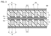
- FIG. 3 is a cross-sectional view of the printed wiring board 200.
- the printed wiring board 200 includes a base film 50, a conductive pattern 61 and a conductive pattern 62, and a coverlay film 100.
- the base film 50 has a third main surface 50a and a fourth main surface 50b.
- the third main surface 50a and the fourth main surface 50b are end faces of the base film 50 in the thickness direction.
- the fourth main surface 50b is the opposite surface to the third main surface 50a.
- the base film 50 is made of a flexible electrically insulating material.
- the base film 50 is made of polyimide, for example.
- the base film 50 may be formed of a liquid crystal polymer. However, the constituent material of the base film 50 is not limited to this.
- the conductive pattern 61 and the conductive pattern 62 are arranged on the third main surface 50a and the fourth main surface 50b, respectively.
- the conductive pattern 61 and the conductive pattern 62 are formed by, for example, a semi-additive method. More specifically, each of the conductive pattern 61 and the conductive pattern 62 includes a seed layer 63, an electroless plating layer 64, and an electrolytic plating layer 65. However, the conductive pattern 61 and the conductive pattern 62 may be formed by a subtractive method.
- the thickness of the conductive pattern 61 and the thickness of the conductive pattern 62 are defined as a thickness T4 and a thickness T5, respectively.
- the thickness T4 and the thickness T5 are, for example, 10 ⁇ m or more and 60 ⁇ m or less.
- the distance between two adjacent conductive patterns 61 is defined as a distance DIS1.
- the distance between two adjacent conductive patterns 62 is defined as a distance DIS2.
- the distance DIS1 and the distance DIS2 are, for example, 5 ⁇ m or more and 50 ⁇ m or less.
- the seed layer 63 is arranged on the main surfaces (third main surface 50a, fourth main surface 50b) of the base film 50.
- the seed layer 63 is, for example, a sputter layer (a layer formed by sputtering).
- the seed layer 63 is arranged, for example, on a nickel-chromium alloy layer disposed on the main surface (third main surface 50a, fourth main surface 50b) of the base film 50 and on a nickel-chromium alloy layer. It is made up of a layer of copper.
- the electroless plating layer 64 is arranged on the seed layer 63.
- the electroless plating layer 64 is a layer formed by electroless plating.
- the electroless plating layer 64 is made of copper, for example.
- Electrolytic plating layer 65 is arranged on electroless plating layer 64.
- the electroplated layer 65 is a layer formed by electrolytic plating.
- the electrolytic plating layer 65 is made of copper, for example.
- the coverlay film 100 is arranged on the third main surface 50a so that the adhesive layer 20 covers the conductive pattern 61.
- the coverlay film 100 is also arranged on the fourth main surface 50b so that the adhesive layer 20 covers the conductive pattern 62.
- the adhesive constituting the adhesive layer 20 has been cured, and the protective film 40 has been peeled off from the insulating film 10.
- the conductive pattern 61 and the conductive pattern 62 are arranged on the third main surface 50a and the fourth main surface 50b, respectively. It is not necessary to have either one of the patterns 62. Note that when the printed wiring board 200 does not have the conductive pattern 61, the coverlay film 100 is not attached on the third main surface 50a, and when the printed wiring board 200 does not have the conductive pattern 62, In this case, the coverlay film 100 is not attached on the fourth main surface 50b.
- FIG. 4 is a manufacturing process diagram of the printed wiring board 200.
- the method for manufacturing printed wiring board 200 includes a preparation step S4, a separator peeling step S5, a coverlay film placement step S6, and a protective film peeling step S7.
- the separator peeling step S5 is performed after the preparation step S4.
- the coverlay film arrangement step S6 is performed after the separator peeling step S5.
- the protective film peeling step S7 is performed after the coverlay film placement step S6.
- the base film 50 and the coverlay film 100 are prepared.
- a conductive pattern 61 and a conductive pattern 62 are arranged on the third main surface 50a and the fourth main surface 50b, respectively.
- the separator 30 is peeled off from the adhesive layer 20 in the coverlay film 100 prepared in the preparation step S4.
- the coverlay film 100 is arranged on the third main surface 50a so that the adhesive layer 20 covers the conductive pattern 61, and the coverlay film 100 is arranged so that the adhesive layer 20 covers the conductive pattern 62.
- the coverlay film 100 is placed on the fourth main surface 50b.
- the coverlay film 100 is arranged on the third main surface 50a so that the adhesive layer 20 covers the conductive pattern 61, and the adhesive layer 20 covers the conductive pattern 61.
- a coverlay film 100 is placed on the fourth main surface 50b so as to cover the fourth main surface 50b.
- the base film 50 to which the coverlay film 100 is attached is heated and pressurized. As a result, the adhesive constituting the adhesive layer 20 is cured, and the coverlay film 100 is attached to the third main surface 50a and the fourth main surface 50b.
- the protective film peeling step S7 the protective film 40 is peeled off from the insulating film 10.
- printed wiring board 200 having the structure shown in FIG. 3 is manufactured. Note that if the protective film 40 is peeled off from the insulating film 10 after the separator arrangement step S3 is performed, the protective film peeling step S7 may not be performed.
- the thickness T1 is large, the thickness of the printed wiring board 200 also becomes large, and the printed wiring board 200 cannot be made thinner.
- the thickness T2 is small and the distance DIS1 (distance DIS2) becomes small, the adhesive layer 20 cannot fill in the spaces between adjacent conductive patterns 61 (conductive patterns 62).
- the thickness T1 is small (specifically, 2 ⁇ m or more and 15 ⁇ m or less), and the thickness T2 is large (specifically, 10 ⁇ m or more and 50 ⁇ m or less). Therefore, according to the coverlay film 100, it is possible to reduce the thickness of the printed wiring board 200 while improving the embeddability of the adhesive layer 20 between adjacent conductive patterns 61 (conductive patterns 62). be.
- the rigidity of the coverlay film 100 decreases, which may make handling difficult.
- the rigidity of the coverlay film 100 is increased, so that the handling properties of the coverlay film 100 can be improved. .
- the protective film 40 on the second main surface 10b, it is possible to suppress the occurrence of damage to the insulating film 10 (for example, surface scratches, dents, tears, burrs, etc.).
- the coverlay film 100 may fall down when the adhesive layer 20 is dried with hot air. However, since the coverlay film 100 has the protective film 40 disposed on the second main surface 10b, it is suppressed from falling down when the adhesive layer 20 is dried.
- the thickness T1 is small (more specifically, 2 ⁇ m or more and 15 ⁇ m or less), and the thickness T2 is large (more specifically, 10 ⁇ m or more and 50 ⁇ m or less). Therefore, according to the printed wiring board 200, it is possible to reduce the thickness of the printed wiring board 200 while improving the embeddability of the adhesive layer 20 between adjacent conductive patterns 61 (conductive patterns 62). .
Landscapes
- Engineering & Computer Science (AREA)
- Microelectronics & Electronic Packaging (AREA)
- Manufacturing & Machinery (AREA)
- Non-Metallic Protective Coatings For Printed Circuits (AREA)
Priority Applications (3)
| Application Number | Priority Date | Filing Date | Title |
|---|---|---|---|
| JP2024512256A JPWO2023190004A1 (https=) | 2022-03-31 | 2023-03-23 | |
| US18/850,596 US20250220822A1 (en) | 2022-03-31 | 2023-03-23 | Coverlay film, printed wiring board, method for manufacturing coverlay film, and method for manufacturing printed wiring board |
| CN202380025562.9A CN118830336A (zh) | 2022-03-31 | 2023-03-23 | 覆盖层用膜、印刷布线板、覆盖层用膜的制造方法及印刷布线板的制造方法 |
Applications Claiming Priority (2)
| Application Number | Priority Date | Filing Date | Title |
|---|---|---|---|
| JP2022059505 | 2022-03-31 | ||
| JP2022-059505 | 2022-03-31 |
Publications (1)
| Publication Number | Publication Date |
|---|---|
| WO2023190004A1 true WO2023190004A1 (ja) | 2023-10-05 |
Family
ID=88201989
Family Applications (1)
| Application Number | Title | Priority Date | Filing Date |
|---|---|---|---|
| PCT/JP2023/011435 Ceased WO2023190004A1 (ja) | 2022-03-31 | 2023-03-23 | カバーレイ用フィルム、プリント配線板、カバーレイ用フィルムの製造方法及びプリント配線板の製造方法 |
Country Status (5)
| Country | Link |
|---|---|
| US (1) | US20250220822A1 (https=) |
| JP (1) | JPWO2023190004A1 (https=) |
| CN (1) | CN118830336A (https=) |
| TW (1) | TW202402987A (https=) |
| WO (1) | WO2023190004A1 (https=) |
Citations (3)
| Publication number | Priority date | Publication date | Assignee | Title |
|---|---|---|---|---|
| WO2016063757A1 (ja) * | 2014-10-21 | 2016-04-28 | 住友電工プリントサーキット株式会社 | 樹脂フィルム、プリント配線板用カバーレイ、プリント配線板用基板及びプリント配線板 |
| JP2019116619A (ja) * | 2013-09-12 | 2019-07-18 | 住友電気工業株式会社 | プリント配線板用接着剤組成物、ボンディングフィルム、カバーレイ、銅張積層板及びプリント配線板 |
| WO2021131244A1 (ja) * | 2019-12-25 | 2021-07-01 | タツタ電線株式会社 | 電磁波シールドフィルム |
-
2023
- 2023-03-23 WO PCT/JP2023/011435 patent/WO2023190004A1/ja not_active Ceased
- 2023-03-23 US US18/850,596 patent/US20250220822A1/en active Pending
- 2023-03-23 CN CN202380025562.9A patent/CN118830336A/zh active Pending
- 2023-03-23 JP JP2024512256A patent/JPWO2023190004A1/ja active Pending
- 2023-03-28 TW TW112111619A patent/TW202402987A/zh unknown
Patent Citations (3)
| Publication number | Priority date | Publication date | Assignee | Title |
|---|---|---|---|---|
| JP2019116619A (ja) * | 2013-09-12 | 2019-07-18 | 住友電気工業株式会社 | プリント配線板用接着剤組成物、ボンディングフィルム、カバーレイ、銅張積層板及びプリント配線板 |
| WO2016063757A1 (ja) * | 2014-10-21 | 2016-04-28 | 住友電工プリントサーキット株式会社 | 樹脂フィルム、プリント配線板用カバーレイ、プリント配線板用基板及びプリント配線板 |
| WO2021131244A1 (ja) * | 2019-12-25 | 2021-07-01 | タツタ電線株式会社 | 電磁波シールドフィルム |
Also Published As
| Publication number | Publication date |
|---|---|
| US20250220822A1 (en) | 2025-07-03 |
| JPWO2023190004A1 (https=) | 2023-10-05 |
| CN118830336A (zh) | 2024-10-22 |
| TW202402987A (zh) | 2024-01-16 |
Similar Documents
| Publication | Publication Date | Title |
|---|---|---|
| TWI233771B (en) | Flexible rigid printed circuit board and method of fabricating the board | |
| US7293353B2 (en) | Method of fabricating rigid flexible printed circuit board | |
| US20170118833A1 (en) | Multilayer rigid flexible printed circuit board and method for manufacturing the same | |
| JPH04152693A (ja) | 多層配線基板および多層配線基板の製造方法 | |
| CN101296562A (zh) | 铜箔基板以及利用该铜箔基板制作软性印刷电路板的方法 | |
| JP5955102B2 (ja) | 配線基板およびその製造方法 | |
| US20100018638A1 (en) | Method for manufacturing flexible printed circuit board | |
| US7931818B2 (en) | Process of embedded circuit structure | |
| US8067696B2 (en) | Printed circuit board and method for manufacturing same | |
| TW201813458A (zh) | 鏤空柔性電路板及製作方法 | |
| JP2013541856A (ja) | 新規なプリント回路基板及びその製造方法 | |
| WO2023190004A1 (ja) | カバーレイ用フィルム、プリント配線板、カバーレイ用フィルムの製造方法及びプリント配線板の製造方法 | |
| TWI519225B (zh) | 多層軟性線路結構的製作方法 | |
| TWI655095B (zh) | Nano metal substrate for FPC and COF materials | |
| JPH0992980A (ja) | フレキシブル部分を有する多層プリント配線板及びその製造方法 | |
| US6713682B1 (en) | Through hole conduction structure of flexible multilayer circuit board and forming method thereof | |
| US20190335593A1 (en) | Method of manufacturing the printed circuit board | |
| JP5057339B2 (ja) | 配線基板の製造方法 | |
| JP3749201B2 (ja) | プリント配線板の製造方法 | |
| JP2007221068A (ja) | フラッシュプリント配線板およびその製造方法ならびにフラッシュプリント配線板からなる多層プリント配線板。 | |
| JPH10178241A (ja) | プリント配線板及びその製造方法 | |
| JP5549853B2 (ja) | マルチワイヤ配線板及びその製造方法 | |
| TWI519224B (zh) | 多層軟性線路結構的製作方法 | |
| JPWO2023190004A5 (https=) | ||
| KR20140137628A (ko) | 연성회로기판의 구조 |
Legal Events
| Date | Code | Title | Description |
|---|---|---|---|
| 121 | Ep: the epo has been informed by wipo that ep was designated in this application |
Ref document number: 23780015 Country of ref document: EP Kind code of ref document: A1 |
|
| ENP | Entry into the national phase |
Ref document number: 2024512256 Country of ref document: JP Kind code of ref document: A |
|
| WWE | Wipo information: entry into national phase |
Ref document number: 202380025562.9 Country of ref document: CN |
|
| WWE | Wipo information: entry into national phase |
Ref document number: 18850596 Country of ref document: US |
|
| NENP | Non-entry into the national phase |
Ref country code: DE |
|
| 122 | Ep: pct application non-entry in european phase |
Ref document number: 23780015 Country of ref document: EP Kind code of ref document: A1 |
|
| WWP | Wipo information: published in national office |
Ref document number: 18850596 Country of ref document: US |