WO2023189954A1 - 試料保持具 - Google Patents
試料保持具 Download PDFInfo
- Publication number
- WO2023189954A1 WO2023189954A1 PCT/JP2023/011273 JP2023011273W WO2023189954A1 WO 2023189954 A1 WO2023189954 A1 WO 2023189954A1 JP 2023011273 W JP2023011273 W JP 2023011273W WO 2023189954 A1 WO2023189954 A1 WO 2023189954A1
- Authority
- WO
- WIPO (PCT)
- Prior art keywords
- sample holder
- base plate
- cylindrical member
- ceramic substrate
- holder according
- Prior art date
- Legal status (The legal status is an assumption and is not a legal conclusion. Google has not performed a legal analysis and makes no representation as to the accuracy of the status listed.)
- Ceased
Links
Images






Classifications
-
- H—ELECTRICITY
- H10—SEMICONDUCTOR DEVICES; ELECTRIC SOLID-STATE DEVICES NOT OTHERWISE PROVIDED FOR
- H10P—GENERIC PROCESSES OR APPARATUS FOR THE MANUFACTURE OR TREATMENT OF DEVICES COVERED BY CLASS H10
- H10P72/00—Handling or holding of wafers, substrates or devices during manufacture or treatment thereof
- H10P72/70—Handling or holding of wafers, substrates or devices during manufacture or treatment thereof for supporting or gripping
- H10P72/76—Handling or holding of wafers, substrates or devices during manufacture or treatment thereof for supporting or gripping using mechanical means, e.g. clamps or pinches
- H10P72/7604—Handling or holding of wafers, substrates or devices during manufacture or treatment thereof for supporting or gripping using mechanical means, e.g. clamps or pinches the wafers being placed on a susceptor, stage or support
- H10P72/7616—Handling or holding of wafers, substrates or devices during manufacture or treatment thereof for supporting or gripping using mechanical means, e.g. clamps or pinches the wafers being placed on a susceptor, stage or support characterised by a coating, a hardness or a material
-
- H—ELECTRICITY
- H01—ELECTRIC ELEMENTS
- H01J—ELECTRIC DISCHARGE TUBES OR DISCHARGE LAMPS
- H01J37/00—Discharge tubes with provision for introducing objects or material to be exposed to the discharge, e.g. for the purpose of examination or processing thereof
- H01J37/32—Gas-filled discharge tubes
- H01J37/32431—Constructional details of the reactor
- H01J37/32715—Workpiece holder
-
- H—ELECTRICITY
- H10—SEMICONDUCTOR DEVICES; ELECTRIC SOLID-STATE DEVICES NOT OTHERWISE PROVIDED FOR
- H10P—GENERIC PROCESSES OR APPARATUS FOR THE MANUFACTURE OR TREATMENT OF DEVICES COVERED BY CLASS H10
- H10P72/00—Handling or holding of wafers, substrates or devices during manufacture or treatment thereof
- H10P72/04—Apparatus for manufacture or treatment
- H10P72/0431—Apparatus for thermal treatment
- H10P72/0432—Apparatus for thermal treatment mainly by conduction
-
- H—ELECTRICITY
- H10—SEMICONDUCTOR DEVICES; ELECTRIC SOLID-STATE DEVICES NOT OTHERWISE PROVIDED FOR
- H10P—GENERIC PROCESSES OR APPARATUS FOR THE MANUFACTURE OR TREATMENT OF DEVICES COVERED BY CLASS H10
- H10P72/00—Handling or holding of wafers, substrates or devices during manufacture or treatment thereof
- H10P72/04—Apparatus for manufacture or treatment
- H10P72/0431—Apparatus for thermal treatment
- H10P72/0434—Apparatus for thermal treatment mainly by convection
-
- H—ELECTRICITY
- H10—SEMICONDUCTOR DEVICES; ELECTRIC SOLID-STATE DEVICES NOT OTHERWISE PROVIDED FOR
- H10P—GENERIC PROCESSES OR APPARATUS FOR THE MANUFACTURE OR TREATMENT OF DEVICES COVERED BY CLASS H10
- H10P72/00—Handling or holding of wafers, substrates or devices during manufacture or treatment thereof
- H10P72/04—Apparatus for manufacture or treatment
- H10P72/0441—Apparatus for sealing, encapsulating, glassing, decapsulating or the like
-
- H—ELECTRICITY
- H10—SEMICONDUCTOR DEVICES; ELECTRIC SOLID-STATE DEVICES NOT OTHERWISE PROVIDED FOR
- H10P—GENERIC PROCESSES OR APPARATUS FOR THE MANUFACTURE OR TREATMENT OF DEVICES COVERED BY CLASS H10
- H10P72/00—Handling or holding of wafers, substrates or devices during manufacture or treatment thereof
- H10P72/70—Handling or holding of wafers, substrates or devices during manufacture or treatment thereof for supporting or gripping
-
- H—ELECTRICITY
- H10—SEMICONDUCTOR DEVICES; ELECTRIC SOLID-STATE DEVICES NOT OTHERWISE PROVIDED FOR
- H10P—GENERIC PROCESSES OR APPARATUS FOR THE MANUFACTURE OR TREATMENT OF DEVICES COVERED BY CLASS H10
- H10P72/00—Handling or holding of wafers, substrates or devices during manufacture or treatment thereof
- H10P72/70—Handling or holding of wafers, substrates or devices during manufacture or treatment thereof for supporting or gripping
- H10P72/72—Handling or holding of wafers, substrates or devices during manufacture or treatment thereof for supporting or gripping using electrostatic chucks
-
- H—ELECTRICITY
- H10—SEMICONDUCTOR DEVICES; ELECTRIC SOLID-STATE DEVICES NOT OTHERWISE PROVIDED FOR
- H10P—GENERIC PROCESSES OR APPARATUS FOR THE MANUFACTURE OR TREATMENT OF DEVICES COVERED BY CLASS H10
- H10P72/00—Handling or holding of wafers, substrates or devices during manufacture or treatment thereof
- H10P72/70—Handling or holding of wafers, substrates or devices during manufacture or treatment thereof for supporting or gripping
- H10P72/76—Handling or holding of wafers, substrates or devices during manufacture or treatment thereof for supporting or gripping using mechanical means, e.g. clamps or pinches
- H10P72/7604—Handling or holding of wafers, substrates or devices during manufacture or treatment thereof for supporting or gripping using mechanical means, e.g. clamps or pinches the wafers being placed on a susceptor, stage or support
- H10P72/7624—Handling or holding of wafers, substrates or devices during manufacture or treatment thereof for supporting or gripping using mechanical means, e.g. clamps or pinches the wafers being placed on a susceptor, stage or support characterised by the mechanical construction of the susceptor, stage or support
Definitions
- the disclosed embodiments relate to a sample holder.
- a sample holder includes a ceramic substrate, a base plate, and a cylindrical member.
- the ceramic substrate has a first surface that is a sample holding surface and a second surface located opposite to the first surface.
- the base plate is located on the second surface of the ceramic substrate, and extends through a third surface that is opposite to the second surface, a fourth surface that is opposite to the third surface, and the third and fourth surfaces. It has a through hole.
- the cylindrical member is located in the through hole and is joined to the second surface.
- a sample holder includes a sealing member between the inner peripheral surface of the through hole and the outer peripheral surface of the cylindrical member.
- FIG. 1 is a schematic cross-sectional view showing a configuration example of a semiconductor manufacturing apparatus using the sample holder according to the first embodiment.
- FIG. 2 is a schematic cross-sectional view showing a configuration example of the sample holder according to the first embodiment.
- FIG. 3 is a schematic cross-sectional view showing a configuration example of a sample holder according to the second embodiment.
- FIG. 4 is a schematic enlarged view of one end of the cylindrical member.
- FIG. 5 is a schematic cross-sectional view showing a configuration example of a sample holder according to the third embodiment.
- FIG. 6 is a schematic cross-sectional view showing an example of the structure of the groove portion.
- FIG. 7 is a schematic cross-sectional view showing an example of the structure of the groove.
- FIG. 1 is a schematic cross-sectional view showing a configuration example of a semiconductor manufacturing apparatus using the sample holder according to the first embodiment.
- FIG. 2 is a schematic cross-sectional view showing a configuration example of the sample
- FIG. 8 is a schematic cross-sectional view showing an example of the structure of the groove.
- FIG. 9 is a schematic cross-sectional view showing an example of the structure of the groove portion.
- FIG. 10 is a schematic cross-sectional view showing a configuration example of a sample holder according to the fourth embodiment.
- FIG. 11 is a schematic cross-sectional view showing a configuration example of a sample holder according to the fifth embodiment.
- FIG. 12 is a schematic cross-sectional view showing a configuration example of a sample holder according to the sixth embodiment.
- FIG. 13 is a schematic cross-sectional view showing a configuration example of a sample holder according to the seventh embodiment.
- FIG. 14 is a schematic cross-sectional view showing a configuration example of a sample holder according to the eighth embodiment.
- FIG. 10 is a schematic cross-sectional view showing a configuration example of a sample holder according to the fourth embodiment.
- FIG. 11 is a schematic cross-sectional view showing a configuration example of
- FIG. 15 is a schematic cross-sectional view showing a configuration example of a sample holder according to the eighth embodiment.
- FIG. 16 is a schematic cross-sectional view showing a configuration example of a sample holder according to the ninth embodiment.
- FIG. 17 is a schematic cross-sectional view showing a configuration example of a sample holder according to the tenth embodiment.
- FIG. 18 is a schematic cross-sectional view showing a configuration example of a sample holder according to the eleventh embodiment.
- FIG. 19 is a schematic cross-sectional view showing a configuration example of a sample holder according to the twelfth embodiment.
- sample holder according to the present disclosure is used in a semiconductor manufacturing device that processes semiconductor wafers will be described below, but the sample holder according to the present disclosure may also be used for holding samples other than semiconductor wafers. It's okay.
- FIG. 1 is a schematic cross-sectional view showing a configuration example of a semiconductor manufacturing apparatus using the sample holder according to the first embodiment.
- FIG. 1 mainly shows the components necessary for explaining the sample holder among the components included in the semiconductor manufacturing apparatus, and other components are omitted as appropriate.
- the semiconductor manufacturing device may be a plasma processing device that processes semiconductor wafers using plasma.
- the semiconductor manufacturing apparatus may include a shower head that functions as an electrode for plasma generation.
- the semiconductor manufacturing apparatus 100 includes a sample holder 1, a processing container 2, a first sealing member 3, and an exhaust mechanism 4.
- the sample holder 1 places a sample to be processed (here, a semiconductor wafer). The specific configuration of the sample holder 1 will be described later.
- the processing container 2 accommodates the sample holder 1.
- An opening 21 is located at the bottom of the processing container 2 .
- a terminal 16, which will be described later, is inserted into the opening 21. In other words, the terminal 16 is drawn out of the processing container 2 through the opening 21.
- the first sealing member 3 is, for example, a rubber O-ring.
- the first sealing member 3 is located so as to surround the opening 21 of the processing container 2 .
- the first sealing member 3 is located between the lower surface of the sample holder 1 and the bottom surface of the processing container 2, and is crushed between the sample holder 1 and the processing container 2 from above. Seal the gap between the Thereby, the inside of the processing container 2 is sealed.
- the exhaust mechanism 4 is connected to an exhaust port (not shown) of the processing container 2 via an exhaust pipe 41.
- the exhaust mechanism 4 includes a vacuum pump, a pressure control valve, and the like, and exhausts the inside of the processing container 2 via an exhaust pipe 41. As a result, the pressure inside the processing container 2 is reduced.
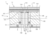
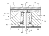
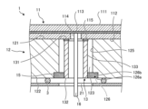
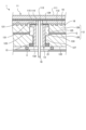
- FIG. 2 is a schematic cross-sectional view showing a configuration example of the sample holder 1 according to the first embodiment.
- the sample holder 1 includes a ceramic substrate 11, a base plate 12, a cylindrical member 13, a plurality of fixing parts 14, a second sealing member 15, and a terminal 16.
- the ceramic substrate 11 has, for example, a disk shape.
- the first surface 111 which is one main surface (here, the top surface) of the ceramic substrate 11, is a holding surface for a semiconductor wafer.
- the ceramic substrate 11 is mainly made of, for example, aluminum oxide (Al 2 O 3 ), aluminum nitride (AlN), yttria (Y 2 O 3 ), cordierite, silicon carbide (SiC), or silicon nitride (Si 3 N 4 ). It may be included as an ingredient.
- the ceramic substrate 11 is obtained, for example, by laminating and firing a plurality of green sheets.
- a heating resistor 113 is located inside the ceramic substrate 11.
- the heating resistor 113 is a member that generates heat when a current flows therethrough.
- the heating resistor 113 is provided to heat the semiconductor wafer held on the first surface 111.
- the heating resistor 113 may have a linear pattern (meander pattern) having a plurality of folded portions.
- the heating resistor 113 includes, for example, a metal material.
- the metal material constituting the heating resistor 113 include tungsten, molybdenum, rhenium, alloys thereof, and platinum.
- the heating resistor 113 may contain a glass component such as an oxide such as silicon dioxide, for example.
- a conductive member other than the heating resistor 113 may be located inside the ceramic substrate 11.
- an electrode for electrostatic adsorption or a high-frequency electrode to which high-frequency power for plasma generation is applied may be located inside the ceramic substrate 11 .
- the metal material constituting the electrostatic adsorption electrode and the high-frequency electrode include tungsten, molybdenum, rhenium, alloys thereof, and platinum.
- a recess 114 that reaches the heating resistor 113 is located on the second surface 112 (lower surface here) that is the opposite surface to the first surface 111 of the ceramic substrate 11 .
- the base plate 12 has, for example, a disk shape with a larger diameter than the ceramic substrate 11.
- Base plate 12 is located on second surface 112 of ceramic substrate 11 .
- the base plate 12 has a third surface 121 (here, the upper surface) that is opposite to the second surface 112, and a fourth surface 122 (here, the lower surface) located opposite to the third surface 121. and has.
- the base plate 12 has a through hole 123 that passes through the third surface 121 and the fourth surface 122.
- the heating resistor 113 built into the ceramic substrate 11 is exposed to the outside through the opening 21 of the processing chamber 2 , the through hole 123 of the base plate 12 , and the recess 114 of the ceramic substrate 11 .
- the base plate 12 may be made of metal, for example.
- the metal base plate 12 functions as a cooling member for cooling the ceramic substrate 11 heated by the heating resistor 113.
- the base plate 12 as a cooling member may have an internal flow path through which a cooling medium such as cooling water or cooling gas flows. Further, the metal base plate 12 may be used as a high frequency electrode to which high frequency power for plasma generation is applied.
- the cylindrical member 13 has, for example, a cylindrical shape.
- the cylindrical member 13 is inserted into the through hole 123 of the base plate 12. In other words, the cylindrical member 13 is located in the through hole 123.
- a fifth surface 131 which is one of both end surfaces (here, the upper end surface) of the cylindrical member 13, is bonded to the second surface 112 of the ceramic substrate 11 via a bonding member 115.
- the joining member 115 is, for example, glass or brazing material.
- the outer diameter of the cylindrical member 13 is smaller than the inner diameter of the through hole 123 of the processing container 2. That is, the inner circumferential surface 125 of the through hole 123 and the outer circumferential surface 133 of the cylindrical member 13 are apart, and there is a gap (space) between the outer circumferential surface 133 of the cylindrical member 13 and the inner circumferential surface 125 of the through hole 123. ) is located.
- the sixth surface 132 which is the other surface (here, the lower end surface) of both end surfaces of the cylindrical member 13, may protrude from the opening 21 of the processing container 2 to the outside of the processing container 2.
- a terminal 16 is inserted into the cylindrical member 13.
- the terminal 16 is connected to the heating resistor 113 via the cylindrical member 13 and the recess 114 of the ceramic substrate 11 .
- the fixing part 14 mechanically joins the ceramic substrate 11 and the base plate 12 by sandwiching the ceramic substrate 11 and the base plate 12.
- the fixed part 14 includes a support member 141, a claw member 142, and a fastening member 143.
- the strut member 141 is a member extending in the vertical direction.
- the strut member 141 is inserted into an insertion hole 124 provided in the base plate 12 and extends above the base plate 12 through the insertion hole 124.
- the claw member 142 extends horizontally from the tip of the support member 141 and comes into contact with the outer circumference of the first surface 111 of the ceramic substrate 11 .
- the fastening member 143 is, for example, a nut.
- the fastening member 143 is provided at the base end of the column member 141 and abuts against a step provided inside the insertion hole 124 .
- the fixing portion 14 fastens the fastening member 143 to the support member 141, thereby moving the support member 141 and the claw member 142 downward. Thereby, the ceramic substrate 11 and the base plate 12 are pressed against each other, so that the ceramic substrate 11 and the base plate 12 are joined.
- the configuration of the fixing portion 14 shown in FIG. 1 is an example, and any configuration may be used as long as it mechanically joins the ceramic substrate 11 and the base plate 12.
- the ceramic substrate 11 and base plate 12 are mechanically bonded, there is no need to bond the ceramic substrate 11 and base plate 12 with an adhesive. Therefore, it becomes easy to use the sample holder 1 in a high temperature environment.
- the sealing performance between the ceramic substrate 11 and the base plate 12 is secured compared to the case where the ceramic substrate 11 and the base plate 12 are bonded with adhesive. It becomes difficult to do so. Therefore, there is a risk that vacuum leakage will occur in the gap between the ceramic substrate 11 and the base plate 12, making it difficult to maintain the reduced pressure state of the processing container 2.
- the gap between the inner peripheral surface 125 of the through hole 123 and the outer peripheral surface 133 of the cylindrical member 13 is sealed with the second sealing member 15.
- the second sealing member 15 is, for example, a rubber-like member such as silicone resin.
- the second sealing member 15 is located between the inner peripheral surface 125 of the through hole 123 and the outer peripheral surface 133 of the cylindrical member 13 and seals the gap between the through hole 123 and the cylindrical member 13 .
- the gap between the inner circumferential surface 125 of the through hole 123 communicating with the gap between the ceramic substrate 11 and the base plate 12 and the outer circumferential surface 133 of the cylindrical member 13 with the second sealing member 15 Even if the sealing performance between the ceramic substrate 11 and the base plate 12 is not sufficiently ensured, the occurrence of vacuum leakage can be reduced.
- the gap between the inner circumferential surface 125 of the through hole 123 where the second sealing member 15 is located and the outer circumferential surface 133 of the cylindrical member 13 is larger than the gap between the ceramic substrate 11 and the base plate 12, which is a heat source. 11, it is less susceptible to the effects of heat from the ceramic substrate 11. Therefore, according to the sample holder 1 according to the embodiment, it is easy to ensure sealing performance in a high-temperature environment.
- the second sealing member 15 is located closer to the fourth surface 122 of the base plate 12 than the center C in the thickness direction of the base plate 12. In other words, the second sealing member 15 is located between the center C of the base plate 12 in the thickness direction and the fourth surface 122 of the base plate 12 . With this configuration, it is possible to make the ceramic substrate 11 less susceptible to heat from the ceramic substrate 11.
- the space between the inner circumferential surface 125 of the through hole 123 and the outer circumferential surface 133 of the cylindrical member 13 functions as a heat insulating layer.
- the thermal influence on the second sealing member 15 can be further reduced.
- the second sealing member 15 only needs to be located between the center C of the base plate 12 in the thickness direction and the fourth surface 122 of the base plate 12. That is, a part of the second sealing member 15 may protrude onto the fourth surface 122 of the base plate 12 or may be located between the center C of the base plate 12 in the thickness direction and the third surface 121 of the base plate 12. You can leave it there. Further, the second sealing member 15 may be provided flush with the fourth surface 122 of the base plate 12.
- the thermal expansion coefficient of the cylindrical member 13 may be smaller than that of the ceramic substrate 11.
- thermal expansion and contraction in the longitudinal direction of the cylindrical member 13 thickness direction of the ceramic substrate 11 and the base plate 12
- the stress applied to the joint surface between the cylindrical member 13 and the second sealing member 15 can be reduced. Therefore, reliability in a high temperature environment can be further improved.
- mullite can be used as a material for the cylindrical member 13 having a coefficient of thermal expansion smaller than that of the ceramic substrate 11.
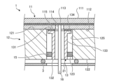
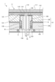
- FIG. 3 is a schematic cross-sectional view showing a configuration example of the sample holder 1 according to the second embodiment.
- the area of the fifth surface 131 which is the joint surface with the second surface 112 of the ceramic substrate 11, may be larger than the area of the sixth surface 132, which is located opposite to the fifth surface 131.
- one end 134 located on the ceramic substrate 11 side may have a flange shape.
- the fifth surface 131 which is the upper surface of one end 134, has a larger area than the sixth surface 132, which is the lower surface of the other end.
- the bonding area between the ceramic substrate 11 and the cylindrical member 13 becomes large, so that it is possible to suitably reduce the occurrence of vacuum leakage from the gap between the ceramic substrate 11 and the cylindrical member 13. .
- an increase in the heat capacity of the cylindrical member 13 can be reduced. Thereby, the influence of heat on the second sealing member 15 due to heat conduction from the ceramic substrate 11 can be reduced.
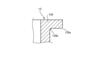
- FIG. 4 is a schematic enlarged view of one end portion 134 of the cylindrical member 13. As shown in FIG. 4, a corner 135a of one end 134 of the cylindrical member 13 may be curved in an R shape. Similarly, the corner 135b of the one end 134 of the cylindrical member 13 may be curved in an R shape.
- FIG. 4 shows an example in which both the corner 135a and the corner 135b are curved
- the one end 134 of the cylindrical member 13 has at least the corner 135a and the corner 135b curved. That's fine.
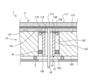
- FIG. 5 is a schematic cross-sectional view showing a configuration example of the sample holder 1 according to the third embodiment.
- the cylindrical member 13 may have a groove 136 on the fifth surface 131, which is the upper surface of the flange-like one end 134.
- the contact area between the fifth surface 131 and the joining member 115 becomes larger, so that the ceramic substrate 11 and the cylindrical member 13 can be joined more firmly.
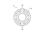
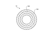
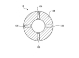
- FIGS. 6 to 9 are schematic cross-sectional views showing examples of the configuration of the groove portion 136. Specifically, FIGS. 6 to 9 show a plane cross section when one end 134 of the cylindrical member 13 is cut at a position above the bottom surface of the groove 136 and below the fifth surface 131 of the cylindrical member 13. The figure shows.
- the cylindrical member 13 may have a groove 136 extending in the circumferential direction.
- FIG. 6 shows an example in which the cylindrical member 13 has a plurality of grooves 136 arranged in the circumferential direction.
- FIG. 7 shows an example in which the cylindrical member 13 has an annular groove portion 136.
- the cylindrical member 13 may have a groove 136 extending in the radial direction.
- FIG. 8 shows an example in which the cylindrical member 13 has a groove 136 extending across the inner and outer peripheral edges of the cylindrical member 13.
- FIG. 9 shows an example in which the cylindrical member 13 has a groove portion 136 at one end and the other end having a length that does not reach the inner peripheral edge and the outer peripheral edge of the cylindrical member 13, respectively.
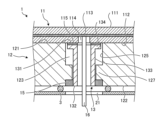
- FIG. 10 is a schematic cross-sectional view showing a configuration example of the sample holder 1 according to the fourth embodiment.
- the shape of the cylindrical member 13 in which the area of the fifth surface 131 is larger than the area of the sixth surface 132 is not limited to the shape shown in FIG. 3.
- the cylindrical member 13 may have a tapered shape that gradually becomes narrower from the fifth surface 131 toward the sixth surface 132. Even in such a configuration, since the bonding area between the ceramic substrate 11 and the cylindrical member 13 becomes large, it is possible to suitably reduce the occurrence of vacuum leakage from the gap between the ceramic substrate 11 and the cylindrical member 13. can. Further, by forming the cylindrical member 13 into a tapered shape, an increase in heat capacity of the cylindrical member 13 can be reduced compared to a case where the cylindrical member 13 is made uniformly thick. Thereby, the influence of heat on the second sealing member 15 due to heat conduction from the ceramic substrate 11 can be reduced.
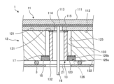
- FIG. 11 is a schematic cross-sectional view showing a configuration example of the sample holder 1 according to the fifth embodiment.
- the base plate 12 may have a counterbore 126 recessed in the thickness direction of the base plate 12 at the opening of the fourth surface 122 in the through hole 123.
- the counterbore portion 126 has a larger diameter than the through hole 123 of the base plate 12. Specifically, the counterbored portion 126 has a side surface 126a located further away from the outer circumferential surface 133 of the cylindrical member 13 than the inner circumferential surface 125 of the through hole 123 in the radial direction of the cylindrical member 13. Further, the counterbore portion 126 has a step surface 126b between the side surface 126a and the inner circumferential surface 125 of the through hole 123.
- the second sealing member 15 according to the fifth embodiment is located in this counterbore portion 126.
- the position, thickness, etc. of the second sealing member 15 can be easily controlled. Therefore, for example, it is possible to prevent the second sealing member 15 from coming too close to the ceramic substrate 11 or from having an insufficient thickness of the second sealing member 15. Furthermore, by positioning the base plate 12 between the second sealing member 15 and the ceramic substrate 11, the base plate 12 can reduce the radiant heat transmitted from the ceramic substrate 11 to the second sealing member 15. Therefore, reliability in use in high-temperature environments can be improved.
- FIG. 12 is a schematic cross-sectional view showing a configuration example of the sample holder 1 according to the sixth embodiment.
- the base plate 12 is disposed in the middle of the through hole 123 from the inner peripheral surface 125 of the through hole 123 toward the inside of the through hole 123, that is, toward the outer peripheral surface 133 of the cylindrical member 13. It may have a convex portion 127 (corresponding to an example of a first convex portion) that protrudes.
- the inner peripheral surface of the convex portion 127 has a smaller diameter than the inner peripheral surface 125 of the through hole 123 and a larger diameter than the outer peripheral surface 133 of the cylindrical member 13 .
- the lower side of the convex portion 127 performs the same function as the counterbore portion 126 (see FIG. 11) described above. That is, by positioning the second sealing member 15 below the convex portion 127, it becomes easier to control the position, thickness, etc. of the second sealing member 15. Further, by positioning the convex portion 127 between the second sealing member 15 and the ceramic substrate 11, the convex portion 127 can reduce the radiant heat transmitted from the ceramic substrate 11 to the second sealing member 15.
- the base plate 12 having the protrusion 127 can secure a larger heat-insulating space above the protrusion 127 than the base plate 12 having the counterbore 126. Thereby, the thermal influence on the second sealing member 15 can be reduced.
- FIG. 13 is a schematic cross-sectional view showing a configuration example of the sample holder 1 according to the seventh embodiment.
- the cylindrical member 13 has a through-hole in the base plate 12 extending from the outer circumferential surface 133 of the cylindrical member 13 toward the outside of the cylindrical member 13 at a midpoint in the thickness direction of the base plate 12. It may have a convex portion 137 (corresponding to an example of a second convex portion) that protrudes toward the inner circumferential surface 125 of 123 .
- the outer peripheral surface of the convex portion 137 has a larger diameter than the outer peripheral surface 133 of the cylindrical member 13 and has a smaller diameter than the inner peripheral surface 125 of the through hole 123 of the base plate 12.
- the lower side of the convex portion 137 performs the same function as the counterbore portion 126 described above (see FIG. 11). That is, by positioning the second sealing member 15 below the convex portion 137, it becomes easier to control the position, thickness, etc. of the second sealing member 15. Further, by positioning the convex portion 137 between the second sealing member 15 and the ceramic substrate 11, the convex portion 137 can reduce the radiant heat transmitted from the ceramic substrate 11 to the second sealing member 15. Further, by forming a heat insulating space above the convex portion 137, the influence of heat on the second sealing member 15 can be reduced.
- sample holder 1 may be configured to include a cylindrical member 13 (see FIG. 13) having a convex portion 137 and a base plate 12 (see FIG. 11) having a counterbore portion 126. Further, the sample holder 1 may include a cylindrical member 13 (see FIG. 13) having a convex portion 137 and a base plate 12 (see FIG. 12) having a convex portion 127.
- FIGS. 14 and 15 are schematic cross-sectional views showing a configuration example of the sample holder 1 according to the eighth embodiment.
- the sample holder 1 is located between the cylindrical member 13 and the base plate 12. Specifically, it may include an annular member 17 that fits into the gap between the cylindrical member 13 and the base plate 12.
- the annular member 17 may be made of metal, for example.
- FIG. 14 shows an example where the annular member 17 is located in the gap between the outer circumferential surface 133 of the tapered cylindrical member 13 and the inner circumferential surface 125 of the through hole 123. In this case, the annular member 17 is positioned by coming into contact with the outer peripheral surface 133 of the cylindrical member 13.
- FIG. 15 shows an example in which the annular member 17 is located on the stepped surface 126b of the counterbore portion 126 provided on the base plate 12. In this case, the annular member 17 is positioned by coming into contact with the stepped surface 126b.
- the inner diameter of the annular member 17 is larger than the outer peripheral surface 133 of the cylindrical member 13 and smaller than the inner peripheral surface 125 of the through hole 123. Further, the outer diameter of the annular member 17 is larger than the inner circumferential surface 125 of the through hole 123 and smaller than the side surface 126a of the counterbored portion 126.
- the second sealing member 15 is located in a region surrounded by the base plate 12, the cylindrical member 13, and the annular member 17.
- the second sealing can be achieved. It becomes easier to control the position, thickness, etc. of the member 15. Furthermore, the annular member 17 can reduce the radiant heat transmitted from the ceramic substrate 11 to the second sealing member 15 .
- FIG. 16 is a schematic cross-sectional view showing a configuration example of the sample holder 1 according to the ninth embodiment.
- the base plate 12 may include a cooling member 128, a heat-resistant member 129, and an adhesive G.
- the base plate 12 including the cooling member 128, the heat-resistant member 129, and the adhesive G has a disk shape with a larger diameter than the ceramic substrate 11 as a whole.
- the cooling member 128 has a fourth surface 122.
- Cooling member 128 may be made of metal, for example.
- the metal material forming the cooling member 128, for example an aluminum matrix composite material such as aluminum, stainless steel, titanium, or AlSiC can be used.
- the metal cooling member 128 can cool the ceramic substrate 11 heated by the heating resistor 113.
- the cooling member 128 may have an internal flow path through which a cooling medium such as cooling water or cooling gas flows. Further, the cooling member 128 may be used as a high frequency electrode to which high frequency power for plasma generation is applied.
- the heat-resistant member 129 has a third surface 121 and is located between the ceramic substrate 11 and the cooling member 128.
- the heat-resistant member 129 is made of a material with relatively low thermal conductivity. Further, the heat resistant member 129 has a lower thermal conductivity than the base plate 12.
- a material for forming the heat-resistant member 129 for example, cordierite, glass, or the like can be used.
- the adhesive G is located between the cooling member 128 and the heat-resistant member 129 and joins the cooling member 128 and the heat-resistant member 129.
- the ceramic substrate 11 is The effect of the heat generation on the adhesive G is small. Therefore, it can withstand use in high-temperature environments compared to conventional sample holders.
- FIG. 17 is a schematic cross-sectional view showing a configuration example of the sample holder 1 according to the tenth embodiment.
- the adhesive G for bonding the cooling member 128 and the heat-resistant member 129 is applied not only between the cooling member 128 and the heat-resistant member 129, but also between the cooling member 128 and the cylindrical member in the through hole 123. 13, and may join the cooling member 128 and the cylindrical member 13.
- the adhesive G located between the cooling member 128 and the cylindrical member 13 corresponds to an example of a "sealing member".
- the gap between the base plate 12 and the cylindrical member 13 can be more reliably sealed.
- FIG. 18 is a schematic cross-sectional view showing a configuration example of the sample holder 1 according to the eleventh embodiment.
- the adhesive G may also be located between the heat resistant member 129 and the cylindrical member 13 in the through hole 123, and may bond the heat resistant member 129 and the cylindrical member 13 together.
- the gap between the base plate 12 and the cylindrical member 13 can be sealed more reliably.
- FIG. 19 is a schematic cross-sectional view showing a configuration example of a sample holder 1 according to the twelfth embodiment.
- the heat-resistant member 129 has a plurality of convex portions 18 (corresponding to an example of the third convex portion) in contact with the ceramic substrate 11 on a third surface 121 that is the surface on the ceramic substrate 11 side, and each convex portion. It may have a space 19 located around the portion 18.
- the plurality of convex portions 18 and spaces 19 can be formed, for example, by blasting the third surface 121 of the heat-resistant member 129.
- the heat-resistant member 129 has a plurality of convex portions 18 and spaces 19, the contact area between the heat-resistant member 129 and the ceramic substrate 11 can be reduced. This allows the ceramic substrate 11 to easily slide against the heat-resistant member 129, and it is possible to alleviate the stress generated due to the difference in expansion and contraction of the heat-resistant member 129 and the ceramic substrate 11 due to thermal cycles.
- the space 19 is located around each convex portion 18 and between the ceramic substrate 11 and the heat-resistant member 129.
- the space 19 has a depth corresponding to the height of each convex portion 18 .
- a heat transfer gas such as helium may be introduced into this space 19, for example. That is, the space 19 may be a flow path for heat transfer gas.
- the heat transfer gas can be sent to the second surface 112 of the ceramic substrate 11, and the heat transfer between the heat resistant member 129 and the ceramic substrate 11 via the space 19 is improved. will improve.
- each convex portion 18 may be tapered so that the width becomes narrower toward the ceramic substrate 11.
- each convex portion 18 may be formed in a tapered shape whose width becomes narrower as it approaches the top of each convex portion 18 .
- the surface roughness Ra of the end surface of each convex portion 18 that contacts the ceramic substrate 11 may be smaller than the surface roughness Ra of the bottom surface of the space 19. Thereby, the end face of each convex portion 18 and the ceramic substrate 11 can be brought into uniform contact in the in-plane direction, and heat transfer from the ceramic substrate 11 to the plurality of convex portions 18 can be equalized. Furthermore, if the surface roughness Ra of the end surface of each convex portion 18 that contacts the ceramic substrate 11 is small, the ceramic substrate 11 will more easily slip on the heat-resistant member 129, and the heat-resistant member 129 and the ceramic substrate 11 will slip more easily due to thermal cycles. Stress caused by the difference in expansion and contraction can be further alleviated.
- the surface area of the bottom surface of the space 19 can be increased. Therefore, for example, when a heat transfer gas is introduced into the space 19, heat exchange between the heat transfer gas and the heat-resistant member 129 can be promoted.
- the sample holder according to the embodiment includes a ceramic substrate (ceramic substrate 11 as an example), a base plate (base plate 12 as an example), and a cylindrical member ( As an example, it includes a cylindrical member 13).
- the ceramic substrate has a first surface (for example, first surface 111) that is a sample holding surface, and a second surface (for example, second surface 112) located opposite to the first surface.
- the base plate is located on the second surface of the ceramic substrate, and includes a third surface (for example, third surface 121) that is a surface opposite to the second surface, and a fourth surface (for example, , fourth surface 122), and a through hole (for example, through hole 123) that penetrates the third surface and the fourth surface.
- the cylindrical member is located in the through hole and is joined to the second surface.
- the sample holder according to the embodiment includes a sealing member (as an example, It has a second sealing member 15 and an adhesive G).
- the sample holder according to the embodiment it is easy to ensure sealing performance in a high-temperature environment.
Landscapes
- Physics & Mathematics (AREA)
- Engineering & Computer Science (AREA)
- Plasma & Fusion (AREA)
- Chemical & Material Sciences (AREA)
- Analytical Chemistry (AREA)
- Container, Conveyance, Adherence, Positioning, Of Wafer (AREA)
Priority Applications (4)
| Application Number | Priority Date | Filing Date | Title |
|---|---|---|---|
| CN202380028734.8A CN118901129A (zh) | 2022-03-29 | 2023-03-22 | 试样保持件 |
| JP2024512220A JP7894441B2 (ja) | 2022-03-29 | 2023-03-22 | 試料保持具 |
| US18/850,875 US20250329571A1 (en) | 2022-03-29 | 2023-03-22 | Sample holder |
| KR1020247030994A KR102926134B1 (ko) | 2022-03-29 | 2023-03-22 | 시료 유지구 |
Applications Claiming Priority (2)
| Application Number | Priority Date | Filing Date | Title |
|---|---|---|---|
| JP2022054481 | 2022-03-29 | ||
| JP2022-054481 | 2022-03-29 |
Publications (1)
| Publication Number | Publication Date |
|---|---|
| WO2023189954A1 true WO2023189954A1 (ja) | 2023-10-05 |
Family
ID=88201898
Family Applications (1)
| Application Number | Title | Priority Date | Filing Date |
|---|---|---|---|
| PCT/JP2023/011273 Ceased WO2023189954A1 (ja) | 2022-03-29 | 2023-03-22 | 試料保持具 |
Country Status (5)
| Country | Link |
|---|---|
| US (1) | US20250329571A1 (cg-RX-API-DMAC7.html) |
| JP (1) | JP7894441B2 (cg-RX-API-DMAC7.html) |
| KR (1) | KR102926134B1 (cg-RX-API-DMAC7.html) |
| CN (1) | CN118901129A (cg-RX-API-DMAC7.html) |
| WO (1) | WO2023189954A1 (cg-RX-API-DMAC7.html) |
Cited By (1)
| Publication number | Priority date | Publication date | Assignee | Title |
|---|---|---|---|---|
| US20220028719A1 (en) * | 2018-11-30 | 2022-01-27 | Kyocera Corporation | Sample holder |
Citations (9)
| Publication number | Priority date | Publication date | Assignee | Title |
|---|---|---|---|---|
| JP2006344613A (ja) * | 2003-06-24 | 2006-12-21 | Shin-Etsu Engineering Co Ltd | 基板貼り合わせ装置 |
| WO2015056702A1 (ja) * | 2013-10-15 | 2015-04-23 | 住友大阪セメント株式会社 | 耐食性部材、静電チャック装置 |
| JP2016143795A (ja) * | 2015-02-03 | 2016-08-08 | 日本特殊陶業株式会社 | 静電チャック |
| WO2020111194A1 (ja) * | 2018-11-30 | 2020-06-04 | 京セラ株式会社 | 試料保持具 |
| JP2021064661A (ja) * | 2019-10-11 | 2021-04-22 | 日本特殊陶業株式会社 | 保持装置 |
| JP2021132177A (ja) * | 2020-02-21 | 2021-09-09 | 株式会社巴川製紙所 | 静電チャック装置 |
| JP2021197502A (ja) * | 2020-06-17 | 2021-12-27 | 日本特殊陶業株式会社 | 保持装置 |
| JP2023001604A (ja) * | 2021-06-21 | 2023-01-06 | 日本特殊陶業株式会社 | 保持装置 |
| JP2023031603A (ja) * | 2021-08-25 | 2023-03-09 | 新光電気工業株式会社 | 基板固定装置 |
Family Cites Families (8)
| Publication number | Priority date | Publication date | Assignee | Title |
|---|---|---|---|---|
| JP4641569B2 (ja) | 1998-07-24 | 2011-03-02 | 日本碍子株式会社 | 窒化アルミニウム質焼結体、耐蝕性部材、金属埋設および半導体保持装置 |
| JP2005123602A (ja) | 2004-09-24 | 2005-05-12 | Sumitomo Electric Ind Ltd | 半導体製造装置用保持体 |
| JP5117146B2 (ja) | 2006-12-15 | 2013-01-09 | 日本碍子株式会社 | 加熱装置 |
| JP3154629U (ja) | 2009-08-04 | 2009-10-22 | 日本碍子株式会社 | 静電チャック |
| JP5795974B2 (ja) | 2012-03-12 | 2015-10-14 | 日本碍子株式会社 | 半導体製造装置の製法 |
| JP3181603U (ja) | 2012-12-03 | 2013-02-14 | 日本碍子株式会社 | 半導体製造装置 |
| JP6979375B2 (ja) | 2018-02-27 | 2021-12-15 | 日本特殊陶業株式会社 | 保持装置および保持装置の製造方法 |
| JP2020061445A (ja) * | 2018-10-09 | 2020-04-16 | 京セラ株式会社 | 試料保持具 |
-
2023
- 2023-03-22 JP JP2024512220A patent/JP7894441B2/ja active Active
- 2023-03-22 KR KR1020247030994A patent/KR102926134B1/ko active Active
- 2023-03-22 WO PCT/JP2023/011273 patent/WO2023189954A1/ja not_active Ceased
- 2023-03-22 US US18/850,875 patent/US20250329571A1/en active Pending
- 2023-03-22 CN CN202380028734.8A patent/CN118901129A/zh active Pending
Patent Citations (9)
| Publication number | Priority date | Publication date | Assignee | Title |
|---|---|---|---|---|
| JP2006344613A (ja) * | 2003-06-24 | 2006-12-21 | Shin-Etsu Engineering Co Ltd | 基板貼り合わせ装置 |
| WO2015056702A1 (ja) * | 2013-10-15 | 2015-04-23 | 住友大阪セメント株式会社 | 耐食性部材、静電チャック装置 |
| JP2016143795A (ja) * | 2015-02-03 | 2016-08-08 | 日本特殊陶業株式会社 | 静電チャック |
| WO2020111194A1 (ja) * | 2018-11-30 | 2020-06-04 | 京セラ株式会社 | 試料保持具 |
| JP2021064661A (ja) * | 2019-10-11 | 2021-04-22 | 日本特殊陶業株式会社 | 保持装置 |
| JP2021132177A (ja) * | 2020-02-21 | 2021-09-09 | 株式会社巴川製紙所 | 静電チャック装置 |
| JP2021197502A (ja) * | 2020-06-17 | 2021-12-27 | 日本特殊陶業株式会社 | 保持装置 |
| JP2023001604A (ja) * | 2021-06-21 | 2023-01-06 | 日本特殊陶業株式会社 | 保持装置 |
| JP2023031603A (ja) * | 2021-08-25 | 2023-03-09 | 新光電気工業株式会社 | 基板固定装置 |
Cited By (2)
| Publication number | Priority date | Publication date | Assignee | Title |
|---|---|---|---|---|
| US20220028719A1 (en) * | 2018-11-30 | 2022-01-27 | Kyocera Corporation | Sample holder |
| US12162110B2 (en) * | 2018-11-30 | 2024-12-10 | Kyocera Corporation | Sample holder |
Also Published As
| Publication number | Publication date |
|---|---|
| US20250329571A1 (en) | 2025-10-23 |
| KR20240148912A (ko) | 2024-10-11 |
| CN118901129A (zh) | 2024-11-05 |
| JPWO2023189954A1 (cg-RX-API-DMAC7.html) | 2023-10-05 |
| KR102926134B1 (ko) | 2026-02-12 |
| JP7894441B2 (ja) | 2026-07-23 |
Similar Documents
| Publication | Publication Date | Title |
|---|---|---|
| JP7242823B2 (ja) | 高温処理用静電チャックアセンブリ | |
| TWI705520B (zh) | 用於高溫製程之基板支撐組件 | |
| US5735339A (en) | Semiconductor processing apparatus for promoting heat transfer between isolated volumes | |
| JP7550551B2 (ja) | 静電チャック | |
| CN112582330A (zh) | 半导体工艺设备及其静电卡盘组件 | |
| KR20240046104A (ko) | 웨이퍼 배치대 | |
| KR20230141466A (ko) | 웨이퍼 배치대 | |
| JP2023069614A (ja) | ウエハ載置台 | |
| KR102926134B1 (ko) | 시료 유지구 | |
| JP2021052040A (ja) | 保持装置 | |
| JP7846750B2 (ja) | 試料保持具 | |
| JP7674924B2 (ja) | 保持装置 | |
| KR20240032691A (ko) | 웨이퍼 배치대 | |
| CN119365972A (zh) | 晶片载放台 | |
| KR20230055957A (ko) | 웨이퍼 배치대 | |
| JP2005032898A (ja) | セラミックサセプターの支持構造 | |
| JP3131010B2 (ja) | 半導体ウエハー加熱装置 | |
| JP2002033287A (ja) | 加熱装置 | |
| CN119698690A (zh) | 晶片载放台 | |
| JP7742945B1 (ja) | サセプタ | |
| WO2025182800A1 (ja) | 試料保持具 | |
| JP7721738B1 (ja) | 保持装置 | |
| JP7462580B2 (ja) | 複合部材および保持装置 | |
| JP7667638B2 (ja) | 保持装置 | |
| JP2007165322A (ja) | 試料加熱装置及びその製造方法 |
Legal Events
| Date | Code | Title | Description |
|---|---|---|---|
| 121 | Ep: the epo has been informed by wipo that ep was designated in this application |
Ref document number: 23779966 Country of ref document: EP Kind code of ref document: A1 |
|
| ENP | Entry into the national phase |
Ref document number: 2024512220 Country of ref document: JP Kind code of ref document: A |
|
| ENP | Entry into the national phase |
Ref document number: 20247030994 Country of ref document: KR Kind code of ref document: A |
|
| WWE | Wipo information: entry into national phase |
Ref document number: 1020247030994 Country of ref document: KR |
|
| WWE | Wipo information: entry into national phase |
Ref document number: 202380028734.8 Country of ref document: CN |
|
| NENP | Non-entry into the national phase |
Ref country code: DE |
|
| 122 | Ep: pct application non-entry in european phase |
Ref document number: 23779966 Country of ref document: EP Kind code of ref document: A1 |
|
| WWP | Wipo information: published in national office |
Ref document number: 18850875 Country of ref document: US |