WO2023188587A1 - 加工品の製造方法、半導体装置の製造方法、および加工品の製造装置 - Google Patents
加工品の製造方法、半導体装置の製造方法、および加工品の製造装置 Download PDFInfo
- Publication number
- WO2023188587A1 WO2023188587A1 PCT/JP2022/046171 JP2022046171W WO2023188587A1 WO 2023188587 A1 WO2023188587 A1 WO 2023188587A1 JP 2022046171 W JP2022046171 W JP 2022046171W WO 2023188587 A1 WO2023188587 A1 WO 2023188587A1
- Authority
- WO
- WIPO (PCT)
- Prior art keywords
- surface layer
- groove
- manufacturing
- workpiece
- cutting
- Prior art date
- Legal status (The legal status is an assumption and is not a legal conclusion. Google has not performed a legal analysis and makes no representation as to the accuracy of the status listed.)
- Ceased
Links
Images










Classifications
-
- H—ELECTRICITY
- H10—SEMICONDUCTOR DEVICES; ELECTRIC SOLID-STATE DEVICES NOT OTHERWISE PROVIDED FOR
- H10W—GENERIC PACKAGES, INTERCONNECTIONS, CONNECTORS OR OTHER CONSTRUCTIONAL DETAILS OF DEVICES COVERED BY CLASS H10
- H10W70/00—Package substrates; Interposers; Redistribution layers [RDL]
- H10W70/01—Manufacture or treatment
- H10W70/04—Manufacture or treatment of leadframes
-
- H—ELECTRICITY
- H10—SEMICONDUCTOR DEVICES; ELECTRIC SOLID-STATE DEVICES NOT OTHERWISE PROVIDED FOR
- H10P—GENERIC PROCESSES OR APPARATUS FOR THE MANUFACTURE OR TREATMENT OF DEVICES COVERED BY CLASS H10
- H10P54/00—Cutting or separating of wafers, substrates or parts of devices
-
- H—ELECTRICITY
- H10—SEMICONDUCTOR DEVICES; ELECTRIC SOLID-STATE DEVICES NOT OTHERWISE PROVIDED FOR
- H10W—GENERIC PACKAGES, INTERCONNECTIONS, CONNECTORS OR OTHER CONSTRUCTIONAL DETAILS OF DEVICES COVERED BY CLASS H10
- H10W70/00—Package substrates; Interposers; Redistribution layers [RDL]
- H10W70/40—Leadframes
- H10W70/421—Shapes or dispositions
- H10W70/424—Cross-sectional shapes
-
- H—ELECTRICITY
- H10—SEMICONDUCTOR DEVICES; ELECTRIC SOLID-STATE DEVICES NOT OTHERWISE PROVIDED FOR
- H10W—GENERIC PACKAGES, INTERCONNECTIONS, CONNECTORS OR OTHER CONSTRUCTIONAL DETAILS OF DEVICES COVERED BY CLASS H10
- H10W72/00—Interconnections or connectors in packages
-
- H—ELECTRICITY
- H10—SEMICONDUCTOR DEVICES; ELECTRIC SOLID-STATE DEVICES NOT OTHERWISE PROVIDED FOR
- H10W—GENERIC PACKAGES, INTERCONNECTIONS, CONNECTORS OR OTHER CONSTRUCTIONAL DETAILS OF DEVICES COVERED BY CLASS H10
- H10W74/00—Encapsulations, e.g. protective coatings
- H10W74/01—Manufacture or treatment
- H10W74/014—Manufacture or treatment using batch processing
Definitions
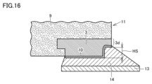
- Patent Document 1 when preparing a workpiece, there are cases where a workpiece is prepared in which a groove (recessed part) is formed in advance along the position where it is to be finally cut. . Due to the presence of the groove, for example, the plating film provided on the inner surface of the groove presents a concave space that is recessed inward after the lead frame is cut (in Patent Document 1, after the lead frame is singulated). A bonding material such as solder is guided into this concave space. For example, when mounting a semiconductor device on a substrate or the like, it becomes possible to bond solder well to both the lower and side surfaces of the leads, improving connection reliability.
- a method for manufacturing a workpiece according to the present disclosure includes a preparation step of preparing a workpiece including at least a lead frame in which a groove is formed in advance along a position to be cut, and before cutting the workpiece, a surface layer removal step of partially removing a surface layer portion forming the groove of the workpiece; and the workpiece from which the surface layer portion is partially removed before cutting the workpiece.
- an uncut region located between the cut region and the open end of the groove, and in the surface layer removal step at least a part of the uncut region is removed.
- a processed product manufacturing apparatus based on the present disclosure is a processed product manufacturing apparatus that performs processing on a workpiece that includes at least a lead frame in which a groove is formed in advance along a position to be cut, a surface layer removal unit that partially removes a surface layer portion of the workpiece forming the groove portion when the workpiece is not cut; , a plating processing unit that performs plating processing on the workpiece from which the surface layer portion has been partially removed, and in a state before the surface layer removal unit partially removes the surface layer portion, the surface layer portion includes a cutting region to be removed by cutting the workpiece, and a non-cutting region located between the cutting region and the open end of the groove, and the surface layer removal removing at least a portion of the uncut region.
- FIG. 13 is a sectional view corresponding to FIG. 12 and illustrating a surface layer removal process regarding a second modification of the embodiment.
- FIG. 13 is a sectional view corresponding to FIG. 12 and illustrating a surface layer removal process regarding a third modification of the embodiment. It is a figure which shows the manufacturing method of a processed product, and the manufacturing method of a semiconductor device using the same, regarding the 4th modification of embodiment. It is a figure which shows the manufacturing method of a processed product, and the manufacturing method of a semiconductor device using the same regarding the 5th modification of embodiment.
- FIG. 1 is a diagram showing a processed product manufacturing apparatus 20.
- the machined product manufacturing apparatus 20 processes a workpiece 22 held on a stage 21 . Grooves are previously formed in the workpiece 22 along the positions to be cut.
- the groove portion is a groove portion with a bottom, and is sometimes referred to as a bottomed groove.
- a groove 5 is formed in the lead frame 1, and the workpiece manufacturing apparatus 20 can function as a semiconductor device manufacturing apparatus. .
- the following description will be based on an example in which the processed product manufacturing apparatus 20 is a semiconductor device manufacturing apparatus.
- the emission section 23, the scanning section 24, and the control section 25 can function as a "surface layer removal section.”
- the surface layer removal section is a surface layer portion (in the lead frame 1) forming a groove (groove 5 in the lead frame 1 (see FIG. 4)) of the workpiece 22 in a state where the workpiece 22 is not cut.
- the surface layer portion 3c) is partially removed.
- the surface layer portion 3c of the lead frame 1 is partially removed by laser irradiation from the surface layer removal section.
- the plating processing unit 26 performs a plating process on the workpiece 22 (lead frame 1) from which the surface layer portion 3c has been partially removed while the workpiece 22 (lead frame 1) is not cut.
- FIG. 2 is a diagram showing a method for manufacturing a processed product and a method for manufacturing a semiconductor device using the same.
- the method for manufacturing a semiconductor device includes a preparation step ST10, a resin sealing step ST12, a resin removal step ST13, a surface layer removal step ST14, a plating step ST15, and a cutting step ST16.
- the preparation step ST10 includes a groove forming step ST11.
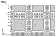
- FIG. 3 does not represent the cross-sectional structure of the lead frame 1, for convenience of illustration, hatching lines extending in an oblique direction are added to the portions forming the lead frame 1. Two types of hatching lines are used here, and the differences will be explained later. 3 to 5 illustrate a length direction S, a width direction W, and a height direction H for convenience of explanation, and in the following description, these directions will be referred to as appropriate. These directions are also appropriately illustrated in the drawings from FIG. 6 onwards.
- the lead frame 1 has a substantially plate-like shape that extends along both the length direction S and the width direction W.
- the lead frame 1 has a front surface 1a located on the side on which the semiconductor chip 6 (FIG. 6) is mounted, and a back surface 1b located on the opposite side to the front surface 1a, and is made of metal such as copper.
- Lead frame 1 includes a plurality of die pads 2, a plurality of lead parts 3, and a plurality of tie bars 4.
- the die pad 2 and the thick portion 3a are provided with hatching lines extending from the upper right side to the lower left side in the paper of FIG.
- the thin wall portion 3b of the lead portion 3 and the tie bar 4 are provided with hatching lines extending from the upper left side to the lower right side in the paper of FIG.
- the above-mentioned positive side surface of the tie bar 4 and the above-mentioned positive side surface of the thin-walled portion 3b of the lead portion 3 are recessed relative to the above-mentioned positive-side surface of the thick-walled portion 3a of the lead portion 3.
- the wires extend along the height direction H and the width direction W on the back surface 1b (FIG. 3) side of the tie bar 4, and the wires extend in the height direction H and the length direction S.
- a lattice-shaped groove portion 5 is formed extending along the groove.
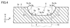
- the groove portion 5 does not penetrate through the lead frame 1 in the height direction H direction, but has a groove depth that is half the depth of the lead frame 1 (thick wall portion 3a), and the lead frame 1 is etched (wet etching). It can be formed by
- the groove width is, for example, 0.30 mm to 0.50 mm.
- the groove width and groove depth must be determined to ensure sufficient strength to prevent problems such as deformation in post-processing, to allow good appearance inspection in post-processing, and to ensure good mounting strength of the finished semiconductor device. Just take it into account and set it up.
- FIG. 6 is a cross-sectional view showing a state in which the semiconductor chip 6 is bonded onto the lead frame 1 (die pad 2) prepared in the preparation process. As shown in FIG. 6, a plurality of electrodes provided on each semiconductor chip 6 are electrically connected to the lead portion 3 (thick portion 3a) via the bonding wire 7.
- the protective film 8 is peeled off from the lead frame 1 before the resin removal step described below is performed. By removing the protective film 8, the resin material 9 (9b) formed in the groove 5 of the lead frame 1 is exposed. Note that the protective film 8 may be peeled off from the lead frame 1 before the laser marking process described with reference to FIG. 7.
- the pulse width it is possible to use a laser that generates a pulse width of nanoseconds, picoseconds, etc. Further, by controlling the emission section 23 and the scanning section 24 by the control section 25 (FIG. 1), the processing conditions by the laser beam L2 can be changed. Depending on the material of the resin material 9 (9b) and the size of the resin material 9 (9b) (groove width of the groove portion 5, etc.), the wavelength and output of the laser beam L2 are adjusted so that the resin material 9 (9b) can be removed efficiently. , laser focusing diameter, irradiation time, etc. are optimized.
- FIG. 10 is a cross-sectional view showing the surface layer removal process being performed.
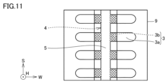
- FIG. 11 is a plan view for explaining the range in which the surface layer removal process is performed.
- the surface layer removal process is performed using a laser, for example.
- a short pulse less than picosecond oscillator.
- the surface layer removal step may be performed by other grinding means or other polishing means.
- the plated lead frame 1 is cut along the groove 5. As shown in FIG. In this cutting process, the entire thickness of the lead frame 1 and the resin material 9 is cut using the blade 12.
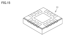
- semiconductor devices 11 As shown in FIG. 15, the semiconductor device 11 is a QFN (Quad Flat Non-leaded Package) type non-lead product in which electrical connection leads do not protrude outward from the product when viewed from above. be.
- QFN Quad Flat Non-leaded Package
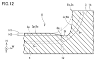
- the height H1 of the surface of the cutting area 3m is equal to the height H2 of the surface 3q of the boundary portion 3t, or at least a part of the cutting area 3m
- the height H1 of the surface is higher than the height H2 of the surface 3q of the boundary portion 3t. In the latter case, the height of the surface 3q of the boundary portion 3t is lower than the surface of at least a portion of the cutting area 3m.
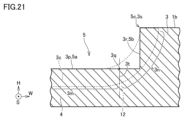
- FIG. 21 is a cross-sectional view corresponding to FIG. 12 for explaining the surface layer removal process regarding the third modification of the embodiment.
- the surface shape 3r of the non-cutting region 3n that is, the side portion 5b of the groove portion 5
- the surface shape 3r of the non-cutting region 3n may extend substantially parallel to the depth direction of the groove portion 5 (direction perpendicular to the back surface 1b).
Landscapes
- Lead Frames For Integrated Circuits (AREA)
- Physics & Mathematics (AREA)
- Geometry (AREA)
Abstract
Description
図1は、加工品の製造装置20を示す図である。加工品の製造装置20はステージ21上に保持された加工対象物22に対して加工を実施する。加工対象物22には、切断されるべき位置に沿って予め溝部が形成されている。ここで、溝部は、底がある溝部分であり、有底溝ということがある。加工対象物22が後述するリードフレーム1である場合、リードフレーム1には溝部5(図5等参照)が形成され、加工品の製造装置20は、半導体装置の製造装置として機能することができる。以下の説明では、加工品の製造装置20が半導体装置の製造装置である場合の例に基づいて説明を行なう。
図2は、加工品の製造方法、およびそれを使用する半導体装置の製造方法を示す図である。図1に示す加工品の製造装置20を使用して、半導体装置の製造方法を実施することができる。半導体装置の製造方法は、準備工程ST10、樹脂封止工程ST12、樹脂除去工程ST13、表層除去工程ST14、メッキ工程ST15、および切断工程ST16を備える。準備工程ST10は溝部形成工程ST11を有する。
準備工程ST10、表層除去工程ST14、およびメッキ工程ST15は、加工品の製造方法を構成することができる。すなわち、半導体装置の製造方法は加工品の製造方法を含み得る。以下、各工程について順に説明する。
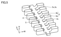
図3は、準備工程において準備されたリードフレーム1の裏面1b側から見た構成を示す平面図である。図4は、図3中のIV-IV線に沿った矢視断面図である。図5は、準備工程において準備されたリードフレーム1の一部(リード部3、タイバー4および溝部5)の裏面1b側から見た構成を示す斜視図である。
複数のダイパッド2は、長さ方向Sおよび幅方向Wの双方に間隔を空けて配列されている。ダイパッド2の表面1a上に、半導体チップ6が搭載される(図6参照)。複数のダイパッド2の各々の周囲(四方)に、複数のリード部3が矩形状に並んで配置されている。複数のダイパッド2の各々を取り囲むように、複数のタイバー4が格子状に配置されている。1つのタイバー4の両側に、複数のリード部3が設けられており、複数のリード部3は、タイバー4の延在方向に沿って間隔をあけて並んでいる。複数のリード部3の各々は、厚肉部3aと薄肉部3bとを有する(図3,図5)。リード部3においては、厚肉部3aが薄肉部3bを介してタイバー4に連結している。高さ方向Hにおいて、ダイパッド2および厚肉部3aは、薄肉部3bよりも大きな高さ寸法(すなわち厚み)を有する。
図5を参照して、ここで、タイバー4、リード部3の厚肉部3aおよび薄肉部3bについて、図5に示す「高さ方向Hの負側」に位置する表面に着目すると、これらの表面の高さ位置は同じである。一方で、図5に示す「高さ方向Hの正側」に位置する表面に着目すると、タイバー4の表面の高さ位置およびリード部3の薄肉部3bの表面の高さ位置よりも、リード部3の厚肉部3aの表面の高さ位置は、高い。
図6は、準備工程において準備されたリードフレーム1(ダイパッド2)上に、半導体チップ6がボンディングされた状態を示す断面図である。図6に示すように、各半導体チップ6に設けられた複数の電極が、ボンディングワイヤ7を介してリード部3(厚肉部3a)に電気的に接続される。
図9は、樹脂除去工程を行なっている様子を示す断面図である。樹脂除去工程においては、溝部5内の樹脂材9(9b)にレーザ光L2を照射し、レーザ光L2が長さ方向Sに沿って走査される。これにより、溝部5内の樹脂材が除去される。レーザ光L2としては、パルスレーザとして、たとえば、赤外レーザグリーンレーザ、もしくは、紫外レーザなどを利用可能である。
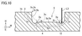
図10は、表層除去工程を行なっている様子を示す断面図である。図11は、表層除去工程を行なう範囲を説明するための平面図である。表層除去工程においては、リードフレーム1を切断する前に(換言すると、切断工程が行われる前に)、リードフレーム1のうちの溝部5を形成している表層部分3cを部分的に除去する。表層除去工程は、たとえばレーザを用いて行われる。リードフレーム1の材料(銅など)への高効率加工および熱影響抑制のため、短パルス(ピコ秒未満)の発振器を用いるとよい。表層除去工程は、他の研削手段または他の研磨手段などによって行われてもよい。
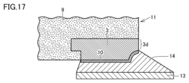
図13は、メッキ工程が行なわれた後の様子を示す断面図である。表層除去工程の実施後、リードフレーム1を切断する前に、表層部分3cが部分的に除去されたリードフレーム1にメッキ処理を行なう。リードフレーム1のダイパッド2の表面、リードフレーム1のタイバー4の表面、リード部3の薄肉部3bの表面、および表層部分3cのうちの表層除去工程が実施された表面に、メッキ層10が形成される。メッキ層10の形成によって、加工品の製造方法としては完了し、この時点のメッキ層10が形成されたリードフレーム1が「加工品」を構成することになる。
図14に示すように、メッキ処理が行なわれたリードフレーム1を溝部5に沿って切断する。この切断工程では、ブレード12を用いてリードフレーム1および樹脂材9の全厚さ部分を切断する。切断工程の実施により、複数の単位樹脂成形品としての半導体装置11が得られる。図15に示すように、半導体装置11は、平面視した場合に製品の外方に向けて電気的接続用のリードが突出していないQFN(Quad Flat Non-leaded Package)タイプのノンリード型の製品である。
図19は、図12に対応し、実施の形態の第1変形例に関する表層除去工程を説明するための断面図である。上述の例(図18等)では、非切断領域3nの少なくとも一部に加えて、切断領域3mの端部(図18に示す隙間3wに相当する部分)も除去される。このような構成は必須ではなく、図19に示すように、切断領域3mが平らになっていて溝部5の側部5bが切断領域3mに含まれない場合には、切断領域3mについては表層除去工程で除去しないようにしてもよい。はんだの誘導や接合に寄与する上記の凹所を形成するという目的は、非切断領域3nのみに表層除去工程を実施し、切断領域3mに表層除去工程を実施しないことによっても達成し得るものであり、切断領域3mに表層除去工程を実施しない分、製造時間の短縮化が図れる。
図20は、図12に対応し、実施の形態の第2変形例に関する表層除去工程を説明するための断面図である。表層除去工程が実施された後であって且つリードフレーム1が切断される前の状態において、切断領域3mの表面と非切断領域3nの表面とが相互に接続している部分(すなわち、境界部分3tの表面)は、平坦面の形状を呈しており、かつ、平坦面は、溝部5の深さ方向(裏面1bに対して直交する方向)に対して、略直交していてもよい。当該構成によっても、境界部分3tにおいてバリが発生することを小さくすることができる。
上述の通り、加工品の製造方法は、準備工程ST10、表層除去工程ST14、およびメッキ工程ST15は、加工品の製造方法を構成することができる。上述の実施の形態の場合(図2)には、表層除去工程ST14およびメッキ工程ST15が、樹脂除去工程ST13と切断工程ST16との間に行われる。
図23は、実施の形態の第5変形例に関する、加工品の製造方法、およびそれを使用する半導体装置の製造方法を示す図である。図23に示すように、加工品の製造方法に関するこれらの各工程は、連続して行われなくてもよい。準備工程ST10を実施した後に、表層除去工程ST14、樹脂封止工程ST12、樹脂除去工程ST13、メッキ工程ST15および切断工程ST16を順に実施してもよい。図23に示す例では、表層除去工程ST14が樹脂封止工程ST12よりも前の段階で行われ、メッキ工程ST15が樹脂除去工程ST13と切断工程ST16との間に行われる。
Claims (9)
- 加工品の製造方法であって、
切断されるべき位置に沿って予め溝部が形成されたリードフレームを少なくとも含む加工対象物を準備する準備工程と、
前記加工対象物を切断する前に、前記加工対象物のうちの前記溝部を形成している表層部分を部分的に除去する表層除去工程と、
前記加工対象物を切断する前に、前記表層部分が部分的に除去された前記加工対象物にメッキ処理を施すメッキ工程と、を含み、
前記表層除去工程が実施される前の状態において、前記表層部分は、前記加工対象物が切断されることにより除去されることとなる切断領域と、前記切断領域と前記溝部の開口端との間に位置する非切断領域と、を含んでおり、
前記表層除去工程においては、前記非切断領域の少なくとも一部を除去する、
加工品の製造方法。 - 前記表層除去工程においては、前記非切断領域の前記少なくとも一部に加え、前記切断領域のうちの前記非切断領域寄りの部分も除去する、
請求項1に記載の加工品の製造方法。 - 前記表層除去工程が実施される前の状態において、前記非切断領域の表面形状は、前記溝部の底部に近づくほど前記溝部の前記開口端よりも溝幅方向の中央寄りに位置するように湾曲している、
請求項1または2に記載の加工品の製造方法。 - 前記表層除去工程が実施された後であって且つ前記加工対象物が切断される前の状態において、前記表層部分は、前記切断領域と前記非切断領域との間に境界部分を含んでおり、
前記溝部の深さ方向における前記表層部分の表面の位置を高さと定義した場合、
前記表層除去工程が実施された後であって且つ前記加工対象物が切断される前の状態において、前記切断領域のうちの少なくとも一部の表面の高さは、前記境界部分の表面の高さよりも高い、
請求項1から3のいずれか1項に記載の加工品の製造方法。 - 前記表層除去工程が実施された後であって且つ前記加工対象物が切断される前の状態において、前記切断領域の表面と前記非切断領域の表面とが相互に接続している部分は、平坦面の形状を呈しており、
前記平坦面は、前記溝部の深さ方向に対して略直交している、
請求項1から4のいずれか1項に記載の加工品の製造方法。 - 前記表層除去工程は、レーザを用いて行われる、
請求項1から5のいずれか1項に記載の加工品の製造方法。 - 前記準備工程において準備された前記加工対象物は、ウェットエッチングによって形成された前記溝部を有している、
請求項1から6のいずれか1項に記載の加工品の製造方法。 - 請求項1から7のいずれか1項に記載の加工品の製造方法を使用する、半導体装置の製造方法であって、
前記リードフレームに半導体チップがボンディングされた状態で、前記リードフレームおよび前記半導体チップを樹脂材により封止する樹脂封止工程と、
前記溝部内の前記樹脂材を除去する樹脂除去工程と、
前記リードフレームを、前記溝部に沿って切断する切断工程と、を含み、
前記加工品の製造方法としては、
前記表層除去工程および前記メッキ工程が、前記樹脂除去工程と前記切断工程との間に行われるか、
前記表層除去工程および前記メッキ工程が、前記樹脂封止工程よりも前の段階で行われるか、または、
前記表層除去工程が前記樹脂封止工程よりも前の段階で行われ、前記メッキ工程が前記樹脂除去工程と前記切断工程との間に行われる、
半導体装置の製造方法。 - 切断されるべき位置に沿って予め溝部が形成されたリードフレームを少なくとも含む加工対象物に対して加工を実施する、加工品の製造装置であって、
前記加工対象物が切断されていない状態で、前記加工対象物のうちの前記溝部を形成している表層部分を部分的に除去する表層除去部と、
前記加工対象物が切断されていない状態で、前記表層部分が部分的に除去された前記加工対象物にメッキ処理を施すメッキ処理部と、を備え、
前記表層除去部が前記表層部分を部分的に除去する前の状態において、前記表層部分は、前記加工対象物が切断されることにより除去されることとなる切断領域と、前記切断領域と前記溝部の開口端との間に位置する非切断領域と、を含んでおり、
前記表層除去部は、前記非切断領域の少なくとも一部を除去する、
加工品の製造装置。
Priority Applications (2)
| Application Number | Priority Date | Filing Date | Title |
|---|---|---|---|
| KR1020247026492A KR102883592B1 (ko) | 2022-03-28 | 2022-12-15 | 가공품의 제조 방법, 반도체 장치의 제조 방법, 및 가공품의 제조 장치 |
| CN202280091674.XA CN118696413A (zh) | 2022-03-28 | 2022-12-15 | 加工品的制造方法、半导体装置的制造方法、及加工品的制造装置 |
Applications Claiming Priority (2)
| Application Number | Priority Date | Filing Date | Title |
|---|---|---|---|
| JP2022051327A JP7705818B2 (ja) | 2022-03-28 | 2022-03-28 | 加工品の製造方法、半導体装置の製造方法、および加工品の製造装置 |
| JP2022-051327 | 2022-03-28 |
Publications (1)
| Publication Number | Publication Date |
|---|---|
| WO2023188587A1 true WO2023188587A1 (ja) | 2023-10-05 |
Family
ID=88200034
Family Applications (1)
| Application Number | Title | Priority Date | Filing Date |
|---|---|---|---|
| PCT/JP2022/046171 Ceased WO2023188587A1 (ja) | 2022-03-28 | 2022-12-15 | 加工品の製造方法、半導体装置の製造方法、および加工品の製造装置 |
Country Status (5)
| Country | Link |
|---|---|
| JP (1) | JP7705818B2 (ja) |
| KR (1) | KR102883592B1 (ja) |
| CN (1) | CN118696413A (ja) |
| TW (1) | TWI842386B (ja) |
| WO (1) | WO2023188587A1 (ja) |
Citations (5)
| Publication number | Priority date | Publication date | Assignee | Title |
|---|---|---|---|---|
| JP2008186891A (ja) * | 2007-01-29 | 2008-08-14 | Denso Corp | モールドパッケージおよびその製造方法ならびにモールドパッケージの実装構造 |
| WO2015145651A1 (ja) * | 2014-03-27 | 2015-10-01 | ルネサスエレクトロニクス株式会社 | 半導体装置の製造方法および半導体装置 |
| JP2021061266A (ja) * | 2019-10-02 | 2021-04-15 | 大口マテリアル株式会社 | リードフレーム |
| JP2021125611A (ja) * | 2020-02-06 | 2021-08-30 | 新光電気工業株式会社 | リードフレーム、半導体装置及びリードフレームの製造方法 |
| US20210299791A1 (en) * | 2020-03-27 | 2021-09-30 | Integrated Silicon Solution Inc. | Method of forming package structure |
Family Cites Families (2)
| Publication number | Priority date | Publication date | Assignee | Title |
|---|---|---|---|---|
| JP2011077278A (ja) | 2009-09-30 | 2011-04-14 | Sanyo Electric Co Ltd | 半導体装置およびその製造方法 |
| JP6827495B2 (ja) * | 2019-05-16 | 2021-02-10 | Towa株式会社 | 半導体装置の製造方法 |
-
2022
- 2022-03-28 JP JP2022051327A patent/JP7705818B2/ja active Active
- 2022-12-15 KR KR1020247026492A patent/KR102883592B1/ko active Active
- 2022-12-15 WO PCT/JP2022/046171 patent/WO2023188587A1/ja not_active Ceased
- 2022-12-15 CN CN202280091674.XA patent/CN118696413A/zh active Pending
-
2023
- 2023-02-13 TW TW112104895A patent/TWI842386B/zh active
Patent Citations (5)
| Publication number | Priority date | Publication date | Assignee | Title |
|---|---|---|---|---|
| JP2008186891A (ja) * | 2007-01-29 | 2008-08-14 | Denso Corp | モールドパッケージおよびその製造方法ならびにモールドパッケージの実装構造 |
| WO2015145651A1 (ja) * | 2014-03-27 | 2015-10-01 | ルネサスエレクトロニクス株式会社 | 半導体装置の製造方法および半導体装置 |
| JP2021061266A (ja) * | 2019-10-02 | 2021-04-15 | 大口マテリアル株式会社 | リードフレーム |
| JP2021125611A (ja) * | 2020-02-06 | 2021-08-30 | 新光電気工業株式会社 | リードフレーム、半導体装置及びリードフレームの製造方法 |
| US20210299791A1 (en) * | 2020-03-27 | 2021-09-30 | Integrated Silicon Solution Inc. | Method of forming package structure |
Also Published As
| Publication number | Publication date |
|---|---|
| TWI842386B (zh) | 2024-05-11 |
| CN118696413A (zh) | 2024-09-24 |
| JP7705818B2 (ja) | 2025-07-10 |
| JP2023144386A (ja) | 2023-10-11 |
| TW202339132A (zh) | 2023-10-01 |
| KR20240132490A (ko) | 2024-09-03 |
| KR102883592B1 (ko) | 2025-11-07 |
Similar Documents
| Publication | Publication Date | Title |
|---|---|---|
| JP6827495B2 (ja) | 半導体装置の製造方法 | |
| WO2023188587A1 (ja) | 加工品の製造方法、半導体装置の製造方法、および加工品の製造装置 | |
| TWI829258B (zh) | 半導體裝置以及其製造方法 | |
| KR102937027B1 (ko) | 반도체 장치의 제조 방법 및 리드 프레임 | |
| TWI878743B (zh) | 雷射加工裝置、雷射加工方法、及半導體裝置的製造方法 | |
| JP2969054B2 (ja) | 半導体装置の製造方法及び半導体装置 | |
| JPH08236574A (ja) | 半導体装置の組立方法 | |
| CN121888970A (zh) | Qfn封装器件及其形成方法 | |
| JP2002289757A (ja) | 電子部品のリード切断方法 | |
| JP2001093921A (ja) | 半導体装置の製造方法 | |
| JPH077113A (ja) | リードフレームの製造方法及びリードフレーム | |
| JP2022177326A (ja) | 半導体素子、および半導体素子の製造方法 | |
| JPH06302738A (ja) | 金属板の加工方法及びリードフレームの加工方法並びに金属板及びリードフレーム | |
| JPH03238842A (ja) | 半導体装置の製造方法 |
Legal Events
| Date | Code | Title | Description |
|---|---|---|---|
| 121 | Ep: the epo has been informed by wipo that ep was designated in this application |
Ref document number: 22935715 Country of ref document: EP Kind code of ref document: A1 |
|
| ENP | Entry into the national phase |
Ref document number: 20247026492 Country of ref document: KR Kind code of ref document: A |
|
| WWE | Wipo information: entry into national phase |
Ref document number: 202280091674.X Country of ref document: CN |
|
| NENP | Non-entry into the national phase |
Ref country code: DE |
|
| WWE | Wipo information: entry into national phase |
Ref document number: 11202404895R Country of ref document: SG |
|
| 122 | Ep: pct application non-entry in european phase |
Ref document number: 22935715 Country of ref document: EP Kind code of ref document: A1 |