WO2023176663A1 - Composant électronique - Google Patents
Composant électronique Download PDFInfo
- Publication number
- WO2023176663A1 WO2023176663A1 PCT/JP2023/008978 JP2023008978W WO2023176663A1 WO 2023176663 A1 WO2023176663 A1 WO 2023176663A1 JP 2023008978 W JP2023008978 W JP 2023008978W WO 2023176663 A1 WO2023176663 A1 WO 2023176663A1
- Authority
- WO
- WIPO (PCT)
- Prior art keywords
- plate
- electronic component
- component according
- thickness
- hole
- Prior art date
Links
Images


Classifications
-
- H—ELECTRICITY
- H01—ELECTRIC ELEMENTS
- H01G—CAPACITORS; CAPACITORS, RECTIFIERS, DETECTORS, SWITCHING DEVICES OR LIGHT-SENSITIVE DEVICES, OF THE ELECTROLYTIC TYPE
- H01G2/00—Details of capacitors not covered by a single one of groups H01G4/00-H01G11/00
- H01G2/10—Housing; Encapsulation
-
- H—ELECTRICITY
- H01—ELECTRIC ELEMENTS
- H01G—CAPACITORS; CAPACITORS, RECTIFIERS, DETECTORS, SWITCHING DEVICES OR LIGHT-SENSITIVE DEVICES, OF THE ELECTROLYTIC TYPE
- H01G9/00—Electrolytic capacitors, rectifiers, detectors, switching devices, light-sensitive or temperature-sensitive devices; Processes of their manufacture
- H01G9/004—Details
- H01G9/08—Housing; Encapsulation
Definitions
- the present invention relates to electronic components.
- the functional parts are sealed using materials such as resin, metal, or glass in order to protect the functional parts from moisture in the usage environment.
- WO 2006/000001 discloses a carrier element (3), at least one optoelectronic element (2) mounted on the carrier element (3) and a cover (5) for the optoelectronic element (2).
- An optoelectronic module (1) is disclosed having: a cavity (11);
- the cover (5) has a frame (7) which completely surrounds the optoelectronic element (2) in the circumferential direction and which is connected to the support element (3) and which directs electromagnetic radiation into the cover (5).
- a glass element (9, 90) The cavity (11) is formed inside a volume defined at least partially by the inner surface of the cover (5) and the surface of the support element (3).
- the optoelectronic component (2) is arranged in the cavity (11) in such a way that it is hermetically and/or autoclavably enclosed by the cover (5).
- the optoelectronic module (1) has a filling material (13) that at least partially fills the cavity (11).
- the optoelectronic module (1) is configured and formed to compensate for the expansion of the volume occupied by the filling material (13) and has for this purpose at least one first compensating volume (15) which is deformable. .
- WO 2006/000001 discloses that bonding the cover (5) to the support element (3) in order to hermetically and/or autoclavably encapsulate the optoelectronic element (2) can be carried out by one of the following processes: to be carried out by one person, i.e.
- the support element (3) is preferably ceramic or metal
- the frame (7) is preferably ceramic or metal, in particular metal coated with glass
- ⁇ Resistance welding, - soldering with metal solder in which case the support element (3) and the cover (5) each have a surface suitable for establishing a firm bond with the solder, preferably a surface with a solder preform has ⁇ Soldering using glass solder, adhesion of at least the frame (7) and the glass element (9), the adhesion of the frame (7) and the support element (3), or the glass element (9) and the support element, using a filler material (13); (3) Adhesion with adhesion of at least the frame (7) and the glass element (9), the adhesion of the frame (7) and the support element (3) with a silicone, polymer or bonding material different from the filler material (13); or It is stated that this is carried out by one of gluing the glass element (9) and the support element (3).
- the present invention has been made in order to solve the above problems, and an object of the present invention is to provide an electronic component that can suppress the infiltration of moisture into functional parts.
- the electronic component of the present invention includes a first plate having a first main surface and a second main surface facing each other in the thickness direction, and a side surface connecting the first main surface and the second main surface; a lid portion disposed apart from the first plate so as to face the first principal surface of the first plate in the thickness direction; and an internal space hermetically sealed together with the first plate and the lid portion.
- a sealing body including: a sealing metal layer; a functional section provided in an internal space of the sealing body spaced apart from the first plate; and a functional section to which a potential is applied to a pair of electrodes; and the functional section; a first through-hole passing through the first plate in the thickness direction; a via conductor provided inside the second through hole communicating with the through hole and electrically connected to the pair of electrodes of the functional section.
- the lid portion has a water vapor permeability of 1/10 or less when compared to the filled resin portion having the same film thickness, or the lid portion is made of glass or metal.
- the first plate is a glass plate.
- the sealing metal layer is provided in direct connection with the first plate.
- FIG. 1 is a cross-sectional view schematically showing an example of the electronic component of the present invention.
- FIG. 2 is a cross-sectional view schematically showing an example of an electronic component whose functional part is a capacitor.
- FIG. 3 is an enlarged view of the portion indicated by III in FIG.
- FIG. 4 is an enlarged view of the portion indicated by IV in FIG.
- FIG. 5 is a cross-sectional view schematically showing an example of an electronic component in which the central axis of the first through hole does not coincide with the central axis of the second through hole.
- FIG. 6 is a cross-sectional view schematically showing a first modification of the electronic component shown in FIG.
- FIG. 7 is a cross-sectional view schematically showing a second modification of the electronic component shown in FIG. FIG.
- FIG. 8 is a cross-sectional view schematically showing a modification of the electronic component shown in FIG. 7.
- FIG. 9 is a cross-sectional view schematically showing a modification of the electronic component shown in FIG. 2.
- FIG. 10 is a cross-sectional view schematically showing an electronic component according to an example.
- FIG. 11 is an enlarged view of the portion indicated by XI in FIG.
- the present invention is not limited to the following configuration, and can be modified and applied as appropriate without changing the gist of the present invention.
- the present invention also includes a combination of two or more of the individual preferred configurations of the present invention described below.
- the surface of the filled resin part that seals the functional part is covered with a sealing body.
- the first plate, the lid part, and the sealing metal layer included in the sealing body are made of a material that is less permeable to moisture than the filling resin part, and the sealing metal layer is provided in direct connection with the first plate. By doing so, it is possible to suppress moisture from entering the functional part.
- wiring can be drawn out from the functional section via a via conductor or the like provided inside the through hole penetrating the glass plate and the filled resin section.
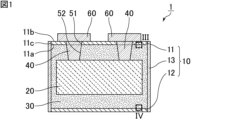
- FIG. 1 is a cross-sectional view schematically showing an example of the electronic component of the present invention.
- the electronic component 1 shown in FIG. 1 includes a sealing body 10, a functional section 20, a filled resin section 30, and a via conductor 40.
- the sealing body 10 includes a first plate 11, a lid portion 12, and a sealing metal layer 13.
- the first plate 11 has a first main surface 11a and a second main surface 11b that face each other in the thickness direction, and a side surface 11c that connects the first main surface 11a and the second main surface 11b.
- the lid portion 12 is spaced apart from the first plate 11 so as to face the first main surface 11a of the first plate 11 in the thickness direction.
- the sealing metal layer 13 hermetically seals the internal space of the sealing body 10 together with the first plate 11 and the lid part 12.
- the functional section 20 is provided in the internal space of the sealing body 10 and separated from the first plate 11. In the functional section 20, a potential is applied to a pair of electrodes (not shown).
- the filling resin part 30 is filled between the sealing body 10 and the functional part 20.
- the via conductor 40 is connected to the inside of a first through hole 51 that penetrates the first plate 11 in the thickness direction, and the inside of a second through hole 52 that penetrates the filled resin part 30 in the thickness direction and communicates with the first through hole 51. It is set up at The via conductor 40 is electrically connected to a pair of electrodes of the functional section 20 (for example, a pair of electrodes located on the upper surface side of the functional section 20).
- the central axis of the first through hole 51 coincides with the central axis of the second through hole 52, so the via conductor 40 is provided in a straight line.
- the cross-sectional shape of the first through hole 51 and the second through hole 52 viewed from the thickness direction is not particularly limited, and examples thereof include polygons such as quadrangles, circles, ellipses, and the like.
- the first through hole 51 and the second through hole 52 may have a taper in which the hole diameter becomes smaller in the thickness direction toward the functional part 20.
- the pore diameter refers to the diameter when the cross-sectional shape is circular, and the maximum length passing through the center of the cross-section when the cross-sectional shape is other than circular.
- the via conductors 40 provided inside the first through hole 51 and the second through hole 52 only need to be provided on at least the inner wall surfaces of the first through hole 51 and the second through hole 52.
- the inner wall surfaces of the first through hole 51 and the second through hole 52 are metalized with a low resistance metal such as copper, gold, or silver.
- the metallization of the via conductor 40 is not limited to the case where only the inner wall surfaces of the first through hole 51 and the second through hole 52 are metalized, but metal or a composite material of metal and resin, etc.
- the second through hole 52 may be filled with the second through hole 52.
- the via conductor 40 may be a through-hole conductor that penetrates the sealing body 10 in the thickness direction.
- a through-hole conductor that is not electrically connected to the pair of electrodes of the functional section 20 is provided. Good too. Such a through-hole conductor simply functions as a wiring.
- a through-hole conductor that is not electrically connected to the pair of electrodes of the functional part 20 may be provided so as to penetrate the sealing body 10 in the thickness direction without passing through the functional part 20, and the through-hole conductor may be provided so as to penetrate the sealing body 10 in the thickness direction without passing through the functional part 20. It may be provided so as to penetrate the stopper 10 in the thickness direction. Note that when a through-hole conductor is provided to penetrate the sealing body 10 including the functional part 20 in the thickness direction, an insulating material is filled between the through-hole penetrating the functional part 20 and the through-hole conductor. Ru.
- a wiring 60 electrically connected to the via conductor 40 is provided on the second main surface 11b of the first plate 11.
- the portion of the wiring 60 that is connected to the via conductor 40 may be a land.
- the wiring 60 is mainly composed of a low-resistance metal such as copper, gold, or silver.
- the first plate 11 is a glass plate.
- the water vapor permeability of the lid portion 12 is one-tenth or less when compared to the filled resin portion 30 having the same film thickness.
- Water vapor permeability can be measured, for example, according to JIS K 7129 "Plastics - Films and sheets - How to determine water vapor permeability (gas chromatography method)".
- the water vapor permeability of the lid part 12 should be one-tenth or less of the water vapor permeability of the filled resin part 30.
- the lid part 12 has a water vapor permeability of 1/10 to 1/10 (1/10,000,000,000) or more when compared to, for example, the filled resin part 30 having the same film thickness.
- the lid portion 12 is made of glass or metal, for example.
- the lid part 12 is, for example, a glass plate.
- the glass constituting the lid portion 12 may be the same as or different from the glass constituting the first plate 11.
- a via conductor (which may be a through-hole conductor) may be provided similarly to the first plate 11.
- the via conductor provided in the lid part 12 is connected to the inside of the first through hole that penetrates the lid part 12 in the thickness direction, and the second through hole that penetrates the filled resin part 30 in the thickness direction and communicates with the first through hole. It is provided inside the through hole and electrically connected to a pair of electrodes of the functional section 20 (for example, a pair of electrodes located on the lower surface side of the functional section 20).
- wiring electrically connected to the via conductor be provided on the main surface of the lid portion 12 on the opposite side from the filled resin portion 30.
- the portion of the wiring that is connected to the via conductor may be a land.
- the lid part 12 When the lid part 12 is made of metal, the lid part 12 has the same configuration as the sealing metal layer 13, for example.
- the metal forming the lid portion 12 may be the same as or different from the metal forming the sealing metal layer 13.
- the sealing metal layer 13 is provided in direct connection to the first plate 11. In this case, it is preferable that the sealing metal layer 13 is directly bonded to the first plate 11.
- the sealing metal layer 13 is preferably provided in direct connection with the side surface 11c of the first plate 11. In this case, it is preferable that the sealing metal layer 13 is directly bonded to the side surface 11c of the first plate 11.
- the sealing metal layer 13 is provided in direct connection with the lid part 12. In this case, it is preferable that the sealing metal layer 13 is directly bonded to the lid part 12.
- the sealing metal layer 13 is preferably provided in direct connection with the side surface of the lid portion 12. In this case, it is preferable that the sealing metal layer 13 is directly adhered to the side surface of the lid part 12.
- the sealing metal layer 13 includes, for example, a base layer and a plating layer from the filled resin part 30 side.
- the base layer may be one layer or two or more layers.
- the number of plating layers may be one, or two or more.
- the base layer is formed, for example, by sputtering or electroless plating.
- the base layer includes, for example, an adhesion layer and a power supply layer from the filled resin part 30 side.
- the plating layer is formed by electrolytic plating, for example.
- the filled resin portion 30 is made of resin having insulation properties.
- the resin constituting the filled resin portion 30 include insulating resins such as epoxy resin and phenol resin.
- the filled resin part 30 contains a filler.
- the filler included in the filled resin portion 30 include inorganic fillers such as silica particles, alumina particles, and metal particles.
- the filled resin portion 30 may be composed of only one resin layer, or may be composed of two or more resin layers laminated in the thickness direction.
- the materials constituting each resin layer may be the same or different.
- FIG. 2 is a cross-sectional view schematically showing an example of an electronic component whose functional part is a capacitor.
- the functional section 20 includes an anode plate 21 made of metal.
- the anode plate 21 has a core portion 22 made of valve metal. It is preferable that the anode plate 21 has a porous portion 23 provided on at least one main surface of the core portion 22 .
- a dielectric layer (not shown) is provided on the surface of the porous portion 23, and a cathode layer 24 is provided on the surface of the dielectric layer.
- the functional section 20 forms a capacitor such as a conductive polymer capacitor.
- one via conductor 40 is electrically connected to the core 22 of the anode plate 21, and the other via conductor 40 is electrically connected to the cathode layer 24. Therefore, the core portion 22 of the anode plate 21 and the cathode layer 24 correspond to "a pair of electrodes of the functional section 20.”
- the via conductor 40 may be a through-hole conductor that penetrates the sealing body 10 in the thickness direction.
- a through-hole conductor electrically connected to the core portion 22 of the anode plate 21 is provided so as to penetrate the sealing body 10 including the functional portion 20 in the thickness direction.
- the structure is such that the core portion 22 of the anode plate 21 and the through-hole conductor are directly connected.
- the anode plate 21 is made of a valve metal that exhibits a so-called valve action.
- valve metals include simple metals such as aluminum, tantalum, niobium, titanium, and zirconium, and alloys containing at least one of these metals. Among these, aluminum or aluminum alloy is preferred.
- the shape of the anode plate 21 is preferably flat, and more preferably foil-like.
- the anode plate 21 only needs to have the porous portion 23 on at least one main surface of the core portion 22, and may have the porous portion 23 on both main surfaces of the core portion 22.
- the porous portion 23 is preferably a porous layer formed on the surface of the core portion 22, and more preferably an etched layer.
- the dielectric layer provided on the surface of the porous portion 23 is porous reflecting the surface condition of the porous portion 23, and has a finely uneven surface shape.
- the dielectric layer is preferably made of an oxide film of the valve metal.
- the surface of the aluminum foil is anodized (also referred to as chemical conversion treatment) in an aqueous solution containing ammonium adipate, etc. to form a dielectric layer made of an oxide film. can be formed.
- the cathode layer 24 provided on the surface of the dielectric layer includes, for example, a solid electrolyte layer provided on the surface of the dielectric layer.
- the cathode layer 24 further includes a conductor layer provided on the surface of the solid electrolyte layer.
- the material constituting the solid electrolyte layer examples include conductive polymers such as polypyrroles, polythiophenes, and polyanilines. Among these, polythiophenes are preferred, and poly(3,4-ethylenedioxythiophene) called PEDOT is particularly preferred. Further, the conductive polymer may contain a dopant such as polystyrene sulfonic acid (PSS). Note that the solid electrolyte layer preferably includes an inner layer that fills the pores (recesses) of the dielectric layer and an outer layer that covers the dielectric layer.
- conductive polymers such as polypyrroles, polythiophenes, and polyanilines. Among these, polythiophenes are preferred, and poly(3,4-ethylenedioxythiophene) called PEDOT is particularly preferred.
- the conductive polymer may contain a dopant such as polystyrene sulfonic acid (PSS).
- PSS polystyrene sulfonic acid
- the conductor layer includes at least one of a conductive resin layer and a metal layer.
- the conductor layer may be only a conductive resin layer or only a metal layer.
- the conductor layer preferably covers the entire surface of the solid electrolyte layer.
- the conductive resin layer examples include a conductive adhesive layer containing at least one conductive filler selected from the group consisting of silver filler, copper filler, nickel filler, and carbon filler.
- the metal layer examples include metal plating films, metal foils, and the like.
- the metal layer is preferably made of at least one metal selected from the group consisting of nickel, copper, silver, and alloys containing these metals as main components. Note that the term "main component" refers to an elemental component having the largest elemental weight ratio.
- the conductor layer includes, for example, a carbon layer provided on the surface of the solid electrolyte layer and a copper layer provided on the surface of the carbon layer.
- the carbon layer is provided to electrically and mechanically connect the solid electrolyte layer and the copper layer.
- the carbon layer can be formed in a predetermined area by applying carbon paste onto the solid electrolyte layer by a method such as sponge transfer, screen printing, dispenser coating, or inkjet printing.
- the copper layer can be formed in a predetermined area by applying a copper paste onto the carbon layer by a method such as sponge transfer, screen printing, spray coating, dispenser coating, or inkjet printing.
- the functional unit 20 is a capacitor
- a ceramic capacitor using barium titanate or a thin film capacitor using silicon nitride (SiN), silicon dioxide (SiO 2 ), hydrogen fluoride (HF), etc. is used as the capacitor. It is also possible.
- the functional part 20 is a capacitor based on a metal such as aluminum. A conductive polymer capacitor whose base material is a metal such as aluminum is more preferable.
- Examples of the functional unit 20 that requires moisture resistance include capacitors such as conductive polymer capacitors and high dielectric constant thin film capacitors, batteries such as all-solid-state batteries, and lithium ion secondary batteries (LIBs).
- capacitors such as conductive polymer capacitors and high dielectric constant thin film capacitors
- batteries such as all-solid-state batteries
- LIBs lithium ion secondary batteries
- FIG. 3 is an enlarged view of the portion indicated by III in FIG. 1.
- a first adhesive layer 14 is provided between the filled resin part 30 and the first plate 11.
- the first adhesive layer 14 can improve the adhesion between the filled resin part 30 and the first plate 11.
- the first adhesive layer 14 has insulation and adhesive properties.
- the first adhesive layer 14 is made of, for example, an epoxy adhesive sheet, an epoxy adhesive, an acrylic adhesive sheet, an acrylic adhesive, or the like.
- the first adhesive layer 14 may be provided on the entire surface between the filled resin portion 30 and the first plate 11, or may be provided on a portion thereof.
- the Young's modulus of the first adhesive layer 14 is preferably lower than the Young's modulus of the first plate 11 and lower than the Young's modulus of the filled resin portion 30. In this case, when the filled resin portion 30 thermally expands, the first adhesive layer 14 can absorb the thermal expansion of the filled resin portion 30.
- the Young's modulus of the first adhesive layer 14 is, for example, 0.005 GPa or more and 2.9 GPa or less.
- the Young's modulus of the first plate 11 is, for example, 50 GPa or more and 90 GPa or less.
- the Young's modulus of the filled resin portion 30 is, for example, 3 GPa or more and 50 GPa or less.
- Young's modulus can be measured, for example, by a static test method (bending test).
- the thickness of the first plate 11 is preferably 200 ⁇ m or less. In this case, thermal expansion of the filled resin portion 30 can be allowed by deformation of the first plate 11.
- the thickness of the first plate 11 is preferably 5 ⁇ m or more from the viewpoint of ensuring the mechanical strength of the first plate 11.
- the thickness of the first plate 11 means the dimension of the first plate 11 in the thickness direction of the first plate 11.
- the thickness of the sealing metal layer 13 is preferably four times or less the thickness of the first plate 11, and more preferably thinner than the thickness of the first plate 11. preferable. In this case, thermal expansion of the filled resin portion 30 can be tolerated by deforming both the first plate 11 and the sealing metal layer 13.
- the thickness of the sealing metal layer 13 is preferably 10 ⁇ m or more from the viewpoint of suppressing moisture from entering the functional section 20.
- the thickness of the sealing metal layer 13 means the dimension of the sealing metal layer 13 in a direction parallel to the main surface of the first plate 11.
- the lid portion 12 is plate-shaped, and the thickness of the lid portion 12 is preferably 200 ⁇ m or less. In this case, the thermal expansion of the filled resin part 30 can also be allowed by deformation of the lid part 12.
- the thickness of the lid part 12 is preferably 5 ⁇ m or more from the viewpoint of ensuring the mechanical strength of the lid part 12. Note that the thickness of the lid portion 12 may be the same as or different from the thickness of the first plate 11.
- the thickness of the lid 12 means the dimension of the lid 12 in the thickness direction of the first plate 11.
- FIG. 4 is an enlarged view of the portion indicated by IV in FIG. 1.
- the second adhesive layer 15 is provided between the filled resin part 30 and the lid part 12, as shown in FIG.
- the adhesion between the filled resin part 30 and the lid part 12 can be improved by the second adhesive layer 15.
- the second adhesive layer 15 has insulation and adhesive properties.
- the second adhesive layer 15 is made of, for example, an epoxy adhesive sheet, an epoxy adhesive, an acrylic adhesive sheet, an acrylic adhesive, or the like.
- the second adhesive layer 15 may be provided on the entire surface between the filled resin portion 30 and the lid portion 12, or may be provided on a portion thereof.
- the material of the second adhesive layer 15 may be the same as or different from the material of the first adhesive layer 14.
- the Young's modulus of the second adhesive layer 15 is preferably lower than the Young's modulus of the lid portion 12 and lower than the Young's modulus of the filled resin portion 30. In this case, when the filled resin portion 30 thermally expands, the second adhesive layer 15 can absorb the thermal expansion of the filled resin portion 30.
- the Young's modulus of the second adhesive layer 15 is, for example, 0.005 GPa or more and 2.9 GPa or less.
- the Young's modulus of the second adhesive layer 15 may be the same as or different from the Young's modulus of the first adhesive layer 14.
- the Young's modulus of the lid part 12 is, for example, 50 GPa or more and 90 GPa or less.
- the Young's modulus of the lid 12 may be the same as or different from the Young's modulus of the first plate 11.
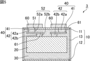
- FIG. 5 is a cross-sectional view schematically showing an example of an electronic component in which the central axis of the first through hole does not coincide with the central axis of the second through hole.
- the central axis of the first through hole 51 does not coincide with the central axis of the second through hole 52.
- the second through hole 52 includes a second through hole 52a on the first plate 11 side and a second through hole 52b on the functional part 20 side, and the central axis of the first through hole 51 does not coincide with the central axis of the second through hole 52b on the functional section 20 side.
- the central axis of the second through hole 52a on the first plate 11 side does not match the central axis of the second through hole 52b on the functional part 20 side.
- the central axis of the first through hole 51 may coincide with the central axis of the second through hole 52a on the first plate 11 side, or may coincide with the central axis of the second through hole 52a on the first plate 11 side. You don't have to.
- the via conductor 40 includes a first via conductor 41 provided inside the first through hole 51 and a second via conductor 42 provided inside the second through hole 52.
- the central axis of the first via conductor 41 is located on the side of the central axis of the second via conductor 42.
- the first via conductor 41 and the second via conductor 42 are electrically connected by a wiring 61 provided in the filled resin part 30.
- the second via conductor 42 includes a second via conductor 42a provided inside the second through hole 52a on the first plate 11 side, and a second via conductor 42a provided inside the second through hole 52b on the functional part 20 side.
- the center axis of the first via conductor 41 is located on the side of the center axis of the second via conductor 42b on the functional section 20 side.
- the central axis of the second via conductor 42a on the first plate 11 side is located on the side of the central axis of the second via conductor 42b on the functional section 20 side.
- the central axis of the first via conductor 41 may coincide with the central axis of the second via conductor 42a on the first plate 11 side, and is located to the side of the central axis of the second via conductor 42a on the first plate 11 side. You may.
- the via conductor 40 is divided into a first via conductor 41 and a second via conductor 42 so that the first via conductor 41 and the second via conductor 42 are not lined up in a straight line. This makes it possible to alleviate the stress applied to the first plate 11 when the via conductor 40 thermally expands in the thickness direction.
- the first via conductor 41 does not overlap with the second via conductor 42 when viewed from the thickness direction.
- the first via conductor 41 does not overlap the second via conductor 42b on the functional section 20 side when viewed from the thickness direction.
- the first via conductor 41 may or may not overlap the second via conductor 42a on the first plate 11 side.
- the second via conductor 42a on the first plate 11 side may or may not overlap with the second via conductor 42b on the functional section 20 side.
- the wiring 61 only needs to be placed between the first plate 11 and the functional section 20.
- the wiring 61 is arranged apart from the first plate 11 and the functional section 20, but the wiring 61 may be arranged so as to be in contact with the first plate 11, for example.
- the second via conductor 42 does not include the second via conductor 42a on the first plate 11 side, but only the second via conductor 42b on the functional part 20 side. include.
- the wiring 61 between the first via conductor 41 and the second via conductor 42 is mainly composed of a low-resistance metal such as copper, gold, or silver.
- the material of the wiring 61 may be the same as or different from the material of the wiring 60.
- the thickness of the wiring 61 is preferably 0.5 ⁇ m or more and 40 ⁇ m or less.
- the electronic component 2 shown in FIG. 2 As in the electronic component 1 shown in FIG. 1, the electronic component 2 shown in FIG. 2, and the electronic component 3 shown in FIG. It is preferable that it is provided only in the area between. Furthermore, it is preferable that the first through hole 51 is provided only in a region overlapping with the functional section 20 when viewed from the thickness direction. In this case, since the electronic components 1, 2, and 3 do not spread in the width direction, miniaturization is possible.
- the thickness is preferably thinner than 20 mm. Furthermore, in the filled resin part 30, the thickness between the lid part 12 and the functional part 20 is preferably thinner than the thickness of the functional part 20. In this case, since the electronic components 1, 2, and 3 do not spread in the thickness direction, miniaturization is possible.
- the flatness of the second main surface 11b of the plate 11 is preferably 30 nm or less in terms of arithmetic mean roughness. Since the first plate 11 is a glass plate, its flatness is high. Therefore, fine wiring 60 can be formed.
- the flatness of the second main surface 11b of the first plate 11 is preferably 0.1 nm or more in terms of arithmetic mean roughness.
- arithmetic mean roughness is the surface roughness measured based on JIS B 0601:2013.
- FIG. 6 is a cross-sectional view schematically showing a first modification of the electronic component shown in FIG. 1.
- the sealing metal layer 13 may be provided from the side surface 11c of the first plate 11 to the second main surface 11b of the first plate 11.
- the connection area of the sealing metal layer 13 is increased by connecting the sealing metal layer 13 not only to the side surface 11c of the first plate 11 but also to the second main surface 11b of the first plate 11. Therefore, thermal expansion of the filled resin portion 30 can be allowed.
- the sealing metal layer 13 may be provided from the side surface of the lid part 12 to the main surface of the lid part 12 opposite to the filled resin part 30.
- FIG. 7 is a cross-sectional view schematically showing a second modification of the electronic component shown in FIG. 1.
- an outer resin portion 31 may be provided on the second main surface 11b of the first plate 11.
- the outer resin portion 31 is made of a resin having insulation properties, similar to the filled resin portion 30.
- the outer resin portion 31 may be made of the same material as the filled resin portion 30, or may be made of a different material.
- the outer resin portion 31 may be composed of only one resin layer, or may be composed of two or more resin layers laminated in the thickness direction. When the outer resin portion 31 is composed of two or more resin layers, the materials constituting each resin layer may be the same or different.
- the thickness of the outer resin part 31 is preferably thinner than the thickness of the filled resin part 30 between the first plate 11 and the functional part 20. In this case, since the electronic component 5 does not spread in the thickness direction, miniaturization is possible.
- the surface roughness of the surface opposite to the surface in contact with the first plate 11 is preferably greater than the surface roughness of the surface in contact with the first plate 11.
- the electronic component 5 is embedded, for example, inside a board of an HPC (high performance computer) or the like. Therefore, by increasing the surface roughness of the outer surface of the outer resin part 31, the adhesion between the outer resin part 31 and the substrate can be improved.
- the surface roughness of the surface opposite to the surface in contact with the first plate 11 is preferably 300 nm or more and 3000 nm or less in terms of arithmetic mean roughness.
- a wiring 60 electrically connected to the via conductor 40 is provided on the surface of the outer resin portion 31 opposite to the surface in contact with the first plate 11.
- the portion of the wiring 60 that is connected to the via conductor 40 may be a land.
- the wiring 60 is provided on the surface of the outer resin part 31 opposite to the surface in contact with the first plate 11
- the wiring 60 is provided on the surface of the outer resin part 31 opposite to the surface in contact with the first plate 11.
- the surface roughness of the surface not provided with may be greater than the surface roughness of the surface in contact with the wiring 60.
- the via conductor 40 is connected to the inside of the first through hole 51 that penetrates the first plate 11 in the thickness direction, and to the filled resin portion. 30 in the thickness direction and communicates with the first through hole 51; and a third through hole 53 that penetrates the outer resin part 31 in the thickness direction and communicates with the first through hole 51. It is provided inside and electrically connected to a pair of electrodes of the functional section 20 (for example, a pair of electrodes located on the upper surface side of the functional section 20).
- the central axis of the first through hole 51 coincides with the central axis of the second through hole 52, and the central axis of the second through hole 52 coincides with the central axis of the third through hole 53. Therefore, the via conductor 40 is provided in a straight line.
- the central axis of the first through hole 51 does not have to coincide with the central axis of the second through hole 52, and the central axis of the second through hole 52 is the center of the third through hole 53. It doesn't have to match the axis.
- the via conductors provided inside the through holes whose central axes do not coincide are electrically connected by wiring 61 provided in the filled resin portion 30 (see FIG. 5).
- wiring 61 provided in the filled resin portion 30 (see FIG. 5).
- the second through hole 52 is preferably provided only in the region between the first plate 11 and the functional section 20 in the filled resin section 30. Furthermore, it is preferable that at least one of the first through hole 51 and the third through hole 53 is provided only in a region overlapping with the functional part 20 when viewed from the thickness direction, and the first through hole 51 and the third through hole It is more preferable that both of 53 are provided only in the region overlapping with the functional section 20 when viewed from the thickness direction. In this case, since the electronic component 5 does not spread in the width direction, miniaturization is possible.
- an adhesive layer is provided between the filled resin part 30 and the first plate 11, as in FIG. Preferably, an adhesive layer is provided between them.
- an outer resin portion 31 may be provided on the main surface of the lid portion 12 on the opposite side from the filled resin portion 30.
- the outer resin portion 31 provided on the main surface opposite to the filling resin portion 30 of the lid portion 12 may be made of the same material as the outer resin portion 31 provided on the second main surface 11b of the first plate 11. It may well be constructed from different materials.
- the outer resin part 31 provided on the main surface of the lid part 12 on the opposite side to the filled resin part 30 may be composed of only one resin layer, or may be composed of two or more resin layers laminated in the thickness direction. may be configured.
- the materials constituting each resin layer may be the same or different.
- the thickness of the outer resin part 31 provided on the main surface of the lid part 12 opposite to the filled resin part 30 is thinner than the thickness of the filled resin part 30 between the lid part 12 and the functional part 20. In this case, since the electronic component 5 does not spread in the thickness direction, miniaturization is possible.
- the thickness of the outer resin part 31 provided on the main surface opposite to the filled resin part 30 of the lid part 12 may be the same as the thickness of the outer resin part 31 provided on the second main surface 11b of the first plate 11, May be different.
- the surface roughness of the surface opposite to the surface in contact with the lid part 12 is greater than the surface roughness of the surface in contact with the lid part 12. It is preferable that it is also large.
- the surface roughness of the outer resin portion 31 provided on the main surface opposite to the filled resin portion 30 of the lid portion 12 is the same as the surface roughness of the outer resin portion 31 provided on the second main surface 11b of the first plate 11. However, it may be different.
- the surface roughness of the surface opposite to the surface in contact with the lid portion 12 is preferably 300 nm or more and 3000 nm or less in terms of arithmetic mean roughness.
- a via conductor may be provided similarly to the first plate 11.
- the via conductor provided in the lid part 12 is connected to the inside of the first through hole that penetrates the lid part 12 in the thickness direction, and the second through hole that penetrates the filled resin part 30 in the thickness direction and communicates with the first through hole.
- the pair of electrodes of the functional part 20 (for example, the bottom surface of the functional part 20 a pair of electrodes located on the sides).
- wiring is preferably provided on the surface opposite to the surface in contact with the lid portion 12.
- the portion of the wiring that is connected to the via conductor may be a land.
- the lid of the outer resin part 31 On the surface opposite to the surface in contact with the portion 12, the surface roughness of the surface on which no wiring is provided may be greater than the surface roughness of the surface in contact with the wiring.
- an adhesive layer is provided between the filled resin part 30 and the lid part 12, as in FIG. 4, and between the outer resin part 31 and the lid part 12. It is preferable that an adhesive layer is provided on.
- FIG. 8 is a sectional view schematically showing a modification of the electronic component shown in FIG. 7.
- the sealing metal layer 13 is provided from the side surface 11c of the first plate 11 to the surface of the outer resin part 31 opposite to the surface in contact with the first plate 11. Good too.
- the sealing metal layer 13 contacts the lid portion 12 in the outer resin portion 31 from the side surface of the lid portion 12. It may also be provided on the opposite side.
- FIG. 9 is a cross-sectional view schematically showing a modification of the electronic component shown in FIG. 2.
- the functional section 20 When the functional section 20 is a capacitor like the electronic component 7 shown in FIG. 9, the functional section 20 may include a plurality of capacitor elements 25.
- the plurality of capacitor elements 25 are arranged so as to be lined up on a plane, but they may be arranged so as to be stacked in the thickness direction, or they may be arranged in a combination of both.
- the functional section 20 includes a plurality of capacitor elements 25, a region including the plurality of capacitor elements 25 corresponds to the functional section 20. Therefore, even if the second through hole 52 is provided between the capacitor elements 25 stacked in the thickness direction, the location where the second through hole 52 is provided is between the first plate 11 and the functional part. It corresponds to "between 20".
- the number of capacitor elements 25 is not particularly limited as long as it is two or more.
- the size, shape, etc. of the capacitor elements 25 may be the same, or may be partially or completely different.
- the configurations of the capacitor elements 25 are preferably the same, but capacitor elements 25 with different configurations may be included.
- FIG. 10 is a cross-sectional view schematically showing an electronic component according to an example.
- FIG. 11 is an enlarged view of the portion indicated by XI in FIG.
- the functional part 20 includes an anode plate 21 in which porous parts 23 are provided on both main surfaces of a core part 22 made of a valve metal, and a dielectric layer (not shown) provided on the surface of the porous part 23. and a cathode layer 24 provided on the surface of the dielectric layer.
- the core portion 22 of the anode plate 21 and the cathode layer 24 correspond to "a pair of electrodes of the functional section 20.”
- the filled resin part 30 is formed by laminating a build-up film (for example, ABF (Ajinomoto Build-up Film), etc.) on both the front and back sides of the functional part 20 and performing a curing process.
- a build-up film for example, ABF (Ajinomoto Build-up Film), etc.
- two glass plates for example, G-Leaf (registered trademark) (manufactured by Nippon Electric Glass Co., Ltd., thickness 50 ⁇ m), etc.) are prepared as the first plate 11 and the lid part 12.
- an adhesive layer 14a for example, a double-sided adhesive sheet, etc.
- an adhesive layer for example, a double-sided adhesive sheet, etc.
- a build-up film for example, ABF (Ajinomoto Build-up Film), etc. is attached to the adhesive layer, and a curing process is performed. As a result, the outer resin portion 31 is formed.
- a through hole extending from the surface of the outer resin part 31 to the functional part 20 is formed by two-step processing using a femtosecond green laser and a CO 2 laser. Specifically, a through hole is formed from the surface of the outer resin part 31 to the first plate 11 or the lid part 12 using a femtosecond green laser, and a through hole is formed from the first plate 11 or the lid part 12 to the functional part 20 using CO2. 2. A through hole is formed using a laser.
- Electrodes are patterned by electroless plating, photolithography, electrolytic plating, resist peeling, electroless plating and etching. As a result, via conductors 40 and wiring 60 are formed.
- the front and back surfaces of the outer resin portion 31 are covered with a thermal release sheet.
- a base layer for the sealing metal layer 13 is formed on the side surface of the laminate.
- a power supply layer (Cu) with a thickness of 1000 nm is formed.
- the power supply layer (Cu) with a thickness of 1000 nm may be formed by electroless plating instead of sputtering.
- the thermal release sheet is peeled off from the laminate on which the base layer of the sealing metal layer 13 is formed.
- a plating layer of the sealing metal layer 13 is formed on the side surface of the laminate from which the thermal release sheet has been peeled off.
- Cu: 20 ⁇ m thick/Ni: 5 ⁇ m thick plating layer Cu: 20 ⁇ m thick/Ni: 5 ⁇ m thick/Au: 1 ⁇ m thick plating layer, or Cu: 20 ⁇ m thick/Ni: thickness 5 ⁇ m/Sn: Form a plating layer with a thickness of 2 ⁇ m.
- a through hole penetrating the laminate can be formed using a UV laser instead of the two-step processing using a femtosecond green laser and a CO 2 laser. I can do it.
- the electronic component of the present invention is not limited to the above embodiments, and various applications and modifications can be made within the scope of the present invention regarding the configuration of the electronic component, manufacturing conditions of the electronic component, etc. .
- sealing body 11 first plate 11a first main surface of first plate 11b second main surface of first plate 11c of first plate Side surface 12 Lid part 13 Sealing metal layer 14 First adhesive layer 14a, 14b Adhesive layer 15 Second adhesive layer 20 Functional part 21 Anode plate 22 Core part 23 Porous part 24 Cathode layer 25 Capacitor element 30 Filled resin part 31 Outer resin Part 40 Via conductor 41 First via conductor 42, 42a, 42b Second via conductor 51 First through hole 52, 52a, 52b Second through hole 53 Third through hole 60, 61 Wiring
Abstract
Un composant électronique (1) comprend : un corps d'étanchéité (10) comprenant une première plaque (11) ayant une première surface principale (11a) et une seconde surface principale (11b) qui se font face dans le sens de l'épaisseur, et une plaque latérale (11c) reliant la première surface principale (11a) et la seconde surface principale (11b), une partie couvercle (12) disposée séparée de la première plaque (11) de façon à faire face à la première surface principale (11a) de la première plaque (11) dans le sens de l'épaisseur, et une couche métallique d'étanchéité (13) qui scelle hermétiquement un espace interne conjointement avec la première plaque (11) et la partie couvercle (12) ; une unité fonctionnelle (20) qui est disposée séparée de la première plaque (11) dans l'espace interne du corps d'étanchéité (10), et dans laquelle un potentiel est appliqué à une paire d'électrodes ; une partie résine chargée (30) entre le corps d'étanchéité (10) et l'unité fonctionnelle (20) ; et un conducteur de trou d'interconnexion (40) qui est disposé à l'intérieur d'un premier trou traversant (51) pénétrant dans la première plaque (11) dans le sens de l'épaisseur et à l'intérieur d'un second trou traversant (52) pénétrant dans la partie de résine chargée (30) dans le sens de l'épaisseur et communiquant avec le premier trou traversant (51), le conducteur de trou d'interconnexion étant connecté électriquement à la paire d'électrodes de l'unité fonctionnelle (20). La partie couvercle (12) a au plus 1/10ème de la perméabilité à la vapeur d'eau de la partie résine chargée (30) de la même épaisseur ou la partie couvercle (12) est formée à partir de verre ou de métal. La première plaque (11) est une plaque de verre. La couche métallique d'étanchéité (13) est fournie directement connectée à la première plaque (11).
Applications Claiming Priority (2)
| Application Number | Priority Date | Filing Date | Title |
|---|---|---|---|
| JP2022041384 | 2022-03-16 | ||
| JP2022-041384 | 2022-03-16 |
Publications (1)
| Publication Number | Publication Date |
|---|---|
| WO2023176663A1 true WO2023176663A1 (fr) | 2023-09-21 |
Family
ID=88023243
Family Applications (1)
| Application Number | Title | Priority Date | Filing Date |
|---|---|---|---|
| PCT/JP2023/008978 WO2023176663A1 (fr) | 2022-03-16 | 2023-03-09 | Composant électronique |
Country Status (1)
| Country | Link |
|---|---|
| WO (1) | WO2023176663A1 (fr) |
Citations (5)
| Publication number | Priority date | Publication date | Assignee | Title |
|---|---|---|---|---|
| JP2010153691A (ja) * | 2008-12-26 | 2010-07-08 | Seiko Instruments Inc | 電子デバイスの製造方法 |
| JP2010166018A (ja) * | 2008-12-16 | 2010-07-29 | Seiko Instruments Inc | 電子部品およびその製造方法 |
| JP2015084385A (ja) * | 2013-10-25 | 2015-04-30 | セイコーインスツル株式会社 | 電子デバイス |
| JP2021193731A (ja) * | 2020-06-05 | 2021-12-23 | ショット アクチエンゲゼルシャフトSchott AG | 電磁放射の出射が増大された、気密に密閉されたオプトエレクトロニクスモジュール |
| JP2022009156A (ja) * | 2017-07-31 | 2022-01-14 | 大日本印刷株式会社 | 電子部品搭載基板およびその製造方法 |
-
2023
- 2023-03-09 WO PCT/JP2023/008978 patent/WO2023176663A1/fr unknown
Patent Citations (5)
| Publication number | Priority date | Publication date | Assignee | Title |
|---|---|---|---|---|
| JP2010166018A (ja) * | 2008-12-16 | 2010-07-29 | Seiko Instruments Inc | 電子部品およびその製造方法 |
| JP2010153691A (ja) * | 2008-12-26 | 2010-07-08 | Seiko Instruments Inc | 電子デバイスの製造方法 |
| JP2015084385A (ja) * | 2013-10-25 | 2015-04-30 | セイコーインスツル株式会社 | 電子デバイス |
| JP2022009156A (ja) * | 2017-07-31 | 2022-01-14 | 大日本印刷株式会社 | 電子部品搭載基板およびその製造方法 |
| JP2021193731A (ja) * | 2020-06-05 | 2021-12-23 | ショット アクチエンゲゼルシャフトSchott AG | 電磁放射の出射が増大された、気密に密閉されたオプトエレクトロニクスモジュール |
Similar Documents
| Publication | Publication Date | Title |
|---|---|---|
| JP7180561B2 (ja) | コンデンサアレイ、及び、複合電子部品 | |
| CN109698072B (zh) | 固体电解电容器的制造方法以及固体电解电容器 | |
| JP4440911B2 (ja) | 固体電解コンデンサ | |
| CN109791844B (zh) | 固体电解电容器 | |
| US11295902B2 (en) | Solid electrolytic capacitor including anode body penetrating into anode-side electrode layer | |
| JP7203323B2 (ja) | 固体電解コンデンサおよびその製造方法 | |
| JP7259407B2 (ja) | 電解コンデンサ及び電解コンデンサの実装構造 | |
| US11972909B2 (en) | Capacitor, connection structure, and method for manufacturing capacitor | |
| JP2023022094A (ja) | コンデンサ及び複合電子部品 | |
| JP4214763B2 (ja) | 固体電解コンデンサ | |
| WO2023176663A1 (fr) | Composant électronique | |
| US7508652B2 (en) | Solid electrolytic capacitor and method of making same | |
| JP2009224688A (ja) | 固体電解コンデンサ | |
| JP7259994B2 (ja) | 固体電解コンデンサ | |
| JP2004063543A (ja) | 固体電解コンデンサ及びその製造方法 | |
| JP7419791B2 (ja) | 固体電解コンデンサ | |
| KR102123746B1 (ko) | 칩형 슈퍼 커패시터 및 그 제조방법 | |
| JP2020107884A (ja) | 電解コンデンサ | |
| WO2024029458A1 (fr) | Condensateur à électrolyte solide | |
| JP2003142335A (ja) | 薄型固体電解コンデンサ及びその製造方法 | |
| WO2023243626A1 (fr) | Condensateur électrolytique | |
| TWI836337B (zh) | 電子元件封裝結構、其製造方法及半成品組合體 | |
| TW202232612A (zh) | 電子元件封裝結構、其製造方法及半成品組合體 | |
| WO2024070529A1 (fr) | Élément de condensateur | |
| WO2024080270A1 (fr) | Dispositif électronique |
Legal Events
| Date | Code | Title | Description |
|---|---|---|---|
| 121 | Ep: the epo has been informed by wipo that ep was designated in this application |
Ref document number: 23770619 Country of ref document: EP Kind code of ref document: A1 |