WO2023176663A1 - Electronic component - Google Patents
Electronic component Download PDFInfo
- Publication number
- WO2023176663A1 WO2023176663A1 PCT/JP2023/008978 JP2023008978W WO2023176663A1 WO 2023176663 A1 WO2023176663 A1 WO 2023176663A1 JP 2023008978 W JP2023008978 W JP 2023008978W WO 2023176663 A1 WO2023176663 A1 WO 2023176663A1
- Authority
- WO
- WIPO (PCT)
- Prior art keywords
- plate
- electronic component
- component according
- thickness
- hole
- Prior art date
Links
Images


Classifications
-
- H—ELECTRICITY
- H01—ELECTRIC ELEMENTS
- H01G—CAPACITORS; CAPACITORS, RECTIFIERS, DETECTORS, SWITCHING DEVICES OR LIGHT-SENSITIVE DEVICES, OF THE ELECTROLYTIC TYPE
- H01G2/00—Details of capacitors not covered by a single one of groups H01G4/00-H01G11/00
- H01G2/10—Housing; Encapsulation
-
- H—ELECTRICITY
- H01—ELECTRIC ELEMENTS
- H01G—CAPACITORS; CAPACITORS, RECTIFIERS, DETECTORS, SWITCHING DEVICES OR LIGHT-SENSITIVE DEVICES, OF THE ELECTROLYTIC TYPE
- H01G9/00—Electrolytic capacitors, rectifiers, detectors, switching devices, light-sensitive or temperature-sensitive devices; Processes of their manufacture
- H01G9/004—Details
- H01G9/08—Housing; Encapsulation
Definitions
- the present invention relates to electronic components.
- the functional parts are sealed using materials such as resin, metal, or glass in order to protect the functional parts from moisture in the usage environment.
- WO 2006/000001 discloses a carrier element (3), at least one optoelectronic element (2) mounted on the carrier element (3) and a cover (5) for the optoelectronic element (2).
- An optoelectronic module (1) is disclosed having: a cavity (11);
- the cover (5) has a frame (7) which completely surrounds the optoelectronic element (2) in the circumferential direction and which is connected to the support element (3) and which directs electromagnetic radiation into the cover (5).
- a glass element (9, 90) The cavity (11) is formed inside a volume defined at least partially by the inner surface of the cover (5) and the surface of the support element (3).
- the optoelectronic component (2) is arranged in the cavity (11) in such a way that it is hermetically and/or autoclavably enclosed by the cover (5).
- the optoelectronic module (1) has a filling material (13) that at least partially fills the cavity (11).
- the optoelectronic module (1) is configured and formed to compensate for the expansion of the volume occupied by the filling material (13) and has for this purpose at least one first compensating volume (15) which is deformable. .
- WO 2006/000001 discloses that bonding the cover (5) to the support element (3) in order to hermetically and/or autoclavably encapsulate the optoelectronic element (2) can be carried out by one of the following processes: to be carried out by one person, i.e.
- the support element (3) is preferably ceramic or metal
- the frame (7) is preferably ceramic or metal, in particular metal coated with glass
- ⁇ Resistance welding, - soldering with metal solder in which case the support element (3) and the cover (5) each have a surface suitable for establishing a firm bond with the solder, preferably a surface with a solder preform has ⁇ Soldering using glass solder, adhesion of at least the frame (7) and the glass element (9), the adhesion of the frame (7) and the support element (3), or the glass element (9) and the support element, using a filler material (13); (3) Adhesion with adhesion of at least the frame (7) and the glass element (9), the adhesion of the frame (7) and the support element (3) with a silicone, polymer or bonding material different from the filler material (13); or It is stated that this is carried out by one of gluing the glass element (9) and the support element (3).
- the present invention has been made in order to solve the above problems, and an object of the present invention is to provide an electronic component that can suppress the infiltration of moisture into functional parts.
- the electronic component of the present invention includes a first plate having a first main surface and a second main surface facing each other in the thickness direction, and a side surface connecting the first main surface and the second main surface; a lid portion disposed apart from the first plate so as to face the first principal surface of the first plate in the thickness direction; and an internal space hermetically sealed together with the first plate and the lid portion.
- a sealing body including: a sealing metal layer; a functional section provided in an internal space of the sealing body spaced apart from the first plate; and a functional section to which a potential is applied to a pair of electrodes; and the functional section; a first through-hole passing through the first plate in the thickness direction; a via conductor provided inside the second through hole communicating with the through hole and electrically connected to the pair of electrodes of the functional section.
- the lid portion has a water vapor permeability of 1/10 or less when compared to the filled resin portion having the same film thickness, or the lid portion is made of glass or metal.
- the first plate is a glass plate.
- the sealing metal layer is provided in direct connection with the first plate.
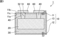
- FIG. 1 is a cross-sectional view schematically showing an example of the electronic component of the present invention.
- FIG. 2 is a cross-sectional view schematically showing an example of an electronic component whose functional part is a capacitor.
- FIG. 3 is an enlarged view of the portion indicated by III in FIG.
- FIG. 4 is an enlarged view of the portion indicated by IV in FIG.
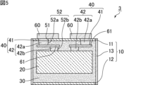
- FIG. 5 is a cross-sectional view schematically showing an example of an electronic component in which the central axis of the first through hole does not coincide with the central axis of the second through hole.
- FIG. 6 is a cross-sectional view schematically showing a first modification of the electronic component shown in FIG.
- FIG. 7 is a cross-sectional view schematically showing a second modification of the electronic component shown in FIG. FIG.
- FIG. 8 is a cross-sectional view schematically showing a modification of the electronic component shown in FIG. 7.
- FIG. 9 is a cross-sectional view schematically showing a modification of the electronic component shown in FIG. 2.
- FIG. 10 is a cross-sectional view schematically showing an electronic component according to an example.
- FIG. 11 is an enlarged view of the portion indicated by XI in FIG.
- the present invention is not limited to the following configuration, and can be modified and applied as appropriate without changing the gist of the present invention.
- the present invention also includes a combination of two or more of the individual preferred configurations of the present invention described below.
- the surface of the filled resin part that seals the functional part is covered with a sealing body.
- the first plate, the lid part, and the sealing metal layer included in the sealing body are made of a material that is less permeable to moisture than the filling resin part, and the sealing metal layer is provided in direct connection with the first plate. By doing so, it is possible to suppress moisture from entering the functional part.
- wiring can be drawn out from the functional section via a via conductor or the like provided inside the through hole penetrating the glass plate and the filled resin section.
- FIG. 1 is a cross-sectional view schematically showing an example of the electronic component of the present invention.
- the electronic component 1 shown in FIG. 1 includes a sealing body 10, a functional section 20, a filled resin section 30, and a via conductor 40.
- the sealing body 10 includes a first plate 11, a lid portion 12, and a sealing metal layer 13.
- the first plate 11 has a first main surface 11a and a second main surface 11b that face each other in the thickness direction, and a side surface 11c that connects the first main surface 11a and the second main surface 11b.
- the lid portion 12 is spaced apart from the first plate 11 so as to face the first main surface 11a of the first plate 11 in the thickness direction.
- the sealing metal layer 13 hermetically seals the internal space of the sealing body 10 together with the first plate 11 and the lid part 12.
- the functional section 20 is provided in the internal space of the sealing body 10 and separated from the first plate 11. In the functional section 20, a potential is applied to a pair of electrodes (not shown).
- the filling resin part 30 is filled between the sealing body 10 and the functional part 20.
- the via conductor 40 is connected to the inside of a first through hole 51 that penetrates the first plate 11 in the thickness direction, and the inside of a second through hole 52 that penetrates the filled resin part 30 in the thickness direction and communicates with the first through hole 51. It is set up at The via conductor 40 is electrically connected to a pair of electrodes of the functional section 20 (for example, a pair of electrodes located on the upper surface side of the functional section 20).
- the central axis of the first through hole 51 coincides with the central axis of the second through hole 52, so the via conductor 40 is provided in a straight line.
- the cross-sectional shape of the first through hole 51 and the second through hole 52 viewed from the thickness direction is not particularly limited, and examples thereof include polygons such as quadrangles, circles, ellipses, and the like.
- the first through hole 51 and the second through hole 52 may have a taper in which the hole diameter becomes smaller in the thickness direction toward the functional part 20.
- the pore diameter refers to the diameter when the cross-sectional shape is circular, and the maximum length passing through the center of the cross-section when the cross-sectional shape is other than circular.
- the via conductors 40 provided inside the first through hole 51 and the second through hole 52 only need to be provided on at least the inner wall surfaces of the first through hole 51 and the second through hole 52.
- the inner wall surfaces of the first through hole 51 and the second through hole 52 are metalized with a low resistance metal such as copper, gold, or silver.
- the metallization of the via conductor 40 is not limited to the case where only the inner wall surfaces of the first through hole 51 and the second through hole 52 are metalized, but metal or a composite material of metal and resin, etc.
- the second through hole 52 may be filled with the second through hole 52.
- the via conductor 40 may be a through-hole conductor that penetrates the sealing body 10 in the thickness direction.
- a through-hole conductor that is not electrically connected to the pair of electrodes of the functional section 20 is provided. Good too. Such a through-hole conductor simply functions as a wiring.
- a through-hole conductor that is not electrically connected to the pair of electrodes of the functional part 20 may be provided so as to penetrate the sealing body 10 in the thickness direction without passing through the functional part 20, and the through-hole conductor may be provided so as to penetrate the sealing body 10 in the thickness direction without passing through the functional part 20. It may be provided so as to penetrate the stopper 10 in the thickness direction. Note that when a through-hole conductor is provided to penetrate the sealing body 10 including the functional part 20 in the thickness direction, an insulating material is filled between the through-hole penetrating the functional part 20 and the through-hole conductor. Ru.
- a wiring 60 electrically connected to the via conductor 40 is provided on the second main surface 11b of the first plate 11.
- the portion of the wiring 60 that is connected to the via conductor 40 may be a land.
- the wiring 60 is mainly composed of a low-resistance metal such as copper, gold, or silver.
- the first plate 11 is a glass plate.
- the water vapor permeability of the lid portion 12 is one-tenth or less when compared to the filled resin portion 30 having the same film thickness.
- Water vapor permeability can be measured, for example, according to JIS K 7129 "Plastics - Films and sheets - How to determine water vapor permeability (gas chromatography method)".
- the water vapor permeability of the lid part 12 should be one-tenth or less of the water vapor permeability of the filled resin part 30.
- the lid part 12 has a water vapor permeability of 1/10 to 1/10 (1/10,000,000,000) or more when compared to, for example, the filled resin part 30 having the same film thickness.
- the lid portion 12 is made of glass or metal, for example.
- the lid part 12 is, for example, a glass plate.
- the glass constituting the lid portion 12 may be the same as or different from the glass constituting the first plate 11.
- a via conductor (which may be a through-hole conductor) may be provided similarly to the first plate 11.
- the via conductor provided in the lid part 12 is connected to the inside of the first through hole that penetrates the lid part 12 in the thickness direction, and the second through hole that penetrates the filled resin part 30 in the thickness direction and communicates with the first through hole. It is provided inside the through hole and electrically connected to a pair of electrodes of the functional section 20 (for example, a pair of electrodes located on the lower surface side of the functional section 20).
- wiring electrically connected to the via conductor be provided on the main surface of the lid portion 12 on the opposite side from the filled resin portion 30.
- the portion of the wiring that is connected to the via conductor may be a land.
- the lid part 12 When the lid part 12 is made of metal, the lid part 12 has the same configuration as the sealing metal layer 13, for example.
- the metal forming the lid portion 12 may be the same as or different from the metal forming the sealing metal layer 13.
- the sealing metal layer 13 is provided in direct connection to the first plate 11. In this case, it is preferable that the sealing metal layer 13 is directly bonded to the first plate 11.
- the sealing metal layer 13 is preferably provided in direct connection with the side surface 11c of the first plate 11. In this case, it is preferable that the sealing metal layer 13 is directly bonded to the side surface 11c of the first plate 11.
- the sealing metal layer 13 is provided in direct connection with the lid part 12. In this case, it is preferable that the sealing metal layer 13 is directly bonded to the lid part 12.
- the sealing metal layer 13 is preferably provided in direct connection with the side surface of the lid portion 12. In this case, it is preferable that the sealing metal layer 13 is directly adhered to the side surface of the lid part 12.
- the sealing metal layer 13 includes, for example, a base layer and a plating layer from the filled resin part 30 side.
- the base layer may be one layer or two or more layers.
- the number of plating layers may be one, or two or more.
- the base layer is formed, for example, by sputtering or electroless plating.
- the base layer includes, for example, an adhesion layer and a power supply layer from the filled resin part 30 side.
- the plating layer is formed by electrolytic plating, for example.
- the filled resin portion 30 is made of resin having insulation properties.
- the resin constituting the filled resin portion 30 include insulating resins such as epoxy resin and phenol resin.
- the filled resin part 30 contains a filler.
- the filler included in the filled resin portion 30 include inorganic fillers such as silica particles, alumina particles, and metal particles.
- the filled resin portion 30 may be composed of only one resin layer, or may be composed of two or more resin layers laminated in the thickness direction.
- the materials constituting each resin layer may be the same or different.
- FIG. 2 is a cross-sectional view schematically showing an example of an electronic component whose functional part is a capacitor.
- the functional section 20 includes an anode plate 21 made of metal.
- the anode plate 21 has a core portion 22 made of valve metal. It is preferable that the anode plate 21 has a porous portion 23 provided on at least one main surface of the core portion 22 .
- a dielectric layer (not shown) is provided on the surface of the porous portion 23, and a cathode layer 24 is provided on the surface of the dielectric layer.
- the functional section 20 forms a capacitor such as a conductive polymer capacitor.
- one via conductor 40 is electrically connected to the core 22 of the anode plate 21, and the other via conductor 40 is electrically connected to the cathode layer 24. Therefore, the core portion 22 of the anode plate 21 and the cathode layer 24 correspond to "a pair of electrodes of the functional section 20.”
- the via conductor 40 may be a through-hole conductor that penetrates the sealing body 10 in the thickness direction.
- a through-hole conductor electrically connected to the core portion 22 of the anode plate 21 is provided so as to penetrate the sealing body 10 including the functional portion 20 in the thickness direction.
- the structure is such that the core portion 22 of the anode plate 21 and the through-hole conductor are directly connected.
- the anode plate 21 is made of a valve metal that exhibits a so-called valve action.
- valve metals include simple metals such as aluminum, tantalum, niobium, titanium, and zirconium, and alloys containing at least one of these metals. Among these, aluminum or aluminum alloy is preferred.
- the shape of the anode plate 21 is preferably flat, and more preferably foil-like.
- the anode plate 21 only needs to have the porous portion 23 on at least one main surface of the core portion 22, and may have the porous portion 23 on both main surfaces of the core portion 22.
- the porous portion 23 is preferably a porous layer formed on the surface of the core portion 22, and more preferably an etched layer.
- the dielectric layer provided on the surface of the porous portion 23 is porous reflecting the surface condition of the porous portion 23, and has a finely uneven surface shape.
- the dielectric layer is preferably made of an oxide film of the valve metal.
- the surface of the aluminum foil is anodized (also referred to as chemical conversion treatment) in an aqueous solution containing ammonium adipate, etc. to form a dielectric layer made of an oxide film. can be formed.
- the cathode layer 24 provided on the surface of the dielectric layer includes, for example, a solid electrolyte layer provided on the surface of the dielectric layer.
- the cathode layer 24 further includes a conductor layer provided on the surface of the solid electrolyte layer.
- the material constituting the solid electrolyte layer examples include conductive polymers such as polypyrroles, polythiophenes, and polyanilines. Among these, polythiophenes are preferred, and poly(3,4-ethylenedioxythiophene) called PEDOT is particularly preferred. Further, the conductive polymer may contain a dopant such as polystyrene sulfonic acid (PSS). Note that the solid electrolyte layer preferably includes an inner layer that fills the pores (recesses) of the dielectric layer and an outer layer that covers the dielectric layer.
- conductive polymers such as polypyrroles, polythiophenes, and polyanilines. Among these, polythiophenes are preferred, and poly(3,4-ethylenedioxythiophene) called PEDOT is particularly preferred.
- the conductive polymer may contain a dopant such as polystyrene sulfonic acid (PSS).
- PSS polystyrene sulfonic acid
- the conductor layer includes at least one of a conductive resin layer and a metal layer.
- the conductor layer may be only a conductive resin layer or only a metal layer.
- the conductor layer preferably covers the entire surface of the solid electrolyte layer.
- the conductive resin layer examples include a conductive adhesive layer containing at least one conductive filler selected from the group consisting of silver filler, copper filler, nickel filler, and carbon filler.
- the metal layer examples include metal plating films, metal foils, and the like.
- the metal layer is preferably made of at least one metal selected from the group consisting of nickel, copper, silver, and alloys containing these metals as main components. Note that the term "main component" refers to an elemental component having the largest elemental weight ratio.
- the conductor layer includes, for example, a carbon layer provided on the surface of the solid electrolyte layer and a copper layer provided on the surface of the carbon layer.
- the carbon layer is provided to electrically and mechanically connect the solid electrolyte layer and the copper layer.
- the carbon layer can be formed in a predetermined area by applying carbon paste onto the solid electrolyte layer by a method such as sponge transfer, screen printing, dispenser coating, or inkjet printing.
- the copper layer can be formed in a predetermined area by applying a copper paste onto the carbon layer by a method such as sponge transfer, screen printing, spray coating, dispenser coating, or inkjet printing.
- the functional unit 20 is a capacitor
- a ceramic capacitor using barium titanate or a thin film capacitor using silicon nitride (SiN), silicon dioxide (SiO 2 ), hydrogen fluoride (HF), etc. is used as the capacitor. It is also possible.
- the functional part 20 is a capacitor based on a metal such as aluminum. A conductive polymer capacitor whose base material is a metal such as aluminum is more preferable.
- Examples of the functional unit 20 that requires moisture resistance include capacitors such as conductive polymer capacitors and high dielectric constant thin film capacitors, batteries such as all-solid-state batteries, and lithium ion secondary batteries (LIBs).
- capacitors such as conductive polymer capacitors and high dielectric constant thin film capacitors
- batteries such as all-solid-state batteries
- LIBs lithium ion secondary batteries
- FIG. 3 is an enlarged view of the portion indicated by III in FIG. 1.
- a first adhesive layer 14 is provided between the filled resin part 30 and the first plate 11.
- the first adhesive layer 14 can improve the adhesion between the filled resin part 30 and the first plate 11.
- the first adhesive layer 14 has insulation and adhesive properties.
- the first adhesive layer 14 is made of, for example, an epoxy adhesive sheet, an epoxy adhesive, an acrylic adhesive sheet, an acrylic adhesive, or the like.
- the first adhesive layer 14 may be provided on the entire surface between the filled resin portion 30 and the first plate 11, or may be provided on a portion thereof.
- the Young's modulus of the first adhesive layer 14 is preferably lower than the Young's modulus of the first plate 11 and lower than the Young's modulus of the filled resin portion 30. In this case, when the filled resin portion 30 thermally expands, the first adhesive layer 14 can absorb the thermal expansion of the filled resin portion 30.
- the Young's modulus of the first adhesive layer 14 is, for example, 0.005 GPa or more and 2.9 GPa or less.
- the Young's modulus of the first plate 11 is, for example, 50 GPa or more and 90 GPa or less.
- the Young's modulus of the filled resin portion 30 is, for example, 3 GPa or more and 50 GPa or less.
- Young's modulus can be measured, for example, by a static test method (bending test).
- the thickness of the first plate 11 is preferably 200 ⁇ m or less. In this case, thermal expansion of the filled resin portion 30 can be allowed by deformation of the first plate 11.
- the thickness of the first plate 11 is preferably 5 ⁇ m or more from the viewpoint of ensuring the mechanical strength of the first plate 11.
- the thickness of the first plate 11 means the dimension of the first plate 11 in the thickness direction of the first plate 11.
- the thickness of the sealing metal layer 13 is preferably four times or less the thickness of the first plate 11, and more preferably thinner than the thickness of the first plate 11. preferable. In this case, thermal expansion of the filled resin portion 30 can be tolerated by deforming both the first plate 11 and the sealing metal layer 13.
- the thickness of the sealing metal layer 13 is preferably 10 ⁇ m or more from the viewpoint of suppressing moisture from entering the functional section 20.
- the thickness of the sealing metal layer 13 means the dimension of the sealing metal layer 13 in a direction parallel to the main surface of the first plate 11.
- the lid portion 12 is plate-shaped, and the thickness of the lid portion 12 is preferably 200 ⁇ m or less. In this case, the thermal expansion of the filled resin part 30 can also be allowed by deformation of the lid part 12.
- the thickness of the lid part 12 is preferably 5 ⁇ m or more from the viewpoint of ensuring the mechanical strength of the lid part 12. Note that the thickness of the lid portion 12 may be the same as or different from the thickness of the first plate 11.
- the thickness of the lid 12 means the dimension of the lid 12 in the thickness direction of the first plate 11.
- FIG. 4 is an enlarged view of the portion indicated by IV in FIG. 1.
- the second adhesive layer 15 is provided between the filled resin part 30 and the lid part 12, as shown in FIG.
- the adhesion between the filled resin part 30 and the lid part 12 can be improved by the second adhesive layer 15.
- the second adhesive layer 15 has insulation and adhesive properties.
- the second adhesive layer 15 is made of, for example, an epoxy adhesive sheet, an epoxy adhesive, an acrylic adhesive sheet, an acrylic adhesive, or the like.
- the second adhesive layer 15 may be provided on the entire surface between the filled resin portion 30 and the lid portion 12, or may be provided on a portion thereof.
- the material of the second adhesive layer 15 may be the same as or different from the material of the first adhesive layer 14.
- the Young's modulus of the second adhesive layer 15 is preferably lower than the Young's modulus of the lid portion 12 and lower than the Young's modulus of the filled resin portion 30. In this case, when the filled resin portion 30 thermally expands, the second adhesive layer 15 can absorb the thermal expansion of the filled resin portion 30.
- the Young's modulus of the second adhesive layer 15 is, for example, 0.005 GPa or more and 2.9 GPa or less.
- the Young's modulus of the second adhesive layer 15 may be the same as or different from the Young's modulus of the first adhesive layer 14.
- the Young's modulus of the lid part 12 is, for example, 50 GPa or more and 90 GPa or less.
- the Young's modulus of the lid 12 may be the same as or different from the Young's modulus of the first plate 11.
- FIG. 5 is a cross-sectional view schematically showing an example of an electronic component in which the central axis of the first through hole does not coincide with the central axis of the second through hole.
- the central axis of the first through hole 51 does not coincide with the central axis of the second through hole 52.
- the second through hole 52 includes a second through hole 52a on the first plate 11 side and a second through hole 52b on the functional part 20 side, and the central axis of the first through hole 51 does not coincide with the central axis of the second through hole 52b on the functional section 20 side.
- the central axis of the second through hole 52a on the first plate 11 side does not match the central axis of the second through hole 52b on the functional part 20 side.
- the central axis of the first through hole 51 may coincide with the central axis of the second through hole 52a on the first plate 11 side, or may coincide with the central axis of the second through hole 52a on the first plate 11 side. You don't have to.
- the via conductor 40 includes a first via conductor 41 provided inside the first through hole 51 and a second via conductor 42 provided inside the second through hole 52.
- the central axis of the first via conductor 41 is located on the side of the central axis of the second via conductor 42.
- the first via conductor 41 and the second via conductor 42 are electrically connected by a wiring 61 provided in the filled resin part 30.
- the second via conductor 42 includes a second via conductor 42a provided inside the second through hole 52a on the first plate 11 side, and a second via conductor 42a provided inside the second through hole 52b on the functional part 20 side.
- the center axis of the first via conductor 41 is located on the side of the center axis of the second via conductor 42b on the functional section 20 side.
- the central axis of the second via conductor 42a on the first plate 11 side is located on the side of the central axis of the second via conductor 42b on the functional section 20 side.
- the central axis of the first via conductor 41 may coincide with the central axis of the second via conductor 42a on the first plate 11 side, and is located to the side of the central axis of the second via conductor 42a on the first plate 11 side. You may.
- the via conductor 40 is divided into a first via conductor 41 and a second via conductor 42 so that the first via conductor 41 and the second via conductor 42 are not lined up in a straight line. This makes it possible to alleviate the stress applied to the first plate 11 when the via conductor 40 thermally expands in the thickness direction.
- the first via conductor 41 does not overlap with the second via conductor 42 when viewed from the thickness direction.
- the first via conductor 41 does not overlap the second via conductor 42b on the functional section 20 side when viewed from the thickness direction.
- the first via conductor 41 may or may not overlap the second via conductor 42a on the first plate 11 side.
- the second via conductor 42a on the first plate 11 side may or may not overlap with the second via conductor 42b on the functional section 20 side.
- the wiring 61 only needs to be placed between the first plate 11 and the functional section 20.
- the wiring 61 is arranged apart from the first plate 11 and the functional section 20, but the wiring 61 may be arranged so as to be in contact with the first plate 11, for example.
- the second via conductor 42 does not include the second via conductor 42a on the first plate 11 side, but only the second via conductor 42b on the functional part 20 side. include.
- the wiring 61 between the first via conductor 41 and the second via conductor 42 is mainly composed of a low-resistance metal such as copper, gold, or silver.
- the material of the wiring 61 may be the same as or different from the material of the wiring 60.
- the thickness of the wiring 61 is preferably 0.5 ⁇ m or more and 40 ⁇ m or less.
- the electronic component 2 shown in FIG. 2 As in the electronic component 1 shown in FIG. 1, the electronic component 2 shown in FIG. 2, and the electronic component 3 shown in FIG. It is preferable that it is provided only in the area between. Furthermore, it is preferable that the first through hole 51 is provided only in a region overlapping with the functional section 20 when viewed from the thickness direction. In this case, since the electronic components 1, 2, and 3 do not spread in the width direction, miniaturization is possible.
- the thickness is preferably thinner than 20 mm. Furthermore, in the filled resin part 30, the thickness between the lid part 12 and the functional part 20 is preferably thinner than the thickness of the functional part 20. In this case, since the electronic components 1, 2, and 3 do not spread in the thickness direction, miniaturization is possible.
- the flatness of the second main surface 11b of the plate 11 is preferably 30 nm or less in terms of arithmetic mean roughness. Since the first plate 11 is a glass plate, its flatness is high. Therefore, fine wiring 60 can be formed.
- the flatness of the second main surface 11b of the first plate 11 is preferably 0.1 nm or more in terms of arithmetic mean roughness.
- arithmetic mean roughness is the surface roughness measured based on JIS B 0601:2013.
- FIG. 6 is a cross-sectional view schematically showing a first modification of the electronic component shown in FIG. 1.
- the sealing metal layer 13 may be provided from the side surface 11c of the first plate 11 to the second main surface 11b of the first plate 11.
- the connection area of the sealing metal layer 13 is increased by connecting the sealing metal layer 13 not only to the side surface 11c of the first plate 11 but also to the second main surface 11b of the first plate 11. Therefore, thermal expansion of the filled resin portion 30 can be allowed.
- the sealing metal layer 13 may be provided from the side surface of the lid part 12 to the main surface of the lid part 12 opposite to the filled resin part 30.
- FIG. 7 is a cross-sectional view schematically showing a second modification of the electronic component shown in FIG. 1.
- an outer resin portion 31 may be provided on the second main surface 11b of the first plate 11.
- the outer resin portion 31 is made of a resin having insulation properties, similar to the filled resin portion 30.
- the outer resin portion 31 may be made of the same material as the filled resin portion 30, or may be made of a different material.
- the outer resin portion 31 may be composed of only one resin layer, or may be composed of two or more resin layers laminated in the thickness direction. When the outer resin portion 31 is composed of two or more resin layers, the materials constituting each resin layer may be the same or different.
- the thickness of the outer resin part 31 is preferably thinner than the thickness of the filled resin part 30 between the first plate 11 and the functional part 20. In this case, since the electronic component 5 does not spread in the thickness direction, miniaturization is possible.
- the surface roughness of the surface opposite to the surface in contact with the first plate 11 is preferably greater than the surface roughness of the surface in contact with the first plate 11.
- the electronic component 5 is embedded, for example, inside a board of an HPC (high performance computer) or the like. Therefore, by increasing the surface roughness of the outer surface of the outer resin part 31, the adhesion between the outer resin part 31 and the substrate can be improved.
- the surface roughness of the surface opposite to the surface in contact with the first plate 11 is preferably 300 nm or more and 3000 nm or less in terms of arithmetic mean roughness.
- a wiring 60 electrically connected to the via conductor 40 is provided on the surface of the outer resin portion 31 opposite to the surface in contact with the first plate 11.
- the portion of the wiring 60 that is connected to the via conductor 40 may be a land.
- the wiring 60 is provided on the surface of the outer resin part 31 opposite to the surface in contact with the first plate 11
- the wiring 60 is provided on the surface of the outer resin part 31 opposite to the surface in contact with the first plate 11.
- the surface roughness of the surface not provided with may be greater than the surface roughness of the surface in contact with the wiring 60.
- the via conductor 40 is connected to the inside of the first through hole 51 that penetrates the first plate 11 in the thickness direction, and to the filled resin portion. 30 in the thickness direction and communicates with the first through hole 51; and a third through hole 53 that penetrates the outer resin part 31 in the thickness direction and communicates with the first through hole 51. It is provided inside and electrically connected to a pair of electrodes of the functional section 20 (for example, a pair of electrodes located on the upper surface side of the functional section 20).
- the central axis of the first through hole 51 coincides with the central axis of the second through hole 52, and the central axis of the second through hole 52 coincides with the central axis of the third through hole 53. Therefore, the via conductor 40 is provided in a straight line.
- the central axis of the first through hole 51 does not have to coincide with the central axis of the second through hole 52, and the central axis of the second through hole 52 is the center of the third through hole 53. It doesn't have to match the axis.
- the via conductors provided inside the through holes whose central axes do not coincide are electrically connected by wiring 61 provided in the filled resin portion 30 (see FIG. 5).
- wiring 61 provided in the filled resin portion 30 (see FIG. 5).
- the second through hole 52 is preferably provided only in the region between the first plate 11 and the functional section 20 in the filled resin section 30. Furthermore, it is preferable that at least one of the first through hole 51 and the third through hole 53 is provided only in a region overlapping with the functional part 20 when viewed from the thickness direction, and the first through hole 51 and the third through hole It is more preferable that both of 53 are provided only in the region overlapping with the functional section 20 when viewed from the thickness direction. In this case, since the electronic component 5 does not spread in the width direction, miniaturization is possible.
- an adhesive layer is provided between the filled resin part 30 and the first plate 11, as in FIG. Preferably, an adhesive layer is provided between them.
- an outer resin portion 31 may be provided on the main surface of the lid portion 12 on the opposite side from the filled resin portion 30.
- the outer resin portion 31 provided on the main surface opposite to the filling resin portion 30 of the lid portion 12 may be made of the same material as the outer resin portion 31 provided on the second main surface 11b of the first plate 11. It may well be constructed from different materials.
- the outer resin part 31 provided on the main surface of the lid part 12 on the opposite side to the filled resin part 30 may be composed of only one resin layer, or may be composed of two or more resin layers laminated in the thickness direction. may be configured.
- the materials constituting each resin layer may be the same or different.
- the thickness of the outer resin part 31 provided on the main surface of the lid part 12 opposite to the filled resin part 30 is thinner than the thickness of the filled resin part 30 between the lid part 12 and the functional part 20. In this case, since the electronic component 5 does not spread in the thickness direction, miniaturization is possible.
- the thickness of the outer resin part 31 provided on the main surface opposite to the filled resin part 30 of the lid part 12 may be the same as the thickness of the outer resin part 31 provided on the second main surface 11b of the first plate 11, May be different.
- the surface roughness of the surface opposite to the surface in contact with the lid part 12 is greater than the surface roughness of the surface in contact with the lid part 12. It is preferable that it is also large.
- the surface roughness of the outer resin portion 31 provided on the main surface opposite to the filled resin portion 30 of the lid portion 12 is the same as the surface roughness of the outer resin portion 31 provided on the second main surface 11b of the first plate 11. However, it may be different.
- the surface roughness of the surface opposite to the surface in contact with the lid portion 12 is preferably 300 nm or more and 3000 nm or less in terms of arithmetic mean roughness.
- a via conductor may be provided similarly to the first plate 11.
- the via conductor provided in the lid part 12 is connected to the inside of the first through hole that penetrates the lid part 12 in the thickness direction, and the second through hole that penetrates the filled resin part 30 in the thickness direction and communicates with the first through hole.
- the pair of electrodes of the functional part 20 (for example, the bottom surface of the functional part 20 a pair of electrodes located on the sides).
- wiring is preferably provided on the surface opposite to the surface in contact with the lid portion 12.
- the portion of the wiring that is connected to the via conductor may be a land.
- the lid of the outer resin part 31 On the surface opposite to the surface in contact with the portion 12, the surface roughness of the surface on which no wiring is provided may be greater than the surface roughness of the surface in contact with the wiring.
- an adhesive layer is provided between the filled resin part 30 and the lid part 12, as in FIG. 4, and between the outer resin part 31 and the lid part 12. It is preferable that an adhesive layer is provided on.
- FIG. 8 is a sectional view schematically showing a modification of the electronic component shown in FIG. 7.
- the sealing metal layer 13 is provided from the side surface 11c of the first plate 11 to the surface of the outer resin part 31 opposite to the surface in contact with the first plate 11. Good too.
- the sealing metal layer 13 contacts the lid portion 12 in the outer resin portion 31 from the side surface of the lid portion 12. It may also be provided on the opposite side.
- FIG. 9 is a cross-sectional view schematically showing a modification of the electronic component shown in FIG. 2.
- the functional section 20 When the functional section 20 is a capacitor like the electronic component 7 shown in FIG. 9, the functional section 20 may include a plurality of capacitor elements 25.
- the plurality of capacitor elements 25 are arranged so as to be lined up on a plane, but they may be arranged so as to be stacked in the thickness direction, or they may be arranged in a combination of both.
- the functional section 20 includes a plurality of capacitor elements 25, a region including the plurality of capacitor elements 25 corresponds to the functional section 20. Therefore, even if the second through hole 52 is provided between the capacitor elements 25 stacked in the thickness direction, the location where the second through hole 52 is provided is between the first plate 11 and the functional part. It corresponds to "between 20".
- the number of capacitor elements 25 is not particularly limited as long as it is two or more.
- the size, shape, etc. of the capacitor elements 25 may be the same, or may be partially or completely different.
- the configurations of the capacitor elements 25 are preferably the same, but capacitor elements 25 with different configurations may be included.
- FIG. 10 is a cross-sectional view schematically showing an electronic component according to an example.
- FIG. 11 is an enlarged view of the portion indicated by XI in FIG.
- the functional part 20 includes an anode plate 21 in which porous parts 23 are provided on both main surfaces of a core part 22 made of a valve metal, and a dielectric layer (not shown) provided on the surface of the porous part 23. and a cathode layer 24 provided on the surface of the dielectric layer.
- the core portion 22 of the anode plate 21 and the cathode layer 24 correspond to "a pair of electrodes of the functional section 20.”
- the filled resin part 30 is formed by laminating a build-up film (for example, ABF (Ajinomoto Build-up Film), etc.) on both the front and back sides of the functional part 20 and performing a curing process.
- a build-up film for example, ABF (Ajinomoto Build-up Film), etc.
- two glass plates for example, G-Leaf (registered trademark) (manufactured by Nippon Electric Glass Co., Ltd., thickness 50 ⁇ m), etc.) are prepared as the first plate 11 and the lid part 12.
- an adhesive layer 14a for example, a double-sided adhesive sheet, etc.
- an adhesive layer for example, a double-sided adhesive sheet, etc.
- a build-up film for example, ABF (Ajinomoto Build-up Film), etc. is attached to the adhesive layer, and a curing process is performed. As a result, the outer resin portion 31 is formed.
- a through hole extending from the surface of the outer resin part 31 to the functional part 20 is formed by two-step processing using a femtosecond green laser and a CO 2 laser. Specifically, a through hole is formed from the surface of the outer resin part 31 to the first plate 11 or the lid part 12 using a femtosecond green laser, and a through hole is formed from the first plate 11 or the lid part 12 to the functional part 20 using CO2. 2. A through hole is formed using a laser.
- Electrodes are patterned by electroless plating, photolithography, electrolytic plating, resist peeling, electroless plating and etching. As a result, via conductors 40 and wiring 60 are formed.
- the front and back surfaces of the outer resin portion 31 are covered with a thermal release sheet.
- a base layer for the sealing metal layer 13 is formed on the side surface of the laminate.
- a power supply layer (Cu) with a thickness of 1000 nm is formed.
- the power supply layer (Cu) with a thickness of 1000 nm may be formed by electroless plating instead of sputtering.
- the thermal release sheet is peeled off from the laminate on which the base layer of the sealing metal layer 13 is formed.
- a plating layer of the sealing metal layer 13 is formed on the side surface of the laminate from which the thermal release sheet has been peeled off.
- Cu: 20 ⁇ m thick/Ni: 5 ⁇ m thick plating layer Cu: 20 ⁇ m thick/Ni: 5 ⁇ m thick/Au: 1 ⁇ m thick plating layer, or Cu: 20 ⁇ m thick/Ni: thickness 5 ⁇ m/Sn: Form a plating layer with a thickness of 2 ⁇ m.
- a through hole penetrating the laminate can be formed using a UV laser instead of the two-step processing using a femtosecond green laser and a CO 2 laser. I can do it.
- the electronic component of the present invention is not limited to the above embodiments, and various applications and modifications can be made within the scope of the present invention regarding the configuration of the electronic component, manufacturing conditions of the electronic component, etc. .
- sealing body 11 first plate 11a first main surface of first plate 11b second main surface of first plate 11c of first plate Side surface 12 Lid part 13 Sealing metal layer 14 First adhesive layer 14a, 14b Adhesive layer 15 Second adhesive layer 20 Functional part 21 Anode plate 22 Core part 23 Porous part 24 Cathode layer 25 Capacitor element 30 Filled resin part 31 Outer resin Part 40 Via conductor 41 First via conductor 42, 42a, 42b Second via conductor 51 First through hole 52, 52a, 52b Second through hole 53 Third through hole 60, 61 Wiring
Abstract
This electronic component 1 comprises: a sealing body 10 including a first plate 11 having a first main surface 11a and a second main surface 11b that face each other in the thickness direction, and a side plate 11c connecting the first main surface 11a and the second main surface 11b, a lid part 12 disposed separated from the first plate 11 so as to face the first main surface 11a of the first plate 11 in the thickness direction, and a sealing metal layer 13 that hermetically seals an internal space together with the first plate 11 and the lid part 12; a functional unit 20 which is provided separated from the first plate 11 in the internal space of the sealing body 10, and in which a potential is applied to a pair of electrodes; a filled resin part 30 filled between the sealing body 10 and the functional unit 20; and a via conductor 40 that is provided inside of a first through-hole 51 penetrating the first plate 11 in the thickness direction, and inside of a second through-hole 52 penetrating the filled resin part 30 in the thickness direction and communicating with the first through-hole 51, the via conductor being electrically connected to the pair of electrodes of the functional unit 20. The lid part 12 has at most 1/10th the water vapor permeability of the filled resin part 30 of the same thickness, or the lid part 12 is formed from glass or metal. The first plate 11 is a glass plate. The sealing metal layer 13 is provided directly connected to the first plate 11.
Description
本発明は、電子部品に関する。
The present invention relates to electronic components.
湿度に弱い機能部を有する電子部品においては、使用環境下の水分から機能部を保護するため、樹脂、金属又はガラス等の材料を用いて機能部が封止される。
In electronic components that have functional parts that are sensitive to humidity, the functional parts are sealed using materials such as resin, metal, or glass in order to protect the functional parts from moisture in the usage environment.
特許文献1には、支持体要素(3)と、支持体要素(3)の上に取り付けられた少なくとも1つのオプトエレクトロニクス素子(2)と、オプトエレクトロニクス素子(2)のためのカバー(5)と、キャビティ(11)と、を有するオプトエレクトロニクスモジュール(1)が開示されている。カバー(5)は、オプトエレクトロニクス素子(2)を周方向で完全に取り囲んでいて、かつ、支持体要素(3)に結合されているフレーム(7)と、電磁放射をカバー(5)内に入射させるため、かつ/または、カバー(5)から出射させるための、フレーム(7)に取り付けられていて、かつ、支持体要素(3)に実質的に対向して位置するガラス要素(9,90)と、を有する。キャビティ(11)は、少なくとも部分的にカバー(5)の内面と支持体要素(3)の面とによって画定された容積の内部に形成されている。オプトエレクトロニクス素子(2)は、カバー(5)によって気密にかつ/またはオートクレーブ可能に封入されるように、キャビティ(11)内に配置されている。オプトエレクトロニクスモジュール(1)は、キャビティ(11)を少なくとも部分的に充填している充填材料(13)を有する。オプトエレクトロニクスモジュール(1)は、充填材料(13)が占める体積の膨張を補償するように構成および形成されており、このために、変形可能な少なくとも1つの第1の補償容積(15)を有する。
WO 2006/000001 discloses a carrier element (3), at least one optoelectronic element (2) mounted on the carrier element (3) and a cover (5) for the optoelectronic element (2). An optoelectronic module (1) is disclosed having: a cavity (11); The cover (5) has a frame (7) which completely surrounds the optoelectronic element (2) in the circumferential direction and which is connected to the support element (3) and which directs electromagnetic radiation into the cover (5). A glass element (9, 90). The cavity (11) is formed inside a volume defined at least partially by the inner surface of the cover (5) and the surface of the support element (3). The optoelectronic component (2) is arranged in the cavity (11) in such a way that it is hermetically and/or autoclavably enclosed by the cover (5). The optoelectronic module (1) has a filling material (13) that at least partially fills the cavity (11). The optoelectronic module (1) is configured and formed to compensate for the expansion of the volume occupied by the filling material (13) and has for this purpose at least one first compensating volume (15) which is deformable. .
特許文献1には、オプトエレクトロニクス素子(2)を気密にかつ/またはオートクレーブ可能に封入するために、カバー(5)を支持体要素(3)に結合することは、以下のプロセスのうちの1つによって実施されること、すなわち、
・レーザ溶接、この場合、支持体要素(3)は、好ましくはセラミックまたは金属であり、フレーム(7)は、好ましくはセラミックまたは金属、とりわけガラスによってコーティングされた金属であり、
・抵抗溶接、
・金属はんだを用いたはんだ付け、この場合、支持体要素(3)およびカバー(5)は、それぞれ、はんだとの堅固な結合を確立するために適した表面、好ましくははんだプリフォームを有する表面を有し、
・ガラスはんだを用いたはんだ付け、
・充填材料(13)を用いた、少なくともフレーム(7)とガラス要素(9)との接着、フレーム(7)と支持体要素(3)との接着、またはガラス要素(9)と支持体要素(3)との接着、
・充填材料(13)とは異なるシリコーン、ポリマーまたは接合材料を用いた、少なくともフレーム(7)とガラス要素(9)との接着、フレーム(7)と支持体要素(3)との接着、またはガラス要素(9)と支持体要素(3)との接着
のうちの1つによって実施されることが記載されている。 WO 2006/000001 discloses that bonding the cover (5) to the support element (3) in order to hermetically and/or autoclavably encapsulate the optoelectronic element (2) can be carried out by one of the following processes: to be carried out by one person, i.e.
- laser welding, in which case the support element (3) is preferably ceramic or metal, the frame (7) is preferably ceramic or metal, in particular metal coated with glass;
・Resistance welding,
- soldering with metal solder, in which case the support element (3) and the cover (5) each have a surface suitable for establishing a firm bond with the solder, preferably a surface with a solder preform has
・Soldering using glass solder,
adhesion of at least the frame (7) and the glass element (9), the adhesion of the frame (7) and the support element (3), or the glass element (9) and the support element, using a filler material (13); (3) Adhesion with
adhesion of at least the frame (7) and the glass element (9), the adhesion of the frame (7) and the support element (3) with a silicone, polymer or bonding material different from the filler material (13); or It is stated that this is carried out by one of gluing the glass element (9) and the support element (3).
しかしながら、特許文献1に記載されたオプトエレクトロニクスモジュール(1)においては、フレーム(7)とガラス要素(9)との間、又は、フレーム(7)と支持体要素(3)との間から水分が浸入するおそれがある。
However, in the optoelectronic module (1) described in Patent Document 1, moisture is removed between the frame (7) and the glass element (9) or between the frame (7) and the support element (3). There is a risk of infiltration.
特に、湿度に弱い機能部を有する電子部品においては、浸入した水分が機能部に到達した場合、浸入した水分によって機能の損失又は劣化が生じてしまう。
In particular, in electronic components that have functional parts that are sensitive to humidity, if the infiltrated moisture reaches the functional parts, the infiltrated moisture will cause loss or deterioration of the function.
本発明は、上記の問題を解決するためになされたものであり、機能部への水分の浸入を抑制できる電子部品を提供することを目的とする。
The present invention has been made in order to solve the above problems, and an object of the present invention is to provide an electronic component that can suppress the infiltration of moisture into functional parts.
本発明の電子部品は、厚み方向に相対する第1の主面及び第2の主面と、上記第1の主面及び上記第2の主面をつなぐ側面とを有する第1板と、上記厚み方向において上記第1板の上記第1の主面に対向するように上記第1板から離隔して配置された蓋部と、上記第1板及び上記蓋部とともに内部空間を気密に封止する封止金属層と、を含む封止体と、上記封止体の内部空間に上記第1板から離隔して設けられ、一対の電極に電位が印加される機能部と、上記封止体と上記機能部との間に充填された充填樹脂部と、上記第1板を上記厚み方向に貫通する第1貫通孔の内部と、上記充填樹脂部を上記厚み方向に貫通し、上記第1貫通孔に連通する第2貫通孔の内部とに設けられ、上記機能部の上記一対の電極に電気的に接続されたビア導体と、を備える。上記蓋部は、同一膜厚の上記充填樹脂部と比較したときに水蒸気透過度が10分の1以下であるか、あるいは、上記蓋部は、ガラス又は金属から構成される。上記第1板は、ガラス板である。上記封止金属層は、上記第1板に直接接続して設けられている。
The electronic component of the present invention includes a first plate having a first main surface and a second main surface facing each other in the thickness direction, and a side surface connecting the first main surface and the second main surface; a lid portion disposed apart from the first plate so as to face the first principal surface of the first plate in the thickness direction; and an internal space hermetically sealed together with the first plate and the lid portion. a sealing body including: a sealing metal layer; a functional section provided in an internal space of the sealing body spaced apart from the first plate; and a functional section to which a potential is applied to a pair of electrodes; and the functional section; a first through-hole passing through the first plate in the thickness direction; a via conductor provided inside the second through hole communicating with the through hole and electrically connected to the pair of electrodes of the functional section. The lid portion has a water vapor permeability of 1/10 or less when compared to the filled resin portion having the same film thickness, or the lid portion is made of glass or metal. The first plate is a glass plate. The sealing metal layer is provided in direct connection with the first plate.
本発明によれば、機能部への水分の浸入を抑制できる電子部品を提供することができる。
According to the present invention, it is possible to provide an electronic component that can suppress moisture from entering the functional part.
以下、本発明の電子部品について説明する。
しかしながら、本発明は、以下の構成に限定されるものではなく、本発明の要旨を変更しない範囲において適宜変更して適用することができる。なお、以下において記載する本発明の個々の好ましい構成を2つ以上組み合わせたものもまた本発明である。 Hereinafter, the electronic component of the present invention will be explained.
However, the present invention is not limited to the following configuration, and can be modified and applied as appropriate without changing the gist of the present invention. Note that the present invention also includes a combination of two or more of the individual preferred configurations of the present invention described below.
本発明の電子部品では、機能部を封止する充填樹脂部の表面が封止体で覆われている。封止体に含まれる第1板、蓋部及び封止金属層が充填樹脂部に比べて水分を透過しにくい材料から構成されるとともに、封止金属層が第1板に直接接続して設けられることにより、機能部への水分の浸入を抑制することができる。
In the electronic component of the present invention, the surface of the filled resin part that seals the functional part is covered with a sealing body. The first plate, the lid part, and the sealing metal layer included in the sealing body are made of a material that is less permeable to moisture than the filling resin part, and the sealing metal layer is provided in direct connection with the first plate. By doing so, it is possible to suppress moisture from entering the functional part.
なお、充填樹脂部の表面の全体がガラス材料で覆われることでも、機能部への水分の浸入を抑制することは可能である。しかし、ガラス材料の線膨張係数は樹脂材料の線膨張係数に比べて小さいため、高温時に充填樹脂部が膨張した際、熱応力によって封止構造が破壊されるおそれがある。これに対し、本発明の電子部品では、充填樹脂部の表面の一部が封止金属層で覆われているため、充填樹脂部が熱膨張した際、封止金属層も熱膨張することによって熱応力を緩和することができる。
Note that it is also possible to suppress the infiltration of moisture into the functional part by covering the entire surface of the filled resin part with a glass material. However, since the coefficient of linear expansion of the glass material is smaller than that of the resin material, when the filled resin portion expands at high temperatures, the sealing structure may be destroyed by thermal stress. In contrast, in the electronic component of the present invention, a part of the surface of the filled resin part is covered with the sealing metal layer, so when the filled resin part thermally expands, the sealing metal layer also thermally expands. Thermal stress can be alleviated.
さらに、本発明の電子部品では、ガラス板及び充填樹脂部を貫通する貫通孔の内部に設けられたビア導体等を介して、機能部から外部に配線を引き出すことができる。
Furthermore, in the electronic component of the present invention, wiring can be drawn out from the functional section via a via conductor or the like provided inside the through hole penetrating the glass plate and the filled resin section.
以下に示す図面は模式図であり、その寸法、縦横比の縮尺等は実際の製品と異なる場合がある。
The drawings shown below are schematic diagrams, and their dimensions, aspect ratios, etc. may differ from the actual product.
図1は、本発明の電子部品の一例を模式的に示す断面図である。
FIG. 1 is a cross-sectional view schematically showing an example of the electronic component of the present invention.
図1に示す電子部品1は、封止体10と、機能部20と、充填樹脂部30と、ビア導体40と、を備える。
The electronic component 1 shown in FIG. 1 includes a sealing body 10, a functional section 20, a filled resin section 30, and a via conductor 40.
封止体10は、第1板11と、蓋部12と、封止金属層13と、を含む。
The sealing body 10 includes a first plate 11, a lid portion 12, and a sealing metal layer 13.
第1板11は、厚み方向に相対する第1の主面11a及び第2の主面11bと、第1の主面11a及び第2の主面11bをつなぐ側面11cとを有する。
The first plate 11 has a first main surface 11a and a second main surface 11b that face each other in the thickness direction, and a side surface 11c that connects the first main surface 11a and the second main surface 11b.
蓋部12は、厚み方向において第1板11の第1の主面11aに対向するように第1板11から離隔して配置されている。
The lid portion 12 is spaced apart from the first plate 11 so as to face the first main surface 11a of the first plate 11 in the thickness direction.
封止金属層13は、第1板11及び蓋部12とともに封止体10の内部空間を気密に封止する。
The sealing metal layer 13 hermetically seals the internal space of the sealing body 10 together with the first plate 11 and the lid part 12.
機能部20は、封止体10の内部空間に第1板11から離隔して設けられている。機能部20では、一対の電極(図示せず)に電位が印加される。
The functional section 20 is provided in the internal space of the sealing body 10 and separated from the first plate 11. In the functional section 20, a potential is applied to a pair of electrodes (not shown).
充填樹脂部30は、封止体10と機能部20との間に充填されている。
The filling resin part 30 is filled between the sealing body 10 and the functional part 20.
ビア導体40は、第1板11を厚み方向に貫通する第1貫通孔51の内部と、充填樹脂部30を厚み方向に貫通し、第1貫通孔51に連通する第2貫通孔52の内部とに設けられている。ビア導体40は、機能部20の一対の電極(例えば、機能部20の上面側に位置する一対の電極)に電気的に接続されている。
The via conductor 40 is connected to the inside of a first through hole 51 that penetrates the first plate 11 in the thickness direction, and the inside of a second through hole 52 that penetrates the filled resin part 30 in the thickness direction and communicates with the first through hole 51. It is set up at The via conductor 40 is electrically connected to a pair of electrodes of the functional section 20 (for example, a pair of electrodes located on the upper surface side of the functional section 20).
図1に示す例では、第1貫通孔51の中心軸が第2貫通孔52の中心軸と一致しているため、ビア導体40が直線状に設けられている。
In the example shown in FIG. 1, the central axis of the first through hole 51 coincides with the central axis of the second through hole 52, so the via conductor 40 is provided in a straight line.
厚み方向から見た第1貫通孔51及び第2貫通孔52の断面形状は特に限定されず、例えば、四角形等の多角形、円形、楕円形等が挙げられる。第1貫通孔51及び第2貫通孔52は、機能部20に向かって厚み方向に孔径が小さくなるテーパーを有してもよい。なお、孔径とは、断面形状が円形の場合には直径、円形以外の場合には断面の中心を通る最大長さをいう。
The cross-sectional shape of the first through hole 51 and the second through hole 52 viewed from the thickness direction is not particularly limited, and examples thereof include polygons such as quadrangles, circles, ellipses, and the like. The first through hole 51 and the second through hole 52 may have a taper in which the hole diameter becomes smaller in the thickness direction toward the functional part 20. Note that the pore diameter refers to the diameter when the cross-sectional shape is circular, and the maximum length passing through the center of the cross-section when the cross-sectional shape is other than circular.
第1貫通孔51の内部と第2貫通孔52の内部とに設けられるビア導体40は、第1貫通孔51及び第2貫通孔52の少なくとも内壁面に設けられていればよい。第1貫通孔51及び第2貫通孔52の内壁面は、銅、金又は銀等の低抵抗の金属によってメタライズされる。なお、ビア導体40のメタライズについては、第1貫通孔51及び第2貫通孔52の内壁面のみをメタライズする場合に限られず、金属あるいは金属と樹脂との複合材料等を第1貫通孔51及び第2貫通孔52に充填してもよい。
The via conductors 40 provided inside the first through hole 51 and the second through hole 52 only need to be provided on at least the inner wall surfaces of the first through hole 51 and the second through hole 52. The inner wall surfaces of the first through hole 51 and the second through hole 52 are metalized with a low resistance metal such as copper, gold, or silver. Note that the metallization of the via conductor 40 is not limited to the case where only the inner wall surfaces of the first through hole 51 and the second through hole 52 are metalized, but metal or a composite material of metal and resin, etc. The second through hole 52 may be filled with the second through hole 52.
図1に示す例では、機能部20まで達しているビア導体40を示しているが、ビア導体40は、封止体10を厚み方向に貫通するスルーホール導体であってもよい。
Although the example shown in FIG. 1 shows the via conductor 40 reaching the functional section 20, the via conductor 40 may be a through-hole conductor that penetrates the sealing body 10 in the thickness direction.
機能部20の一対の電極に電気的に接続されているビア導体40(スルーホール導体でもよい)に加えて、機能部20の一対の電極に電気的に接続されないスルーホール導体が設けられていてもよい。このようなスルーホール導体は、単に配線としての機能を有する。機能部20の一対の電極に電気的に接続されないスルーホール導体は、機能部20を介さずに封止体10を厚み方向に貫通するように設けられてもよく、機能部20も含めて封止体10を厚み方向に貫通するように設けられてもよい。なお、機能部20も含めて封止体10を厚み方向に貫通するようにスルーホール導体が設けられる場合、機能部20を貫通する貫通孔とスルーホール導体との間には絶縁材料が充填される。
In addition to the via conductor 40 (which may be a through-hole conductor) that is electrically connected to the pair of electrodes of the functional section 20, a through-hole conductor that is not electrically connected to the pair of electrodes of the functional section 20 is provided. Good too. Such a through-hole conductor simply functions as a wiring. A through-hole conductor that is not electrically connected to the pair of electrodes of the functional part 20 may be provided so as to penetrate the sealing body 10 in the thickness direction without passing through the functional part 20, and the through-hole conductor may be provided so as to penetrate the sealing body 10 in the thickness direction without passing through the functional part 20. It may be provided so as to penetrate the stopper 10 in the thickness direction. Note that when a through-hole conductor is provided to penetrate the sealing body 10 including the functional part 20 in the thickness direction, an insulating material is filled between the through-hole penetrating the functional part 20 and the through-hole conductor. Ru.
図1に示すように、第1板11の第2の主面11bには、ビア導体40に電気的に接続された配線60が設けられていることが好ましい。配線60のうち、ビア導体40に接続される部分は、ランドであってもよい。
As shown in FIG. 1, it is preferable that a wiring 60 electrically connected to the via conductor 40 is provided on the second main surface 11b of the first plate 11. The portion of the wiring 60 that is connected to the via conductor 40 may be a land.
配線60は、例えば銅、金又は銀等の低抵抗の金属を主体として構成される。
The wiring 60 is mainly composed of a low-resistance metal such as copper, gold, or silver.
第1板11は、ガラス板である。
The first plate 11 is a glass plate.
蓋部12は、同一膜厚の充填樹脂部30と比較したときに水蒸気透過度が10分の1以下である。
The water vapor permeability of the lid portion 12 is one-tenth or less when compared to the filled resin portion 30 having the same film thickness.
水蒸気透過度(WVTR)は、例えば、JIS K 7129 「プラスチック-フィルム及びシート-水蒸気透過度の求め方(ガスクロマトグラフ法)」により測定することができる。同一膜厚に揃えて蓋部12及び充填樹脂部30の水蒸気透過度を比較したとき、蓋部12の水蒸気透過度が充填樹脂部30の水蒸気透過度の10分の1以下であればよい。
Water vapor permeability (WVTR) can be measured, for example, according to JIS K 7129 "Plastics - Films and sheets - How to determine water vapor permeability (gas chromatography method)". When comparing the water vapor permeability of the lid part 12 and the filled resin part 30 with the same film thickness, the water vapor permeability of the lid part 12 should be one-tenth or less of the water vapor permeability of the filled resin part 30.
一方、蓋部12は、例えば、同一膜厚の充填樹脂部30と比較したときに水蒸気透過度が1010分の1(10,000,000,000分の1)以上である。
On the other hand, the lid part 12 has a water vapor permeability of 1/10 to 1/10 (1/10,000,000,000) or more when compared to, for example, the filled resin part 30 having the same film thickness.
蓋部12は、例えば、ガラス又は金属から構成される。
The lid portion 12 is made of glass or metal, for example.
蓋部12がガラスから構成される場合、蓋部12は、例えば、ガラス板である。蓋部12を構成するガラスは、第1板11を構成するガラスと同じでもよく、異なってもよい。
When the lid part 12 is made of glass, the lid part 12 is, for example, a glass plate. The glass constituting the lid portion 12 may be the same as or different from the glass constituting the first plate 11.
蓋部12がガラス板である場合、図1には示されていないが、第1板11と同様にビア導体(スルーホール導体でもよい)が設けられてもよい。その場合、蓋部12に設けられるビア導体は、蓋部12を厚み方向に貫通する第1貫通孔の内部と、充填樹脂部30を厚み方向に貫通し、第1貫通孔に連通する第2貫通孔の内部とに設けられ、機能部20の一対の電極(例えば、機能部20の下面側に位置する一対の電極)に電気的に接続される。さらに、蓋部12の充填樹脂部30と反対側の主面には、ビア導体に電気的に接続された配線が設けられることが好ましい。配線のうち、ビア導体に接続される部分は、ランドであってもよい。
If the lid part 12 is a glass plate, although not shown in FIG. 1, a via conductor (which may be a through-hole conductor) may be provided similarly to the first plate 11. In that case, the via conductor provided in the lid part 12 is connected to the inside of the first through hole that penetrates the lid part 12 in the thickness direction, and the second through hole that penetrates the filled resin part 30 in the thickness direction and communicates with the first through hole. It is provided inside the through hole and electrically connected to a pair of electrodes of the functional section 20 (for example, a pair of electrodes located on the lower surface side of the functional section 20). Furthermore, it is preferable that wiring electrically connected to the via conductor be provided on the main surface of the lid portion 12 on the opposite side from the filled resin portion 30. The portion of the wiring that is connected to the via conductor may be a land.
蓋部12が金属から構成される場合、蓋部12は、例えば、封止金属層13と同様の構成を有する。蓋部12を構成する金属は、封止金属層13を構成する金属と同じでもよく、異なってもよい。
When the lid part 12 is made of metal, the lid part 12 has the same configuration as the sealing metal layer 13, for example. The metal forming the lid portion 12 may be the same as or different from the metal forming the sealing metal layer 13.
封止金属層13は、第1板11に直接接続して設けられている。この場合、封止金属層13は、第1板11に直接接着されていることが好ましい。
The sealing metal layer 13 is provided in direct connection to the first plate 11. In this case, it is preferable that the sealing metal layer 13 is directly bonded to the first plate 11.
図1に示すように、封止金属層13は、第1板11の側面11cに直接接続して設けられていることが好ましい。この場合、封止金属層13は、第1板11の側面11cに直接接着されていることが好ましい。
As shown in FIG. 1, the sealing metal layer 13 is preferably provided in direct connection with the side surface 11c of the first plate 11. In this case, it is preferable that the sealing metal layer 13 is directly bonded to the side surface 11c of the first plate 11.
さらに、封止金属層13は、蓋部12に直接接続して設けられていることが好ましい。この場合、封止金属層13は、蓋部12に直接接着されていることが好ましい。
Further, it is preferable that the sealing metal layer 13 is provided in direct connection with the lid part 12. In this case, it is preferable that the sealing metal layer 13 is directly bonded to the lid part 12.
図1に示すように、封止金属層13は、蓋部12の側面に直接接続して設けられていることが好ましい。この場合、封止金属層13は、蓋部12の側面に直接接着されていることが好ましい。
As shown in FIG. 1, the sealing metal layer 13 is preferably provided in direct connection with the side surface of the lid portion 12. In this case, it is preferable that the sealing metal layer 13 is directly adhered to the side surface of the lid part 12.
封止金属層13は、例えば、充填樹脂部30側から、下地層とめっき層とを含む。下地層は1層でもよく、2層以上でもよい。めっき層は1層でもよく、2層以上でもよい。
The sealing metal layer 13 includes, for example, a base layer and a plating layer from the filled resin part 30 side. The base layer may be one layer or two or more layers. The number of plating layers may be one, or two or more.
下地層は、例えば、スパッタリング又は無電解めっきにより形成される。下地層がスパッタリングにより形成される場合、下地層は、例えば、充填樹脂部30側から、密着層と給電層とを含む。
The base layer is formed, for example, by sputtering or electroless plating. When the base layer is formed by sputtering, the base layer includes, for example, an adhesion layer and a power supply layer from the filled resin part 30 side.
めっき層は、例えば、電解めっきにより形成される。
The plating layer is formed by electrolytic plating, for example.
充填樹脂部30は、絶縁性を有する樹脂からなる。充填樹脂部30を構成する樹脂としては、例えば、エポキシ樹脂、フェノール樹脂等の絶縁性樹脂が挙げられる。さらに、充填樹脂部30は、フィラーを含むことが好ましい。充填樹脂部30に含まれるフィラーとしては、例えば、シリカ粒子、アルミナ粒子、金属粒子等の無機フィラーが挙げられる。
The filled resin portion 30 is made of resin having insulation properties. Examples of the resin constituting the filled resin portion 30 include insulating resins such as epoxy resin and phenol resin. Furthermore, it is preferable that the filled resin part 30 contains a filler. Examples of the filler included in the filled resin portion 30 include inorganic fillers such as silica particles, alumina particles, and metal particles.
充填樹脂部30は、1層の樹脂層のみから構成されてもよいし、厚み方向に積層される2層以上の樹脂層から構成されてもよい。充填樹脂部30が2層以上の樹脂層から構成される場合、各樹脂層を構成する材料は、それぞれ同じでもよく、異なってもよい。
The filled resin portion 30 may be composed of only one resin layer, or may be composed of two or more resin layers laminated in the thickness direction. When the filled resin section 30 is composed of two or more resin layers, the materials constituting each resin layer may be the same or different.
図2は、機能部がコンデンサである電子部品の一例を模式的に示す断面図である。
FIG. 2 is a cross-sectional view schematically showing an example of an electronic component whose functional part is a capacitor.
図2に示す電子部品2では、機能部20は、金属からなる陽極板21を含む。例えば、陽極板21は、弁作用金属からなる芯部22を有する。陽極板21は、芯部22の少なくとも一方の主面に設けられた多孔質部23を有することが好ましい。多孔質部23の表面には誘電体層(図示せず)が設けられており、誘電体層の表面に陰極層24が設けられている。これにより、図2に示す例では、機能部20は、導電性高分子コンデンサ等のコンデンサを形成している。
In the electronic component 2 shown in FIG. 2, the functional section 20 includes an anode plate 21 made of metal. For example, the anode plate 21 has a core portion 22 made of valve metal. It is preferable that the anode plate 21 has a porous portion 23 provided on at least one main surface of the core portion 22 . A dielectric layer (not shown) is provided on the surface of the porous portion 23, and a cathode layer 24 is provided on the surface of the dielectric layer. Thus, in the example shown in FIG. 2, the functional section 20 forms a capacitor such as a conductive polymer capacitor.
図2においては、一方のビア導体40が陽極板21の芯部22に電気的に接続され、他方のビア導体40が陰極層24に電気的に接続されている。したがって、陽極板21の芯部22及び陰極層24が「機能部20の一対の電極」に相当する。
In FIG. 2, one via conductor 40 is electrically connected to the core 22 of the anode plate 21, and the other via conductor 40 is electrically connected to the cathode layer 24. Therefore, the core portion 22 of the anode plate 21 and the cathode layer 24 correspond to "a pair of electrodes of the functional section 20."
上記のとおり、ビア導体40は、封止体10を厚み方向に貫通するスルーホール導体であってもよい。例えば、陽極板21の芯部22に電気的に接続されるスルーホール導体が、機能部20も含めて封止体10を厚み方向に貫通するように設けられる。この場合、陽極板21の芯部22とスルーホール導体とが直接接続される構造となる。
As described above, the via conductor 40 may be a through-hole conductor that penetrates the sealing body 10 in the thickness direction. For example, a through-hole conductor electrically connected to the core portion 22 of the anode plate 21 is provided so as to penetrate the sealing body 10 including the functional portion 20 in the thickness direction. In this case, the structure is such that the core portion 22 of the anode plate 21 and the through-hole conductor are directly connected.
機能部20が導電性高分子コンデンサを形成している場合、陽極板21は、いわゆる弁作用を示す弁作用金属からなる。弁作用金属としては、例えば、アルミニウム、タンタル、ニオブ、チタン、ジルコニウム等の金属単体、又は、これらの金属を少なくとも1種含む合金等が挙げられる。これらの中では、アルミニウム又はアルミニウム合金が好ましい。
When the functional part 20 forms a conductive polymer capacitor, the anode plate 21 is made of a valve metal that exhibits a so-called valve action. Examples of valve metals include simple metals such as aluminum, tantalum, niobium, titanium, and zirconium, and alloys containing at least one of these metals. Among these, aluminum or aluminum alloy is preferred.
陽極板21の形状は、平板状であることが好ましく、箔状であることがより好ましい。陽極板21は、芯部22の少なくとも一方の主面に多孔質部23を有していればよく、芯部22の両方の主面に多孔質部23を有していてもよい。多孔質部23は、芯部22の表面に形成された多孔質層であることが好ましく、エッチング層であることがより好ましい。
The shape of the anode plate 21 is preferably flat, and more preferably foil-like. The anode plate 21 only needs to have the porous portion 23 on at least one main surface of the core portion 22, and may have the porous portion 23 on both main surfaces of the core portion 22. The porous portion 23 is preferably a porous layer formed on the surface of the core portion 22, and more preferably an etched layer.
多孔質部23の表面に設けられる誘電体層は、多孔質部23の表面状態を反映して多孔質になっており、微細な凹凸状の表面形状を有している。誘電体層は、上記弁作用金属の酸化皮膜からなることが好ましい。例えば、陽極板21としてアルミニウム箔が用いられる場合、アジピン酸アンモニウム等を含む水溶液中でアルミニウム箔の表面に対して陽極酸化処理(化成処理ともいう)を行うことにより、酸化皮膜からなる誘電体層を形成することができる。
The dielectric layer provided on the surface of the porous portion 23 is porous reflecting the surface condition of the porous portion 23, and has a finely uneven surface shape. The dielectric layer is preferably made of an oxide film of the valve metal. For example, when aluminum foil is used as the anode plate 21, the surface of the aluminum foil is anodized (also referred to as chemical conversion treatment) in an aqueous solution containing ammonium adipate, etc. to form a dielectric layer made of an oxide film. can be formed.
誘電体層の表面に設けられる陰極層24は、例えば、誘電体層の表面に設けられた固体電解質層を含む。陰極層24は、さらに、固体電解質層の表面に設けられた導電体層を含むことが好ましい。
The cathode layer 24 provided on the surface of the dielectric layer includes, for example, a solid electrolyte layer provided on the surface of the dielectric layer. Preferably, the cathode layer 24 further includes a conductor layer provided on the surface of the solid electrolyte layer.
固体電解質層を構成する材料としては、例えば、ポリピロール類、ポリチオフェン類、ポリアニリン類等の導電性高分子等が挙げられる。これらの中では、ポリチオフェン類が好ましく、PEDOTと呼ばれるポリ(3,4-エチレンジオキシチオフェン)が特に好ましい。また、上記導電性高分子は、ポリスチレンスルホン酸(PSS)等のドーパントを含んでいてもよい。なお、固体電解質層は、誘電体層の細孔(凹部)を充填する内層と、誘電体層を被覆する外層とを含むことが好ましい。
Examples of the material constituting the solid electrolyte layer include conductive polymers such as polypyrroles, polythiophenes, and polyanilines. Among these, polythiophenes are preferred, and poly(3,4-ethylenedioxythiophene) called PEDOT is particularly preferred. Further, the conductive polymer may contain a dopant such as polystyrene sulfonic acid (PSS). Note that the solid electrolyte layer preferably includes an inner layer that fills the pores (recesses) of the dielectric layer and an outer layer that covers the dielectric layer.
導電体層は、導電性樹脂層及び金属層のうち、少なくとも1層を含む。導電体層は、導電性樹脂層のみでもよく、金属層のみでもよい。導電体層は、固体電解質層の全面を被覆することが好ましい。
The conductor layer includes at least one of a conductive resin layer and a metal layer. The conductor layer may be only a conductive resin layer or only a metal layer. The conductor layer preferably covers the entire surface of the solid electrolyte layer.
導電性樹脂層としては、例えば、銀フィラー、銅フィラー、ニッケルフィラー及びカーボンフィラーからなる群より選択される少なくとも1種の導電性フィラーを含む導電性接着剤層等が挙げられる。
Examples of the conductive resin layer include a conductive adhesive layer containing at least one conductive filler selected from the group consisting of silver filler, copper filler, nickel filler, and carbon filler.
金属層としては、例えば、金属めっき膜、金属箔等が挙げられる。金属層は、ニッケル、銅、銀及びこれらの金属を主成分とする合金からなる群より選択される少なくとも一種の金属からなることが好ましい。なお、「主成分」とは、元素の重量比率が最も大きい元素成分をいう。
Examples of the metal layer include metal plating films, metal foils, and the like. The metal layer is preferably made of at least one metal selected from the group consisting of nickel, copper, silver, and alloys containing these metals as main components. Note that the term "main component" refers to an elemental component having the largest elemental weight ratio.
導電体層は、例えば、固体電解質層の表面に設けられたカーボン層と、カーボン層の表面に設けられた銅層とを含む。
The conductor layer includes, for example, a carbon layer provided on the surface of the solid electrolyte layer and a copper layer provided on the surface of the carbon layer.
カーボン層は、固体電解質層と銅層とを電気的及び機械的に接続させるために設けられている。カーボン層は、カーボンペーストをスポンジ転写、スクリーン印刷、ディスペンサ塗布、インクジェット印刷等の方法によって固体電解質層上に塗布することにより、所定の領域に形成することができる。
The carbon layer is provided to electrically and mechanically connect the solid electrolyte layer and the copper layer. The carbon layer can be formed in a predetermined area by applying carbon paste onto the solid electrolyte layer by a method such as sponge transfer, screen printing, dispenser coating, or inkjet printing.
銅層は、銅ペーストをスポンジ転写、スクリーン印刷、スプレー塗布、ディスペンサ塗布、インクジェット印刷等の方法によってカーボン層上に塗布することにより、所定の領域に形成することができる。
The copper layer can be formed in a predetermined area by applying a copper paste onto the carbon layer by a method such as sponge transfer, screen printing, spray coating, dispenser coating, or inkjet printing.
機能部20がコンデンサである場合、コンデンサとして、チタン酸バリウムを用いたセラミックコンデンサ、あるいは、窒化ケイ素(SiN)、二酸化ケイ素(SiO2)、フッ化水素(HF)等を用いた薄膜キャパシタを用いることも可能である。しかしながら、より薄型で比較的大きな面積のコンデンサを形成できること、及び、電子部品2の剛性及び柔軟性のような機械特性の観点から、機能部20は、アルミニウム等の金属を基材とするコンデンサであることが好ましく、アルミニウム等の金属を基材とする導電性高分子コンデンサであることがより好ましい。
When the functional unit 20 is a capacitor, a ceramic capacitor using barium titanate or a thin film capacitor using silicon nitride (SiN), silicon dioxide (SiO 2 ), hydrogen fluoride (HF), etc. is used as the capacitor. It is also possible. However, from the viewpoint of being able to form a thinner capacitor with a relatively large area and mechanical properties such as rigidity and flexibility of the electronic component 2, the functional part 20 is a capacitor based on a metal such as aluminum. A conductive polymer capacitor whose base material is a metal such as aluminum is more preferable.
なお、耐湿性が求められる機能部20としては、例えば、導電性高分子コンデンサ、高誘電率薄膜キャパシタ等のコンデンサ、全固体電池、リチウムイオン二次電池(LIB)等の電池等が挙げられる。
Examples of the functional unit 20 that requires moisture resistance include capacitors such as conductive polymer capacitors and high dielectric constant thin film capacitors, batteries such as all-solid-state batteries, and lithium ion secondary batteries (LIBs).
図3は、図1においてIIIで示す部分の拡大図である。
FIG. 3 is an enlarged view of the portion indicated by III in FIG. 1.
図3に示すように、充填樹脂部30と第1板11との間に第1接着層14が設けられていることが好ましい。第1接着層14によって充填樹脂部30と第1板11との間の密着性を向上させることができる。
As shown in FIG. 3, it is preferable that a first adhesive layer 14 is provided between the filled resin part 30 and the first plate 11. The first adhesive layer 14 can improve the adhesion between the filled resin part 30 and the first plate 11.
第1接着層14は、絶縁性及び粘着性を有する。第1接着層14は、例えば、エポキシ系接着シート、エポキシ系接着剤、アクリル系接着シート、アクリル系接着剤等から構成される。第1接着層14は、充填樹脂部30と第1板11との間の全面に設けられてもよく、一部に設けられてもよい。
The first adhesive layer 14 has insulation and adhesive properties. The first adhesive layer 14 is made of, for example, an epoxy adhesive sheet, an epoxy adhesive, an acrylic adhesive sheet, an acrylic adhesive, or the like. The first adhesive layer 14 may be provided on the entire surface between the filled resin portion 30 and the first plate 11, or may be provided on a portion thereof.
第1接着層14のヤング率は、第1板11のヤング率よりも低く、かつ、充填樹脂部30のヤング率よりも低いことが好ましい。この場合、充填樹脂部30が熱膨張した際に、充填樹脂部30の熱膨張を第1接着層14が吸収することができる。
The Young's modulus of the first adhesive layer 14 is preferably lower than the Young's modulus of the first plate 11 and lower than the Young's modulus of the filled resin portion 30. In this case, when the filled resin portion 30 thermally expands, the first adhesive layer 14 can absorb the thermal expansion of the filled resin portion 30.
第1接着層14のヤング率は、例えば、0.005GPa以上、2.9GPa以下である。第1板11のヤング率は、例えば、50GPa以上、90GPa以下である。充填樹脂部30のヤング率は、例えば、3GPa以上、50GPa以下である。
The Young's modulus of the first adhesive layer 14 is, for example, 0.005 GPa or more and 2.9 GPa or less. The Young's modulus of the first plate 11 is, for example, 50 GPa or more and 90 GPa or less. The Young's modulus of the filled resin portion 30 is, for example, 3 GPa or more and 50 GPa or less.
ヤング率は、例えば、静的試験法(曲げ試験)により測定することができる。
Young's modulus can be measured, for example, by a static test method (bending test).
第1板11の厚みは、200μm以下、であることが好ましい。この場合、充填樹脂部30の熱膨張を第1板11の変形によって許容することができる。
The thickness of the first plate 11 is preferably 200 μm or less. In this case, thermal expansion of the filled resin portion 30 can be allowed by deformation of the first plate 11.
一方、第1板11の厚みは、第1板11の機械的強度を確保する観点から、5μm以上であることが好ましい。
On the other hand, the thickness of the first plate 11 is preferably 5 μm or more from the viewpoint of ensuring the mechanical strength of the first plate 11.
なお、第1板11の厚みは、第1板11の厚み方向における第1板11の寸法を意味する。
Note that the thickness of the first plate 11 means the dimension of the first plate 11 in the thickness direction of the first plate 11.
第1板11の厚みが200μm以下である場合、封止金属層13の厚みは、第1板11の厚みの4倍以下であることが好ましく、第1板11の厚みよりも薄いことがより好ましい。この場合、充填樹脂部30の熱膨張を第1板11及び封止金属層13がともに変形することで許容することができる。
When the thickness of the first plate 11 is 200 μm or less, the thickness of the sealing metal layer 13 is preferably four times or less the thickness of the first plate 11, and more preferably thinner than the thickness of the first plate 11. preferable. In this case, thermal expansion of the filled resin portion 30 can be tolerated by deforming both the first plate 11 and the sealing metal layer 13.
一方、封止金属層13の厚みは、機能部20への水分の浸入を抑制する観点から、10μm以上であることが好ましい。
On the other hand, the thickness of the sealing metal layer 13 is preferably 10 μm or more from the viewpoint of suppressing moisture from entering the functional section 20.
なお、封止金属層13の厚みは、第1板11の主面に平行な方向における封止金属層13の寸法を意味する。
Note that the thickness of the sealing metal layer 13 means the dimension of the sealing metal layer 13 in a direction parallel to the main surface of the first plate 11.
第1板11の厚みが200μm以下である場合、蓋部12は板状であり、蓋部12の厚みは、200μm以下であることが好ましい。この場合、充填樹脂部30の熱膨張を蓋部12の変形によっても許容することができる。
When the thickness of the first plate 11 is 200 μm or less, the lid portion 12 is plate-shaped, and the thickness of the lid portion 12 is preferably 200 μm or less. In this case, the thermal expansion of the filled resin part 30 can also be allowed by deformation of the lid part 12.
一方、蓋部12の厚みは、蓋部12の機械的強度を確保する観点から、5μm以上であることが好ましい。なお、蓋部12の厚みは、第1板11の厚みと同じでもよく、異なってもよい。
On the other hand, the thickness of the lid part 12 is preferably 5 μm or more from the viewpoint of ensuring the mechanical strength of the lid part 12. Note that the thickness of the lid portion 12 may be the same as or different from the thickness of the first plate 11.
なお、蓋部12の厚みは、第1板11の厚み方向における蓋部12の寸法を意味する。
Note that the thickness of the lid 12 means the dimension of the lid 12 in the thickness direction of the first plate 11.
図4は、図1においてIVで示す部分の拡大図である。
FIG. 4 is an enlarged view of the portion indicated by IV in FIG. 1.
例えば、蓋部12がガラス板である場合、図4に示すように、充填樹脂部30と蓋部12との間に第2接着層15が設けられていることが好ましい。第2接着層15によって充填樹脂部30と蓋部12との間の密着性を向上させることができる。
For example, when the lid part 12 is a glass plate, it is preferable that the second adhesive layer 15 is provided between the filled resin part 30 and the lid part 12, as shown in FIG. The adhesion between the filled resin part 30 and the lid part 12 can be improved by the second adhesive layer 15.
第2接着層15は、絶縁性及び粘着性を有する。第2接着層15は、例えば、エポキシ系接着シート、エポキシ系接着剤、アクリル系接着シート、アクリル系接着剤等から構成される。第2接着層15は、充填樹脂部30と蓋部12との間の全面に設けられてもよく、一部に設けられてもよい。第2接着層15の材料は、第1接着層14の材料と同じでもよく、異なってもよい。
The second adhesive layer 15 has insulation and adhesive properties. The second adhesive layer 15 is made of, for example, an epoxy adhesive sheet, an epoxy adhesive, an acrylic adhesive sheet, an acrylic adhesive, or the like. The second adhesive layer 15 may be provided on the entire surface between the filled resin portion 30 and the lid portion 12, or may be provided on a portion thereof. The material of the second adhesive layer 15 may be the same as or different from the material of the first adhesive layer 14.
第2接着層15のヤング率は、蓋部12のヤング率よりも低く、かつ、充填樹脂部30のヤング率よりも低いことが好ましい。この場合、充填樹脂部30が熱膨張した際に、充填樹脂部30の熱膨張を第2接着層15が吸収することができる。
The Young's modulus of the second adhesive layer 15 is preferably lower than the Young's modulus of the lid portion 12 and lower than the Young's modulus of the filled resin portion 30. In this case, when the filled resin portion 30 thermally expands, the second adhesive layer 15 can absorb the thermal expansion of the filled resin portion 30.
第2接着層15のヤング率は、例えば、0.005GPa以上、2.9GPa以下である。第2接着層15のヤング率は、第1接着層14のヤング率と同じでもよく、異なってもよい。蓋部12がガラス板である場合、蓋部12のヤング率は、例えば、50GPa以上、90GPa以下である。蓋部12がガラス板である場合、蓋部12のヤング率は、第1板11のヤング率と同じでもよく、異なってもよい。
The Young's modulus of the second adhesive layer 15 is, for example, 0.005 GPa or more and 2.9 GPa or less. The Young's modulus of the second adhesive layer 15 may be the same as or different from the Young's modulus of the first adhesive layer 14. When the lid part 12 is a glass plate, the Young's modulus of the lid part 12 is, for example, 50 GPa or more and 90 GPa or less. When the lid 12 is a glass plate, the Young's modulus of the lid 12 may be the same as or different from the Young's modulus of the first plate 11.
図5は、第1貫通孔の中心軸が第2貫通孔の中心軸と一致していない電子部品の一例を模式的に示す断面図である。
FIG. 5 is a cross-sectional view schematically showing an example of an electronic component in which the central axis of the first through hole does not coincide with the central axis of the second through hole.
図5に示す電子部品3では、図1に示す電子部品1と異なり、第1貫通孔51の中心軸が第2貫通孔52の中心軸と一致していない。図5に示す例では、第2貫通孔52は、第1板11側の第2貫通孔52aと、機能部20側の第2貫通孔52bと、を含み、第1貫通孔51の中心軸は、機能部20側の第2貫通孔52bの中心軸と一致していない。第1板11側の第2貫通孔52aの中心軸は、機能部20側の第2貫通孔52bの中心軸と一致していない。第1貫通孔51の中心軸は、第1板11側の第2貫通孔52aの中心軸と一致していてもよく、第1板11側の第2貫通孔52aの中心軸と一致していなくてもよい。
In the electronic component 3 shown in FIG. 5, unlike the electronic component 1 shown in FIG. 1, the central axis of the first through hole 51 does not coincide with the central axis of the second through hole 52. In the example shown in FIG. 5, the second through hole 52 includes a second through hole 52a on the first plate 11 side and a second through hole 52b on the functional part 20 side, and the central axis of the first through hole 51 does not coincide with the central axis of the second through hole 52b on the functional section 20 side. The central axis of the second through hole 52a on the first plate 11 side does not match the central axis of the second through hole 52b on the functional part 20 side. The central axis of the first through hole 51 may coincide with the central axis of the second through hole 52a on the first plate 11 side, or may coincide with the central axis of the second through hole 52a on the first plate 11 side. You don't have to.
具体的には、ビア導体40は、第1貫通孔51の内部に設けられた第1ビア導体41と、第2貫通孔52の内部に設けられた第2ビア導体42と、を含み、第1ビア導体41の中心軸は、第2ビア導体42の中心軸の側方に位置する。第1ビア導体41及び第2ビア導体42は、充填樹脂部30に設けられた配線61により電気的に接続されている。図5に示す例では、第2ビア導体42は、第1板11側の第2貫通孔52aの内部に設けられた第2ビア導体42aと、機能部20側の第2貫通孔52bの内部に設けられた第2ビア導体42bと、を含み、第1ビア導体41の中心軸は、機能部20側の第2ビア導体42bの中心軸の側方に位置する。第1板11側の第2ビア導体42aの中心軸は、機能部20側の第2ビア導体42bの中心軸の側方に位置する。第1ビア導体41の中心軸は、第1板11側の第2ビア導体42aの中心軸と一致してもよく、第1板11側の第2ビア導体42aの中心軸の側方に位置してもよい。
Specifically, the via conductor 40 includes a first via conductor 41 provided inside the first through hole 51 and a second via conductor 42 provided inside the second through hole 52. The central axis of the first via conductor 41 is located on the side of the central axis of the second via conductor 42. The first via conductor 41 and the second via conductor 42 are electrically connected by a wiring 61 provided in the filled resin part 30. In the example shown in FIG. 5, the second via conductor 42 includes a second via conductor 42a provided inside the second through hole 52a on the first plate 11 side, and a second via conductor 42a provided inside the second through hole 52b on the functional part 20 side. The center axis of the first via conductor 41 is located on the side of the center axis of the second via conductor 42b on the functional section 20 side. The central axis of the second via conductor 42a on the first plate 11 side is located on the side of the central axis of the second via conductor 42b on the functional section 20 side. The central axis of the first via conductor 41 may coincide with the central axis of the second via conductor 42a on the first plate 11 side, and is located to the side of the central axis of the second via conductor 42a on the first plate 11 side. You may.
図5に示す電子部品3のように、ビア導体40を第1ビア導体41及び第2ビア導体42に分けて、第1ビア導体41及び第2ビア導体42が直線状に並ばないようにすることで、ビア導体40が厚み方向に熱膨張する際に第1板11にかかる応力を緩和することができる。
As in the electronic component 3 shown in FIG. 5, the via conductor 40 is divided into a first via conductor 41 and a second via conductor 42 so that the first via conductor 41 and the second via conductor 42 are not lined up in a straight line. This makes it possible to alleviate the stress applied to the first plate 11 when the via conductor 40 thermally expands in the thickness direction.
第1板11にかかる応力を緩和する観点からは、厚み方向から見て、第1ビア導体41が第2ビア導体42と重ならない部分が存在することが好ましい。図5に示す例では、厚み方向から見て、第1ビア導体41は、機能部20側の第2ビア導体42bと重ならない。厚み方向から見て、第1ビア導体41は、第1板11側の第2ビア導体42aと重なってもよく、重ならなくてもよい。厚み方向から見て、第1板11側の第2ビア導体42aは、機能部20側の第2ビア導体42bと重なってもよく、重ならなくてもよい。
From the viewpoint of alleviating the stress applied to the first plate 11, it is preferable that there be a portion where the first via conductor 41 does not overlap with the second via conductor 42 when viewed from the thickness direction. In the example shown in FIG. 5, the first via conductor 41 does not overlap the second via conductor 42b on the functional section 20 side when viewed from the thickness direction. When viewed from the thickness direction, the first via conductor 41 may or may not overlap the second via conductor 42a on the first plate 11 side. When viewed from the thickness direction, the second via conductor 42a on the first plate 11 side may or may not overlap with the second via conductor 42b on the functional section 20 side.
配線61は、第1板11と機能部20との間に配置されていればよい。図5に示す例では、第1板11及び機能部20から離隔して配線61が配置されているが、例えば、第1板11に接するように配線61が配置されていてもよい。第1板11に接するように配線61が配置される場合、第2ビア導体42は、第1板11側の第2ビア導体42aを含まず、機能部20側の第2ビア導体42bのみを含む。
The wiring 61 only needs to be placed between the first plate 11 and the functional section 20. In the example shown in FIG. 5, the wiring 61 is arranged apart from the first plate 11 and the functional section 20, but the wiring 61 may be arranged so as to be in contact with the first plate 11, for example. When the wiring 61 is arranged so as to be in contact with the first plate 11, the second via conductor 42 does not include the second via conductor 42a on the first plate 11 side, but only the second via conductor 42b on the functional part 20 side. include.
第1ビア導体41と第2ビア導体42との間の配線61は、例えば銅、金又は銀等の低抵抗の金属を主体として構成される。配線61の材料は、配線60の材料と同じでもよく、異なってもよい。
The wiring 61 between the first via conductor 41 and the second via conductor 42 is mainly composed of a low-resistance metal such as copper, gold, or silver. The material of the wiring 61 may be the same as or different from the material of the wiring 60.
配線61自体が厚み方向に熱膨張することを考慮すると、配線61の厚みは、0.5μm以上、40μm以下であることが好ましい。
Considering that the wiring 61 itself thermally expands in the thickness direction, the thickness of the wiring 61 is preferably 0.5 μm or more and 40 μm or less.
図1に示す電子部品1、図2に示す電子部品2及び図5に示す電子部品3のように、第2貫通孔52は、充填樹脂部30において、第1板11と機能部20との間の領域のみに設けられていることが好ましい。さらに、第1貫通孔51は、厚み方向から見て、機能部20と重なる領域のみに設けられていることが好ましい。この場合、電子部品1、2及び3が幅方向に広がらないため、小型化が可能である。
As in the electronic component 1 shown in FIG. 1, the electronic component 2 shown in FIG. 2, and the electronic component 3 shown in FIG. It is preferable that it is provided only in the area between. Furthermore, it is preferable that the first through hole 51 is provided only in a region overlapping with the functional section 20 when viewed from the thickness direction. In this case, since the electronic components 1, 2, and 3 do not spread in the width direction, miniaturization is possible.
図1に示す電子部品1、図2に示す電子部品2及び図5に示す電子部品3のように、充填樹脂部30において、第1板11と機能部20との間の厚みは、機能部20の厚みよりも薄いことが好ましい。さらに、充填樹脂部30において、蓋部12と機能部20との間の厚みは、機能部20の厚みよりも薄いことが好ましい。この場合、電子部品1、2及び3が厚み方向に広がらないため、小型化が可能である。
As in the electronic component 1 shown in FIG. 1, the electronic component 2 shown in FIG. 2, and the electronic component 3 shown in FIG. The thickness is preferably thinner than 20 mm. Furthermore, in the filled resin part 30, the thickness between the lid part 12 and the functional part 20 is preferably thinner than the thickness of the functional part 20. In this case, since the electronic components 1, 2, and 3 do not spread in the thickness direction, miniaturization is possible.
図1に示す電子部品1、図2に示す電子部品2及び図5に示す電子部品3のように、第1板11の第2の主面11bに配線60が設けられている場合、第1板11の第2の主面11bの平坦度は、算術平均粗さで30nm以下であることが好ましい。第1板11はガラス板であるため、平坦度が高い。したがって、微細な配線60を形成することができる。
When the wiring 60 is provided on the second main surface 11b of the first plate 11 as in the electronic component 1 shown in FIG. 1, the electronic component 2 shown in FIG. 2, and the electronic component 3 shown in FIG. The flatness of the second main surface 11b of the plate 11 is preferably 30 nm or less in terms of arithmetic mean roughness. Since the first plate 11 is a glass plate, its flatness is high. Therefore, fine wiring 60 can be formed.
一方、第1板11の第2の主面11bの平坦度は、算術平均粗さで0.1nm以上であることが好ましい。
On the other hand, the flatness of the second main surface 11b of the first plate 11 is preferably 0.1 nm or more in terms of arithmetic mean roughness.
なお、算術平均粗さ(Ra)は、JIS B 0601:2013に基づいて測定される表面粗さである。
Note that the arithmetic mean roughness (Ra) is the surface roughness measured based on JIS B 0601:2013.
図6は、図1に示す電子部品の第1変形例を模式的に示す断面図である。
FIG. 6 is a cross-sectional view schematically showing a first modification of the electronic component shown in FIG. 1.
図6に示す電子部品4のように、封止金属層13は、第1板11の側面11cから、第1板11の第2の主面11bにまで設けられていてもよい。封止金属層13が第1板11の側面11cに接続するだけでなく、第1板11の第2の主面11bにも接続することで、封止金属層13の接続面積が増大することにより、充填樹脂部30の熱膨張を許容することができる。
As in the electronic component 4 shown in FIG. 6, the sealing metal layer 13 may be provided from the side surface 11c of the first plate 11 to the second main surface 11b of the first plate 11. The connection area of the sealing metal layer 13 is increased by connecting the sealing metal layer 13 not only to the side surface 11c of the first plate 11 but also to the second main surface 11b of the first plate 11. Therefore, thermal expansion of the filled resin portion 30 can be allowed.
同様に、封止金属層13は、蓋部12の側面から、充填樹脂部30と反対側の蓋部12の主面にまで設けられていてもよい。
Similarly, the sealing metal layer 13 may be provided from the side surface of the lid part 12 to the main surface of the lid part 12 opposite to the filled resin part 30.
図7は、図1に示す電子部品の第2変形例を模式的に示す断面図である。
FIG. 7 is a cross-sectional view schematically showing a second modification of the electronic component shown in FIG. 1.
図7に示す電子部品5のように、第1板11の第2の主面11bに外側樹脂部31が設けられていてもよい。
As in the electronic component 5 shown in FIG. 7, an outer resin portion 31 may be provided on the second main surface 11b of the first plate 11.
外側樹脂部31は、充填樹脂部30と同様に絶縁性を有する樹脂からなる。外側樹脂部31は、充填樹脂部30と同一の材料から構成されてもよく、異なる材料から構成されてもよい。
The outer resin portion 31 is made of a resin having insulation properties, similar to the filled resin portion 30. The outer resin portion 31 may be made of the same material as the filled resin portion 30, or may be made of a different material.
外側樹脂部31は、1層の樹脂層のみから構成されてもよいし、厚み方向に積層される2層以上の樹脂層から構成されてもよい。外側樹脂部31が2層以上の樹脂層から構成される場合、各樹脂層を構成する材料は、それぞれ同じでもよく、異なってもよい。
The outer resin portion 31 may be composed of only one resin layer, or may be composed of two or more resin layers laminated in the thickness direction. When the outer resin portion 31 is composed of two or more resin layers, the materials constituting each resin layer may be the same or different.
外側樹脂部31の厚みは、第1板11と機能部20との間の充填樹脂部30の厚みよりも薄いことが好ましい。この場合、電子部品5が厚み方向に広がらないため、小型化が可能である。
The thickness of the outer resin part 31 is preferably thinner than the thickness of the filled resin part 30 between the first plate 11 and the functional part 20. In this case, since the electronic component 5 does not spread in the thickness direction, miniaturization is possible.
外側樹脂部31において、第1板11と接する面と反対側の面の表面粗さは、第1板11と接する面の表面粗さよりも大きいことが好ましい。電子部品5は、例えば、HPC(ハイパフォーマンスコンピュータ)等の基板の内部に埋設される。そのため、外側樹脂部31の外面の表面粗さを大きくすることで、外側樹脂部31と基板との密着性を高めることができる。
In the outer resin portion 31, the surface roughness of the surface opposite to the surface in contact with the first plate 11 is preferably greater than the surface roughness of the surface in contact with the first plate 11. The electronic component 5 is embedded, for example, inside a board of an HPC (high performance computer) or the like. Therefore, by increasing the surface roughness of the outer surface of the outer resin part 31, the adhesion between the outer resin part 31 and the substrate can be improved.
具体的には、外側樹脂部31において、第1板11と接する面と反対側の面の表面粗さは、算術平均粗さで300nm以上、3000nm以下であることが好ましい。
Specifically, in the outer resin portion 31, the surface roughness of the surface opposite to the surface in contact with the first plate 11 is preferably 300 nm or more and 3000 nm or less in terms of arithmetic mean roughness.
図7に示すように、外側樹脂部31において、第1板11と接する面と反対側の面には、ビア導体40に電気的に接続された配線60が設けられていることが好ましい。配線60のうち、ビア導体40に接続される部分は、ランドであってもよい。
As shown in FIG. 7, it is preferable that a wiring 60 electrically connected to the via conductor 40 is provided on the surface of the outer resin portion 31 opposite to the surface in contact with the first plate 11. The portion of the wiring 60 that is connected to the via conductor 40 may be a land.
外側樹脂部31において、第1板11と接する面と反対側の面に配線60が設けられている場合、外側樹脂部31の、第1板11と接する面と反対側の面において、配線60が設けられていない面の表面粗さは、配線60と接する面の表面粗さよりも大きくてもよい。
When the wiring 60 is provided on the surface of the outer resin part 31 opposite to the surface in contact with the first plate 11, the wiring 60 is provided on the surface of the outer resin part 31 opposite to the surface in contact with the first plate 11. The surface roughness of the surface not provided with may be greater than the surface roughness of the surface in contact with the wiring 60.
第1板11の第2の主面11bに外側樹脂部31が設けられている場合、ビア導体40は、第1板11を厚み方向に貫通する第1貫通孔51の内部と、充填樹脂部30を厚み方向に貫通し、第1貫通孔51に連通する第2貫通孔52の内部と、外側樹脂部31を厚み方向に貫通し、第1貫通孔51に連通する第3貫通孔53の内部とに設けられ、機能部20の一対の電極(例えば、機能部20の上面側に位置する一対の電極)に電気的に接続されている。
When the outer resin portion 31 is provided on the second main surface 11b of the first plate 11, the via conductor 40 is connected to the inside of the first through hole 51 that penetrates the first plate 11 in the thickness direction, and to the filled resin portion. 30 in the thickness direction and communicates with the first through hole 51; and a third through hole 53 that penetrates the outer resin part 31 in the thickness direction and communicates with the first through hole 51. It is provided inside and electrically connected to a pair of electrodes of the functional section 20 (for example, a pair of electrodes located on the upper surface side of the functional section 20).
図7に示す例では、第1貫通孔51の中心軸が第2貫通孔52の中心軸と一致し、第2貫通孔52の中心軸が第3貫通孔53の中心軸と一致しているため、ビア導体40が直線状に設けられている。
In the example shown in FIG. 7, the central axis of the first through hole 51 coincides with the central axis of the second through hole 52, and the central axis of the second through hole 52 coincides with the central axis of the third through hole 53. Therefore, the via conductor 40 is provided in a straight line.
図7に示す例と異なり、第1貫通孔51の中心軸が第2貫通孔52の中心軸と一致していなくてもよく、第2貫通孔52の中心軸が第3貫通孔53の中心軸と一致していなくてもよい。その場合、中心軸が一致していない貫通孔の内部に設けられたビア導体同士は、充填樹脂部30に設けられた配線61(図5参照)により電気的に接続される。厚み方向から見て、中心軸が一致していない貫通孔の内部に設けられたビア導体同士が互いに重ならない部分が存在することが好ましい。
Unlike the example shown in FIG. 7, the central axis of the first through hole 51 does not have to coincide with the central axis of the second through hole 52, and the central axis of the second through hole 52 is the center of the third through hole 53. It doesn't have to match the axis. In that case, the via conductors provided inside the through holes whose central axes do not coincide are electrically connected by wiring 61 provided in the filled resin portion 30 (see FIG. 5). When viewed from the thickness direction, it is preferable that there be a portion where the via conductors provided inside the through hole whose central axes do not coincide do not overlap with each other.
図7に示す電子部品5のように、第2貫通孔52は、充填樹脂部30において、第1板11と機能部20との間の領域のみに設けられていることが好ましい。さらに、第1貫通孔51及び第3貫通孔53の少なくとも一方は、厚み方向から見て、機能部20と重なる領域のみに設けられていることが好ましく、第1貫通孔51及び第3貫通孔53の両方は、厚み方向から見て、機能部20と重なる領域のみに設けられていることがより好ましい。この場合、電子部品5が幅方向に広がらないため、小型化が可能である。
As in the electronic component 5 shown in FIG. 7, the second through hole 52 is preferably provided only in the region between the first plate 11 and the functional section 20 in the filled resin section 30. Furthermore, it is preferable that at least one of the first through hole 51 and the third through hole 53 is provided only in a region overlapping with the functional part 20 when viewed from the thickness direction, and the first through hole 51 and the third through hole It is more preferable that both of 53 are provided only in the region overlapping with the functional section 20 when viewed from the thickness direction. In this case, since the electronic component 5 does not spread in the width direction, miniaturization is possible.
図7には示されていないが、図3と同様に、充填樹脂部30と第1板11との間に接着層が設けられていることが好ましく、外側樹脂部31と第1板11との間に接着層が設けられていることが好ましい。
Although not shown in FIG. 7, it is preferable that an adhesive layer is provided between the filled resin part 30 and the first plate 11, as in FIG. Preferably, an adhesive layer is provided between them.
第1板11と同様に、蓋部12の充填樹脂部30と反対側の主面に外側樹脂部31が設けられていてもよい。
Similarly to the first plate 11, an outer resin portion 31 may be provided on the main surface of the lid portion 12 on the opposite side from the filled resin portion 30.
蓋部12の充填樹脂部30と反対側の主面に設けられる外側樹脂部31は、第1板11の第2の主面11bに設けられる外側樹脂部31と同一の材料から構成されてもよく、異なる材料から構成されてもよい。
The outer resin portion 31 provided on the main surface opposite to the filling resin portion 30 of the lid portion 12 may be made of the same material as the outer resin portion 31 provided on the second main surface 11b of the first plate 11. It may well be constructed from different materials.
蓋部12の充填樹脂部30と反対側の主面に設けられる外側樹脂部31は、1層の樹脂層のみから構成されてもよいし、厚み方向に積層される2層以上の樹脂層から構成されてもよい。外側樹脂部31が2層以上の樹脂層から構成される場合、各樹脂層を構成する材料は、それぞれ同じでもよく、異なってもよい。
The outer resin part 31 provided on the main surface of the lid part 12 on the opposite side to the filled resin part 30 may be composed of only one resin layer, or may be composed of two or more resin layers laminated in the thickness direction. may be configured. When the outer resin portion 31 is composed of two or more resin layers, the materials constituting each resin layer may be the same or different.
蓋部12の充填樹脂部30と反対側の主面に設けられる外側樹脂部31の厚みは、蓋部12と機能部20との間の充填樹脂部30の厚みよりも薄いことが好ましい。この場合、電子部品5が厚み方向に広がらないため、小型化が可能である。蓋部12の充填樹脂部30と反対側の主面に設けられる外側樹脂部31の厚みは、第1板11の第2の主面11bに設けられる外側樹脂部31の厚みと同じでもよく、異なってもよい。
It is preferable that the thickness of the outer resin part 31 provided on the main surface of the lid part 12 opposite to the filled resin part 30 is thinner than the thickness of the filled resin part 30 between the lid part 12 and the functional part 20. In this case, since the electronic component 5 does not spread in the thickness direction, miniaturization is possible. The thickness of the outer resin part 31 provided on the main surface opposite to the filled resin part 30 of the lid part 12 may be the same as the thickness of the outer resin part 31 provided on the second main surface 11b of the first plate 11, May be different.
蓋部12の充填樹脂部30と反対側の主面に設けられる外側樹脂部31において、蓋部12と接する面と反対側の面の表面粗さは、蓋部12と接する面の表面粗さよりも大きいことが好ましい。蓋部12の充填樹脂部30と反対側の主面に設けられる外側樹脂部31の表面粗さは、第1板11の第2の主面11bに設けられる外側樹脂部31の表面粗さと同じでもよく、異なってもよい。
In the outer resin part 31 provided on the main surface of the lid part 12 on the opposite side to the filling resin part 30, the surface roughness of the surface opposite to the surface in contact with the lid part 12 is greater than the surface roughness of the surface in contact with the lid part 12. It is preferable that it is also large. The surface roughness of the outer resin portion 31 provided on the main surface opposite to the filled resin portion 30 of the lid portion 12 is the same as the surface roughness of the outer resin portion 31 provided on the second main surface 11b of the first plate 11. However, it may be different.
具体的には、外側樹脂部31において、蓋部12と接する面と反対側の面の表面粗さは、算術平均粗さで300nm以上、3000nm以下であることが好ましい。
Specifically, in the outer resin portion 31, the surface roughness of the surface opposite to the surface in contact with the lid portion 12 is preferably 300 nm or more and 3000 nm or less in terms of arithmetic mean roughness.
蓋部12がガラス板である場合、図7には示されていないが、第1板11と同様にビア導体が設けられてもよい。その場合、蓋部12に設けられるビア導体は、蓋部12を厚み方向に貫通する第1貫通孔の内部と、充填樹脂部30を厚み方向に貫通し、第1貫通孔に連通する第2貫通孔の内部と、外側樹脂部31を厚み方向に貫通し、第1貫通孔に連通する第3貫通孔の内部とに設けられ、機能部20の一対の電極(例えば、機能部20の下面側に位置する一対の電極)に電気的に接続される。さらに、蓋部12の充填樹脂部30と反対側の主面に設けられる外側樹脂部31において、蓋部12と接する面と反対側の面には、配線が設けられることが好ましい。配線のうち、ビア導体に接続される部分は、ランドであってもよい。
When the lid part 12 is a glass plate, although not shown in FIG. 7, a via conductor may be provided similarly to the first plate 11. In that case, the via conductor provided in the lid part 12 is connected to the inside of the first through hole that penetrates the lid part 12 in the thickness direction, and the second through hole that penetrates the filled resin part 30 in the thickness direction and communicates with the first through hole. The pair of electrodes of the functional part 20 (for example, the bottom surface of the functional part 20 a pair of electrodes located on the sides). Furthermore, in the outer resin portion 31 provided on the main surface of the lid portion 12 on the opposite side to the filled resin portion 30, wiring is preferably provided on the surface opposite to the surface in contact with the lid portion 12. The portion of the wiring that is connected to the via conductor may be a land.
蓋部12の充填樹脂部30と反対側の主面に設けられる外側樹脂部31において、蓋部12と接する面と反対側の面に配線が設けられている場合、外側樹脂部31の、蓋部12と接する面と反対側の面において、配線が設けられていない面の表面粗さは、配線と接する面の表面粗さよりも大きくてもよい。
In the outer resin part 31 provided on the main surface of the lid part 12 on the opposite side to the filling resin part 30, when wiring is provided on the surface opposite to the surface in contact with the lid part 12, the lid of the outer resin part 31 On the surface opposite to the surface in contact with the portion 12, the surface roughness of the surface on which no wiring is provided may be greater than the surface roughness of the surface in contact with the wiring.
図7には示されていないが、図4と同様に、充填樹脂部30と蓋部12との間に接着層が設けられていることが好ましく、外側樹脂部31と蓋部12との間に接着層が設けられていることが好ましい。
Although not shown in FIG. 7, it is preferable that an adhesive layer is provided between the filled resin part 30 and the lid part 12, as in FIG. 4, and between the outer resin part 31 and the lid part 12. It is preferable that an adhesive layer is provided on.
図8は、図7に示す電子部品の変形例を模式的に示す断面図である。
FIG. 8 is a sectional view schematically showing a modification of the electronic component shown in FIG. 7.
図8に示す電子部品6のように、封止金属層13は、第1板11の側面11cから、外側樹脂部31における第1板11と接する面と反対側の面にまで設けられていてもよい。封止金属層13を外側樹脂部31の外面まで設けることにより、充填樹脂部30が熱膨張する際の応力を外側樹脂部31にまで分散させることができる。
As in the electronic component 6 shown in FIG. 8, the sealing metal layer 13 is provided from the side surface 11c of the first plate 11 to the surface of the outer resin part 31 opposite to the surface in contact with the first plate 11. Good too. By providing the sealing metal layer 13 up to the outer surface of the outer resin portion 31 , stress caused when the filled resin portion 30 thermally expands can be dispersed to the outer resin portion 31 .
蓋部12の充填樹脂部30と反対側の主面に外側樹脂部31が設けられている場合、封止金属層13は、蓋部12の側面から、外側樹脂部31における蓋部12と接する面と反対側の面にまで設けられていてもよい。
When the outer resin portion 31 is provided on the main surface of the lid portion 12 opposite to the filled resin portion 30, the sealing metal layer 13 contacts the lid portion 12 in the outer resin portion 31 from the side surface of the lid portion 12. It may also be provided on the opposite side.
図9は、図2に示す電子部品の変形例を模式的に示す断面図である。
FIG. 9 is a cross-sectional view schematically showing a modification of the electronic component shown in FIG. 2.
図9に示す電子部品7のように、機能部20がコンデンサである場合、機能部20は、複数のコンデンサ素子25を含んでもよい。
When the functional section 20 is a capacitor like the electronic component 7 shown in FIG. 9, the functional section 20 may include a plurality of capacitor elements 25.
図9に示す例では、複数のコンデンサ素子25は平面上に並ぶように配置されているが、厚み方向に積層するように配置されていてもよく、両者を組み合わせて配置されていてもよい。
In the example shown in FIG. 9, the plurality of capacitor elements 25 are arranged so as to be lined up on a plane, but they may be arranged so as to be stacked in the thickness direction, or they may be arranged in a combination of both.
機能部20が複数のコンデンサ素子25を含む場合、複数のコンデンサ素子25を含む領域が機能部20に該当する。したがって、厚み方向に積層されるコンデンサ素子25間に第2貫通孔52が設けられている場合であっても、第2貫通孔52が設けられている場所は、「第1板11と機能部20との間」に相当する。
When the functional section 20 includes a plurality of capacitor elements 25, a region including the plurality of capacitor elements 25 corresponds to the functional section 20. Therefore, even if the second through hole 52 is provided between the capacitor elements 25 stacked in the thickness direction, the location where the second through hole 52 is provided is between the first plate 11 and the functional part. It corresponds to "between 20".
コンデンサ素子25の個数は、2個以上であれば特に限定されない。コンデンサ素子25の大きさ及び形状等は、それぞれ同じでもよく、一部又は全部が異なってもよい。
The number of capacitor elements 25 is not particularly limited as long as it is two or more. The size, shape, etc. of the capacitor elements 25 may be the same, or may be partially or completely different.
コンデンサ素子25の構成は、それぞれ同じであることが好ましいが、構成の異なるコンデンサ素子25が含まれていてもよい。
The configurations of the capacitor elements 25 are preferably the same, but capacitor elements 25 with different configurations may be included.
以下、本発明の電子部品をより具体的に開示した実施例を示す。なお、本発明は、これらの実施例のみに限定されるものではない。
Examples that more specifically disclose the electronic component of the present invention will be shown below. Note that the present invention is not limited only to these examples.
図10は、実施例に係る電子部品を模式的に示す断面図である。図11は、図10においてXIで示す部分の拡大図である。
FIG. 10 is a cross-sectional view schematically showing an electronic component according to an example. FIG. 11 is an enlarged view of the portion indicated by XI in FIG.
機能部20として、弁作用金属からなる芯部22の両方の主面に多孔質部23が設けられた陽極板21と、多孔質部23の表面に設けられた誘電体層(図示せず)と、誘電体層の表面に設けられた陰極層24と、を含むコンデンサ素子を用意する。陽極板21の芯部22及び陰極層24が「機能部20の一対の電極」に相当する。
The functional part 20 includes an anode plate 21 in which porous parts 23 are provided on both main surfaces of a core part 22 made of a valve metal, and a dielectric layer (not shown) provided on the surface of the porous part 23. and a cathode layer 24 provided on the surface of the dielectric layer. The core portion 22 of the anode plate 21 and the cathode layer 24 correspond to "a pair of electrodes of the functional section 20."
機能部20の表裏両面からビルドアップフィルム(例えば、ABF(味の素ビルドアップフィルム)等)をラミネートし、キュア処理を行うことにより、充填樹脂部30を形成する。
The filled resin part 30 is formed by laminating a build-up film (for example, ABF (Ajinomoto Build-up Film), etc.) on both the front and back sides of the functional part 20 and performing a curing process.
別途、第1板11及び蓋部12として、2枚のガラス板(例えば、G-Leaf(登録商標)(日本電気硝子株式会社製、厚さ50μm)等)を用意する。
Separately, two glass plates (for example, G-Leaf (registered trademark) (manufactured by Nippon Electric Glass Co., Ltd., thickness 50 μm), etc.) are prepared as the first plate 11 and the lid part 12.
第1板11の一方の主面に接着層14a(例えば両面粘着シート等)を貼り付けた後、充填樹脂部30に貼り付けるとともに、蓋部12の一方の主面に接着層(例えば両面粘着シート等)を貼り付けた後、充填樹脂部30に貼り付ける。
After pasting an adhesive layer 14a (for example, a double-sided adhesive sheet, etc.) on one main surface of the first plate 11, it is pasted on the filled resin part 30, and at the same time, an adhesive layer (for example, a double-sided adhesive sheet, etc.) is pasted on one main surface of the lid part 12. sheet, etc.) and then affixed it to the filled resin part 30.
第1板11の他方の主面に接着層14b(例えば両面粘着シート等)を貼り付けるとともに、蓋部12の他方の主面に接着層(例えば両面粘着シート等)を貼り付けた後、それぞれの接着層にビルドアップフィルム(例えば、ABF(味の素ビルドアップフィルム)等)を貼り付け、キュア処理を行う。これにより、外側樹脂部31を形成する。
After pasting an adhesive layer 14b (for example, a double-sided adhesive sheet, etc.) on the other main surface of the first plate 11 and pasting an adhesive layer (for example, a double-sided adhesive sheet, etc.) on the other main surface of the lid part 12, A build-up film (for example, ABF (Ajinomoto Build-up Film), etc.) is attached to the adhesive layer, and a curing process is performed. As a result, the outer resin portion 31 is formed.
以上により、機能部20が内部に配置された積層体を作製する。
Through the above steps, a laminate in which the functional section 20 is arranged is produced.
フェムト秒グリーンレーザー及びCO2レーザーを用いた2段階加工により、外側樹脂部31の表面から機能部20に至る貫通孔を形成する。具体的には、外側樹脂部31の表面から第1板11又は蓋部12まではフェムト秒グリーンレーザーを用いて貫通孔を形成し、第1板11又は蓋部12から機能部20まではCO2レーザーを用いて貫通孔を形成する。
A through hole extending from the surface of the outer resin part 31 to the functional part 20 is formed by two-step processing using a femtosecond green laser and a CO 2 laser. Specifically, a through hole is formed from the surface of the outer resin part 31 to the first plate 11 or the lid part 12 using a femtosecond green laser, and a through hole is formed from the first plate 11 or the lid part 12 to the functional part 20 using CO2. 2. A through hole is formed using a laser.
無電解めっき、フォトリソグラフィ、電解めっき、レジスト剥離、無電解めっき及びエッチングにより電極をパターニングする。これにより、ビア導体40及び配線60を形成する。
Electrodes are patterned by electroless plating, photolithography, electrolytic plating, resist peeling, electroless plating and etching. As a result, via conductors 40 and wiring 60 are formed.
熱剥離シートによって外側樹脂部31の表裏面を被覆する。
The front and back surfaces of the outer resin portion 31 are covered with a thermal release sheet.
ダイシングにより個片化を行う。
Separate into pieces by dicing.
積層体の側面に、封止金属層13の下地層を形成する。例えば、スパッタリングにより、厚み100nmの密着層(Ti、Cr又はNiCr)を形成した後、厚み1000nmの給電層(Cu)を形成する。あるいは、スパッタリングの代わりに、無電解めっきにより、厚み1000nmの給電層(Cu)を形成してもよい。
A base layer for the sealing metal layer 13 is formed on the side surface of the laminate. For example, after forming an adhesion layer (Ti, Cr, or NiCr) with a thickness of 100 nm by sputtering, a power supply layer (Cu) with a thickness of 1000 nm is formed. Alternatively, the power supply layer (Cu) with a thickness of 1000 nm may be formed by electroless plating instead of sputtering.
封止金属層13の下地層が形成された積層体から熱剥離シートを剥離する。
The thermal release sheet is peeled off from the laminate on which the base layer of the sealing metal layer 13 is formed.
熱剥離シートが剥離された積層体の側面に、封止金属層13のめっき層を形成する。例えば、電解めっきにより、下地層側から、Cu:厚み20μm/Ni:厚み5μmのめっき層、Cu:厚み20μm/Ni:厚み5μm/Au:厚み1μmのめっき層又はCu:厚み20μm/Ni:厚み5μm/Sn:厚み2μmのめっき層を形成する。
A plating layer of the sealing metal layer 13 is formed on the side surface of the laminate from which the thermal release sheet has been peeled off. For example, by electrolytic plating, from the base layer side, Cu: 20 μm thick/Ni: 5 μm thick plating layer, Cu: 20 μm thick/Ni: 5 μm thick/Au: 1 μm thick plating layer, or Cu: 20 μm thick/Ni: thickness 5 μm/Sn: Form a plating layer with a thickness of 2 μm.
以上により、電子部品8が得られる。
Through the above steps, electronic component 8 is obtained.
なお、ビア導体40がスルーホール導体である場合には、フェムト秒グリーンレーザー及びCO2レーザーを用いた2段階加工の代わりに、UVレーザーを用いて、積層体を貫通する貫通孔を形成することができる。
Note that when the via conductor 40 is a through-hole conductor, a through hole penetrating the laminate can be formed using a UV laser instead of the two-step processing using a femtosecond green laser and a CO 2 laser. I can do it.
本発明の電子部品は、上記実施形態に限定されるものではなく、電子部品の構成、電子部品の製造条件等に関し、本発明の範囲内において、種々の応用、変形を加えることが可能である。
The electronic component of the present invention is not limited to the above embodiments, and various applications and modifications can be made within the scope of the present invention regarding the configuration of the electronic component, manufacturing conditions of the electronic component, etc. .
1、2、3、4、5、6、7、8 電子部品
10 封止体
11 第1板
11a 第1板の第1の主面
11b 第1板の第2の主面
11c 第1板の側面
12 蓋部
13 封止金属層
14 第1接着層
14a、14b 接着層
15 第2接着層
20 機能部
21 陽極板
22 芯部
23 多孔質部
24 陰極層
25 コンデンサ素子
30 充填樹脂部
31 外側樹脂部
40 ビア導体
41 第1ビア導体
42、42a、42b 第2ビア導体
51 第1貫通孔
52、52a、52b 第2貫通孔
53 第3貫通孔
60、61 配線 1, 2, 3, 4, 5, 6, 7, 8electronic component 10 sealing body 11 first plate 11a first main surface of first plate 11b second main surface of first plate 11c of first plate Side surface 12 Lid part 13 Sealing metal layer 14 First adhesive layer 14a, 14b Adhesive layer 15 Second adhesive layer 20 Functional part 21 Anode plate 22 Core part 23 Porous part 24 Cathode layer 25 Capacitor element 30 Filled resin part 31 Outer resin Part 40 Via conductor 41 First via conductor 42, 42a, 42b Second via conductor 51 First through hole 52, 52a, 52b Second through hole 53 Third through hole 60, 61 Wiring
10 封止体
11 第1板
11a 第1板の第1の主面
11b 第1板の第2の主面
11c 第1板の側面
12 蓋部
13 封止金属層
14 第1接着層
14a、14b 接着層
15 第2接着層
20 機能部
21 陽極板
22 芯部
23 多孔質部
24 陰極層
25 コンデンサ素子
30 充填樹脂部
31 外側樹脂部
40 ビア導体
41 第1ビア導体
42、42a、42b 第2ビア導体
51 第1貫通孔
52、52a、52b 第2貫通孔
53 第3貫通孔
60、61 配線 1, 2, 3, 4, 5, 6, 7, 8
Claims (23)
- 厚み方向に相対する第1の主面及び第2の主面と、前記第1の主面及び前記第2の主面をつなぐ側面とを有する第1板と、前記厚み方向において前記第1板の前記第1の主面に対向するように前記第1板から離隔して配置された蓋部と、前記第1板及び前記蓋部とともに内部空間を気密に封止する封止金属層と、を含む封止体と、
前記封止体の内部空間に前記第1板から離隔して設けられ、一対の電極に電位が印加される機能部と、
前記封止体と前記機能部との間に充填された充填樹脂部と、
前記第1板を前記厚み方向に貫通する第1貫通孔の内部と、前記充填樹脂部を前記厚み方向に貫通し、前記第1貫通孔に連通する第2貫通孔の内部とに設けられ、前記機能部の前記一対の電極に電気的に接続されたビア導体と、を備え、
前記蓋部は、同一膜厚の前記充填樹脂部と比較したときに水蒸気透過度が10分の1以下であるか、あるいは、前記蓋部は、ガラス又は金属から構成され、
前記第1板は、ガラス板であり、
前記封止金属層は、前記第1板に直接接続して設けられている、電子部品。 a first plate having a first main surface and a second main surface facing each other in the thickness direction, and a side surface connecting the first main surface and the second main surface; and the first plate in the thickness direction. a lid portion disposed apart from the first plate so as to face the first main surface of the lid, and a sealing metal layer that airtightly seals the internal space together with the first plate and the lid portion; a sealing body containing;
a functional section provided in an internal space of the sealing body and spaced apart from the first plate, and a functional section to which a potential is applied to a pair of electrodes;
a filled resin part filled between the sealing body and the functional part;
provided inside a first through hole that penetrates the first plate in the thickness direction and inside a second through hole that penetrates the filled resin part in the thickness direction and communicates with the first through hole, a via conductor electrically connected to the pair of electrodes of the functional section,
The lid portion has a water vapor permeability of 1/10 or less when compared to the filled resin portion having the same film thickness, or the lid portion is made of glass or metal,
The first plate is a glass plate,
The electronic component, wherein the sealing metal layer is provided in direct connection with the first plate. - 前記封止金属層は、前記第1板の前記側面に直接接続して設けられている、請求項1に記載の電子部品。 The electronic component according to claim 1, wherein the sealing metal layer is provided in direct connection with the side surface of the first plate.
- 前記充填樹脂部と前記第1板との間に第1接着層が設けられている、請求項1又は2に記載の電子部品。 The electronic component according to claim 1 or 2, wherein a first adhesive layer is provided between the filled resin part and the first plate.
- 前記第1接着層のヤング率は、前記第1板のヤング率よりも低く、かつ、前記充填樹脂部のヤング率よりも低い、請求項3に記載の電子部品。 The electronic component according to claim 3, wherein the Young's modulus of the first adhesive layer is lower than the Young's modulus of the first plate and lower than the Young's modulus of the filled resin portion.
- 前記第1板の厚みは、200μm以下である、請求項3又は4に記載の電子部品。 The electronic component according to claim 3 or 4, wherein the first plate has a thickness of 200 μm or less.
- 前記封止金属層の厚みは、前記第1板の厚みの4倍以下である、請求項5に記載の電子部品。 The electronic component according to claim 5, wherein the thickness of the sealing metal layer is four times or less the thickness of the first plate.
- 前記封止金属層の厚みは、前記第1板の厚みよりも薄い、請求項6に記載の電子部品。 The electronic component according to claim 6, wherein the thickness of the sealing metal layer is thinner than the thickness of the first plate.
- 前記蓋部は板状であり、
前記蓋部の厚みは、200μm以下である、請求項5~7のいずれか1項に記載の電子部品。 The lid portion is plate-shaped,
The electronic component according to any one of claims 5 to 7, wherein the thickness of the lid portion is 200 μm or less. - 前記蓋部は、ガラス板であり、
前記充填樹脂部と前記蓋部との間に第2接着層が設けられ、
前記第2接着層のヤング率は、前記蓋部のヤング率よりも低く、かつ、前記充填樹脂部のヤング率よりも低い、請求項8に記載の電子部品。 The lid part is a glass plate,
A second adhesive layer is provided between the filled resin part and the lid part,
The electronic component according to claim 8, wherein the Young's modulus of the second adhesive layer is lower than the Young's modulus of the lid portion and lower than the Young's modulus of the filled resin portion. - 前記第2貫通孔は、前記充填樹脂部において、前記第1板と前記機能部との間の領域のみに設けられている、請求項1~9のいずれか1項に記載の電子部品。 The electronic component according to any one of claims 1 to 9, wherein the second through hole is provided only in a region between the first plate and the functional section in the filled resin section.
- 前記充填樹脂部において、前記第1板と前記機能部との間の厚みは、前記機能部の厚みよりも薄い、請求項10に記載の電子部品。 The electronic component according to claim 10, wherein in the filled resin part, a thickness between the first plate and the functional part is thinner than a thickness of the functional part.
- 前記充填樹脂部において、前記蓋部と前記機能部との間の厚みは、前記機能部の厚みよりも薄い、請求項11に記載の電子部品。 The electronic component according to claim 11, wherein in the filled resin part, the thickness between the lid part and the functional part is thinner than the thickness of the functional part.
- 前記第1板の前記第2の主面に設けられた外側樹脂部をさらに備え、
前記外側樹脂部において、前記第1板と接する面と反対側の面の表面粗さは、前記第1板と接する面の表面粗さよりも大きい、請求項1~12のいずれか1項に記載の電子部品。 further comprising an outer resin portion provided on the second main surface of the first plate,
In the outer resin portion, the surface roughness of the surface opposite to the surface in contact with the first plate is greater than the surface roughness of the surface in contact with the first plate. electronic components. - 前記第1板の前記第2の主面に設けられた外側樹脂部をさらに備え、
前記外側樹脂部において、前記第1板と接する面と反対側の面の表面粗さは、算術平均粗さで300nm以上、3000nm以下である、請求項1~13のいずれか1項に記載の電子部品。 further comprising an outer resin portion provided on the second main surface of the first plate,
In the outer resin part, the surface roughness of the surface opposite to the surface in contact with the first plate is 300 nm or more and 3000 nm or less in terms of arithmetic mean roughness. electronic components. - 前記第1板の前記第2の主面に設けられた外側樹脂部をさらに備え、
前記外側樹脂部において、前記第1板と接する面と反対側の面には、前記ビア導体に電気的に接続された配線が設けられ、
前記外側樹脂部の、前記第1板と接する面と反対側の面において、前記配線が設けられていない面の表面粗さは、前記配線と接する面の表面粗さよりも大きい、請求項1~14のいずれか1項に記載の電子部品。 further comprising an outer resin portion provided on the second main surface of the first plate,
In the outer resin part, a wiring electrically connected to the via conductor is provided on a surface opposite to a surface in contact with the first plate,
The surface roughness of the surface of the outer resin portion opposite to the surface in contact with the first plate, on which the wiring is not provided, is greater than the surface roughness of the surface in contact with the wiring. 15. The electronic component according to any one of 14. - 前記外側樹脂部は、前記充填樹脂部と同一の材料から構成される、請求項13~15のいずれか1項に記載の電子部品。 The electronic component according to any one of claims 13 to 15, wherein the outer resin part is made of the same material as the filled resin part.
- 前記外側樹脂部の厚みは、前記第1板と前記機能部との間の前記充填樹脂部の厚みよりも薄い、請求項13~16のいずれか1項に記載の電子部品。 The electronic component according to any one of claims 13 to 16, wherein the thickness of the outer resin part is thinner than the thickness of the filled resin part between the first plate and the functional part.
- 前記封止金属層は、前記第1板の前記側面から、前記外側樹脂部における前記第1板と接する面と反対側の面にまで設けられている、請求項17に記載の電子部品。 The electronic component according to claim 17, wherein the sealing metal layer is provided from the side surface of the first plate to a surface of the outer resin portion opposite to a surface in contact with the first plate.
- 前記第1板の前記第2の主面には、前記ビア導体に電気的に接続された配線が設けられ、
前記第1板の前記第2の主面の平坦度は、算術平均粗さで30nm以下である、請求項1~12のいずれか1項に記載の電子部品。 Wiring electrically connected to the via conductor is provided on the second main surface of the first plate,
The electronic component according to any one of claims 1 to 12, wherein the second main surface of the first plate has a flatness of 30 nm or less in terms of arithmetic mean roughness. - 前記封止金属層は、前記第1板の前記側面から、前記第1板の前記第2の主面にまで設けられている、請求項19に記載の電子部品。 The electronic component according to claim 19, wherein the sealing metal layer is provided from the side surface of the first plate to the second main surface of the first plate.
- 前記ビア導体は、前記第1貫通孔の内部に設けられた第1ビア導体と、前記第2貫通孔の内部に設けられた第2ビア導体と、を含み、
前記第1ビア導体の中心軸は、前記第2ビア導体の中心軸の側方に位置し、
前記第1ビア導体及び前記第2ビア導体は、前記充填樹脂部に設けられた配線により電気的に接続されている、請求項1~20のいずれか1項に記載の電子部品。 The via conductor includes a first via conductor provided inside the first through hole and a second via conductor provided inside the second through hole,
The central axis of the first via conductor is located to the side of the central axis of the second via conductor,
21. The electronic component according to claim 1, wherein the first via conductor and the second via conductor are electrically connected by wiring provided in the filled resin part. - 前記機能部は、コンデンサである、請求項1~21のいずれか1項に記載の電子部品。 The electronic component according to any one of claims 1 to 21, wherein the functional section is a capacitor.
- 前記機能部は、複数のコンデンサ素子を含む、請求項22に記載の電子部品。 The electronic component according to claim 22, wherein the functional section includes a plurality of capacitor elements.
Applications Claiming Priority (2)
| Application Number | Priority Date | Filing Date | Title |
|---|---|---|---|
| JP2022-041384 | 2022-03-16 | ||
| JP2022041384 | 2022-03-16 |
Publications (1)
| Publication Number | Publication Date |
|---|---|
| WO2023176663A1 true WO2023176663A1 (en) | 2023-09-21 |
Family
ID=88023243
Family Applications (1)
| Application Number | Title | Priority Date | Filing Date |
|---|---|---|---|
| PCT/JP2023/008978 WO2023176663A1 (en) | 2022-03-16 | 2023-03-09 | Electronic component |
Country Status (1)
| Country | Link |
|---|---|
| WO (1) | WO2023176663A1 (en) |
Citations (5)
| Publication number | Priority date | Publication date | Assignee | Title |
|---|---|---|---|---|
| JP2010153691A (en) * | 2008-12-26 | 2010-07-08 | Seiko Instruments Inc | Method of manufacturing electronic device |
| JP2010166018A (en) * | 2008-12-16 | 2010-07-29 | Seiko Instruments Inc | Electronic component, and manufacturing method thereof |
| JP2015084385A (en) * | 2013-10-25 | 2015-04-30 | セイコーインスツル株式会社 | Electronic device |
| JP2021193731A (en) * | 2020-06-05 | 2021-12-23 | ショット アクチエンゲゼルシャフトSchott AG | Hermetically sealed optoelectronic module having increased output of electromagnetic radiation |
| JP2022009156A (en) * | 2017-07-31 | 2022-01-14 | 大日本印刷株式会社 | Electronic component mounting substrate and manufacturing method thereof |
-
2023
- 2023-03-09 WO PCT/JP2023/008978 patent/WO2023176663A1/en unknown
Patent Citations (5)
| Publication number | Priority date | Publication date | Assignee | Title |
|---|---|---|---|---|
| JP2010166018A (en) * | 2008-12-16 | 2010-07-29 | Seiko Instruments Inc | Electronic component, and manufacturing method thereof |
| JP2010153691A (en) * | 2008-12-26 | 2010-07-08 | Seiko Instruments Inc | Method of manufacturing electronic device |
| JP2015084385A (en) * | 2013-10-25 | 2015-04-30 | セイコーインスツル株式会社 | Electronic device |
| JP2022009156A (en) * | 2017-07-31 | 2022-01-14 | 大日本印刷株式会社 | Electronic component mounting substrate and manufacturing method thereof |
| JP2021193731A (en) * | 2020-06-05 | 2021-12-23 | ショット アクチエンゲゼルシャフトSchott AG | Hermetically sealed optoelectronic module having increased output of electromagnetic radiation |
Similar Documents
| Publication | Publication Date | Title |
|---|---|---|
| JP7180561B2 (en) | Capacitor arrays and composite electronic components | |
| CN109698072B (en) | Method for manufacturing solid electrolytic capacitor and solid electrolytic capacitor | |
| JP4440911B2 (en) | Solid electrolytic capacitor | |
| CN109791844B (en) | Solid electrolytic capacitor | |
| US11295902B2 (en) | Solid electrolytic capacitor including anode body penetrating into anode-side electrode layer | |
| JP7203323B2 (en) | Solid electrolytic capacitor and manufacturing method thereof | |
| JP7259407B2 (en) | Electrolytic capacitors and mounting structure of electrolytic capacitors | |
| JP2023022094A (en) | Capacitor and composite electronic component | |
| JP4214763B2 (en) | Solid electrolytic capacitor | |
| WO2023176663A1 (en) | Electronic component | |
| US7508652B2 (en) | Solid electrolytic capacitor and method of making same | |
| JP2009224688A (en) | Solid electrolytic capacitor | |
| JP7259994B2 (en) | solid electrolytic capacitor | |
| JP2004063543A (en) | Solid electrolytic capacitor and its manufacturing method | |
| JP7419791B2 (en) | solid electrolytic capacitor | |
| US11972909B2 (en) | Capacitor, connection structure, and method for manufacturing capacitor | |
| JP2020107884A (en) | Electrolytic capacitor | |
| US20220165508A1 (en) | Capacitor, connection structure, and method for manufacturing capacitor | |
| WO2024029458A1 (en) | Solid electrolytic capacitor | |
| JP2003142335A (en) | Thin solid electrolytic capacitor and manufacturing method therefor | |
| WO2023243626A1 (en) | Electrolytic capacitor | |
| TW202232612A (en) | Electronic component packaging structure, manufacturing method thereof and semi-finished product assembly | |
| WO2024070529A1 (en) | Capacitor element | |
| WO2024080270A1 (en) | Electronic device | |
| JP3098244B2 (en) | Solid electrolytic capacitor and method of manufacturing the same |
Legal Events
| Date | Code | Title | Description |
|---|---|---|---|
| 121 | Ep: the epo has been informed by wipo that ep was designated in this application |
Ref document number: 23770619 Country of ref document: EP Kind code of ref document: A1 |