WO2023166657A1 - 半導体装置および電力変換装置 - Google Patents
半導体装置および電力変換装置 Download PDFInfo
- Publication number
- WO2023166657A1 WO2023166657A1 PCT/JP2022/009114 JP2022009114W WO2023166657A1 WO 2023166657 A1 WO2023166657 A1 WO 2023166657A1 JP 2022009114 W JP2022009114 W JP 2022009114W WO 2023166657 A1 WO2023166657 A1 WO 2023166657A1
- Authority
- WO
- WIPO (PCT)
- Prior art keywords
- region
- well
- contact
- semiconductor device
- gate
- Prior art date
- Legal status (The legal status is an assumption and is not a legal conclusion. Google has not performed a legal analysis and makes no representation as to the accuracy of the status listed.)
- Ceased
Links
Images










Classifications
-
- H—ELECTRICITY
- H10—SEMICONDUCTOR DEVICES; ELECTRIC SOLID-STATE DEVICES NOT OTHERWISE PROVIDED FOR
- H10D—INORGANIC ELECTRIC SEMICONDUCTOR DEVICES
- H10D30/00—Field-effect transistors [FET]
- H10D30/60—Insulated-gate field-effect transistors [IGFET]
- H10D30/64—Double-diffused metal-oxide semiconductor [DMOS] FETs
- H10D30/66—Vertical DMOS [VDMOS] FETs
- H10D30/668—Vertical DMOS [VDMOS] FETs having trench gate electrodes, e.g. UMOS transistors
-
- H—ELECTRICITY
- H10—SEMICONDUCTOR DEVICES; ELECTRIC SOLID-STATE DEVICES NOT OTHERWISE PROVIDED FOR
- H10D—INORGANIC ELECTRIC SEMICONDUCTOR DEVICES
- H10D62/00—Semiconductor bodies, or regions thereof, of devices having potential barriers
- H10D62/10—Shapes, relative sizes or dispositions of the regions of the semiconductor bodies; Shapes of the semiconductor bodies
- H10D62/102—Constructional design considerations for preventing surface leakage or controlling electric field concentration
- H10D62/103—Constructional design considerations for preventing surface leakage or controlling electric field concentration for increasing or controlling the breakdown voltage of reverse-biased devices
- H10D62/105—Constructional design considerations for preventing surface leakage or controlling electric field concentration for increasing or controlling the breakdown voltage of reverse-biased devices by having particular doping profiles, shapes or arrangements of PN junctions; by having supplementary regions, e.g. junction termination extension [JTE]
- H10D62/106—Constructional design considerations for preventing surface leakage or controlling electric field concentration for increasing or controlling the breakdown voltage of reverse-biased devices by having particular doping profiles, shapes or arrangements of PN junctions; by having supplementary regions, e.g. junction termination extension [JTE] having supplementary regions doped oppositely to or in rectifying contact with regions of the semiconductor bodies, e.g. guard rings with PN or Schottky junctions
- H10D62/107—Buried supplementary regions, e.g. buried guard rings
-
- H—ELECTRICITY
- H10—SEMICONDUCTOR DEVICES; ELECTRIC SOLID-STATE DEVICES NOT OTHERWISE PROVIDED FOR
- H10D—INORGANIC ELECTRIC SEMICONDUCTOR DEVICES
- H10D62/00—Semiconductor bodies, or regions thereof, of devices having potential barriers
- H10D62/10—Shapes, relative sizes or dispositions of the regions of the semiconductor bodies; Shapes of the semiconductor bodies
- H10D62/124—Shapes, relative sizes or dispositions of the regions of semiconductor bodies or of junctions between the regions
- H10D62/126—Top-view geometrical layouts of the regions or the junctions
- H10D62/127—Top-view geometrical layouts of the regions or the junctions of cellular field-effect devices, e.g. multicellular DMOS transistors or IGBTs
-
- H—ELECTRICITY
- H10—SEMICONDUCTOR DEVICES; ELECTRIC SOLID-STATE DEVICES NOT OTHERWISE PROVIDED FOR
- H10D—INORGANIC ELECTRIC SEMICONDUCTOR DEVICES
- H10D62/00—Semiconductor bodies, or regions thereof, of devices having potential barriers
- H10D62/10—Shapes, relative sizes or dispositions of the regions of the semiconductor bodies; Shapes of the semiconductor bodies
- H10D62/17—Semiconductor regions connected to electrodes not carrying current to be rectified, amplified or switched, e.g. channel regions
- H10D62/393—Body regions of DMOS transistors or IGBTs
-
- H—ELECTRICITY
- H10—SEMICONDUCTOR DEVICES; ELECTRIC SOLID-STATE DEVICES NOT OTHERWISE PROVIDED FOR
- H10D—INORGANIC ELECTRIC SEMICONDUCTOR DEVICES
- H10D62/00—Semiconductor bodies, or regions thereof, of devices having potential barriers
- H10D62/80—Semiconductor bodies, or regions thereof, of devices having potential barriers characterised by the materials
- H10D62/83—Semiconductor bodies, or regions thereof, of devices having potential barriers characterised by the materials being Group IV materials, e.g. B-doped Si or undoped Ge
- H10D62/832—Semiconductor bodies, or regions thereof, of devices having potential barriers characterised by the materials being Group IV materials, e.g. B-doped Si or undoped Ge being Group IV materials comprising two or more elements, e.g. SiGe
- H10D62/8325—Silicon carbide
Definitions
- the technology disclosed in the specification of the present application relates to a semiconductor device.
- switching devices such as silicon IGBTs (Insulated Gate Bipolar Transistors) and MOSFETs (Metal Oxide Semiconductor Field Effect Transistors) are used as a means of switching on and off power supply to drive loads such as electric motors. It is used.
- vertical MOSFETs vertical MOSFETs
- IGBTs vertical IGBTs
- vertical MOSFETs include planar type and trench type (trench gate type) depending on the gate structure.
- a high electric field is applied to the gate insulating film at the bottom of the gate trench when turned off. , the gate insulating film may be destroyed at the bottom of the gate trench.
- a second conductivity type (p-type) electric field relaxation region is provided so as to be in contact with the bottom surface of the gate trench. is in the off state, the electric field applied to the bottom surface of the gate trench can be relaxed.
- the well region and the electric field relaxation region are electrically connected by the p-type sidewall well connection layer that connects the p-type well region formed on the side surface of the gate trench and the electric field relaxation region, the electric field relaxation region A path for charge/discharge current (displacement current) of the pn junction formed by the semiconductor layer of the drift layer is secured, and switching loss can be reduced.
- Patent Document 2 discloses a technique of improving the avalanche resistance by providing a p-type base diode region separately from the well region in a trench gate MOSFET, thereby concentrating the avalanche current in the base diode region. disclosed.
- the drain voltage of the MOSFET that is, the voltage of the drain electrode rises sharply and changes from approximately 0V to several hundreds of volts. Then, the displacement current generated on the drain electrode side flows to the drain electrode, and the displacement current generated on the source electrode side flows to the source electrode via the well region or to the gate electrode via the gate insulating film capacitance. Also, when the MOSFET is switched from the off state to the on state, a displacement current flows through the well region in the direction opposite to that when the MOSFET is switched from the on state to the off state.
- the increase in electromagnetic noise during switching operation may cause malfunction or failure of external equipment, so it is required to suppress it.
- Patent Document 2 since the configuration disclosed in Patent Document 2 does not have an electric field relaxation region, when it is applied to a silicon carbide trench gate type MOSFET, a high electric field is applied to the gate insulating film at the bottom of the gate trench when turned off, and the gate trench The gate insulating film may break down at the bottom.
- the technology disclosed in the specification of the present application has been made in view of the problems described above, and is a technology for suppressing potential fluctuations during switching operation and preventing an increase in switching loss.
- a semiconductor device includes a first semiconductor layer of a first conductivity type; and a first gate trench of a second conductivity type provided in an upper layer portion of the first semiconductor layer and extending in the first direction.
- a well region a well region; a first impurity region of a first conductivity type provided in an upper layer portion of the first well region; at least one first well contact region of the second conductivity type in contact with an impurity region; electrically connected to the first impurity region and at least one of the first well contact regions; at least one first contact electrically connected to a first main electrode provided above one semiconductor layer;
- a second conductivity type second impurity region having no first conductivity type impurity region therein is provided separated by the gate trench in a second direction along the second conductivity type, extends in the first direction, and has a first conductivity type impurity region therein.
- At least one second contact connected and electrically connected to a first main electrode provided above the first semiconductor layer and provided to contact the bottom of the gate trench.
- a plurality of electric field relaxation regions of a second conductivity type and a plurality of electric field relaxation regions provided in contact with mutually opposing side walls of the adjacent gate trenches, respectively, and electrically connecting the electric field relaxation regions and the second well region; and a second main electrode provided below the first semiconductor layer, the connection layer being provided on the sidewall contacting the second well region.
- a gate insulating film is formed on the side surface of the first impurity region, the side surface of the first well region, the side surface of the second well region, the electric field relaxation region and the connection layer inside the gate trench.
- a gate electrode is provided therethrough.
- potential fluctuations in the first well region can be suppressed during switching operation. Therefore, it is possible to suppress an increase in switching loss while suppressing voltage oscillation between the gate and the source.
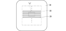
- FIG. 1 is a plan view schematically showing a top structure of an entire semiconductor device according to an embodiment
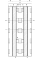
- FIG. 2 is an enlarged plan view of area "X" indicated in FIG. 1
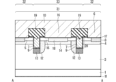
- FIG. 3 is a cross-sectional view taken along line AA of FIG. 2
- FIG. 3 is a cross-sectional view taken along line BB of FIG. 2
- FIG. 3 is a cross-sectional view taken along line CC of FIG. 2
- FIG. 4 is a schematic diagram for explaining the effect produced by the trench gate type MOSFET of the present embodiment
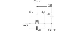
- 3 is an equivalent circuit diagram of a transistor region
- FIG. 3 is an equivalent circuit diagram including a transistor region and a dummy region
- FIG. FIG. 9 is an equivalent circuit diagram when switching the trench gate type MOSFET at low speed in FIG.
- FIG. 9 is an equivalent circuit diagram when switching the trench gate type MOSFET at high speed in FIG.
- FIG. 3 is a modified example of a cross-sectional view taken along line CC of FIG. 2
- FIG. 11 is a plan view showing a modification of the configuration of the characterizing portion of a trench gate type MOSFET formed on a silicon carbide semiconductor substrate
- 13 is a cross-sectional view taken along line AA of FIG. 12
- FIG. FIG. 13 is a cross-sectional view taken along line BB of FIG. 12
- FIG. 13 is a cross-sectional view along line CC of FIG. 12
- 1 is a plan view schematically showing the configuration of a trench gate type MOSFET of this embodiment
- FIG. 1 is a plan view schematically showing the configuration of a trench gate type MOSFET of this embodiment
- FIG. 1 is a plan view schematically showing the configuration of a trench gate type MOSFET of this embodiment
- FIG. 1 is a cross-sectional view schematically showing the configuration of a trench gate type MOSFET of this embodiment
- FIG. 10 is a cross-sectional view schematically showing a modification of the configuration of the trench gate type MOSFET of the present embodiment
- FIG. 10 is a cross-sectional view schematically showing a modification of the configuration of the trench gate type MOSFET of the present embodiment
- 1 is a plan view schematically showing the configuration of a trench gate type MOSFET of this embodiment
- FIG. 10 is a plan view showing a modification of the configuration of the characterizing portion of a trench gate type MOSFET formed on a silicon carbide semiconductor substrate (SiC substrate); BRIEF DESCRIPTION OF THE DRAWINGS It is a block diagram which shows the structure of the power conversion system to which the power converter regarding embodiment is applied.
- FIG. 10 is a plan view showing a modification of the configuration of the characterizing portion of a trench gate type MOSFET formed on a silicon carbide semiconductor substrate (SiC substrate);
- MOS Metal-Oxide-Semiconductor
- MOS transistor a field effect transistor having a MOS structure
- polycrystalline silicon has been adopted as the material of the gate electrode instead of metal, mainly from the viewpoint of forming the source-drain in a self-aligned manner.
- a material with a high dielectric constant is employed as the material of the gate insulating film, but the material is not necessarily limited to oxide.
- MOS is not necessarily limited only to the stacked structure of metal/oxide/semiconductor, and this specification does not presuppose such a limitation.
- MOS here is not only an abbreviation derived from its etymology, but also broadly includes the layered structure of conductor/insulator/semiconductor.
- n-type is generally defined as “first conductivity type” and p-type as “second conductivity type” with respect to the conductivity type of impurities, but the definition may be reversed.
- FIG. 1 is a plan view schematically showing the top structure of the entire semiconductor device according to the present embodiment.
- the semiconductor device according to the present embodiment has a rectangular outer shape, and at the center thereof is a minimum unit structure of a MOSFET (MOSFET cell) called a "unit cell”.
- MOSFET cell MOSFET cell
- a plurality of active regions 30 are provided, and the outer sides of the active regions 30 are surrounded by termination regions 34 .
- a plurality of gate trenches 20 are provided in parallel at intervals in the active region 30 .
- the plurality of gate trenches 20 are connected to gate wiring provided in the active region 30, and the gate wiring is connected to a gate pad, but illustration and description of these are omitted.
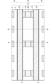
- FIG. 2 is an enlarged plan view of area "X" shown in FIG.
- the characteristic configuration shown in the region "X" will be described as this embodiment and its modification, and FIG. 1 is common to each embodiment and its modification.
- FIG. 2 is a plan view showing an example of the configuration of the characteristic portion of the semiconductor device of the present embodiment, more specifically, a trench gate type MOSFET formed on a silicon carbide semiconductor substrate (SiC substrate).
- the trench gate type MOSFET according to the present embodiment includes two adjacent gate trenches 20 and respective impurity regions (connection layer 12 and second well region) provided therebetween. including the region 14) constitute one unit cell 31.
- FIG. 1 is shown in FIG. 2, the trench gate type MOSFET according to the present embodiment includes two adjacent gate trenches 20 and respective impurity regions (connection layer 12 and second well region) provided therebetween. including the region 14) constitute one unit cell 31.
- FIG. 1 the trench gate type MOSFET according to the present embodiment includes two adjacent gate trenches 20 and respective impurity regions (connection layer 12 and second well region) provided therebetween. including the region 14) constitute one unit cell 31.
- the gate trenches 20 are provided in stripes so as to extend in a direction parallel to the off direction of the silicon carbide semiconductor substrate, and divide the active regions 30 into MOSFET cell units.
- the inner wall of gate trench 20 is covered with gate insulating film 7 , and gate electrode 9 is embedded in the region surrounded by gate insulating film 7 .
- the active region 30 between the gate trenches 20 is provided with a first contact 6 and a second contact 16 penetrating through an interlayer insulating film (here, not shown).
- One or more first well contact regions 8 are provided on the bottom surface of the first contact 6
- a second well contact region 18 is provided on the bottom surface of the second contact 16 .
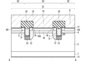
- FIG. 3 is a cross-sectional view along line AA in FIG.
- FIG. 4 is a cross-sectional view taken along line BB of FIG.
- FIG. 5 is a cross-sectional view taken along line CC of FIG. 3, 4 and 5 show the periodic structure of the unit cell 31 at a position including the gate trench 20 in cross section in the active region 30.
- FIG. 2 the configuration above the connection layer 12 in the drift layer 3 is omitted for the sake of convenience so that the arrangement of the connection layer 12 in the drift layer 3 can be understood.
- the trench gate MOSFET of the present embodiment includes n-type drift layer 3 provided on one main surface (first main surface) of silicon carbide semiconductor substrate 1 and , a gate trench 20 provided in the drift layer 3 extending in the first direction (the depth direction of the paper surface in FIG. 3), and a p-type trench 20 provided in the upper layer portion of the drift layer 3 and extending in the first direction.
- First contact 6 electrically connected to electrode 10 is separated by gate trench 20 in a second direction (a direction along the first main surface of silicon carbide semiconductor substrate 1) orthogonal to the first direction.
- a p-type second well region 14 extending in the first direction and having no n-type impurity region therein; , a p-type second well contact region 18, and a second contact electrically connected to the second well contact region 18 and electrically connected to the source electrode 10 provided above the drift layer 3.
- p-type electric field relaxation region 13 provided in contact with the bottom of gate trench 20, and a second direction (silicon carbide semiconductor provided in the drift layer 3 so as to be in contact with the sidewall of at least one of the gate trenches 20 in the direction along the first main surface of the substrate 1, and the electric field relaxation regions 13 and the second well regions 14 It has a p-type connection layer 12 for electrical connection and a drain electrode 11 provided below the drift layer 3 .
- a gate electrode 9 is provided via the film 7 .
- An interlayer insulating film 19 is provided so as to cover the gate trenches 20 and their surroundings. contacts 16 (contact openings) are respectively formed. The bottom surfaces of the first contact 6 and the second contact 16 are covered with a silicide film 17 , and the source electrode 10 is connected to the first contact 6 and the second contact 16 .
- silicon carbide semiconductor substrate 1 has a polytype of 4H, and the main surface of silicon carbide semiconductor substrate 1 and the main surface of drift layer 3 have an off angle ⁇ inclined in the [11-20] axial direction ( 0001) plane.
- the off angle ⁇ may be, for example, 10° or less.
- the first well region 4 in the upper layer portion of the drift layer 3 is provided in an active region 30 in which MOSFET cells are arranged, and selectively (partially) in the first well region 4, the first A source region 5 and a first well contact region 8 are provided.
- the first well contact region 8 is surrounded by the first source region 5 in plan view, as shown in FIG.
- the second well region 14 in the upper layer portion of the drift layer 3 is provided within the active region 30 in which the MOSFET cells are arranged.
- a well contact region 18 is provided.
- the second well contact region 18 is surrounded by the second well region 14 in plan view as shown in FIG.
- a gate electrode 9 is embedded in the gate trench 20 with the gate insulating film 7 interposed therebetween, and the top surface of the gate electrode 9 is located deeper than the outermost surface of the first source region 5 . That is, the upper surface of gate electrode 9 is located at a position recessed from the opening end of gate trench 20 . This is the same for the cross section taken along line BB, an example of which is shown in FIG.
- the electric field relaxation region 13 provided under the bottom surface of the gate trench 20 is provided for relaxing the electric field applied to the bottom surface and side surfaces of the gate trench 20 when the MOSFET is turned off, and is preferably in contact with the gate trench 20. .
- connection layer 12 provided so as to be in contact with the side surface of the electric field relaxation region 13 and part of the side wall of the gate trench 20 is also in contact with the second well region 14 so as to separate the electric field relaxation region 13 and the second well region 14 . It plays a role of electrically connecting with the well region 14 .
- a region including the second well region 14 is a dummy region 33 and a region other than the dummy region 33 that functions as a transistor is a transistor region 32 .
- connection layer 12 only contacts part of the sidewalls of the gate trenches 20, in FIG. It is provided continuously or discontinuously only on the side wall on the side in contact with 14 .
- An inversion channel is formed on the side wall of the gate trench 20 on the side contacting the first well region 4 under gate bias, and functions as a channel region of the MOSFET. At this time, the channel characteristics of each side wall of the gate trench 20 are substantially the same and are configured so as not to be non-uniform.
- the drift layer 3 has an off-angle in the ⁇ 11-20> direction, it is not affected by the anisotropy of the electrical characteristics caused by the difference in the crystal plane between the side walls of the gate trench 20. Identical and uniform channel characteristics can be achieved.
- the gate trench 20 penetrates the first source region 5 , the n-type first source region 5 is formed in the portion corresponding to the corner of the opening end of the gate trench 20 .
- the upper surface of the gate electrode 9 recedes from the opening end of the gate trench 20 at the corners of the opening end of the gate trench 20 , so that the first source region 5 and the gate electrode 9 do not face each other with the gate insulating film 7 interposed therebetween.
- the active region 30 as a whole does not have to have the planar configuration and cross-sectional configuration illustrated in FIGS. It may be Moreover, there is no limit to the ratio of the cross-sectional configurations shown in FIGS. 3 to 5, and configurations such as a configuration in which one side is large and the other side is small can be freely set.
- FIG. 23 is a modification of the cross-sectional view taken along line AA in FIG. As shown in FIG. 23, the first well contact region 8A and the second well contact region 18A are formed on the entire bottom surfaces of the first contact 6 and the second contact 16, respectively. I don't mind.
- FIG. 11 is a modified example of a cross-sectional view taken along line CC of FIG. As an example is shown in FIG. 11, a region in which the second contact 16 is not formed may be provided in the direction in which the gate trench 20 extends.
- the impurity concentration (cm ⁇ 3 ) indicates the peak value of the impurity concentration in the respective impurity layers and impurity regions.
- Nitrogen (N) or phosphorus (P) may be used as the n-type impurity, and aluminum (Al) or boron (B) may be used as the p-type impurity.
- n-type silicon carbide semiconductor substrate 1 in a wafer state having a polytype of 4H First, on one main surface of n-type silicon carbide semiconductor substrate 1 in a wafer state having a polytype of 4H, relatively high-resistance carbonization having a relatively low n-type impurity concentration (n ⁇ ) is formed.
- a drift layer 3 of silicon is formed by epitaxial growth. At this time, the drift layer 3 is formed so that the impurity concentration thereof is 1 ⁇ 10 14 cm ⁇ 3 or more and 1 ⁇ 10 17 cm ⁇ 3 or less.
- RIE reactive ion etching
- photolithography is performed with reference to the alignment marks formed on the dicing lines
- an ion implantation mask is formed on the drift layer 3, and the ion implantation is performed.
- Impurity ion implantation is performed through a mask.
- a p-type first well region 4 and a p-type second well region 14 are formed in the upper layer portion of the drift layer 3, and furthermore, the upper layer portion of the p-type first well region 4 is formed.
- a first source region 5 having a relatively low resistance and having a relatively high n-type impurity concentration (n + ) is formed in the region.
- the ion implantation mask for example, a resist mask or the like is used.
- first source region 5 has an impurity concentration of, for example, 5 ⁇ 10 18 cm ⁇ 3 or more and 5 ⁇ 10 20 cm ⁇ 3 or less
- first well region 4 and second well region 4 have an impurity concentration of 5 ⁇ 10 20 cm ⁇ 3 or less.
- Region 14 is formed to have an impurity concentration of, for example, 1 ⁇ 10 16 cm ⁇ 3 or more and 3 ⁇ 10 19 cm ⁇ 3 or less.
- the n-type impurity concentration of the first source region 5 is equal to that of the first well region 4 is set higher than the p-type impurity concentration of .
- the concentration in the first well region 4 and the second well region 14 may or may not be constant in the depth direction.
- the distribution may be such that the surface concentration is low, or the distribution may be such that it has a peak in the depth direction.
- a p-type first well contact region 8 is formed in the first source region 5, and a p-type second well contact region 18 is formed in the second well region 14 by ion implantation.
- the first well contact region 8 and the second well contact region 18 have a p-type impurity concentration of, for example, 1 ⁇ 10 19 cm ⁇ 3 or more and 1 ⁇ 10 22 cm ⁇ 3 or less. to form.
- the thickness of the first well contact region 8 is formed to be equal to or greater than the thickness of the first source region 5, so that the first well contact region 8 becomes the first well. Ensure contact with area 4.
- the formation order of impurity layers and impurity regions formed in drift layer 3 is not limited to the case described in the present embodiment.
- an etching mask having openings corresponding to the forming regions of the gate trenches 20 on the drift layer 3 is patterned.
- the alignment marks may be used as a reference.
- a gate trench 20 is formed through the first source region 5, the first well region 4 and the second well region 14 in the thickness direction and reaching the drift layer 3 by RIE using an etching mask. .
- electric field relaxation region 13 has an impurity concentration of, for example, 1 ⁇ 10 17 cm ⁇ 3 or more and 1 ⁇ 10 20 cm ⁇ 3 or less.
- the ion implantation mask is patterned using a resist material.
- the ion implantation mask has a pattern in which openings are provided only in portions of the gate trenches 20 that include the side walls where the connection layer 12 is provided, and openings are provided in portions including the side walls where the connection layer 12 is not provided. Not provided.
- connection layer 12 is performed by tilting silicon carbide semiconductor substrate 1 in the wafer state. and 60 degrees or less, the impurity concentration is, for example, 5 ⁇ 10 16 cm ⁇ 3 or more and 1 ⁇ 10 20 cm ⁇ 3 or less, and the depth from the surface is 0.3 ⁇ m or more. .
- connection layer 12 is formed after the electric field relaxation region 13 is formed.
- the gate trench 20 may be formed in accordance with the formation positions of the electric field relaxation region 13 and the connection layer 12 .
- the ion implantation mask used for the ion implantation of the electric field relaxation region 13 for the formation of the gate trench 20 .
- the ion implantation for forming the connection layer 12 may be performed perpendicularly to the wafer.
- annealing for activating the implanted ions is performed at a temperature range of 1500° C. or more and 2200° C. or less for a time of 0.5 minutes or more and 60 minutes or less.
- a field insulating film (not shown here) is formed.
- the gate insulating film 7 is formed to cover the inner wall surface of the gate trench 20 and the periphery of the gate trench 20 by thermal oxidation, CVD, or the like.
- a conductor layer such as polysilicon containing a relatively high concentration of impurities is formed by CVD or the like.
- the polysilicon not only grows vertically from the bottom surface of the gate trench 20 but also grows horizontally from the side surface of the gate trench 20 .
- Polysilicon is relatively easily buried inside.
- the polysilicon on the drift layer 3 is removed by etching.
- the polysilicon formed on the surface of the drift layer 3 is removed by etching, but the polysilicon buried inside the gate trench 20 remains because of its large film thickness, and constitutes the gate electrode 9 .
- the upper surface of gate electrode 9 inside trench 20 is formed at a position recessed from the open end of gate trench 20 .
- the interlayer insulating film 19 After forming the interlayer insulating film 19 so as to cover the termination region 34 (see FIG. 1) and the active region 30 , formation regions of the first contact 6 and the second contact 16 are formed on the interlayer insulating film 19 .
- a resist material is used to pattern an etching mask having openings in portions corresponding to . When forming this etching mask, the alignment marks may be used as a reference.
- the interlayer insulating film 19 is formed to cover the termination region 34 (see FIG. 1) and the active region 30, the entire surface of the active region 30 is dry-etched to form the first contact 6 and the second contact. Contacts 16 may be formed.
- the interlayer insulating film 19 formed on the surface of the drift layer 3 is removed by etching. , and maintains the function of electrically insulating the gate electrode 9 and the source electrode 10 .
- the etching mask may be provided with an opening for forming a gate contact (here, not shown) formed in the termination region 34 (see FIG. 1).
- a gate contact here, not shown
- the interlayer insulating film 19 may be removed and the gate contact may be formed at the same time.
- the first contact 6, the second contact 16 and the gate contact may be formed in separate steps.
- a metal film such as nickel is formed by a sputtering method or the like so as to cover the first contact 6, the second contact 16 and the interlayer insulating film 19.
- a metal film such as nickel is formed by a sputtering method or the like so as to cover the first contact 6, the second contact 16 and the interlayer insulating film 19.
- FIG. After that, for example, by performing annealing at 300° C. or more and 1200° C. or less, the first source region 5 and the first well contact exposed at the bottom surface of the first contact 6 and the bottom surface of the second contact 16 are exposed.
- a metal silicide film (here, NiSi 2 film) is formed over the region 8 and the second well contact region 18 to form a silicide film 17 to form an ohmic contact.
- the ohmic contact is not formed and the Schottky contact is formed.
- the source electrode 10 is formed by a sputtering method or the like so as to bury the first contact 6 and the second contact 16, and the source electrode 10 is formed in the first source region 5, the first well contact region 8 and the second well contact region 8. It is electrically connected to well contact region 18 .
- a cross-sectional configuration examples of which are shown in FIGS. 3 and 4, can be obtained.
- a gate pad or a wiring for connection to the gate pad is formed from the inside of the gate contact (not shown) to the upper portion.
- the drain electrode 11 is formed on the other main surface of the silicon carbide semiconductor substrate 1 by sputtering or the like, thereby obtaining the trench gate type MOSFET whose examples are shown in FIGS.
- connection layer 12 contacts one side surface of the electric field relaxation region 13 .
- Connection layer 12 also contacts second well region 14 . Therefore, electric field relaxation region 13 is electrically connected to second well region 14 .
- connection layer 12 secures a current path for a displacement current that flows as the depletion layer formed in the pn junction expands and contracts.
- the electric field relaxation region 13 When the connection layer 12 is not provided, the electric field relaxation region 13 has a floating potential, so that the potential follow-up of the electric field relaxation region 13 to the ON/OFF operation of the MOSFET becomes slow. As a result, the response speed of the depletion layer formed by the pn junction becomes slow, resulting in a structure that is difficult to turn off and turn on. As a result, switching loss increases.
- connection layer 12 By providing the connection layer 12, the response speed of the depletion layer formed by the pn junction can be increased, and switching loss can be reduced.
- connection layer 12 Since the connection layer 12 is formed only on the sidewall of the gate trench 20 on the side contacting the second well region 14, the channel density does not decrease, and the on-resistance increases due to the provision of the connection layer 12. can be suppressed. In addition, uniform channel characteristics can be realized by making the trench side wall where the connection layer 12 is not formed to be the trench side wall extending in the direction parallel to the off-direction. As a result, concentration of current on a specific channel surface is suppressed, and a MOSFET with high operational stability can be realized without instability of the threshold voltage.
- connection layer 12 is formed only on the sidewall of the gate trench 20 on the side contacting the second well region 14 , the first well region 4 and the electric field relaxation region 13 are electrically separated in the active region 30 . not properly connected. In other words, the first well region 4 and the second well region 14 are not electrically connected in the active region 30 . That is, current for charging/discharging the pn junction formed by electric field relaxation region 13 and drift layer 3 mainly flows through second well region 14 . Therefore, it is possible to suppress the potential fluctuation occurring in the first well region 4 during the switching operation, and it is possible to realize a MOSFET with high operational stability.
- the first well region 4 and the second well region 14 may be electrically connected in the termination region 34, and this does not limit the effect of realizing a MOSFET with high operational stability. .
- FIG. 6 is a schematic diagram for explaining the effect produced by the trench gate type MOSFET of this embodiment.
- FIG. 7 is an equivalent circuit diagram of the transistor region 32. As shown in FIG. In FIG. 7, illustration of the contact resistance ⁇ a is omitted for the sake of convenience.
- FIG. 8 is an equivalent circuit diagram combining the transistor region 32 and the dummy region 33. As shown in FIG. In FIG. 8, contact resistances ⁇ a and ⁇ b are omitted for convenience.
- Cgs is the capacitance between the gate electrode 9 and the source electrode 10 (hereinafter referred to as gate-source capacitance), and Cgd is the capacitance between the gate electrode 9 and the drain electrode 11 (hereinafter referred to as gate-drain capacitance).
- Cds is the capacitance between the drain electrode 11 and the source electrode 10 (hereinafter referred to as drain-source capacitance)
- Cgp is the capacitance between the gate electrode 9 and the second well region 14 (hereinafter referred to as , gate-well capacitance)
- Cdp is the capacitance between the drain electrode 11 and the second well region 14 (hereinafter referred to as drain-well capacitance).
- Rp is the resistance component of the connection layer 12, the electric field relaxation region 13 and the second well region 14; contact resistance.
- a region including the second well region 14 is a dummy region 33 and a region other than the dummy region 33 that functions as a transistor is a transistor region 32 .
- FIG. 9 is an equivalent circuit diagram when switching the trench gate type MOSFET at low speed in FIG. In FIG. 9, gate-well capacitance Cgp is removed from the circuit diagram shown in FIG.
- a displacement current is generated in the electric field relaxation region 13 and the second well region 14 due to charging and discharging of the drain-well capacitance Cdp. Since the impedance is sufficiently large, the displacement current mainly flows to the source electrode 10 via the resistance component Rp.
- FIG. 10 is an equivalent circuit diagram when switching the trench gate type MOSFET at high speed in FIG.
- resistance component Rp of electric field relaxation region 13 and second well region 14 is removed from the circuit diagram shown in FIG.
- a displacement current is generated in the electric field relaxation region 13 and the second well region 14 due to charging and discharging of the drain-well capacitance Cdp. Since the impedance is sufficiently smaller than Rp, the displacement current mainly flows to the gate electrode 9 via the gate-well capacitance Cgp.
- the effective capacitive coupling between the drain electrode 11 and the gate electrode 9 becomes larger than in the case of low-speed switching.
- connection layer 12 extends from the sidewall of the gate trench 20 in a direction (second direction, left-right direction in FIG. 3) perpendicular to the extending direction of the gate trench 20 (first direction, left-right direction in FIG. 2). provided to exist.
- Drift layer 3 between adjacent gate trenches 20 may be blocked by two opposing connection layers 12, but in order to increase the pn junction capacitance formed by connection layer 12 and drift layer 3, drift More preferably, layer 3 is not interrupted.
- connection layers 12 are provided separated from each other along the extending direction of the gate trenches 20 (the first direction, the horizontal direction in FIG. 2), and an example is shown in FIG. As shown, the connecting layer 12 may be provided continuously in the first direction.
- FIG. 24 is a plan view showing a modification of the configuration of the characterizing portion of a trench gate type MOSFET formed on a silicon carbide semiconductor substrate (SiC substrate).
- connection layer 12A is provided continuously along the direction in which the gate trench 20 extends.
- FIG. 26 is a plan view showing a modification of the configuration of the characterizing portion of a trench gate type MOSFET formed on a silicon carbide semiconductor substrate (SiC substrate). 26 are the same as those in FIGS. 3 and 4, respectively.
- the first well contact region 8 and the second well contact region 18 are discontinuously formed in the extending direction of the gate trench 20, but in FIG.
- Well contact region 8B and second well contact region 18B are formed continuously in the direction in which gate trench 20 extends. Even when such a configuration is adopted, it is possible to suppress an increase in switching loss and reduce electromagnetic noise.
- FIG. 12 is a plan view showing a modification of the configuration of the characterizing portion of a trench gate type MOSFET formed on a silicon carbide semiconductor substrate (SiC substrate).
- FIG. 13 is a cross-sectional view along line AA in FIG. 14 is a cross-sectional view taken along line BB of FIG. 12.
- FIG. 15 is a cross-sectional view taken along line CC of FIG. 12.
- FIG. 13, 14 and 15 show the periodic structure of the unit cell 31 at a position including the gate trench 20 in cross section in the active region 30.
- the second well region 14 was provided with the second well contact region 18, but in the configuration shown in FIG. 2 of the well contact region 18, an n-type second source region 15 having a smaller area than the first source region 5 in plan view is provided.
- a second source region 15 is provided in the upper layer portion of the second well region 14 and contacts the side surface of the second well contact region 18 .
- the n-type impurity concentration of the second source region 15 should be, for example, 5 ⁇ 10 18 cm ⁇ 3 or more and 5 ⁇ 10 20 cm ⁇ 3 or less, like the first source region 5. is preferred.
- FIG. 16 is a plan view schematically showing the configuration of the trench gate type MOSFET of this embodiment.
- the n-type second source region 15 extends in the extending direction of the gate trench 20 (first direction, right and left in FIG. 16). direction) (second direction, left-right direction in FIG. 3), the connection layer 12 or the second well contact region 18 are not flush with each other. That is, the second source region 15 is not located in the cross section taken along line AA in FIG. Similarly, the second source region 15 is not located in the cross section taken along line BB of FIG.
- FIG. 17 is a plan view schematically showing the configuration of the trench gate type MOSFET of this embodiment.
- the p-type second well contact region 18C has a larger area in plan view than the first well contact region 8. is small.
- ⁇ b can be increased, and effective capacitive coupling between the drain electrode 11 and the gate electrode 9 can be increased in the high frequency region. Therefore, the effect of reducing electromagnetic noise can be enhanced.
- FIG. 18 is a plan view schematically showing the configuration of the trench gate type MOSFET of this embodiment.
- a direction second , the left-right direction in FIG. 3
- the connection layer 12 and the second well contact region 18 are not located on the same plane.
- the connection layer 12 is located and the second well contact region 18 is not located.
- the second well contact region 18 is located and the connection layer 12 is not located in the cross section along line BB in FIG.
- the resistance component Rp can be increased, and the effective capacitive coupling between the drain electrode 11 and the gate electrode 9 can be increased in the high frequency region. Therefore, the effect of reducing electromagnetic noise can be enhanced.
- the impurity concentration of the second well region 14 forming the dummy region 33 in FIG. 3 is equal to the impurity concentration of the first well region 4 forming the transistor region 32 in FIG. lower than
- the resistance component Rp of the second well region 14 can be increased, and the effective capacitive coupling between the drain electrode 11 and the gate electrode 9 can be increased in the high frequency region. Therefore, the effect of reducing electromagnetic noise can be enhanced.
- the impurity concentration of the second well region 14 may be even slightly lower than the impurity concentration of the first well region 4.
- the effect can be obtained by reducing the impurity concentration by several percent to several tens of percent.
- the length of the two well regions 14 is formed smaller than the width of the first well region 4 (in that direction) that constitutes the transistor region 32 in FIG.
- the resistance component Rp of the second well region 14 can be increased, and the effective capacitive coupling between the drain electrode 11 and the gate electrode 9 can be increased in the high frequency region. Therefore, the effect of reducing electromagnetic noise can be enhanced.
- the width of the second well region 14 may be made even slightly smaller than the width of the first well region 4. For example, the effect can be obtained by reducing the width by several percent to several tens of percent.
- FIG. 19 is a cross-sectional view schematically showing the structure of the trench gate type MOSFET of this embodiment. The corresponding plan view is similar to FIG.
- the impurity concentration of the high-concentration region 21 is preferably lower than the p-type impurity concentration of the connection layer 12 , the electric field relaxation region 13 and the second well region 14 .
- the impurity concentration of the high-concentration region 21 is set higher than that of the drift layer 3 .
- the drain-well capacitance Cdp can be increased, and the effective capacitive coupling between the drain electrode 11 and the gate electrode 9 can be increased in the high frequency region. Therefore, the effect of reducing electromagnetic noise can be enhanced.
- FIG. 20 is a cross-sectional view schematically showing a modification of the configuration of the trench gate type MOSFET of this embodiment. The corresponding plan view is similar to FIG.
- the high concentration region 21A is provided not only directly below the second well region 14 but also directly below the first well region 4. As shown in FIG. 20, in the trench gate type MOSFET, the high concentration region 21A is provided not only directly below the second well region 14 but also directly below the first well region 4. As shown in FIG. 20, in the trench gate type MOSFET, the high concentration region 21A is provided not only directly below the second well region 14 but also directly below the first well region 4. As shown in FIG. 20, in the trench gate type MOSFET, the high concentration region 21A is provided not only directly below the second well region 14 but also directly below the first well region 4. As shown in FIG.
- the impurity concentration of the high-concentration region 21A is preferably lower than that of the first well region 4. This is because the depletion layers formed by the pn junctions formed between the high-concentration region 21A and the first well region 4 and between the high-concentration region 21A and the electric field relaxation region 13 are shifted toward the high-concentration region 21A side. This is for stretching.
- the impurity concentration of the high-concentration region 21A is made higher than that of the drift layer 3.
- FIG. 21 is a cross-sectional view schematically showing a modification of the configuration of the trench gate type MOSFET of this embodiment. The corresponding plan view is similar to FIG.
- the high-concentration region 21 as shown in FIG. 21 is formed by forming the gate trench 20, removing the etching mask, and implanting n-type impurity ions from an oblique direction to form the side wall of the gate trench 20 and the electric field. It is formed in contact with the relaxation region 13 .
- the high concentration region 21 is formed directly under the second well region 14 or directly under the first well region 4 and directly under the second well region 14 . The effects produced by this configuration are similar to those produced by the configurations shown in FIGS.
- FIG. 22 is a plan view schematically showing the configuration of the trench gate type MOSFET of this embodiment.
- the first source regions 5 are discontinuously formed in the extending direction of the first well region 4 .
- the impurity concentrations of the p-type impurities in the first well contact region 8 and the second well contact region 18 are the same.
- the contact resistivity ( ⁇ cm 2 ) is also the same, for example, the opening area of the second contact 16 above the second well contact region 18 is the same as that of the first well contact region 8 of the first contact 6 .
- the contact resistance ⁇ a to the second well contact region 18 can be made larger than the contact resistance ⁇ b to the first well contact region 8 .
- the contact resistance .rho it can be made larger than the contact resistance ⁇ b for the contact region 8 .
- the contact resistance ⁇ b (see FIG. 6) with respect to the second well contact region 18 can be increased, and the effective capacitive coupling between the drain electrode 11 and the gate electrode 9 can be increased in the high frequency region. can be done. Therefore, the effect of reducing electromagnetic noise can be enhanced.
- the first well contact region 8 and the second well contact region 18 have the same p-type impurity concentration, and the contact resistivity ( ⁇ cm 2 ) is , the contact resistivity for the second well contact region 18 can also be formed to be greater than the contact resistivity for the first well contact region 8 .
- the above can be realized by setting the impurity concentration of the p-type impurities on the outermost surface of the second well contact region 18 to be lower than the impurity concentration of the p-type impurities on the outermost surface of the first well contact region 8. be.
- the contact resistance ⁇ b (FIG. 6) with respect to the second well contact region 18 can be increased, and the effective capacitive coupling between the drain electrode 11 and the gate electrode 9 can be increased in the high frequency region. . Therefore, the effect of reducing electromagnetic noise can be enhanced.
- the semiconductor devices according to the first to eighth embodiments are applied to a power converter.
- the present embodiment is not limited to application to a specific power converter, a case where the semiconductor device described above is applied to a three-phase inverter will be described below as a ninth embodiment.
- FIG. 25 is a block diagram showing the configuration of a power conversion system to which the power conversion device according to this embodiment is applied.
- the power conversion system shown in FIG. 25 includes a power supply 500, a power conversion device 600, and a load 700.
- the power supply 500 is a DC power supply and supplies DC power to the power conversion device 600 .
- the power supply 500 can be configured with various devices, for example, it can be configured with a DC system, a solar battery, or a storage battery, or it can be configured with a rectifier circuit or an AC/DC converter connected to an AC system. may Also, power supply 500 may be configured by a DC/DC converter that converts DC power output from a DC system into predetermined power.
- the power conversion device 600 is a three-phase inverter connected between the power supply 500 and the load 700 , converts the DC power supplied from the power supply 500 into AC power, and supplies the AC power to the load 700 . As shown in FIG. 25, the power conversion device 600 outputs a main conversion circuit 601 that converts DC power into AC power and outputs a drive signal that drives the switching elements of the main conversion circuit 601. A drive circuit 602 and a control circuit 603 that outputs a control signal for controlling the drive circuit 602 to the drive circuit 602 are provided.
- a load 700 is a three-phase electric motor driven by AC power supplied from the power converter 600 .
- the load 700 is not limited to a specific application, and is an electric motor mounted on various electrical equipment, such as a hybrid vehicle, an electric vehicle, a railroad vehicle, an elevator, or an electric motor for air conditioning equipment.
- the main conversion circuit 601 includes a switching element and a freewheeling diode (here, not shown). By switching the switching element, the DC power supplied from the power supply 500 is converted into AC power and supplied to the load 700. do.
- the main conversion circuit 601 has various specific circuit configurations, the main conversion circuit 601 according to the present embodiment is a two-level three-phase full bridge circuit, and has six switching elements and an inverse switching element for each switching element. It can consist of six freewheeling diodes in parallel.
- the semiconductor device according to any one of the first to eighth embodiments is applied to each switching element of the main conversion circuit 601 .
- the six switching elements are connected in series every two switching elements to form upper and lower arms, and the respective upper and lower arms form respective phases (U phase, V phase, W phase) of the full bridge circuit.
- Output terminals of the respective upper and lower arms, that is, three output terminals of the main conversion circuit 601 are connected to the load 700 .
- the drive circuit 602 generates a drive signal for driving the switching element of the main conversion circuit 601 and supplies it to the control electrode of the switching element of the main conversion circuit 601 .
- a drive signal for turning on a switching element and a drive signal for turning off a switching element are output to control electrodes of the respective switching elements.
- the driving signal When maintaining the switching element in the ON state, the driving signal is a voltage signal (ON signal) equal to or higher than the threshold voltage of the switching element, and when maintaining the switching element in the OFF state, the driving signal is equal to the threshold voltage of the switching element. It becomes a voltage signal (OFF signal) below the voltage.
- the control circuit 603 controls the switching elements of the main conversion circuit 601 so that the desired power is supplied to the load 700 . Specifically, based on the power to be supplied to the load 700, the time (on time) during which each switching element of the main conversion circuit 601 should be in the ON state is calculated. For example, the main conversion circuit 601 can be controlled by PWM control that modulates the ON time of the switching element according to the voltage to be output. Then, a control command (control signal) is output to the drive circuit 602 so that an ON signal is output to the switching element that should be in the ON state at each time point, and an OFF signal is output to the switching element that should be in the OFF state. The drive circuit 602 outputs an ON signal or an OFF signal as a drive signal to the control electrode of each switching element according to this control signal.
- the semiconductor device according to any one of the first to eighth embodiments is applied as the switching element of the main conversion circuit 601
- An electric field applied to the bottom surface of the gate trench can be relaxed.
- the electric field relaxation region 13 at the bottom of the trench and the first well region 4 are electrically connected by the connection layer 12, the pn junction formed by the electric field relaxation region 13 at the bottom of the trench and the drift layer 3 is filled. A current path for discharging is secured, and switching loss can be reduced.
- the application is not limited to this, and can be applied to various power converters.
- a two-level power converter is used, but a three-level or multi-level power converter may be used.
- when power is supplied to a single-phase load it may be applied to a single-phase inverter.
- when power is supplied to a DC load or the like it can be applied to a DC/DC converter or an AC/DC converter.
- the power conversion device to which the above semiconductor device is applied is not limited to the case where the above load is an electric motor. It can also be used as a power supply device for a solar power generation system or a power storage system.
- the replacement may be made across multiple embodiments. In other words, it may be the case that the respective configurations whose examples are shown in the different embodiments are combined to produce the same effect.
- the semiconductor device includes a first semiconductor layer of a first conductivity type, a gate trench 20 and a first well region 4 of a second conductivity type (p-type). , a first impurity region of the first conductivity type, and at least one first well contact region 8 of the second conductivity type (p-type) (or the first well contact region 8A, the first well contact region 8A). contact region 8B), at least one first contact 6, a second well region 14 of the second conductivity type (p-type), and at least one second well region 14 of the second conductivity type (p-type).
- Well contact region 18 (or second well contact region 18A, second well contact region 18B, second well contact region 18C), at least one second contact 16, and a second conductivity type (p type) electric field relaxation region 13, a plurality of connection layers 12 (or connection layers 12A) of the second conductivity type (p-type), and a second main electrode.
- the first conductivity type first semiconductor layer corresponds to, for example, the n-type drift layer 3 or the like.
- the first impurity region of the first conductivity type corresponds to, for example, the n-type first source region 5 or the like.
- the second main electrode corresponds to, for example, the drain electrode 11 and the like.
- Gate trench 20 is provided on the upper surface of drift layer 3 to extend in a first direction along the upper surface of drift layer 3 (that is, the depth direction in FIG. 3).
- the first well region 4 is provided in the upper layer portion of the drift layer 3 and extends in the first direction.
- a first source region 5 is provided in an upper layer portion of the first well region 4 .
- a first well contact region 8 is provided in the upper layer of the first well region 4 and contacts the first source region 5 on the side surface.
- a first contact 6 is electrically connected to the first source region 5 and the at least one first well contact region 8 and electrically to a first main electrode provided above the drift layer 3 .
- the first main electrode corresponds to, for example, the source electrode 10 or the like.
- the second well regions 14 are separated by the gate trenches 20 in a second direction (that is, the horizontal direction in FIG. 3) along the upper surface of the drift layer 3 and perpendicular to the first direction, and , extending in the first direction and having no impurity region of the first conductivity type therein.
- a second well contact region 18 is provided in an upper layer portion of the second well region 14 .
- the second contact 16 is electrically connected to the second well contact region 18 and electrically connected to the source electrode 10 provided above the drift layer 3 .
- Electric field relaxation region 13 is provided in contact with the bottom of gate trench 20 .
- connection layer 12 is provided in contact with mutually opposing sidewalls (sidewalls in contact with the second well region 14 ) of the adjacent gate trenches 20 , and separates the electric field relaxation region 13 and the second well region 14 . Connect electrically. Drain electrode 11 is provided below drift layer 3 . Inside the gate trench 20, a gate insulating film is formed on the side surface of the first source region 5, the side surface of the first well region 4, the side surface of the second well region 14, the electric field relaxation region 13, and the connection layer 12. A gate electrode 9 is provided via 7 .
- the semiconductor device includes the drift layer 3, the gate trench 20, the first well region 4, the first source region 5, and the first well contact region. 8, a first contact 6, a second well region 14, a second well contact region 18, at least one second impurity region of the first conductivity type (n-type), and a second A contact 16 , an electric field relaxation region 13 , a connection layer 12 and a drain electrode 11 are provided.
- the second impurity region corresponds to, for example, the n-type second source region 15 or the like.
- the second well region 14 is provided separated by the gate trench 20 in a second direction along the upper surface of the drift layer 3, which is a direction orthogonal to the first direction, and extends in the first direction. .
- the second source region 15 is provided in the upper layer portion of the second well region 14, is in contact with the side surface of at least one second well contact region 18, and has an area of the first source region in plan view. less than 5. Also, the connection layer 12 is not provided on the side wall that contacts the first well region 4 . Inside the gate trench 20, a gate insulating film is formed on the side surface of the first source region 5, the side surface of the first well region 4, the side surface of the second well region 14, the electric field relaxation region 13, and the connection layer 12. A gate electrode 9 is provided via 7 .
- the effect of reducing the on-resistance can be obtained. Further, by providing the n-type second source region 15, even if the MOSFET is partially formed in the second well region 14, the region where the MOSFET exists in the first well region 4 and the second If there is a gate-well capacitance Cgp in the portion where the n-type region is not formed in the second well region 14 with respect to the sum of the region where the MOSFET is partially formed in the well region 14 of the second well region 14, The effect of reducing electromagnetic noise can be obtained in the same manner as the configuration in which the n-type region is not formed in the second well region 14 .
- the second source region 15 is not formed coplanar with the connection layer 12 or the second well contact region 18 in the second direction. According to such a configuration, it is possible to effectively reduce the on-resistance of the trench gate type MOSFET.
- the second well contact region 18C has a smaller area than the first well contact region 8 in plan view.
- the second well contact region 18 and the connection layer 12 are not formed on the same plane in the second direction.
- the resistance component Rp can be increased, and the effective capacitive coupling between the drain electrode 11 and the gate electrode 9 can be increased in the high frequency region. Therefore, the effect of reducing electromagnetic noise can be enhanced.
- the second well region 14 has a lower impurity concentration than the first well region 4 .
- the resistance component Rp of the second well region 14 can be increased, and the effective capacitive coupling between the drain electrode 11 and the gate electrode 9 can be increased in the high frequency region. . Therefore, the effect of reducing electromagnetic noise can be enhanced.
- the length of the second well region 14 in the second direction is shorter than the length of the first well region 4 in the second direction.
- the resistance component Rp of the second well region 14 can be increased, and the effective capacitive coupling between the drain electrode 11 and the gate electrode 9 can be increased in the high frequency region. . Therefore, the effect of reducing electromagnetic noise can be enhanced.
- the semiconductor device is provided below the second well region 14 and has a first conductivity type high concentration region having a higher impurity concentration than the drift layer 3 . 21 (or high concentration region 21A).
- the drain-well capacitance Cdp can be increased, and effective capacitive coupling between the drain electrode 11 and the gate electrode 9 can be increased in a high frequency region. Therefore, the effect of reducing electromagnetic noise can be enhanced.
- the high-concentration region 21A is also provided below the first well region 4 .
- the effect of reducing the on-resistance can be obtained.
- the first source regions 5 are formed discontinuously in the first direction. According to such a configuration, it is possible to arbitrarily set the trade-off relationship between the on-characteristics of the MOSFET and the withstand voltage. That is, by providing the portion where the first source region 5 is not formed, the voltage resistance can be improved, and by providing the portion where the first source region 5 is formed, the on-characteristics of the MOSFET can be improved. . Therefore, by adjusting the ratio of the portion where the first source region 5 is not formed and the portion where the first source region 5 is formed, it is possible to arbitrarily set the trade-off relationship between the on-characteristics of the MOSFET and the withstand voltage. can be done.
- the contact resistance of the at least one second contact 16 to the at least one second well contact region 18 is less than that of the at least one first contact 6 . greater than the contact resistance to the first well contact region 8.
- the contact resistance ⁇ b (FIG. 6) with respect to the second well contact region 18 can be increased, and the effective capacitive coupling between the drain electrode 11 and the gate electrode 9 can be improved in the high frequency region. can be increased. Therefore, the effect of reducing electromagnetic noise can be enhanced.
- the impurity concentration of at least one second well contact region 18 is lower than the impurity concentration of at least one first well contact region 8 .
- the contact resistance ⁇ b (FIG. 6) with respect to the second well contact region 18 can be increased, and the effective capacitive coupling between the drain electrode 11 and the gate electrode 9 can be improved in the high frequency region. can be increased. Therefore, the effect of reducing electromagnetic noise can be enhanced.
- the opening area of the at least one second contact 16 above the at least one second well contact region 18 is at least 100% of the at least one first contact 6 . smaller than the opening area on one first well contact region 8 .
- the material when a material name is described without being specified, unless there is a contradiction, the material contains other additives, such as an alloy. shall be included.
- each component in the embodiments described above is a conceptual unit, and within the scope of the technology disclosed in this specification, when one component is composed of a plurality of structures , the case where one component corresponds to a part of a structure, and further the case where a plurality of components are provided in one structure.
- each component in the embodiments described above includes structures having other structures or shapes as long as they exhibit the same function.
- first well region 6 first contact, 7 gate insulating film, 8 first well contact region, 8A first well contact region, 8B first well contact region, 9 gate electrode, 12 connection layer, 12A connection layer, 13 electric field relaxation region, 14 second well region, 16 second contact, 18 second well contact region, 18A second well contact region, 18B second well contact region, 18C second well contact region Well contact region, 20 gate trench, 21 high concentration region, 21A high concentration region, 600 power conversion device, 601 main conversion circuit, 602 drive circuit, 603 control circuit.
Landscapes
- Electrodes Of Semiconductors (AREA)
Priority Applications (2)
| Application Number | Priority Date | Filing Date | Title |
|---|---|---|---|
| JP2022561541A JP7337469B1 (ja) | 2022-03-03 | 2022-03-03 | 半導体装置および電力変換装置 |
| PCT/JP2022/009114 WO2023166657A1 (ja) | 2022-03-03 | 2022-03-03 | 半導体装置および電力変換装置 |
Applications Claiming Priority (1)
| Application Number | Priority Date | Filing Date | Title |
|---|---|---|---|
| PCT/JP2022/009114 WO2023166657A1 (ja) | 2022-03-03 | 2022-03-03 | 半導体装置および電力変換装置 |
Publications (1)
| Publication Number | Publication Date |
|---|---|
| WO2023166657A1 true WO2023166657A1 (ja) | 2023-09-07 |
Family
ID=87882047
Family Applications (1)
| Application Number | Title | Priority Date | Filing Date |
|---|---|---|---|
| PCT/JP2022/009114 Ceased WO2023166657A1 (ja) | 2022-03-03 | 2022-03-03 | 半導体装置および電力変換装置 |
Country Status (2)
| Country | Link |
|---|---|
| JP (1) | JP7337469B1 (https=) |
| WO (1) | WO2023166657A1 (https=) |
Cited By (1)
| Publication number | Priority date | Publication date | Assignee | Title |
|---|---|---|---|---|
| JP2023136822A (ja) * | 2022-03-17 | 2023-09-29 | 株式会社東芝 | 半導体装置、インバータ回路、駆動装置、車両、及び、昇降機 |
Families Citing this family (1)
| Publication number | Priority date | Publication date | Assignee | Title |
|---|---|---|---|---|
| US20250241040A1 (en) * | 2024-01-19 | 2025-07-24 | Wolfspeed, Inc. | Gate trench power semiconductor devices having deep trench shield connection patterns |
Citations (4)
| Publication number | Priority date | Publication date | Assignee | Title |
|---|---|---|---|---|
| JP2007134625A (ja) * | 2005-11-14 | 2007-05-31 | Mitsubishi Electric Corp | 半導体装置およびその製造方法 |
| JP2018082055A (ja) * | 2016-11-16 | 2018-05-24 | 富士電機株式会社 | 半導体装置および半導体装置の製造方法 |
| JP2018186270A (ja) * | 2017-04-24 | 2018-11-22 | インフィネオン テクノロジーズ アーゲーInfineon Technologies Ag | トレンチ下部にオフセットを有するSiC半導体デバイス |
| JP6753951B2 (ja) * | 2017-06-06 | 2020-09-09 | 三菱電機株式会社 | 半導体装置および電力変換装置 |
Family Cites Families (7)
| Publication number | Priority date | Publication date | Assignee | Title |
|---|---|---|---|---|
| JP4738562B2 (ja) * | 2000-03-15 | 2011-08-03 | 三菱電機株式会社 | 半導体装置の製造方法 |
| JP2014003191A (ja) * | 2012-06-20 | 2014-01-09 | Hitachi Ltd | 半導体装置 |
| JP6715567B2 (ja) * | 2014-12-16 | 2020-07-01 | 富士電機株式会社 | 半導体装置 |
| DE102014119465B3 (de) * | 2014-12-22 | 2016-05-25 | Infineon Technologies Ag | Halbleitervorrichtung mit streifenförmigen trenchgatestrukturen, transistormesas und diodenmesas |
| JP6253854B1 (ja) * | 2016-03-30 | 2017-12-27 | 三菱電機株式会社 | 半導体装置およびその製造方法、電力変換装置 |
| JP7029364B2 (ja) * | 2018-08-20 | 2022-03-03 | 株式会社東芝 | 半導体装置 |
| DE112019006587T5 (de) * | 2019-01-08 | 2021-12-23 | Mitsubishi Electric Corporation | Halbleitereinheit und leistungswandlereinheit |
-
2022
- 2022-03-03 JP JP2022561541A patent/JP7337469B1/ja active Active
- 2022-03-03 WO PCT/JP2022/009114 patent/WO2023166657A1/ja not_active Ceased
Patent Citations (4)
| Publication number | Priority date | Publication date | Assignee | Title |
|---|---|---|---|---|
| JP2007134625A (ja) * | 2005-11-14 | 2007-05-31 | Mitsubishi Electric Corp | 半導体装置およびその製造方法 |
| JP2018082055A (ja) * | 2016-11-16 | 2018-05-24 | 富士電機株式会社 | 半導体装置および半導体装置の製造方法 |
| JP2018186270A (ja) * | 2017-04-24 | 2018-11-22 | インフィネオン テクノロジーズ アーゲーInfineon Technologies Ag | トレンチ下部にオフセットを有するSiC半導体デバイス |
| JP6753951B2 (ja) * | 2017-06-06 | 2020-09-09 | 三菱電機株式会社 | 半導体装置および電力変換装置 |
Cited By (2)
| Publication number | Priority date | Publication date | Assignee | Title |
|---|---|---|---|---|
| JP2023136822A (ja) * | 2022-03-17 | 2023-09-29 | 株式会社東芝 | 半導体装置、インバータ回路、駆動装置、車両、及び、昇降機 |
| JP7783598B2 (ja) | 2022-03-17 | 2025-12-10 | 株式会社東芝 | 半導体装置、インバータ回路、駆動装置、車両、及び、昇降機 |
Also Published As
| Publication number | Publication date |
|---|---|
| JP7337469B1 (ja) | 2023-09-04 |
| JPWO2023166657A1 (https=) | 2023-09-07 |
Similar Documents
| Publication | Publication Date | Title |
|---|---|---|
| JP7134315B2 (ja) | 半導体装置および電力変換装置 | |
| US12295156B2 (en) | Semiconductor device including trench gate structure and buried shielding region and method of manufacturing | |
| CN111466032B (zh) | 碳化硅半导体装置以及电力变换装置 | |
| WO2017187670A1 (ja) | 半導体装置および電力変換装置 | |
| JP7778041B2 (ja) | 半導体装置および電力変換装置 | |
| JP6991370B2 (ja) | 半導体装置及び電力変換装置 | |
| JP6981585B1 (ja) | 半導体装置、電力変換装置、および半導体装置の製造方法 | |
| WO2020188686A1 (ja) | 炭化珪素半導体装置および電力変換装置 | |
| JP7337469B1 (ja) | 半導体装置および電力変換装置 | |
| JP7330396B2 (ja) | 半導体装置及び電力変換装置 | |
| WO2021044624A1 (ja) | 炭化珪素半導体装置および電力変換装置 | |
| US20250089308A1 (en) | Power semiconductor device and power converter including the same | |
| US20250120133A1 (en) | Gate trench power semiconductor devices having deep support shields and methods of fabricating such device | |
| CN119092548A (zh) | 功率器件、功率模块、功率转换电路和车辆 | |
| JP7841095B2 (ja) | 半導体装置、電力変換装置および半導体装置の製造方法 | |
| WO2020100960A1 (ja) | 半導体装置、電力変換装置、半導体装置の製造方法、および、電力変換装置の製造方法 | |
| JP7074267B1 (ja) | 半導体装置、電力変換装置及び半導体装置の製造方法 | |
| US20250203961A1 (en) | Power semiconductor device and power converter including the same | |
| CN110176487A (zh) | 半导体装置及其制造方法、电力变换装置 |
Legal Events
| Date | Code | Title | Description |
|---|---|---|---|
| WWE | Wipo information: entry into national phase |
Ref document number: 2022561541 Country of ref document: JP |
|
| 121 | Ep: the epo has been informed by wipo that ep was designated in this application |
Ref document number: 22929802 Country of ref document: EP Kind code of ref document: A1 |
|
| NENP | Non-entry into the national phase |
Ref country code: DE |
|
| 122 | Ep: pct application non-entry in european phase |
Ref document number: 22929802 Country of ref document: EP Kind code of ref document: A1 |