WO2023166657A1 - Semiconductor device and power conversion device - Google Patents
Semiconductor device and power conversion device Download PDFInfo
- Publication number
- WO2023166657A1 WO2023166657A1 PCT/JP2022/009114 JP2022009114W WO2023166657A1 WO 2023166657 A1 WO2023166657 A1 WO 2023166657A1 JP 2022009114 W JP2022009114 W JP 2022009114W WO 2023166657 A1 WO2023166657 A1 WO 2023166657A1
- Authority
- WO
- WIPO (PCT)
- Prior art keywords
- region
- well
- contact
- semiconductor device
- gate
- Prior art date
Links
- 239000004065 semiconductor Substances 0.000 title claims abstract description 94
- 238000006243 chemical reaction Methods 0.000 title claims description 29
- 239000012535 impurity Substances 0.000 claims abstract description 82
- 230000005684 electric field Effects 0.000 claims abstract description 65
- 239000004020 conductor Substances 0.000 claims description 3
- 230000000116 mitigating effect Effects 0.000 abstract 2
- 239000010410 layer Substances 0.000 description 136
- 230000000694 effects Effects 0.000 description 32
- HBMJWWWQQXIZIP-UHFFFAOYSA-N silicon carbide Chemical compound [Si+]#[C-] HBMJWWWQQXIZIP-UHFFFAOYSA-N 0.000 description 26
- 229910010271 silicon carbide Inorganic materials 0.000 description 26
- 239000000758 substrate Substances 0.000 description 23
- 230000004048 modification Effects 0.000 description 18
- 238000012986 modification Methods 0.000 description 18
- 230000008878 coupling Effects 0.000 description 17
- 238000010168 coupling process Methods 0.000 description 17
- 238000005859 coupling reaction Methods 0.000 description 17
- 238000010586 diagram Methods 0.000 description 14
- 238000005530 etching Methods 0.000 description 13
- 238000005468 ion implantation Methods 0.000 description 13
- 239000000463 material Substances 0.000 description 12
- 238000005516 engineering process Methods 0.000 description 11
- 238000006073 displacement reaction Methods 0.000 description 10
- 239000011229 interlayer Substances 0.000 description 10
- 229910021420 polycrystalline silicon Inorganic materials 0.000 description 9
- 229920005591 polysilicon Polymers 0.000 description 8
- 238000005229 chemical vapour deposition Methods 0.000 description 5
- 238000007599 discharging Methods 0.000 description 5
- 229910052751 metal Inorganic materials 0.000 description 5
- 239000002184 metal Substances 0.000 description 5
- 230000015572 biosynthetic process Effects 0.000 description 4
- 150000002500 ions Chemical class 0.000 description 4
- 238000000034 method Methods 0.000 description 4
- 230000010355 oscillation Effects 0.000 description 4
- 238000001020 plasma etching Methods 0.000 description 4
- 238000001312 dry etching Methods 0.000 description 3
- 238000004519 manufacturing process Methods 0.000 description 3
- 229910021332 silicide Inorganic materials 0.000 description 3
- FVBUAEGBCNSCDD-UHFFFAOYSA-N silicide(4-) Chemical compound [Si-4] FVBUAEGBCNSCDD-UHFFFAOYSA-N 0.000 description 3
- 238000004544 sputter deposition Methods 0.000 description 3
- IJGRMHOSHXDMSA-UHFFFAOYSA-N Atomic nitrogen Chemical compound N#N IJGRMHOSHXDMSA-UHFFFAOYSA-N 0.000 description 2
- PXHVJJICTQNCMI-UHFFFAOYSA-N Nickel Chemical compound [Ni] PXHVJJICTQNCMI-UHFFFAOYSA-N 0.000 description 2
- XUIMIQQOPSSXEZ-UHFFFAOYSA-N Silicon Chemical compound [Si] XUIMIQQOPSSXEZ-UHFFFAOYSA-N 0.000 description 2
- 238000000137 annealing Methods 0.000 description 2
- 238000009826 distribution Methods 0.000 description 2
- 230000005669 field effect Effects 0.000 description 2
- 230000003647 oxidation Effects 0.000 description 2
- 238000007254 oxidation reaction Methods 0.000 description 2
- 230000003071 parasitic effect Effects 0.000 description 2
- 230000000737 periodic effect Effects 0.000 description 2
- 230000004044 response Effects 0.000 description 2
- 229910052710 silicon Inorganic materials 0.000 description 2
- 239000010703 silicon Substances 0.000 description 2
- 238000003860 storage Methods 0.000 description 2
- ZOXJGFHDIHLPTG-UHFFFAOYSA-N Boron Chemical compound [B] ZOXJGFHDIHLPTG-UHFFFAOYSA-N 0.000 description 1
- 229910005881 NiSi 2 Inorganic materials 0.000 description 1
- OAICVXFJPJFONN-UHFFFAOYSA-N Phosphorus Chemical compound [P] OAICVXFJPJFONN-UHFFFAOYSA-N 0.000 description 1
- 230000003213 activating effect Effects 0.000 description 1
- 239000000654 additive Substances 0.000 description 1
- 238000004378 air conditioning Methods 0.000 description 1
- 229910045601 alloy Inorganic materials 0.000 description 1
- 239000000956 alloy Substances 0.000 description 1
- 229910052782 aluminium Inorganic materials 0.000 description 1
- XAGFODPZIPBFFR-UHFFFAOYSA-N aluminium Chemical compound [Al] XAGFODPZIPBFFR-UHFFFAOYSA-N 0.000 description 1
- 229910052796 boron Inorganic materials 0.000 description 1
- 238000003763 carbonization Methods 0.000 description 1
- 239000013078 crystal Substances 0.000 description 1
- 238000007667 floating Methods 0.000 description 1
- 238000002513 implantation Methods 0.000 description 1
- 238000009413 insulation Methods 0.000 description 1
- 239000012212 insulator Substances 0.000 description 1
- 230000010354 integration Effects 0.000 description 1
- 230000007257 malfunction Effects 0.000 description 1
- 229910044991 metal oxide Inorganic materials 0.000 description 1
- 150000004706 metal oxides Chemical class 0.000 description 1
- 229910052759 nickel Inorganic materials 0.000 description 1
- 229910052757 nitrogen Inorganic materials 0.000 description 1
- 230000000149 penetrating effect Effects 0.000 description 1
- 229910052698 phosphorus Inorganic materials 0.000 description 1
- 239000011574 phosphorus Substances 0.000 description 1
- 238000000206 photolithography Methods 0.000 description 1
- 238000010248 power generation Methods 0.000 description 1
- 230000002040 relaxant effect Effects 0.000 description 1
- 238000001039 wet etching Methods 0.000 description 1
Images


Classifications
-
- H—ELECTRICITY
- H01—ELECTRIC ELEMENTS
- H01L—SEMICONDUCTOR DEVICES NOT COVERED BY CLASS H10
- H01L29/00—Semiconductor devices adapted for rectifying, amplifying, oscillating or switching, or capacitors or resistors with at least one potential-jump barrier or surface barrier, e.g. PN junction depletion layer or carrier concentration layer; Details of semiconductor bodies or of electrodes thereof ; Multistep manufacturing processes therefor
- H01L29/02—Semiconductor bodies ; Multistep manufacturing processes therefor
- H01L29/12—Semiconductor bodies ; Multistep manufacturing processes therefor characterised by the materials of which they are formed
-
- H—ELECTRICITY
- H01—ELECTRIC ELEMENTS
- H01L—SEMICONDUCTOR DEVICES NOT COVERED BY CLASS H10
- H01L29/00—Semiconductor devices adapted for rectifying, amplifying, oscillating or switching, or capacitors or resistors with at least one potential-jump barrier or surface barrier, e.g. PN junction depletion layer or carrier concentration layer; Details of semiconductor bodies or of electrodes thereof ; Multistep manufacturing processes therefor
- H01L29/66—Types of semiconductor device ; Multistep manufacturing processes therefor
- H01L29/68—Types of semiconductor device ; Multistep manufacturing processes therefor controllable by only the electric current supplied, or only the electric potential applied, to an electrode which does not carry the current to be rectified, amplified or switched
- H01L29/76—Unipolar devices, e.g. field effect transistors
- H01L29/772—Field effect transistors
- H01L29/78—Field effect transistors with field effect produced by an insulated gate
Definitions
- the technology disclosed in the specification of the present application relates to a semiconductor device.
- switching devices such as silicon IGBTs (Insulated Gate Bipolar Transistors) and MOSFETs (Metal Oxide Semiconductor Field Effect Transistors) are used as a means of switching on and off power supply to drive loads such as electric motors. It is used.
- vertical MOSFETs vertical MOSFETs
- IGBTs vertical IGBTs
- vertical MOSFETs include planar type and trench type (trench gate type) depending on the gate structure.
- a high electric field is applied to the gate insulating film at the bottom of the gate trench when turned off. , the gate insulating film may be destroyed at the bottom of the gate trench.
- a second conductivity type (p-type) electric field relaxation region is provided so as to be in contact with the bottom surface of the gate trench. is in the off state, the electric field applied to the bottom surface of the gate trench can be relaxed.
- the well region and the electric field relaxation region are electrically connected by the p-type sidewall well connection layer that connects the p-type well region formed on the side surface of the gate trench and the electric field relaxation region, the electric field relaxation region A path for charge/discharge current (displacement current) of the pn junction formed by the semiconductor layer of the drift layer is secured, and switching loss can be reduced.
- Patent Document 2 discloses a technique of improving the avalanche resistance by providing a p-type base diode region separately from the well region in a trench gate MOSFET, thereby concentrating the avalanche current in the base diode region. disclosed.
- the drain voltage of the MOSFET that is, the voltage of the drain electrode rises sharply and changes from approximately 0V to several hundreds of volts. Then, the displacement current generated on the drain electrode side flows to the drain electrode, and the displacement current generated on the source electrode side flows to the source electrode via the well region or to the gate electrode via the gate insulating film capacitance. Also, when the MOSFET is switched from the off state to the on state, a displacement current flows through the well region in the direction opposite to that when the MOSFET is switched from the on state to the off state.
- the increase in electromagnetic noise during switching operation may cause malfunction or failure of external equipment, so it is required to suppress it.
- Patent Document 2 since the configuration disclosed in Patent Document 2 does not have an electric field relaxation region, when it is applied to a silicon carbide trench gate type MOSFET, a high electric field is applied to the gate insulating film at the bottom of the gate trench when turned off, and the gate trench The gate insulating film may break down at the bottom.
- the technology disclosed in the specification of the present application has been made in view of the problems described above, and is a technology for suppressing potential fluctuations during switching operation and preventing an increase in switching loss.
- a semiconductor device includes a first semiconductor layer of a first conductivity type; and a first gate trench of a second conductivity type provided in an upper layer portion of the first semiconductor layer and extending in the first direction.
- a well region a well region; a first impurity region of a first conductivity type provided in an upper layer portion of the first well region; at least one first well contact region of the second conductivity type in contact with an impurity region; electrically connected to the first impurity region and at least one of the first well contact regions; at least one first contact electrically connected to a first main electrode provided above one semiconductor layer;
- a second conductivity type second impurity region having no first conductivity type impurity region therein is provided separated by the gate trench in a second direction along the second conductivity type, extends in the first direction, and has a first conductivity type impurity region therein.
- At least one second contact connected and electrically connected to a first main electrode provided above the first semiconductor layer and provided to contact the bottom of the gate trench.
- a plurality of electric field relaxation regions of a second conductivity type and a plurality of electric field relaxation regions provided in contact with mutually opposing side walls of the adjacent gate trenches, respectively, and electrically connecting the electric field relaxation regions and the second well region; and a second main electrode provided below the first semiconductor layer, the connection layer being provided on the sidewall contacting the second well region.
- a gate insulating film is formed on the side surface of the first impurity region, the side surface of the first well region, the side surface of the second well region, the electric field relaxation region and the connection layer inside the gate trench.
- a gate electrode is provided therethrough.
- potential fluctuations in the first well region can be suppressed during switching operation. Therefore, it is possible to suppress an increase in switching loss while suppressing voltage oscillation between the gate and the source.
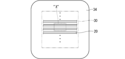
- FIG. 1 is a plan view schematically showing a top structure of an entire semiconductor device according to an embodiment
- FIG. 2 is an enlarged plan view of area "X" indicated in FIG. 1
- FIG. 3 is a cross-sectional view taken along line AA of FIG. 2
- FIG. 3 is a cross-sectional view taken along line BB of FIG. 2
- FIG. 3 is a cross-sectional view taken along line CC of FIG. 2
- FIG. 4 is a schematic diagram for explaining the effect produced by the trench gate type MOSFET of the present embodiment
- 3 is an equivalent circuit diagram of a transistor region
- FIG. 3 is an equivalent circuit diagram including a transistor region and a dummy region
- FIG. FIG. 9 is an equivalent circuit diagram when switching the trench gate type MOSFET at low speed in FIG.
- FIG. 9 is an equivalent circuit diagram when switching the trench gate type MOSFET at high speed in FIG.
- FIG. 3 is a modified example of a cross-sectional view taken along line CC of FIG. 2
- FIG. 11 is a plan view showing a modification of the configuration of the characterizing portion of a trench gate type MOSFET formed on a silicon carbide semiconductor substrate
- 13 is a cross-sectional view taken along line AA of FIG. 12
- FIG. FIG. 13 is a cross-sectional view taken along line BB of FIG. 12
- FIG. 13 is a cross-sectional view along line CC of FIG. 12
- 1 is a plan view schematically showing the configuration of a trench gate type MOSFET of this embodiment
- FIG. 1 is a plan view schematically showing the configuration of a trench gate type MOSFET of this embodiment
- FIG. 1 is a plan view schematically showing the configuration of a trench gate type MOSFET of this embodiment
- FIG. 1 is a cross-sectional view schematically showing the configuration of a trench gate type MOSFET of this embodiment
- FIG. 10 is a cross-sectional view schematically showing a modification of the configuration of the trench gate type MOSFET of the present embodiment
- FIG. 10 is a cross-sectional view schematically showing a modification of the configuration of the trench gate type MOSFET of the present embodiment
- 1 is a plan view schematically showing the configuration of a trench gate type MOSFET of this embodiment
- FIG. 10 is a plan view showing a modification of the configuration of the characterizing portion of a trench gate type MOSFET formed on a silicon carbide semiconductor substrate (SiC substrate); BRIEF DESCRIPTION OF THE DRAWINGS It is a block diagram which shows the structure of the power conversion system to which the power converter regarding embodiment is applied.
- FIG. 10 is a plan view showing a modification of the configuration of the characterizing portion of a trench gate type MOSFET formed on a silicon carbide semiconductor substrate (SiC substrate);
- MOS Metal-Oxide-Semiconductor
- MOS transistor a field effect transistor having a MOS structure
- polycrystalline silicon has been adopted as the material of the gate electrode instead of metal, mainly from the viewpoint of forming the source-drain in a self-aligned manner.
- a material with a high dielectric constant is employed as the material of the gate insulating film, but the material is not necessarily limited to oxide.
- MOS is not necessarily limited only to the stacked structure of metal/oxide/semiconductor, and this specification does not presuppose such a limitation.
- MOS here is not only an abbreviation derived from its etymology, but also broadly includes the layered structure of conductor/insulator/semiconductor.
- n-type is generally defined as “first conductivity type” and p-type as “second conductivity type” with respect to the conductivity type of impurities, but the definition may be reversed.
- FIG. 1 is a plan view schematically showing the top structure of the entire semiconductor device according to the present embodiment.
- the semiconductor device according to the present embodiment has a rectangular outer shape, and at the center thereof is a minimum unit structure of a MOSFET (MOSFET cell) called a "unit cell”.
- MOSFET cell MOSFET cell
- a plurality of active regions 30 are provided, and the outer sides of the active regions 30 are surrounded by termination regions 34 .
- a plurality of gate trenches 20 are provided in parallel at intervals in the active region 30 .
- the plurality of gate trenches 20 are connected to gate wiring provided in the active region 30, and the gate wiring is connected to a gate pad, but illustration and description of these are omitted.
- FIG. 2 is an enlarged plan view of area "X" shown in FIG.
- the characteristic configuration shown in the region "X" will be described as this embodiment and its modification, and FIG. 1 is common to each embodiment and its modification.
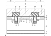
- FIG. 2 is a plan view showing an example of the configuration of the characteristic portion of the semiconductor device of the present embodiment, more specifically, a trench gate type MOSFET formed on a silicon carbide semiconductor substrate (SiC substrate).
- the trench gate type MOSFET according to the present embodiment includes two adjacent gate trenches 20 and respective impurity regions (connection layer 12 and second well region) provided therebetween. including the region 14) constitute one unit cell 31.
- FIG. 1 is shown in FIG. 2, the trench gate type MOSFET according to the present embodiment includes two adjacent gate trenches 20 and respective impurity regions (connection layer 12 and second well region) provided therebetween. including the region 14) constitute one unit cell 31.
- FIG. 1 the trench gate type MOSFET according to the present embodiment includes two adjacent gate trenches 20 and respective impurity regions (connection layer 12 and second well region) provided therebetween. including the region 14) constitute one unit cell 31.
- the gate trenches 20 are provided in stripes so as to extend in a direction parallel to the off direction of the silicon carbide semiconductor substrate, and divide the active regions 30 into MOSFET cell units.
- the inner wall of gate trench 20 is covered with gate insulating film 7 , and gate electrode 9 is embedded in the region surrounded by gate insulating film 7 .
- the active region 30 between the gate trenches 20 is provided with a first contact 6 and a second contact 16 penetrating through an interlayer insulating film (here, not shown).
- One or more first well contact regions 8 are provided on the bottom surface of the first contact 6
- a second well contact region 18 is provided on the bottom surface of the second contact 16 .
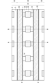
- FIG. 3 is a cross-sectional view along line AA in FIG.
- FIG. 4 is a cross-sectional view taken along line BB of FIG.
- FIG. 5 is a cross-sectional view taken along line CC of FIG. 3, 4 and 5 show the periodic structure of the unit cell 31 at a position including the gate trench 20 in cross section in the active region 30.
- FIG. 2 the configuration above the connection layer 12 in the drift layer 3 is omitted for the sake of convenience so that the arrangement of the connection layer 12 in the drift layer 3 can be understood.
- the trench gate MOSFET of the present embodiment includes n-type drift layer 3 provided on one main surface (first main surface) of silicon carbide semiconductor substrate 1 and , a gate trench 20 provided in the drift layer 3 extending in the first direction (the depth direction of the paper surface in FIG. 3), and a p-type trench 20 provided in the upper layer portion of the drift layer 3 and extending in the first direction.
- First contact 6 electrically connected to electrode 10 is separated by gate trench 20 in a second direction (a direction along the first main surface of silicon carbide semiconductor substrate 1) orthogonal to the first direction.
- a p-type second well region 14 extending in the first direction and having no n-type impurity region therein; , a p-type second well contact region 18, and a second contact electrically connected to the second well contact region 18 and electrically connected to the source electrode 10 provided above the drift layer 3.
- p-type electric field relaxation region 13 provided in contact with the bottom of gate trench 20, and a second direction (silicon carbide semiconductor provided in the drift layer 3 so as to be in contact with the sidewall of at least one of the gate trenches 20 in the direction along the first main surface of the substrate 1, and the electric field relaxation regions 13 and the second well regions 14 It has a p-type connection layer 12 for electrical connection and a drain electrode 11 provided below the drift layer 3 .
- a gate electrode 9 is provided via the film 7 .
- An interlayer insulating film 19 is provided so as to cover the gate trenches 20 and their surroundings. contacts 16 (contact openings) are respectively formed. The bottom surfaces of the first contact 6 and the second contact 16 are covered with a silicide film 17 , and the source electrode 10 is connected to the first contact 6 and the second contact 16 .
- silicon carbide semiconductor substrate 1 has a polytype of 4H, and the main surface of silicon carbide semiconductor substrate 1 and the main surface of drift layer 3 have an off angle ⁇ inclined in the [11-20] axial direction ( 0001) plane.
- the off angle ⁇ may be, for example, 10° or less.
- the first well region 4 in the upper layer portion of the drift layer 3 is provided in an active region 30 in which MOSFET cells are arranged, and selectively (partially) in the first well region 4, the first A source region 5 and a first well contact region 8 are provided.
- the first well contact region 8 is surrounded by the first source region 5 in plan view, as shown in FIG.
- the second well region 14 in the upper layer portion of the drift layer 3 is provided within the active region 30 in which the MOSFET cells are arranged.
- a well contact region 18 is provided.
- the second well contact region 18 is surrounded by the second well region 14 in plan view as shown in FIG.
- a gate electrode 9 is embedded in the gate trench 20 with the gate insulating film 7 interposed therebetween, and the top surface of the gate electrode 9 is located deeper than the outermost surface of the first source region 5 . That is, the upper surface of gate electrode 9 is located at a position recessed from the opening end of gate trench 20 . This is the same for the cross section taken along line BB, an example of which is shown in FIG.
- the electric field relaxation region 13 provided under the bottom surface of the gate trench 20 is provided for relaxing the electric field applied to the bottom surface and side surfaces of the gate trench 20 when the MOSFET is turned off, and is preferably in contact with the gate trench 20. .
- connection layer 12 provided so as to be in contact with the side surface of the electric field relaxation region 13 and part of the side wall of the gate trench 20 is also in contact with the second well region 14 so as to separate the electric field relaxation region 13 and the second well region 14 . It plays a role of electrically connecting with the well region 14 .
- a region including the second well region 14 is a dummy region 33 and a region other than the dummy region 33 that functions as a transistor is a transistor region 32 .
- connection layer 12 only contacts part of the sidewalls of the gate trenches 20, in FIG. It is provided continuously or discontinuously only on the side wall on the side in contact with 14 .
- An inversion channel is formed on the side wall of the gate trench 20 on the side contacting the first well region 4 under gate bias, and functions as a channel region of the MOSFET. At this time, the channel characteristics of each side wall of the gate trench 20 are substantially the same and are configured so as not to be non-uniform.
- the drift layer 3 has an off-angle in the ⁇ 11-20> direction, it is not affected by the anisotropy of the electrical characteristics caused by the difference in the crystal plane between the side walls of the gate trench 20. Identical and uniform channel characteristics can be achieved.
- the gate trench 20 penetrates the first source region 5 , the n-type first source region 5 is formed in the portion corresponding to the corner of the opening end of the gate trench 20 .
- the upper surface of the gate electrode 9 recedes from the opening end of the gate trench 20 at the corners of the opening end of the gate trench 20 , so that the first source region 5 and the gate electrode 9 do not face each other with the gate insulating film 7 interposed therebetween.
- the active region 30 as a whole does not have to have the planar configuration and cross-sectional configuration illustrated in FIGS. It may be Moreover, there is no limit to the ratio of the cross-sectional configurations shown in FIGS. 3 to 5, and configurations such as a configuration in which one side is large and the other side is small can be freely set.
- FIG. 23 is a modification of the cross-sectional view taken along line AA in FIG. As shown in FIG. 23, the first well contact region 8A and the second well contact region 18A are formed on the entire bottom surfaces of the first contact 6 and the second contact 16, respectively. I don't mind.
- FIG. 11 is a modified example of a cross-sectional view taken along line CC of FIG. As an example is shown in FIG. 11, a region in which the second contact 16 is not formed may be provided in the direction in which the gate trench 20 extends.
- the impurity concentration (cm ⁇ 3 ) indicates the peak value of the impurity concentration in the respective impurity layers and impurity regions.
- Nitrogen (N) or phosphorus (P) may be used as the n-type impurity, and aluminum (Al) or boron (B) may be used as the p-type impurity.
- n-type silicon carbide semiconductor substrate 1 in a wafer state having a polytype of 4H First, on one main surface of n-type silicon carbide semiconductor substrate 1 in a wafer state having a polytype of 4H, relatively high-resistance carbonization having a relatively low n-type impurity concentration (n ⁇ ) is formed.
- a drift layer 3 of silicon is formed by epitaxial growth. At this time, the drift layer 3 is formed so that the impurity concentration thereof is 1 ⁇ 10 14 cm ⁇ 3 or more and 1 ⁇ 10 17 cm ⁇ 3 or less.
- RIE reactive ion etching
- photolithography is performed with reference to the alignment marks formed on the dicing lines
- an ion implantation mask is formed on the drift layer 3, and the ion implantation is performed.
- Impurity ion implantation is performed through a mask.
- a p-type first well region 4 and a p-type second well region 14 are formed in the upper layer portion of the drift layer 3, and furthermore, the upper layer portion of the p-type first well region 4 is formed.
- a first source region 5 having a relatively low resistance and having a relatively high n-type impurity concentration (n + ) is formed in the region.
- the ion implantation mask for example, a resist mask or the like is used.
- first source region 5 has an impurity concentration of, for example, 5 ⁇ 10 18 cm ⁇ 3 or more and 5 ⁇ 10 20 cm ⁇ 3 or less
- first well region 4 and second well region 4 have an impurity concentration of 5 ⁇ 10 20 cm ⁇ 3 or less.
- Region 14 is formed to have an impurity concentration of, for example, 1 ⁇ 10 16 cm ⁇ 3 or more and 3 ⁇ 10 19 cm ⁇ 3 or less.
- the n-type impurity concentration of the first source region 5 is equal to that of the first well region 4 is set higher than the p-type impurity concentration of .
- the concentration in the first well region 4 and the second well region 14 may or may not be constant in the depth direction.
- the distribution may be such that the surface concentration is low, or the distribution may be such that it has a peak in the depth direction.
- a p-type first well contact region 8 is formed in the first source region 5, and a p-type second well contact region 18 is formed in the second well region 14 by ion implantation.
- the first well contact region 8 and the second well contact region 18 have a p-type impurity concentration of, for example, 1 ⁇ 10 19 cm ⁇ 3 or more and 1 ⁇ 10 22 cm ⁇ 3 or less. to form.
- the thickness of the first well contact region 8 is formed to be equal to or greater than the thickness of the first source region 5, so that the first well contact region 8 becomes the first well. Ensure contact with area 4.
- the formation order of impurity layers and impurity regions formed in drift layer 3 is not limited to the case described in the present embodiment.
- an etching mask having openings corresponding to the forming regions of the gate trenches 20 on the drift layer 3 is patterned.
- the alignment marks may be used as a reference.
- a gate trench 20 is formed through the first source region 5, the first well region 4 and the second well region 14 in the thickness direction and reaching the drift layer 3 by RIE using an etching mask. .
- electric field relaxation region 13 has an impurity concentration of, for example, 1 ⁇ 10 17 cm ⁇ 3 or more and 1 ⁇ 10 20 cm ⁇ 3 or less.
- the ion implantation mask is patterned using a resist material.
- the ion implantation mask has a pattern in which openings are provided only in portions of the gate trenches 20 that include the side walls where the connection layer 12 is provided, and openings are provided in portions including the side walls where the connection layer 12 is not provided. Not provided.
- connection layer 12 is performed by tilting silicon carbide semiconductor substrate 1 in the wafer state. and 60 degrees or less, the impurity concentration is, for example, 5 ⁇ 10 16 cm ⁇ 3 or more and 1 ⁇ 10 20 cm ⁇ 3 or less, and the depth from the surface is 0.3 ⁇ m or more. .
- connection layer 12 is formed after the electric field relaxation region 13 is formed.
- the gate trench 20 may be formed in accordance with the formation positions of the electric field relaxation region 13 and the connection layer 12 .
- the ion implantation mask used for the ion implantation of the electric field relaxation region 13 for the formation of the gate trench 20 .
- the ion implantation for forming the connection layer 12 may be performed perpendicularly to the wafer.
- annealing for activating the implanted ions is performed at a temperature range of 1500° C. or more and 2200° C. or less for a time of 0.5 minutes or more and 60 minutes or less.
- a field insulating film (not shown here) is formed.
- the gate insulating film 7 is formed to cover the inner wall surface of the gate trench 20 and the periphery of the gate trench 20 by thermal oxidation, CVD, or the like.
- a conductor layer such as polysilicon containing a relatively high concentration of impurities is formed by CVD or the like.
- the polysilicon not only grows vertically from the bottom surface of the gate trench 20 but also grows horizontally from the side surface of the gate trench 20 .
- Polysilicon is relatively easily buried inside.
- the polysilicon on the drift layer 3 is removed by etching.
- the polysilicon formed on the surface of the drift layer 3 is removed by etching, but the polysilicon buried inside the gate trench 20 remains because of its large film thickness, and constitutes the gate electrode 9 .
- the upper surface of gate electrode 9 inside trench 20 is formed at a position recessed from the open end of gate trench 20 .
- the interlayer insulating film 19 After forming the interlayer insulating film 19 so as to cover the termination region 34 (see FIG. 1) and the active region 30 , formation regions of the first contact 6 and the second contact 16 are formed on the interlayer insulating film 19 .
- a resist material is used to pattern an etching mask having openings in portions corresponding to . When forming this etching mask, the alignment marks may be used as a reference.
- the interlayer insulating film 19 is formed to cover the termination region 34 (see FIG. 1) and the active region 30, the entire surface of the active region 30 is dry-etched to form the first contact 6 and the second contact. Contacts 16 may be formed.
- the interlayer insulating film 19 formed on the surface of the drift layer 3 is removed by etching. , and maintains the function of electrically insulating the gate electrode 9 and the source electrode 10 .
- the etching mask may be provided with an opening for forming a gate contact (here, not shown) formed in the termination region 34 (see FIG. 1).
- a gate contact here, not shown
- the interlayer insulating film 19 may be removed and the gate contact may be formed at the same time.
- the first contact 6, the second contact 16 and the gate contact may be formed in separate steps.
- a metal film such as nickel is formed by a sputtering method or the like so as to cover the first contact 6, the second contact 16 and the interlayer insulating film 19.
- a metal film such as nickel is formed by a sputtering method or the like so as to cover the first contact 6, the second contact 16 and the interlayer insulating film 19.
- FIG. After that, for example, by performing annealing at 300° C. or more and 1200° C. or less, the first source region 5 and the first well contact exposed at the bottom surface of the first contact 6 and the bottom surface of the second contact 16 are exposed.
- a metal silicide film (here, NiSi 2 film) is formed over the region 8 and the second well contact region 18 to form a silicide film 17 to form an ohmic contact.
- the ohmic contact is not formed and the Schottky contact is formed.
- the source electrode 10 is formed by a sputtering method or the like so as to bury the first contact 6 and the second contact 16, and the source electrode 10 is formed in the first source region 5, the first well contact region 8 and the second well contact region 8. It is electrically connected to well contact region 18 .
- a cross-sectional configuration examples of which are shown in FIGS. 3 and 4, can be obtained.
- a gate pad or a wiring for connection to the gate pad is formed from the inside of the gate contact (not shown) to the upper portion.
- the drain electrode 11 is formed on the other main surface of the silicon carbide semiconductor substrate 1 by sputtering or the like, thereby obtaining the trench gate type MOSFET whose examples are shown in FIGS.
- connection layer 12 contacts one side surface of the electric field relaxation region 13 .
- Connection layer 12 also contacts second well region 14 . Therefore, electric field relaxation region 13 is electrically connected to second well region 14 .
- connection layer 12 secures a current path for a displacement current that flows as the depletion layer formed in the pn junction expands and contracts.
- the electric field relaxation region 13 When the connection layer 12 is not provided, the electric field relaxation region 13 has a floating potential, so that the potential follow-up of the electric field relaxation region 13 to the ON/OFF operation of the MOSFET becomes slow. As a result, the response speed of the depletion layer formed by the pn junction becomes slow, resulting in a structure that is difficult to turn off and turn on. As a result, switching loss increases.
- connection layer 12 By providing the connection layer 12, the response speed of the depletion layer formed by the pn junction can be increased, and switching loss can be reduced.
- connection layer 12 Since the connection layer 12 is formed only on the sidewall of the gate trench 20 on the side contacting the second well region 14, the channel density does not decrease, and the on-resistance increases due to the provision of the connection layer 12. can be suppressed. In addition, uniform channel characteristics can be realized by making the trench side wall where the connection layer 12 is not formed to be the trench side wall extending in the direction parallel to the off-direction. As a result, concentration of current on a specific channel surface is suppressed, and a MOSFET with high operational stability can be realized without instability of the threshold voltage.
- connection layer 12 is formed only on the sidewall of the gate trench 20 on the side contacting the second well region 14 , the first well region 4 and the electric field relaxation region 13 are electrically separated in the active region 30 . not properly connected. In other words, the first well region 4 and the second well region 14 are not electrically connected in the active region 30 . That is, current for charging/discharging the pn junction formed by electric field relaxation region 13 and drift layer 3 mainly flows through second well region 14 . Therefore, it is possible to suppress the potential fluctuation occurring in the first well region 4 during the switching operation, and it is possible to realize a MOSFET with high operational stability.
- the first well region 4 and the second well region 14 may be electrically connected in the termination region 34, and this does not limit the effect of realizing a MOSFET with high operational stability. .
- FIG. 6 is a schematic diagram for explaining the effect produced by the trench gate type MOSFET of this embodiment.
- FIG. 7 is an equivalent circuit diagram of the transistor region 32. As shown in FIG. In FIG. 7, illustration of the contact resistance ⁇ a is omitted for the sake of convenience.
- FIG. 8 is an equivalent circuit diagram combining the transistor region 32 and the dummy region 33. As shown in FIG. In FIG. 8, contact resistances ⁇ a and ⁇ b are omitted for convenience.
- Cgs is the capacitance between the gate electrode 9 and the source electrode 10 (hereinafter referred to as gate-source capacitance), and Cgd is the capacitance between the gate electrode 9 and the drain electrode 11 (hereinafter referred to as gate-drain capacitance).
- Cds is the capacitance between the drain electrode 11 and the source electrode 10 (hereinafter referred to as drain-source capacitance)
- Cgp is the capacitance between the gate electrode 9 and the second well region 14 (hereinafter referred to as , gate-well capacitance)
- Cdp is the capacitance between the drain electrode 11 and the second well region 14 (hereinafter referred to as drain-well capacitance).
- Rp is the resistance component of the connection layer 12, the electric field relaxation region 13 and the second well region 14; contact resistance.
- a region including the second well region 14 is a dummy region 33 and a region other than the dummy region 33 that functions as a transistor is a transistor region 32 .
- FIG. 9 is an equivalent circuit diagram when switching the trench gate type MOSFET at low speed in FIG. In FIG. 9, gate-well capacitance Cgp is removed from the circuit diagram shown in FIG.
- a displacement current is generated in the electric field relaxation region 13 and the second well region 14 due to charging and discharging of the drain-well capacitance Cdp. Since the impedance is sufficiently large, the displacement current mainly flows to the source electrode 10 via the resistance component Rp.
- FIG. 10 is an equivalent circuit diagram when switching the trench gate type MOSFET at high speed in FIG.
- resistance component Rp of electric field relaxation region 13 and second well region 14 is removed from the circuit diagram shown in FIG.
- a displacement current is generated in the electric field relaxation region 13 and the second well region 14 due to charging and discharging of the drain-well capacitance Cdp. Since the impedance is sufficiently smaller than Rp, the displacement current mainly flows to the gate electrode 9 via the gate-well capacitance Cgp.
- the effective capacitive coupling between the drain electrode 11 and the gate electrode 9 becomes larger than in the case of low-speed switching.
- connection layer 12 extends from the sidewall of the gate trench 20 in a direction (second direction, left-right direction in FIG. 3) perpendicular to the extending direction of the gate trench 20 (first direction, left-right direction in FIG. 2). provided to exist.
- Drift layer 3 between adjacent gate trenches 20 may be blocked by two opposing connection layers 12, but in order to increase the pn junction capacitance formed by connection layer 12 and drift layer 3, drift More preferably, layer 3 is not interrupted.
- connection layers 12 are provided separated from each other along the extending direction of the gate trenches 20 (the first direction, the horizontal direction in FIG. 2), and an example is shown in FIG. As shown, the connecting layer 12 may be provided continuously in the first direction.
- FIG. 24 is a plan view showing a modification of the configuration of the characterizing portion of a trench gate type MOSFET formed on a silicon carbide semiconductor substrate (SiC substrate).
- connection layer 12A is provided continuously along the direction in which the gate trench 20 extends.
- FIG. 26 is a plan view showing a modification of the configuration of the characterizing portion of a trench gate type MOSFET formed on a silicon carbide semiconductor substrate (SiC substrate). 26 are the same as those in FIGS. 3 and 4, respectively.
- the first well contact region 8 and the second well contact region 18 are discontinuously formed in the extending direction of the gate trench 20, but in FIG.
- Well contact region 8B and second well contact region 18B are formed continuously in the direction in which gate trench 20 extends. Even when such a configuration is adopted, it is possible to suppress an increase in switching loss and reduce electromagnetic noise.
- FIG. 12 is a plan view showing a modification of the configuration of the characterizing portion of a trench gate type MOSFET formed on a silicon carbide semiconductor substrate (SiC substrate).
- FIG. 13 is a cross-sectional view along line AA in FIG. 14 is a cross-sectional view taken along line BB of FIG. 12.
- FIG. 15 is a cross-sectional view taken along line CC of FIG. 12.
- FIG. 13, 14 and 15 show the periodic structure of the unit cell 31 at a position including the gate trench 20 in cross section in the active region 30.
- the second well region 14 was provided with the second well contact region 18, but in the configuration shown in FIG. 2 of the well contact region 18, an n-type second source region 15 having a smaller area than the first source region 5 in plan view is provided.
- a second source region 15 is provided in the upper layer portion of the second well region 14 and contacts the side surface of the second well contact region 18 .
- the n-type impurity concentration of the second source region 15 should be, for example, 5 ⁇ 10 18 cm ⁇ 3 or more and 5 ⁇ 10 20 cm ⁇ 3 or less, like the first source region 5. is preferred.
- FIG. 16 is a plan view schematically showing the configuration of the trench gate type MOSFET of this embodiment.
- the n-type second source region 15 extends in the extending direction of the gate trench 20 (first direction, right and left in FIG. 16). direction) (second direction, left-right direction in FIG. 3), the connection layer 12 or the second well contact region 18 are not flush with each other. That is, the second source region 15 is not located in the cross section taken along line AA in FIG. Similarly, the second source region 15 is not located in the cross section taken along line BB of FIG.
- FIG. 17 is a plan view schematically showing the configuration of the trench gate type MOSFET of this embodiment.
- the p-type second well contact region 18C has a larger area in plan view than the first well contact region 8. is small.
- ⁇ b can be increased, and effective capacitive coupling between the drain electrode 11 and the gate electrode 9 can be increased in the high frequency region. Therefore, the effect of reducing electromagnetic noise can be enhanced.
- FIG. 18 is a plan view schematically showing the configuration of the trench gate type MOSFET of this embodiment.
- a direction second , the left-right direction in FIG. 3
- the connection layer 12 and the second well contact region 18 are not located on the same plane.
- the connection layer 12 is located and the second well contact region 18 is not located.
- the second well contact region 18 is located and the connection layer 12 is not located in the cross section along line BB in FIG.
- the resistance component Rp can be increased, and the effective capacitive coupling between the drain electrode 11 and the gate electrode 9 can be increased in the high frequency region. Therefore, the effect of reducing electromagnetic noise can be enhanced.
- the impurity concentration of the second well region 14 forming the dummy region 33 in FIG. 3 is equal to the impurity concentration of the first well region 4 forming the transistor region 32 in FIG. lower than
- the resistance component Rp of the second well region 14 can be increased, and the effective capacitive coupling between the drain electrode 11 and the gate electrode 9 can be increased in the high frequency region. Therefore, the effect of reducing electromagnetic noise can be enhanced.
- the impurity concentration of the second well region 14 may be even slightly lower than the impurity concentration of the first well region 4.
- the effect can be obtained by reducing the impurity concentration by several percent to several tens of percent.
- the length of the two well regions 14 is formed smaller than the width of the first well region 4 (in that direction) that constitutes the transistor region 32 in FIG.
- the resistance component Rp of the second well region 14 can be increased, and the effective capacitive coupling between the drain electrode 11 and the gate electrode 9 can be increased in the high frequency region. Therefore, the effect of reducing electromagnetic noise can be enhanced.
- the width of the second well region 14 may be made even slightly smaller than the width of the first well region 4. For example, the effect can be obtained by reducing the width by several percent to several tens of percent.
- FIG. 19 is a cross-sectional view schematically showing the structure of the trench gate type MOSFET of this embodiment. The corresponding plan view is similar to FIG.
- the impurity concentration of the high-concentration region 21 is preferably lower than the p-type impurity concentration of the connection layer 12 , the electric field relaxation region 13 and the second well region 14 .
- the impurity concentration of the high-concentration region 21 is set higher than that of the drift layer 3 .
- the drain-well capacitance Cdp can be increased, and the effective capacitive coupling between the drain electrode 11 and the gate electrode 9 can be increased in the high frequency region. Therefore, the effect of reducing electromagnetic noise can be enhanced.
- FIG. 20 is a cross-sectional view schematically showing a modification of the configuration of the trench gate type MOSFET of this embodiment. The corresponding plan view is similar to FIG.
- the high concentration region 21A is provided not only directly below the second well region 14 but also directly below the first well region 4. As shown in FIG. 20, in the trench gate type MOSFET, the high concentration region 21A is provided not only directly below the second well region 14 but also directly below the first well region 4. As shown in FIG. 20, in the trench gate type MOSFET, the high concentration region 21A is provided not only directly below the second well region 14 but also directly below the first well region 4. As shown in FIG. 20, in the trench gate type MOSFET, the high concentration region 21A is provided not only directly below the second well region 14 but also directly below the first well region 4. As shown in FIG.
- the impurity concentration of the high-concentration region 21A is preferably lower than that of the first well region 4. This is because the depletion layers formed by the pn junctions formed between the high-concentration region 21A and the first well region 4 and between the high-concentration region 21A and the electric field relaxation region 13 are shifted toward the high-concentration region 21A side. This is for stretching.
- the impurity concentration of the high-concentration region 21A is made higher than that of the drift layer 3.
- FIG. 21 is a cross-sectional view schematically showing a modification of the configuration of the trench gate type MOSFET of this embodiment. The corresponding plan view is similar to FIG.
- the high-concentration region 21 as shown in FIG. 21 is formed by forming the gate trench 20, removing the etching mask, and implanting n-type impurity ions from an oblique direction to form the side wall of the gate trench 20 and the electric field. It is formed in contact with the relaxation region 13 .
- the high concentration region 21 is formed directly under the second well region 14 or directly under the first well region 4 and directly under the second well region 14 . The effects produced by this configuration are similar to those produced by the configurations shown in FIGS.
- FIG. 22 is a plan view schematically showing the configuration of the trench gate type MOSFET of this embodiment.
- the first source regions 5 are discontinuously formed in the extending direction of the first well region 4 .
- the impurity concentrations of the p-type impurities in the first well contact region 8 and the second well contact region 18 are the same.
- the contact resistivity ( ⁇ cm 2 ) is also the same, for example, the opening area of the second contact 16 above the second well contact region 18 is the same as that of the first well contact region 8 of the first contact 6 .
- the contact resistance ⁇ a to the second well contact region 18 can be made larger than the contact resistance ⁇ b to the first well contact region 8 .
- the contact resistance .rho it can be made larger than the contact resistance ⁇ b for the contact region 8 .
- the contact resistance ⁇ b (see FIG. 6) with respect to the second well contact region 18 can be increased, and the effective capacitive coupling between the drain electrode 11 and the gate electrode 9 can be increased in the high frequency region. can be done. Therefore, the effect of reducing electromagnetic noise can be enhanced.
- the first well contact region 8 and the second well contact region 18 have the same p-type impurity concentration, and the contact resistivity ( ⁇ cm 2 ) is , the contact resistivity for the second well contact region 18 can also be formed to be greater than the contact resistivity for the first well contact region 8 .
- the above can be realized by setting the impurity concentration of the p-type impurities on the outermost surface of the second well contact region 18 to be lower than the impurity concentration of the p-type impurities on the outermost surface of the first well contact region 8. be.
- the contact resistance ⁇ b (FIG. 6) with respect to the second well contact region 18 can be increased, and the effective capacitive coupling between the drain electrode 11 and the gate electrode 9 can be increased in the high frequency region. . Therefore, the effect of reducing electromagnetic noise can be enhanced.
- the semiconductor devices according to the first to eighth embodiments are applied to a power converter.
- the present embodiment is not limited to application to a specific power converter, a case where the semiconductor device described above is applied to a three-phase inverter will be described below as a ninth embodiment.
- FIG. 25 is a block diagram showing the configuration of a power conversion system to which the power conversion device according to this embodiment is applied.
- the power conversion system shown in FIG. 25 includes a power supply 500, a power conversion device 600, and a load 700.
- the power supply 500 is a DC power supply and supplies DC power to the power conversion device 600 .
- the power supply 500 can be configured with various devices, for example, it can be configured with a DC system, a solar battery, or a storage battery, or it can be configured with a rectifier circuit or an AC/DC converter connected to an AC system. may Also, power supply 500 may be configured by a DC/DC converter that converts DC power output from a DC system into predetermined power.
- the power conversion device 600 is a three-phase inverter connected between the power supply 500 and the load 700 , converts the DC power supplied from the power supply 500 into AC power, and supplies the AC power to the load 700 . As shown in FIG. 25, the power conversion device 600 outputs a main conversion circuit 601 that converts DC power into AC power and outputs a drive signal that drives the switching elements of the main conversion circuit 601. A drive circuit 602 and a control circuit 603 that outputs a control signal for controlling the drive circuit 602 to the drive circuit 602 are provided.
- a load 700 is a three-phase electric motor driven by AC power supplied from the power converter 600 .
- the load 700 is not limited to a specific application, and is an electric motor mounted on various electrical equipment, such as a hybrid vehicle, an electric vehicle, a railroad vehicle, an elevator, or an electric motor for air conditioning equipment.
- the main conversion circuit 601 includes a switching element and a freewheeling diode (here, not shown). By switching the switching element, the DC power supplied from the power supply 500 is converted into AC power and supplied to the load 700. do.
- the main conversion circuit 601 has various specific circuit configurations, the main conversion circuit 601 according to the present embodiment is a two-level three-phase full bridge circuit, and has six switching elements and an inverse switching element for each switching element. It can consist of six freewheeling diodes in parallel.
- the semiconductor device according to any one of the first to eighth embodiments is applied to each switching element of the main conversion circuit 601 .
- the six switching elements are connected in series every two switching elements to form upper and lower arms, and the respective upper and lower arms form respective phases (U phase, V phase, W phase) of the full bridge circuit.
- Output terminals of the respective upper and lower arms, that is, three output terminals of the main conversion circuit 601 are connected to the load 700 .
- the drive circuit 602 generates a drive signal for driving the switching element of the main conversion circuit 601 and supplies it to the control electrode of the switching element of the main conversion circuit 601 .
- a drive signal for turning on a switching element and a drive signal for turning off a switching element are output to control electrodes of the respective switching elements.
- the driving signal When maintaining the switching element in the ON state, the driving signal is a voltage signal (ON signal) equal to or higher than the threshold voltage of the switching element, and when maintaining the switching element in the OFF state, the driving signal is equal to the threshold voltage of the switching element. It becomes a voltage signal (OFF signal) below the voltage.
- the control circuit 603 controls the switching elements of the main conversion circuit 601 so that the desired power is supplied to the load 700 . Specifically, based on the power to be supplied to the load 700, the time (on time) during which each switching element of the main conversion circuit 601 should be in the ON state is calculated. For example, the main conversion circuit 601 can be controlled by PWM control that modulates the ON time of the switching element according to the voltage to be output. Then, a control command (control signal) is output to the drive circuit 602 so that an ON signal is output to the switching element that should be in the ON state at each time point, and an OFF signal is output to the switching element that should be in the OFF state. The drive circuit 602 outputs an ON signal or an OFF signal as a drive signal to the control electrode of each switching element according to this control signal.
- the semiconductor device according to any one of the first to eighth embodiments is applied as the switching element of the main conversion circuit 601
- An electric field applied to the bottom surface of the gate trench can be relaxed.
- the electric field relaxation region 13 at the bottom of the trench and the first well region 4 are electrically connected by the connection layer 12, the pn junction formed by the electric field relaxation region 13 at the bottom of the trench and the drift layer 3 is filled. A current path for discharging is secured, and switching loss can be reduced.
- the application is not limited to this, and can be applied to various power converters.
- a two-level power converter is used, but a three-level or multi-level power converter may be used.
- when power is supplied to a single-phase load it may be applied to a single-phase inverter.
- when power is supplied to a DC load or the like it can be applied to a DC/DC converter or an AC/DC converter.
- the power conversion device to which the above semiconductor device is applied is not limited to the case where the above load is an electric motor. It can also be used as a power supply device for a solar power generation system or a power storage system.
- the replacement may be made across multiple embodiments. In other words, it may be the case that the respective configurations whose examples are shown in the different embodiments are combined to produce the same effect.
- the semiconductor device includes a first semiconductor layer of a first conductivity type, a gate trench 20 and a first well region 4 of a second conductivity type (p-type). , a first impurity region of the first conductivity type, and at least one first well contact region 8 of the second conductivity type (p-type) (or the first well contact region 8A, the first well contact region 8A). contact region 8B), at least one first contact 6, a second well region 14 of the second conductivity type (p-type), and at least one second well region 14 of the second conductivity type (p-type).
- Well contact region 18 (or second well contact region 18A, second well contact region 18B, second well contact region 18C), at least one second contact 16, and a second conductivity type (p type) electric field relaxation region 13, a plurality of connection layers 12 (or connection layers 12A) of the second conductivity type (p-type), and a second main electrode.
- the first conductivity type first semiconductor layer corresponds to, for example, the n-type drift layer 3 or the like.
- the first impurity region of the first conductivity type corresponds to, for example, the n-type first source region 5 or the like.
- the second main electrode corresponds to, for example, the drain electrode 11 and the like.
- Gate trench 20 is provided on the upper surface of drift layer 3 to extend in a first direction along the upper surface of drift layer 3 (that is, the depth direction in FIG. 3).
- the first well region 4 is provided in the upper layer portion of the drift layer 3 and extends in the first direction.
- a first source region 5 is provided in an upper layer portion of the first well region 4 .
- a first well contact region 8 is provided in the upper layer of the first well region 4 and contacts the first source region 5 on the side surface.
- a first contact 6 is electrically connected to the first source region 5 and the at least one first well contact region 8 and electrically to a first main electrode provided above the drift layer 3 .
- the first main electrode corresponds to, for example, the source electrode 10 or the like.
- the second well regions 14 are separated by the gate trenches 20 in a second direction (that is, the horizontal direction in FIG. 3) along the upper surface of the drift layer 3 and perpendicular to the first direction, and , extending in the first direction and having no impurity region of the first conductivity type therein.
- a second well contact region 18 is provided in an upper layer portion of the second well region 14 .
- the second contact 16 is electrically connected to the second well contact region 18 and electrically connected to the source electrode 10 provided above the drift layer 3 .
- Electric field relaxation region 13 is provided in contact with the bottom of gate trench 20 .
- connection layer 12 is provided in contact with mutually opposing sidewalls (sidewalls in contact with the second well region 14 ) of the adjacent gate trenches 20 , and separates the electric field relaxation region 13 and the second well region 14 . Connect electrically. Drain electrode 11 is provided below drift layer 3 . Inside the gate trench 20, a gate insulating film is formed on the side surface of the first source region 5, the side surface of the first well region 4, the side surface of the second well region 14, the electric field relaxation region 13, and the connection layer 12. A gate electrode 9 is provided via 7 .
- the semiconductor device includes the drift layer 3, the gate trench 20, the first well region 4, the first source region 5, and the first well contact region. 8, a first contact 6, a second well region 14, a second well contact region 18, at least one second impurity region of the first conductivity type (n-type), and a second A contact 16 , an electric field relaxation region 13 , a connection layer 12 and a drain electrode 11 are provided.
- the second impurity region corresponds to, for example, the n-type second source region 15 or the like.
- the second well region 14 is provided separated by the gate trench 20 in a second direction along the upper surface of the drift layer 3, which is a direction orthogonal to the first direction, and extends in the first direction. .
- the second source region 15 is provided in the upper layer portion of the second well region 14, is in contact with the side surface of at least one second well contact region 18, and has an area of the first source region in plan view. less than 5. Also, the connection layer 12 is not provided on the side wall that contacts the first well region 4 . Inside the gate trench 20, a gate insulating film is formed on the side surface of the first source region 5, the side surface of the first well region 4, the side surface of the second well region 14, the electric field relaxation region 13, and the connection layer 12. A gate electrode 9 is provided via 7 .
- the effect of reducing the on-resistance can be obtained. Further, by providing the n-type second source region 15, even if the MOSFET is partially formed in the second well region 14, the region where the MOSFET exists in the first well region 4 and the second If there is a gate-well capacitance Cgp in the portion where the n-type region is not formed in the second well region 14 with respect to the sum of the region where the MOSFET is partially formed in the well region 14 of the second well region 14, The effect of reducing electromagnetic noise can be obtained in the same manner as the configuration in which the n-type region is not formed in the second well region 14 .
- the second source region 15 is not formed coplanar with the connection layer 12 or the second well contact region 18 in the second direction. According to such a configuration, it is possible to effectively reduce the on-resistance of the trench gate type MOSFET.
- the second well contact region 18C has a smaller area than the first well contact region 8 in plan view.
- the second well contact region 18 and the connection layer 12 are not formed on the same plane in the second direction.
- the resistance component Rp can be increased, and the effective capacitive coupling between the drain electrode 11 and the gate electrode 9 can be increased in the high frequency region. Therefore, the effect of reducing electromagnetic noise can be enhanced.
- the second well region 14 has a lower impurity concentration than the first well region 4 .
- the resistance component Rp of the second well region 14 can be increased, and the effective capacitive coupling between the drain electrode 11 and the gate electrode 9 can be increased in the high frequency region. . Therefore, the effect of reducing electromagnetic noise can be enhanced.
- the length of the second well region 14 in the second direction is shorter than the length of the first well region 4 in the second direction.
- the resistance component Rp of the second well region 14 can be increased, and the effective capacitive coupling between the drain electrode 11 and the gate electrode 9 can be increased in the high frequency region. . Therefore, the effect of reducing electromagnetic noise can be enhanced.
- the semiconductor device is provided below the second well region 14 and has a first conductivity type high concentration region having a higher impurity concentration than the drift layer 3 . 21 (or high concentration region 21A).
- the drain-well capacitance Cdp can be increased, and effective capacitive coupling between the drain electrode 11 and the gate electrode 9 can be increased in a high frequency region. Therefore, the effect of reducing electromagnetic noise can be enhanced.
- the high-concentration region 21A is also provided below the first well region 4 .
- the effect of reducing the on-resistance can be obtained.
- the first source regions 5 are formed discontinuously in the first direction. According to such a configuration, it is possible to arbitrarily set the trade-off relationship between the on-characteristics of the MOSFET and the withstand voltage. That is, by providing the portion where the first source region 5 is not formed, the voltage resistance can be improved, and by providing the portion where the first source region 5 is formed, the on-characteristics of the MOSFET can be improved. . Therefore, by adjusting the ratio of the portion where the first source region 5 is not formed and the portion where the first source region 5 is formed, it is possible to arbitrarily set the trade-off relationship between the on-characteristics of the MOSFET and the withstand voltage. can be done.
- the contact resistance of the at least one second contact 16 to the at least one second well contact region 18 is less than that of the at least one first contact 6 . greater than the contact resistance to the first well contact region 8.
- the contact resistance ⁇ b (FIG. 6) with respect to the second well contact region 18 can be increased, and the effective capacitive coupling between the drain electrode 11 and the gate electrode 9 can be improved in the high frequency region. can be increased. Therefore, the effect of reducing electromagnetic noise can be enhanced.
- the impurity concentration of at least one second well contact region 18 is lower than the impurity concentration of at least one first well contact region 8 .
- the contact resistance ⁇ b (FIG. 6) with respect to the second well contact region 18 can be increased, and the effective capacitive coupling between the drain electrode 11 and the gate electrode 9 can be improved in the high frequency region. can be increased. Therefore, the effect of reducing electromagnetic noise can be enhanced.
- the opening area of the at least one second contact 16 above the at least one second well contact region 18 is at least 100% of the at least one first contact 6 . smaller than the opening area on one first well contact region 8 .
- the material when a material name is described without being specified, unless there is a contradiction, the material contains other additives, such as an alloy. shall be included.
- each component in the embodiments described above is a conceptual unit, and within the scope of the technology disclosed in this specification, when one component is composed of a plurality of structures , the case where one component corresponds to a part of a structure, and further the case where a plurality of components are provided in one structure.
- each component in the embodiments described above includes structures having other structures or shapes as long as they exhibit the same function.
- first well region 6 first contact, 7 gate insulating film, 8 first well contact region, 8A first well contact region, 8B first well contact region, 9 gate electrode, 12 connection layer, 12A connection layer, 13 electric field relaxation region, 14 second well region, 16 second contact, 18 second well contact region, 18A second well contact region, 18B second well contact region, 18C second well contact region Well contact region, 20 gate trench, 21 high concentration region, 21A high concentration region, 600 power conversion device, 601 main conversion circuit, 602 drive circuit, 603 control circuit.
Abstract
The present invention inhibits electric potential variation during a switching operation and prevents an increase in switching loss. This semiconductor device comprises: a first semiconductor layer; a gate trench; a first well region; a first impurity region; a first well contact region; a second well region; a second well contact region; an electric field mitigation region; a plurality of second conductivity-type connection layers that are provided respectively in contact with mutually opposing side walls of adjacent gate trenches, and that electrically connect the electric field mitigation region and the second well region; and a second main electrode, wherein the connection layers are provided on side walls contacting the second well region.
Description
本願明細書に開示される技術は、半導体装置に関するものである。
The technology disclosed in the specification of the present application relates to a semiconductor device.
パワーエレクトロニクス機器では、電気モータなどの負荷を駆動するための電力供給の実行と停止とを切り替える手段として、シリコンIGBT(Insulated Gate Bipolar Transistor)およびMOSFET(Metal Oxide Semiconductor Field Effect Transistor)などのスイッチングデバイスが使用されている。
In power electronics equipment, switching devices such as silicon IGBTs (Insulated Gate Bipolar Transistors) and MOSFETs (Metal Oxide Semiconductor Field Effect Transistors) are used as a means of switching on and off power supply to drive loads such as electric motors. It is used.
電力用半導体装置としての使用が想定されるスイッチングデバイスには、縦型構造のMOSFET(縦型MOSFET)およびIGBT(縦型IGBT)が採用されることが多い。たとえば、縦型MOSFETには、そのゲート構造によってプレーナ型およびトレンチ型(トレンチゲート型)などが挙げられる。
Vertical structure MOSFETs (vertical MOSFETs) and IGBTs (vertical IGBTs) are often adopted for switching devices that are assumed to be used as power semiconductor devices. For example, vertical MOSFETs include planar type and trench type (trench gate type) depending on the gate structure.
第1の導電型(n型)のドリフト層の活性領域に、溝部であるゲートトレンチが形成されたトレンチゲート型MOSFETでは、その構造上、オフ時にゲートトレンチ底面のゲート絶縁膜に高電界がかかり、ゲートトレンチ底面でゲート絶縁膜が破壊する可能性がある。
In a trench gate type MOSFET in which a gate trench, which is a groove, is formed in the active region of the drift layer of the first conductivity type (n-type), due to its structure, a high electric field is applied to the gate insulating film at the bottom of the gate trench when turned off. , the gate insulating film may be destroyed at the bottom of the gate trench.
この問題に対し、たとえば、特許文献1では、炭化珪素のトレンチゲート型MOSFETにおいて、ゲートトレンチの底面に接触するように第2の導電型(p型)の電界緩和領域を設けることで、半導体装置がオフ状態のときにゲートトレンチ底面に印加される電界を緩和することができる。また、ゲートトレンチ側面に形成されたp型のウェル領域と電界緩和領域とを接続するp型の側壁ウェル接続層によりウェル領域と電界緩和領域とが電気的に接続されるので、電界緩和領域とドリフト層の半導体層により形成されるpn接合の充放電電流(変位電流)の経路が確保され、スイッチング損失を低減することができる。
In order to solve this problem, for example, in Patent Document 1, in a silicon carbide trench gate type MOSFET, a second conductivity type (p-type) electric field relaxation region is provided so as to be in contact with the bottom surface of the gate trench. is in the off state, the electric field applied to the bottom surface of the gate trench can be relaxed. In addition, since the well region and the electric field relaxation region are electrically connected by the p-type sidewall well connection layer that connects the p-type well region formed on the side surface of the gate trench and the electric field relaxation region, the electric field relaxation region A path for charge/discharge current (displacement current) of the pn junction formed by the semiconductor layer of the drift layer is secured, and switching loss can be reduced.
また、たとえば、特許文献2には、トレンチゲート型MOSFETにおいて、ウェル領域とは別にp型のベースダイオード領域を設けることで、アバランシェ電流をベースダイオード領域へと集中させ、アバランシェ耐量を向上する技術が開示されている。
Further, for example, Patent Document 2 discloses a technique of improving the avalanche resistance by providing a p-type base diode region separately from the well region in a trench gate MOSFET, thereby concentrating the avalanche current in the base diode region. disclosed.
炭化珪素を用いたトレンチゲート型MOSFETを、たとえば、数十kHz超の周波数駆動を行う電力変換回路に用いる場合には、そのスイッチング損失が全電力損失において大きな割合を占めるため、スイッチング損失をさらに低減することが重要である。
When a trench-gate MOSFET using silicon carbide is used, for example, in a power conversion circuit that drives at a frequency exceeding several tens of kHz, the switching loss accounts for a large percentage of the total power loss, so the switching loss is further reduced. It is important to.
MOSFETがオン状態からオフ状態へとスイッチングされると、MOSFETのドレイン電圧、すなわち、ドレイン電極の電圧が急激に上昇して、略0Vから数百Vへ変化する。そうすると、ドレイン電極側に発生した変位電流はドレイン電極へと流れ、ソース電極側に発生した変位電流はウェル領域を経由してソース電極へまたはゲート絶縁膜容量を介してゲート電極へと流れる。また、MOSFETがオフ状態からオン状態へとスイッチングされると、オン状態からオフ状態へとスイッチングされる場合とは逆方向の変位電流がウェル領域を経由して流れる。
When the MOSFET is switched from the ON state to the OFF state, the drain voltage of the MOSFET, that is, the voltage of the drain electrode rises sharply and changes from approximately 0V to several hundreds of volts. Then, the displacement current generated on the drain electrode side flows to the drain electrode, and the displacement current generated on the source electrode side flows to the source electrode via the well region or to the gate electrode via the gate insulating film capacitance. Also, when the MOSFET is switched from the off state to the on state, a displacement current flows through the well region in the direction opposite to that when the MOSFET is switched from the on state to the off state.
スイッチング損失をより一層低減するために、スイッチング素子をより高速で駆動することが求められている。換言すれば、損失を低減するために、時間tに対するドレイン電圧Vの変動であるdV/dtおよびドレイン電流Iの変動であるdI/dtをより一層大きくすることが求められている。その結果、スイッチング動作時に、寄生容量および寄生インダクタンスに起因する、ゲート-ソース間の電圧発振が生じやすくなり、電磁ノイズが増大する。
In order to further reduce switching loss, it is required to drive switching elements at higher speeds. In other words, in order to reduce the loss, it is required to further increase dV/dt, which is the variation of drain voltage V and dI/dt, which is the variation of drain current I with respect to time t. As a result, during switching operation, gate-source voltage oscillation due to parasitic capacitance and parasitic inductance is likely to occur, increasing electromagnetic noise.
スイッチング動作時の電磁ノイズ増大は、外部機器の誤動作または故障を誘発する恐れがあるため、これを抑制することが求められる。
The increase in electromagnetic noise during switching operation may cause malfunction or failure of external equipment, so it is required to suppress it.
しかしながら、特許文献1に開示の構成では、スイッチング損失を低減するためにスイッチング素子をより高速で駆動する場合に、より大きな変位電流が電界緩和領域から側壁ウェル接続層を介してウェル領域へと流れるため、ウェル領域に大きな電位変動が生じる。これによって、チャネルのしきい値電圧変動が引き起こされ、スイッチング損失増大を招く。
However, in the configuration disclosed in Patent Document 1, when the switching element is driven at a higher speed to reduce switching loss, a larger displacement current flows from the electric field relaxation region to the well region via the sidewall well connection layer. Therefore, a large potential fluctuation occurs in the well region. This causes a threshold voltage variation in the channel, resulting in increased switching losses.
また、特許文献2に開示の構成では、電界緩和領域を有さないため、炭化珪素のトレンチゲート型MOSFETに適用した場合に、オフ時にゲートトレンチ底面のゲート絶縁膜に高電界がかかり、ゲートトレンチ底面でゲート絶縁膜が破壊する可能性がある。
In addition, since the configuration disclosed in Patent Document 2 does not have an electric field relaxation region, when it is applied to a silicon carbide trench gate type MOSFET, a high electric field is applied to the gate insulating film at the bottom of the gate trench when turned off, and the gate trench The gate insulating film may break down at the bottom.
本願明細書に開示される技術は、以上に記載されたような問題を鑑みてなされたものであり、スイッチング動作時の電位変動を抑制し、スイッチング損失を増大させないための技術である。
The technology disclosed in the specification of the present application has been made in view of the problems described above, and is a technology for suppressing potential fluctuations during switching operation and preventing an increase in switching loss.
本願明細書に開示される技術の第1の態様である半導体装置は、第1の導電型の第1の半導体層と、前記第1の半導体層の上面において、前記第1の半導体層の上面に沿う第1の方向に延在して設けられるゲートトレンチと、前記第1の半導体層の上層部に設けられ、かつ、前記第1の方向に延在する第2の導電型の第1のウェル領域と、前記第1のウェル領域の上層部に設けられる第1の導電型の第1の不純物領域と、前記第1のウェル領域の上層部に設けられ、かつ、側面において前記第1の不純物領域に接触する第2の導電型の少なくとも1つの第1のウェルコンタクト領域と、前記第1の不純物領域および少なくとも1つの前記第1のウェルコンタクト領域に電気的に接続され、かつ、前記第1の半導体層の上方に設けられる第1の主電極に電気的に接続される少なくとも1つの第1のコンタクトと、前記第1の方向と直交する方向であり前記第1の半導体層の上面に沿う第2の方向に前記ゲートトレンチで分離されて設けられ、かつ、前記第1の方向に延在し、内部には第1の導電型の不純物領域を有さない第2の導電型の第2のウェル領域と、前記第2のウェル領域の上層部に設けられる、第2の導電型の少なくとも1つの第2のウェルコンタクト領域と、少なくとも1つの前記第2のウェルコンタクト領域に電気的に接続され、かつ、前記第1の半導体層の上方に設けられた第1の主電極に電気的に接続される少なくとも1つの第2のコンタクトと、前記ゲートトレンチの底部に接触するように設けられる第2の導電型の電界緩和領域と、隣り合う前記ゲートトレンチの互いに対向する側壁にそれぞれ接触して設けられ、かつ、前記電界緩和領域と前記第2のウェル領域とを電気的に接続する複数の第2の導電型の接続層と、前記第1の半導体層の下方に設けられる第2の主電極とを備え、前記接続層は、前記第2のウェル領域と接触する前記側壁に設けられ、前記ゲートトレンチの内部には、前記第1の不純物領域の側面、前記第1のウェル領域の側面、前記第2のウェル領域の側面、前記電界緩和領域および前記接続層に、ゲート絶縁膜を介してゲート電極が設けられる。
A semiconductor device according to a first aspect of the technology disclosed in the specification of the present application includes a first semiconductor layer of a first conductivity type; and a first gate trench of a second conductivity type provided in an upper layer portion of the first semiconductor layer and extending in the first direction. a well region; a first impurity region of a first conductivity type provided in an upper layer portion of the first well region; at least one first well contact region of the second conductivity type in contact with an impurity region; electrically connected to the first impurity region and at least one of the first well contact regions; at least one first contact electrically connected to a first main electrode provided above one semiconductor layer; A second conductivity type second impurity region having no first conductivity type impurity region therein is provided separated by the gate trench in a second direction along the second conductivity type, extends in the first direction, and has a first conductivity type impurity region therein. two well regions, at least one second well contact region of a second conductivity type provided in an upper layer portion of the second well region, and electrically connected to the at least one second well contact region At least one second contact connected and electrically connected to a first main electrode provided above the first semiconductor layer and provided to contact the bottom of the gate trench. a plurality of electric field relaxation regions of a second conductivity type and a plurality of electric field relaxation regions provided in contact with mutually opposing side walls of the adjacent gate trenches, respectively, and electrically connecting the electric field relaxation regions and the second well region; and a second main electrode provided below the first semiconductor layer, the connection layer being provided on the sidewall contacting the second well region. and a gate insulating film is formed on the side surface of the first impurity region, the side surface of the first well region, the side surface of the second well region, the electric field relaxation region and the connection layer inside the gate trench. A gate electrode is provided therethrough.
本願明細書に開示される技術の少なくとも第1の態様によれば、スイッチング動作時において第1のウェル領域の電位変動を抑制することができる。そのため、ゲート-ソース間の電圧発振を抑制しつつ、スイッチング損失の増大を抑制することができる。
According to at least the first aspect of the technology disclosed in the specification of the present application, potential fluctuations in the first well region can be suppressed during switching operation. Therefore, it is possible to suppress an increase in switching loss while suppressing voltage oscillation between the gate and the source.
また、本願明細書に開示される技術に関連する目的と、特徴と、局面と、利点とは、以下に示される詳細な説明と添付図面とによって、さらに明白となる。
In addition, the objects, features, aspects, and advantages associated with the technology disclosed in the present specification will become more apparent with the detailed description and accompanying drawings presented below.
<はじめに>
以下、添付の図面を参照しながら本技術に関する実施の形態について説明する。なお、図面は模式的に示されたものであり、異なる図面にそれぞれ示されている画像のサイズおよび位置の相互関係は、必ずしも正確に記載されたものではなく、適宜変更され得る。また、以下の説明では、同様の構成要素には同じ符号を付して図示し、それらの名称および機能も同様のものとする。よって、それらについての詳細な説明を省略する場合がある。 <Introduction>
Embodiments relating to the present technology will be described below with reference to the accompanying drawings. It should be noted that the drawings are schematic representations, and the interrelationships between the sizes and positions of the images shown in different drawings are not necessarily described accurately and may be changed as appropriate. Moreover, in the following description, the same components are denoted by the same reference numerals, and their names and functions are also the same. Therefore, detailed descriptions thereof may be omitted.
また、以下の説明では、「上」、「下」、「側」、「底」、「表」および「裏」などの特定の位置および方向を意味する用語が用いられる場合があるが、これらの用語は、実施の形態の内容を理解することを容易にするため便宜上用いられているものであり、実際に実施される際の方向とは関係しない。
Also, in the following description, terms such as “upper”, “lower”, “side”, “bottom”, “front” and “back” may be used that mean specific positions and directions. are used for convenience in order to facilitate understanding of the contents of the embodiments, and are not related to the direction of actual implementation.
また、「MOS」という用語は、古くは金属/酸化物/半導体の接合構造に用いられており、Metal-Oxide-Semiconductorの頭文字を採ったものとされている。しかしながら特にMOS構造を有する電界効果トランジスタ(以下、単に「MOSトランジスタ」と称す)においては、近年の集積化または製造プロセスの改善などの観点からゲート絶縁膜またはゲート電極の材料が改善されている。
In addition, the term "MOS" has long been used for a junction structure of metal/oxide/semiconductor, and is an acronym for Metal-Oxide-Semiconductor. However, especially in a field effect transistor having a MOS structure (hereinafter simply referred to as a "MOS transistor"), the materials for the gate insulating film or gate electrode have been improved from the viewpoint of recent integration and manufacturing process improvements.
たとえば、MOSトランジスタにおいては、主としてソース-ドレインを自己整合的に形成する観点から、ゲート電極の材料として金属の代わりに多結晶シリコンが採用されてきている。また電気的特性を改善する観点から、ゲート絶縁膜の材料として高誘電率の材料が採用されるが、当該材料は必ずしも酸化物には限定されない。
For example, in MOS transistors, polycrystalline silicon has been adopted as the material of the gate electrode instead of metal, mainly from the viewpoint of forming the source-drain in a self-aligned manner. Also, from the viewpoint of improving electrical characteristics, a material with a high dielectric constant is employed as the material of the gate insulating film, but the material is not necessarily limited to oxide.
したがって「MOS」という用語は必ずしも金属/酸化物/半導体の積層構造のみに限定されて採用されているわけではなく、本明細書でもそのような限定を前提としない。すなわち、技術常識に鑑みて、ここでは「MOS」とはその語源に起因した略語としてのみならず、広く導電体/絶縁体/半導体の積層構造をも含む意義を有する。
Therefore, the term "MOS" is not necessarily limited only to the stacked structure of metal/oxide/semiconductor, and this specification does not presuppose such a limitation. In other words, in view of common technical knowledge, the term "MOS" here is not only an abbreviation derived from its etymology, but also broadly includes the layered structure of conductor/insulator/semiconductor.
また、以下の記載では、不純物の導電型に関して、n型を「第1の導電型」、p型を「第2の導電型」として一般的に定義するが、その逆の定義でも構わない。
In addition, in the following description, n-type is generally defined as "first conductivity type" and p-type as "second conductivity type" with respect to the conductivity type of impurities, but the definition may be reversed.
<第1の実施の形態>
<装置構成>
図1は、本実施の形態に関する半導体装置全体の上面構成を模式的に示す平面図である。図1に例が示されるように、本実施の形態に関する半導体装置は四角形状の外形を有し、その中央部には、「ユニットセル」と呼称されるMOSFETの最小単位構造(MOSFETセル)が複数配置された活性領域30が設けられ、さらに、活性領域30の外側は終端領域34で囲まれている。 <First embodiment>
<Device configuration>
FIG. 1 is a plan view schematically showing the top structure of the entire semiconductor device according to the present embodiment. As an example is shown in FIG. 1, the semiconductor device according to the present embodiment has a rectangular outer shape, and at the center thereof is a minimum unit structure of a MOSFET (MOSFET cell) called a "unit cell". A plurality ofactive regions 30 are provided, and the outer sides of the active regions 30 are surrounded by termination regions 34 .
<装置構成>
図1は、本実施の形態に関する半導体装置全体の上面構成を模式的に示す平面図である。図1に例が示されるように、本実施の形態に関する半導体装置は四角形状の外形を有し、その中央部には、「ユニットセル」と呼称されるMOSFETの最小単位構造(MOSFETセル)が複数配置された活性領域30が設けられ、さらに、活性領域30の外側は終端領域34で囲まれている。 <First embodiment>
<Device configuration>
FIG. 1 is a plan view schematically showing the top structure of the entire semiconductor device according to the present embodiment. As an example is shown in FIG. 1, the semiconductor device according to the present embodiment has a rectangular outer shape, and at the center thereof is a minimum unit structure of a MOSFET (MOSFET cell) called a "unit cell". A plurality of
活性領域30には複数のゲートトレンチ20が互いに間隔を開けて並列に設けられている。なお、複数のゲートトレンチ20は、活性領域30内に設けられたゲート配線に接続され、ゲート配線はゲートパッドに接続されるが、これらの図示および説明は省略する。
A plurality of gate trenches 20 are provided in parallel at intervals in the active region 30 . The plurality of gate trenches 20 are connected to gate wiring provided in the active region 30, and the gate wiring is connected to a gate pad, but illustration and description of these are omitted.
図2は、図1に示された領域“X”の拡大平面図である。なお、以下においては、当該領域“X”に示される特徴的な構成を本実施の形態およびその変形例として説明し、図1は、それぞれの実施の形態およびその変形例において共通とする。
FIG. 2 is an enlarged plan view of area "X" shown in FIG. In the following, the characteristic configuration shown in the region "X" will be described as this embodiment and its modification, and FIG. 1 is common to each embodiment and its modification.
図2は、本実施の形態の半導体装置、より具体的には、炭化珪素半導体基板(SiC基板)上に形成されたトレンチゲート型MOSFETの特徴部の構成の例を示す平面図である。
FIG. 2 is a plan view showing an example of the configuration of the characteristic portion of the semiconductor device of the present embodiment, more specifically, a trench gate type MOSFET formed on a silicon carbide semiconductor substrate (SiC substrate).
図2に例が示されるように、本実施の形態に関するトレンチゲート型MOSFETは、隣り合う2つのゲートトレンチ20と、それらの間に設けられたそれぞれの不純物領域(接続層12および第2のウェル領域14を含む)とで1つのユニットセル31を構成している。
As an example is shown in FIG. 2, the trench gate type MOSFET according to the present embodiment includes two adjacent gate trenches 20 and respective impurity regions (connection layer 12 and second well region) provided therebetween. including the region 14) constitute one unit cell 31. FIG.
ゲートトレンチ20は、炭化珪素半導体基板のオフ方向と平行な方向に延在するようにストライプ状に設けられ、活性領域30をMOSFETセル単位に区分けしている。ゲートトレンチ20の内壁はゲート絶縁膜7で被覆され、ゲート絶縁膜7で囲まれた領域内にはゲート電極9が埋め込まれている。
The gate trenches 20 are provided in stripes so as to extend in a direction parallel to the off direction of the silicon carbide semiconductor substrate, and divide the active regions 30 into MOSFET cell units. The inner wall of gate trench 20 is covered with gate insulating film 7 , and gate electrode 9 is embedded in the region surrounded by gate insulating film 7 .
また、ゲートトレンチ20間の活性領域30には、層間絶縁膜(ここでは、図示しない)を貫通する第1のコンタクト6と、第2のコンタクト16とが設けられる。そして、第1のコンタクト6の底面には、1つ以上の第1のウェルコンタクト領域8が設けられ、第2のコンタクト16の底面には、第2のウェルコンタクト領域18が設けられている。
In addition, the active region 30 between the gate trenches 20 is provided with a first contact 6 and a second contact 16 penetrating through an interlayer insulating film (here, not shown). One or more first well contact regions 8 are provided on the bottom surface of the first contact 6 , and a second well contact region 18 is provided on the bottom surface of the second contact 16 .
図3は、図2のA-A線での断面図である。図4は、図2のB-B線での断面図である。図5は、図2のC-C線での断面図である。図3、図4および図5には、活性領域30においてゲートトレンチ20を断面に含む位置のユニットセル31の周期構造が示されている。なお、図2においては、ドリフト層3内の接続層12の配置が判るように、それよりも上部の構成が便宜的に省略して示されている。
FIG. 3 is a cross-sectional view along line AA in FIG. FIG. 4 is a cross-sectional view taken along line BB of FIG. FIG. 5 is a cross-sectional view taken along line CC of FIG. 3, 4 and 5 show the periodic structure of the unit cell 31 at a position including the gate trench 20 in cross section in the active region 30. FIG. In FIG. 2, the configuration above the connection layer 12 in the drift layer 3 is omitted for the sake of convenience so that the arrangement of the connection layer 12 in the drift layer 3 can be understood.
図3に例が示されるように、本実施の形態のトレンチゲート型MOSFETは、炭化珪素半導体基板1の一方の主面(第1の主面)上に設けられたn型のドリフト層3と、ドリフト層3に第1の方向(図3における紙面奥行き方向)に延在して設けられたゲートトレンチ20と、ドリフト層3の上層部に設けられ、第1の方向に延在するp型の第1のウェル領域4と、第1のウェル領域4の上層部に設けられたn型の第1のソース領域5と、第1のウェル領域4の上層部に設けられ、側面において第1のソース領域5に接触するp型の第1のウェルコンタクト領域8と、第1のソース領域5および第1のウェルコンタクト領域8に電気的に接続され、ドリフト層3の上方に設けられたソース電極10に電気的に接続される第1のコンタクト6と、第1の方向と直交する第2の方向(炭化珪素半導体基板1の第1の主面に沿う方向)に、ゲートトレンチ20で分離されて設けられ、第1の方向に延在し、内部にはn型の不純物領域を有さないp型の第2のウェル領域14と、第2のウェル領域14の上層部に設けられた、p型の第2のウェルコンタクト領域18と、第2のウェルコンタクト領域18に電気的に接続され、ドリフト層3の上方に設けられたソース電極10に電気的に接続される第2のコンタクト16と、ゲートトレンチ20の底部に接触して設けられたp型の電界緩和領域13と、ゲートトレンチ20の延在方向に平行な第1の方向とは直交する第2の方向(炭化珪素半導体基板1の第1の主面に沿う方向)における少なくとも一方のゲートトレンチ20の側壁に接触するようにドリフト層3内に複数設けられ、かつ、電界緩和領域13と第2のウェル領域14とを電気的に接続するp型の接続層12と、ドリフト層3の下方に設けられたドレイン電極11とを備える。
As an example is shown in FIG. 3, the trench gate MOSFET of the present embodiment includes n-type drift layer 3 provided on one main surface (first main surface) of silicon carbide semiconductor substrate 1 and , a gate trench 20 provided in the drift layer 3 extending in the first direction (the depth direction of the paper surface in FIG. 3), and a p-type trench 20 provided in the upper layer portion of the drift layer 3 and extending in the first direction. an n-type first source region 5 provided in an upper layer portion of the first well region 4; and a source electrically connected to the first source region 5 and the first well contact region 8 and provided above the drift layer 3 First contact 6 electrically connected to electrode 10 is separated by gate trench 20 in a second direction (a direction along the first main surface of silicon carbide semiconductor substrate 1) orthogonal to the first direction. a p-type second well region 14 extending in the first direction and having no n-type impurity region therein; , a p-type second well contact region 18, and a second contact electrically connected to the second well contact region 18 and electrically connected to the source electrode 10 provided above the drift layer 3. 16, p-type electric field relaxation region 13 provided in contact with the bottom of gate trench 20, and a second direction (silicon carbide semiconductor provided in the drift layer 3 so as to be in contact with the sidewall of at least one of the gate trenches 20 in the direction along the first main surface of the substrate 1, and the electric field relaxation regions 13 and the second well regions 14 It has a p-type connection layer 12 for electrical connection and a drain electrode 11 provided below the drift layer 3 .
ゲートトレンチ20内部には、ドリフト層3、第1のソース領域5の側面、第1のウェル領域4の側面、第2のウェル領域14の側面、電界緩和領域13、接続層12に、ゲート絶縁膜7を介してゲート電極9が設けられる。
Inside the gate trench 20, the drift layer 3, the side surface of the first source region 5, the side surface of the first well region 4, the side surface of the second well region 14, the electric field relaxation region 13, the connection layer 12, and the gate insulation A gate electrode 9 is provided via the film 7 .
また、ゲートトレンチ20上とその周囲とを覆うように層間絶縁膜19が設けられ、層間絶縁膜19で覆われていないゲートトレンチ20間は第1のコンタクト6(コンタクト開口部)と、第2のコンタクト16(コンタクト開口部)とがそれぞれ形成されている。また、第1のコンタクト6および第2のコンタクト16それぞれの底面はシリサイド膜17で覆われ、第1のコンタクト6および第2のコンタクト16には、ソース電極10が接続されている。
An interlayer insulating film 19 is provided so as to cover the gate trenches 20 and their surroundings. contacts 16 (contact openings) are respectively formed. The bottom surfaces of the first contact 6 and the second contact 16 are covered with a silicide film 17 , and the source electrode 10 is connected to the first contact 6 and the second contact 16 .
ここで、炭化珪素半導体基板1は4Hのポリタイプを有し、炭化珪素半導体基板1の主面およびドリフト層3の主面は、[11-20]軸方向に傾斜するオフ角θを有する(0001)面とする。オフ角θとしては、たとえば、10°以下であればよい。
Here, silicon carbide semiconductor substrate 1 has a polytype of 4H, and the main surface of silicon carbide semiconductor substrate 1 and the main surface of drift layer 3 have an off angle θ inclined in the [11-20] axial direction ( 0001) plane. The off angle θ may be, for example, 10° or less.
ドリフト層3の上層部の第1のウェル領域4は、MOSFETセルが配置される活性領域30内に設けられ、第1のウェル領域4内には、選択的(部分的)に、第1のソース領域5および第1のウェルコンタクト領域8が設けられる。第1のウェルコンタクト領域8は、図2に例が示されるように、平面視において第1のソース領域5に囲まれることとなる。
The first well region 4 in the upper layer portion of the drift layer 3 is provided in an active region 30 in which MOSFET cells are arranged, and selectively (partially) in the first well region 4, the first A source region 5 and a first well contact region 8 are provided. The first well contact region 8 is surrounded by the first source region 5 in plan view, as shown in FIG.
ドリフト層3の上層部の第2のウェル領域14は、MOSFETセルが配置される活性領域30内に設けられ、第2のウェル領域14内には、選択的(部分的)に、第2のウェルコンタクト領域18が設けられる。第2のウェルコンタクト領域18は、図2に例が示されるように平面視において第2のウェル領域14に囲まれることとなる。
The second well region 14 in the upper layer portion of the drift layer 3 is provided within the active region 30 in which the MOSFET cells are arranged. A well contact region 18 is provided. The second well contact region 18 is surrounded by the second well region 14 in plan view as shown in FIG.
ゲートトレンチ20には、ゲート絶縁膜7を間に介してゲート電極9が埋め込まれているが、ゲート電極9の上面は、第1のソース領域5の最表面よりも深い位置にある。すなわち、ゲート電極9の上面は、ゲートトレンチ20の開口端よりも後退した位置にある。これは、図4に例が示されるB-B線での断面においても同じである。
A gate electrode 9 is embedded in the gate trench 20 with the gate insulating film 7 interposed therebetween, and the top surface of the gate electrode 9 is located deeper than the outermost surface of the first source region 5 . That is, the upper surface of gate electrode 9 is located at a position recessed from the opening end of gate trench 20 . This is the same for the cross section taken along line BB, an example of which is shown in FIG.
ゲートトレンチ20の底面下に設けられる電界緩和領域13は、MOSFETのオフ時にゲートトレンチ20の底面および側面に印加される電界を緩和するために設けられ、ゲートトレンチ20に接触していることが望ましい。
The electric field relaxation region 13 provided under the bottom surface of the gate trench 20 is provided for relaxing the electric field applied to the bottom surface and side surfaces of the gate trench 20 when the MOSFET is turned off, and is preferably in contact with the gate trench 20. .
また、電界緩和領域13の側面とゲートトレンチ20の側壁の一部とに接触するように設けられた接続層12は、第2のウェル領域14にも接触し、電界緩和領域13と第2のウェル領域14とを電気的に接続する役割を担う。
Further, the connection layer 12 provided so as to be in contact with the side surface of the electric field relaxation region 13 and part of the side wall of the gate trench 20 is also in contact with the second well region 14 so as to separate the electric field relaxation region 13 and the second well region 14 . It plays a role of electrically connecting with the well region 14 .
また、図3に例が示されるように、第2のウェル領域14を含む領域をダミー領域33とし、それ以外のトランジスタとして機能する領域をトランジスタ領域32とする。
Also, as an example is shown in FIG. 3, a region including the second well region 14 is a dummy region 33 and a region other than the dummy region 33 that functions as a transistor is a transistor region 32 .
なお、図2および図3に例が示されるように、接続層12は、ゲートトレンチ20の側壁の一部に接触するだけであり、図2では、それぞれのゲートトレンチ20の第2のウェル領域14と接触する側の側壁だけに、連続的にまたは不連続的に設けられている。
It should be noted that, as examples are shown in FIGS. 2 and 3, the connection layer 12 only contacts part of the sidewalls of the gate trenches 20, in FIG. It is provided continuously or discontinuously only on the side wall on the side in contact with 14 .
ゲートトレンチ20の第1のウェル領域4に接触する側の側壁は、ゲートバイアス下で反転チャネルが形成され、MOSFETのチャネル領域として機能する。このとき、ゲートトレンチ20の側壁ごとのチャネル特性はほぼ同一であり、かつ、不均一とならないように構成する。
An inversion channel is formed on the side wall of the gate trench 20 on the side contacting the first well region 4 under gate bias, and functions as a channel region of the MOSFET. At this time, the channel characteristics of each side wall of the gate trench 20 are substantially the same and are configured so as not to be non-uniform.
すなわち、ゲートトレンチ20の延在方向(第1の方向)を、オフ方向である<11-20>方向と平行にすることで、トレンチ側壁は(0001)面に垂直な(1-100)面および(-1100)面にほぼ近い面となる。このため、ドリフト層3が<11-20>方向にオフ角を有する場合であっても、ゲートトレンチ20の側壁ごとの結晶面の差異に起因する電気特性の異方性の影響を受けず、同一で、均一なチャネル特性を実現することができる。
That is, by making the extension direction (first direction) of the gate trench 20 parallel to the <11-20> direction, which is the off direction, the trench sidewalls are formed in the (1-100) plane perpendicular to the (0001) plane. and (−1100) plane. Therefore, even if the drift layer 3 has an off-angle in the <11-20> direction, it is not affected by the anisotropy of the electrical characteristics caused by the difference in the crystal plane between the side walls of the gate trench 20. Identical and uniform channel characteristics can be achieved.
また、ゲートトレンチ20は第1のソース領域5を貫通しているため、ゲートトレンチ20の開口端の角部に対応する部分にはn型の第1のソース領域5が形成されている。ただし、活性領域30内において、ゲートトレンチ20の開口端の角部においては、ゲート電極9の上面がゲートトレンチ20の開口端よりも後退しているため、第1のソース領域5とゲート電極9とがゲート絶縁膜7を介して対向していない。
Also, since the gate trench 20 penetrates the first source region 5 , the n-type first source region 5 is formed in the portion corresponding to the corner of the opening end of the gate trench 20 . However, in the active region 30 , the upper surface of the gate electrode 9 recedes from the opening end of the gate trench 20 at the corners of the opening end of the gate trench 20 , so that the first source region 5 and the gate electrode 9 do not face each other with the gate insulating film 7 interposed therebetween.
なお、活性領域30の全体が、図2から図5に例が示される平面構成および断面構成となっていなくてもよく、部分的に図2から図5に例が示される平面構成および断面構成となっていてもよい。また、図3から図5に例が示される断面構成の割合に制限はなく、一方が多く、一方が少ない構成なども自由に設定可能である。
It should be noted that the active region 30 as a whole does not have to have the planar configuration and cross-sectional configuration illustrated in FIGS. It may be Moreover, there is no limit to the ratio of the cross-sectional configurations shown in FIGS. 3 to 5, and configurations such as a configuration in which one side is large and the other side is small can be freely set.
図23は、図2のA-A線での断面図の変形例である。図23に例が示されるように、第1のウェルコンタクト領域8A、第2のウェルコンタクト領域18Aは、それぞれ第1のコンタクト6、第2のコンタクト16の底面全体に形成される構成を採っても構わない。
FIG. 23 is a modification of the cross-sectional view taken along line AA in FIG. As shown in FIG. 23, the first well contact region 8A and the second well contact region 18A are formed on the entire bottom surfaces of the first contact 6 and the second contact 16, respectively. I don't mind.
図11は、図2のC-C線での断面図の変形例である。図11に例が示されるように、ゲートトレンチ20の延在方向において、第2のコンタクト16が形成されていない領域が設けられても構わない。
FIG. 11 is a modified example of a cross-sectional view taken along line CC of FIG. As an example is shown in FIG. 11, a region in which the second contact 16 is not formed may be provided in the direction in which the gate trench 20 extends.
<製造方法>
なお、以下において、それぞれの不純物層および不純物領域の不純物濃度が濃度プロファイルを有する場合において、不純物濃度(cm-3)とはそれぞれの不純物層および不純物領域における不純物濃度のピーク値を示すものとする。 <Manufacturing method>
In the following, when the impurity concentrations of the respective impurity layers and impurity regions have concentration profiles, the impurity concentration (cm −3 ) indicates the peak value of the impurity concentration in the respective impurity layers and impurity regions. .
また、n型の不純物としては、窒素(N)またはリン(P)などであればよく、p型の不純物としては、アルミニウム(Al)またはホウ素(B)などであればよい。
Nitrogen (N) or phosphorus (P) may be used as the n-type impurity, and aluminum (Al) or boron (B) may be used as the p-type impurity.
以下、本実施の形態に関するトレンチゲート型MOSFETの製造方法を説明する。
A method for manufacturing a trench gate type MOSFET according to this embodiment will be described below.
まず、4Hのポリタイプを有するウエハ状態にあるn型の炭化珪素半導体基板1の一方の主面上に、n型の不純物濃度が比較的低濃度(n-)である比較的高抵抗な炭化珪素のドリフト層3をエピタキシャル成長によって形成する。このとき、ドリフト層3の不純物濃度が、1×1014cm-3以上、かつ、1×1017cm-3以下となるように形成する。
First, on one main surface of n-type silicon carbide semiconductor substrate 1 in a wafer state having a polytype of 4H, relatively high-resistance carbonization having a relatively low n-type impurity concentration (n − ) is formed. A drift layer 3 of silicon is formed by epitaxial growth. At this time, the drift layer 3 is formed so that the impurity concentration thereof is 1×10 14 cm −3 or more and 1×10 17 cm −3 or less.
次に、反応性イオンエッチング(RIE:Reactive Ion Etching)法によって、ダイシングライン上に形成されたアライメント用マークを基準として写真製版を行い、ドリフト層3上にイオン注入マスクを形成し、当該イオン注入マスクを介して不純物のイオン注入を行う。そうすることで、ドリフト層3の上層部に、p型の第1のウェル領域4およびp型の第2のウェル領域14を形成し、さらに、p型の第1のウェル領域4の上層部にn型の不純物濃度が比較的高濃度(n+)である比較的低抵抗な第1のソース領域5を形成する。イオン注入マスクとしては、たとえば、レジストマスクなどを用いる。
Next, by reactive ion etching (RIE: Reactive Ion Etching) method, photolithography is performed with reference to the alignment marks formed on the dicing lines, an ion implantation mask is formed on the drift layer 3, and the ion implantation is performed. Impurity ion implantation is performed through a mask. By doing so, a p-type first well region 4 and a p-type second well region 14 are formed in the upper layer portion of the drift layer 3, and furthermore, the upper layer portion of the p-type first well region 4 is formed. A first source region 5 having a relatively low resistance and having a relatively high n-type impurity concentration (n + ) is formed in the region. As the ion implantation mask, for example, a resist mask or the like is used.
ここで、第1のソース領域5は、たとえば、5×1018cm-3以上、かつ、5×1020cm-3以下の不純物濃度を有し、第1のウェル領域4および第2のウェル領域14は、たとえば、1×1016cm-3以上、かつ、3×1019cm-3以下の不純物濃度を有するように形成される。なお、n型の第1のソース領域5をp型の第1のウェル領域4の上層部に形成するために、第1のソース領域5のn型の不純物濃度は、第1のウェル領域4のp型の不純物濃度よりも高く設定する。
Here, first source region 5 has an impurity concentration of, for example, 5×10 18 cm −3 or more and 5×10 20 cm −3 or less, and first well region 4 and second well region 4 have an impurity concentration of 5×10 20 cm −3 or less. Region 14 is formed to have an impurity concentration of, for example, 1×10 16 cm −3 or more and 3×10 19 cm −3 or less. In order to form the n-type first source region 5 in the upper layer portion of the p-type first well region 4 , the n-type impurity concentration of the first source region 5 is equal to that of the first well region 4 is set higher than the p-type impurity concentration of .
ここで、第1のウェル領域4および第2のウェル領域14は、深さ方向に濃度が一定であってもよいし、一定でなくてもよい。たとえば、表面濃度が低くなるような分布であってもよいし、深さ方向にピークを有するような分布であってもよい。
Here, the concentration in the first well region 4 and the second well region 14 may or may not be constant in the depth direction. For example, the distribution may be such that the surface concentration is low, or the distribution may be such that it has a peak in the depth direction.
次に、第1のソース領域5内にp型の第1のウェルコンタクト領域8を、第2のウェル領域14内にp型の第2のウェルコンタクト領域18を、イオン注入によってそれぞれ形成する。このとき、第1のウェルコンタクト領域8および第2のウェルコンタクト領域18は、たとえば、1×1019cm-3以上、かつ、1×1022cm-3以下のp型の不純物濃度を有するように形成する。
Next, a p-type first well contact region 8 is formed in the first source region 5, and a p-type second well contact region 18 is formed in the second well region 14 by ion implantation. At this time, the first well contact region 8 and the second well contact region 18 have a p-type impurity concentration of, for example, 1×10 19 cm −3 or more and 1×10 22 cm −3 or less. to form.
また、第1のウェルコンタクト領域8の厚みは、第1のソース領域5の厚みと同じか、それ以上の厚みとなるように形成することで、第1のウェルコンタクト領域8が第1のウェル領域4に確実に接触するようにする。なお、ドリフト層3に形成される不純物層および不純物領域の形成順序は、本実施の形態で説明された場合に限定されない。
Also, the thickness of the first well contact region 8 is formed to be equal to or greater than the thickness of the first source region 5, so that the first well contact region 8 becomes the first well. Ensure contact with area 4. The formation order of impurity layers and impurity regions formed in drift layer 3 is not limited to the case described in the present embodiment.
次に、ドリフト層3上のゲートトレンチ20の形成領域に対応する部分に開口部を有するエッチングマスクを、レジスト材を用いてパターニングする。この、エッチングマスクの形成の際にも、上記のアライメント用マークを基準とすればよい。
Next, using a resist material, an etching mask having openings corresponding to the forming regions of the gate trenches 20 on the drift layer 3 is patterned. When forming the etching mask, the alignment marks may be used as a reference.
そして、エッチングマスクを介するRIE法によって、第1のソース領域5、第1のウェル領域4および第2のウェル領域14を厚み方向に貫通し、ドリフト層3内にまで達するゲートトレンチ20を形成する。
Then, a gate trench 20 is formed through the first source region 5, the first well region 4 and the second well region 14 in the thickness direction and reaching the drift layer 3 by RIE using an etching mask. .
次に、エッチングマスクをイオン注入マスクとして使用し、p型の不純物のイオン注入を行ってゲートトレンチ20の底面下にp型の電界緩和領域13を形成する。このとき、電界緩和領域13は、たとえば、1×1017cm-3以上、かつ、1×1020cm-3以下の不純物濃度を有する。
Next, using the etching mask as an ion implantation mask, p-type impurity ions are implanted to form a p-type electric field relaxation region 13 under the bottom surface of the gate trench 20 . At this time, electric field relaxation region 13 has an impurity concentration of, for example, 1×10 17 cm −3 or more and 1×10 20 cm −3 or less.
次に、エッチングマスクを除去した後、イオン注入マスクをレジスト材を用いてパターニングする。イオン注入マスクは、ゲートトレンチ20のうち、接続層12が設けられる側壁を含む部分のみに開口部が設けられたパターンを有し、接続層12が設けられない側壁を含む部分には開口部が設けられていない。このようなイオン注入マスクを介して、p型の不純物を斜め方向からイオン注入することで、ゲートトレンチ20の第2のウェル領域14に接触する側の側壁および電界緩和領域13の一方の側面に接触する接続層12を形成する。
Next, after removing the etching mask, the ion implantation mask is patterned using a resist material. The ion implantation mask has a pattern in which openings are provided only in portions of the gate trenches 20 that include the side walls where the connection layer 12 is provided, and openings are provided in portions including the side walls where the connection layer 12 is not provided. Not provided. By implanting p-type impurity ions obliquely through such an ion implantation mask, the sidewall of the gate trench 20 on the side in contact with the second well region 14 and one side surface of the electric field relaxation region 13 are formed. A contacting connection layer 12 is formed.
接続層12を形成するためのイオン注入は、ウエハ状態にある炭化珪素半導体基板1を傾けて行うが、その入射角度は、ウエハに垂直に注入する0度注入に対して、たとえば、20度以上、かつ、60度以下の範囲とし、不純物濃度は、たとえば、5×1016cm-3以上、かつ、1×1020cm-3以下とし、表面からの深さは、0.3μm以上とする。
The ion implantation for forming connection layer 12 is performed by tilting silicon carbide semiconductor substrate 1 in the wafer state. and 60 degrees or less, the impurity concentration is, for example, 5×10 16 cm −3 or more and 1×10 20 cm −3 or less, and the depth from the surface is 0.3 μm or more. .
なお、上記では、電界緩和領域13を形成した後に接続層12を形成する例が示されたが、接続層12を形成した後に電界緩和領域13を形成してもよい。
Although an example in which the connection layer 12 is formed after the electric field relaxation region 13 is formed has been described above, the electric field relaxation region 13 may be formed after the connection layer 12 is formed.
また、上記では、ゲートトレンチ20を形成した後に電界緩和領域13および接続層12を形成する例が示されたが、ゲートトレンチ20を形成する前に、電界緩和領域13および接続層12をそれぞれ形成し、電界緩和領域13および接続層12の形成位置に合わせてゲートトレンチ20を形成してもよい。その場合、電界緩和領域13の形成を後に行うことで、電界緩和領域13のイオン注入に使用するイオン注入マスクを、ゲートトレンチ20の形成に利用することも可能である。この場合、接続層12を形成するためのイオン注入は、ウエハに垂直に注入してもよい。
In the above, an example in which the electric field relaxation region 13 and the connection layer 12 are formed after forming the gate trench 20 has been described. However, the gate trench 20 may be formed in accordance with the formation positions of the electric field relaxation region 13 and the connection layer 12 . In that case, by forming the electric field relaxation region 13 later, it is possible to use the ion implantation mask used for the ion implantation of the electric field relaxation region 13 for the formation of the gate trench 20 . In this case, the ion implantation for forming the connection layer 12 may be performed perpendicularly to the wafer.
次に、1500℃以上、かつ、2200℃以下の温度範囲で、0.5分以上、かつ、60分以下の時間で、注入されたイオンを活性化するためのアニールを行う。
Next, annealing for activating the implanted ions is performed at a temperature range of 1500° C. or more and 2200° C. or less for a time of 0.5 minutes or more and 60 minutes or less.
さらに、熱酸化法または化学気相成長(CVD:chemical vapor deposition)法などによって、炭化珪素半導体基板1上に絶縁膜を形成した後、ウェットエッチングまたはドライエッチングを行うことで、終端領域34(図1を参照)の保護のためのフィールド絶縁膜(ここでは、図示しない)を形成する。
Further, after an insulating film is formed on silicon carbide semiconductor substrate 1 by thermal oxidation or chemical vapor deposition (CVD), wet etching or dry etching is performed to form termination region 34 (see FIG. 1), a field insulating film (not shown here) is formed.
その後、熱酸化法またはCVD法などによって、ゲートトレンチ20の内壁面およびゲートトレンチ20の周辺を覆うようにゲート絶縁膜7を形成する。
After that, the gate insulating film 7 is formed to cover the inner wall surface of the gate trench 20 and the periphery of the gate trench 20 by thermal oxidation, CVD, or the like.
次に、ゲート絶縁膜7が形成されたドリフト層3上に、不純物を比較的高濃度に含むポリシリコンなどの導電体層をCVDなどによって形成する。ポリシリコンがCVD法で形成される場合、ゲートトレンチ20内では、底面から垂直方向に向けてポリシリコンが成長するだけでなく、側面から水平方向にもポリシリコンが成長するため、ゲートトレンチ20の内部には比較的容易にポリシリコンが埋め込まれる。
Next, on the drift layer 3 on which the gate insulating film 7 is formed, a conductor layer such as polysilicon containing a relatively high concentration of impurities is formed by CVD or the like. When polysilicon is formed by the CVD method, the polysilicon not only grows vertically from the bottom surface of the gate trench 20 but also grows horizontally from the side surface of the gate trench 20 . Polysilicon is relatively easily buried inside.
次に、ドリフト層3上のポリシリコンをエッチングによって除去する。ドリフト層3の表面に形成されたポリシリコンはエッチングによって除去されるが、ゲートトレンチ20の内部に埋め込まれたポリシリコンは膜厚が厚いために残存し、ゲート電極9を構成する。
Next, the polysilicon on the drift layer 3 is removed by etching. The polysilicon formed on the surface of the drift layer 3 is removed by etching, but the polysilicon buried inside the gate trench 20 remains because of its large film thickness, and constitutes the gate electrode 9 .
ただし、ドリフト層3の表面上のポリシリコンをウエハ面内で完全に除去するには、少なからずオーバーエッチングが必要とされるため、ドリフト層3の表面上のポリシリコンをすべてエッチングした場合、ゲートトレンチ20の内部のゲート電極9の上面は、ゲートトレンチ20の開口端よりも後退した位置に形成される。
However, in order to completely remove the polysilicon on the surface of the drift layer 3 within the wafer surface, not a little overetching is required. The upper surface of gate electrode 9 inside trench 20 is formed at a position recessed from the open end of gate trench 20 .
次に、終端領域34(図1を参照)および活性領域30を覆うように層間絶縁膜19を形成した後、層間絶縁膜19上に、第1のコンタクト6および第2のコンタクト16の形成領域に対応する部分に開口部を有するエッチングマスクを、レジスト材を用いてパターニングする。このエッチングマスクの形成の際にも、上記のアライメント用マークを基準とすればよい。
Next, after forming the interlayer insulating film 19 so as to cover the termination region 34 (see FIG. 1) and the active region 30 , formation regions of the first contact 6 and the second contact 16 are formed on the interlayer insulating film 19 . A resist material is used to pattern an etching mask having openings in portions corresponding to . When forming this etching mask, the alignment marks may be used as a reference.
そして、エッチングマスクを介してドライエッチングなどを行うことで、層間絶縁膜19を貫通してドリフト層3上に達する第1のコンタクト6および第2のコンタクト16を形成する。この際、層間絶縁膜19とともに不要なゲート絶縁膜7も除去される。
Then, dry etching or the like is performed through an etching mask to form the first contact 6 and the second contact 16 that penetrate the interlayer insulating film 19 and reach the drift layer 3 . At this time, the unnecessary gate insulating film 7 is also removed together with the interlayer insulating film 19 .
なお、終端領域34(図1を参照)および活性領域30を覆うように層間絶縁膜19を形成した後、活性領域30内の全面をドライエッチングすることによって、第1のコンタクト6および第2のコンタクト16を形成してもよい。この場合、ドリフト層3の表面に形成された層間絶縁膜19はエッチングによって除去されるが、ゲートトレンチ20内に埋め込まれたゲート電極9上に形成された層間絶縁膜19は膜厚が厚いために残存し、ゲート電極9とソース電極10とを電気的に絶縁する機能を保つ。
After the interlayer insulating film 19 is formed to cover the termination region 34 (see FIG. 1) and the active region 30, the entire surface of the active region 30 is dry-etched to form the first contact 6 and the second contact. Contacts 16 may be formed. In this case, the interlayer insulating film 19 formed on the surface of the drift layer 3 is removed by etching. , and maintains the function of electrically insulating the gate electrode 9 and the source electrode 10 .
なお、エッチングマスクには、終端領域34(図1を参照)に形成されるゲートコンタクト(ここでは、図示しない)を形成するための開口部が設けられていてもよく、当該開口部を介してドライエッチングなどを行うことで、層間絶縁膜19を除去してゲートコンタクトを同時に形成してもよい。また、第1のコンタクト6、第2のコンタクト16およびゲートコンタクトは、それぞれ別工程で形成しても構わない。
The etching mask may be provided with an opening for forming a gate contact (here, not shown) formed in the termination region 34 (see FIG. 1). By performing dry etching or the like, the interlayer insulating film 19 may be removed and the gate contact may be formed at the same time. Also, the first contact 6, the second contact 16 and the gate contact may be formed in separate steps.
次に、第1のコンタクト6、第2のコンタクト16および層間絶縁膜19上を覆うように、ニッケルなどの金属膜をスパッタリング法などで形成する。その後、たとえば、300℃以上、かつ、1200℃以下のアニールを行うことで、第1のコンタクト6の底面および第2のコンタクト16の底面に露出した第1のソース領域5、第1のウェルコンタクト領域8および第2のウェルコンタクト領域18の上部に金属シリサイド膜(ここではNiSi2膜)を形成してシリサイド膜17とし、オーミック接触を形成する。
Next, a metal film such as nickel is formed by a sputtering method or the like so as to cover the first contact 6, the second contact 16 and the interlayer insulating film 19. Next, as shown in FIG. After that, for example, by performing annealing at 300° C. or more and 1200° C. or less, the first source region 5 and the first well contact exposed at the bottom surface of the first contact 6 and the bottom surface of the second contact 16 are exposed. A metal silicide film (here, NiSi 2 film) is formed over the region 8 and the second well contact region 18 to form a silicide film 17 to form an ohmic contact.
この際、第2のコンタクト16の底面に第2のウェル領域14が露出している場合、オーミック接触は形成されずショットキー接触となる。
At this time, if the second well region 14 is exposed on the bottom surface of the second contact 16, the ohmic contact is not formed and the Schottky contact is formed.
その後、第1のコンタクト6および第2のコンタクト16を埋め込むようにスパッタリング法などでソース電極10を形成し、ソース電極10を第1のソース領域5、第1のウェルコンタクト領域8および第2のウェルコンタクト領域18に電気的に接続する。そうすることで、図3および図4に例が示される断面構成を得ることができる。なお、図示されないゲートコンタクト内から上部にかけて、ゲートパッドまたはゲートパッドへの接続用の配線を形成する。
After that, the source electrode 10 is formed by a sputtering method or the like so as to bury the first contact 6 and the second contact 16, and the source electrode 10 is formed in the first source region 5, the first well contact region 8 and the second well contact region 8. It is electrically connected to well contact region 18 . By doing so, a cross-sectional configuration, examples of which are shown in FIGS. 3 and 4, can be obtained. A gate pad or a wiring for connection to the gate pad is formed from the inside of the gate contact (not shown) to the upper portion.
最後に、炭化珪素半導体基板1の他方の主面上にスパッタリング法などでドレイン電極11を形成することで、図1から図4に例が示されるトレンチゲート型MOSFETを得ることができる。
Finally, the drain electrode 11 is formed on the other main surface of the silicon carbide semiconductor substrate 1 by sputtering or the like, thereby obtaining the trench gate type MOSFET whose examples are shown in FIGS.
<特徴>
次に、トレンチゲート型MOSFETの特徴について説明する。図3および図4に例が示されたように、ゲートトレンチ20の下方には電界緩和領域13を設けることによって、MOSFETがオフ状態のときにゲート絶縁膜7に印加される電界を、電界緩和領域13から伸張する空乏層によって大幅に緩和することができる。 <Features>
Next, features of the trench gate type MOSFET will be described. As shown in FIGS. 3 and 4, by providing the electricfield relaxation region 13 below the gate trench 20, the electric field applied to the gate insulating film 7 when the MOSFET is in the off state is reduced to an electric field relaxation region. A depletion layer extending from region 13 can provide significant relaxation.
次に、トレンチゲート型MOSFETの特徴について説明する。図3および図4に例が示されたように、ゲートトレンチ20の下方には電界緩和領域13を設けることによって、MOSFETがオフ状態のときにゲート絶縁膜7に印加される電界を、電界緩和領域13から伸張する空乏層によって大幅に緩和することができる。 <Features>
Next, features of the trench gate type MOSFET will be described. As shown in FIGS. 3 and 4, by providing the electric
また、図3に例が示されたように、電界緩和領域13の一方の側面には接続層12が接触する。また、接続層12は第2のウェル領域14にも接触している。そのため、電界緩和領域13は、第2のウェル領域14と電気的に接続されることとなる。
Also, as an example is shown in FIG. 3, the connection layer 12 contacts one side surface of the electric field relaxation region 13 . Connection layer 12 also contacts second well region 14 . Therefore, electric field relaxation region 13 is electrically connected to second well region 14 .
その結果、MOSFETのスイッチング動作時に、電界緩和領域13とドリフト層3とによって形成されるpn接合の充放電用の電流経路が確保され、スイッチング損失を低減することができる。すなわち、pn接合において形成される空乏層の伸張および縮小に伴って流れる変位電流の電流経路が接続層12によって確保される。
As a result, during the switching operation of the MOSFET, a current path for charging and discharging the pn junction formed by the electric field relaxation region 13 and the drift layer 3 is secured, and switching loss can be reduced. That is, the connection layer 12 secures a current path for a displacement current that flows as the depletion layer formed in the pn junction expands and contracts.
接続層12を設けない場合は、電界緩和領域13が浮遊電位となるため、MOSFETのオンオフ動作に対する電界緩和領域13の電位追従が鈍くなる。この結果、上記のpn接合で形成される空乏層の応答速度が遅くなり、ターンオフおよびターンオンしにくい構造となる。そうすると、スイッチング損失が増大する。
When the connection layer 12 is not provided, the electric field relaxation region 13 has a floating potential, so that the potential follow-up of the electric field relaxation region 13 to the ON/OFF operation of the MOSFET becomes slow. As a result, the response speed of the depletion layer formed by the pn junction becomes slow, resulting in a structure that is difficult to turn off and turn on. As a result, switching loss increases.
接続層12を設けることで、pn接合で形成される空乏層の応答速度が早くなり、スイッチング損失を低減することができる。
By providing the connection layer 12, the response speed of the depletion layer formed by the pn junction can be increased, and switching loss can be reduced.
接続層12は、ゲートトレンチ20の第2のウェル領域14に接触する側の側壁にのみ形成されるため、チャネル密度の低下を招くことはなく、接続層12を設けることによるオン抵抗の増加を抑制することができる。加えて、接続層12が形成されないトレンチ側壁を、オフ方向に平行な方向に延在するトレンチ側壁とすることで、均一なチャネル特性を実現することができる。よって、特定のチャネル面に電流が集中することが抑制され、また、しきい値電圧の不安定性を招かずに動作安定性の高いMOSFETが実現することができる。
Since the connection layer 12 is formed only on the sidewall of the gate trench 20 on the side contacting the second well region 14, the channel density does not decrease, and the on-resistance increases due to the provision of the connection layer 12. can be suppressed. In addition, uniform channel characteristics can be realized by making the trench side wall where the connection layer 12 is not formed to be the trench side wall extending in the direction parallel to the off-direction. As a result, concentration of current on a specific channel surface is suppressed, and a MOSFET with high operational stability can be realized without instability of the threshold voltage.
また、接続層12は、ゲートトレンチ20の第2のウェル領域14に接触する側の側壁にのみ形成されているため、活性領域30において、第1のウェル領域4と電界緩和領域13とは電気的に接続していない。つまり、活性領域30において、第1のウェル領域4と第2のウェル領域14とは電気的に接続していない。すなわち、電界緩和領域13とドリフト層3とにより形成されるpn接合の充放電用の電流は、主として第2のウェル領域14を通じて流れる。そのため、スイッチング動作時に第1のウェル領域4に生じる電位変動を抑制することができ、動作安定性の高いMOSFETが実現することができる。ここで、第1のウェル領域4と第2のウェル領域14とは、終端領域34において、電気的に接続していてもよく、これによって、動作安定性の高いMOSFETを実現する効果は制限されない。
In addition, since the connection layer 12 is formed only on the sidewall of the gate trench 20 on the side contacting the second well region 14 , the first well region 4 and the electric field relaxation region 13 are electrically separated in the active region 30 . not properly connected. In other words, the first well region 4 and the second well region 14 are not electrically connected in the active region 30 . That is, current for charging/discharging the pn junction formed by electric field relaxation region 13 and drift layer 3 mainly flows through second well region 14 . Therefore, it is possible to suppress the potential fluctuation occurring in the first well region 4 during the switching operation, and it is possible to realize a MOSFET with high operational stability. Here, the first well region 4 and the second well region 14 may be electrically connected in the termination region 34, and this does not limit the effect of realizing a MOSFET with high operational stability. .
図6は、本実施の形態のトレンチゲート型MOSFETによって生じる効果を説明する模式図である。図7は、トランジスタ領域32の等価回路図である。図7では、便宜的にコンタクト抵抗ρaは図示が省略されている。図8は、トランジスタ領域32とダミー領域33とを合わせた等価回路図である。図8では、便宜的にコンタクト抵抗ρa、ρbは図示が省略されている。
FIG. 6 is a schematic diagram for explaining the effect produced by the trench gate type MOSFET of this embodiment. FIG. 7 is an equivalent circuit diagram of the transistor region 32. As shown in FIG. In FIG. 7, illustration of the contact resistance ρa is omitted for the sake of convenience. FIG. 8 is an equivalent circuit diagram combining the transistor region 32 and the dummy region 33. As shown in FIG. In FIG. 8, contact resistances ρa and ρb are omitted for convenience.
ここで、Cgsはゲート電極9とソース電極10との間の容量(以下、ゲート-ソース間容量)であり、Cgdはゲート電極9とドレイン電極11との間の容量(以下、ゲート-ドレイン間容量)であり、Cdsはドレイン電極11とソース電極10との間の容量(以下、ドレイン-ソース間容量)であり、Cgpはゲート電極9と第2のウェル領域14との間の容量(以下、ゲート-ウェル間容量)であり、Cdpはドレイン電極11と第2のウェル領域14との間の容量(以下、ドレイン-ウェル間容量)である。
Here, Cgs is the capacitance between the gate electrode 9 and the source electrode 10 (hereinafter referred to as gate-source capacitance), and Cgd is the capacitance between the gate electrode 9 and the drain electrode 11 (hereinafter referred to as gate-drain capacitance). Cds is the capacitance between the drain electrode 11 and the source electrode 10 (hereinafter referred to as drain-source capacitance), and Cgp is the capacitance between the gate electrode 9 and the second well region 14 (hereinafter referred to as , gate-well capacitance), and Cdp is the capacitance between the drain electrode 11 and the second well region 14 (hereinafter referred to as drain-well capacitance).
また、Rpは接続層12、電界緩和領域13および第2のウェル領域14の抵抗成分であり、ρaは第1のウェルコンタクト領域8に対するコンタクト抵抗であり、ρbは第2のウェルコンタクト領域18に対するコンタクト抵抗である。
Rp is the resistance component of the connection layer 12, the electric field relaxation region 13 and the second well region 14; contact resistance.
また、図6に例が示されるように、第2のウェル領域14を含む領域をダミー領域33とし、それ以外のトランジスタとして機能する領域をトランジスタ領域32とする。
Also, as an example is shown in FIG. 6, a region including the second well region 14 is a dummy region 33 and a region other than the dummy region 33 that functions as a transistor is a transistor region 32 .
図9は、図8において、低速でトレンチゲート型MOSFETをスイッチングする場合の等価回路図である。図9においては、図8に示された回路図からゲート-ウェル間容量Cgpが除かれている。
FIG. 9 is an equivalent circuit diagram when switching the trench gate type MOSFET at low speed in FIG. In FIG. 9, gate-well capacitance Cgp is removed from the circuit diagram shown in FIG.
スイッチングする際に、ドレイン-ウェル間容量Cdpの充放電によって、電界緩和領域13および第2のウェル領域14に変位電流が生じるが、低速でスイッチングする場合、図8におけるゲート-ウェル間容量Cgpのインピーダンスが十分大きいため、変位電流は主として抵抗成分Rpを介してソース電極10へと流れる。
During switching, a displacement current is generated in the electric field relaxation region 13 and the second well region 14 due to charging and discharging of the drain-well capacitance Cdp. Since the impedance is sufficiently large, the displacement current mainly flows to the source electrode 10 via the resistance component Rp.
図10は、図8において、高速でトレンチゲート型MOSFETをスイッチングする場合の等価回路図である。図10においては、図8に示された回路図から、電界緩和領域13および第2のウェル領域14の抵抗成分Rpが除かれている。
FIG. 10 is an equivalent circuit diagram when switching the trench gate type MOSFET at high speed in FIG. In FIG. 10, resistance component Rp of electric field relaxation region 13 and second well region 14 is removed from the circuit diagram shown in FIG.
スイッチングする際に、ドレイン-ウェル間容量Cdpの充放電によって、電界緩和領域13および第2のウェル領域14に変位電流が生じるが、高速でスイッチングする場合、図8におけるゲート-ウェル間容量CgpのインピーダンスがRpに比べて十分小さいため、変位電流は主としてゲート-ウェル間容量Cgpを介してゲート電極9へと流れる。
During switching, a displacement current is generated in the electric field relaxation region 13 and the second well region 14 due to charging and discharging of the drain-well capacitance Cdp. Since the impedance is sufficiently smaller than Rp, the displacement current mainly flows to the gate electrode 9 via the gate-well capacitance Cgp.
すなわち、高速スイッチングにおいては、低速スイッチングの場合に比べて、実効的にドレイン電極11とゲート電極9との容量結合が大きくなる。
That is, in high-speed switching, the effective capacitive coupling between the drain electrode 11 and the gate electrode 9 becomes larger than in the case of low-speed switching.
よって、高周波数での実効的なドレイン電極11とゲート電極9との容量結合が大きくなり、高周波数成分の電圧変動が抑制され、ゲート-ソース間の電圧発振を抑制して電磁ノイズを低減することができる。このとき、低周波数での実効的なドレイン電極11とゲート電極9との容量結合は、通常のゲート-ドレイン間容量Cgdとほぼ変わらず小さい値に保たれるため、スイッチング損失増大を抑制することができる。
Therefore, effective capacitive coupling between the drain electrode 11 and the gate electrode 9 at high frequencies is increased, voltage fluctuations of high frequency components are suppressed, voltage oscillation between the gate and source is suppressed, and electromagnetic noise is reduced. be able to. At this time, the effective capacitive coupling between the drain electrode 11 and the gate electrode 9 at a low frequency is maintained at a small value that is almost the same as the normal gate-drain capacitance Cgd, so that an increase in switching loss can be suppressed. can be done.
接続層12は、ゲートトレンチ20の側壁からゲートトレンチ20の延在方向(第1の方向、図2の左右方向)に対して垂直な方向(第2の方向、図3の左右方向)に延在するように設けられている。隣り合うゲートトレンチ20間のドリフト層3が、対向する2つの接続層12によって遮断されても構わないが、接続層12とドリフト層3とによって形成されるpn接合容量を増大させるために、ドリフト層3が遮断されないことがより好適である。
The connection layer 12 extends from the sidewall of the gate trench 20 in a direction (second direction, left-right direction in FIG. 3) perpendicular to the extending direction of the gate trench 20 (first direction, left-right direction in FIG. 2). provided to exist. Drift layer 3 between adjacent gate trenches 20 may be blocked by two opposing connection layers 12, but in order to increase the pn junction capacitance formed by connection layer 12 and drift layer 3, drift More preferably, layer 3 is not interrupted.
接続層12は、図2において、ゲートトレンチ20の延在方向(第1の方向、図2の左右方向)に沿って互いに離隔して複数設けられる構成となっているが、図24に例が示されるように、接続層12が第1の方向に連続的に設けられてもよい。
2, a plurality of connection layers 12 are provided separated from each other along the extending direction of the gate trenches 20 (the first direction, the horizontal direction in FIG. 2), and an example is shown in FIG. As shown, the connecting layer 12 may be provided continuously in the first direction.
図24は、炭化珪素半導体基板(SiC基板)上に形成されたトレンチゲート型MOSFETの特徴部の構成の変形例を示す平面図である。
FIG. 24 is a plan view showing a modification of the configuration of the characterizing portion of a trench gate type MOSFET formed on a silicon carbide semiconductor substrate (SiC substrate).
図24に例が示されるように、本実施の形態に関するトレンチゲート型MOSFETは、接続層12Aが、ゲートトレンチ20の延在方向に沿って連続的に設けられている。
As an example is shown in FIG. 24, in the trench gate type MOSFET according to the present embodiment, the connection layer 12A is provided continuously along the direction in which the gate trench 20 extends.
<変形例1>
図26は、炭化珪素半導体基板(SiC基板)上に形成されたトレンチゲート型MOSFETの特徴部の構成の変形例を示す平面図である。なお、図26におけるA-A線での断面図、B-B線での断面図は、それぞれ図3、図4と同じである。 <Modification 1>
FIG. 26 is a plan view showing a modification of the configuration of the characterizing portion of a trench gate type MOSFET formed on a silicon carbide semiconductor substrate (SiC substrate). 26 are the same as those in FIGS. 3 and 4, respectively.
図26は、炭化珪素半導体基板(SiC基板)上に形成されたトレンチゲート型MOSFETの特徴部の構成の変形例を示す平面図である。なお、図26におけるA-A線での断面図、B-B線での断面図は、それぞれ図3、図4と同じである。 <
FIG. 26 is a plan view showing a modification of the configuration of the characterizing portion of a trench gate type MOSFET formed on a silicon carbide semiconductor substrate (SiC substrate). 26 are the same as those in FIGS. 3 and 4, respectively.
図2に示された例では、第1のウェルコンタクト領域8と第2のウェルコンタクト領域18が、ゲートトレンチ20の延在方向において不連続に形成されているが、図26では、第1のウェルコンタクト領域8Bと第2のウェルコンタクト領域18Bとが、ゲートトレンチ20の延在方向に連続的に形成されている。このような構成を採った場合でも、スイッチング損失の増大を抑制し、かつ、電磁ノイズを低減することができる。
In the example shown in FIG. 2, the first well contact region 8 and the second well contact region 18 are discontinuously formed in the extending direction of the gate trench 20, but in FIG. Well contact region 8B and second well contact region 18B are formed continuously in the direction in which gate trench 20 extends. Even when such a configuration is adopted, it is possible to suppress an increase in switching loss and reduce electromagnetic noise.
<変形例2>
図12は、炭化珪素半導体基板(SiC基板)上に形成されたトレンチゲート型MOSFETの特徴部の構成の変形例を示す平面図である。 <Modification 2>
FIG. 12 is a plan view showing a modification of the configuration of the characterizing portion of a trench gate type MOSFET formed on a silicon carbide semiconductor substrate (SiC substrate).
図12は、炭化珪素半導体基板(SiC基板)上に形成されたトレンチゲート型MOSFETの特徴部の構成の変形例を示す平面図である。 <Modification 2>
FIG. 12 is a plan view showing a modification of the configuration of the characterizing portion of a trench gate type MOSFET formed on a silicon carbide semiconductor substrate (SiC substrate).
図13は、図12のA-A線での断面図である。図14は、図12のB-B線での断面図である。図15は、図12のC-C線での断面図である。図13、図14および図15には、活性領域30においてゲートトレンチ20を断面に含む位置のユニットセル31の周期構造が示されている。
FIG. 13 is a cross-sectional view along line AA in FIG. 14 is a cross-sectional view taken along line BB of FIG. 12. FIG. 15 is a cross-sectional view taken along line CC of FIG. 12. FIG. 13, 14 and 15 show the periodic structure of the unit cell 31 at a position including the gate trench 20 in cross section in the active region 30. FIG.
図2に示された構成では、第2のウェル領域14には第2のウェルコンタクト領域18が設けられていたが、図12に示された構成では、第2のウェル領域14には、第2のウェルコンタクト領域18の他に、第1のソース領域5よりも平面視での面積が小さいn型の第2のソース領域15が設けられている。第2のソース領域15は、第2のウェル領域14の上層部に設けられ、第2のウェルコンタクト領域18の側面に接触する。
In the configuration shown in FIG. 2, the second well region 14 was provided with the second well contact region 18, but in the configuration shown in FIG. 2 of the well contact region 18, an n-type second source region 15 having a smaller area than the first source region 5 in plan view is provided. A second source region 15 is provided in the upper layer portion of the second well region 14 and contacts the side surface of the second well contact region 18 .
このような構成を採ることで、オン抵抗を低減する効果が得られる。一方、n型の第2のソース領域15を設けることによって、第2のウェル領域14に部分的にMOSFETが形成されたとしても、第1のウェル領域4のMOSFETが存在する領域と、第2のウェル領域14に部分的に形成されたMOSFETが存在する領域との合計に対して、第2のウェル領域14にn型領域が形成されていない部分のゲート-ウェル間容量Cgpがあれば、第2のウェル領域14にn型領域が形成されていない構成と同様に電磁ノイズを低減する効果が得られる。
By adopting such a configuration, it is possible to obtain the effect of reducing the on-resistance. On the other hand, by providing the n-type second source region 15, even if the MOSFET is partially formed in the second well region 14, the region where the MOSFET exists in the first well region 4 and the second If there is a gate-well capacitance Cgp in the portion where the n-type region is not formed in the second well region 14 with respect to the sum of the region where the MOSFET is partially formed in the well region 14 of the second well region 14, The effect of reducing electromagnetic noise can be obtained in the same manner as the configuration in which the n-type region is not formed in the second well region 14 .
なお、第2のソース領域15のn型の不純物濃度は、第1のソース領域5と同様に、たとえば、5×1018cm-3以上、かつ、5×1020cm-3以下であることが好適である。
The n-type impurity concentration of the second source region 15 should be, for example, 5×10 18 cm −3 or more and 5×10 20 cm −3 or less, like the first source region 5. is preferred.
<第2の実施の形態>
図16は、本実施の形態のトレンチゲート型MOSFETの構成を模式的に示す平面図である。図16に例が示されるように、本実施の形態に関するトレンチゲート型MOSFETにおいては、n型の第2のソース領域15が、ゲートトレンチ20の延在方向(第1の方向、図16の左右方向)に対して垂直な方向(第2の方向、図3の左右方向)において、接続層12、または、第2のウェルコンタクト領域18と同一平面上には位置しない。すなわち、図16のA-A線での断面には、第2のソース領域15は位置しない。同様に、図16のB-B線での断面には、第2のソース領域15は位置しない。 <Second Embodiment>
FIG. 16 is a plan view schematically showing the configuration of the trench gate type MOSFET of this embodiment. As shown in FIG. 16, in the trench gate type MOSFET according to the present embodiment, the n-typesecond source region 15 extends in the extending direction of the gate trench 20 (first direction, right and left in FIG. 16). direction) (second direction, left-right direction in FIG. 3), the connection layer 12 or the second well contact region 18 are not flush with each other. That is, the second source region 15 is not located in the cross section taken along line AA in FIG. Similarly, the second source region 15 is not located in the cross section taken along line BB of FIG.
図16は、本実施の形態のトレンチゲート型MOSFETの構成を模式的に示す平面図である。図16に例が示されるように、本実施の形態に関するトレンチゲート型MOSFETにおいては、n型の第2のソース領域15が、ゲートトレンチ20の延在方向(第1の方向、図16の左右方向)に対して垂直な方向(第2の方向、図3の左右方向)において、接続層12、または、第2のウェルコンタクト領域18と同一平面上には位置しない。すなわち、図16のA-A線での断面には、第2のソース領域15は位置しない。同様に、図16のB-B線での断面には、第2のソース領域15は位置しない。 <Second Embodiment>
FIG. 16 is a plan view schematically showing the configuration of the trench gate type MOSFET of this embodiment. As shown in FIG. 16, in the trench gate type MOSFET according to the present embodiment, the n-type
このような構成を採ることで、トレンチゲート型MOSFETに対して、効果的にオン抵抗を低減する効果が得られる。
By adopting such a configuration, it is possible to effectively reduce the on-resistance of the trench gate type MOSFET.
<第3の実施の形態>
図17は、本実施の形態のトレンチゲート型MOSFETの構成を模式的に示す平面図である。図17に例が示されるように、本実施の形態に関するトレンチゲート型MOSFETにおいては、p型の第2のウェルコンタクト領域18Cが、第1のウェルコンタクト領域8に比べて、平面視での面積が小さい。 <Third Embodiment>
FIG. 17 is a plan view schematically showing the configuration of the trench gate type MOSFET of this embodiment. As shown in the example in FIG. 17, in the trench gate type MOSFET according to the present embodiment, the p-type secondwell contact region 18C has a larger area in plan view than the first well contact region 8. is small.
図17は、本実施の形態のトレンチゲート型MOSFETの構成を模式的に示す平面図である。図17に例が示されるように、本実施の形態に関するトレンチゲート型MOSFETにおいては、p型の第2のウェルコンタクト領域18Cが、第1のウェルコンタクト領域8に比べて、平面視での面積が小さい。 <Third Embodiment>
FIG. 17 is a plan view schematically showing the configuration of the trench gate type MOSFET of this embodiment. As shown in the example in FIG. 17, in the trench gate type MOSFET according to the present embodiment, the p-type second
これによって、ρbを増大させることができ、高周波数領域での実効的なドレイン電極11とゲート電極9との容量結合を増大させることができる。よって、電磁ノイズを低減する効果を高めることができる。
As a result, ρb can be increased, and effective capacitive coupling between the drain electrode 11 and the gate electrode 9 can be increased in the high frequency region. Therefore, the effect of reducing electromagnetic noise can be enhanced.
<第4の実施の形態>
図18は、本実施の形態のトレンチゲート型MOSFETの構成を模式的に示す平面図である。図18に例が示されるように、本実施の形態に関するトレンチゲート型MOSFETにおいては、ゲートトレンチ20の延在方向(第1の方向、図18の左右方向)に対して垂直な方向(第2の方向、図3の左右方向)において、接続層12と第2のウェルコンタクト領域18とが同一平面上には位置しない。すなわち、図18のA-A線での断面には、接続層12のみが位置し第2のウェルコンタクト領域18は位置しない。一方で、図18のB-B線での断面には、第2のウェルコンタクト領域18のみが位置し接続層12は位置しない。 <Fourth Embodiment>
FIG. 18 is a plan view schematically showing the configuration of the trench gate type MOSFET of this embodiment. As shown in FIG. 18, in the trench gate type MOSFET according to the present embodiment, a direction (second , the left-right direction in FIG. 3), theconnection layer 12 and the second well contact region 18 are not located on the same plane. 18, only the connection layer 12 is located and the second well contact region 18 is not located. On the other hand, only the second well contact region 18 is located and the connection layer 12 is not located in the cross section along line BB in FIG.
図18は、本実施の形態のトレンチゲート型MOSFETの構成を模式的に示す平面図である。図18に例が示されるように、本実施の形態に関するトレンチゲート型MOSFETにおいては、ゲートトレンチ20の延在方向(第1の方向、図18の左右方向)に対して垂直な方向(第2の方向、図3の左右方向)において、接続層12と第2のウェルコンタクト領域18とが同一平面上には位置しない。すなわち、図18のA-A線での断面には、接続層12のみが位置し第2のウェルコンタクト領域18は位置しない。一方で、図18のB-B線での断面には、第2のウェルコンタクト領域18のみが位置し接続層12は位置しない。 <Fourth Embodiment>
FIG. 18 is a plan view schematically showing the configuration of the trench gate type MOSFET of this embodiment. As shown in FIG. 18, in the trench gate type MOSFET according to the present embodiment, a direction (second , the left-right direction in FIG. 3), the
これによって、抵抗成分Rpを増大させることができ、高周波数領域での実効的なドレイン電極11とゲート電極9との容量結合を増大させることができる。よって、電磁ノイズを低減する効果を高めることができる。
As a result, the resistance component Rp can be increased, and the effective capacitive coupling between the drain electrode 11 and the gate electrode 9 can be increased in the high frequency region. Therefore, the effect of reducing electromagnetic noise can be enhanced.
<第5の実施の形態>
本実施の形態のトレンチゲート型MOSFETにおいては、図3におけるダミー領域33を構成する第2のウェル領域14の不純物濃度が、図3におけるトランジスタ領域32を構成する第1のウェル領域4の不純物濃度よりも低い。 <Fifth Embodiment>
In the trench gate type MOSFET of this embodiment, the impurity concentration of thesecond well region 14 forming the dummy region 33 in FIG. 3 is equal to the impurity concentration of the first well region 4 forming the transistor region 32 in FIG. lower than
本実施の形態のトレンチゲート型MOSFETにおいては、図3におけるダミー領域33を構成する第2のウェル領域14の不純物濃度が、図3におけるトランジスタ領域32を構成する第1のウェル領域4の不純物濃度よりも低い。 <Fifth Embodiment>
In the trench gate type MOSFET of this embodiment, the impurity concentration of the
そのため、第2のウェル領域14の抵抗成分Rpを増大させることができ、高周波数領域での実効的なドレイン電極11とゲート電極9との容量結合を増大させることができる。よって、電磁ノイズを低減する効果を高めることができる。
Therefore, the resistance component Rp of the second well region 14 can be increased, and the effective capacitive coupling between the drain electrode 11 and the gate electrode 9 can be increased in the high frequency region. Therefore, the effect of reducing electromagnetic noise can be enhanced.
第2のウェル領域14の不純物濃度は、第1のウェル領域4の不純物濃度よりも少しでも小さければよく、たとえば、数%から数十%程度小さくするだけでも効果が得られる。
The impurity concentration of the second well region 14 may be even slightly lower than the impurity concentration of the first well region 4. For example, the effect can be obtained by reducing the impurity concentration by several percent to several tens of percent.
<第6の実施の形態>
本実施の形態のトレンチゲート型MOSFETにおいては、図3におけるダミー領域33を構成する第2のウェル領域14の幅、すなわち、第1のウェル領域4および第2のウェル領域14の配列方向における第2のウェル領域14の長さが、図3におけるトランジスタ領域32を構成する(当該方向における)第1のウェル領域4の幅よりも小さく形成される。 <Sixth Embodiment>
In the trench gate type MOSFET of the present embodiment, the width of thesecond well region 14 forming the dummy region 33 in FIG. The length of the two well regions 14 is formed smaller than the width of the first well region 4 (in that direction) that constitutes the transistor region 32 in FIG.
本実施の形態のトレンチゲート型MOSFETにおいては、図3におけるダミー領域33を構成する第2のウェル領域14の幅、すなわち、第1のウェル領域4および第2のウェル領域14の配列方向における第2のウェル領域14の長さが、図3におけるトランジスタ領域32を構成する(当該方向における)第1のウェル領域4の幅よりも小さく形成される。 <Sixth Embodiment>
In the trench gate type MOSFET of the present embodiment, the width of the
そのため、第2のウェル領域14の抵抗成分Rpを増大させることができ、高周波数領域での実効的なドレイン電極11とゲート電極9との容量結合を増大させることができる。よって、電磁ノイズを低減する効果を高めることができる。
Therefore, the resistance component Rp of the second well region 14 can be increased, and the effective capacitive coupling between the drain electrode 11 and the gate electrode 9 can be increased in the high frequency region. Therefore, the effect of reducing electromagnetic noise can be enhanced.
第2のウェル領域14の幅は、第1のウェル領域4の幅より少しでも小さくすればよく、たとえば、数%から数十%程度小さくするだけでも効果が得られる。
The width of the second well region 14 may be made even slightly smaller than the width of the first well region 4. For example, the effect can be obtained by reducing the width by several percent to several tens of percent.
<第7の実施の形態>
図19は、本実施の形態のトレンチゲート型MOSFETの構成を模式的に示す断面図である。対応する平面図は、図2と同様である。 <Seventh embodiment>
FIG. 19 is a cross-sectional view schematically showing the structure of the trench gate type MOSFET of this embodiment. The corresponding plan view is similar to FIG.
図19は、本実施の形態のトレンチゲート型MOSFETの構成を模式的に示す断面図である。対応する平面図は、図2と同様である。 <Seventh embodiment>
FIG. 19 is a cross-sectional view schematically showing the structure of the trench gate type MOSFET of this embodiment. The corresponding plan view is similar to FIG.
図19に例が示されるように、本実施の形態に関するトレンチゲート型MOSFETにおいては、図3に示される構成に加えて、第2のウェル領域14の直下にn型の不純物濃度を比較的高濃度に有する高濃度領域21が設けられている。
As shown in FIG. 19, in the trench gate type MOSFET according to the present embodiment, in addition to the configuration shown in FIG. A high-concentration region 21 having a high concentration is provided.
高濃度領域21の不純物濃度は、接続層12、電界緩和領域13および第2のウェル領域14のp型不純物の不純物濃度よりも小さくすることが好適である。これは、高濃度領域21と接続層12との間、高濃度領域21と電界緩和領域13との間、および、高濃度領域21と第2のウェル領域14との間にそれぞれ形成されるpn接合による空乏層を、より高濃度領域21側に延伸させるためである。
The impurity concentration of the high-concentration region 21 is preferably lower than the p-type impurity concentration of the connection layer 12 , the electric field relaxation region 13 and the second well region 14 . The pns formed between the high-concentration region 21 and the connection layer 12, between the high-concentration region 21 and the electric field relaxation region 13, and between the high-concentration region 21 and the second well region 14, respectively. This is for extending the depletion layer formed by the junction toward the high-concentration region 21 side.
また、高濃度領域21の不純物濃度は、ドリフト層3の不純物濃度よりも高くする。これによって、ドレイン-ウェル間容量Cdpを大きくすることができ、高周波数領域での実効的なドレイン電極11とゲート電極9との容量結合を増大させることができる。よって、電磁ノイズを低減する効果を高めることができる。
Also, the impurity concentration of the high-concentration region 21 is set higher than that of the drift layer 3 . As a result, the drain-well capacitance Cdp can be increased, and the effective capacitive coupling between the drain electrode 11 and the gate electrode 9 can be increased in the high frequency region. Therefore, the effect of reducing electromagnetic noise can be enhanced.
<変形例1>
図20は、本実施の形態のトレンチゲート型MOSFETの構成の変形例を模式的に示す断面図である。対応する平面図は、図2と同様である。 <Modification 1>
FIG. 20 is a cross-sectional view schematically showing a modification of the configuration of the trench gate type MOSFET of this embodiment. The corresponding plan view is similar to FIG.
図20は、本実施の形態のトレンチゲート型MOSFETの構成の変形例を模式的に示す断面図である。対応する平面図は、図2と同様である。 <
FIG. 20 is a cross-sectional view schematically showing a modification of the configuration of the trench gate type MOSFET of this embodiment. The corresponding plan view is similar to FIG.
図20に例が示されるように、トレンチゲート型MOSFETにおいては、高濃度領域21Aが第2のウェル領域14の直下だけでなく、第1のウェル領域4の直下にも設けられている。
As an example is shown in FIG. 20, in the trench gate type MOSFET, the high concentration region 21A is provided not only directly below the second well region 14 but also directly below the first well region 4. As shown in FIG.
この場合、高濃度領域21Aの不純物濃度は、第1のウェル領域4の不純物濃度よりも小さくすることが好適である。これは、高濃度領域21Aと第1のウェル領域4との間、および、高濃度領域21Aと電界緩和領域13との間で形成されるpn接合による空乏層を、より高濃度領域21A側に延伸させるためである。
In this case, the impurity concentration of the high-concentration region 21A is preferably lower than that of the first well region 4. This is because the depletion layers formed by the pn junctions formed between the high-concentration region 21A and the first well region 4 and between the high-concentration region 21A and the electric field relaxation region 13 are shifted toward the high-concentration region 21A side. This is for stretching.
また、高濃度領域21Aの不純物濃度は、ドリフト層3の不純物濃度よりも高くする。この構成を採ることで、オン抵抗を低減する効果が得られる。
Further, the impurity concentration of the high-concentration region 21A is made higher than that of the drift layer 3. By adopting this configuration, the effect of reducing the on-resistance can be obtained.
<変形例2>
図21は、本実施の形態のトレンチゲート型MOSFETの構成の変形例を模式的に示す断面図である。対応する平面図は、図2と同様である。 <Modification 2>
FIG. 21 is a cross-sectional view schematically showing a modification of the configuration of the trench gate type MOSFET of this embodiment. The corresponding plan view is similar to FIG.
図21は、本実施の形態のトレンチゲート型MOSFETの構成の変形例を模式的に示す断面図である。対応する平面図は、図2と同様である。 <Modification 2>
FIG. 21 is a cross-sectional view schematically showing a modification of the configuration of the trench gate type MOSFET of this embodiment. The corresponding plan view is similar to FIG.
図21に例が示されるような高濃度領域21は、ゲートトレンチ20を形成し、エッチングマスクを除去した後、n型の不純物を斜め方向からイオン注入することで、ゲートトレンチ20の側壁および電界緩和領域13に接触するように形成される。高濃度領域21は、第2のウェル領域14の直下、または、第1のウェル領域4の直下と第2のウェル領域14の直下とに形成される。当該構成によって生じる効果は、図19および図20に示される構成によって生じる効果と同様である。
The high-concentration region 21 as shown in FIG. 21 is formed by forming the gate trench 20, removing the etching mask, and implanting n-type impurity ions from an oblique direction to form the side wall of the gate trench 20 and the electric field. It is formed in contact with the relaxation region 13 . The high concentration region 21 is formed directly under the second well region 14 or directly under the first well region 4 and directly under the second well region 14 . The effects produced by this configuration are similar to those produced by the configurations shown in FIGS.
<第8の実施の形態>
図22は、本実施の形態のトレンチゲート型MOSFETの構成を模式的に示す平面図である。図22に例が示されるように、トレンチゲート型MOSFETにおいては、第1のソース領域5が第1のウェル領域4の延在方向に不連続的に形成されている。 <Eighth embodiment>
FIG. 22 is a plan view schematically showing the configuration of the trench gate type MOSFET of this embodiment. As an example is shown in FIG. 22, in the trench gate type MOSFET, thefirst source regions 5 are discontinuously formed in the extending direction of the first well region 4 .
図22は、本実施の形態のトレンチゲート型MOSFETの構成を模式的に示す平面図である。図22に例が示されるように、トレンチゲート型MOSFETにおいては、第1のソース領域5が第1のウェル領域4の延在方向に不連続的に形成されている。 <Eighth embodiment>
FIG. 22 is a plan view schematically showing the configuration of the trench gate type MOSFET of this embodiment. As an example is shown in FIG. 22, in the trench gate type MOSFET, the
このような構成を採ることで、MOSFETのオン特性と電圧耐量とのトレードオフ関係を任意に設定することができる。すなわち、第1のソース領域5を形成しない部分を設けることで、電圧耐量を向上させることができ、第1のソース領域5を形成する部分を設けることで、MOSFETのオン特性を高めることができる。そのため、第1のソース領域5を形成しない部分と第1のソース領域5を形成する部分との比率を調整することで、MOSFETのオン特性と電圧耐量とのトレードオフ関係を任意に設定することができる。
By adopting such a configuration, it is possible to arbitrarily set the trade-off relationship between the on-characteristics of the MOSFET and the voltage withstand capability. That is, by providing the portion where the first source region 5 is not formed, the voltage resistance can be improved, and by providing the portion where the first source region 5 is formed, the on-characteristics of the MOSFET can be improved. . Therefore, by adjusting the ratio of the portion where the first source region 5 is not formed and the portion where the first source region 5 is formed, it is possible to arbitrarily set the trade-off relationship between the on-characteristics of the MOSFET and the withstand voltage. can be done.
第1の実施の形態から第8の実施の形態においては、第1のウェルコンタクト領域8および第2のウェルコンタクト領域18のp型不純物の不純物濃度は同じものとされた。この場合、コンタクト抵抗率(Ωcm2)も同じとなるので、たとえば、第2のコンタクト16の第2のウェルコンタクト領域18上の開口面積を、第1のコンタクト6の第1のウェルコンタクト領域8上の開口面積よりも小さくすることで、第2のウェルコンタクト領域18に対するコンタクト抵抗ρaが、第1のウェルコンタクト領域8に対するコンタクト抵抗ρbよりも大きくすることができる。または、同一の開口面積でも、第2のコンタクト16の開口数を、第1のコンタクト6の開口数よりも少なくすることで、第2のウェルコンタクト領域18に対するコンタクト抵抗ρaを、第1のウェルコンタクト領域8に対するコンタクト抵抗ρbよりも大きくすることができる。
In the first to eighth embodiments, the impurity concentrations of the p-type impurities in the first well contact region 8 and the second well contact region 18 are the same. In this case, since the contact resistivity (Ωcm 2 ) is also the same, for example, the opening area of the second contact 16 above the second well contact region 18 is the same as that of the first well contact region 8 of the first contact 6 . By making the opening area smaller than the upper opening area, the contact resistance ρa to the second well contact region 18 can be made larger than the contact resistance ρb to the first well contact region 8 . Alternatively, even with the same opening area, by making the number of openings of the second contacts 16 smaller than the number of openings of the first contacts 6, the contact resistance .rho. It can be made larger than the contact resistance ρb for the contact region 8 .
このため、第2のウェルコンタクト領域18に対するコンタクト抵抗ρb(図6を参照)を増大させることができ、高周波数領域での実効的なドレイン電極11とゲート電極9との容量結合を増大させることができる。よって、電磁ノイズを低減する効果を高めることができる。
Therefore, the contact resistance ρb (see FIG. 6) with respect to the second well contact region 18 can be increased, and the effective capacitive coupling between the drain electrode 11 and the gate electrode 9 can be increased in the high frequency region. can be done. Therefore, the effect of reducing electromagnetic noise can be enhanced.
第1の実施の形態から第8の実施の形態においては、第1のウェルコンタクト領域8および第2のウェルコンタクト領域18のp型不純物の不純物濃度は同じであり、コンタクト抵抗率(Ωcm2)も同じであるものとされたが、第2のウェルコンタクト領域18に対するコンタクト抵抗率を、第1のウェルコンタクト領域8に対するコンタクト抵抗率よりも大きく形成することもできる。
In the first to eighth embodiments, the first well contact region 8 and the second well contact region 18 have the same p-type impurity concentration, and the contact resistivity (Ωcm 2 ) is , the contact resistivity for the second well contact region 18 can also be formed to be greater than the contact resistivity for the first well contact region 8 .
たとえば、第2のウェルコンタクト領域18の最表面のp型不純物の不純物濃度を、第1のウェルコンタクト領域8の最表面のp型不純物の不純物濃度よりも小さくすることで、上記が実現可能である。このためには、たとえば、同じ注入エネルギーで第2のウェルコンタクト領域18へのドーズ量を少なくする方法が挙げられる。
For example, the above can be realized by setting the impurity concentration of the p-type impurities on the outermost surface of the second well contact region 18 to be lower than the impurity concentration of the p-type impurities on the outermost surface of the first well contact region 8. be. For this purpose, for example, there is a method of reducing the dose to the second well contact region 18 with the same implantation energy.
この場合、第2のウェルコンタクト領域18に対するコンタクト抵抗ρb(図6)を増大させることができ、高周波数領域での実効的なドレイン電極11とゲート電極9との容量結合を増大させることができる。よって、電磁ノイズを低減する効果を高めることができる。
In this case, the contact resistance ρb (FIG. 6) with respect to the second well contact region 18 can be increased, and the effective capacitive coupling between the drain electrode 11 and the gate electrode 9 can be increased in the high frequency region. . Therefore, the effect of reducing electromagnetic noise can be enhanced.
<第9の実施の形態>
本実施の形態は、上記の第1の実施の形態から第8の実施の形態に関する半導体装置を電力変換装置に適用したものである。本実施の形態は特定の電力変換装置に限定して適用されるものではないが、以下、第9の実施の形態として、三相のインバータに上記の半導体装置を適用した場合について説明する。 <Ninth Embodiment>
In this embodiment, the semiconductor devices according to the first to eighth embodiments are applied to a power converter. Although the present embodiment is not limited to application to a specific power converter, a case where the semiconductor device described above is applied to a three-phase inverter will be described below as a ninth embodiment.
図25は、本実施の形態に関する電力変換装置を適用した電力変換システムの構成を示すブロック図である。
FIG. 25 is a block diagram showing the configuration of a power conversion system to which the power conversion device according to this embodiment is applied.
図25に示す電力変換システムは、電源500と、電力変換装置600と、負荷700とを備える。電源500は、直流電源であり、電力変換装置600に直流電力を供給する。
The power conversion system shown in FIG. 25 includes a power supply 500, a power conversion device 600, and a load 700. The power supply 500 is a DC power supply and supplies DC power to the power conversion device 600 .
電源500は種々のもので構成することが可能であり、たとえば、直流系統、太陽電池または蓄電池などで構成することができ、また、交流系統に接続された整流回路またはAC/DCコンバータで構成してもよい。また、電源500を、直流系統から出力される直流電力を所定の電力に変換するDC/DCコンバータによって構成してもよい。
The power supply 500 can be configured with various devices, for example, it can be configured with a DC system, a solar battery, or a storage battery, or it can be configured with a rectifier circuit or an AC/DC converter connected to an AC system. may Also, power supply 500 may be configured by a DC/DC converter that converts DC power output from a DC system into predetermined power.
電力変換装置600は、電源500と負荷700との間に接続された三相のインバータであり、電源500から供給された直流電力を交流電力に変換し、負荷700に交流電力を供給する。電力変換装置600は、図25に例が示されるように、直流電力を交流電力に変換して出力する主変換回路601と、主変換回路601のそれぞれのスイッチング素子を駆動する駆動信号を出力する駆動回路602と、駆動回路602を制御する制御信号を駆動回路602に出力する制御回路603とを備えている。
The power conversion device 600 is a three-phase inverter connected between the power supply 500 and the load 700 , converts the DC power supplied from the power supply 500 into AC power, and supplies the AC power to the load 700 . As shown in FIG. 25, the power conversion device 600 outputs a main conversion circuit 601 that converts DC power into AC power and outputs a drive signal that drives the switching elements of the main conversion circuit 601. A drive circuit 602 and a control circuit 603 that outputs a control signal for controlling the drive circuit 602 to the drive circuit 602 are provided.
負荷700は、電力変換装置600から供給された交流電力によって駆動される三相の電動機である。なお、負荷700は特定の用途に限られるものではなく、各種電気機器に搭載された電動機であり、たとえば、ハイブリッド自動車、電気自動車、鉄道車両、エレベータ、または、空調機器向けの電動機として用いられる。
A load 700 is a three-phase electric motor driven by AC power supplied from the power converter 600 . Note that the load 700 is not limited to a specific application, and is an electric motor mounted on various electrical equipment, such as a hybrid vehicle, an electric vehicle, a railroad vehicle, an elevator, or an electric motor for air conditioning equipment.
以下、電力変換装置600の詳細を説明する。主変換回路601は、スイッチング素子と還流ダイオードを備えており(ここでは、図示しない)、スイッチング素子がスイッチングすることによって、電源500から供給される直流電力を交流電力に変換し、負荷700に供給する。
The details of the power conversion device 600 will be described below. The main conversion circuit 601 includes a switching element and a freewheeling diode (here, not shown). By switching the switching element, the DC power supplied from the power supply 500 is converted into AC power and supplied to the load 700. do.
主変換回路601の具体的な回路構成は種々のものがあるが、本実施の形態に関する主変換回路601は2レベルの三相フルブリッジ回路であり、6つのスイッチング素子とそれぞれのスイッチング素子に逆並列された6つの還流ダイオードで構成することができる。主変換回路601のそれぞれのスイッチング素子には、上記の第1の実施の形態から第8の実施の形態のいずれかに関する半導体装置を適用する。
Although the main conversion circuit 601 has various specific circuit configurations, the main conversion circuit 601 according to the present embodiment is a two-level three-phase full bridge circuit, and has six switching elements and an inverse switching element for each switching element. It can consist of six freewheeling diodes in parallel. The semiconductor device according to any one of the first to eighth embodiments is applied to each switching element of the main conversion circuit 601 .
6つのスイッチング素子は2つのスイッチング素子ごとに直列接続され上下アームを構成し、それぞれの上下アームはフルブリッジ回路のそれぞれの相(U相、V相、W相)を構成する。そして、それぞれの上下アームの出力端子、すなわち、主変換回路601の3つの出力端子は、負荷700に接続される。
The six switching elements are connected in series every two switching elements to form upper and lower arms, and the respective upper and lower arms form respective phases (U phase, V phase, W phase) of the full bridge circuit. Output terminals of the respective upper and lower arms, that is, three output terminals of the main conversion circuit 601 are connected to the load 700 .
駆動回路602は、主変換回路601のスイッチング素子を駆動する駆動信号を生成し、主変換回路601のスイッチング素子の制御電極に供給する。具体的には、後述する制御回路603からの制御信号にしたがい、スイッチング素子をオン状態にする駆動信号とスイッチング素子をオフ状態にする駆動信号とをそれぞれのスイッチング素子の制御電極に出力する。
The drive circuit 602 generates a drive signal for driving the switching element of the main conversion circuit 601 and supplies it to the control electrode of the switching element of the main conversion circuit 601 . Specifically, in accordance with a control signal from a control circuit 603, which will be described later, a drive signal for turning on a switching element and a drive signal for turning off a switching element are output to control electrodes of the respective switching elements.
スイッチング素子をオン状態に維持する場合、駆動信号はスイッチング素子のしきい値電圧以上の電圧信号(オン信号)であり、スイッチング素子をオフ状態に維持する場合、駆動信号はスイッチング素子のしきい値電圧以下の電圧信号(オフ信号)となる。
When maintaining the switching element in the ON state, the driving signal is a voltage signal (ON signal) equal to or higher than the threshold voltage of the switching element, and when maintaining the switching element in the OFF state, the driving signal is equal to the threshold voltage of the switching element. It becomes a voltage signal (OFF signal) below the voltage.
制御回路603は、負荷700に所望の電力が供給されるよう主変換回路601のスイッチング素子を制御する。具体的には、負荷700に供給すべき電力に基づいて主変換回路601のそれぞれのスイッチング素子がオン状態となるべき時間(オン時間)を算出する。たとえば、出力すべき電圧に応じてスイッチング素子のオン時間を変調するPWM制御によって主変換回路601を制御することができる。そして、それぞれの時点においてオン状態となるべきスイッチング素子にはオン信号を、オフ状態となるべきスイッチング素子にはオフ信号が出力されるよう、駆動回路602に制御指令(制御信号)を出力する。駆動回路602は、この制御信号にしたがい、それぞれのスイッチング素子の制御電極にオン信号またはオフ信号を駆動信号として出力する。
The control circuit 603 controls the switching elements of the main conversion circuit 601 so that the desired power is supplied to the load 700 . Specifically, based on the power to be supplied to the load 700, the time (on time) during which each switching element of the main conversion circuit 601 should be in the ON state is calculated. For example, the main conversion circuit 601 can be controlled by PWM control that modulates the ON time of the switching element according to the voltage to be output. Then, a control command (control signal) is output to the drive circuit 602 so that an ON signal is output to the switching element that should be in the ON state at each time point, and an OFF signal is output to the switching element that should be in the OFF state. The drive circuit 602 outputs an ON signal or an OFF signal as a drive signal to the control electrode of each switching element according to this control signal.
本実施の形態に関する電力変換装置では、主変換回路601のスイッチング素子として第1の実施の形態から第8の実施の形態のいずれかに関する半導体装置を適用するため、スイッチング素子がオフ状態のときにゲートトレンチ底面に印加される電界を緩和することができる。また、接続層12によってトレンチ底面の電界緩和領域13と第1のウェル領域4とが電気的に接続されるので、トレンチ底面の電界緩和領域13とドリフト層3とによって形成されるpn接合の充放電用の電流経路が確保され、スイッチング損失を低減することができる。
In the power conversion device according to the present embodiment, since the semiconductor device according to any one of the first to eighth embodiments is applied as the switching element of the main conversion circuit 601, when the switching element is in the off state An electric field applied to the bottom surface of the gate trench can be relaxed. Also, since the electric field relaxation region 13 at the bottom of the trench and the first well region 4 are electrically connected by the connection layer 12, the pn junction formed by the electric field relaxation region 13 at the bottom of the trench and the drift layer 3 is filled. A current path for discharging is secured, and switching loss can be reduced.
本実施の形態では、2レベルの三相インバータに上記の半導体装置を適用する例を説明したが、適用先はこれに限られるものではなく、種々の電力変換装置に適用することができる。本実施の形態では、2レベルの電力変換装置としたが3レベルまたはマルチレベルの電力変換装置であっても構わない。また、単相負荷に電力を供給する場合には単相のインバータに適用しても構わない。また、直流負荷などに電力を供給する場合にはDC/DCコンバータまたはAC/DCコンバータに適用することも可能である。
In the present embodiment, an example in which the above semiconductor device is applied to a two-level three-phase inverter has been described, but the application is not limited to this, and can be applied to various power converters. In this embodiment, a two-level power converter is used, but a three-level or multi-level power converter may be used. Moreover, when power is supplied to a single-phase load, it may be applied to a single-phase inverter. Also, when power is supplied to a DC load or the like, it can be applied to a DC/DC converter or an AC/DC converter.
また、上記の半導体装置を適用した電力変換装置は、上記した負荷が電動機の場合に限定されるものではなく、たとえば、放電加工機またはレーザー加工機、または誘導加熱調理器または非接触器給電システムの電源装置として用いることもでき、さらには太陽光発電システムまたは蓄電システムなどのパワーコンディショナーとして用いることも可能である。
In addition, the power conversion device to which the above semiconductor device is applied is not limited to the case where the above load is an electric motor. It can also be used as a power supply device for a solar power generation system or a power storage system.
<以上に記載された実施の形態によって生じる効果について>
次に、以上に記載された実施の形態によって生じる効果の例を示す。なお、以下の説明においては、以上に記載された実施の形態に例が示された具体的な構成に基づいて当該効果が記載されるが、同様の効果が生じる範囲で、本願明細書に例が示される他の具体的な構成と置き換えられてもよい。すなわち、以下では便宜上、対応づけられる具体的な構成のうちのいずれか1つのみが代表して記載される場合があるが、代表して記載された具体的な構成が対応づけられる他の具体的な構成に置き換えられてもよい。 <About the effect produced by the embodiment described above>
Next, examples of effects produced by the embodiments described above are shown. In the following description, the effect will be described based on the specific configuration exemplified in the embodiment described above. may be substituted with other specific configurations shown. That is, hereinafter, for convenience, only one of the specific configurations to be associated may be described as a representative, but other specific configurations to which the specific configurations described as representative are associated may be replaced with a similar configuration.
また、当該置き換えは、複数の実施の形態に跨ってなされてもよい。すなわち、異なる実施の形態において例が示されたそれぞれの構成が組み合わされて、同様の効果が生じる場合であってもよい。
Also, the replacement may be made across multiple embodiments. In other words, it may be the case that the respective configurations whose examples are shown in the different embodiments are combined to produce the same effect.
以上に記載された実施の形態によれば、半導体装置は、第1の導電型の第1の半導体層と、ゲートトレンチ20と、第2の導電型(p型)の第1のウェル領域4と、第1の導電型の第1の不純物領域と、第2の導電型(p型)の少なくとも1つの第1のウェルコンタクト領域8(または、第1のウェルコンタクト領域8A、第1のウェルコンタクト領域8B)と、少なくとも1つの第1のコンタクト6と、第2の導電型(p型)の第2のウェル領域14と、第2の導電型(p型)の少なくとも1つの第2のウェルコンタクト領域18(または、第2のウェルコンタクト領域18A、第2のウェルコンタクト領域18B、第2のウェルコンタクト領域18C)と、少なくとも1つの第2のコンタクト16と、第2の導電型(p型)の電界緩和領域13と、複数の第2の導電型(p型)の接続層12(または、接続層12A)と、第2の主電極とを備える。ここで、第1の導電型の第1の半導体層は、たとえば、n型のドリフト層3などに対応するものである。また、第1の導電型の第1の不純物領域は、たとえば、n型の第1のソース領域5などに対応するものである。また、第2の主電極は、たとえば、ドレイン電極11などに対応するものである。ゲートトレンチ20は、ドリフト層3の上面において、ドリフト層3の上面に沿う第1の方向(すなわち、図3の奥行き方向)に延在して設けられる。第1のウェル領域4は、ドリフト層3の上層部に設けられ、かつ、第1の方向に延在する。第1のソース領域5は、第1のウェル領域4の上層部に設けられる。第1のウェルコンタクト領域8は、第1のウェル領域4の上層部に設けられ、かつ、側面において第1のソース領域5に接触する。第1のコンタクト6は、第1のソース領域5および少なくとも1つの第1のウェルコンタクト領域8に電気的に接続され、かつ、ドリフト層3の上方に設けられる第1の主電極に電気的に接続される。ここで、第1の主電極は、たとえば、ソース電極10などに対応するものである。第2のウェル領域14は、第1の方向と直交する方向でありドリフト層3の上面に沿う第2の方向(すなわち、図3の左右方向)にゲートトレンチ20で分離されて設けられ、かつ、第1の方向に延在し、内部には第1の導電型の不純物領域を有さない。第2のウェルコンタクト領域18は、第2のウェル領域14の上層部に設けられる。第2のコンタクト16は、第2のウェルコンタクト領域18に電気的に接続され、かつ、ドリフト層3の上方に設けられたソース電極10に電気的に接続される。電界緩和領域13は、ゲートトレンチ20の底部に接触するように設けられる。接続層12は、隣り合うゲートトレンチ20の互いに対向する側壁(第2のウェル領域14と接触する側壁)にそれぞれ接触して設けられ、かつ、電界緩和領域13と第2のウェル領域14とを電気的に接続する。ドレイン電極11は、ドリフト層3の下方に設けられる。そして、ゲートトレンチ20の内部には、第1のソース領域5の側面、第1のウェル領域4の側面、第2のウェル領域14の側面、電界緩和領域13および接続層12に、ゲート絶縁膜7を介してゲート電極9が設けられる。
According to the embodiments described above, the semiconductor device includes a first semiconductor layer of a first conductivity type, a gate trench 20 and a first well region 4 of a second conductivity type (p-type). , a first impurity region of the first conductivity type, and at least one first well contact region 8 of the second conductivity type (p-type) (or the first well contact region 8A, the first well contact region 8A). contact region 8B), at least one first contact 6, a second well region 14 of the second conductivity type (p-type), and at least one second well region 14 of the second conductivity type (p-type). Well contact region 18 (or second well contact region 18A, second well contact region 18B, second well contact region 18C), at least one second contact 16, and a second conductivity type (p type) electric field relaxation region 13, a plurality of connection layers 12 (or connection layers 12A) of the second conductivity type (p-type), and a second main electrode. Here, the first conductivity type first semiconductor layer corresponds to, for example, the n-type drift layer 3 or the like. Also, the first impurity region of the first conductivity type corresponds to, for example, the n-type first source region 5 or the like. Also, the second main electrode corresponds to, for example, the drain electrode 11 and the like. Gate trench 20 is provided on the upper surface of drift layer 3 to extend in a first direction along the upper surface of drift layer 3 (that is, the depth direction in FIG. 3). The first well region 4 is provided in the upper layer portion of the drift layer 3 and extends in the first direction. A first source region 5 is provided in an upper layer portion of the first well region 4 . A first well contact region 8 is provided in the upper layer of the first well region 4 and contacts the first source region 5 on the side surface. A first contact 6 is electrically connected to the first source region 5 and the at least one first well contact region 8 and electrically to a first main electrode provided above the drift layer 3 . Connected. Here, the first main electrode corresponds to, for example, the source electrode 10 or the like. The second well regions 14 are separated by the gate trenches 20 in a second direction (that is, the horizontal direction in FIG. 3) along the upper surface of the drift layer 3 and perpendicular to the first direction, and , extending in the first direction and having no impurity region of the first conductivity type therein. A second well contact region 18 is provided in an upper layer portion of the second well region 14 . The second contact 16 is electrically connected to the second well contact region 18 and electrically connected to the source electrode 10 provided above the drift layer 3 . Electric field relaxation region 13 is provided in contact with the bottom of gate trench 20 . The connection layer 12 is provided in contact with mutually opposing sidewalls (sidewalls in contact with the second well region 14 ) of the adjacent gate trenches 20 , and separates the electric field relaxation region 13 and the second well region 14 . Connect electrically. Drain electrode 11 is provided below drift layer 3 . Inside the gate trench 20, a gate insulating film is formed on the side surface of the first source region 5, the side surface of the first well region 4, the side surface of the second well region 14, the electric field relaxation region 13, and the connection layer 12. A gate electrode 9 is provided via 7 .
このような構成によれば、スイッチング動作時において第1のウェル領域4の電位変動を抑制することができる。そのため、ゲート-ソース間の電圧発振を抑制しつつ、スイッチング損失の増大を抑制することができる。
According to such a configuration, it is possible to suppress the potential fluctuation of the first well region 4 during the switching operation. Therefore, it is possible to suppress an increase in switching loss while suppressing voltage oscillation between the gate and the source.
なお、上記の構成に本願明細書に例が示された他の構成を適宜追加した場合、すなわち、上記の構成としては言及されなかった本願明細書中の他の構成が適宜追加された場合であっても、同様の効果を生じさせることができる。
It should be noted that when other configurations exemplified in the present specification are appropriately added to the above configurations, that is, when other configurations in the present specification that are not mentioned as the above configurations are added as appropriate can produce a similar effect.
また、以上に記載された実施の形態によれば、半導体装置は、ドリフト層3と、ゲートトレンチ20と、第1のウェル領域4と、第1のソース領域5と、第1のウェルコンタクト領域8と、第1のコンタクト6と、第2のウェル領域14と、第2のウェルコンタクト領域18と、第1の導電型(n型)の少なくとも1つの第2の不純物領域と、第2のコンタクト16と、電界緩和領域13と、接続層12と、ドレイン電極11とを備える。ここで、第2の不純物領域は、たとえば、n型の第2のソース領域15などに対応するものである。第2のウェル領域14は、第1の方向と直交する方向であるドリフト層3の上面に沿う第2の方向にゲートトレンチ20で分離されて設けられ、かつ、第1の方向に延在する。第2のソース領域15は、第2のウェル領域14の上層部に設けられ、少なくとも1つの第2のウェルコンタクト領域18の側面に接触し、かつ、平面視での面積が第1のソース領域5よりも小さい。また、接続層12は、第1のウェル領域4と接触する側壁には設けられない。そして、ゲートトレンチ20の内部には、第1のソース領域5の側面、第1のウェル領域4の側面、第2のウェル領域14の側面、電界緩和領域13および接続層12に、ゲート絶縁膜7を介してゲート電極9が設けられる。
Moreover, according to the embodiments described above, the semiconductor device includes the drift layer 3, the gate trench 20, the first well region 4, the first source region 5, and the first well contact region. 8, a first contact 6, a second well region 14, a second well contact region 18, at least one second impurity region of the first conductivity type (n-type), and a second A contact 16 , an electric field relaxation region 13 , a connection layer 12 and a drain electrode 11 are provided. Here, the second impurity region corresponds to, for example, the n-type second source region 15 or the like. The second well region 14 is provided separated by the gate trench 20 in a second direction along the upper surface of the drift layer 3, which is a direction orthogonal to the first direction, and extends in the first direction. . The second source region 15 is provided in the upper layer portion of the second well region 14, is in contact with the side surface of at least one second well contact region 18, and has an area of the first source region in plan view. less than 5. Also, the connection layer 12 is not provided on the side wall that contacts the first well region 4 . Inside the gate trench 20, a gate insulating film is formed on the side surface of the first source region 5, the side surface of the first well region 4, the side surface of the second well region 14, the electric field relaxation region 13, and the connection layer 12. A gate electrode 9 is provided via 7 .
このような構成によれば、オン抵抗を低減する効果が得られる。また、n型の第2のソース領域15を設けることによって、第2のウェル領域14に部分的にMOSFETが形成されたとしても、第1のウェル領域4のMOSFETが存在する領域と、第2のウェル領域14に部分的に形成されたMOSFETが存在する領域との合計に対して、第2のウェル領域14にn型領域が形成されていない部分のゲート-ウェル間容量Cgpがあれば、第2のウェル領域14にn型領域が形成されていない構成と同様に電磁ノイズを低減する効果が得られる。
With such a configuration, the effect of reducing the on-resistance can be obtained. Further, by providing the n-type second source region 15, even if the MOSFET is partially formed in the second well region 14, the region where the MOSFET exists in the first well region 4 and the second If there is a gate-well capacitance Cgp in the portion where the n-type region is not formed in the second well region 14 with respect to the sum of the region where the MOSFET is partially formed in the well region 14 of the second well region 14, The effect of reducing electromagnetic noise can be obtained in the same manner as the configuration in which the n-type region is not formed in the second well region 14 .
また、以上に記載された実施の形態によれば、第2のソース領域15が、第2の方向において、接続層12または第2のウェルコンタクト領域18と、同一平面上に形成されない。このような構成によれば、トレンチゲート型MOSFETに対して、効果的にオン抵抗を低減する効果が得られる。
Also, according to the embodiments described above, the second source region 15 is not formed coplanar with the connection layer 12 or the second well contact region 18 in the second direction. According to such a configuration, it is possible to effectively reduce the on-resistance of the trench gate type MOSFET.
また、以上に記載された実施の形態によれば、第2のウェルコンタクト領域18Cが、第1のウェルコンタクト領域8よりも平面視での面積が小さい。このような構成によれば、ρbを増大させることができ、高周波数領域での実効的なドレイン電極11とゲート電極9との容量結合を増大させることができる。よって、電磁ノイズを低減する効果を高めることができる。
Also, according to the embodiments described above, the second well contact region 18C has a smaller area than the first well contact region 8 in plan view. With such a configuration, ρb can be increased, and effective capacitive coupling between the drain electrode 11 and the gate electrode 9 can be increased in a high frequency region. Therefore, the effect of reducing electromagnetic noise can be enhanced.
また、以上に記載された実施の形態によれば、第2のウェルコンタクト領域18と接続層12とが、第2の方向において、同一平面上に形成されない。このような構成によれば、抵抗成分Rpを増大させることができ、高周波数領域での実効的なドレイン電極11とゲート電極9との容量結合を増大させることができる。よって、電磁ノイズを低減する効果を高めることができる。
Also, according to the embodiments described above, the second well contact region 18 and the connection layer 12 are not formed on the same plane in the second direction. With such a configuration, the resistance component Rp can be increased, and the effective capacitive coupling between the drain electrode 11 and the gate electrode 9 can be increased in the high frequency region. Therefore, the effect of reducing electromagnetic noise can be enhanced.
また、以上に記載された実施の形態によれば、第2のウェル領域14が、第1のウェル領域4よりも不純物濃度が低い。このような構成によれば、第2のウェル領域14の抵抗成分Rpを増大させることができ、高周波数領域での実効的なドレイン電極11とゲート電極9との容量結合を増大させることができる。よって、電磁ノイズを低減する効果を高めることができる。
Also, according to the embodiments described above, the second well region 14 has a lower impurity concentration than the first well region 4 . With such a configuration, the resistance component Rp of the second well region 14 can be increased, and the effective capacitive coupling between the drain electrode 11 and the gate electrode 9 can be increased in the high frequency region. . Therefore, the effect of reducing electromagnetic noise can be enhanced.
また、以上に記載された実施の形態によれば、第2のウェル領域14の第2の方向の長さが、第1のウェル領域4の第2の方向の長さよりも短い。このような構成によれば、第2のウェル領域14の抵抗成分Rpを増大させることができ、高周波数領域での実効的なドレイン電極11とゲート電極9との容量結合を増大させることができる。よって、電磁ノイズを低減する効果を高めることができる。
Also, according to the embodiments described above, the length of the second well region 14 in the second direction is shorter than the length of the first well region 4 in the second direction. With such a configuration, the resistance component Rp of the second well region 14 can be increased, and the effective capacitive coupling between the drain electrode 11 and the gate electrode 9 can be increased in the high frequency region. . Therefore, the effect of reducing electromagnetic noise can be enhanced.
また、以上に記載された実施の形態によれば、半導体装置は、第2のウェル領域14の下方に設けられ、かつ、ドリフト層3よりも不純物濃度が高い第1の導電型の高濃度領域21(または、高濃度領域21A)を備える。このような構成によれば、ドレイン-ウェル間容量Cdpを大きくすることができ、高周波数領域での実効的なドレイン電極11とゲート電極9との容量結合を増大させることができる。よって、電磁ノイズを低減する効果を高めることができる。
Further, according to the embodiments described above, the semiconductor device is provided below the second well region 14 and has a first conductivity type high concentration region having a higher impurity concentration than the drift layer 3 . 21 (or high concentration region 21A). With such a configuration, the drain-well capacitance Cdp can be increased, and effective capacitive coupling between the drain electrode 11 and the gate electrode 9 can be increased in a high frequency region. Therefore, the effect of reducing electromagnetic noise can be enhanced.
また、以上に記載された実施の形態によれば、高濃度領域21Aが、第1のウェル領域4の下方にも設けられる。このような構成によれば、オン抵抗を低減する効果が得られる。
Further, according to the embodiment described above, the high-concentration region 21A is also provided below the first well region 4 . With such a configuration, the effect of reducing the on-resistance can be obtained.
また、以上に記載された実施の形態によれば、第1のソース領域5が、第1の方向において不連続に形成される。このような構成によれば、MOSFETのオン特性と電圧耐量とのトレードオフ関係を任意に設定することができる。すなわち、第1のソース領域5を形成しない部分を設けることで、電圧耐量を向上させることができ、第1のソース領域5を形成する部分を設けることで、MOSFETのオン特性を高めることができる。そのため、第1のソース領域5を形成しない部分と第1のソース領域5を形成する部分との比率を調整することで、MOSFETのオン特性と電圧耐量とのトレードオフ関係を任意に設定することができる。
Also, according to the embodiments described above, the first source regions 5 are formed discontinuously in the first direction. According to such a configuration, it is possible to arbitrarily set the trade-off relationship between the on-characteristics of the MOSFET and the withstand voltage. That is, by providing the portion where the first source region 5 is not formed, the voltage resistance can be improved, and by providing the portion where the first source region 5 is formed, the on-characteristics of the MOSFET can be improved. . Therefore, by adjusting the ratio of the portion where the first source region 5 is not formed and the portion where the first source region 5 is formed, it is possible to arbitrarily set the trade-off relationship between the on-characteristics of the MOSFET and the withstand voltage. can be done.
また、以上に記載された実施の形態によれば、少なくとも1つの第2のコンタクト16の少なくとも1つの第2のウェルコンタクト領域18に対するコンタクト抵抗が、少なくとも1つの第1のコンタクト6の少なくとも1つの第1のウェルコンタクト領域8に対するコンタクト抵抗よりも大きい。このような構成によれば、第2のウェルコンタクト領域18に対するコンタクト抵抗ρb(図6)を増大させることができ、高周波数領域での実効的なドレイン電極11とゲート電極9との容量結合を増大させることができる。よって、電磁ノイズを低減する効果を高めることができる。
In addition, according to the embodiments described above, the contact resistance of the at least one second contact 16 to the at least one second well contact region 18 is less than that of the at least one first contact 6 . greater than the contact resistance to the first well contact region 8. With such a configuration, the contact resistance ρb (FIG. 6) with respect to the second well contact region 18 can be increased, and the effective capacitive coupling between the drain electrode 11 and the gate electrode 9 can be improved in the high frequency region. can be increased. Therefore, the effect of reducing electromagnetic noise can be enhanced.
また、以上に記載された実施の形態によれば、少なくとも1つの第2のウェルコンタクト領域18の不純物濃度が、少なくとも1つの第1のウェルコンタクト領域8の不純物濃度よりも低い。このような構成によれば、第2のウェルコンタクト領域18に対するコンタクト抵抗ρb(図6)を増大させることができ、高周波数領域での実効的なドレイン電極11とゲート電極9との容量結合を増大させることができる。よって、電磁ノイズを低減する効果を高めることができる。
Also, according to the embodiments described above, the impurity concentration of at least one second well contact region 18 is lower than the impurity concentration of at least one first well contact region 8 . With such a configuration, the contact resistance ρb (FIG. 6) with respect to the second well contact region 18 can be increased, and the effective capacitive coupling between the drain electrode 11 and the gate electrode 9 can be improved in the high frequency region. can be increased. Therefore, the effect of reducing electromagnetic noise can be enhanced.
また、以上に記載された実施の形態によれば、少なくとも1つの第2のコンタクト16の少なくとも1つの第2のウェルコンタクト領域18上の開口面積が、少なくとも1つの第1のコンタクト6の少なくとも1つの第1のウェルコンタクト領域8上の開口面積よりも小さい。このような構成によれば、第2のウェルコンタクト領域18に対するコンタクト抵抗ρb(図6を参照)を増大させることができ、高周波数領域での実効的なドレイン電極11とゲート電極9との容量結合を増大させることができる。よって、電磁ノイズを低減する効果を高めることができる。
Also, according to the embodiments described above, the opening area of the at least one second contact 16 above the at least one second well contact region 18 is at least 100% of the at least one first contact 6 . smaller than the opening area on one first well contact region 8 . With such a configuration, the contact resistance ρb (see FIG. 6) with respect to the second well contact region 18 can be increased, and the effective capacitance between the drain electrode 11 and the gate electrode 9 in the high frequency region can be increased. Binding can be increased. Therefore, the effect of reducing electromagnetic noise can be enhanced.
<以上に記載された実施の形態の変形例について>
以上に記載された実施の形態では、それぞれの構成要素の材質、材料、寸法、形状、相対的配置関係または実施の条件などについても記載する場合があるが、これらはすべての局面においてひとつの例であって、限定的なものではないものとする。 <Regarding Modifications of the Embodiments Described Above>
In the embodiments described above, the material, material, size, shape, relative arrangement relationship, implementation conditions, etc. of each component may be described, but these are only examples in all aspects. and shall not be limiting.
したがって、例が示されていない無数の変形例と均等物とが、本願明細書に開示される技術の範囲内において想定される。たとえば、少なくとも1つの構成要素を変形する場合、追加する場合または省略する場合、さらには、少なくとも1つの実施の形態における少なくとも1つの構成要素を抽出し、他の実施の形態における構成要素と組み合わせる場合が含まれるものとする。
Therefore, countless variations and equivalents, examples of which are not shown, are envisioned within the scope of the technology disclosed herein. For example, when modifying, adding, or omitting at least one component, or when extracting at least one component of at least one embodiment and combining it with a component of another embodiment shall be included.
また、以上に記載された実施の形態において、特に指定されずに材料名などが記載された場合は、矛盾が生じない限り、当該材料に他の添加物が含まれた、たとえば、合金などが含まれるものとする。
Further, in the embodiments described above, when a material name is described without being specified, unless there is a contradiction, the material contains other additives, such as an alloy. shall be included.
また、矛盾が生じない限り、以上に記載された実施の形態において「1つ」の構成要素が備えられる、と記載された場合に、当該構成要素が「1つ以上」備えられていてもよいものとする。
Also, unless there is a contradiction, when it is described that "one" component is provided in the embodiments described above, "one or more" of the component may be provided. shall be
さらに、以上に記載された実施の形態におけるそれぞれの構成要素は概念的な単位であって、本願明細書に開示される技術の範囲内には、1つの構成要素が複数の構造物から成る場合と、1つの構成要素がある構造物の一部に対応する場合と、さらには、複数の構成要素が1つの構造物に備えられる場合とを含むものとする。
Furthermore, each component in the embodiments described above is a conceptual unit, and within the scope of the technology disclosed in this specification, when one component is composed of a plurality of structures , the case where one component corresponds to a part of a structure, and further the case where a plurality of components are provided in one structure.
また、以上に記載された実施の形態におけるそれぞれの構成要素には、同一の機能を発揮する限り、他の構造または形状を有する構造物が含まれるものとする。
In addition, each component in the embodiments described above includes structures having other structures or shapes as long as they exhibit the same function.
また、本明細書における説明は、本技術のすべての目的のために参照され、いずれも、従来技術であると認めるものではない。
In addition, the description in this specification is referred to for all purposes of this technology, and neither is admitted to be prior art.
なお、本技術は、その範囲内において、それぞれの実施の形態を自由に組み合わせたり、それぞれの実施の形態を適宜、変形、省略することが可能である。
It should be noted that, within the scope of the present technology, it is possible to freely combine each embodiment, and to modify or omit each embodiment as appropriate.
4 第1のウェル領域、6 第1のコンタクト、7 ゲート絶縁膜、8 第1のウェルコンタクト領域、8A 第1のウェルコンタクト領域、8B 第1のウェルコンタクト領域、9 ゲート電極、12 接続層、12A 接続層、13 電界緩和領域、14 第2のウェル領域、16 第2のコンタクト、18 第2のウェルコンタクト領域、18A 第2のウェルコンタクト領域、18B 第2のウェルコンタクト領域、18C 第2のウェルコンタクト領域、20 ゲートトレンチ、21 高濃度領域、21A 高濃度領域、600 電力変換装置、601 主変換回路、602 駆動回路、603 制御回路。
4 first well region, 6 first contact, 7 gate insulating film, 8 first well contact region, 8A first well contact region, 8B first well contact region, 9 gate electrode, 12 connection layer, 12A connection layer, 13 electric field relaxation region, 14 second well region, 16 second contact, 18 second well contact region, 18A second well contact region, 18B second well contact region, 18C second well contact region Well contact region, 20 gate trench, 21 high concentration region, 21A high concentration region, 600 power conversion device, 601 main conversion circuit, 602 drive circuit, 603 control circuit.
Claims (14)
- 第1の導電型の第1の半導体層と、
前記第1の半導体層の上面において、前記第1の半導体層の上面に沿う第1の方向に延在して設けられるゲートトレンチと、
前記第1の半導体層の上層部に設けられ、かつ、前記第1の方向に延在する第2の導電型の第1のウェル領域と、
前記第1のウェル領域の上層部に設けられる第1の導電型の第1の不純物領域と、
前記第1のウェル領域の上層部に設けられ、かつ、側面において前記第1の不純物領域に接触する第2の導電型の少なくとも1つの第1のウェルコンタクト領域と、
前記第1の不純物領域および少なくとも1つの前記第1のウェルコンタクト領域に電気的に接続され、かつ、前記第1の半導体層の上方に設けられる第1の主電極に電気的に接続される少なくとも1つの第1のコンタクトと、
前記第1の方向と直交する方向であり前記第1の半導体層の上面に沿う第2の方向に前記ゲートトレンチで分離されて設けられ、かつ、前記第1の方向に延在し、内部には第1の導電型の不純物領域を有さない第2の導電型の第2のウェル領域と、
前記第2のウェル領域の上層部に設けられる、第2の導電型の少なくとも1つの第2のウェルコンタクト領域と、
少なくとも1つの前記第2のウェルコンタクト領域に電気的に接続され、かつ、前記第1の半導体層の上方に設けられた第1の主電極に電気的に接続される少なくとも1つの第2のコンタクトと、
前記ゲートトレンチの底部に接触するように設けられる第2の導電型の電界緩和領域と、
隣り合う前記ゲートトレンチの互いに対向する側壁にそれぞれ接触して設けられ、かつ、前記電界緩和領域と前記第2のウェル領域とを電気的に接続する複数の第2の導電型の接続層と、
前記第1の半導体層の下方に設けられる第2の主電極とを備え、
前記接続層は、前記第2のウェル領域と接触する前記側壁に設けられ、
前記ゲートトレンチの内部には、前記第1の不純物領域の側面、前記第1のウェル領域の側面、前記第2のウェル領域の側面、前記電界緩和領域および前記接続層に、ゲート絶縁膜を介してゲート電極が設けられる、
半導体装置。 a first semiconductor layer of a first conductivity type;
a gate trench provided on the upper surface of the first semiconductor layer and extending in a first direction along the upper surface of the first semiconductor layer;
a first well region of a second conductivity type provided in an upper layer portion of the first semiconductor layer and extending in the first direction;
a first conductivity type first impurity region provided in an upper layer portion of the first well region;
at least one first well contact region of a second conductivity type provided in an upper layer portion of the first well region and in contact with the first impurity region on a side surface;
at least electrically connected to the first impurity region and the at least one first well contact region, and electrically connected to a first main electrode provided above the first semiconductor layer; a first contact;
provided separated by the gate trench in a second direction along the upper surface of the first semiconductor layer, extending in the first direction, extending in the first direction, and extending in the first direction; is a second conductivity type second well region having no first conductivity type impurity region;
at least one second well contact region of a second conductivity type provided in an upper layer portion of the second well region;
At least one second contact electrically connected to the at least one second well contact region and electrically connected to a first main electrode provided above the first semiconductor layer. and,
a second conductivity type electric field relaxation region provided in contact with the bottom of the gate trench;
a plurality of connection layers of the second conductivity type provided in contact with mutually opposing side walls of the adjacent gate trenches, respectively, and electrically connecting the electric field relaxation region and the second well region;
a second main electrode provided below the first semiconductor layer;
the connection layer is provided on the sidewall contacting the second well region;
Inside the gate trench, a side surface of the first impurity region, a side surface of the first well region, a side surface of the second well region, the electric field relaxation region and the connection layer are provided with a gate insulating film interposed therebetween. is provided with a gate electrode,
semiconductor device. - 第1の導電型の第1の半導体層と、
前記第1の半導体層の上面において、前記第1の半導体層の上面に沿う第1の方向に延在して設けられるゲートトレンチと、
前記第1の半導体層の上層部に設けられ、かつ、前記第1の方向に延在する第2の導電型の第1のウェル領域と、
前記第1のウェル領域の上層部に設けられる第1の導電型の第1の不純物領域と、
前記第1のウェル領域の上層部に設けられ、かつ、側面において前記第1の不純物領域に接触する第2の導電型の少なくとも1つの第1のウェルコンタクト領域と、
前記第1の不純物領域および少なくとも1つの前記第1のウェルコンタクト領域に電気的に接続され、かつ、前記第1の半導体層の上方に設けられる第1の主電極に電気的に接続される少なくとも1つの第1のコンタクトと、
前記第1の方向と直交する方向であり前記第1の半導体層の上面に沿う第2の方向に前記ゲートトレンチで分離されて設けられ、かつ、前記第1の方向に延在する第2の導電型の第2のウェル領域と、
前記第2のウェル領域の上層部に設けられる、第2の導電型の少なくとも1つの第2のウェルコンタクト領域と、
前記第2のウェル領域の上層部に設けられ、少なくとも1つの前記第2のウェルコンタクト領域の側面に接触し、かつ、平面視での面積が前記第1の不純物領域よりも小さい第1の導電型の少なくとも1つの第2の不純物領域と、
少なくとも1つの前記第2のウェルコンタクト領域に電気的に接続され、かつ、前記第1の半導体層の上方に設けられた第1の主電極に電気的に接続される少なくとも1つの第2のコンタクトと、
前記ゲートトレンチの底部に接触するように設けられる第2の導電型の電界緩和領域と、
隣り合う前記ゲートトレンチの互いに対向する側壁にそれぞれ接触して設けられ、かつ、前記電界緩和領域と前記第2のウェル領域とを電気的に接続する複数の第2の導電型の接続層と、
前記第1の半導体層の下方に設けられる第2の主電極とを備え、
前記接続層は、前記第2のウェル領域と接触する前記側壁に設けられ、前記第1のウェル領域と接触する前記側壁には設けられず、
前記ゲートトレンチの内部には、前記第1の不純物領域の側面、前記第1のウェル領域の側面、前記第2のウェル領域の側面、前記電界緩和領域および前記接続層に、ゲート絶縁膜を介してゲート電極が設けられる、
半導体装置。 a first semiconductor layer of a first conductivity type;
a gate trench provided on the upper surface of the first semiconductor layer and extending in a first direction along the upper surface of the first semiconductor layer;
a first well region of a second conductivity type provided in an upper layer portion of the first semiconductor layer and extending in the first direction;
a first conductivity type first impurity region provided in an upper layer portion of the first well region;
at least one first well contact region of a second conductivity type provided in an upper layer portion of the first well region and in contact with the first impurity region on a side surface;
at least electrically connected to the first impurity region and the at least one first well contact region, and electrically connected to a first main electrode provided above the first semiconductor layer; a first contact;
A second semiconductor layer provided separated by the gate trench in a second direction along the upper surface of the first semiconductor layer and extending in the first direction, which is a direction orthogonal to the first direction. a second well region of conductivity type;
at least one second well contact region of a second conductivity type provided in an upper layer portion of the second well region;
a first conductor provided in an upper layer portion of the second well region, in contact with a side surface of at least one of the second well contact regions, and having an area in plan view smaller than that of the first impurity region; at least one second impurity region of the mold;
At least one second contact electrically connected to the at least one second well contact region and electrically connected to a first main electrode provided above the first semiconductor layer. and,
a second conductivity type electric field relaxation region provided in contact with the bottom of the gate trench;
a plurality of connection layers of the second conductivity type provided in contact with mutually opposing side walls of the adjacent gate trenches, respectively, and electrically connecting the electric field relaxation region and the second well region;
a second main electrode provided below the first semiconductor layer;
the connection layer is provided on the sidewall contacting the second well region and not provided on the sidewall contacting the first well region;
Inside the gate trench, a side surface of the first impurity region, a side surface of the first well region, a side surface of the second well region, the electric field relaxation region and the connection layer are provided with a gate insulating film interposed therebetween. is provided with a gate electrode,
semiconductor device. - 請求項2に記載の半導体装置であり、
少なくとも1つの前記第2の不純物領域が、前記第2の方向において、前記接続層または少なくとも1つの前記第2のウェルコンタクト領域と、同一平面上に形成されない、
半導体装置。 A semiconductor device according to claim 2,
at least one said second impurity region is not formed coplanar with said connection layer or at least one said second well contact region in said second direction;
semiconductor device. - 請求項1から3のうちのいずれか1つに記載の半導体装置であり、
少なくとも1つの前記第2のウェルコンタクト領域が、少なくとも1つの前記第1のウェルコンタクト領域よりも平面視での面積が小さい、
半導体装置。 A semiconductor device according to any one of claims 1 to 3,
At least one of the second well contact regions has a smaller area in plan view than at least one of the first well contact regions,
semiconductor device. - 請求項1から4のうちのいずれか1つに記載の半導体装置であり、
少なくとも1つの前記第2のウェルコンタクト領域と前記接続層とが、前記第2の方向において、同一平面上に形成されない、
半導体装置。 A semiconductor device according to any one of claims 1 to 4,
at least one of the second well contact regions and the connection layer are not coplanar in the second direction;
semiconductor device. - 請求項1から5のうちのいずれか1つに記載の半導体装置であり、
前記第2のウェル領域が、前記第1のウェル領域よりも不純物濃度が低い、
半導体装置。 A semiconductor device according to any one of claims 1 to 5,
the second well region has a lower impurity concentration than the first well region;
semiconductor device. - 請求項1から6のうちのいずれか1つに記載の半導体装置であり、
前記第2のウェル領域の前記第2の方向の長さが、前記第1のウェル領域の前記第2の方向の長さよりも短い、
半導体装置。 A semiconductor device according to any one of claims 1 to 6,
the length of the second well region in the second direction is shorter than the length of the first well region in the second direction;
semiconductor device. - 請求項1から7のうちのいずれか1つに記載の半導体装置であり、
前記第2のウェル領域の下方に設けられ、かつ、前記第1の半導体層よりも不純物濃度が高い第1の導電型の高濃度領域をさらに備える、
半導体装置。 A semiconductor device according to any one of claims 1 to 7,
further comprising a first conductivity type high concentration region provided below the second well region and having a higher impurity concentration than the first semiconductor layer;
semiconductor device. - 請求項8に記載の半導体装置であり、
前記高濃度領域が、前記第1のウェル領域の下方にも設けられる、
半導体装置。 A semiconductor device according to claim 8,
The high-concentration region is also provided below the first well region,
semiconductor device. - 請求項1から9のうちのいずれか1つに記載の半導体装置であり、
前記第1の不純物領域が、前記第1の方向において不連続に形成される、
半導体装置。 A semiconductor device according to any one of claims 1 to 9,
the first impurity region is discontinuously formed in the first direction;
semiconductor device. - 請求項1から10のうちのいずれか1つに記載の半導体装置であり、
少なくとも1つの前記第2のコンタクトの少なくとも1つの前記第2のウェルコンタクト領域に対するコンタクト抵抗が、少なくとも1つの前記第1のコンタクトの少なくとも1つの前記第1のウェルコンタクト領域に対するコンタクト抵抗よりも大きい、
半導体装置。 A semiconductor device according to any one of claims 1 to 10,
contact resistance of at least one of said second contacts to at least one of said second well contact regions is greater than contact resistance of at least one of said first contacts to said first well contact regions of at least one;
semiconductor device. - 請求項1から11のうちのいずれか1つに記載の半導体装置であり、
少なくとも1つの前記第2のウェルコンタクト領域の不純物濃度が、少なくとも1つの前記第1のウェルコンタクト領域の不純物濃度よりも低い、
半導体装置。 A semiconductor device according to any one of claims 1 to 11,
the impurity concentration of at least one of the second well contact regions is lower than the impurity concentration of at least one of the first well contact regions;
semiconductor device. - 請求項1から12のうちのいずれか1つに記載の半導体装置であり、
少なくとも1つの前記第2のコンタクトの少なくとも1つの前記第2のウェルコンタクト領域上の開口面積が、少なくとも1つの前記第1のコンタクトの少なくとも1つの前記第1のウェルコンタクト領域上の開口面積よりも小さい、
半導体装置。 A semiconductor device according to any one of claims 1 to 12,
The opening area of at least one of the second contacts over the second well contact region is larger than the opening area of the at least one first contact over the first well contact region. small,
semiconductor device. - 請求項1から請求項13のうちのいずれか1項に記載の半導体装置を有し、かつ、入力される電力を変換して出力する主変換回路と、
前記半導体装置を駆動するための駆動信号を前記半導体装置に出力する駆動回路と、
前記駆動回路を制御するための制御信号を前記駆動回路に出力する制御回路とを備える、
電力変換装置。 a main conversion circuit that includes the semiconductor device according to any one of claims 1 to 13 and that converts input power and outputs the converted power;
a drive circuit that outputs a drive signal for driving the semiconductor device to the semiconductor device;
a control circuit that outputs a control signal for controlling the drive circuit to the drive circuit;
Power converter.
Priority Applications (2)
| Application Number | Priority Date | Filing Date | Title |
|---|---|---|---|
| JP2022561541A JP7337469B1 (en) | 2022-03-03 | 2022-03-03 | Semiconductor equipment and power conversion equipment |
| PCT/JP2022/009114 WO2023166657A1 (en) | 2022-03-03 | 2022-03-03 | Semiconductor device and power conversion device |
Applications Claiming Priority (1)
| Application Number | Priority Date | Filing Date | Title |
|---|---|---|---|
| PCT/JP2022/009114 WO2023166657A1 (en) | 2022-03-03 | 2022-03-03 | Semiconductor device and power conversion device |
Publications (1)
| Publication Number | Publication Date |
|---|---|
| WO2023166657A1 true WO2023166657A1 (en) | 2023-09-07 |
Family
ID=87882047
Family Applications (1)
| Application Number | Title | Priority Date | Filing Date |
|---|---|---|---|
| PCT/JP2022/009114 WO2023166657A1 (en) | 2022-03-03 | 2022-03-03 | Semiconductor device and power conversion device |
Country Status (2)
| Country | Link |
|---|---|
| JP (1) | JP7337469B1 (en) |
| WO (1) | WO2023166657A1 (en) |
Citations (4)
| Publication number | Priority date | Publication date | Assignee | Title |
|---|---|---|---|---|
| JP2007134625A (en) * | 2005-11-14 | 2007-05-31 | Mitsubishi Electric Corp | Semiconductor device and its process for fabrication |
| JP2018082055A (en) * | 2016-11-16 | 2018-05-24 | 富士電機株式会社 | Semiconductor device and semiconductor device manufacturing method |
| JP2018186270A (en) * | 2017-04-24 | 2018-11-22 | インフィネオン テクノロジーズ アーゲーInfineon Technologies Ag | SiC SEMICONDUCTOR DEVICE HAVING OFFSET AT TRENCH LOWER PART |
| JP6753951B2 (en) * | 2017-06-06 | 2020-09-09 | 三菱電機株式会社 | Semiconductor devices and power converters |
Family Cites Families (7)
| Publication number | Priority date | Publication date | Assignee | Title |
|---|---|---|---|---|
| JP4738562B2 (en) | 2000-03-15 | 2011-08-03 | 三菱電機株式会社 | Manufacturing method of semiconductor device |
| JP2014003191A (en) | 2012-06-20 | 2014-01-09 | Hitachi Ltd | Semiconductor device |
| JP6715567B2 (en) | 2014-12-16 | 2020-07-01 | 富士電機株式会社 | Semiconductor device |
| DE102014119465B3 (en) | 2014-12-22 | 2016-05-25 | Infineon Technologies Ag | SEMICONDUCTOR DEVICE WITH STRIPULAR TRENCHGATE STRUCTURES, TRANSISTORMESIS AND DIODE MESAS |
| JP6253854B1 (en) | 2016-03-30 | 2017-12-27 | 三菱電機株式会社 | Semiconductor device, method for manufacturing the same, and power conversion device |
| JP7029364B2 (en) | 2018-08-20 | 2022-03-03 | 株式会社東芝 | Semiconductor device |
| DE112019006587T5 (en) | 2019-01-08 | 2021-12-23 | Mitsubishi Electric Corporation | SEMICONDUCTOR UNIT AND POWER CONVERTER UNIT |
-
2022
- 2022-03-03 WO PCT/JP2022/009114 patent/WO2023166657A1/en active Application Filing
- 2022-03-03 JP JP2022561541A patent/JP7337469B1/en active Active
Patent Citations (4)
| Publication number | Priority date | Publication date | Assignee | Title |
|---|---|---|---|---|
| JP2007134625A (en) * | 2005-11-14 | 2007-05-31 | Mitsubishi Electric Corp | Semiconductor device and its process for fabrication |
| JP2018082055A (en) * | 2016-11-16 | 2018-05-24 | 富士電機株式会社 | Semiconductor device and semiconductor device manufacturing method |
| JP2018186270A (en) * | 2017-04-24 | 2018-11-22 | インフィネオン テクノロジーズ アーゲーInfineon Technologies Ag | SiC SEMICONDUCTOR DEVICE HAVING OFFSET AT TRENCH LOWER PART |
| JP6753951B2 (en) * | 2017-06-06 | 2020-09-09 | 三菱電機株式会社 | Semiconductor devices and power converters |
Also Published As
| Publication number | Publication date |
|---|---|
| JPWO2023166657A1 (en) | 2023-09-07 |
| JP7337469B1 (en) | 2023-09-04 |
Similar Documents
| Publication | Publication Date | Title |
|---|---|---|
| JP7134315B2 (en) | Semiconductor equipment and power conversion equipment | |
| JP6490305B2 (en) | Semiconductor device and power conversion device | |
| JPWO2018155566A1 (en) | Silicon carbide semiconductor device and power converter | |
| US11961904B2 (en) | Semiconductor device including trench gate structure and buried shielding region and method of manufacturing | |
| WO2019124378A1 (en) | Silicon carbide semiconductor device and power converter | |
| CN103311300A (en) | Charge compensation semiconductor device | |
| JP6991370B2 (en) | Semiconductor equipment and power conversion equipment | |
| JP6981585B1 (en) | Semiconductor devices, power converters, and methods for manufacturing semiconductor devices | |
| WO2022168240A1 (en) | Silicon carbide semiconductor device and power conversion device | |
| WO2023166657A1 (en) | Semiconductor device and power conversion device | |
| JP7370476B2 (en) | Silicon carbide semiconductor device manufacturing method, silicon carbide semiconductor device, and power conversion device | |
| WO2020100960A1 (en) | Semiconductor device, power conversion device, method for manufacturing semiconductor device, and method for manufacturing power conversion device | |
| JP2023553358A (en) | FinFET power semiconductor device | |
| WO2021044624A1 (en) | Silicon carbide semiconductor device and power conversion device | |
| WO2020188686A1 (en) | Silicon carbide semiconductor device and power conversion device | |
| WO2024024073A1 (en) | Semiconductor device, power conversion device, and manufacturing method for semiconductor device | |
| JP7330396B2 (en) | Semiconductor device and power conversion device | |
| JP7074267B1 (en) | Manufacturing method of semiconductor device, power conversion device and semiconductor device | |
| CN117238946A (en) | Semiconductor device and power conversion device |
Legal Events
| Date | Code | Title | Description |
|---|---|---|---|
| WWE | Wipo information: entry into national phase |
Ref document number: 2022561541 Country of ref document: JP |
|
| 121 | Ep: the epo has been informed by wipo that ep was designated in this application |
Ref document number: 22929802 Country of ref document: EP Kind code of ref document: A1 |