WO2023157422A1 - 半導体装置 - Google Patents
半導体装置 Download PDFInfo
- Publication number
- WO2023157422A1 WO2023157422A1 PCT/JP2022/043909 JP2022043909W WO2023157422A1 WO 2023157422 A1 WO2023157422 A1 WO 2023157422A1 JP 2022043909 W JP2022043909 W JP 2022043909W WO 2023157422 A1 WO2023157422 A1 WO 2023157422A1
- Authority
- WO
- WIPO (PCT)
- Prior art keywords
- region
- electrode
- semiconductor device
- base region
- main surface
- Prior art date
- Legal status (The legal status is an assumption and is not a legal conclusion. Google has not performed a legal analysis and makes no representation as to the accuracy of the status listed.)
- Ceased
Links
Images


Classifications
-
- H—ELECTRICITY
- H10—SEMICONDUCTOR DEVICES; ELECTRIC SOLID-STATE DEVICES NOT OTHERWISE PROVIDED FOR
- H10D—INORGANIC ELECTRIC SEMICONDUCTOR DEVICES
- H10D12/00—Bipolar devices controlled by the field effect, e.g. insulated-gate bipolar transistors [IGBT]
- H10D12/411—Insulated-gate bipolar transistors [IGBT]
- H10D12/441—Vertical IGBTs
- H10D12/461—Vertical IGBTs having non-planar surfaces, e.g. having trenches, recesses or pillars in the surfaces of the emitter, base or collector regions
- H10D12/481—Vertical IGBTs having non-planar surfaces, e.g. having trenches, recesses or pillars in the surfaces of the emitter, base or collector regions having gate structures on slanted surfaces, on vertical surfaces, or in grooves, e.g. trench gate IGBTs
-
- H—ELECTRICITY
- H10—SEMICONDUCTOR DEVICES; ELECTRIC SOLID-STATE DEVICES NOT OTHERWISE PROVIDED FOR
- H10D—INORGANIC ELECTRIC SEMICONDUCTOR DEVICES
- H10D12/00—Bipolar devices controlled by the field effect, e.g. insulated-gate bipolar transistors [IGBT]
-
- H—ELECTRICITY
- H10—SEMICONDUCTOR DEVICES; ELECTRIC SOLID-STATE DEVICES NOT OTHERWISE PROVIDED FOR
- H10D—INORGANIC ELECTRIC SEMICONDUCTOR DEVICES
- H10D30/00—Field-effect transistors [FET]
- H10D30/01—Manufacture or treatment
- H10D30/021—Manufacture or treatment of FETs having insulated gates [IGFET]
-
- H—ELECTRICITY
- H10—SEMICONDUCTOR DEVICES; ELECTRIC SOLID-STATE DEVICES NOT OTHERWISE PROVIDED FOR
- H10D—INORGANIC ELECTRIC SEMICONDUCTOR DEVICES
- H10D30/00—Field-effect transistors [FET]
- H10D30/60—Insulated-gate field-effect transistors [IGFET]
-
- H—ELECTRICITY
- H10—SEMICONDUCTOR DEVICES; ELECTRIC SOLID-STATE DEVICES NOT OTHERWISE PROVIDED FOR
- H10D—INORGANIC ELECTRIC SEMICONDUCTOR DEVICES
- H10D48/00—Individual devices not covered by groups H10D1/00 - H10D44/00
- H10D48/01—Manufacture or treatment
- H10D48/021—Manufacture or treatment of two-electrode devices
-
- H—ELECTRICITY
- H10—SEMICONDUCTOR DEVICES; ELECTRIC SOLID-STATE DEVICES NOT OTHERWISE PROVIDED FOR
- H10D—INORGANIC ELECTRIC SEMICONDUCTOR DEVICES
- H10D62/00—Semiconductor bodies, or regions thereof, of devices having potential barriers
- H10D62/10—Shapes, relative sizes or dispositions of the regions of the semiconductor bodies; Shapes of the semiconductor bodies
- H10D62/102—Constructional design considerations for preventing surface leakage or controlling electric field concentration
- H10D62/103—Constructional design considerations for preventing surface leakage or controlling electric field concentration for increasing or controlling the breakdown voltage of reverse-biased devices
- H10D62/105—Constructional design considerations for preventing surface leakage or controlling electric field concentration for increasing or controlling the breakdown voltage of reverse-biased devices by having particular doping profiles, shapes or arrangements of PN junctions; by having supplementary regions, e.g. junction termination extension [JTE]
- H10D62/106—Constructional design considerations for preventing surface leakage or controlling electric field concentration for increasing or controlling the breakdown voltage of reverse-biased devices by having particular doping profiles, shapes or arrangements of PN junctions; by having supplementary regions, e.g. junction termination extension [JTE] having supplementary regions doped oppositely to or in rectifying contact with regions of the semiconductor bodies, e.g. guard rings with PN or Schottky junctions
-
- H—ELECTRICITY
- H10—SEMICONDUCTOR DEVICES; ELECTRIC SOLID-STATE DEVICES NOT OTHERWISE PROVIDED FOR
- H10D—INORGANIC ELECTRIC SEMICONDUCTOR DEVICES
- H10D62/00—Semiconductor bodies, or regions thereof, of devices having potential barriers
- H10D62/10—Shapes, relative sizes or dispositions of the regions of the semiconductor bodies; Shapes of the semiconductor bodies
- H10D62/124—Shapes, relative sizes or dispositions of the regions of semiconductor bodies or of junctions between the regions
- H10D62/126—Top-view geometrical layouts of the regions or the junctions
- H10D62/127—Top-view geometrical layouts of the regions or the junctions of cellular field-effect devices, e.g. multicellular DMOS transistors or IGBTs
-
- H—ELECTRICITY
- H10—SEMICONDUCTOR DEVICES; ELECTRIC SOLID-STATE DEVICES NOT OTHERWISE PROVIDED FOR
- H10D—INORGANIC ELECTRIC SEMICONDUCTOR DEVICES
- H10D62/00—Semiconductor bodies, or regions thereof, of devices having potential barriers
- H10D62/10—Shapes, relative sizes or dispositions of the regions of the semiconductor bodies; Shapes of the semiconductor bodies
- H10D62/17—Semiconductor regions connected to electrodes not carrying current to be rectified, amplified or switched, e.g. channel regions
- H10D62/393—Body regions of DMOS transistors or IGBTs
-
- H—ELECTRICITY
- H10—SEMICONDUCTOR DEVICES; ELECTRIC SOLID-STATE DEVICES NOT OTHERWISE PROVIDED FOR
- H10D—INORGANIC ELECTRIC SEMICONDUCTOR DEVICES
- H10D64/00—Electrodes of devices having potential barriers
- H10D64/111—Field plates
- H10D64/117—Recessed field plates, e.g. trench field plates or buried field plates
-
- H—ELECTRICITY
- H10—SEMICONDUCTOR DEVICES; ELECTRIC SOLID-STATE DEVICES NOT OTHERWISE PROVIDED FOR
- H10D—INORGANIC ELECTRIC SEMICONDUCTOR DEVICES
- H10D64/00—Electrodes of devices having potential barriers
- H10D64/20—Electrodes characterised by their shapes, relative sizes or dispositions
- H10D64/23—Electrodes carrying the current to be rectified, amplified, oscillated or switched, e.g. sources, drains, anodes or cathodes
-
- H—ELECTRICITY
- H10—SEMICONDUCTOR DEVICES; ELECTRIC SOLID-STATE DEVICES NOT OTHERWISE PROVIDED FOR
- H10D—INORGANIC ELECTRIC SEMICONDUCTOR DEVICES
- H10D64/00—Electrodes of devices having potential barriers
- H10D64/20—Electrodes characterised by their shapes, relative sizes or dispositions
- H10D64/27—Electrodes not carrying the current to be rectified, amplified, oscillated or switched, e.g. gates
- H10D64/311—Gate electrodes for field-effect devices
- H10D64/411—Gate electrodes for field-effect devices for FETs
- H10D64/511—Gate electrodes for field-effect devices for FETs for IGFETs
- H10D64/517—Gate electrodes for field-effect devices for FETs for IGFETs characterised by the conducting layers
- H10D64/519—Gate electrodes for field-effect devices for FETs for IGFETs characterised by the conducting layers characterised by their top-view geometrical layouts
-
- H—ELECTRICITY
- H10—SEMICONDUCTOR DEVICES; ELECTRIC SOLID-STATE DEVICES NOT OTHERWISE PROVIDED FOR
- H10D—INORGANIC ELECTRIC SEMICONDUCTOR DEVICES
- H10D8/00—Diodes
-
- H—ELECTRICITY
- H10—SEMICONDUCTOR DEVICES; ELECTRIC SOLID-STATE DEVICES NOT OTHERWISE PROVIDED FOR
- H10D—INORGANIC ELECTRIC SEMICONDUCTOR DEVICES
- H10D8/00—Diodes
- H10D8/50—PIN diodes
-
- H—ELECTRICITY
- H10—SEMICONDUCTOR DEVICES; ELECTRIC SOLID-STATE DEVICES NOT OTHERWISE PROVIDED FOR
- H10D—INORGANIC ELECTRIC SEMICONDUCTOR DEVICES
- H10D12/00—Bipolar devices controlled by the field effect, e.g. insulated-gate bipolar transistors [IGBT]
- H10D12/01—Manufacture or treatment
- H10D12/031—Manufacture or treatment of IGBTs
- H10D12/032—Manufacture or treatment of IGBTs of vertical IGBTs
- H10D12/038—Manufacture or treatment of IGBTs of vertical IGBTs having a recessed gate, e.g. trench-gate IGBTs
-
- H—ELECTRICITY
- H10—SEMICONDUCTOR DEVICES; ELECTRIC SOLID-STATE DEVICES NOT OTHERWISE PROVIDED FOR
- H10D—INORGANIC ELECTRIC SEMICONDUCTOR DEVICES
- H10D62/00—Semiconductor bodies, or regions thereof, of devices having potential barriers
- H10D62/10—Shapes, relative sizes or dispositions of the regions of the semiconductor bodies; Shapes of the semiconductor bodies
- H10D62/102—Constructional design considerations for preventing surface leakage or controlling electric field concentration
- H10D62/103—Constructional design considerations for preventing surface leakage or controlling electric field concentration for increasing or controlling the breakdown voltage of reverse-biased devices
Definitions
- FIG. 10 is a cross-sectional perspective view with the interlayer insulating film removed from FIG.
- FIG. 11 is a cross-sectional view showing a semiconductor device according to a reference example together with resistor symbols.
- FIG. 12 is a cross-sectional view showing the semiconductor device according to the embodiment together with resistor symbols.
- 13A is a cross-sectional perspective view showing an example of a method for manufacturing the semiconductor device shown in FIG. 1.
- FIG. 13B is a cross-sectional perspective view showing a step after FIG. 13A.
- FIG. 13C is a cross-sectional perspective view showing a step after FIG. 13B.
- FIG. 13D is a cross-sectional perspective view showing a step after FIG. 13C.
- FIG. 13A is a cross-sectional perspective view showing an example of a method for manufacturing the semiconductor device shown in FIG. 1.
- FIG. 13B is a cross-sectional perspective view showing a step after FIG. 13A.
- FIG. 13C is a cross-
- FIG. 13M is a cross-sectional perspective view showing a step after FIG. 13L.
- FIG. 13N is a cross-sectional perspective view showing a step after FIG. 13M.
- FIG. 13O is a cross-sectional perspective view showing a step after FIG. 13N.
- FIG. 13P is a cross-sectional perspective view showing a step after FIG. 13O.
- FIG. 13Q is a cross-sectional perspective view showing a step after FIG. 13P.
- FIG. 13R is a cross-sectional perspective view showing a step after FIG. 13Q.
- FIG. 14 is a cross-sectional view showing the semiconductor device according to the second embodiment.
- FIG. 15 is a cross-sectional view showing the semiconductor device according to the third embodiment.
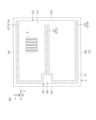
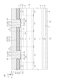
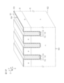
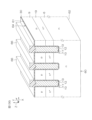
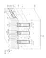
- the semiconductor device 1A includes a plurality of trench gate structures 10 formed on the first main surface 3.
- a gate potential is applied to the trench gate structure 10 .
- a plurality of trench gate structures 10 penetrate base region 9 to drift region 6 .
- the plurality of trench gate structures 10 are arranged in the first direction X at intervals in a plan view, and are each formed in a strip shape extending in the second direction Y. As shown in FIG. That is, the plurality of trench gate structures 10 are arranged in stripes extending in the second direction Y. As shown in FIG.
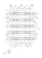
- the plurality of electrode recess portions 15 of one trench gate structure 10 face the plurality of electrode recess portions 15 of the other trench gate structure 10 in the first direction X. ing.
- the plurality of electrode recess portions 15 are formed in a matrix with intervals in the first direction X and the second direction Y. As shown in FIG.
- a plurality of CS regions 19 are formed in regions between the bottom of base region 9 and the bottom wall of trench gate structure 10 with respect to the thickness direction of chip 2 .
- the plurality of CS regions 19 preferably have bottoms located closer to the base region 9 than the bottom wall of the trench gate structure 10 .
- the bottoms of the plurality of CS regions 19 are preferably located closer to the bottom wall of the trench gate structure 10 than the intermediate portion of the trench gate structure 10 .
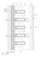
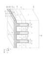
- the in-base region 20 is formed in the region between the bottom of the base region 9 and the bottom of the emitter region 17 within the base region 9 .
- the in-base region 20 has a p-type impurity concentration higher than that of the base region 9 .
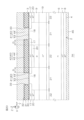
- Interlayer insulating film 31 covers first main surface 3 .
- the interlayer insulating film 31 has a connection hole 33 that partially exposes the emitter region 17 .
- the connection hole 33 is formed spaced apart from the in-base region 20 in the direction along the first main surface 3 .
- the emitter connection electrode 41 is arranged inside the connection hole 33 . Emitter connection electrode 41 is electrically connected to base region 9 and emitter region 17 within connection hole 33 .
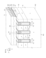
- the etching method may be a wet etching method and/or a dry etching method. Unwanted portions of wafer 60 are removed through base region 9 until drift region 6 is exposed. Thereby, a plurality of gate trenches 11 are formed through the base region 9 to reach the drift region 6 . The first mask 63 is then removed.
- an n-type buffer region 7 is formed in the surface layer portion of the second wafer main surface 62 .
- the buffer region 7 may be formed by introducing an n-type impurity into the entire surface layer portion of the second wafer main surface 62 .
- a p-type collector region 8 is formed in the surface layer portion of the second wafer main surface 62 .
- Collector region 8 may be formed by implanting p-type impurities into the entire surface layer of second wafer main surface 62 .
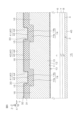
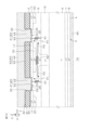
- the plurality of second electrode films 82 are embedded in the plurality of connections with the first electrode film 81 interposed therebetween.
- the plurality of second electrode films 82 cover the wall surfaces of the plurality of recess insulators 14 , the plurality of chip recess portions 23 and the wall surfaces of the plurality of connection holes 33 with the first electrode films 81 interposed in the plurality of connection holes 33 .
- the plurality of second electrode films 82 include at least one of a W (tungsten) film, a Mo (molybdenum) film, a Ni (nickel) film, a pure Al film, a pure Cu film, an Al alloy film and a Cu alloy film. You can stay.
- the plurality of second electrode films 82 preferably include a W film.
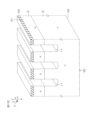
- FIG. 22 is a plan view showing a main part of a semiconductor device 1J according to the tenth embodiment.
- 23 is a cross-sectional view taken along line XXIII-XXIII shown in FIG. 22.
- FIG. 24 is a cross-sectional view taken along line XXIV-XXIV shown in FIG. 22.
- semiconductor device 1J is an RC-IGBT semiconductor device (semiconductor switching device) having an RC-IGBT (Reverse Conducting-IGBT) integrally including an IGBT and a diode.
- the diode is the freewheeling diode for the IGBT.
- the plurality of diode regions 92 are arranged adjacent to at least one IGBT region 91 .
- the plurality of diode regions 92 are arranged alternately with the plurality of IGBT regions 91 along the first direction X in this embodiment.
- a first end and a second end of each RC-IGBT region 90 are formed by an IGBT region 91 or a diode region 92, respectively.
- the trench gate structure (10) includes a trench (11) formed in the main surface (3), a gate insulating film (12) covering the wall surface of the trench (11), the gate insulating film (12) ) sandwiched in the trench (11), an electrode recess portion (15) formed in the electrode surface of the gate buried electrode (13), and the electrode recess portion (15) said insulating film (31) covering said gate buried electrode (13) and forming said contact hole (33) exposing said recess insulator (14) and the connection electrode (41) has a portion facing the gate buried electrode (13) with the recess insulator (14) interposed in the connection hole (33).
- the semiconductor device (1A to 1J) according to any one.
Landscapes
- Electrodes Of Semiconductors (AREA)
Priority Applications (3)
| Application Number | Priority Date | Filing Date | Title |
|---|---|---|---|
| CN202280091818.1A CN118696417A (zh) | 2022-02-18 | 2022-11-29 | 半导体装置 |
| JP2024500964A JPWO2023157422A1 (https=) | 2022-02-18 | 2022-11-29 | |
| US18/806,730 US20240405110A1 (en) | 2022-02-18 | 2024-08-16 | Semiconductor device |
Applications Claiming Priority (2)
| Application Number | Priority Date | Filing Date | Title |
|---|---|---|---|
| JP2022024185 | 2022-02-18 | ||
| JP2022-024185 | 2022-02-18 |
Related Child Applications (1)
| Application Number | Title | Priority Date | Filing Date |
|---|---|---|---|
| US18/806,730 Continuation US20240405110A1 (en) | 2022-02-18 | 2024-08-16 | Semiconductor device |
Publications (1)
| Publication Number | Publication Date |
|---|---|
| WO2023157422A1 true WO2023157422A1 (ja) | 2023-08-24 |
Family
ID=87577978
Family Applications (1)
| Application Number | Title | Priority Date | Filing Date |
|---|---|---|---|
| PCT/JP2022/043909 Ceased WO2023157422A1 (ja) | 2022-02-18 | 2022-11-29 | 半導体装置 |
Country Status (4)
| Country | Link |
|---|---|
| US (1) | US20240405110A1 (https=) |
| JP (1) | JPWO2023157422A1 (https=) |
| CN (1) | CN118696417A (https=) |
| WO (1) | WO2023157422A1 (https=) |
Families Citing this family (2)
| Publication number | Priority date | Publication date | Assignee | Title |
|---|---|---|---|---|
| JP2024098458A (ja) * | 2023-01-10 | 2024-07-23 | 富士電機株式会社 | 半導体装置 |
| JP7839123B2 (ja) * | 2023-03-23 | 2026-04-01 | 株式会社東芝 | 半導体装置 |
Citations (6)
| Publication number | Priority date | Publication date | Assignee | Title |
|---|---|---|---|---|
| JP2001308328A (ja) * | 2000-04-24 | 2001-11-02 | Toyota Central Res & Dev Lab Inc | 絶縁ゲート型半導体装置 |
| JP2002016080A (ja) * | 2000-06-28 | 2002-01-18 | Toshiba Corp | トレンチゲート型mosfetの製造方法 |
| JP2008103375A (ja) * | 2006-10-17 | 2008-05-01 | Fuji Electric Device Technology Co Ltd | 半導体装置およびその製造方法 |
| JP2009065117A (ja) * | 2007-08-10 | 2009-03-26 | Rohm Co Ltd | 半導体装置および半導体装置の製造方法 |
| JP2018156996A (ja) * | 2017-03-15 | 2018-10-04 | 富士電機株式会社 | 半導体装置 |
| WO2019103135A1 (ja) * | 2017-11-24 | 2019-05-31 | ローム株式会社 | 半導体装置 |
-
2022
- 2022-11-29 CN CN202280091818.1A patent/CN118696417A/zh active Pending
- 2022-11-29 JP JP2024500964A patent/JPWO2023157422A1/ja active Pending
- 2022-11-29 WO PCT/JP2022/043909 patent/WO2023157422A1/ja not_active Ceased
-
2024
- 2024-08-16 US US18/806,730 patent/US20240405110A1/en active Pending
Patent Citations (6)
| Publication number | Priority date | Publication date | Assignee | Title |
|---|---|---|---|---|
| JP2001308328A (ja) * | 2000-04-24 | 2001-11-02 | Toyota Central Res & Dev Lab Inc | 絶縁ゲート型半導体装置 |
| JP2002016080A (ja) * | 2000-06-28 | 2002-01-18 | Toshiba Corp | トレンチゲート型mosfetの製造方法 |
| JP2008103375A (ja) * | 2006-10-17 | 2008-05-01 | Fuji Electric Device Technology Co Ltd | 半導体装置およびその製造方法 |
| JP2009065117A (ja) * | 2007-08-10 | 2009-03-26 | Rohm Co Ltd | 半導体装置および半導体装置の製造方法 |
| JP2018156996A (ja) * | 2017-03-15 | 2018-10-04 | 富士電機株式会社 | 半導体装置 |
| WO2019103135A1 (ja) * | 2017-11-24 | 2019-05-31 | ローム株式会社 | 半導体装置 |
Also Published As
| Publication number | Publication date |
|---|---|
| CN118696417A (zh) | 2024-09-24 |
| JPWO2023157422A1 (https=) | 2023-08-24 |
| US20240405110A1 (en) | 2024-12-05 |
Similar Documents
| Publication | Publication Date | Title |
|---|---|---|
| US20230154986A1 (en) | Insulated-gate semiconductor device and method of manufacturing the same | |
| CN113314603B (zh) | 半导体装置 | |
| JP7327672B2 (ja) | 半導体装置 | |
| CN114497200B (zh) | 半导体元件、半导体装置 | |
| CN111697076B (zh) | 半导体装置 | |
| JP7343315B2 (ja) | 炭化ケイ素半導体装置 | |
| US11664448B2 (en) | Semiconductor device | |
| US11177360B2 (en) | Semiconductor device | |
| US20240405110A1 (en) | Semiconductor device | |
| JP2020167230A (ja) | 半導体装置 | |
| JP2020177957A (ja) | 半導体装置 | |
| WO2023157395A1 (ja) | 半導体装置およびその製造方法 | |
| US20240088221A1 (en) | Semiconductor device | |
| JP3329973B2 (ja) | 半導体装置およびその製造方法 | |
| JP7726821B6 (ja) | 半導体装置及び製造方法 | |
| JP5023423B2 (ja) | 縦型絶縁ゲート型電界効果トランジスタおよびその製造方法 | |
| CN120226466A (zh) | 半导体装置 | |
| US6078065A (en) | Bilaterally controllable thyristor | |
| CN114823884A (zh) | 半导体装置 | |
| CN116018689A (zh) | 半导体装置 | |
| US20250393287A1 (en) | Semiconductor device | |
| US20250040207A1 (en) | Semiconductor device | |
| US20260076186A1 (en) | Power semiconductor devices | |
| US20240371993A1 (en) | Semiconductor device and method of manufacturing semiconductor device | |
| US20250261439A1 (en) | Vertical semiconductor device |
Legal Events
| Date | Code | Title | Description |
|---|---|---|---|
| 121 | Ep: the epo has been informed by wipo that ep was designated in this application |
Ref document number: 22927311 Country of ref document: EP Kind code of ref document: A1 |
|
| ENP | Entry into the national phase |
Ref document number: 2024500964 Country of ref document: JP Kind code of ref document: A |
|
| WWE | Wipo information: entry into national phase |
Ref document number: 202280091818.1 Country of ref document: CN |
|
| NENP | Non-entry into the national phase |
Ref country code: DE |
|
| 122 | Ep: pct application non-entry in european phase |
Ref document number: 22927311 Country of ref document: EP Kind code of ref document: A1 |