WO2023157422A1 - Semiconductor device - Google Patents
Semiconductor device Download PDFInfo
- Publication number
- WO2023157422A1 WO2023157422A1 PCT/JP2022/043909 JP2022043909W WO2023157422A1 WO 2023157422 A1 WO2023157422 A1 WO 2023157422A1 JP 2022043909 W JP2022043909 W JP 2022043909W WO 2023157422 A1 WO2023157422 A1 WO 2023157422A1
- Authority
- WO
- WIPO (PCT)
- Prior art keywords
- region
- electrode
- semiconductor device
- base region
- main surface
- Prior art date
Links
- 239000004065 semiconductor Substances 0.000 title claims abstract description 170
- 239000012535 impurity Substances 0.000 claims abstract description 35
- 239000002344 surface layer Substances 0.000 claims abstract description 27
- 239000012212 insulator Substances 0.000 claims description 76
- 239000011229 interlayer Substances 0.000 description 47
- 238000000034 method Methods 0.000 description 30
- 238000005530 etching Methods 0.000 description 15
- 230000003071 parasitic effect Effects 0.000 description 12
- VYPSYNLAJGMNEJ-UHFFFAOYSA-N Silicium dioxide Chemical compound O=[Si]=O VYPSYNLAJGMNEJ-UHFFFAOYSA-N 0.000 description 11
- 229910052814 silicon oxide Inorganic materials 0.000 description 11
- 229910045601 alloy Inorganic materials 0.000 description 10
- 239000000956 alloy Substances 0.000 description 10
- 229910052751 metal Inorganic materials 0.000 description 10
- 239000002184 metal Substances 0.000 description 10
- 230000000694 effects Effects 0.000 description 9
- XUIMIQQOPSSXEZ-UHFFFAOYSA-N Silicon Chemical compound [Si] XUIMIQQOPSSXEZ-UHFFFAOYSA-N 0.000 description 7
- PXHVJJICTQNCMI-UHFFFAOYSA-N nickel Substances [Ni] PXHVJJICTQNCMI-UHFFFAOYSA-N 0.000 description 7
- 229910052710 silicon Inorganic materials 0.000 description 7
- 239000010703 silicon Substances 0.000 description 7
- 238000001312 dry etching Methods 0.000 description 6
- 239000002356 single layer Substances 0.000 description 6
- 239000000758 substrate Substances 0.000 description 6
- 238000001039 wet etching Methods 0.000 description 6
- 229910000881 Cu alloy Inorganic materials 0.000 description 5
- 229910052581 Si3N4 Inorganic materials 0.000 description 5
- 210000000746 body region Anatomy 0.000 description 5
- TWNQGVIAIRXVLR-UHFFFAOYSA-N oxo(oxoalumanyloxy)alumane Chemical compound O=[Al]O[Al]=O TWNQGVIAIRXVLR-UHFFFAOYSA-N 0.000 description 5
- HQVNEWCFYHHQES-UHFFFAOYSA-N silicon nitride Chemical compound N12[Si]34N5[Si]62N3[Si]51N64 HQVNEWCFYHHQES-UHFFFAOYSA-N 0.000 description 5
- 229910016570 AlCu Inorganic materials 0.000 description 4
- ATJFFYVFTNAWJD-UHFFFAOYSA-N Tin Chemical compound [Sn] ATJFFYVFTNAWJD-UHFFFAOYSA-N 0.000 description 4
- 239000000969 carrier Substances 0.000 description 4
- 239000011159 matrix material Substances 0.000 description 4
- 238000005192 partition Methods 0.000 description 4
- 238000009825 accumulation Methods 0.000 description 3
- 238000005229 chemical vapour deposition Methods 0.000 description 3
- 239000013078 crystal Substances 0.000 description 3
- 238000009413 insulation Methods 0.000 description 3
- 239000010410 layer Substances 0.000 description 3
- 229910021420 polycrystalline silicon Inorganic materials 0.000 description 3
- 229920005591 polysilicon Polymers 0.000 description 3
- 239000005368 silicate glass Substances 0.000 description 3
- 229910000789 Aluminium-silicon alloy Inorganic materials 0.000 description 2
- 239000011810 insulating material Substances 0.000 description 2
- 238000004519 manufacturing process Methods 0.000 description 2
- 239000012528 membrane Substances 0.000 description 2
- 230000003647 oxidation Effects 0.000 description 2
- 238000007254 oxidation reaction Methods 0.000 description 2
- 238000005498 polishing Methods 0.000 description 2
- HBMJWWWQQXIZIP-UHFFFAOYSA-N silicon carbide Chemical compound [Si+]#[C-] HBMJWWWQQXIZIP-UHFFFAOYSA-N 0.000 description 2
- 229910010271 silicon carbide Inorganic materials 0.000 description 2
- 238000004544 sputter deposition Methods 0.000 description 2
- 238000007740 vapor deposition Methods 0.000 description 2
- 229910000838 Al alloy Inorganic materials 0.000 description 1
- ZOKXTWBITQBERF-UHFFFAOYSA-N Molybdenum Chemical compound [Mo] ZOKXTWBITQBERF-UHFFFAOYSA-N 0.000 description 1
- OAICVXFJPJFONN-UHFFFAOYSA-N Phosphorus Chemical compound [P] OAICVXFJPJFONN-UHFFFAOYSA-N 0.000 description 1
- GDFCWFBWQUEQIJ-UHFFFAOYSA-N [B].[P] Chemical compound [B].[P] GDFCWFBWQUEQIJ-UHFFFAOYSA-N 0.000 description 1
- 230000001154 acute effect Effects 0.000 description 1
- 230000015572 biosynthetic process Effects 0.000 description 1
- 239000004020 conductor Substances 0.000 description 1
- 230000007423 decrease Effects 0.000 description 1
- 230000003247 decreasing effect Effects 0.000 description 1
- 230000006866 deterioration Effects 0.000 description 1
- 238000010586 diagram Methods 0.000 description 1
- 239000007943 implant Substances 0.000 description 1
- 229910052750 molybdenum Inorganic materials 0.000 description 1
- 239000011733 molybdenum Substances 0.000 description 1
- 229910052759 nickel Inorganic materials 0.000 description 1
- 230000002093 peripheral effect Effects 0.000 description 1
- 238000003860 storage Methods 0.000 description 1
- WFKWXMTUELFFGS-UHFFFAOYSA-N tungsten Chemical compound [W] WFKWXMTUELFFGS-UHFFFAOYSA-N 0.000 description 1
- 229910052721 tungsten Inorganic materials 0.000 description 1
- 239000010937 tungsten Substances 0.000 description 1
Images


Classifications
-
- H—ELECTRICITY
- H01—ELECTRIC ELEMENTS
- H01L—SEMICONDUCTOR DEVICES NOT COVERED BY CLASS H10
- H01L29/00—Semiconductor devices adapted for rectifying, amplifying, oscillating or switching, or capacitors or resistors with at least one potential-jump barrier or surface barrier, e.g. PN junction depletion layer or carrier concentration layer; Details of semiconductor bodies or of electrodes thereof ; Multistep manufacturing processes therefor
- H01L29/66—Types of semiconductor device ; Multistep manufacturing processes therefor
- H01L29/66007—Multistep manufacturing processes
- H01L29/66075—Multistep manufacturing processes of devices having semiconductor bodies comprising group 14 or group 13/15 materials
- H01L29/66083—Multistep manufacturing processes of devices having semiconductor bodies comprising group 14 or group 13/15 materials the devices being controllable only by variation of the electric current supplied or the electric potential applied, to one or more of the electrodes carrying the current to be rectified, amplified, oscillated or switched, e.g. two-terminal devices
-
- H—ELECTRICITY
- H01—ELECTRIC ELEMENTS
- H01L—SEMICONDUCTOR DEVICES NOT COVERED BY CLASS H10
- H01L29/00—Semiconductor devices adapted for rectifying, amplifying, oscillating or switching, or capacitors or resistors with at least one potential-jump barrier or surface barrier, e.g. PN junction depletion layer or carrier concentration layer; Details of semiconductor bodies or of electrodes thereof ; Multistep manufacturing processes therefor
- H01L29/66—Types of semiconductor device ; Multistep manufacturing processes therefor
- H01L29/66007—Multistep manufacturing processes
- H01L29/66075—Multistep manufacturing processes of devices having semiconductor bodies comprising group 14 or group 13/15 materials
- H01L29/66227—Multistep manufacturing processes of devices having semiconductor bodies comprising group 14 or group 13/15 materials the devices being controllable only by the electric current supplied or the electric potential applied, to an electrode which does not carry the current to be rectified, amplified or switched, e.g. three-terminal devices
- H01L29/66409—Unipolar field-effect transistors
- H01L29/66477—Unipolar field-effect transistors with an insulated gate, i.e. MISFET
-
- H—ELECTRICITY
- H01—ELECTRIC ELEMENTS
- H01L—SEMICONDUCTOR DEVICES NOT COVERED BY CLASS H10
- H01L29/00—Semiconductor devices adapted for rectifying, amplifying, oscillating or switching, or capacitors or resistors with at least one potential-jump barrier or surface barrier, e.g. PN junction depletion layer or carrier concentration layer; Details of semiconductor bodies or of electrodes thereof ; Multistep manufacturing processes therefor
- H01L29/66—Types of semiconductor device ; Multistep manufacturing processes therefor
- H01L29/68—Types of semiconductor device ; Multistep manufacturing processes therefor controllable by only the electric current supplied, or only the electric potential applied, to an electrode which does not carry the current to be rectified, amplified or switched
- H01L29/70—Bipolar devices
- H01L29/72—Transistor-type devices, i.e. able to continuously respond to applied control signals
- H01L29/739—Transistor-type devices, i.e. able to continuously respond to applied control signals controlled by field-effect, e.g. bipolar static induction transistors [BSIT]
-
- H—ELECTRICITY
- H01—ELECTRIC ELEMENTS
- H01L—SEMICONDUCTOR DEVICES NOT COVERED BY CLASS H10
- H01L29/00—Semiconductor devices adapted for rectifying, amplifying, oscillating or switching, or capacitors or resistors with at least one potential-jump barrier or surface barrier, e.g. PN junction depletion layer or carrier concentration layer; Details of semiconductor bodies or of electrodes thereof ; Multistep manufacturing processes therefor
- H01L29/66—Types of semiconductor device ; Multistep manufacturing processes therefor
- H01L29/68—Types of semiconductor device ; Multistep manufacturing processes therefor controllable by only the electric current supplied, or only the electric potential applied, to an electrode which does not carry the current to be rectified, amplified or switched
- H01L29/76—Unipolar devices, e.g. field effect transistors
- H01L29/772—Field effect transistors
- H01L29/78—Field effect transistors with field effect produced by an insulated gate
-
- H—ELECTRICITY
- H01—ELECTRIC ELEMENTS
- H01L—SEMICONDUCTOR DEVICES NOT COVERED BY CLASS H10
- H01L29/00—Semiconductor devices adapted for rectifying, amplifying, oscillating or switching, or capacitors or resistors with at least one potential-jump barrier or surface barrier, e.g. PN junction depletion layer or carrier concentration layer; Details of semiconductor bodies or of electrodes thereof ; Multistep manufacturing processes therefor
- H01L29/66—Types of semiconductor device ; Multistep manufacturing processes therefor
- H01L29/86—Types of semiconductor device ; Multistep manufacturing processes therefor controllable only by variation of the electric current supplied, or only the electric potential applied, to one or more of the electrodes carrying the current to be rectified, amplified, oscillated or switched
- H01L29/861—Diodes
- H01L29/868—PIN diodes
Definitions
- FIG. 10 is a cross-sectional perspective view with the interlayer insulating film removed from FIG.
- FIG. 11 is a cross-sectional view showing a semiconductor device according to a reference example together with resistor symbols.
- FIG. 12 is a cross-sectional view showing the semiconductor device according to the embodiment together with resistor symbols.
- 13A is a cross-sectional perspective view showing an example of a method for manufacturing the semiconductor device shown in FIG. 1.
- FIG. 13B is a cross-sectional perspective view showing a step after FIG. 13A.
- FIG. 13C is a cross-sectional perspective view showing a step after FIG. 13B.
- FIG. 13D is a cross-sectional perspective view showing a step after FIG. 13C.
- FIG. 13A is a cross-sectional perspective view showing an example of a method for manufacturing the semiconductor device shown in FIG. 1.
- FIG. 13B is a cross-sectional perspective view showing a step after FIG. 13A.
- FIG. 13C is a cross-
- FIG. 13M is a cross-sectional perspective view showing a step after FIG. 13L.
- FIG. 13N is a cross-sectional perspective view showing a step after FIG. 13M.
- FIG. 13O is a cross-sectional perspective view showing a step after FIG. 13N.
- FIG. 13P is a cross-sectional perspective view showing a step after FIG. 13O.
- FIG. 13Q is a cross-sectional perspective view showing a step after FIG. 13P.
- FIG. 13R is a cross-sectional perspective view showing a step after FIG. 13Q.
- FIG. 14 is a cross-sectional view showing the semiconductor device according to the second embodiment.
- FIG. 15 is a cross-sectional view showing the semiconductor device according to the third embodiment.
- the semiconductor device 1A includes a plurality of trench gate structures 10 formed on the first main surface 3.
- a gate potential is applied to the trench gate structure 10 .
- a plurality of trench gate structures 10 penetrate base region 9 to drift region 6 .
- the plurality of trench gate structures 10 are arranged in the first direction X at intervals in a plan view, and are each formed in a strip shape extending in the second direction Y. As shown in FIG. That is, the plurality of trench gate structures 10 are arranged in stripes extending in the second direction Y. As shown in FIG.
- the plurality of electrode recess portions 15 of one trench gate structure 10 face the plurality of electrode recess portions 15 of the other trench gate structure 10 in the first direction X. ing.
- the plurality of electrode recess portions 15 are formed in a matrix with intervals in the first direction X and the second direction Y. As shown in FIG.
- a plurality of CS regions 19 are formed in regions between the bottom of base region 9 and the bottom wall of trench gate structure 10 with respect to the thickness direction of chip 2 .
- the plurality of CS regions 19 preferably have bottoms located closer to the base region 9 than the bottom wall of the trench gate structure 10 .
- the bottoms of the plurality of CS regions 19 are preferably located closer to the bottom wall of the trench gate structure 10 than the intermediate portion of the trench gate structure 10 .
- the in-base region 20 is formed in the region between the bottom of the base region 9 and the bottom of the emitter region 17 within the base region 9 .
- the in-base region 20 has a p-type impurity concentration higher than that of the base region 9 .
- Interlayer insulating film 31 covers first main surface 3 .
- the interlayer insulating film 31 has a connection hole 33 that partially exposes the emitter region 17 .
- the connection hole 33 is formed spaced apart from the in-base region 20 in the direction along the first main surface 3 .
- the emitter connection electrode 41 is arranged inside the connection hole 33 . Emitter connection electrode 41 is electrically connected to base region 9 and emitter region 17 within connection hole 33 .
- the etching method may be a wet etching method and/or a dry etching method. Unwanted portions of wafer 60 are removed through base region 9 until drift region 6 is exposed. Thereby, a plurality of gate trenches 11 are formed through the base region 9 to reach the drift region 6 . The first mask 63 is then removed.
- an n-type buffer region 7 is formed in the surface layer portion of the second wafer main surface 62 .
- the buffer region 7 may be formed by introducing an n-type impurity into the entire surface layer portion of the second wafer main surface 62 .
- a p-type collector region 8 is formed in the surface layer portion of the second wafer main surface 62 .
- Collector region 8 may be formed by implanting p-type impurities into the entire surface layer of second wafer main surface 62 .
- the plurality of second electrode films 82 are embedded in the plurality of connections with the first electrode film 81 interposed therebetween.
- the plurality of second electrode films 82 cover the wall surfaces of the plurality of recess insulators 14 , the plurality of chip recess portions 23 and the wall surfaces of the plurality of connection holes 33 with the first electrode films 81 interposed in the plurality of connection holes 33 .
- the plurality of second electrode films 82 include at least one of a W (tungsten) film, a Mo (molybdenum) film, a Ni (nickel) film, a pure Al film, a pure Cu film, an Al alloy film and a Cu alloy film. You can stay.
- the plurality of second electrode films 82 preferably include a W film.
- FIG. 22 is a plan view showing a main part of a semiconductor device 1J according to the tenth embodiment.
- 23 is a cross-sectional view taken along line XXIII-XXIII shown in FIG. 22.
- FIG. 24 is a cross-sectional view taken along line XXIV-XXIV shown in FIG. 22.
- semiconductor device 1J is an RC-IGBT semiconductor device (semiconductor switching device) having an RC-IGBT (Reverse Conducting-IGBT) integrally including an IGBT and a diode.
- the diode is the freewheeling diode for the IGBT.
- the plurality of diode regions 92 are arranged adjacent to at least one IGBT region 91 .
- the plurality of diode regions 92 are arranged alternately with the plurality of IGBT regions 91 along the first direction X in this embodiment.
- a first end and a second end of each RC-IGBT region 90 are formed by an IGBT region 91 or a diode region 92, respectively.
- the trench gate structure (10) includes a trench (11) formed in the main surface (3), a gate insulating film (12) covering the wall surface of the trench (11), the gate insulating film (12) ) sandwiched in the trench (11), an electrode recess portion (15) formed in the electrode surface of the gate buried electrode (13), and the electrode recess portion (15) said insulating film (31) covering said gate buried electrode (13) and forming said contact hole (33) exposing said recess insulator (14) and the connection electrode (41) has a portion facing the gate buried electrode (13) with the recess insulator (14) interposed in the connection hole (33).
- the semiconductor device (1A to 1J) according to any one.
Abstract
This semiconductor device comprises: a chip having a main surface; a first conductivity-type base region formed on the surface layer part of the main surface; a trench gate structure formed on the main surface so as to penetrate through the base region; a second conductivity-type emitter region formed in a region along the trench gate structure in the surface layer part of the base region; a first conductivity-type in-base region formed in a region between the bottom part of the base region and the bottom part of the emitter region in the base region, and having an impurity concentration higher than that of the base region; an insulating film which covers the main surface and has a connecting hole for exposing a part of the emitter region at a distance from the in-base region in a direction along the main surface; and a connecting electrode which is disposed in the connecting hole so as to be electrically connected to the base region and the emitter region.
Description
この出願は、2022年2月18日提出の日本国特許出願2022-024185号に基づく優先権を主張しており、この出願の全内容はここに引用により組み込まれる。本開示は、半導体装置に関する。
This application claims priority based on Japanese Patent Application No. 2022-024185 filed on February 18, 2022, and the entire contents of this application are incorporated herein by reference. The present disclosure relates to semiconductor devices.
特許文献1は、半導体基板、p型のボディ領域、トレンチゲート構造、n型のエミッタ領域、絶縁膜、p型のコンタクト領域およびエミッタ電極を含む半導体装置を開示している。半導体基板は、主面を有している。ボディ領域は、主面の表層部に形成されている。トレンチゲート構造は、ボディ領域を貫通するように主面に形成されている。エミッタ領域は、トレンチゲート構造に接するようにボディ領域内に形成されている。
Patent Document 1 discloses a semiconductor device including a semiconductor substrate, a p-type body region, a trench gate structure, an n-type emitter region, an insulating film, a p-type contact region and an emitter electrode. The semiconductor substrate has a main surface. The body region is formed in the surface layer portion of the main surface. A trench gate structure is formed on the main surface to penetrate the body region. An emitter region is formed in the body region to contact the trench gate structure.
絶縁膜は、主面を被覆し、エミッタ領域を露出させるコンタクト溝を有している。コンタクト領域は、コンタクト溝から露出するようにボディ領域内に形成されている。エミッタ電極は、コンタクト溝内でエミッタ領域およびコンタクト領域に電気的に接続されている。
The insulating film covers the main surface and has a contact groove that exposes the emitter region. A contact region is formed in the body region so as to be exposed from the contact trench. An emitter electrode is electrically connected to the emitter region and the contact region within the contact trench.
一実施形態は、電気的特性を向上できる半導体装置を提供する。
One embodiment provides a semiconductor device capable of improving electrical characteristics.
一実施形態は、主面を有するチップと、前記主面の表層部に形成された第1導電型のベース領域と、前記ベース領域を貫通するように前記主面に形成されたトレンチゲート構造と、前記ベース領域の表層部において前記トレンチゲート構造に沿う領域に形成された第2導電型のエミッタ領域と、前記ベース領域内において前記ベース領域の底部および前記エミッタ領域の底部の間の領域に形成され、前記ベース領域よりも高い不純物濃度を有する第1導電型のインベース領域と、前記主面を被覆し、前記主面に沿う方向に前記インベース領域から間隔を空けて前記エミッタ領域の一部を露出させる接続孔を有する絶縁膜と、前記ベース領域および前記エミッタ領域に電気的に接続されるように前記接続孔内に配置された接続電極と、を含む、半導体装置を提供する。
One embodiment comprises a chip having a main surface, a base region of a first conductivity type formed in a surface layer portion of the main surface, and a trench gate structure formed in the main surface so as to penetrate the base region. an emitter region of the second conductivity type formed in a region along the trench gate structure in the surface layer portion of the base region; an inbase region of a first conductivity type having an impurity concentration higher than that of the base region; and an emitter region covering the main surface and spaced from the inbase region in a direction along the main surface. and a connection electrode disposed in the contact hole so as to be electrically connected to the base region and the emitter region.
上述のまたはさらに他の目的、特徴および効果は、添付図面の参照によって説明される実施形態により明らかにされる。
The above or further objects, features and advantages will be made clear by the embodiments described with reference to the accompanying drawings.
以下、添付図面を参照して、実施形態が詳細に説明される。添付図面は、模式図であり、厳密に図示されたものではなく、縮尺等は必ずしも一致しない。また、添付図面の間で対応する構造には同一の参照符号が付され、重複する説明は省略または簡略化される。説明が省略または簡略化された構造については、省略または簡略化される前になされた説明が適用される。
Hereinafter, embodiments will be described in detail with reference to the accompanying drawings. The attached drawings are schematic diagrams and are not strictly illustrated, and the scales and the like do not necessarily match. In addition, the same reference numerals are given to structures corresponding to each other in the accompanying drawings, and duplicate descriptions are omitted or simplified. For structures whose descriptions are omitted or simplified, the descriptions given before the omissions or simplifications apply.
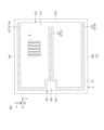
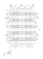
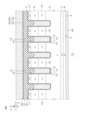
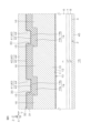
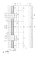
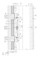
図1は、第1実施形態に係る半導体装置1Aを示す平面図である。図2は、図1に示す領域IIの拡大図である。図3は、図2に示すIII-III線に沿う断面図である。図4は、図2に示すIV-IV線に沿う断面図である。図5は、図2に示すV-V線に沿う断面図である。図6は、図2に示すVI-VI線に沿う断面図である。図7は、図2に示すVII-VII線に沿う断面図である。図8は、図1に示す半導体装置1Aの要部を示す断面斜視図である。図9は、図8からエミッタ電極40が取り除かれた断面斜視図である。図10は、図9から層間絶縁膜31が取り除かれた断面斜視図である。
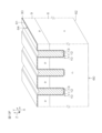
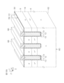
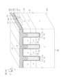
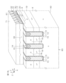
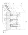
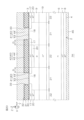
FIG. 1 is a plan view showing a semiconductor device 1A according to the first embodiment. FIG. 2 is an enlarged view of area II shown in FIG. FIG. 3 is a cross-sectional view taken along line III-III shown in FIG. FIG. 4 is a cross-sectional view taken along line IV-IV shown in FIG. FIG. 5 is a cross-sectional view taken along line V-V shown in FIG. FIG. 6 is a cross-sectional view taken along line VI-VI shown in FIG. FIG. 7 is a cross-sectional view taken along line VII-VII shown in FIG. FIG. 8 is a cross-sectional perspective view showing a main part of the semiconductor device 1A shown in FIG. FIG. 9 is a cross-sectional perspective view with the emitter electrode 40 removed from FIG. FIG. 10 is a cross-sectional perspective view with the interlayer insulating film 31 removed from FIG.
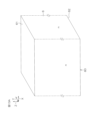
図1~図10を参照して、半導体装置1Aは、IGBT(Insulated Gate Bipolar Transistor)を含む半導体スイッチング装置である。半導体装置1Aは、六面体形状(具体的には直方体形状)のチップ2を含む。チップ2は、この形態(this embodiment)では、シリコン単結晶基板(半導体基板)からなる単層構造を有している。チップ2は、50μm以上400μm以下の厚さを有していてもよい。
1 to 10, semiconductor device 1A is a semiconductor switching device including an IGBT (Insulated Gate Bipolar Transistor). A semiconductor device 1A includes a hexahedral (specifically rectangular parallelepiped) chip 2 . The chip 2, in this embodiment, has a single-layer structure made of a silicon single crystal substrate (semiconductor substrate). The chip 2 may have a thickness of 50 μm or more and 400 μm or less.
チップ2は、一方側の第1主面3、他方側の第2主面4、ならびに、第1主面3および第2主面4を接続する第1~第4側面5A~5Dを有している。第1主面3および第2主面4は、それらの法線方向Zから見た平面視(以下、単に「平面視」という。)において四角形状に形成されている。法線方向Zは、チップ2の厚さ方向でもある。
The chip 2 has a first main surface 3 on one side, a second main surface 4 on the other side, and first to fourth side surfaces 5A to 5D connecting the first main surface 3 and the second main surface 4. ing. The first main surface 3 and the second main surface 4 are formed in a quadrangular shape in plan view (hereinafter simply referred to as "plan view") as seen from the normal direction Z thereof. The normal direction Z is also the thickness direction of the chip 2 .
第1側面5Aおよび第2側面5Bは、第1主面3に沿う第1方向Xに延び、第1方向Xに交差(具体的には直交)する第2方向Yに対向している。第3側面5Cおよび第4側面5Dは、第2方向Yに延び、第1方向Xに対向している。
The first side surface 5A and the second side surface 5B extend in the first direction X along the first main surface 3 and face the second direction Y intersecting (specifically, perpendicular to) the first direction X. The third side surface 5C and the fourth side surface 5D extend in the second direction Y and face the first direction X. As shown in FIG.
半導体装置1Aは、チップ2の内部に形成されたn型のドリフト領域6を含む。ドリフト領域6は、チップ2の内部の全域に形成されている。この形態では、チップ2がn型の半導体チップからなり、ドリフト領域6はチップ2を利用して形成されている。
The semiconductor device 1A includes an n-type drift region 6 formed inside the chip 2 . Drift region 6 is formed in the entire interior of chip 2 . In this form, the chip 2 is an n-type semiconductor chip, and the drift region 6 is formed using the chip 2 .
半導体装置1Aは、第2主面4の表層部に形成されたn型のバッファ領域7を含む。バッファ領域7は、第2主面4に沿って層状に延び、第1~第4側面5A~5Dの一部から露出している。バッファ領域7は、ドリフト領域6よりも高いn型不純物濃度を有している。
The semiconductor device 1A includes an n-type buffer region 7 formed in the surface layer portion of the second main surface 4 . The buffer region 7 extends in layers along the second main surface 4 and is partially exposed from the first to fourth side surfaces 5A to 5D. Buffer region 7 has a higher n-type impurity concentration than drift region 6 .
半導体装置1Aは、第2主面4の表層部に形成されたp型のコレクタ領域8を含む。コレクタ領域8は、この形態では、バッファ領域7の第2主面4側の表層部に形成されている。コレクタ領域8は、この形態では、第2主面4の全域において第2主面4に沿って延びる層状に形成されている。コレクタ領域8は、第2主面4および第1~第4側面5A~5Dの一部から露出している。
The semiconductor device 1A includes a p-type collector region 8 formed in the surface layer portion of the second main surface 4 . The collector region 8 is formed in the surface layer portion of the buffer region 7 on the second main surface 4 side in this embodiment. The collector region 8 is formed in a layer shape extending along the second main surface 4 over the entire area of the second main surface 4 in this embodiment. Collector region 8 is exposed from second main surface 4 and part of first to fourth side surfaces 5A to 5D.
半導体装置1Aは、第1主面3の表層部に形成されたp型のベース領域9を含む。ベース領域9は、第1主面3に沿って延びる層状に形成されている。ベース領域9は、チップ2の周縁から間隔を空けてチップ2の内方部に形成されている。
The semiconductor device 1A includes a p-type base region 9 formed in the surface layer portion of the first main surface 3 . Base region 9 is formed in a layered shape extending along first main surface 3 . The base region 9 is formed in the inner portion of the chip 2 with a space from the periphery of the chip 2 .
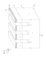
半導体装置1Aは、第1主面3に形成された複数のトレンチゲート構造10を含む。トレンチゲート構造10には、ゲート電位が付与される。複数のトレンチゲート構造10は、ドリフト領域6に至るようにベース領域9を貫通している。複数のトレンチゲート構造10は、平面視において第1方向Xに間隔を空けて配列され、第2方向Yに延びる帯状にそれぞれ形成されている。つまり、複数のトレンチゲート構造10は、第2方向Yに延びるストライプ状に配列されている。
The semiconductor device 1A includes a plurality of trench gate structures 10 formed on the first main surface 3. A gate potential is applied to the trench gate structure 10 . A plurality of trench gate structures 10 penetrate base region 9 to drift region 6 . The plurality of trench gate structures 10 are arranged in the first direction X at intervals in a plan view, and are each formed in a strip shape extending in the second direction Y. As shown in FIG. That is, the plurality of trench gate structures 10 are arranged in stripes extending in the second direction Y. As shown in FIG.
複数のトレンチゲート構造10は、0.5μm以上3μm以下の幅をそれぞれ有していてもよい。複数のトレンチゲート構造10は、1μm以上10μm以下の深さをそれぞれ有していてもよい。複数のトレンチゲート構造10の間の距離(トレンチピッチ)は、0.1μm以上3.5μm以下であってもよい。複数のトレンチゲート構造10の間の距離は、1μm以下であることが好ましい。
The plurality of trench gate structures 10 may each have a width of 0.5 μm or more and 3 μm or less. The plurality of trench gate structures 10 may each have a depth of 1 μm or more and 10 μm or less. A distance (trench pitch) between the plurality of trench gate structures 10 may be 0.1 μm or more and 3.5 μm or less. The distance between trench gate structures 10 is preferably 1 μm or less.
以下、1つのトレンチゲート構造10の構成が説明される。トレンチゲート構造10は、ゲートトレンチ11、ゲート絶縁膜12、ゲート埋設電極13、および、少なくとも1つ(この形態では複数)のリセス絶縁体14を含む。ゲートトレンチ11は、第1主面3から第2主面4に向かって掘り下がり、トレンチゲート構造10の壁面を区画している。
The configuration of one trench gate structure 10 will be described below. Trench gate structure 10 includes gate trench 11 , gate insulating film 12 , gate buried electrode 13 , and at least one (in this embodiment, multiple) recess insulators 14 . The gate trench 11 is dug down from the first main surface 3 toward the second main surface 4 to partition the wall surface of the trench gate structure 10 .
ゲートトレンチ11は、第1主面3に対して垂直な方向に延びている。ゲートトレンチ11は、開口から底壁に向けて開口幅が狭まる先細り形状に形成されていてもよい。ゲートトレンチ11の底壁は、第2主面4に向かう湾曲状に形成されていることが好ましい。むろん、ゲートトレンチ11の底壁は、第1主面3に対して平行に形成されていてもよい。この場合、ゲートトレンチ11の底壁角部は、湾曲状に形成されていることが好ましい。
The gate trench 11 extends in a direction perpendicular to the first principal surface 3 . Gate trench 11 may be formed in a tapered shape in which the opening width narrows from the opening toward the bottom wall. The bottom wall of gate trench 11 is preferably curved toward second main surface 4 . Of course, the bottom wall of gate trench 11 may be formed parallel to first main surface 3 . In this case, the corners of the bottom wall of gate trench 11 are preferably formed in a curved shape.
ゲート絶縁膜12は、ゲートトレンチ11の壁面を膜状に被覆し、ゲートトレンチ11内においてリセス空間を区画している。ゲート絶縁膜12は、酸化シリコン膜、窒化シリコン膜、酸窒化シリコン膜および酸化アルミニウム膜のうちの少なくとも1つを含んでいてもよい。ゲート絶縁膜12は、チップ2の酸化物からなる酸化シリコン膜を含むことが好ましい。
The gate insulating film 12 covers the wall surface of the gate trench 11 in a film form and partitions the recess space within the gate trench 11 . Gate insulating film 12 may include at least one of a silicon oxide film, a silicon nitride film, a silicon oxynitride film and an aluminum oxide film. Gate insulating film 12 preferably includes a silicon oxide film made of the oxide of chip 2 .
ゲート埋設電極13は、ゲート絶縁膜12を挟んでゲートトレンチ11に埋設されている。ゲート埋設電極13には、ゲート電位が付与される。ゲート埋設電極13は、導電性ポリシリコンを含んでいてもよい。ゲート埋設電極13は、ゲート絶縁膜12を挟んでドリフト領域6およびベース領域9に対向している。ゲート埋設電極13は、第1主面3に対してゲートトレンチ11の底壁側に位置する上端部を有していてもよい。
The gate buried electrode 13 is buried in the gate trench 11 with the gate insulating film 12 interposed therebetween. A gate potential is applied to the gate buried electrode 13 . The gate buried electrode 13 may contain conductive polysilicon. The gate buried electrode 13 faces the drift region 6 and the base region 9 with the gate insulating film 12 interposed therebetween. Gate-buried electrode 13 may have an upper end located on the bottom wall side of gate trench 11 with respect to first main surface 3 .
ゲート埋設電極13は、電極面(上端部)においてゲートトレンチ11の延在方向(つまり、第2方向Y)に沿ってゲートトレンチ11の開口側および底壁側に向けて隆起した凹凸構造(uneven structure)を有している。具体的には、ゲート埋設電極13は、上端部において少なくとも1つ(この形態では複数)の電極リセス部15、および、少なくとも1つ(この形態では複数)の電極突出部16を有している。
The gate-buried electrode 13 has an uneven structure (uneven structure) protruding toward the opening side and the bottom wall side of the gate trench 11 along the extension direction (that is, the second direction Y) of the gate trench 11 on the electrode surface (upper end). structure). Specifically, the gate buried electrode 13 has at least one (in this embodiment, a plurality of) electrode recess portions 15 and at least one (in this embodiment, a plurality of) electrode protrusions 16 at its upper end. .
複数の電極リセス部15は、ゲートトレンチ11の電極面からゲートトレンチ11の底壁に向けて窪み、トレンチゲート構造10の延在方向に間隔を空けて形成されている。複数の電極リセス部15は、この形態では、平面視においてトレンチゲート構造10の延在方向に延びる帯状にそれぞれ形成されている。
A plurality of electrode recess portions 15 are recessed from the electrode surface of the gate trench 11 toward the bottom wall of the gate trench 11 and are formed at intervals in the extending direction of the trench gate structure 10 . In this embodiment, the plurality of electrode recess portions 15 are each formed in a strip shape extending in the extending direction of the trench gate structure 10 in plan view.
つまり、各電極リセス部15は、平面視において第2方向Yの長さが第1方向Xの長さよりも大きいレイアウトを有している。各電極リセス部15の長さは、0.5μm以上10μm以下であってもよい。各電極突出部16の長さは、7μm以下であることが好ましい。各電極突出部16の長さは、5μm以下であることが特に好ましい。
That is, each electrode recess portion 15 has a layout in which the length in the second direction Y is longer than the length in the first direction X in plan view. Each electrode recess portion 15 may have a length of 0.5 μm or more and 10 μm or less. The length of each electrode protrusion 16 is preferably 7 μm or less. It is particularly preferable that the length of each electrode protrusion 16 is 5 μm or less.
複数の電極リセス部15は、ゲートトレンチ11の深さ範囲の中間部よりも第1主面3側に位置する底部をそれぞれ有している。具体的には、複数の電極リセス部15の底部は、ベース領域9の底部よりも第1主面3側に位置にしている。つまり、複数の電極リセス部15は、第1主面3の面方向(第1方向X)にベース領域9に対向している。各電極リセス部15の底部は、ゲートトレンチ11の底壁側に向かう窪みを有していてもよい。
The plurality of electrode recess portions 15 each have a bottom located closer to the first main surface 3 than the intermediate portion of the depth range of the gate trench 11 . Specifically, the bottoms of the plurality of electrode recesses 15 are positioned closer to the first main surface 3 than the bottoms of the base regions 9 . That is, the plurality of electrode recess portions 15 face the base region 9 in the surface direction (first direction X) of the first principal surface 3 . The bottom of each electrode recess portion 15 may have a recess toward the bottom wall side of the gate trench 11 .
複数の電極突出部16は、隣り合う複数の電極リセス部15の間に区画され、複数の電極リセス部15からゲートトレンチ11の開口端側に向けて突出している。つまり、複数の電極突出部16は、ゲート絶縁膜12を挟んでベース領域9に対向している。複数の電極突出部16は、この形態では、平面視においてトレンチゲート構造10の延在方向に延びる帯状にそれぞれ形成されている。つまり、各電極突出部16は、平面視において第2方向Yの長さが第1方向Xの長さよりも大きいレイアウトを有している。
The plurality of electrode protrusions 16 are partitioned between the plurality of adjacent electrode recesses 15 and protrude from the plurality of electrode recesses 15 toward the opening end side of the gate trench 11 . That is, the plurality of electrode protrusions 16 face the base region 9 with the gate insulating film 12 interposed therebetween. In this embodiment, the plurality of electrode projecting portions 16 are each formed in a strip shape extending in the extending direction of the trench gate structure 10 in plan view. That is, each electrode projecting portion 16 has a layout in which the length in the second direction Y is longer than the length in the first direction X in plan view.
各電極突出部16の長さは、各電極リセス部15の長さ以上であることが好ましく、各電極リセス部15の長さを超えていることが特に好ましい。各電極突出部16の長さは、1μm以上10μm以下であってもよい。各電極突出部16の長さは、5μm以下であることが好ましい。各電極突出部16の長さは、3μm以下であることが特に好ましい。むろん、各電極突出部16の長さは、各電極リセス部15の長さ未満であってもよい。
The length of each electrode projecting portion 16 is preferably equal to or greater than the length of each electrode recess portion 15, and particularly preferably exceeds the length of each electrode recess portion 15. The length of each electrode protrusion 16 may be 1 μm or more and 10 μm or less. The length of each electrode protrusion 16 is preferably 5 μm or less. It is particularly preferable that the length of each electrode protrusion 16 is 3 μm or less. Of course, the length of each electrode protrusion 16 may be less than the length of each electrode recess 15 .
互いに隣り合う複数対のトレンチゲート構造10に関して、一方のトレンチゲート構造10に係る複数の電極リセス部15は、他方のトレンチゲート構造10に係る複数の電極リセス部15に第1方向Xに対向している。つまり、複数の電極リセス部15は、第1方向Xおよび第2方向Yに間隔を空けて行列状に形成されている。
Regarding the plurality of pairs of trench gate structures 10 adjacent to each other, the plurality of electrode recess portions 15 of one trench gate structure 10 face the plurality of electrode recess portions 15 of the other trench gate structure 10 in the first direction X. ing. In other words, the plurality of electrode recess portions 15 are formed in a matrix with intervals in the first direction X and the second direction Y. As shown in FIG.
むろん、一方のトレンチゲート構造10に係る複数の電極リセス部15は、他方のトレンチゲート構造10に係る複数の電極突出部16に第1方向Xに対向していてもよい。つまり、複数の電極リセス部15は、第1方向Xおよび第2方向Yに間隔を空けて千鳥状に形成されていてもよい。
Of course, the plurality of electrode recess portions 15 associated with one trench gate structure 10 may face the plurality of electrode protrusion portions 16 associated with the other trench gate structure 10 in the first direction X. That is, the plurality of electrode recess portions 15 may be formed in a zigzag pattern with intervals in the first direction X and the second direction Y. As shown in FIG.
複数のリセス絶縁体14は、複数の電極リセス部15にそれぞれ埋設されている。複数のリセス絶縁体14は、酸化シリコン、窒化シリコン、酸窒化シリコンおよび酸化アルミニウムのうちの少なくとも1つを含んでいてもよい。複数のリセス絶縁体14は、ゲート絶縁膜12と同一の絶縁材料を含むことが好ましい。複数のリセス絶縁体14は、酸化シリコンを含むことが好ましい。
The plurality of recess insulators 14 are embedded in the plurality of electrode recess portions 15 respectively. The plurality of recess insulators 14 may include at least one of silicon oxide, silicon nitride, silicon oxynitride and aluminum oxide. The plurality of recess insulators 14 preferably contain the same insulating material as the gate insulating film 12 . The plurality of recess insulators 14 preferably comprise silicon oxide.
各リセス絶縁体14は、各電極リセス部15の平面形状および断面形状に整合する平面形状および断面形状を有している。複数のリセス絶縁体14は、この形態では、トレンチゲート構造10の延在方向に延びる帯状にそれぞれ埋設されている。複数のリセス絶縁体14は、トレンチゲート構造10の延在方向に電極突出部16を挟んで互いに対向している。複数のリセス絶縁体14は、ベース領域9に接する部分をそれぞれ有している。換言すると、複数のリセス絶縁体14のうちゲート絶縁膜12によって構成された部分がベース領域9に接している。
Each recess insulator 14 has a planar shape and a cross-sectional shape that match the planar shape and cross-sectional shape of each electrode recess portion 15 . A plurality of recess insulators 14 are embedded in strips extending in the extending direction of the trench gate structure 10 in this embodiment. The plurality of recess insulators 14 face each other with the electrode protrusion 16 interposed therebetween in the extending direction of the trench gate structure 10 . A plurality of recess insulators 14 each have a portion in contact with the base region 9 . In other words, the portion of the plurality of recess insulators 14 formed by the gate insulating film 12 is in contact with the base region 9 .
複数のリセス絶縁体14は、埋設部14aおよび突出部14bをそれぞれ有している。埋設部14aは、第1主面3よりもゲートトレンチ11の底壁側に位置する部分である。突出部14bは、第1主面3よりも上方に位置する部分である。突出部14bは、上端部においてゲートトレンチ11の底壁側に向かう窪みを有していてもよい。
The plurality of recess insulators 14 each have an embedded portion 14a and a projecting portion 14b. Buried portion 14 a is located closer to the bottom wall of gate trench 11 than first main surface 3 . The projecting portion 14b is a portion positioned above the first main surface 3 . Protruding portion 14 b may have a recess toward the bottom wall of gate trench 11 at the upper end.
半導体装置1Aは、ベース領域9の表層部においてトレンチゲート構造10に沿う領域に形成されたn型の複数のエミッタ領域17を含む。複数のエミッタ領域17は、各トレンチゲート構造10に接するように各トレンチゲート構造10の両サイドにそれぞれ配置されている。複数のエミッタ領域17は、この形態では、一対のトレンチゲート構造10の間の領域にそれぞれ配置されている。複数のエミッタ領域17は、ドリフト領域6よりも高いn型不純物濃度をそれぞれ有している。
The semiconductor device 1A includes a plurality of n-type emitter regions 17 formed along the trench gate structure 10 in the surface layer of the base region 9 . A plurality of emitter regions 17 are arranged on both sides of each trench gate structure 10 so as to be in contact with each trench gate structure 10 . A plurality of emitter regions 17 are each arranged in a region between a pair of trench gate structures 10 in this embodiment. A plurality of emitter regions 17 each have a higher n-type impurity concentration than drift region 6 .
複数のエミッタ領域17は、第1主面3からベース領域9の一部を露出させるように各トレンチゲート構造10の延在方向に間隔を空けて形成されている。つまり、複数のエミッタ領域17は、第1主面3の表層部においてベース領域9の一部からなる複数のベース中間領域18を区画している。複数のエミッタ領域17は、ベース領域9の底部から第1主面3側に間隔を空けて形成されている。複数のエミッタ領域17は、複数の電極リセス部15の底部よりも第1主面3側に位置する底部を有している。
A plurality of emitter regions 17 are formed at intervals in the extending direction of each trench gate structure 10 so as to expose part of the base region 9 from the first main surface 3 . In other words, the plurality of emitter regions 17 partition the plurality of intermediate base regions 18 each formed of part of the base region 9 in the surface layer portion of the first main surface 3 . A plurality of emitter regions 17 are formed at intervals from the bottom of base region 9 to the first main surface 3 side. The plurality of emitter regions 17 have bottoms positioned closer to the first main surface 3 than the bottoms of the plurality of electrode recesses 15 .
複数のエミッタ領域17は、トレンチゲート構造10の延在方向の直交方向(第1方向X)に複数の電極突出部16に対向するようにトレンチゲート構造10の延在方向に間隔を空けて配列されている。具体的には、複数のエミッタ領域17は、直交方向(第1方向X)に複数の電極リセス部15に対向しないように、複数の電極リセス部15からトレンチゲート構造10の延在方向に間隔を空けて配列されている。
The plurality of emitter regions 17 are arranged at intervals in the extending direction of the trench gate structure 10 so as to face the plurality of electrode projecting portions 16 in the direction orthogonal to the extending direction of the trench gate structure 10 (first direction X). It is Specifically, the plurality of emitter regions 17 are spaced from the plurality of electrode recess portions 15 in the extending direction of the trench gate structure 10 so as not to face the plurality of electrode recess portions 15 in the orthogonal direction (first direction X). are spaced apart.
つまり、複数のエミッタ領域17は、複数のリセス絶縁体14に対向しない位置にそれぞれ配列されている。また、複数のエミッタ領域17は、平面視において行列状に配列されている。むろん、複数の電極リセス部15(複数のリセス絶縁体14)が千鳥状に配列されている場合、複数のエミッタ領域17は千鳥状に配列されていてもよい。
That is, the plurality of emitter regions 17 are arranged at positions not facing the plurality of recess insulators 14, respectively. In addition, the plurality of emitter regions 17 are arranged in a matrix in plan view. Of course, when the plurality of electrode recess portions 15 (the plurality of recess insulators 14) are arranged in a zigzag pattern, the plurality of emitter regions 17 may be arranged in a zigzag pattern.
複数のエミッタ領域17は、この形態では、平面視においてトレンチゲート構造10の延在方向に延びる帯状にそれぞれ形成されている。つまり、各エミッタ領域17は、平面視において第2方向Yの長さが第1方向Xの長さよりも大きいレイアウトをそれぞれ有している。各エミッタ領域17の第2方向Yの長さは、複数のトレンチゲート構造10の間の第1方向Xの距離(トレンチピッチ)を超えていることが好ましい。
In this form, the plurality of emitter regions 17 are each formed in a strip shape extending in the extending direction of the trench gate structure 10 in plan view. That is, each emitter region 17 has a layout in which the length in the second direction Y is longer than the length in the first direction X in plan view. The length of each emitter region 17 in the second direction Y preferably exceeds the distance in the first direction X (trench pitch) between the plurality of trench gate structures 10 .
第2方向Yに関して、各エミッタ領域17の長さは、各電極突出部16の長さ以上であることが好ましく、各電極突出部16の長さを超えていることが特に好ましい。各エミッタ領域17の長さは、各リセス絶縁体14の長さ以上であることが好ましく、各リセス絶縁体14の長さを超えていることが特に好ましい。各エミッタ領域17の長さは、各ベース中間領域18の長さ以上であることが好ましく、各ベース中間領域18の長さを超えていることが特に好ましい。
With respect to the second direction Y, the length of each emitter region 17 is preferably equal to or greater than the length of each electrode protrusion 16, and particularly preferably exceeds the length of each electrode protrusion 16. The length of each emitter region 17 is preferably equal to or greater than the length of each recess insulator 14 , and particularly preferably exceeds the length of each recess insulator 14 . The length of each emitter region 17 is preferably equal to or greater than the length of each intermediate base region 18 , and particularly preferably exceeds the length of each intermediate base region 18 .
第2方向Yに関して、各エミッタ領域17の長さは、1μm以上10μm以下であってもよい。各エミッタ領域17の長さは、5μm以下であることが好ましい。各エミッタ領域17の長さは、3μm以下であることが特に好ましい。互いに隣り合う一対のトレンチゲート構造10の間の領域(1つのメサ部)に占める複数のエミッタ領域17の領域割合は、70%以下であってもよい。領域割合は、50%以下であることが好ましい。領域割合は、30%以下であることが特に好ましい。
With respect to the second direction Y, each emitter region 17 may have a length of 1 μm or more and 10 μm or less. The length of each emitter region 17 is preferably 5 μm or less. It is particularly preferred that the length of each emitter region 17 is 3 μm or less. The region ratio of the plurality of emitter regions 17 to the region (one mesa portion) between the pair of trench gate structures 10 adjacent to each other may be 70% or less. The area ratio is preferably 50% or less. It is particularly preferable that the area ratio is 30% or less.
半導体装置1Aは、チップ2(ドリフト領域6)の内部においてベース領域9の直下の領域に形成されたn型の複数のCS領域19(Carrier storage region)を含む。複数のCS領域19は、ドリフト領域6よりも高いn型不純物濃度を有している。複数のCS領域19のn型不純物濃度は、エミッタ領域17よりも低いことが好ましい。複数のCS領域19のn型不純物濃度は、ベース領域9のp型不純物濃度よりも低いことが好ましい。
The semiconductor device 1A includes a plurality of n-type CS regions 19 (carrier storage regions) formed in a region immediately below the base region 9 inside the chip 2 (drift region 6). A plurality of CS regions 19 have a higher n-type impurity concentration than drift region 6 . The n-type impurity concentration of the plurality of CS regions 19 is preferably lower than that of the emitter regions 17 . The n-type impurity concentration of the plurality of CS regions 19 is preferably lower than the p-type impurity concentration of the base region 9 .
複数のCS領域19は、各トレンチゲート構造10に接するように各トレンチゲート構造10の両サイドにそれぞれ配置され、平面視において各トレンチゲート構造10に沿って延びる帯状にそれぞれ形成されている。複数のCS領域19は、チップ2の厚さ方向に複数のエミッタ領域17および複数のベース中間領域18に対向している。
A plurality of CS regions 19 are arranged on both sides of each trench gate structure 10 so as to be in contact with each trench gate structure 10, and are each formed in a strip shape extending along each trench gate structure 10 in plan view. The plurality of CS regions 19 face the plurality of emitter regions 17 and the plurality of intermediate base regions 18 in the thickness direction of the chip 2 .
複数のCS領域19は、チップ2の厚さ方向に関してベース領域9の底部およびトレンチゲート構造10の底壁の間の領域にそれぞれ形成されている。複数のCS領域19は、トレンチゲート構造10の底壁よりもベース領域9側に位置する底部を有していることが好ましい。複数のCS領域19の底部は、トレンチゲート構造10の中間部よりもトレンチゲート構造10の底壁側に位置していることが好ましい。
A plurality of CS regions 19 are formed in regions between the bottom of base region 9 and the bottom wall of trench gate structure 10 with respect to the thickness direction of chip 2 . The plurality of CS regions 19 preferably have bottoms located closer to the base region 9 than the bottom wall of the trench gate structure 10 . The bottoms of the plurality of CS regions 19 are preferably located closer to the bottom wall of the trench gate structure 10 than the intermediate portion of the trench gate structure 10 .
複数のCS領域19は、複数のトレンチゲート構造10の直下の領域におけるキャリア(正孔)の蓄積を促す。つまり、複数のCS領域19は、チップ2の内部から低オン抵抗化および低オン電圧化を促す。CS領域19の有無は任意であり、必要に応じてCS領域19は省略されてもよい。
The plurality of CS regions 19 promote the accumulation of carriers (holes) in the region immediately below the plurality of trench gate structures 10. In other words, the plurality of CS regions 19 promote low on-resistance and low on-voltage from inside the chip 2 . The presence or absence of the CS area 19 is optional, and the CS area 19 may be omitted as necessary.
半導体装置1Aは、ベース領域9内においてベース領域9の底部およびエミッタ領域17の底部の間の領域に形成されたp型の少なくとも1つ(この形態では複数)のインベース領域20を含む。この形態では、1つのインベース領域20が複数のエミッタ領域17の直下の領域にそれぞれ配置されている。複数のインベース領域20は、ベース領域9よりも高いp型不純物濃度を有している。複数のインベース領域20のp型不純物濃度は、エミッタ領域17のn型不純物濃度以下であることが好ましく、エミッタ領域17のn型不純物濃度未満であることが特に好ましい。
The semiconductor device 1A includes at least one (in this embodiment, a plurality of) in-base regions 20 of p-type formed in a region between the bottom of the base region 9 and the bottom of the emitter region 17 within the base region 9 . In this form, one in-base region 20 is arranged in each region immediately below the plurality of emitter regions 17 . The multiple in-base regions 20 have a p-type impurity concentration higher than that of the base region 9 . The p-type impurity concentration of the plurality of in-base regions 20 is preferably lower than or equal to the n-type impurity concentration of the emitter region 17, and particularly preferably lower than the n-type impurity concentration of the emitter region 17.
複数のインベース領域20は、各トレンチゲート構造10に接するように各トレンチゲート構造10の両サイドにそれぞれ配置され、平面視において各トレンチゲート構造10に沿って延びる帯状にそれぞれ形成されている。複数のインベース領域20は、この形態では、ベース領域9の底部から第1主面3側に間隔を空けて形成され、ベース領域9の一部を挟んでドリフト領域6(CS領域19)に対向している。複数のインベース領域20は、この形態では、直上に位置するエミッタ領域17にそれぞれ接続されている。
The plurality of in-base regions 20 are arranged on both sides of each trench gate structure 10 so as to be in contact with each trench gate structure 10, and each formed in a band shape extending along each trench gate structure 10 in plan view. In this embodiment, the plurality of in-base regions 20 are formed at intervals from the bottom of the base region 9 to the first main surface 3 side, and extend into the drift region 6 (CS region 19) with a part of the base region 9 interposed therebetween. facing each other. The plurality of in-base regions 20 are each connected to the emitter region 17 located directly above in this form.
図7を参照して、複数のインベース領域20は、平面視および断面視において直上に位置するエミッタ領域17よりも幅狭にそれぞれ形成されていることが好ましい。つまり、第2方向Yに関して、各インベース領域20の長さは、各エミッタ領域17の長さ未満であることが好ましい。各エミッタ領域17の長さが10μm以下である場合、各インベース領域20の長さは10μm未満である。各エミッタ領域17の長さが5μm以下である場合、各インベース領域20の長さは5μm未満である。各エミッタ領域17の長さが3μm以下である場合、各インベース領域20の長さは3μm未満である。
Referring to FIG. 7, each of the plurality of in-base regions 20 is preferably formed to be narrower than the emitter region 17 located directly above in plan view and cross-sectional view. That is, the length of each in-base region 20 with respect to the second direction Y is preferably less than the length of each emitter region 17 . If each emitter region 17 has a length of 10 μm or less, each in-base region 20 has a length of less than 10 μm. If each emitter region 17 has a length of 5 μm or less, each in-base region 20 has a length of less than 5 μm. If each emitter region 17 has a length of 3 μm or less, each in-base region 20 has a length of less than 3 μm.
第2方向Yに関して、各インベース領域20の領域距離Dは、各エミッタ領域17の長さ未満であるという条件下において、0.1μm以上5μm以下であってもよい。領域距離Dは、インベース領域20の周縁およびエミッタ領域17の周縁の間の距離である。領域距離Dは、2.5μm以下であることが好ましい。領域距離Dは、1μm以下であることが特に好ましい。領域距離Dは、0.25μm以上であることが好ましい。
Regarding the second direction Y, the region distance D of each in-base region 20 may be 0.1 μm or more and 5 μm or less under the condition that it is less than the length of each emitter region 17 . Region distance D is the distance between the perimeter of inbase region 20 and the perimeter of emitter region 17 . The region distance D is preferably 2.5 μm or less. It is particularly preferred that the region distance D is 1 μm or less. The area distance D is preferably 0.25 μm or more.
第2方向Yに関して、各インベース領域20の長さは、各電極突出部16の長さ未満であることが好ましい。各インベース領域20の長さは、各リセス絶縁体14の長さ以上であることが好まく、各リセス絶縁体14の長さを超えていることが特に好ましい。各インベース領域20の長さは、各ベース中間領域18の長さ以上であることが好ましく、各ベース中間領域18の長さを超えていることが特に好ましい。
With respect to the second direction Y, the length of each in-base region 20 is preferably less than the length of each electrode projecting portion 16 . The length of each in-base region 20 is preferably equal to or greater than the length of each recess insulator 14 , and most preferably exceeds the length of each recess insulator 14 . The length of each in-base region 20 is preferably equal to or greater than the length of each base intermediate region 18 , and particularly preferably exceeds the length of each base intermediate region 18 .
半導体装置1Aは、ベース領域9内に形成される少なくとも1つ(この形態では複数)のチャネル領域21、および、少なくとも1つ(この形態では複数)の非チャネル領域22を含む。チャネル領域21は比較的低いゲート閾値電圧を有する領域であり、非チャネル領域22はチャネル領域21のゲート閾値電圧よりも高いゲート閾値電圧を有する領域である。換言すると、チャネル領域21はベース領域9の反転によって電流経路となる領域であり、非チャネル領域22は、ベース領域9の反転が生じ難い領域である。
The semiconductor device 1A includes at least one (plurality in this embodiment) channel region 21 and at least one (plurality in this embodiment) non-channel region 22 formed in the base region 9 . The channel region 21 is a region with a relatively low gate threshold voltage and the non-channel region 22 is a region with a gate threshold voltage higher than that of the channel region 21 . In other words, the channel region 21 is a region that becomes a current path by inversion of the base region 9, and the non-channel region 22 is a region in which the inversion of the base region 9 is difficult to occur.
複数のチャネル領域21は、ベース領域9内において複数のインベース領域20によって挟まれた領域にそれぞれ形成される。複数の非チャネル領域22は、ベース領域9内において複数のチャネル領域21以外の領域(つまり複数のインベース領域20が導入された領域)にそれぞれ形成される。
A plurality of channel regions 21 are formed in regions sandwiched by a plurality of in-base regions 20 within the base region 9 . The plurality of non-channel regions 22 are formed in regions other than the plurality of channel regions 21 (that is, regions into which the plurality of in-base regions 20 are introduced) in the base region 9 .
エミッタ領域17よりも幅狭のインベース領域20によれば、ベース領域9の底部およびエミッタ領域17の底部の間の領域にチャネル領域21を形成できる。これにより、チャネル領域21における反転および非反転を適切に制御できると同時に、エミッタ領域17からチャネル領域21に電子を適切に注入できる。
With the in-base region 20 narrower than the emitter region 17 , the channel region 21 can be formed in the region between the bottom of the base region 9 and the bottom of the emitter region 17 . As a result, inversion and non-inversion in the channel region 21 can be appropriately controlled, and electrons can be appropriately injected from the emitter region 17 to the channel region 21 .
半導体装置1Aは、第1主面3に形成された少なくとも1つ(この形態では複数)のチップリセス部23を含む。チップリセス部23は、第1主面3の構成要素とみなされてもよい。複数のチップリセス部23は、複数のエミッタ領域17の間の領域にそれぞれ形成され、複数のエミッタ領域17およびベース中間領域18を露出させている。複数のチップリセス部23は、複数のインベース領域20から第1主面3の面方向(具体的には第2方向Y)に間隔を空けて形成されている。
The semiconductor device 1A includes at least one (in this embodiment, a plurality of) chip recess portions 23 formed in the first main surface 3 . Chip recess 23 may be considered a component of first major surface 3 . A plurality of chip recess portions 23 are respectively formed in regions between the plurality of emitter regions 17 to expose the plurality of emitter regions 17 and base intermediate regions 18 . The plurality of chip recess portions 23 are formed spaced apart from the plurality of in-base regions 20 in the surface direction of the first main surface 3 (specifically, the second direction Y).
つまり、複数のチップリセス部23は、複数の電極リセス部15(リセス絶縁体14)に隣接するように複数の電極突出部16から間隔を空けて形成されている。複数のチップリセス部23は、この形態では、第1方向Xに隣り合う複数の電極リセス部15(リセス絶縁体14)によって挟まれた領域に形成され、複数の電極突出部16によって挟まれた領域に配置されていない。
That is, the plurality of chip recess portions 23 are formed spaced apart from the plurality of electrode projecting portions 16 so as to be adjacent to the plurality of electrode recess portions 15 (recess insulators 14). In this embodiment, the plurality of tip recess portions 23 are formed in a region sandwiched by a plurality of electrode recess portions 15 (recess insulators 14) adjacent in the first direction X, and sandwiched by a plurality of electrode projecting portions 16. not placed in
以下、1つのチップリセス部23の構成が説明される。チップリセス部23は、リセス側壁24およびリセス底壁25を有している。リセス側壁24は、チップ2および複数のリセス絶縁体14(ゲート絶縁膜12)によって区画されている。リセス側壁24は、複数のインベース領域20から第1主面3の面方向(具体的には第2方向Y)に間隔を空けて形成され、複数のエミッタ領域17を露出させている。
The configuration of one chip recess portion 23 will be described below. The chip recess portion 23 has recess sidewalls 24 and recess bottom walls 25 . The recess sidewalls 24 are defined by the chip 2 and a plurality of recess insulators 14 (gate insulating films 12). The recess sidewalls 24 are spaced apart from the plurality of in-base regions 20 in the surface direction of the first main surface 3 (specifically, the second direction Y) to expose the plurality of emitter regions 17 .
つまり、リセス側壁24は、インベース領域20を露出させていない。リセス側壁24は、この形態では、複数のリセス絶縁体14(ゲート絶縁膜12)および複数のエミッタ領域17のみを露出させている。
That is, the recess sidewall 24 does not expose the in-base region 20. The recess sidewalls 24 expose only the plurality of recess insulators 14 (gate insulating films 12) and the plurality of emitter regions 17 in this form.
リセス底壁25は、チップ2によって区画されている。リセス底壁25は、複数のリセス絶縁体14の上端部よりも複数のトレンチゲート構造10の底壁側に位置し、ベース領域9の底部よりも第1主面3側に位置している。リセス底壁25は、インベース領域20の底部よりも第1主面3側に位置していることが好ましい。リセス底壁25は、複数のエミッタ領域17の底部よりも第1主面3側に位置していることが特に好ましい。
The recess bottom wall 25 is partitioned by the chip 2 . The recess bottom walls 25 are positioned closer to the bottom walls of the plurality of trench gate structures 10 than the upper ends of the plurality of recess insulators 14 and are positioned closer to the first main surface 3 than the bottoms of the base regions 9 . The recess bottom wall 25 is preferably located closer to the first main surface 3 than the bottom of the in-base region 20 . It is particularly preferable that the recess bottom wall 25 is positioned closer to the first main surface 3 than the bottoms of the plurality of emitter regions 17 .
リセス底壁25は、ベース領域9(ベース中間領域18)を露出させている。リセス底壁25は、ベース領域9のみを露出させていることが好ましい。第2方向Yに関して、各チップリセス部23は、各電極リセス部15(リセス絶縁体14)の長さ以下の長さを有していることが好ましい。各チップリセス部23の長さは、各電極リセス部15(リセス絶縁体14)の長さ未満であることが特に好ましい。
The recess bottom wall 25 exposes the base region 9 (base intermediate region 18). The recess bottom wall 25 preferably exposes only the base region 9 . Regarding the second direction Y, each chip recess portion 23 preferably has a length equal to or less than the length of each electrode recess portion 15 (recess insulator 14). It is particularly preferred that the length of each tip recess 23 is less than the length of each electrode recess 15 (recess insulator 14).
半導体装置1Aは、第1主面3を選択的に被覆する主面絶縁膜30を含む。主面絶縁膜30は、酸化シリコン膜、窒化シリコン膜、酸窒化シリコン膜および酸化アルミニウム膜のうちの少なくとも1つを含んでいてもよい。主面絶縁膜30は、チップ2の酸化物からなる酸化シリコン膜を含むことが好ましい。主面絶縁膜30は、単一の絶縁膜からなる単層構造を有していることが特に好ましい。
The semiconductor device 1A includes a principal surface insulating film 30 that selectively covers the first principal surface 3 . Main surface insulating film 30 may include at least one of a silicon oxide film, a silicon nitride film, a silicon oxynitride film and an aluminum oxide film. Main surface insulating film 30 preferably includes a silicon oxide film made of oxide of chip 2 . It is particularly preferable that the main surface insulating film 30 has a single-layer structure composed of a single insulating film.
主面絶縁膜30は、第1主面3に沿って膜状に延び、チップ2の周縁(第1~第4側面5A~5D)に連なっていてもよい。主面絶縁膜30は、複数のトレンチゲート構造10および複数のチップリセス部23(複数のベース中間領域18)を露出させ、複数のエミッタ領域17を被覆している。主面絶縁膜30は、ゲート絶縁膜12に接続され、ゲート埋設電極13を露出させている。
The main surface insulating film 30 may extend in a film shape along the first main surface 3 and continue to the periphery of the chip 2 (first to fourth side surfaces 5A to 5D). The main surface insulating film 30 exposes the plurality of trench gate structures 10 and the plurality of chip recess portions 23 (the plurality of base intermediate regions 18 ) and covers the plurality of emitter regions 17 . The main surface insulating film 30 is connected to the gate insulating film 12 and exposes the gate buried electrode 13 .
半導体装置1Aは、主面絶縁膜30を被覆する層間絶縁膜31を含む。層間絶縁膜31は、酸化シリコン膜、窒化シリコン膜、酸窒化シリコン膜および酸化アルミニウム膜のうちの少なくとも1つを含んでいてもよい。層間絶縁膜31は、酸化シリコン膜の一例としてのNSG(Non-doped Silicate Glass)膜、PSG(Phosphor Silicate Glass)膜およびBPSG(Boron Phosphor Silicate Glass)膜のうちの少なくとも1つを含んでいてもよい。層間絶縁膜31は、単一の絶縁膜からなる単層構造、または、複数の絶縁膜を含む積層構造を有していてもよい。層間絶縁膜31は、主面絶縁膜30の厚さを超える厚さを有している。
The semiconductor device 1A includes an interlayer insulating film 31 covering the main surface insulating film 30 . Interlayer insulating film 31 may include at least one of a silicon oxide film, a silicon nitride film, a silicon oxynitride film and an aluminum oxide film. Interlayer insulating film 31 may include at least one of an NSG (Non-doped Silicate Glass) film, a PSG (Phosphor Silicate Glass) film, and a BPSG (Boron Phosphor Silicate Glass) film as an example of a silicon oxide film. good. The interlayer insulating film 31 may have a single-layer structure consisting of a single insulating film, or a laminated structure including a plurality of insulating films. Interlayer insulating film 31 has a thickness exceeding the thickness of main surface insulating film 30 .
層間絶縁膜31は、第1主面3に沿って膜状に延び、チップ2の周縁(第1~第4側面5A~5D)に連なっていてもよい。層間絶縁膜31は、主面絶縁膜30および複数のトレンチゲート構造10を被覆している。層間絶縁膜31は、各トレンチゲート構造10において複数のリセス絶縁体14の一部を露出させるように複数の電極突出部16(ゲート埋設電極13)を被覆している。具体的には、層間絶縁膜31は、複数のリセス絶縁体14に連なるように複数の電極突出部16の全域を被覆している。
The interlayer insulating film 31 may extend like a film along the first main surface 3 and continue to the periphery of the chip 2 (first to fourth side surfaces 5A to 5D). The interlayer insulating film 31 covers the main surface insulating film 30 and the plurality of trench gate structures 10 . The interlayer insulating film 31 covers the plurality of electrode protrusions 16 (gate-embedded electrodes 13) so as to partially expose the plurality of recess insulators 14 in each trench gate structure 10. As shown in FIG. Specifically, the interlayer insulating film 31 covers the entire area of the plurality of electrode protrusions 16 so as to be continuous with the plurality of recess insulators 14 .
層間絶縁膜31は、この形態では、複数のリセス絶縁体14と一体的に形成されている。換言すると、複数のリセス絶縁体14は、層間絶縁膜31のち複数の電極リセス部15内に位置する部分によってそれぞれ形成されている。むろん、層間絶縁膜31は、複数のリセス絶縁体14とは別体からなっていてもよい。この場合、層間絶縁膜31は、複数のリセス絶縁体14と同一の絶縁体からなっていてもよいし、異なる絶縁体からなっていてもよい。
The interlayer insulating film 31 is integrally formed with the plurality of recess insulators 14 in this embodiment. In other words, the plurality of recess insulators 14 are respectively formed by portions of the interlayer insulating film 31 that are positioned within the plurality of electrode recess portions 15 . Of course, the interlayer insulating film 31 may be formed separately from the plurality of recess insulators 14 . In this case, the interlayer insulating film 31 may be made of the same insulator as the plurality of recess insulators 14, or may be made of a different insulator.
層間絶縁膜31は、第1主面3に沿って延びる絶縁主面32を有している。絶縁主面32は、複数のリセス絶縁体14の上端部よりも上方に位置している。層間絶縁膜31は、複数の接続孔33を有している。複数の接続孔33は、第1方向Xに延びる帯状にそれぞれ形成され、第2方向Yに間隔を空けて形成されている。つまり、複数の接続孔33は、第1方向Xに延びるストライプ状に配列されている。
The interlayer insulating film 31 has an insulating main surface 32 extending along the first main surface 3 . The insulating main surface 32 is located above the upper ends of the plurality of recess insulators 14 . The interlayer insulating film 31 has a plurality of contact holes 33 . The plurality of connection holes 33 are each formed in a strip shape extending in the first direction X, and are formed in the second direction Y at intervals. That is, the plurality of contact holes 33 are arranged in stripes extending in the first direction X. As shown in FIG.
複数の接続孔33は、複数のリセス絶縁体14および複数のチップリセス部23を露出させるように第1方向Xに延び、複数のトレンチゲート構造10に交差(具体的には直交)している。複数の接続孔33は、複数のチップリセス部23に連通している。複数の接続孔33は、複数のトレンチゲート構造10との交差部において複数のリセス絶縁体14(ゲート絶縁膜12)のみを露出させている。つまり、複数の接続孔33は、複数の電極突出部16から第1主面3の面方向(第2方向Y)に間隔を空けて形成され、複数の電極突出部16を露出させていない。
The plurality of connection holes 33 extend in the first direction X so as to expose the plurality of recess insulators 14 and the plurality of chip recess portions 23 and intersect (specifically, orthogonally) the plurality of trench gate structures 10 . The multiple connection holes 33 communicate with the multiple chip recess portions 23 . The plurality of contact holes 33 expose only the plurality of recess insulators 14 (gate insulating films 12 ) at intersections with the plurality of trench gate structures 10 . That is, the plurality of connection holes 33 are formed spaced apart from the plurality of electrode protrusions 16 in the plane direction (second direction Y) of the first main surface 3 and do not expose the plurality of electrode protrusions 16 .
複数の接続孔33は、複数のチップリセス部23との交差部(連通部)において複数のエミッタ領域17および複数のベース中間領域18のみを露出させている。つまり、複数の接続孔33は、インベース領域20から第1主面3の面方向(第2方向Y)に間隔を空けて形成され、インベース領域20を露出させていない。
The plurality of connection holes 33 expose only the plurality of emitter regions 17 and the plurality of base intermediate regions 18 at intersections (communications) with the plurality of chip recess portions 23 . That is, the plurality of connection holes 33 are formed at intervals from the in-base region 20 in the plane direction (second direction Y) of the first main surface 3 and do not expose the in-base region 20 .
第2方向Yに関して、各接続孔33の幅は、各リセス絶縁体14(電極リセス部15)の長さ未満である。第2方向Yに関して、各接続孔33の幅は、各チップリセス部23の長さとほぼ等しいことが好ましい。つまり、各接続孔33は、チップリセス部23のリセス側壁24に連なる壁面を有していることが好ましい。
With respect to the second direction Y, the width of each connection hole 33 is less than the length of each recess insulator 14 (electrode recess portion 15). With respect to the second direction Y, the width of each connection hole 33 is preferably substantially equal to the length of each chip recess portion 23 . That is, each connection hole 33 preferably has a wall surface that continues to the recess side wall 24 of the chip recess portion 23 .
半導体装置1Aは、複数のトレンチゲート構造10に電気的に接続されるように層間絶縁膜31の上に配置されたゲート電極35を含む。具体的には、ゲート電極35は、少なくとも1つ(この形態では1つ)のゲート端子電極36、および、少なくとも1つ(この形態では複数)のゲート配線電極37を含む。ゲート端子電極36は、外部からゲート電位が付与される部分である。ゲート端子電極36の配置箇所は任意である。ゲート端子電極36は、この形態では、平面視において第3側面5Cの中央部に近接する位置に配置されている。
The semiconductor device 1A includes a gate electrode 35 arranged on the interlayer insulating film 31 so as to be electrically connected to the multiple trench gate structures 10 . Specifically, the gate electrode 35 includes at least one (one in this embodiment) gate terminal electrode 36 and at least one (plural in this embodiment) gate wiring electrode 37 . The gate terminal electrode 36 is a portion to which a gate potential is applied from the outside. The arrangement position of the gate terminal electrode 36 is arbitrary. In this form, the gate terminal electrode 36 is arranged at a position close to the central portion of the third side surface 5C in plan view.
ゲート端子電極36は、平面視においてチップ2の任意の角部、または、平面視においてチップ2の中央部に配置されていてもよい。ゲート端子電極36の平面形状は任意である。ゲート端子電極36は、この形態では、平面視において四角形状に形成されている。ゲート端子電極36は、層間絶縁膜31および主面絶縁膜30を挟んでチップ2に対向している。
The gate terminal electrode 36 may be arranged at any corner of the chip 2 in plan view or at the center of the chip 2 in plan view. The planar shape of the gate terminal electrode 36 is arbitrary. In this form, the gate terminal electrode 36 is formed in a square shape in plan view. Gate terminal electrode 36 faces chip 2 with interlayer insulating film 31 and main surface insulating film 30 interposed therebetween.
複数のゲート配線電極37は、ゲート端子電極36から層間絶縁膜31の上に引き出されている。複数のゲート配線電極37は、この形態では、第1~第3ゲート配線電極37A~37Cを含む。
A plurality of gate wiring electrodes 37 are drawn out from the gate terminal electrode 36 onto the interlayer insulating film 31 . The plurality of gate wiring electrodes 37 includes first to third gate wiring electrodes 37A to 37C in this embodiment.
第1ゲート配線電極37Aは、平面視においてゲート端子電極36から第1側面5A側に向けて帯状に引き出され、第1側面5Aおよび第3側面5Cに沿って延びている。第2ゲート配線電極37Bは、平面視においてゲート端子電極36から第2側面5B側に向けて帯状に引き出され、第1側面5Aおよび第2側面5Bに沿って延びている。第3ゲート配線電極37Cは、平面視においてゲート端子電極36からチップ2の中央部に向けて帯状に引き出されている。
The first gate wiring electrode 37A is drawn in a strip shape from the gate terminal electrode 36 toward the first side surface 5A in plan view, and extends along the first side surface 5A and the third side surface 5C. The second gate wiring electrode 37B is drawn in a strip shape from the gate terminal electrode 36 toward the second side surface 5B in plan view, and extends along the first side surface 5A and the second side surface 5B. The third gate wiring electrode 37C is drawn in a belt shape from the gate terminal electrode 36 toward the central portion of the chip 2 in plan view.
複数のゲート配線電極37は、層間絶縁膜31を貫通して複数のトレンチゲート構造10(ゲート埋設電極13)に電気的に接続されている。複数のゲート配線電極37は、複数のトレンチゲート構造10(ゲート埋設電極13)に直接接続されていてもよいし、導体膜を介して複数のトレンチゲート構造10(ゲート埋設電極13)に接続されていてもよい。ゲート端子電極36に印加されたゲート電位は、複数のゲート配線電極37を介して複数のトレンチゲート構造10に付与される。
A plurality of gate wiring electrodes 37 are electrically connected to a plurality of trench gate structures 10 (gate buried electrodes 13) through the interlayer insulating film 31. The plurality of gate wiring electrodes 37 may be directly connected to the plurality of trench gate structures 10 (gate buried electrodes 13), or may be connected to the plurality of trench gate structures 10 (gate buried electrodes 13) via a conductor film. may be A gate potential applied to the gate terminal electrode 36 is applied to the plurality of trench gate structures 10 via the plurality of gate wiring electrodes 37 .
半導体装置1Aは、ベース領域9および複数のエミッタ領域17に電気的に接続されるようにゲート電極35から間隔を空けて層間絶縁膜31の上に配置されたエミッタ電極40を含む。具体的には、エミッタ電極40は、少なくとも1つ(この形態では複数)のエミッタ接続電極41、および、少なくとも1つ(この形態では1つ)のエミッタ端子電極42を含む。
The semiconductor device 1A includes an emitter electrode 40 spaced from the gate electrode 35 and arranged on the interlayer insulating film 31 so as to be electrically connected to the base region 9 and the plurality of emitter regions 17 . Specifically, the emitter electrode 40 includes at least one (in this embodiment, a plurality of) emitter connection electrodes 41 and at least one (in this embodiment, one) emitter terminal electrode 42 .
複数のエミッタ接続電極41は、複数の接続孔33内にそれぞれ配置されている。複数のエミッタ接続電極41は、複数の接続孔33に整合する平面形状および断面形状をそれぞれ有している。つまり、複数のエミッタ接続電極41は、第1方向Xに延びる帯状にそれぞれ形成され、第2方向Yに間隔を空けて配列されている。また、複数のエミッタ接続電極41は、第1方向Xに延びるストライプ状に配列されている。
The plurality of emitter connection electrodes 41 are arranged in the plurality of connection holes 33 respectively. The multiple emitter connection electrodes 41 each have a planar shape and a cross-sectional shape that match the multiple connection holes 33 . In other words, the plurality of emitter connection electrodes 41 are each formed in a strip shape extending in the first direction X and arranged in the second direction Y at intervals. Also, the plurality of emitter connection electrodes 41 are arranged in stripes extending in the first direction X. As shown in FIG.
複数のエミッタ接続電極41は、複数のトレンチゲート構造10に交差(具体的には直交)している。複数のエミッタ接続電極41は、複数のトレンチゲート構造10に交差(具体的には直交)する部分、および、複数のチップリセス部23に交差(具体的には直交)する部分を有している。
The plurality of emitter connection electrodes 41 intersect (specifically, perpendicularly) the plurality of trench gate structures 10 . The plurality of emitter connection electrodes 41 has a portion that intersects (specifically, orthogonally) the plurality of trench gate structures 10 and a portion that intersects (specifically, orthogonally) the plurality of chip recess portions 23 .
また、複数のエミッタ接続電極41は、複数の接続孔33内に位置する部分、および、複数のチップリセス部23内に位置する部分を有している。複数のエミッタ接続電極41は、複数の接続孔33内において複数のリセス絶縁体14および複数のチップリセス部23を被覆している。
Further, the plurality of emitter connection electrodes 41 have portions positioned within the plurality of connection holes 33 and portions positioned within the plurality of chip recess portions 23 . The plurality of emitter connection electrodes 41 cover the plurality of recess insulators 14 and the plurality of chip recess portions 23 within the plurality of connection holes 33 .
具体的には、複数のエミッタ接続電極41は、複数のトレンチゲート構造10との交差部において複数のリセス絶縁体14を被覆する部分を有している。複数のエミッタ接続電極41は、複数のトレンチゲート構造10の深さ方向に関して、複数のリセス絶縁体14を挟んで複数のゲート埋設電極13に対向している。複数のエミッタ接続電極41は、複数のトレンチゲート構造10との交差部において複数のリセス絶縁体14(ゲート絶縁膜12)のみに接続されている。
Specifically, the plurality of emitter connection electrodes 41 have portions covering the plurality of recess insulators 14 at intersections with the plurality of trench gate structures 10 . The plurality of emitter connection electrodes 41 face the plurality of gate buried electrodes 13 with the plurality of recess insulators 14 interposed in the depth direction of the plurality of trench gate structures 10 . A plurality of emitter connection electrodes 41 are connected only to a plurality of recess insulators 14 (gate insulating films 12 ) at intersections with a plurality of trench gate structures 10 .
つまり、複数のエミッタ接続電極41は、複数の電極突出部16から第1主面3の面方向(第2方向Y)に間隔を空けて形成され、複数の電極突出部16から電気的に分離されている。複数のエミッタ接続電極41は、層間絶縁膜31の一部を挟んで第2方向Yに互いに対向し、第2方向Yに複数の電極突出部16に対向していないことが好ましい。むろん、複数のエミッタ接続電極41の一部(たとえば下端部)は、リセス絶縁体14を挟んで電極突出部16に対向していてもよい。
That is, the plurality of emitter connection electrodes 41 are formed spaced apart from the plurality of electrode protrusions 16 in the plane direction (second direction Y) of the first main surface 3 and are electrically isolated from the plurality of electrode protrusions 16 . It is It is preferable that the plurality of emitter connection electrodes 41 face each other in the second direction Y with a portion of the interlayer insulating film 31 interposed therebetween, and do not face the plurality of electrode protrusions 16 in the second direction Y. As shown in FIG. Of course, a part (for example, the lower end) of the plurality of emitter connection electrodes 41 may face the electrode projecting portion 16 with the recess insulator 14 interposed therebetween.
複数のエミッタ接続電極41は、複数のチップリセス部23との交差部において、複数のリセス絶縁体14(ゲート絶縁膜12)、ベース領域9(複数のベース中間領域18)および複数のエミッタ領域17を被覆する部分を有している。複数のエミッタ接続電極41は、複数のチップリセス部23内においてベース領域9(複数のベース中間領域18)および複数のエミッタ領域17に電気的に接続されている。
The plurality of emitter connection electrodes 41 form a plurality of recess insulators 14 (gate insulating films 12), a plurality of base regions 9 (a plurality of base intermediate regions 18), and a plurality of emitter regions 17 at intersections with the plurality of chip recess portions 23. It has a part to cover. The plurality of emitter connection electrodes 41 are electrically connected to the base regions 9 (the plurality of base intermediate regions 18) and the plurality of emitter regions 17 within the plurality of chip recess portions 23. FIG.
複数のエミッタ接続電極41は、複数のインベース領域20から第1主面3の面方向(第2方向Y)に間隔を空けて配置され、複数のベース領域9の一部を介して複数のインベース領域20に電気的に接続されている。つまり、複数のエミッタ接続電極41は、複数のインベース領域20に直接接続されていない。第2方向Yに関して、各エミッタ接続電極41の幅は、各リセス絶縁体14(電極リセス部15)の長さ未満である。第2方向Yに関して、各エミッタ接続電極41の幅は、各チップリセス部23の長さとほぼ等しいことが好ましい。
The plurality of emitter connection electrodes 41 are spaced apart from the plurality of in-base regions 20 in the surface direction (second direction Y) of the first main surface 3 , and are arranged via a part of the plurality of base regions 9 to form the plurality of emitter connection electrodes 41 . It is electrically connected to the in-base region 20 . That is, the multiple emitter connection electrodes 41 are not directly connected to the multiple in-base regions 20 . With respect to the second direction Y, the width of each emitter connection electrode 41 is less than the length of each recess insulator 14 (electrode recess portion 15). With respect to the second direction Y, the width of each emitter connection electrode 41 is preferably substantially equal to the length of each chip recess portion 23 .
エミッタ端子電極42は、ゲート電極35から間隔を空けて層間絶縁膜31の上に配置され、複数のエミッタ接続電極41に接続されている。エミッタ端子電極42は、この形態では、複数のエミッタ接続電極41と一体的に形成されている。つまり、エミッタ電極40のうち複数の接続孔33内に位置する部分が複数のエミッタ接続電極41として形成され、エミッタ電極40のうち層間主面の上に位置する部分がエミッタ端子電極42として形成されている。
The emitter terminal electrode 42 is arranged on the interlayer insulating film 31 with a gap from the gate electrode 35 and connected to the plurality of emitter connection electrodes 41 . The emitter terminal electrode 42 is formed integrally with the plurality of emitter connection electrodes 41 in this embodiment. That is, portions of the emitter electrode 40 positioned within the plurality of connection holes 33 are formed as the plurality of emitter connection electrodes 41, and portions of the emitter electrode 40 positioned on the interlayer main surface are formed as the emitter terminal electrode 42. ing.
エミッタ電極40は、この形態では、チップ2側からこの順に積層された第1電極膜43および第2電極膜44を含む積層構造を有している。第1電極膜43は、絶縁主面32および複数の接続孔33の壁面に沿って膜状に形成されている。第1電極膜43は、複数の接続孔33内において、複数のリセス絶縁体14、複数のチップリセス部23の壁面および複数の接続孔33の壁面を膜状に被覆している。
The emitter electrode 40 in this embodiment has a laminated structure including a first electrode film 43 and a second electrode film 44 laminated in this order from the chip 2 side. The first electrode film 43 is formed in a film shape along the insulating main surface 32 and the wall surfaces of the plurality of connection holes 33 . The first electrode film 43 covers the plurality of recess insulators 14 , the wall surfaces of the plurality of chip recess portions 23 , and the wall surfaces of the plurality of connection holes 33 in the plurality of connection holes 33 .
第1電極膜43は、Ti系金属膜を含んでいてもよい。第1電極膜43は、Ti膜またはTiN膜からなる単層構造を有していてもよい。第1電極膜43は、任意の順序で積層されたTi膜およびTiN膜を含む積層構造を有していてもよい。
The first electrode film 43 may contain a Ti-based metal film. The first electrode film 43 may have a single layer structure made of a Ti film or a TiN film. The first electrode film 43 may have a laminated structure including a Ti film and a TiN film laminated in any order.
第2電極膜44は、第1電極膜43の厚さを超える厚さを有し、第1電極膜43に沿って膜状に形成されている。第2電極膜44は、絶縁主面32の上に位置する部分、および、複数の接続孔33内に位置する部分を含む。第2電極膜44は、第1電極膜43を挟んで絶縁主面32を被覆している。第2電極膜44は、複数の接続孔33内において第1電極膜43を挟んで複数のリセス絶縁体14、複数のチップリセス部23の壁面および複数の接続孔33の壁面を膜状に被覆している。
The second electrode film 44 has a thickness exceeding the thickness of the first electrode film 43 and is formed in a film shape along the first electrode film 43 . The second electrode film 44 includes a portion located on the insulating main surface 32 and a portion located within the plurality of contact holes 33 . The second electrode film 44 covers the insulating main surface 32 with the first electrode film 43 interposed therebetween. The second electrode film 44 covers the plurality of recess insulators 14 , the wall surfaces of the plurality of chip recess portions 23 and the wall surfaces of the plurality of connection holes 33 in the plurality of connection holes 33 with the first electrode film 43 interposed therebetween. ing.
第2電極膜44は、Au系金属膜またはCu系金属膜を含んでいてもよい。Al系金属膜は、純Al膜(純度が99%以上のAl膜)、AlCu合金膜、AlSi合金膜、および、AlSiCu合金膜のうちの少なくとも1つを含んでいてもよい。Cu系金属膜は、純Cu膜(純度が99%以上のCu膜)またはCu合金膜であってもよい。AlCu合金膜およびAlSiCu合金膜は、Cu合金膜の一例でもある。
The second electrode film 44 may contain an Au-based metal film or a Cu-based metal film. The Al-based metal film may include at least one of a pure Al film (an Al film with a purity of 99% or more), an AlCu alloy film, an AlSi alloy film, and an AlSiCu alloy film. The Cu-based metal film may be a pure Cu film (a Cu film with a purity of 99% or more) or a Cu alloy film. The AlCu alloy film and the AlSiCu alloy film are also examples of the Cu alloy film.
このように、複数のエミッタ接続電極41は第1電極膜43および第2電極膜44の積層膜によって形成され、エミッタ端子電極42は第1電極膜43および第2電極膜44の積層膜によって形成されている。つまり、エミッタ端子電極42は、複数のエミッタ接続電極41と一体的に形成されている。
In this manner, the plurality of emitter connection electrodes 41 are formed of the laminated film of the first electrode film 43 and the second electrode film 44, and the emitter terminal electrode 42 is formed of the laminated film of the first electrode film 43 and the second electrode film 44. It is That is, the emitter terminal electrode 42 is formed integrally with the plurality of emitter connection electrodes 41 .
半導体装置1Aは、第2主面4を被覆するコレクタ電極45を含む。コレクタ電極45は、第2主面4から露出したコレクタ領域8に電気的に接続されている。コレクタ電極45は、コレクタ領域8とオーミック接触を形成している。コレクタ電極45は、チップ2の周縁(第1~第4側面5A~5D)に連なるように第2主面4の全域を被覆していてもよい。
The semiconductor device 1A includes a collector electrode 45 covering the second main surface 4. Collector electrode 45 is electrically connected to collector region 8 exposed from second main surface 4 . Collector electrode 45 forms an ohmic contact with collector region 8 . The collector electrode 45 may cover the entire second main surface 4 so as to be connected to the periphery of the chip 2 (first to fourth side surfaces 5A to 5D).
コレクタ電極45は、Ti膜、Ni膜、Pd膜、Au膜、Ag膜およびAl膜のうちの少なくとも1つを含んでいてもよい。コレクタ電極45は、Ti膜、Ni膜、Au膜、Ag膜またはAl膜を含む単膜構造を有していてもよい。コレクタ電極45は、Ti膜、Ni膜、Pd膜、Au膜、Ag膜およびAl膜のうちの少なくとも2つを任意の態様で積層させた積層構造を有していてもよい。コレクタ電極45は、少なくとも第2主面4を直接被覆するTi膜を含むことが好ましい。一例として、コレクタ電極45は、第2主面4側からこの順に積層されたTi膜、Ni膜、Pd膜およびAu膜を含んでいてもよい。
The collector electrode 45 may include at least one of Ti film, Ni film, Pd film, Au film, Ag film and Al film. The collector electrode 45 may have a single film structure including a Ti film, Ni film, Au film, Ag film or Al film. The collector electrode 45 may have a laminated structure in which at least two of Ti film, Ni film, Pd film, Au film, Ag film and Al film are laminated in an arbitrary manner. Collector electrode 45 preferably includes a Ti film that directly covers at least second main surface 4 . As an example, the collector electrode 45 may include a Ti film, a Ni film, a Pd film and an Au film laminated in this order from the second main surface 4 side.
図11は、参考例に係る半導体装置50を抵抗記号と共に示す断面図である。図12は、第1実施形態に係る半導体装置1Aを抵抗記号と共に示す断面図である。図11を参照して、参考例に係る半導体装置50は、エミッタ領域17の直下の領域においてインベース領域20を有さない。半導体装置50は、ベース領域9の表層部において複数のエミッタ領域17の間の領域(ベース中間領域18)に形成された少なくとも1つ(この形態では複数)の中間インベース領域51を含む。
FIG. 11 is a cross-sectional view showing a semiconductor device 50 according to a reference example together with resistor symbols. FIG. 12 is a cross-sectional view showing the semiconductor device 1A according to the first embodiment together with resistor symbols. Referring to FIG. 11 , semiconductor device 50 according to the reference example does not have in-base region 20 in the region immediately below emitter region 17 . The semiconductor device 50 includes at least one (a plurality in this embodiment) intermediate in-base regions 51 formed in regions (base intermediate regions 18 ) between the plurality of emitter regions 17 in the surface layer of the base region 9 .
具体的には、複数の中間インベース領域51は、ベース領域9内において複数のチップリセス部23の底壁に沿う領域にそれぞれ形成されている。複数のエミッタ接続電極41は、複数のチップリセス部23内において複数の中間インベース領域51および複数のエミッタ領域17に電気的に接続されている。
Specifically, the plurality of intermediate in-base regions 51 are formed in regions along the bottom walls of the plurality of chip recess portions 23 within the base region 9 . The plurality of emitter connection electrodes 41 are electrically connected to the plurality of intermediate in-base regions 51 and the plurality of emitter regions 17 within the plurality of chip recess portions 23 .
オン動作時において、ホール電流は、ベース領域9を介してドリフト領域6からエミッタ接続電極41に流れる。ホール電流は、ベース領域9内において第1電流経路P1および第2電流経路P2を通過する。第1電流経路P1は、ドリフト領域6およびエミッタ接続電極41の間の領域をチップ2の厚さ方向に沿って延びる経路である。第1電流経路P1は、比較的小さい第1寄生抵抗R1を有している。
During ON operation, a hole current flows from the drift region 6 to the emitter connection electrode 41 via the base region 9 . The hole current passes through the first current path P1 and the second current path P2 within the base region 9 . The first current path P1 is a path extending along the thickness direction of the chip 2 in the region between the drift region 6 and the emitter connection electrode 41 . The first current path P1 has a relatively small first parasitic resistance R1.
第2電流経路P2は、エミッタ領域17の直下の領域を第1主面3の面方向に沿って延びる経路である。第2電流経路P2の長さは、第1電流経路P1の長さを超えている。第2電流経路P2は、第1寄生抵抗R1よりも大きい第2寄生抵抗R2を有している。半導体装置50では、オン動作時において、第2寄生抵抗R2に起因する比較的大きな電圧降下(I×R2)が発生する。
The second current path P2 is a path that extends in the planar direction of the first main surface 3 in the region immediately below the emitter region 17 . The length of the second current path P2 exceeds the length of the first current path P1. The second current path P2 has a second parasitic resistance R2 that is greater than the first parasitic resistance R1. In the semiconductor device 50, a relatively large voltage drop (I×R2) occurs due to the second parasitic resistance R2 during ON operation.
つまり、半導体装置50では、第2寄生抵抗R2に起因する電圧降下(I×R2)によって寄生NPNトランジスタが誤オン状態に制御され、ゲート電位によってIGBT構造を制御できなくなる。寄生NPNトランジスタは、n型のエミッタ領域17、p型のベース領域9およびn型のドリフト領域6(CS領域19)を含む。このように、半導体装置50は、寄生NPNトランジスタのラッチアップ現象(誤オン状態)に起因して破壊に至る構造的なリスクを有している。
That is, in the semiconductor device 50, the voltage drop (I×R2) caused by the second parasitic resistance R2 causes the parasitic NPN transistor to be erroneously turned on, making it impossible to control the IGBT structure by the gate potential. The parasitic NPN transistor includes n-type emitter region 17, p-type base region 9 and n-type drift region 6 (CS region 19). Thus, the semiconductor device 50 has a structural risk of being destroyed due to the latch-up phenomenon (erroneous ON state) of the parasitic NPN transistor.
第2寄生抵抗R2は、エミッタ領域17の長さ(第2電流経路P2)を大きくすることによって増加し、エミッタ領域17の長さ(第2電流経路P2)を小さくすることによって低下する。したがって、エミッタ領域17の長さ(単位面積当たりの割合)を増加させた場合、第2寄生抵抗R2の上昇に起因してエミッタ領域17の直下の領域におけるキャリア(ホール電流)の蓄積量が増加する。つまり、ビルトイン電圧が上昇する結果、ラッチアップ現象の誘発リスクが高くなる。
The second parasitic resistance R2 increases by increasing the length of the emitter region 17 (second current path P2) and decreases by decreasing the length of the emitter region 17 (second current path P2). Therefore, when the length (ratio per unit area) of the emitter region 17 is increased, the accumulation amount of carriers (hole current) in the region immediately below the emitter region 17 increases due to the increase of the second parasitic resistance R2. do. In other words, the increased built-in voltage increases the risk of triggering the latch-up phenomenon.
これに対して、図12等を参照して、半導体装置1Aは、チップ2、p型のベース領域9、トレンチゲート構造10、n型のエミッタ領域17、p型のインベース領域20、層間絶縁膜31およびエミッタ接続電極41を含む。チップ2は、第1主面3を有している。ベース領域9は、第1主面3の表層部に形成されている。トレンチゲート構造10は、ベース領域9を貫通するように第1主面3に形成されている。エミッタ領域17は、ベース領域9の表層部においてトレンチゲート構造10に沿う領域に形成されている。
On the other hand, referring to FIG. 12 and the like, semiconductor device 1A includes chip 2, p-type base region 9, trench gate structure 10, n-type emitter region 17, p-type in-base region 20, and interlayer insulation. It includes membrane 31 and emitter connection electrode 41 . Chip 2 has a first main surface 3 . The base region 9 is formed in the surface layer portion of the first main surface 3 . Trench gate structure 10 is formed on first main surface 3 so as to penetrate base region 9 . Emitter region 17 is formed in a region along trench gate structure 10 in the surface layer of base region 9 .
インベース領域20は、ベース領域9内においてベース領域9の底部およびエミッタ領域17の底部の間の領域に形成されている。インベース領域20は、ベース領域9よりも高いp型不純物濃度を有している。層間絶縁膜31は、第1主面3を被覆している。層間絶縁膜31は、エミッタ領域17の一部を露出させる接続孔33を有している。接続孔33は、第1主面3に沿う方向にインベース領域20から間隔を空けて形成されている。エミッタ接続電極41は、接続孔33内に配置されている。エミッタ接続電極41は、接続孔33内においてベース領域9およびエミッタ領域17に電気的に接続されている。
The in-base region 20 is formed in the region between the bottom of the base region 9 and the bottom of the emitter region 17 within the base region 9 . The in-base region 20 has a p-type impurity concentration higher than that of the base region 9 . Interlayer insulating film 31 covers first main surface 3 . The interlayer insulating film 31 has a connection hole 33 that partially exposes the emitter region 17 . The connection hole 33 is formed spaced apart from the in-base region 20 in the direction along the first main surface 3 . The emitter connection electrode 41 is arranged inside the connection hole 33 . Emitter connection electrode 41 is electrically connected to base region 9 and emitter region 17 within connection hole 33 .
この構造によれば、ベース領域9よりも高濃度なインベース領域20によって第2寄生抵抗R2を削減できる。これにより、電気的特性を向上できる半導体装置1Aを提供できる。また、この構造によれば、第2寄生抵抗R2の削減によってエミッタ領域17の直下の領域におけるキャリアの蓄積を抑制できるので、ラッチアップ現象に起因する短絡耐量の低下を抑制できる。ラッチアップ現象のリスクは、エミッタ領域17およびインベース領域20のレイアウト(構成、長さ、形成箇所、位置関係等)を調節することによって低減される。よって、このような観点からも、電気的特性を向上できる。
According to this structure, the second parasitic resistance R2 can be reduced by the in-base region 20 having a higher concentration than the base region 9. This makes it possible to provide the semiconductor device 1A capable of improving electrical characteristics. In addition, according to this structure, since the accumulation of carriers in the region immediately below the emitter region 17 can be suppressed by reducing the second parasitic resistance R2, it is possible to suppress the deterioration of the short-circuit resistance due to the latch-up phenomenon. The risk of latch-up phenomenon is reduced by adjusting the layout (configuration, length, formation location, positional relationship, etc.) of emitter region 17 and inbase region 20 . Therefore, from this point of view as well, the electrical characteristics can be improved.
インベース領域20は、エミッタ領域17よりも幅狭に形成されていることが好ましい。エミッタ領域17よりも幅狭のインベース領域20によれば、ベース領域9の底部およびエミッタ領域17の底部の間の領域にチャネル領域21を形成できる。これにより、チャネル領域21の反転および非反転を適切に制御できると同時に、エミッタ領域17からチャネル領域21にキャリア(電子)を適切に注入できる。インベース領域20は、エミッタ領域17に接続されていてもよい。
The in-base region 20 is preferably formed narrower than the emitter region 17 . The in-base region 20 narrower than the emitter region 17 allows a channel region 21 to be formed in the region between the bottom of the base region 9 and the bottom of the emitter region 17 . As a result, inversion and non-inversion of the channel region 21 can be appropriately controlled, and carriers (electrons) can be appropriately injected from the emitter region 17 to the channel region 21 . In-base region 20 may be connected to emitter region 17 .
接続孔33は、平面視においてトレンチゲート構造10に交差していることが好ましい。この場合、エミッタ接続電極41は、平面視においてトレンチゲート構造10に交差していることが好ましい。この構造によれば、トレンチゲート構造10から間隔を空けてエミッタ接続電極41を形成しなくて済むから、トレンチゲート構造10に対するエミッタ接続電極41の寸法公差によるデザインルールの制限を緩和できる。たとえば、複数のトレンチゲート構造10を形成する場合には、複数のトレンチゲート構造10のピッチを狭めることができる。よって、微細化しながら電気的特性を向上できる半導体装置1Aを提供できる。
The connection hole 33 preferably intersects the trench gate structure 10 in plan view. In this case, the emitter connection electrode 41 preferably intersects the trench gate structure 10 in plan view. According to this structure, since the emitter connection electrode 41 does not have to be formed with a gap from the trench gate structure 10, the restriction of the design rule due to the dimensional tolerance of the emitter connection electrode 41 with respect to the trench gate structure 10 can be relaxed. For example, when forming a plurality of trench gate structures 10, the pitch of the plurality of trench gate structures 10 can be narrowed. Therefore, it is possible to provide the semiconductor device 1A capable of improving electrical characteristics while miniaturizing.
半導体装置1Aは、エミッタ領域17を露出させるように第1主面3に形成されたチップリセス部23を含むことが好ましい。この場合、接続孔33は、チップリセス部23に連通していることが好ましい。エミッタ接続電極41は、接続孔33内に位置する部分およびチップリセス部23内に位置する部分を含むことが好ましい。チップリセス部23は、ベース領域9の底部よりも第1主面3側に位置する底壁を有していることが好ましい。チップリセス部23の底壁は、エミッタ領域17の底部よりも第1主面3側に位置していることが好ましい。
The semiconductor device 1A preferably includes a chip recess portion 23 formed in the first main surface 3 so as to expose the emitter region 17. In this case, the connection hole 33 preferably communicates with the chip recess portion 23 . Emitter connection electrode 41 preferably includes a portion located within connection hole 33 and a portion located within chip recess portion 23 . Chip recess portion 23 preferably has a bottom wall located closer to first main surface 3 than the bottom of base region 9 . The bottom wall of tip recess portion 23 is preferably located closer to first main surface 3 than the bottom of emitter region 17 .
トレンチゲート構造10は、ゲートトレンチ11、ゲート絶縁膜12、ゲート埋設電極13、電極リセス部15およびリセス絶縁体14を含むことが好ましい。ゲートトレンチ11は、第1主面3に形成されている。ゲート絶縁膜12は、ゲートトレンチ11の壁面を被覆している。ゲート埋設電極13は、ゲート絶縁膜12を挟んでゲートトレンチ11に埋設されている。
The trench gate structure 10 preferably includes a gate trench 11 , a gate insulating film 12 , a gate buried electrode 13 , an electrode recess portion 15 and a recess insulator 14 . Gate trench 11 is formed in first main surface 3 . The gate insulating film 12 covers the walls of the gate trench 11 . The gate buried electrode 13 is buried in the gate trench 11 with the gate insulating film 12 interposed therebetween.
電極リセス部15は、ゲート埋設電極13の電極面に形成されている。リセス絶縁体14は、電極リセス部15を被覆している。このような構造において、層間絶縁膜31は、リセス絶縁体14に接続されるようにゲート埋設電極13を被覆していることが好ましい。また、エミッタ接続電極41は、リセス絶縁体14を挟んでゲート埋設電極13に対向する部分を有していることが好ましい。
The electrode recess portion 15 is formed on the electrode surface of the gate embedded electrode 13 . The recess insulator 14 covers the electrode recess portion 15 . In such a structure, the interlayer insulating film 31 preferably covers the gate buried electrode 13 so as to be connected to the recess insulator 14 . Further, the emitter connection electrode 41 preferably has a portion facing the gate buried electrode 13 with the recess insulator 14 interposed therebetween.
インベース領域20は、リセス絶縁体14から間隔を空けて形成されていることが好ましい。接続孔33は、リセス絶縁体14およびエミッタ領域17を露出させていることが好ましい。リセス絶縁体14は、第1主面3の面方向にベース領域9に対向する部分を有していることが好ましい。
The in-base region 20 is preferably spaced apart from the recess insulator 14 . Contact hole 33 preferably exposes recess insulator 14 and emitter region 17 . Preferably, the recess insulator 14 has a portion facing the base region 9 in the planar direction of the first main surface 3 .
リセス絶縁体14は、断面視において、第1主面3よりもゲートトレンチ11の底壁側に位置する埋設部14a、および、第1主面3よりも上方に位置する突出部14bを有していることが好ましい。層間絶縁膜31は、リセス絶縁体14の上端部(突出部14b)よりも上方に位置する絶縁主面32を有していることが好ましい。
The recess insulator 14 has a buried portion 14a located closer to the bottom wall of the gate trench 11 than the first main surface 3 and a projecting portion 14b located above the first main surface 3 in a cross-sectional view. preferably. Interlayer insulating film 31 preferably has an insulating main surface 32 located above the upper end portion (protruding portion 14 b ) of recess insulator 14 .
半導体装置1Aは、層間絶縁膜31を被覆するエミッタ電極40をさらに含むことが好ましい。エミッタ電極40は、接続孔33内に配置されたエミッタ接続電極41、および、層間絶縁膜31を被覆するエミッタ端子電極42を一体的に含んでいてもよい。
The semiconductor device 1A preferably further includes an emitter electrode 40 covering the interlayer insulating film 31 . The emitter electrode 40 may integrally include an emitter connection electrode 41 arranged in the connection hole 33 and an emitter terminal electrode 42 covering the interlayer insulating film 31 .
図13A~図13Qは、図1に示す半導体装置1Aの製法例を示す断面斜視図である。図13A~図13Qの工程において形成される各構造の具体的な説明は前述した通りであるので、省略または簡略化される。図13A~図13Qにおいて示される工程順序(特にp型の半導体領域やn型の半導体領域の形成工程の順序)は一例であり、適宜入れ換えられてもよい。以下の説明において、「マスク」は「有機絶縁マスク」および「無機絶縁マスク」のいずれか一方または双方を含む。
13A to 13Q are cross-sectional perspective views showing an example of the manufacturing method of the semiconductor device 1A shown in FIG. The specific description of each structure formed in the steps of FIGS. 13A to 13Q is as described above, and will be omitted or simplified. The order of steps shown in FIGS. 13A to 13Q (particularly the order of forming the p-type semiconductor region and the n-type semiconductor region) is an example, and may be changed as appropriate. In the following description, "mask" includes either one or both of "organic insulating mask" and "inorganic insulating mask".
図13Aを参照して、複数のチップ2のベースとなるn型のウエハ60が用意される。換言すると、n型のドリフト領域6が予め全域に形成されたウエハ60が用意される。ウエハ60は、一方側の第1ウエハ主面61および他方側の第2ウエハ主面62を有している。第1ウエハ主面61および第2ウエハ主面62は、チップ2の第1主面3および第2主面4にそれぞれ対応している。
With reference to FIG. 13A, an n-type wafer 60 that serves as a base for a plurality of chips 2 is prepared. In other words, a wafer 60 in which the n-type drift region 6 is formed in advance over the entire area is prepared. The wafer 60 has a first wafer main surface 61 on one side and a second wafer main surface 62 on the other side. The first wafer main surface 61 and the second wafer main surface 62 correspond to the first main surface 3 and the second main surface 4 of the chip 2, respectively.
次に、図13Bを参照して、第1ウエハ主面61の表層部にp型のベース領域9が形成される。ベース領域9は、所定パターンを有するマスク(図示せず)を介してp型不純物を第1ウエハ主面61の表層部に導入することによって形成されてもよい。
Next, referring to FIG. 13B, p-type base region 9 is formed in the surface layer portion of first wafer main surface 61 . Base region 9 may be formed by introducing a p-type impurity into the surface layer portion of first wafer main surface 61 through a mask (not shown) having a predetermined pattern.
次に、図13Cを参照して、所定パターンを有する第1マスク63が第1ウエハ主面61の上に形成される。第1マスク63は、複数のゲートトレンチ11を形成すべき領域を露出させ、それら以外の領域を被覆すレイアウトを有している。次に、ウエハ60の不要な部分が第1マスク63を介するエッチング法によって除去される。
Next, referring to FIG. 13C, a first mask 63 having a predetermined pattern is formed on the first wafer major surface 61 . The first mask 63 has a layout that exposes the regions where the plurality of gate trenches 11 are to be formed and covers the other regions. Unnecessary portions of the wafer 60 are then removed by etching through the first mask 63 .
エッチング法は、ウエットエッチング法および/またはドライエッチング法であってもよい。ウエハ60の不要な部分は、ベース領域9を貫通して、ドリフト領域6が露出するまで除去される。これにより、ドリフト領域6に至るようにベース領域9を貫通する複数のゲートトレンチ11が形成される。第1マスク63は、その後除去される。
The etching method may be a wet etching method and/or a dry etching method. Unwanted portions of wafer 60 are removed through base region 9 until drift region 6 is exposed. Thereby, a plurality of gate trenches 11 are formed through the base region 9 to reach the drift region 6 . The first mask 63 is then removed.
次に、図13Dを参照して、第1ベース絶縁膜64が第1ウエハ主面61の上に形成される。第1ベース絶縁膜64は、複数のゲート絶縁膜12および主面絶縁膜30を含む。第1ベース絶縁膜64は、第1ウエハ主面61および複数のゲートトレンチ11の内壁に沿って膜状に形成される。第1ベース絶縁膜64は、この形態では、酸化シリコン膜を含む。第1ベース絶縁膜64は、酸化処理法(たとえば熱酸化処理法)および/またはCVD(Chemical Vapor Deposition)法によって形成されてもよい。
Next, referring to FIG. 13D, a first base insulating film 64 is formed on the main surface 61 of the first wafer. First base insulating film 64 includes a plurality of gate insulating films 12 and main surface insulating films 30 . The first base insulating film 64 is formed in a film shape along the first wafer main surface 61 and the inner walls of the plurality of gate trenches 11 . The first base insulating film 64 includes a silicon oxide film in this form. The first base insulating film 64 may be formed by an oxidation treatment method (for example, a thermal oxidation treatment method) and/or a CVD (Chemical Vapor Deposition) method.
次に、図13Eを参照して、第1ベース電極膜65が第1ベース絶縁膜64の上に形成される。第1ベース電極膜65は、ゲート埋設電極13のベースとなる。第1ベース電極膜65は、第1ベース絶縁膜64を挟んで複数のゲートトレンチ11に埋設され、第1ベース絶縁膜64を挟んで第1ウエハ主面61を膜状に被覆する。第1ベース絶縁膜64は、この形態では、ポリシリコン膜を含む。第1ベース電極膜65は、CVD法によって形成されてもよい。
Next, referring to FIG. 13E, a first base electrode film 65 is formed on the first base insulating film 64. Then, referring to FIG. The first base electrode film 65 becomes the base of the gate buried electrode 13 . The first base electrode film 65 is embedded in the plurality of gate trenches 11 with the first base insulating film 64 interposed therebetween, and covers the first wafer main surface 61 with the first base insulating film 64 interposed therebetween. The first base insulating film 64 includes a polysilicon film in this form. The first base electrode film 65 may be formed by CVD.
次に、図13Fを参照して、第1ベース電極膜65の不要な部分が、エッチング法によって除去される。エッチング法は、ウエットエッチング法および/またはドライエッチング法であってもよい。第1ベース電極膜65の不要な部分は、主面絶縁膜30が露出するまで除去される。これにより、複数のゲート埋設電極13が形成される。
Next, referring to FIG. 13F, unnecessary portions of the first base electrode film 65 are removed by an etching method. The etching method may be a wet etching method and/or a dry etching method. Unnecessary portions of the first base electrode film 65 are removed until the main surface insulating film 30 is exposed. Thereby, a plurality of gate buried electrodes 13 are formed.
次に、図13Gを参照して、所定パターンを有する第2マスク66が第1ウエハ主面61の上に形成される。第2マスク66は、複数のCS領域19を形成すべき領域を露出させ、それら以外の領域(複数のゲート埋設電極13および主面絶縁膜30)を被覆している。次に、n型不純物が、第2マスク66を介してウエハ60の内部に導入される。これにより、複数のCS領域19が形成される。第2マスク66は、その後除去される。
Next, referring to FIG. 13G, a second mask 66 having a predetermined pattern is formed on the first wafer main surface 61. Next, referring to FIG. The second mask 66 exposes regions where the plurality of CS regions 19 are to be formed, and covers the other regions (the plurality of gate buried electrodes 13 and the main surface insulating film 30). Next, n-type impurities are introduced into the wafer 60 through the second mask 66 . Thereby, a plurality of CS regions 19 are formed. The second mask 66 is then removed.
次に、図13Hを参照して、所定パターンを有する第3マスク67が第1ウエハ主面61の上に形成される。第3マスク67は、複数のエミッタ領域17を形成すべき領域を露出させ、それら以外の領域(複数のゲート埋設電極13および主面絶縁膜30)を被覆している。次に、n型不純物が、第3マスク67を介してウエハ60の内部に導入される。これにより、複数のエミッタ領域17が形成される。第3マスク67は、その後除去される。
Next, referring to FIG. 13H, a third mask 67 having a predetermined pattern is formed on the main surface 61 of the first wafer. The third mask 67 exposes regions where the plurality of emitter regions 17 are to be formed, and covers the other regions (the plurality of gate buried electrodes 13 and the main surface insulating film 30). Next, n-type impurities are introduced into the wafer 60 through the third mask 67 . Thereby, a plurality of emitter regions 17 are formed. The third mask 67 is then removed.
次に、図13Iを参照して、所定パターンを有する第4マスク68が第1ウエハ主面61の上に形成される。第4マスク68は、複数のインベース領域20を形成すべき領域を露出させ、それら以外の領域(複数のゲート埋設電極13および主面絶縁膜30)を被覆している。
Next, referring to FIG. 13I, a fourth mask 68 having a predetermined pattern is formed on the first wafer major surface 61. Then, referring to FIG. The fourth mask 68 exposes the regions where the plurality of in-base regions 20 are to be formed, and covers the other regions (the plurality of gate buried electrodes 13 and the main surface insulating film 30).
次に、p型不純物が、第4マスク68を介してウエハ60の内部に導入される。これにより、複数のインベース領域20が形成される。第4マスク68は、その後除去される。CS領域19の形成工程(図13G参照)、エミッタ領域17の形成工程(図13H参照)およびインベース領域20の形成工程(図13I参照)の順序は任意であり、適宜入れ換えられてもよい。
Next, p-type impurities are introduced inside the wafer 60 through the fourth mask 68 . Thereby, a plurality of in-base regions 20 are formed. The fourth mask 68 is then removed. The order of forming the CS region 19 (see FIG. 13G), forming the emitter region 17 (see FIG. 13H) and forming the in-base region 20 (see FIG. 13I) is arbitrary and may be changed as appropriate.
次に、図13Jを参照して、所定パターンを有する第5マスク69が第1ウエハ主面61の上に形成される。第5マスク69は、複数のゲート電極35に関して、複数の電極リセス部15を形成すべき領域を露出させ、複数の電極突出部16を形成すべき領域を被覆している。次に、ゲート電極35の不要な部分が、第5マスク69を介するエッチング法によって除去される。
Next, referring to FIG. 13J, a fifth mask 69 having a predetermined pattern is formed on the first wafer main surface 61. Next, referring to FIG. The fifth mask 69 exposes the regions where the electrode recess portions 15 are to be formed and covers the regions where the electrode protrusions 16 are to be formed. Unnecessary portions of the gate electrode 35 are then removed by an etching method through the fifth mask 69 .
エッチング法は、ウエットエッチング法および/またはドライエッチング法であってもよい。ゲート電極35の不要な部分は、ゲート電極35の電極面(エッチング面)が複数のエミッタ領域17の底部よりもゲートトレンチ11の底壁側に位置するまで除去される。これにより、ゲート電極35の上端部に、複数の電極リセス部15および複数の電極突出部16が形成される。第5マスク69は、その後除去される。
The etching method may be a wet etching method and/or a dry etching method. An unnecessary portion of the gate electrode 35 is removed until the electrode surface (etching surface) of the gate electrode 35 is positioned closer to the bottom wall of the gate trench 11 than the bottoms of the plurality of emitter regions 17 . As a result, a plurality of electrode recess portions 15 and a plurality of electrode protrusion portions 16 are formed at the upper end portion of the gate electrode 35 . The fifth mask 69 is then removed.
次に、図13Kを参照して、第2ベース絶縁膜70が第1ウエハ主面61の上に形成される。第2ベース絶縁膜70は、複数のリセス絶縁体14および層間絶縁膜31のベースとなる。第2ベース絶縁膜70は、複数のゲート絶縁膜12を挟んで複数の電極リセス部15を埋め戻し、主面絶縁膜30を挟んで第1ウエハ主面61を膜状に被覆する。第2ベース絶縁膜70のうち複数の電極リセス部15内に位置する部分が複数のリセス絶縁体14として形成され、第2ベース絶縁膜70のうち主面絶縁膜30を被覆する部分が層間絶縁膜31として形成される。
Next, referring to FIG. 13K, a second base insulating film 70 is formed on the main surface 61 of the first wafer. The second base insulating film 70 becomes the base of the plurality of recess insulators 14 and the interlayer insulating film 31 . The second base insulating film 70 fills back the plurality of electrode recess portions 15 with the plurality of gate insulating films 12 interposed therebetween, and covers the first wafer main surface 61 with the main surface insulating film 30 interposed therebetween. A portion of the second base insulating film 70 located within the plurality of electrode recess portions 15 is formed as a plurality of recess insulators 14, and a portion of the second base insulating film 70 covering the main surface insulating film 30 is provided for interlayer insulation. It is formed as membrane 31 .
次に、図13Lを参照して、所定パターンを有する第6マスク71が第2ベース絶縁膜70(層間絶縁膜31)の上に形成される。第6マスク71は、複数の接続孔33を形成すべき領域を露出させ、それら以外の領域を被覆している。次に、第2ベース絶縁膜70(層間絶縁膜31)の不要な部分が、第6マスク71を介するエッチング法によって除去される。
Next, referring to FIG. 13L, a sixth mask 71 having a predetermined pattern is formed on the second base insulating film 70 (interlayer insulating film 31). The sixth mask 71 exposes the regions where the plurality of connection holes 33 are to be formed and covers the other regions. Next, unnecessary portions of the second base insulating film 70 (interlayer insulating film 31) are removed by an etching method through a sixth mask 71. Next, as shown in FIG.
エッチング法は、ウエットエッチング法および/またはドライエッチング法であってもよい。この工程では、第2ベース絶縁膜70(層間絶縁膜31)のうち第6マスク71から露出した部分、および、第1ベース絶縁膜64(主面絶縁膜30)のうち第6マスク71から露出した部分が除去される。これにより、複数の接続孔33が形成されると同時に、複数のリセス絶縁体14が形成される。第6マスク71は、その後除去される。
The etching method may be a wet etching method and/or a dry etching method. In this step, a portion of the second base insulating film 70 (interlayer insulating film 31) exposed from the sixth mask 71 and a portion of the first base insulating film 64 (main surface insulating film 30) exposed from the sixth mask 71 are removed. removed. As a result, a plurality of connection holes 33 are formed and a plurality of recess insulators 14 are formed. The sixth mask 71 is then removed.
次に、図13Mを参照して、複数のチップリセス部23が第1ウエハ主面61に形成される。複数のチップリセス部23は、第1ウエハ主面61のうち複数の接続孔33から露出した部分をエッチング法によってさらに掘り下ることによって形成される。エッチング法は、層間絶縁膜31をマスクとして利用したウエットエッチング法および/またはドライエッチング法であってもよい。むろん、複数のチップリセス部23は、前述の第6マスク71を介するエッチング法によって形成されてもよい。この場合、前述の第6マスク71は、複数のチップリセス部23の形成工程後に除去される。
Next, referring to FIG. 13M, a plurality of chip recess portions 23 are formed on the first wafer main surface 61. Next, referring to FIG. The plurality of chip recess portions 23 are formed by further digging down the portions of the first wafer main surface 61 exposed from the plurality of connection holes 33 by an etching method. The etching method may be a wet etching method and/or a dry etching method using the interlayer insulating film 31 as a mask. Of course, the plurality of chip recess portions 23 may be formed by etching through the sixth mask 71 described above. In this case, the aforementioned sixth mask 71 is removed after the step of forming the plurality of chip recess portions 23 .
次に、図13Nを参照して、第2ベース電極膜72が第1ウエハ主面61の上に形成される。第2ベース電極膜72は、第1電極膜43および第2電極膜44を含む積層構造を有している。第1電極膜43および第2電極膜44は、スパッタ法および/または蒸着法によってそれぞれ形成されてもよい。
Next, referring to FIG. 13N, a second base electrode film 72 is formed on the main surface 61 of the first wafer. The second base electrode film 72 has a laminated structure including the first electrode film 43 and the second electrode film 44 . The first electrode film 43 and the second electrode film 44 may be formed by sputtering and/or vapor deposition, respectively.
次に、図13Oを参照して、所定パターンを有する第7マスク73が第2ベース電極膜72の上に形成される。第7マスク73は、ゲート電極35およびエミッタ電極40を形成すべき領域を被覆し、それら以外の領域を露出させている。次に、第2ベース電極膜72の不要な部分が、第7マスク73を介するエッチング法によって除去される。これにより、ゲート電極35およびエミッタ電極40が形成される。第7マスク73は、その後除去される。
Next, referring to FIG. 13O, a seventh mask 73 having a predetermined pattern is formed on the second base electrode film 72. Then, referring to FIG. The seventh mask 73 covers regions where the gate electrode 35 and the emitter electrode 40 are to be formed, and exposes other regions. Next, unnecessary portions of the second base electrode film 72 are removed by etching through the seventh mask 73 . Thereby, the gate electrode 35 and the emitter electrode 40 are formed. The seventh mask 73 is then removed.
次に、図13Pを参照して、ウエハ60が所定の厚さになるまでウエハ60が薄化される。この工程は、第2ウエハ主面62に対する研削法および/またはエッチング法を含んでいてもよい。研削法は、機械研磨法および/または化学機械研磨法であってもよい。エッチング法は、ドライエッチング法および/またはウエットエッチング法であってもよい。ウエハ60の薄化工程は、必ずしも実施される必要はなく、省略されてもよい。
Next, referring to FIG. 13P, the wafer 60 is thinned to a predetermined thickness. This step may include grinding and/or etching the second wafer major surface 62 . The grinding method may be a mechanical polishing method and/or a chemical-mechanical polishing method. The etching method may be a dry etching method and/or a wet etching method. The thinning process of the wafer 60 does not necessarily have to be performed and may be omitted.
次に、図13Qを参照して、n型のバッファ領域7が第2ウエハ主面62の表層部に形成される。バッファ領域7は第2ウエハ主面62の表層部の全域にn型不純物を導入することによって形成されてもよい。また、p型のコレクタ領域8が第2ウエハ主面62の表層部に形成される。コレクタ領域8は第2ウエハ主面62の表層部の全域にp型不純物を注入することによって形成されてもよい。
Next, referring to FIG. 13Q, an n-type buffer region 7 is formed in the surface layer portion of the second wafer main surface 62 . The buffer region 7 may be formed by introducing an n-type impurity into the entire surface layer portion of the second wafer main surface 62 . Also, a p-type collector region 8 is formed in the surface layer portion of the second wafer main surface 62 . Collector region 8 may be formed by implanting p-type impurities into the entire surface layer of second wafer main surface 62 .
次に、図13Rを参照して、コレクタ電極45が第2ウエハ主面62の上に形成される。コレクタ電極45は、スパッタ法および/または蒸着法によって形成されてもよい。その後、ウエハ60が厚さ方向に切断され、複数の半導体装置1Aが切り出される。以上を含む工程を経て、半導体装置1Aが製造される。
Next, referring to FIG. 13R, collector electrode 45 is formed on second wafer main surface 62 . The collector electrode 45 may be formed by sputtering and/or vapor deposition. After that, the wafer 60 is cut in the thickness direction to cut out a plurality of semiconductor devices 1A. Through the steps including the above, the semiconductor device 1A is manufactured.
図14は、第2実施形態に係る半導体装置1Bを示す断面図である。半導体装置1Bは、半導体装置1Aにおいてインベース領域20のデザインが変形された形態を有している。具体的には、インベース領域20は、エミッタ領域17の底部から間隔を空けてベース領域9内に形成され、ベース領域9の一部を挟んでエミッタ領域17に対向している。インベース領域20は、この形態では、ベース領域9の底部からエミッタ領域17の底部側に間隔を空けて形成されている。
FIG. 14 is a cross-sectional view showing a semiconductor device 1B according to the second embodiment. The semiconductor device 1B has a form in which the design of the in-base region 20 is modified from the semiconductor device 1A. Specifically, the in-base region 20 is formed in the base region 9 with a gap from the bottom of the emitter region 17 and faces the emitter region 17 with a portion of the base region 9 interposed therebetween. In this embodiment, the in-base region 20 is spaced apart from the bottom of the base region 9 toward the bottom of the emitter region 17 .
このようなインベース領域20は、前述のインベース領域20の形成工程(図13I参照)において、p型不純物の導入箇所を調節することによって形成される。以上、半導体装置1Bによっても、半導体装置1Aに係る効果と同様の効果が奏される。
Such an in-base region 20 is formed by adjusting the introduction location of the p-type impurity in the step of forming the in-base region 20 described above (see FIG. 13I). As described above, the semiconductor device 1B has the same effect as the semiconductor device 1A.
図15は、第3実施形態に係る半導体装置1Cを示す断面図である。半導体装置1Cは、半導体装置1Aにおいてインベース領域20のデザインが変形された形態を有している。具体的には、半導体装置1Cでは、複数のインベース領域20が各エミッタ領域17の直下の領域においてチップ2の厚さ方向に間隔を空けて配置されている。
FIG. 15 is a cross-sectional view showing a semiconductor device 1C according to the third embodiment. The semiconductor device 1C has a form in which the design of the in-base region 20 is modified in the semiconductor device 1A. Specifically, in the semiconductor device 1</b>C, a plurality of in-base regions 20 are arranged at intervals in the thickness direction of the chip 2 in regions immediately below each emitter region 17 .
複数のインベース領域20は、この形態では、ベース領域9の底部およびエミッタ領域17の底部から間隔を空けて形成されている。複数のインベース領域20は、互いに等しい厚さを有していてもよいし、互いに異なる厚さを有していてもよい。複数のインベース領域20は、チップ2の厚さ方向に等間隔に配置されていてもよいし、チップ2の厚さ方向に不等間隔に配置されていてもよい。
A plurality of in-base regions 20 are spaced apart from the bottom of the base region 9 and the bottom of the emitter region 17 in this embodiment. The plurality of in-base regions 20 may have the same thickness, or may have different thicknesses. The plurality of in-base regions 20 may be arranged at equal intervals in the thickness direction of the chip 2 or may be arranged at unequal intervals in the thickness direction of the chip 2 .
むろん、エミッタ領域17に近接するインベース領域20は、エミッタ領域17に接続されていてもよい。また、ベース領域9の底部に近接するインベース領域20は、ベース領域9の底部を横切っていてもよい。この場合、インベース領域20は、CS領域19に接続されていてもよい。CS領域19が存在しない場合、インベース領域20はドリフト領域6に接続されていてもよい。
Of course, the in-base region 20 adjacent to the emitter region 17 may be connected to the emitter region 17. Also, the in-base region 20 adjacent to the bottom of the base region 9 may cross the bottom of the base region 9 . In this case, the in-base region 20 may be connected to the CS region 19 . In-base region 20 may be connected to drift region 6 if CS region 19 is not present.
このような複数のインベース領域20は、前述のインベース領域20の形成工程(図13I参照)において、p型不純物の導入箇所および導入回数を調節することによって形成される。以上、半導体装置1Cによっても、半導体装置1Aに係る効果と同様の効果が奏される。
Such a plurality of in-base regions 20 are formed by adjusting the p-type impurity introduction locations and the number of times of introduction in the above-described step of forming the in-base regions 20 (see FIG. 13I). As described above, the semiconductor device 1C also achieves the same effects as those of the semiconductor device 1A.
図16は、第4実施形態に係る半導体装置1Dを示す断面図である。半導体装置1Dは、半導体装置1Aにおいてインベース領域20のデザインが変形された形態を有している。インベース領域20は、この形態では、ベース領域9の底部およびエミッタ領域17の底部の間の領域において、ベース領域9の底部およびエミッタ領域17の底部の間の厚さ範囲の全域に形成されている。
FIG. 16 is a cross-sectional view showing a semiconductor device 1D according to the fourth embodiment. The semiconductor device 1D has a form in which the design of the in-base region 20 is modified in the semiconductor device 1A. The in-base region 20 is in this embodiment formed in the region between the bottom of the base region 9 and the bottom of the emitter region 17 over the entire thickness range between the bottom of the base region 9 and the bottom of the emitter region 17. there is
つまり、インベース領域20は、エミッタ領域17に接続された上端部、および、ベース領域9の底部を横切る下端部を有している。インベース領域20の下端部は、この形態では、CS領域19に接続されている。CS領域19が存在しない場合、インベース領域20の下端部はドリフト領域6に接続されていてもよい。
That is, the in-base region 20 has an upper end connected to the emitter region 17 and a lower end crossing the bottom of the base region 9 . The lower end of the in-base region 20 is connected to the CS region 19 in this form. If CS region 19 does not exist, the bottom end of in-base region 20 may be connected to drift region 6 .
このようなインベース領域20は、前述のインベース領域20の形成工程(図13I参照)において、p型不純物の導入箇所や導入回数を調節することによって形成される。以上、半導体装置1Dによっても、半導体装置1Aに係る効果と同様の効果が奏される。
Such an in-base region 20 is formed by adjusting the location and the number of times of introduction of the p-type impurity in the step of forming the in-base region 20 described above (see FIG. 13I). As described above, the semiconductor device 1D also has the same effects as those of the semiconductor device 1A.
図17は、第5実施形態に係る半導体装置1Eを示す断面図である。半導体装置1Eは、半導体装置1Aにおいてインベース領域20のデザインが変形された形態を有している。具体的には、インベース領域20は、第1主面3から露出するように形成されている。インベース領域20は、エミッタ領域17の内方部を貫通するように形成されていてもよいし、複数のエミッタ領域17の間の領域に形成されていてもよい。インベース領域20は、エミッタ領域17よりも厚く、エミッタ領域17の底部よりもベース領域9の底部側に位置する底部を有している。
FIG. 17 is a cross-sectional view showing a semiconductor device 1E according to the fifth embodiment. The semiconductor device 1E has a form in which the design of the in-base region 20 is modified from the semiconductor device 1A. Specifically, in-base region 20 is formed to be exposed from first main surface 3 . The in-base region 20 may be formed so as to penetrate the inner part of the emitter region 17 or may be formed in a region between a plurality of emitter regions 17 . The in-base region 20 is thicker than the emitter region 17 and has a bottom located closer to the bottom of the base region 9 than the bottom of the emitter region 17 .
このようなインベース領域20は、前述のインベース領域20の形成工程(図13I参照)において、p型不純物の導入箇所を調節することによって形成される。以上、半導体装置1Eによっても、半導体装置1Aに係る効果と同様の効果が奏される。
Such an in-base region 20 is formed by adjusting the introduction location of the p-type impurity in the step of forming the in-base region 20 described above (see FIG. 13I). As described above, the semiconductor device 1E also achieves the same effects as those of the semiconductor device 1A.
図18は、第6実施形態に係る半導体装置1Fを示す断面図である。半導体装置1Fは、半導体装置1Aにおいてエミッタ電極40のデザインが変形された形態を有している。エミッタ電極40は、この形態では、チップ2側からこの順に積層された第1電極膜81、複数の第2電極膜82および第3電極膜83を含む積層構造を有している。
FIG. 18 is a cross-sectional view showing a semiconductor device 1F according to the sixth embodiment. The semiconductor device 1F has a form in which the design of the emitter electrode 40 is modified in the semiconductor device 1A. In this embodiment, the emitter electrode 40 has a laminated structure including a first electrode film 81, a plurality of second electrode films 82 and a third electrode film 83 laminated in this order from the chip 2 side.
第1電極膜81は、層間絶縁膜31の絶縁主面32および複数の接続孔33の壁面に沿って膜状に形成されている。第1電極膜81は、複数の接続孔33内において、複数のリセス絶縁体14、複数のチップリセス部23の壁面および複数の接続孔33の壁面を膜状に被覆している。第1電極膜81は、Ti系金属膜を含んでいてもよい。第1電極膜81は、Ti膜またはTiN膜からなる単層構造を有していてもよい。第1電極膜81は、任意の順序で積層されたTi膜およびTiN膜を含む積層構造を有していてもよい。
The first electrode film 81 is formed in a film shape along the main insulating surface 32 of the interlayer insulating film 31 and the wall surfaces of the plurality of connection holes 33 . The first electrode film 81 covers the plurality of recess insulators 14 , the wall surfaces of the plurality of chip recess portions 23 , and the wall surfaces of the plurality of connection holes 33 in the plurality of connection holes 33 . The first electrode film 81 may contain a Ti-based metal film. The first electrode film 81 may have a single layer structure made of a Ti film or a TiN film. The first electrode film 81 may have a laminated structure including a Ti film and a TiN film laminated in any order.
複数の第2電極膜82は、第1電極膜81を挟んで複数の接続内にそれぞれ埋設されている。複数の第2電極膜82は、複数の接続孔33内で第1電極膜81を挟んで複数のリセス絶縁体14、複数のチップリセス部23の壁面および複数の接続孔33の壁面を被覆している。複数の第2電極膜82は、W(タングステン)膜、Mo(モリブデン)膜、Ni(ニッケル)膜、純Al膜、純Cu膜、Al合金膜およびCu合金膜のうちの少なくとも1種を含んでいてもよい。複数の第2電極膜82は、W膜を含むことが好ましい。
The plurality of second electrode films 82 are embedded in the plurality of connections with the first electrode film 81 interposed therebetween. The plurality of second electrode films 82 cover the wall surfaces of the plurality of recess insulators 14 , the plurality of chip recess portions 23 and the wall surfaces of the plurality of connection holes 33 with the first electrode films 81 interposed in the plurality of connection holes 33 . there is The plurality of second electrode films 82 include at least one of a W (tungsten) film, a Mo (molybdenum) film, a Ni (nickel) film, a pure Al film, a pure Cu film, an Al alloy film and a Cu alloy film. You can stay. The plurality of second electrode films 82 preferably include a W film.
第3電極膜83は、第1電極膜81および複数の第2電極膜82を被覆するように層間絶縁膜31の上に膜状に形成されている。第3電極膜83は、Au系金属膜またはCu系金属膜を含んでいてもよい。Al系金属膜は、純Al膜、AlCu合金膜、AlSi合金膜、および、AlSiCu合金膜のうちの少なくとも1つを含んでいてもよい。Cu系金属膜は、純Cu膜またはCu合金膜であってもよい。AlCu合金膜およびAlSiCu合金膜は、Cu合金膜の一例でもある。
The third electrode film 83 is formed in a film shape on the interlayer insulating film 31 so as to cover the first electrode film 81 and the plurality of second electrode films 82 . The third electrode film 83 may contain an Au-based metal film or a Cu-based metal film. The Al-based metal film may include at least one of a pure Al film, an AlCu alloy film, an AlSi alloy film, and an AlSiCu alloy film. The Cu-based metal film may be a pure Cu film or a Cu alloy film. The AlCu alloy film and the AlSiCu alloy film are also examples of the Cu alloy film.
このように、第6実施形態に係るエミッタ電極40では、複数のエミッタ接続電極41が第1電極膜81および第2電極膜82の積層膜によって形成され、エミッタ端子電極42が第1電極膜81および第3電極膜83の積層膜によって形成されている。つまり、エミッタ端子電極42は、複数のエミッタ接続電極41とは別体的に形成されている。
As described above, in the emitter electrode 40 according to the sixth embodiment, the plurality of emitter connection electrodes 41 are formed by the laminated film of the first electrode film 81 and the second electrode film 82, and the emitter terminal electrode 42 is formed by the first electrode film 81. and the third electrode film 83 . That is, the emitter terminal electrode 42 is formed separately from the plurality of emitter connection electrodes 41 .
第1電極膜81は、必ずしも層間絶縁膜31の絶縁主面32を被覆している必要はなく、絶縁主面32を露出させていてもよい。この場合、エミッタ端子電極42は第3電極膜83の単層膜によって形成される。以上、半導体装置1Fによっても、半導体装置1Aに係る効果と同様の効果が奏される。第6実施形態に係るエミッタ電極40は、第2~第5実施形態にも適用可能である。
The first electrode film 81 does not necessarily have to cover the insulating main surface 32 of the interlayer insulating film 31, and the insulating main surface 32 may be exposed. In this case, the emitter terminal electrode 42 is formed of a single layer film of the third electrode film 83 . As described above, the semiconductor device 1F has the same effect as the semiconductor device 1A. The emitter electrode 40 according to the sixth embodiment can also be applied to the second to fifth embodiments.
図19は、第7実施形態に係る半導体装置1Gを示す断面図である。半導体装置1Gは、第6実施形態に係る半導体装置1Fにおいて第2電極膜82のデザインが変形された形態を有している。具体的には、第2電極膜82は、第1電極膜81を挟んで複数の接続孔33(チップリセス部23)に埋め込まれ、第1電極膜81を挟んで絶縁主面32を被覆している。第2電極膜82は、複数の接続孔33内において、複数のリセス絶縁体14、複数のチップリセス部23の壁面および複数の接続孔33の壁面を被覆している。前述の第3電極膜83は、この形態では、第2電極膜82の上に膜状に形成されている。
FIG. 19 is a cross-sectional view showing a semiconductor device 1G according to the seventh embodiment. The semiconductor device 1G has a form in which the design of the second electrode film 82 is modified in the semiconductor device 1F according to the sixth embodiment. Specifically, the second electrode film 82 is embedded in the plurality of connection holes 33 (chip recess portions 23) with the first electrode film 81 interposed therebetween, and covers the insulating main surface 32 with the first electrode film 81 interposed therebetween. there is The second electrode film 82 covers the plurality of recess insulators 14 , the wall surfaces of the plurality of chip recess portions 23 , and the wall surfaces of the plurality of connection holes 33 in the plurality of connection holes 33 . The aforementioned third electrode film 83 is formed in a film shape on the second electrode film 82 in this embodiment.
このように、第7実施形態に係るエミッタ電極40では、複数のエミッタ接続電極41が第1電極膜81および第2電極膜82の積層膜によって形成され、エミッタ端子電極42が第1電極膜81、第2電極膜82および第3電極膜83の積層膜によって形成されている。つまり、エミッタ端子電極42は、複数のエミッタ接続電極41とは別体的に形成されている。以上、半導体装置1Gによっても、半導体装置1Aに係る効果と同様の効果が奏される。第7実施形態に係るエミッタ電極40は、第2~第5実施形態にも適用可能である。
As described above, in the emitter electrode 40 according to the seventh embodiment, the plurality of emitter connection electrodes 41 are formed by the laminated film of the first electrode film 81 and the second electrode film 82, and the emitter terminal electrode 42 is formed by the first electrode film 81. , a second electrode film 82 and a third electrode film 83 . That is, the emitter terminal electrode 42 is formed separately from the plurality of emitter connection electrodes 41 . As described above, the semiconductor device 1G has the same effect as the semiconductor device 1A. The emitter electrode 40 according to the seventh embodiment can also be applied to the second to fifth embodiments.
図20は、第8実施形態に係る半導体装置1Hを示す断面図である。半導体装置1Hは、半導体装置1Aにおいてチップリセス部23を取り除いた形態を有している。この場合、複数の接続孔33は、隣り合う複数のエミッタ領域17の間の領域(つまりベース中間領域18)および複数のエミッタ領域17の縁部を露出させるように層間絶縁膜31に形成される。
FIG. 20 is a cross-sectional view showing a semiconductor device 1H according to the eighth embodiment. The semiconductor device 1H has a form obtained by removing the chip recess portion 23 from the semiconductor device 1A. In this case, the plurality of connection holes 33 are formed in the interlayer insulating film 31 so as to expose the regions between the plurality of adjacent emitter regions 17 (that is, the intermediate base region 18) and the edges of the plurality of emitter regions 17. .
前述の各エミッタ接続電極41は、各接続孔33内において複数のエミッタ領域17およびベース中間領域18に電気的に接続される。以上、半導体装置1Hによっても、半導体装置1Aに係る効果と同様の効果が奏される。チップリセス部23を取り除いた形態は、第2~第7実施形態にも適用可能である。
Each emitter connection electrode 41 described above is electrically connected to a plurality of emitter regions 17 and intermediate base regions 18 in each connection hole 33 . As described above, the semiconductor device 1H has the same effect as the semiconductor device 1A. The form in which the chip recess portion 23 is removed can also be applied to the second to seventh embodiments.
図21は、第9実施形態に係る半導体装置1Iを示す断面図である。半導体装置1Iは、半導体装置1Aにおいて少なくとも1つ(この形態では複数)の中間インベース領域51(図11も併せて参照)を付加した形態を有している。複数の中間インベース領域51は、ベース領域9の表層部において複数のエミッタ領域17の間の領域(つまりベース中間領域18)にそれぞれ形成されている。
FIG. 21 is a cross-sectional view showing a semiconductor device 1I according to the ninth embodiment. The semiconductor device 1I has a configuration in which at least one (in this configuration, a plurality of) intermediate in-base regions 51 (see also FIG. 11) is added to the semiconductor device 1A. A plurality of intermediate in-base regions 51 are formed in regions between the plurality of emitter regions 17 (that is, base intermediate regions 18) in the surface layer portion of the base region 9, respectively.
具体的には、複数の中間インベース領域51は、平面視および断面視において複数のインベース領域20から第1主面3の面方向(具体的には第2方向Y)に間隔を空けてチップリセス部23の底壁に沿う領域に形成されている。つまり、複数の中間インベース領域51は、複数のインベース領域20との間において複数のエミッタ領域17の底部を露出させるように形成されている。
Specifically, the plurality of intermediate in-base regions 51 are spaced apart from the plurality of in-base regions 20 in the plane direction (specifically, the second direction Y) of the first main surface 3 in plan view and cross-sectional view. It is formed in a region along the bottom wall of the chip recess portion 23 . That is, the plurality of intermediate in-base regions 51 are formed to expose the bottoms of the plurality of emitter regions 17 between the plurality of in-base regions 20 .
複数の中間インベース領域51は、複数のエミッタ領域17の底部よりもベース領域9の底部側に位置する底部をそれぞれ有していてもよい。複数の中間インベース領域51の底部は、複数のベース領域9の底部に対して第1主面3側に位置していてもよい。複数の中間インベース領域51は、ベース領域9よりも高いp型不純物濃度を有していることが好ましい。複数の中間インベース領域51のp型不純物濃度は、複数のインベース領域20よりも低いことが特に好ましい。
The plurality of intermediate in-base regions 51 may each have a bottom positioned closer to the bottom of the base region 9 than the bottoms of the plurality of emitter regions 17 . The bottoms of the plurality of intermediate in-base regions 51 may be located on the first main surface 3 side with respect to the bottoms of the plurality of base regions 9 . The plurality of intermediate in-base regions 51 preferably have a p-type impurity concentration higher than that of the base region 9 . It is particularly preferable that the p-type impurity concentration of the plurality of intermediate in-base regions 51 is lower than that of the plurality of in-base regions 20 .
このような中間インベース領域51は、チップリセス部23の形成工程(図13M)の後、p型不純物をチップリセス部23のリセス底壁25に導入する工程を追加することによって形成される。前述の各エミッタ接続電極41は、各接続孔33内において中間インベース領域51および複数のエミッタ領域17に電気的に接続されている。以上、半導体装置1Iによっても、半導体装置1Aに係る効果と同様の効果が奏される。中間インベース領域51を含む形態は、第2~第8実施形態にも適用可能である。
Such an intermediate in-base region 51 is formed by adding a step of introducing p-type impurities into the recess bottom wall 25 of the chip recess portion 23 after the step of forming the chip recess portion 23 (FIG. 13M). Each emitter connection electrode 41 described above is electrically connected to the intermediate in-base region 51 and the plurality of emitter regions 17 in each connection hole 33 . As described above, the semiconductor device 1I has the same effect as the semiconductor device 1A. The form including the intermediate in-base region 51 can also be applied to the second to eighth embodiments.
図22は、第10実施形態に係る半導体装置1Jの要部を示す平面図である。図23は、図22に示すXXIII-XXIII線に沿う断面図である。図24は、図22に示すXXIV-XXIV線に沿う断面図である。図22~図24を参照して、半導体装置1Jは、IGBTおよびダイオードを一体的に備えたRC-IGBT(Reverse Conducting - IGBT)を有するRC-IGBT半導体装置(半導体スイッチング装置)である。ダイオードは、IGBTに対する還流ダイオードである。
FIG. 22 is a plan view showing a main part of a semiconductor device 1J according to the tenth embodiment. 23 is a cross-sectional view taken along line XXIII-XXIII shown in FIG. 22. FIG. 24 is a cross-sectional view taken along line XXIV-XXIV shown in FIG. 22. FIG. 22 to 24, semiconductor device 1J is an RC-IGBT semiconductor device (semiconductor switching device) having an RC-IGBT (Reverse Conducting-IGBT) integrally including an IGBT and a diode. The diode is the freewheeling diode for the IGBT.
半導体装置1Jは、第1主面3に形成された少なくとも1つ(この形態では複数)のRC-IGBT領域90を含む。複数のRC-IGBT領域90は、平面視において第1主面3の周縁から間隔を空けて第1主面3の内方部に形成されている。複数のRC-IGBT領域90は、この形態では、第1方向Xに延びる帯状にそれぞれ形成され、第2方向Yに間隔を空けて配列されている。つまり、複数のRC-IGBT領域90は、平面視において第1方向Xに延びるストライプ状に配列されている。複数のRC-IGBT領域90は、一方側(第3側面5C側)の第1端部および他方側(第4側面5D側)の第2端部をそれぞれ有している。
The semiconductor device 1J includes at least one (a plurality of in this embodiment) RC-IGBT regions 90 formed on the first main surface 3 . A plurality of RC-IGBT regions 90 are formed in the inner portion of the first main surface 3 with a gap from the peripheral edge of the first main surface 3 in plan view. In this embodiment, the plurality of RC-IGBT regions 90 are formed in strips extending in the first direction X and arranged in the second direction Y at intervals. That is, the plurality of RC-IGBT regions 90 are arranged in stripes extending in the first direction X in plan view. Each of the plurality of RC-IGBT regions 90 has a first end on one side (third side surface 5C side) and a second end on the other side (fourth side surface 5D side).
複数のRC-IGBT領域90は、少なくとも1つ(この形態では複数)のIGBT領域91および少なくとも1つ(この形態では複数)のダイオード領域92をそれぞれ含む。複数のIGBT領域91は、平面視において四角形状にそれぞれ形成されている。複数のダイオード領域92は、平面視において四角形状にそれぞれ形成されている。複数のIGBT領域91は、各RC-IGBT領域90において第1方向Xに間隔を空けて配列されている。複数のダイオード領域92は、各RC-IGBT領域90において複数のIGBT領域91とは異なる領域にそれぞれ配列されている。
The multiple RC-IGBT regions 90 each include at least one (plurality in this embodiment) IGBT region 91 and at least one (plurality in this embodiment) diode region 92 . The plurality of IGBT regions 91 are each formed in a quadrangular shape in plan view. The plurality of diode regions 92 are each formed in a square shape in plan view. A plurality of IGBT regions 91 are arranged at intervals in the first direction X in each RC-IGBT region 90 . The plurality of diode regions 92 are arranged in regions different from the plurality of IGBT regions 91 in each RC-IGBT region 90 .
具体的には、複数のダイオード領域92は、少なくとも1つのIGBT領域91に隣り合うようにそれぞれ配列されている。複数のダイオード領域92は、この形態では、第1方向Xに沿って複数のIGBT領域91と交互に配列されている。各RC-IGBT領域90の第1端部および第2端部は、IGBT領域91またはダイオード領域92によってそれぞれ形成される。
Specifically, the plurality of diode regions 92 are arranged adjacent to at least one IGBT region 91 . The plurality of diode regions 92 are arranged alternately with the plurality of IGBT regions 91 along the first direction X in this embodiment. A first end and a second end of each RC-IGBT region 90 are formed by an IGBT region 91 or a diode region 92, respectively.
一方のRC-IGBT領域90に係る複数のIGBT領域91は、他方のRC-IGBT領域90に係る複数のIGBT領域91に第2方向Yに対向していてもよい。同様に、一方のRC-IGBT領域90に係る複数のダイオード領域92は、他方のRC-IGBT領域90に係る複数のダイオード領域92に第2方向Yに対向していてもよい。つまり、複数のIGBT領域91は、平面視において第1方向Xおよび第2方向Yに間隔を空けて行列状に配列されていてもよい。また、複数のダイオード領域92は、平面視において第1方向Xおよび第2方向Yに間隔を空けて行列状に配列されていてもよい。
The plurality of IGBT regions 91 associated with one RC-IGBT region 90 may face the plurality of IGBT regions 91 associated with the other RC-IGBT region 90 in the second direction Y. Similarly, the plurality of diode regions 92 associated with one RC-IGBT region 90 may be opposed in the second direction Y to the plurality of diode regions 92 associated with the other RC-IGBT region 90 . That is, the plurality of IGBT regions 91 may be arranged in a matrix at intervals in the first direction X and the second direction Y in plan view. Also, the plurality of diode regions 92 may be arranged in a matrix with intervals in the first direction X and the second direction Y in plan view.
一方のRC-IGBT領域90に係る複数のIGBT領域91は、他方のRC-IGBT領域90に係る複数のダイオード領域92に第2方向Yに対向していてもよい。同様に、一方のRC-IGBT領域90に係る複数のダイオード領域92は、他方のRC-IGBT領域90に係る複数のIGBT領域91に第2方向Yに対向していてもよい。つまり、複数のIGBT領域91は、平面視において第1方向Xおよび第2方向Yに間隔を空けて千鳥状に配列されていてもよい。また、複数のダイオード領域92は、平面視において第1方向Xおよび第2方向Yに間隔を空けて千鳥状に配列されていてもよい。
A plurality of IGBT regions 91 associated with one RC-IGBT region 90 may face a plurality of diode regions 92 associated with the other RC-IGBT region 90 in the second direction Y. Similarly, the plurality of diode regions 92 associated with one RC-IGBT region 90 may face the plurality of IGBT regions 91 associated with the other RC-IGBT region 90 in the second direction Y. That is, the plurality of IGBT regions 91 may be arranged in a zigzag pattern with intervals in the first direction X and the second direction Y in plan view. Also, the plurality of diode regions 92 may be arranged in a zigzag pattern with intervals in the first direction X and the second direction Y in plan view.
各ダイオード領域92の平面積は、各IGBT領域91の平面積とほぼ等しくてもよいし、各IGBT領域91の平面積と異なっていてもよい。各ダイオード領域92の平面積は、各IGBT領域91の平面積を超えていてもよいし、各IGBT領域91の平面積未満であってもよい。各ダイオード領域92の平面積は、各IGBT領域91の平面積未満であることが好ましい。つまり、複数のダイオード領域92の総平面積は、複数のIGBT領域91の総平面積未満であることが好ましい。
The plane area of each diode region 92 may be substantially equal to the plane area of each IGBT region 91 or may be different from the plane area of each IGBT region 91 . The plane area of each diode region 92 may exceed the plane area of each IGBT region 91 or may be less than the plane area of each IGBT region 91 . The planar area of each diode region 92 is preferably less than the planar area of each IGBT region 91 . In other words, the total planar area of the plurality of diode regions 92 is preferably less than the total planar area of the plurality of IGBT regions 91 .
半導体装置1Jは、チップ2の内部においてドリフト領域6、バッファ領域7およびコレクタ領域8を含む。ドリフト領域6、バッファ領域7およびコレクタ領域8の説明は、第1実施形態に係る説明が適用され、省略される。半導体装置1Jは、各IGBT領域91においてベース領域9、複数のトレンチゲート構造10、複数のエミッタ領域17、複数のCS領域19、複数のチップリセス部23、複数のインベース領域20、主面絶縁膜30、層間絶縁膜31(複数の接続孔33)およびエミッタ電極40をそれぞれ含む。各IGBT領域91における各構造の説明は、第1実施形態に係る説明が適用され、省略される。
The semiconductor device 1J includes a drift region 6, a buffer region 7 and a collector region 8 inside the chip 2. Descriptions of the drift region 6, the buffer region 7, and the collector region 8 are omitted since the description of the first embodiment applies. The semiconductor device 1J includes a base region 9, a plurality of trench gate structures 10, a plurality of emitter regions 17, a plurality of CS regions 19, a plurality of chip recess portions 23, a plurality of in-base regions 20, and a main surface insulating film in each IGBT region 91. 30, an interlayer insulating film 31 (a plurality of connection holes 33) and an emitter electrode 40, respectively. Description of each structure in each IGBT region 91 is omitted since the description of the first embodiment is applied.
半導体装置1Jは、各ダイオード領域92において第2主面4の表層部に形成されたn型のカソード領域93を含む。カソード領域93は、「第1極性領域」と称されてもよい。カソード領域93は、この形態では、第2主面4の一部(ダイオード領域92に位置する部分)において、第2主面4に沿って延びる層状に形成されている。
The semiconductor device 1J includes an n-type cathode region 93 formed in the surface layer portion of the second main surface 4 in each diode region 92 . Cathode region 93 may be referred to as the "first polar region." Cathode region 93 is formed in a layer extending along second main surface 4 in a portion of second main surface 4 (the portion located in diode region 92) in this embodiment.
カソード領域93は、バッファ領域7に接続されるようにコレクタ領域8を貫通している。カソード領域93は、コレクタ領域8のp型不純物濃度を超えるn型不純物濃度を有し、コレクタ領域8の一部の導電型がp型からn型に置換された領域である。カソード領域93は、ドリフト領域6(バッファ領域7)よりも高いn型不純物濃度を有していることが好ましい。
The cathode region 93 penetrates the collector region 8 so as to be connected to the buffer region 7 . Cathode region 93 has an n-type impurity concentration exceeding the p-type impurity concentration of collector region 8, and is a region in which the conductivity type of a part of collector region 8 is changed from p-type to n-type. Cathode region 93 preferably has a higher n-type impurity concentration than drift region 6 (buffer region 7).
半導体装置1Jは、各ダイオード領域92において第1主面3の表層部に形成されたp型のアノード領域94を含む。アノード領域94は、「第2極性領域」と称されてもよい。アノード領域94は、各ダイオード領域92において第1主面3に沿って延びる層状に形成され、チップ2の厚さ方向にカソード領域93に対向している。この形態では、アノード領域94の全域が、カソード領域93の少なくとも一部に対向している。
The semiconductor device 1J includes a p-type anode region 94 formed in the surface layer portion of the first main surface 3 in each diode region 92 . Anode region 94 may be referred to as a "second polar region." The anode region 94 is formed in a layered shape extending along the first main surface 3 in each diode region 92 and faces the cathode region 93 in the thickness direction of the chip 2 . In this form, the entire anode region 94 faces at least a portion of the cathode region 93 .
むろん、アノード領域94は、チップ2の厚さ方向にコレクタ領域8の一部およびカソード領域93の一部に対向していてもよい。アノード領域94は、チップ2の厚さ方向に関して複数のトレンチゲート構造10よりも浅く形成されている。具体的には、アノード領域94は、チップ2の厚さ方向に関して複数のトレンチゲート構造10の中間部よりも浅く形成されている。アノード領域94は、ベース領域9とほぼ等しい深さを有していてもよい。むろん、アノード領域94は、チップ2の厚さ方向に関してベース領域9よりも深く形成されていてもよい。
Of course, the anode region 94 may face part of the collector region 8 and part of the cathode region 93 in the thickness direction of the chip 2 . The anode region 94 is formed shallower than the trench gate structures 10 in the thickness direction of the chip 2 . Specifically, the anode region 94 is formed shallower than the intermediate portions of the plurality of trench gate structures 10 in the thickness direction of the chip 2 . Anode region 94 may have a depth approximately equal to base region 9 . Of course, the anode region 94 may be formed deeper than the base region 9 in the thickness direction of the chip 2 .
アノード領域94は、ドリフト領域6とpn接合を形成する。これにより、アノード領域94をアノードとし、カソード領域93(ドリフト領域6)をカソードとするpn接合ダイオードが形成されている。アノード領域94は、ベース領域9とほぼ等しいp型不純物濃度を有していてもよい。むろん、アノード領域94のp型不純物濃度は、ベース領域9のp型不純物濃度よりも高くてもよいし、ベース領域9のp型不純物濃度よりも低くてもよい。
The anode region 94 forms a pn junction with the drift region 6. Thus, a pn junction diode is formed having the anode region 94 as an anode and the cathode region 93 (drift region 6) as a cathode. Anode region 94 may have approximately the same p-type impurity concentration as base region 9 . Of course, the p-type impurity concentration of anode region 94 may be higher than that of base region 9 or lower than that of base region 9 .
半導体装置1Jは、各ダイオード領域92において第1主面3に形成された複数のアノードトレンチ構造95を含む。アノードトレンチ構造95には、ゲート電位とは異なる電位(この形態ではアノード電位)が付与される。アノード電位は、この形態では、エミッタ電位である。アノードトレンチ構造95は、「エミッタトレンチ構造」と称されてもよい。
The semiconductor device 1J includes a plurality of anode trench structures 95 formed in the first main surface 3 in each diode region 92. Anode trench structure 95 is given a potential different from the gate potential (anode potential in this form). The anode potential is in this form the emitter potential. Anode trench structure 95 may be referred to as an "emitter trench structure."
複数のアノードトレンチ構造95は、断面視においてドリフト領域6に至るようにアノード領域94を貫通している。複数のアノードトレンチ構造95は、平面視において第1方向Xに間隔を空けて配列され、第2方向Yに延びる帯状にそれぞれ形成されている。つまり、複数のアノードトレンチ構造95は、第2方向Yに延びるストライプ状に配列されている。
A plurality of anode trench structures 95 penetrate the anode region 94 to reach the drift region 6 in a cross-sectional view. The plurality of anode trench structures 95 are arranged in the first direction X at intervals in plan view, and are formed in strips extending in the second direction Y, respectively. That is, the plurality of anode trench structures 95 are arranged in stripes extending in the second direction Y. As shown in FIG.
複数のアノードトレンチ構造95は、0.5μm以上3μm以下の幅をそれぞれ有していてもよい。各アノードトレンチ構造95の幅は、各トレンチゲート構造10の幅とほぼ等しいことが好ましい。複数のアノードトレンチ構造95は、1μm以上10μm以下の深さをそれぞれ有していてもよい。各アノードトレンチ構造95の深さは、各トレンチゲート構造10の深さとほぼ等しいことが好ましい。
The plurality of anode trench structures 95 may each have a width of 0.5 μm or more and 3 μm or less. The width of each anode trench structure 95 is preferably approximately equal to the width of each trench gate structure 10 . The plurality of anode trench structures 95 may each have a depth of 1 μm or more and 10 μm or less. The depth of each anode trench structure 95 is preferably approximately equal to the depth of each trench gate structure 10 .
複数のアノードトレンチ構造95の間の第1方向Xの距離(トレンチピッチ)は、0.1μm以上1μm以下であってもよい。複数のアノードトレンチ構造95の間の距離は、0.5μm以下であることが好ましい。複数のアノードトレンチ構造95の間の第1方向Xの距離(トレンチピッチ)は、複数のトレンチゲート構造10の間の第1方向Xの距離(トレンチピッチ)とほぼ等しいことが好ましい。
The distance (trench pitch) in the first direction X between the plurality of anode trench structures 95 may be 0.1 μm or more and 1 μm or less. The distance between the plurality of anode trench structures 95 is preferably 0.5 μm or less. The distance in the first direction X (trench pitch) between the plurality of anode trench structures 95 is preferably substantially equal to the distance in the first direction X (trench pitch) between the plurality of trench gate structures 10 .
以下、1つのアノードトレンチ構造95の構成が説明される。アノードトレンチ構造95は、アノードトレンチ96、アノード絶縁膜97およびアノード埋設電極98を含む。アノードトレンチ96は、第1主面3から第2主面4に向かって掘り下がり、アノードトレンチ構造95の壁面を区画している。
The configuration of one anode trench structure 95 will be described below. Anode trench structure 95 includes anode trench 96 , anode insulating film 97 and anode buried electrode 98 . The anode trench 96 is dug down from the first main surface 3 toward the second main surface 4 to define the walls of the anode trench structure 95 .
アノードトレンチ96は、第1主面3に対して垂直な方向に延びている。アノードトレンチ96は、開口から底壁に向けて開口幅が狭まる先細り形状に形成されていてもよい。アノードトレンチ96の底壁は、第2主面4に向かう湾曲状に形成されていることが好ましい。むろん、アノードトレンチ96の底壁は、第1主面3に対して平行に形成されていてもよい。この場合、アノードトレンチ96の底壁角部は、湾曲状に形成されていることが好ましい。
Anode trench 96 extends in a direction perpendicular to first main surface 3 . The anode trench 96 may be tapered so that the width of the opening narrows from the opening toward the bottom wall. A bottom wall of the anode trench 96 is preferably curved toward the second main surface 4 . Of course, the bottom wall of anode trench 96 may be formed parallel to first main surface 3 . In this case, the bottom wall corners of the anode trench 96 are preferably curved.
アノード絶縁膜97は、アノードトレンチ96の壁面を膜状に被覆し、アノードトレンチ96内においてリセス空間を区画している。アノード絶縁膜97は、酸化シリコン膜、窒化シリコン膜、酸窒化シリコン膜および酸化アルミニウム膜のうちの少なくとも1つを含んでいてもよい。アノード絶縁膜97は、チップ2の酸化物からなる酸化シリコン膜を含むことが好ましい。アノード絶縁膜97は、ゲート絶縁膜12と同一の絶縁材料を含むことが好ましい。
The anode insulating film 97 coats the wall surface of the anode trench 96 in a film-like manner and partitions the recess space within the anode trench 96 . Anode insulating film 97 may include at least one of a silicon oxide film, a silicon nitride film, a silicon oxynitride film and an aluminum oxide film. The anode insulating film 97 preferably contains a silicon oxide film made of the oxide of the chip 2 . The anode insulating film 97 preferably contains the same insulating material as the gate insulating film 12 .
アノード埋設電極98は、アノード絶縁膜97を挟んでアノードトレンチ96に埋設されている。アノード埋設電極98には、アノード電位(この形態ではエミッタ電位)が付与される。アノード埋設電極98は、導電性ポリシリコンを含んでいてもよい。アノード埋設電極98は、アノード絶縁膜97を挟んでアノード領域94およびドリフト領域6に対向している。アノード埋設電極98は、第1主面3よりも上方に突出した上端部を有していてもよい。アノード埋設電極98の上端部は、アノードトレンチ96の底壁に向かう窪みを有していてもよい。
The anode buried electrode 98 is buried in the anode trench 96 with the anode insulating film 97 interposed therebetween. An anode potential (emitter potential in this form) is applied to the embedded anode electrode 98 . Anode buried electrode 98 may comprise conductive polysilicon. The embedded anode electrode 98 faces the anode region 94 and the drift region 6 with the anode insulating film 97 interposed therebetween. The embedded anode electrode 98 may have an upper end protruding above the first main surface 3 . The upper end of the anode buried electrode 98 may have a recess toward the bottom wall of the anode trench 96 .
前述の層間絶縁膜31は、各ダイオード領域92においてアノード領域94および複数のアノードトレンチ構造95を露出させるダイオード開口99を含む。ダイオード開口99は、アノード領域94の内方部および複数のアノードトレンチ構造95の内方部を露出させている。ダイオード開口99は、全てのアノードトレンチ構造95を露出させていることが好ましい。
The aforementioned interlayer insulating film 31 includes diode openings 99 exposing the anode region 94 and a plurality of anode trench structures 95 in each diode region 92 . A diode opening 99 exposes an inner portion of the anode region 94 and an inner portion of the plurality of anode trench structures 95 . Diode opening 99 preferably exposes all anode trench structures 95 .
ダイオード開口99の壁面は、第1主面3に対して鋭角を成す傾斜面を有している。傾斜面は、断面視において直線状、第1主面3に向かう凹湾曲状、または、第1主面3から離れる凸湾曲状に形成されていてもよい。開口壁面の傾斜角度は、30°以上90°未満であってもよい。傾斜角度は、45°を超えていることが好ましい。傾斜角度は、60°以上であることが特に好ましい。
A wall surface of the diode opening 99 has an inclined surface forming an acute angle with respect to the first main surface 3 . The inclined surface may be formed in a linear shape, a concave curved shape toward the first main surface 3 , or a convex curved shape away from the first main surface 3 in a cross-sectional view. The inclination angle of the opening wall surface may be 30° or more and less than 90°. Preferably, the angle of inclination exceeds 45°. It is particularly preferable that the inclination angle is 60° or more.
傾斜角度は、層間絶縁膜31の内部における第1主面3および傾斜面の間の角度である。具体的には、傾斜角度は、傾斜面の始点および終点を結ぶ直線が第1主面3との間で成す角度である。むろん、各ダイオード開口99を区画する壁面は、第1主面3に対して垂直(つまり、傾斜角度=90°)に形成されていてもよい。
The tilt angle is the angle between the first main surface 3 and the tilted surface inside the interlayer insulating film 31 . Specifically, the inclination angle is the angle formed between the first main surface 3 and a straight line connecting the start point and the end point of the inclined surface. Of course, the wall surface defining each diode opening 99 may be formed perpendicular to the first main surface 3 (that is, the inclination angle=90°).
前述のエミッタ端子電極42(エミッタ電極40)は、層間絶縁膜31の上からダイオード開口99内に入り込み、当該ダイオード開口99内においてアノード領域94および複数のアノードトレンチ構造95に電気的に接続されている。前述のコレクタ電極45は、第2主面4から露出したコレクタ領域8およびカソード領域93に電気的に接続されている。コレクタ電極45は、コレクタ領域8およびカソード領域93とオーミック接触を形成している。
The aforementioned emitter terminal electrode 42 (emitter electrode 40) enters the diode opening 99 from above the interlayer insulating film 31 and is electrically connected to the anode region 94 and the plurality of anode trench structures 95 within the diode opening 99. there is The aforementioned collector electrode 45 is electrically connected to the collector region 8 exposed from the second main surface 4 and the cathode region 93 . Collector electrode 45 forms an ohmic contact with collector region 8 and cathode region 93 .
以上、半導体装置1Jによっても、半導体装置1Aに係る効果と同様の効果が奏される。RC-IGBT領域90(ダイオード領域92)を備えた構造は、第2~第9実施形態にも適用可能である。
As described above, the semiconductor device 1J also achieves the same effects as those of the semiconductor device 1A. The structure with the RC-IGBT region 90 (diode region 92) is also applicable to the second to ninth embodiments.
前述の各実施形態はさらに他の形態で実施できる。前述の実施形態では、チップ2がシリコン単結晶基板からなる例が示された。しかし、チップ2は、SiC(炭化シリコン)単結晶基板からなっていてもよい。前述の実施形態において、n型の半導体領域がp型の半導体領域に置き換えられ、p型の半導体領域がn型の半導体領域に置き換えられてもよい。この場合の具体的な構成は、前述の説明および添付図面において、「n型」を「p型」に置き換えると同時に、「p型」を「n型」に置き換えることによって得られる。
Each of the above-described embodiments can be implemented in other forms. In the above-described embodiments, an example was shown in which the chip 2 was made of a silicon single crystal substrate. However, the chip 2 may be made of a SiC (silicon carbide) single crystal substrate. In the above-described embodiments, the n-type semiconductor regions may be replaced with p-type semiconductor regions, and the p-type semiconductor regions may be replaced with n-type semiconductor regions. A specific configuration in this case can be obtained by replacing "n-type" with "p-type" and "p-type" with "n-type" in the above description and accompanying drawings.
前述の実施形態では、第1方向Xおよび第2方向Yが第1~第4側面5A~5Dの延在方向によって規定された。しかし、第1方向Xおよび第2方向Yは、互いに交差(具体的には直交)する関係を維持する限り、任意の方向であってもよい。たとえば、第1方向Xは第1~第4側面5A~5Dに交差する方向であり、第2方向Yは第1~第4側面5A~5Dに交差する方向であってもよい。
In the above-described embodiment, the first direction X and the second direction Y are defined by the extending directions of the first to fourth side surfaces 5A to 5D. However, the first direction X and the second direction Y may be arbitrary directions as long as they maintain a relationship of crossing each other (specifically, orthogonally). For example, the first direction X may be a direction intersecting the first to fourth side surfaces 5A-5D, and the second direction Y may be a direction intersecting the first to fourth side surfaces 5A-5D.
以下、この明細書および図面から抽出される特徴例が示される。以下、括弧内の英数字等は前述の実施形態における対応構成要素等を表すが、各項目(Clause)の範囲を実施形態に限定する趣旨ではない。以下の項目に係る「半導体装置」は、「半導体スイッチング装置」、「IGBT半導体装置」または「RC-IGBT半導体装置」に置き換えられてもよい。
Examples of features extracted from this specification and drawings are shown below. Hereinafter, alphanumeric characters in parentheses represent components corresponding to the above-described embodiments, but the scope of each item (Clause) is not limited to the embodiments. "Semiconductor device" in the following items may be replaced with "semiconductor switching device", "IGBT semiconductor device" or "RC-IGBT semiconductor device".
[A1]主面(3)を有するチップ(2)と、前記主面(3)の表層部に形成された第1導電型(p型)のベース領域(9)と、前記ベース領域(9)を貫通するように前記主面(3)に形成されたトレンチゲート構造(10)と、前記ベース領域(9)の表層部において前記トレンチゲート構造(10)に沿う領域に形成された第2導電型(n型)のエミッタ領域(17)と、前記ベース領域(9)内において前記ベース領域(9)の底部および前記エミッタ領域(17)の底部の間の領域に形成され、前記ベース領域(9)よりも高い不純物濃度を有する第1導電型(p型)のインベース領域(20)と、前記主面(3)を被覆し、前記主面(3)に沿う方向に前記インベース領域(20)から間隔を空けて前記エミッタ領域(17)の一部を露出させる接続孔(33)を有する絶縁膜(31)と、前記ベース領域(9)および前記エミッタ領域(17)に電気的に接続されるように前記接続孔(33)内に配置された接続電極(41)と、を含む、半導体装置(1A~1J)。
[A1] A chip (2) having a main surface (3), a first conductivity type (p-type) base region (9) formed in a surface layer portion of the main surface (3), and the base region (9) ) formed in the main surface (3) and a second trench gate structure (10) formed in a region along the trench gate structure (10) in the surface layer portion of the base region (9). an emitter region (17) of conductivity type (n-type) and formed in a region between the bottom of the base region (9) and the bottom of the emitter region (17) in the base region (9), the base region an in-base region (20) of a first conductivity type (p-type) having an impurity concentration higher than (9); An insulating film (31) having a contact hole (33) which exposes a part of said emitter region (17) at a distance from said region (20), and an electrical connection between said base region (9) and said emitter region (17). a connection electrode (41) arranged in the connection hole (33) so as to be electrically connected to the semiconductor device (1A to 1J).
[A2]前記インベース領域(20)は、前記エミッタ領域(17)よりも幅狭に形成されている、A1に記載の半導体装置(1A~1J)。
[A2] The semiconductor device (1A to 1J) according to A1, wherein the in-base region (20) is formed narrower than the emitter region (17).
[A3]前記接続孔(33)は、平面視において前記トレンチゲート構造(10)に交差し、前記接続電極(41)は、平面視において前記トレンチゲート構造(10)に交差している、A1またはA2に記載の半導体装置(1A~1J)。
[A3] The connection hole (33) intersects the trench gate structure (10) in plan view, and the connection electrode (41) intersects the trench gate structure (10) in plan view, A1 Or the semiconductor device according to A2 (1A to 1J).
[A4]前記エミッタ領域(17)を露出させるように前記主面(3)に形成されたリセス部(23)をさらに含み、前記接続孔(33)は、前記リセス部(23)に連通し、前記接続電極(41)は、前記接続孔(33)内に位置する部分および前記リセス部(23)内に位置する部分を含む、A1~A3のいずれか一つに記載の半導体装置(1A~1J)。
[A4] further includes a recess portion (23) formed in the main surface (3) so as to expose the emitter region (17), and the connection hole (33) communicates with the recess portion (23) , The semiconductor device (1A ~1 J).
[A5]前記リセス部(23)は、前記ベース領域(9)の底部よりも前記主面(3)側に位置する底壁を有している、A4に記載の半導体装置(1A~1J)。
[A5] The semiconductor device (1A to 1J) according to A4, wherein the recess portion (23) has a bottom wall positioned closer to the main surface (3) than the bottom portion of the base region (9). .
[A6]前記リセス部(23)の底壁は、前記エミッタ領域(17)の底部よりも前記主面(3)側に位置している、A5に記載の半導体装置(1A~1J)。
[A6] The semiconductor device (1A to 1J) according to A5, wherein the bottom wall of the recess (23) is located closer to the main surface (3) than the bottom of the emitter region (17).
[A7]前記インベース領域(20)は、前記エミッタ領域(17)に接続されている、A1~A6のいずれか一つに記載の半導体装置(1A~1J)。
[A7] The semiconductor device (1A-1J) according to any one of A1-A6, wherein the in-base region (20) is connected to the emitter region (17).
[A8]前記インベース領域(20)は、前記エミッタ領域(17)から前記ベース領域(9)の底部側に間隔を空けて形成されている、A1~A6のいずれか一つに記載の半導体装置(1A~1J)。
[A8] The semiconductor according to any one of A1 to A6, wherein the in-base region (20) is spaced apart from the emitter region (17) on the bottom side of the base region (9). Devices (1A-1J).
[A9]複数の前記インベース領域(20)が、前記チップ(2)の厚さ方向に間隔を空けて形成されている、A1~A6のいずれか一つに記載の半導体装置(1A~1J)。
[A9] The semiconductor device (1A to 1J ).
[A10]前記インベース領域(20)は、前記ベース領域(9)の底部および前記エミッタ領域(17)の底部の間の厚さ範囲の全域に形成されている、A1~A6のいずれか一つに記載の半導体装置(1A~1J)。
[A10] Any one of A1 to A6, wherein the in-base region (20) is formed over the entire thickness range between the bottom of the base region (9) and the bottom of the emitter region (17) 1. The semiconductor device (1A to 1J) according to 1.
[A11]前記接続孔(33)から露出するように前記ベース領域(9)内に形成され、前記ベース領域(9)よりも高い不純物濃度を有する第1導電型(p型)の第2インベース領域(51)をさらに含み、前記接続電極(41)は、前記接続孔(33)内において前記第2インベース領域(51)に電気的に接続されている、A1~A10のいずれか一つに記載の半導体装置(1A~1J)。
[A11] A first conductivity type (p-type) second implant that is formed in the base region (9) so as to be exposed from the connection hole (33) and has an impurity concentration higher than that of the base region (9). Any one of A1 to A10, further comprising a base region (51), wherein the connection electrode (41) is electrically connected to the second in-base region (51) within the connection hole (33) 1. The semiconductor device (1A to 1J) according to 1.
[A12]前記第2インベース領域(51)は、前記インベース領域(20)から間隔を空けて形成されている、A11に記載の半導体装置(1A~1J)。
[A12] The semiconductor device (1A to 1J) according to A11, wherein the second in-base region (51) is spaced apart from the in-base region (20).
[A13]前記トレンチゲート構造(10)は、前記主面(3)に形成されたトレンチ(11)、前記トレンチ(11)の壁面を被覆するゲート絶縁膜(12)、前記ゲート絶縁膜(12)を挟んで前記トレンチ(11)に埋設されたゲート埋設電極(13)、前記ゲート埋設電極(13)の電極面に形成された電極リセス部(15)、および、前記電極リセス部(15)を被覆するリセス絶縁体(14)を含み、前記絶縁膜(31)は、前記ゲート埋設電極(13)を被覆し、かつ、前記リセス絶縁体(14)を露出させる前記接続孔(33)を有し、前記接続電極(41)は、前記接続孔(33)内において前記リセス絶縁体(14)を挟んで前記ゲート埋設電極(13)に対向する部分を有している、A1~A12のいずれか一つに記載の半導体装置(1A~1J)。
[A13] The trench gate structure (10) includes a trench (11) formed in the main surface (3), a gate insulating film (12) covering the wall surface of the trench (11), the gate insulating film (12) ) sandwiched in the trench (11), an electrode recess portion (15) formed in the electrode surface of the gate buried electrode (13), and the electrode recess portion (15) said insulating film (31) covering said gate buried electrode (13) and forming said contact hole (33) exposing said recess insulator (14) and the connection electrode (41) has a portion facing the gate buried electrode (13) with the recess insulator (14) interposed in the connection hole (33). The semiconductor device (1A to 1J) according to any one.
[A14]前記インベース領域(20)は、前記リセス絶縁体(14)から間隔を空けて形成されている、A13に記載の半導体装置(1A~1J)。
[A14] The semiconductor device (1A to 1J) according to A13, wherein the in-base region (20) is spaced apart from the recess insulator (14).
[A15]前記接続孔(33)は、前記エミッタ領域(17)および前記リセス絶縁体(14)を露出させている、A13またはA14に記載の半導体装置(1A~1J)。
[A15] The semiconductor device (1A to 1J) according to A13 or A14, wherein the connection hole (33) exposes the emitter region (17) and the recess insulator (14).
[A16]前記リセス絶縁体(14)は、前記主面の面方向に沿って前記ベース領域(9)に対向する部分を有している、A13~A15のいずれか一つに記載の半導体装置(1A~1J)。
[A16] The semiconductor device according to any one of A13 to A15, wherein the recess insulator (14) has a portion facing the base region (9) along the planar direction of the main surface. (1A-1J).
[A17]前記リセス絶縁体(14)は、断面視において、前記主面(3)よりも前記トレンチ(11)の底壁側に位置する埋設部(14a)、および、前記主面(3)よりも上方に位置する突出部(14b)を有している、A13~A16のいずれか一つに記載の半導体装置(1A~1J)。
[A17] The recess insulator (14) includes an embedded portion (14a) positioned closer to the bottom wall of the trench (11) than the main surface (3) in a cross-sectional view, and the main surface (3). The semiconductor device (1A to 1J) according to any one of A13 to A16, having a protrusion (14b) located above.
[A18]前記絶縁膜(31)は、前記リセス絶縁体(14)の上端部よりも上方に位置する絶縁主面(32)を有している、A13~A17のいずれか一つに記載の半導体装置(1A~1J)。
[A18] The insulating film (31) according to any one of A13 to A17, wherein the insulating film (31) has an insulating main surface (32) located above the upper end of the recess insulator (14). Semiconductor devices (1A-1J).
[A19]前記接続電極(41)と一体的に形成され、前記絶縁膜(31)を被覆する端子電極(42)をさらに含む、A1~A18のいずれか一つに記載の半導体装置(1A~1J)。
[A19] The semiconductor device according to any one of A1 to A18 (1A to 1 J).
[A20]前記接続電極(41)とは別体からなり、前記絶縁膜(31)および前記接続電極(41)を被覆する端子電極(42)さらに含む、A1~A18のいずれか一つに記載の半導体装置(1A~1J)。
[A20] According to any one of A1 to A18, further comprising a terminal electrode (42) formed separately from the connection electrode (41) and covering the insulating film (31) and the connection electrode (41). of semiconductor devices (1A to 1J).
以上、実施形態が詳細に説明されたが、これらは技術的内容を明示する具体例に過ぎない。この明細書から抽出される種々の技術的思想は、明細書内の説明順序や実施形態の順序等に制限されずにそれらの間で適宜組み合わせ可能である。
Although the embodiments have been described in detail above, these are merely specific examples that clarify the technical content. Various technical ideas extracted from this specification can be appropriately combined without being restricted by the order of explanation or the order of embodiments in the specification.
1A 半導体装置
1B 半導体装置
1C 半導体装置
1D 半導体装置
1E 半導体装置
1F 半導体装置
1G 半導体装置
1H 半導体装置
1I 半導体装置
1J 半導体装置
2 チップ
3 第1主面
9 ベース領域
10 トレンチゲート構造
11 ゲートトレンチ
12 ゲート絶縁膜
13 ゲート埋設電極
14 リセス絶縁体
14a 埋設部
14b 突出部
15 電極リセス部
17 エミッタ領域
20 インベース領域
23 チップリセス部
31 層間絶縁膜
32 絶縁主面
33 接続孔
41 エミッタ接続電極
42 エミッタ端子電極
51 中間インベース領域1A semiconductor device 1B semiconductor device 1C semiconductor device 1D semiconductor device 1E semiconductor device 1F semiconductor device 1G semiconductor device 1H semiconductor device 1I semiconductor device 1J semiconductor device 2 chip 3 first main surface 9 base region 10 trench gate structure 11 gate trench 12 gate insulation Film 13 Gate buried electrode 14 Recess insulator 14a Buried portion 14b Protruding portion 15 Electrode recess portion 17 Emitter region 20 In-base region 23 Chip recess portion 31 Interlayer insulating film 32 Main insulating surface 33 Connection hole 41 Emitter connection electrode 42 Emitter terminal electrode 51 Intermediate in-base area
1B 半導体装置
1C 半導体装置
1D 半導体装置
1E 半導体装置
1F 半導体装置
1G 半導体装置
1H 半導体装置
1I 半導体装置
1J 半導体装置
2 チップ
3 第1主面
9 ベース領域
10 トレンチゲート構造
11 ゲートトレンチ
12 ゲート絶縁膜
13 ゲート埋設電極
14 リセス絶縁体
14a 埋設部
14b 突出部
15 電極リセス部
17 エミッタ領域
20 インベース領域
23 チップリセス部
31 層間絶縁膜
32 絶縁主面
33 接続孔
41 エミッタ接続電極
42 エミッタ端子電極
51 中間インベース領域
Claims (20)
- 主面を有するチップと、
前記主面の表層部に形成された第1導電型のベース領域と、
前記ベース領域を貫通するように前記主面に形成されたトレンチゲート構造と、
前記ベース領域の表層部において前記トレンチゲート構造に沿う領域に形成された第2導電型のエミッタ領域と、
前記ベース領域内において前記ベース領域の底部および前記エミッタ領域の底部の間の領域に形成され、前記ベース領域よりも高い不純物濃度を有する第1導電型のインベース領域と、
前記主面を被覆し、前記主面に沿う方向に前記インベース領域から間隔を空けて前記エミッタ領域の一部を露出させる接続孔を有する絶縁膜と、
前記ベース領域および前記エミッタ領域に電気的に接続されるように前記接続孔内に配置された接続電極と、を含む、半導体装置。 a chip having a major surface;
a base region of a first conductivity type formed in a surface layer portion of the main surface;
a trench gate structure formed on the main surface to penetrate the base region;
a second conductivity type emitter region formed in a region along the trench gate structure in a surface layer portion of the base region;
an in-base region of a first conductivity type formed in a region between the bottom of the base region and the bottom of the emitter region in the base region and having an impurity concentration higher than that of the base region;
an insulating film that covers the main surface and has a contact hole that exposes a part of the emitter region at a distance from the in-base region in a direction along the main surface;
a connection electrode arranged in the connection hole so as to be electrically connected to the base region and the emitter region. - 前記インベース領域は、前記エミッタ領域よりも幅狭に形成されている、請求項1に記載の半導体装置。 2. The semiconductor device according to claim 1, wherein said in-base region is formed narrower than said emitter region.
- 前記接続孔は、平面視において前記トレンチゲート構造に交差し、
前記接続電極は、平面視において前記トレンチゲート構造に交差している、請求項1または2に記載の半導体装置。 the connection hole intersects the trench gate structure in plan view,
3. The semiconductor device according to claim 1, wherein said connection electrode crosses said trench gate structure in plan view. - 前記エミッタ領域を露出させるように前記主面に形成されたリセス部をさらに含み、
前記接続孔は、前記リセス部に連通し、
前記接続電極は、前記接続孔内に位置する部分および前記リセス部内に位置する部分を含む、請求項1~3のいずれか一項に記載の半導体装置。 further comprising a recess formed in the main surface to expose the emitter region;
The connection hole communicates with the recess,
4. The semiconductor device according to claim 1, wherein said connection electrode includes a portion located within said connection hole and a portion located within said recess portion. - 前記リセス部は、前記ベース領域の底部よりも前記主面側に位置する底壁を有している、請求項4に記載の半導体装置。 5. The semiconductor device according to claim 4, wherein said recess portion has a bottom wall positioned closer to said main surface than the bottom portion of said base region.
- 前記リセス部の底壁は、前記エミッタ領域の底部よりも前記主面側に位置している、請求項5に記載の半導体装置。 6. The semiconductor device according to claim 5, wherein the bottom wall of said recess portion is positioned closer to said main surface than the bottom portion of said emitter region.
- 前記インベース領域は、前記エミッタ領域に接続されている、請求項1~6のいずれか一項に記載の半導体装置。 The semiconductor device according to any one of claims 1 to 6, wherein said in-base region is connected to said emitter region.
- 前記インベース領域は、前記エミッタ領域から前記ベース領域の底部側に間隔を空けて形成されている、請求項1~6のいずれか一項に記載の半導体装置。 7. The semiconductor device according to claim 1, wherein said in-base region is formed with a space from said emitter region to the bottom side of said base region.
- 複数の前記インベース領域が、前記チップの厚さ方向に間隔を空けて形成されている、請求項1~6のいずれか一項に記載の半導体装置。 The semiconductor device according to any one of claims 1 to 6, wherein a plurality of said in-base regions are formed at intervals in the thickness direction of said chip.
- 前記インベース領域は、前記ベース領域の底部および前記エミッタ領域の底部の間の厚さ範囲の全域に形成されている、請求項1~6のいずれか一項に記載の半導体装置。 7. The semiconductor device according to claim 1, wherein said in-base region is formed over the entire thickness range between the bottom of said base region and the bottom of said emitter region.
- 前記接続孔から露出するように前記ベース領域内に形成され、前記ベース領域よりも高い不純物濃度を有する第1導電型の第2インベース領域をさらに含み、
前記接続電極は、前記接続孔内において前記第2インベース領域に電気的に接続されている、請求項1~10のいずれか一項に記載の半導体装置。 further comprising a second in-base region of a first conductivity type formed in the base region so as to be exposed from the connection hole and having a higher impurity concentration than the base region;
11. The semiconductor device according to claim 1, wherein said connection electrode is electrically connected to said second in-base region within said connection hole. - 前記第2インベース領域は、前記インベース領域から間隔を空けて形成されている、請求項11に記載の半導体装置。 12. The semiconductor device according to claim 11, wherein said second in-base region is spaced apart from said in-base region.
- 前記トレンチゲート構造は、前記主面に形成されたトレンチ、前記トレンチの壁面を被覆するゲート絶縁膜、前記ゲート絶縁膜を挟んで前記トレンチに埋設されたゲート埋設電極、前記ゲート埋設電極の電極面に形成された電極リセス部、および、前記電極リセス部を被覆するリセス絶縁体を含み、
前記絶縁膜は、前記ゲート埋設電極を被覆し、かつ、前記リセス絶縁体を露出させる前記接続孔を有し、
前記接続電極は、前記接続孔内において前記リセス絶縁体を挟んで前記ゲート埋設電極に対向する部分を有している、請求項1~12のいずれか一項に記載の半導体装置。 The trench gate structure includes a trench formed in the main surface, a gate insulating film covering the wall surface of the trench, a gate buried electrode buried in the trench with the gate insulating film interposed therebetween, and an electrode surface of the gate buried electrode. and a recess insulator covering the electrode recess,
the insulating film covers the gate-embedded electrode and has the contact hole exposing the recess insulator;
13. The semiconductor device according to claim 1, wherein said connection electrode has a portion facing said gate-embedded electrode across said recess insulator in said connection hole. - 前記インベース領域は、前記リセス絶縁体から間隔を空けて形成されている、請求項13に記載の半導体装置。 14. The semiconductor device according to claim 13, wherein said in-base region is spaced apart from said recess insulator.
- 前記接続孔は、前記エミッタ領域および前記リセス絶縁体を露出させている、請求項13または14に記載の半導体装置。 15. The semiconductor device according to claim 13, wherein said contact hole exposes said emitter region and said recess insulator.
- 前記リセス絶縁体は、前記主面の面方向に沿って前記ベース領域に対向する部分を有している、請求項13~15のいずれか一項に記載の半導体装置。 The semiconductor device according to any one of claims 13 to 15, wherein said recess insulator has a portion facing said base region along the planar direction of said main surface.
- 前記リセス絶縁体は、断面視において、前記主面よりも前記トレンチの底壁側に位置する埋設部、および、前記主面よりも上方に位置する突出部を有している、請求項13~16のいずれか一項に記載の半導体装置。 13. The recess insulator has a buried portion located closer to the bottom wall of the trench than the main surface and a protruding portion located above the main surface in cross-sectional view. 17. The semiconductor device according to any one of 16.
- 前記絶縁膜は、前記リセス絶縁体の上端部よりも上方に位置する絶縁主面を有している、請求項13~17のいずれか一項に記載の半導体装置。 The semiconductor device according to any one of claims 13 to 17, wherein said insulating film has an insulating main surface located above the upper end of said recess insulator.
- 前記接続電極と一体的に形成され、前記絶縁膜を被覆する端子電極をさらに含む、請求項1~18のいずれか一項に記載の半導体装置。 The semiconductor device according to any one of claims 1 to 18, further comprising a terminal electrode formed integrally with said connection electrode and covering said insulating film.
- 前記接続電極とは別体からなり、前記絶縁膜および前記接続電極を被覆する端子電極さらに含む、請求項1~18のいずれか一項に記載の半導体装置。 The semiconductor device according to any one of claims 1 to 18, further comprising a terminal electrode which is separate from said connection electrode and covers said insulating film and said connection electrode.
Applications Claiming Priority (2)
| Application Number | Priority Date | Filing Date | Title |
|---|---|---|---|
| JP2022024185 | 2022-02-18 | ||
| JP2022-024185 | 2022-02-18 |
Publications (1)
| Publication Number | Publication Date |
|---|---|
| WO2023157422A1 true WO2023157422A1 (en) | 2023-08-24 |
Family
ID=87577978
Family Applications (1)
| Application Number | Title | Priority Date | Filing Date |
|---|---|---|---|
| PCT/JP2022/043909 WO2023157422A1 (en) | 2022-02-18 | 2022-11-29 | Semiconductor device |
Country Status (1)
| Country | Link |
|---|---|
| WO (1) | WO2023157422A1 (en) |
Citations (6)
| Publication number | Priority date | Publication date | Assignee | Title |
|---|---|---|---|---|
| JP2001308328A (en) * | 2000-04-24 | 2001-11-02 | Toyota Central Res & Dev Lab Inc | Insulated gate semiconductor device |
| JP2002016080A (en) * | 2000-06-28 | 2002-01-18 | Toshiba Corp | Manufacturing method of trench-gate type mosfet |
| JP2008103375A (en) * | 2006-10-17 | 2008-05-01 | Fuji Electric Device Technology Co Ltd | Semiconductor device, and manufacturing method thereof |
| JP2009065117A (en) * | 2007-08-10 | 2009-03-26 | Rohm Co Ltd | Semiconductor device and manufacturing method of same |
| JP2018156996A (en) * | 2017-03-15 | 2018-10-04 | 富士電機株式会社 | Semiconductor device |
| WO2019103135A1 (en) * | 2017-11-24 | 2019-05-31 | ローム株式会社 | Semiconductor device |
-
2022
- 2022-11-29 WO PCT/JP2022/043909 patent/WO2023157422A1/en unknown
Patent Citations (6)
| Publication number | Priority date | Publication date | Assignee | Title |
|---|---|---|---|---|
| JP2001308328A (en) * | 2000-04-24 | 2001-11-02 | Toyota Central Res & Dev Lab Inc | Insulated gate semiconductor device |
| JP2002016080A (en) * | 2000-06-28 | 2002-01-18 | Toshiba Corp | Manufacturing method of trench-gate type mosfet |
| JP2008103375A (en) * | 2006-10-17 | 2008-05-01 | Fuji Electric Device Technology Co Ltd | Semiconductor device, and manufacturing method thereof |
| JP2009065117A (en) * | 2007-08-10 | 2009-03-26 | Rohm Co Ltd | Semiconductor device and manufacturing method of same |
| JP2018156996A (en) * | 2017-03-15 | 2018-10-04 | 富士電機株式会社 | Semiconductor device |
| WO2019103135A1 (en) * | 2017-11-24 | 2019-05-31 | ローム株式会社 | Semiconductor device |
Similar Documents
| Publication | Publication Date | Title |
|---|---|---|
| US10672874B2 (en) | Insulated-gate semiconductor device and method of manufacturing the same | |
| WO2001091190A1 (en) | A semiconductor device | |
| US20220069088A1 (en) | SiC SEMICONDUCTOR DEVICE | |
| CN116072732A (en) | Silicon carbide MOSFET device integrating Schottky diode | |
| US11088276B2 (en) | Silicon carbide semiconductor device | |
| JP7327672B2 (en) | semiconductor equipment | |
| US11664448B2 (en) | Semiconductor device | |
| JP2020167230A (en) | Semiconductor device | |
| CN111697076A (en) | Semiconductor device with a plurality of semiconductor chips | |
| WO2023157422A1 (en) | Semiconductor device | |
| JP2020177957A (en) | Semiconductor device | |
| JP3329973B2 (en) | Semiconductor device and manufacturing method thereof | |
| JP5023423B2 (en) | Vertical insulated gate field effect transistor and manufacturing method thereof | |
| CN114823884A (en) | Semiconductor device with a plurality of semiconductor chips | |
| JP2021158199A (en) | Semiconductor device | |
| US6078065A (en) | Bilaterally controllable thyristor | |
| CN111668212A (en) | Semiconductor device with a plurality of semiconductor chips | |
| WO2023157395A1 (en) | Semiconductor device and method for producing same | |
| WO2024009591A1 (en) | Semiconductor device and semiconductor device manufacturing method | |
| US11177360B2 (en) | Semiconductor device | |
| WO2023127253A1 (en) | Semiconductor device | |
| WO2023223590A1 (en) | Semiconductor chip | |
| WO2023204072A1 (en) | Semiconductor device | |
| WO2023223589A1 (en) | Semiconductor chip | |
| WO2023127255A1 (en) | Semiconductor device |
Legal Events
| Date | Code | Title | Description |
|---|---|---|---|
| 121 | Ep: the epo has been informed by wipo that ep was designated in this application |
Ref document number: 22927311 Country of ref document: EP Kind code of ref document: A1 |