WO2023106105A1 - 半導体記憶装置及び制御方法 - Google Patents
半導体記憶装置及び制御方法 Download PDFInfo
- Publication number
- WO2023106105A1 WO2023106105A1 PCT/JP2022/043303 JP2022043303W WO2023106105A1 WO 2023106105 A1 WO2023106105 A1 WO 2023106105A1 JP 2022043303 W JP2022043303 W JP 2022043303W WO 2023106105 A1 WO2023106105 A1 WO 2023106105A1
- Authority
- WO
- WIPO (PCT)
- Prior art keywords
- transistor
- circuit
- mode
- power supply
- signal
- Prior art date
- Legal status (The legal status is an assumption and is not a legal conclusion. Google has not performed a legal analysis and makes no representation as to the accuracy of the status listed.)
- Ceased
Links
Images








Classifications
-
- G—PHYSICS
- G11—INFORMATION STORAGE
- G11C—STATIC STORES
- G11C11/00—Digital stores characterised by the use of particular electric or magnetic storage elements; Storage elements therefor
- G11C11/21—Digital stores characterised by the use of particular electric or magnetic storage elements; Storage elements therefor using electric elements
- G11C11/34—Digital stores characterised by the use of particular electric or magnetic storage elements; Storage elements therefor using electric elements using semiconductor devices
- G11C11/40—Digital stores characterised by the use of particular electric or magnetic storage elements; Storage elements therefor using electric elements using semiconductor devices using transistors
- G11C11/41—Digital stores characterised by the use of particular electric or magnetic storage elements; Storage elements therefor using electric elements using semiconductor devices using transistors forming static cells with positive feedback, i.e. cells not needing refreshing or charge regeneration, e.g. bistable multivibrator or Schmitt trigger
- G11C11/413—Auxiliary circuits, e.g. for addressing, decoding, driving, writing, sensing, timing or power reduction
- G11C11/417—Auxiliary circuits, e.g. for addressing, decoding, driving, writing, sensing, timing or power reduction for memory cells of the field-effect type
- G11C11/419—Read-write [R-W] circuits
-
- G—PHYSICS
- G11—INFORMATION STORAGE
- G11C—STATIC STORES
- G11C11/00—Digital stores characterised by the use of particular electric or magnetic storage elements; Storage elements therefor
- G11C11/21—Digital stores characterised by the use of particular electric or magnetic storage elements; Storage elements therefor using electric elements
- G11C11/34—Digital stores characterised by the use of particular electric or magnetic storage elements; Storage elements therefor using electric elements using semiconductor devices
- G11C11/40—Digital stores characterised by the use of particular electric or magnetic storage elements; Storage elements therefor using electric elements using semiconductor devices using transistors
- G11C11/41—Digital stores characterised by the use of particular electric or magnetic storage elements; Storage elements therefor using electric elements using semiconductor devices using transistors forming static cells with positive feedback, i.e. cells not needing refreshing or charge regeneration, e.g. bistable multivibrator or Schmitt trigger
- G11C11/413—Auxiliary circuits, e.g. for addressing, decoding, driving, writing, sensing, timing or power reduction
- G11C11/417—Auxiliary circuits, e.g. for addressing, decoding, driving, writing, sensing, timing or power reduction for memory cells of the field-effect type
-
- G—PHYSICS
- G11—INFORMATION STORAGE
- G11C—STATIC STORES
- G11C5/00—Details of stores covered by group G11C11/00
- G11C5/14—Power supply arrangements, e.g. power down, chip selection or deselection, layout of wirings or power grids, or multiple supply levels
-
- G—PHYSICS
- G11—INFORMATION STORAGE
- G11C—STATIC STORES
- G11C5/00—Details of stores covered by group G11C11/00
- G11C5/14—Power supply arrangements, e.g. power down, chip selection or deselection, layout of wirings or power grids, or multiple supply levels
- G11C5/148—Details of power up or power down circuits, standby circuits or recovery circuits
-
- G—PHYSICS
- G11—INFORMATION STORAGE
- G11C—STATIC STORES
- G11C7/00—Arrangements for writing information into, or reading information out from, a digital store
- G11C7/12—Bit line control circuits, e.g. drivers, boosters, pull-up circuits, pull-down circuits, precharging circuits, equalising circuits, for bit lines
Definitions
- the present disclosure relates to a semiconductor memory device and control method.
- an object of the present disclosure is to provide a semiconductor memory device and a control method capable of suppressing the peak current and suppressing the accompanying complication of control or an increase in circuit area.
- a semiconductor memory device includes a plurality of memory cells, a first power supply line to which a power supply voltage is supplied, a second power supply line that is a power supply voltage line for the plurality of memory cells, the first a first transistor and a second transistor connected in parallel between a power supply line and the second power supply line; a first mode for supplying the power supply voltage to the plurality of memory cells; Based on a first signal for switching to a second mode in which no power supply voltage is supplied, (i) the first transistor and the second transistor are turned off during the second mode, and a control circuit that turns on the first transistor when switching to the 1 mode, and turns on the second transistor after turning on the first transistor.
- a semiconductor memory device includes a plurality of memory cells, a first bit line connected to the plurality of memory cells, a first precharge circuit and a second precharge circuit connected to the first bit line. (i) in the second mode, based on a precharge circuit and a first signal for switching between a first mode in which the first bit lines are precharged and a second mode in which the first bit lines are not precharged; , turning off the first precharge circuit and the second precharge circuit; and (ii) turning on the first precharge circuit and turning on the first precharge circuit when switching from the second mode to the first mode. and a control circuit for turning on the second precharge circuit after turning on.
- the present disclosure can provide a semiconductor memory device and a control method capable of suppressing the peak current and suppressing the accompanying complication of control or an increase in circuit area.
- FIG. 1 is a block diagram of a semiconductor memory device according to Embodiment 1.
- FIG. FIG. 2 is a diagram showing configurations of a power supply control circuit and a memory cell array according to the first embodiment.
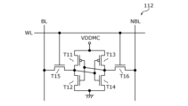
- FIG. 3 is a circuit diagram of a memory cell according to Embodiment 1.
- FIG. 4 is a timing chart regarding the power supply control circuit according to the first embodiment.
- FIG. 5 is a diagram showing a configuration of a modification of the power supply control circuit according to the first embodiment.
- FIG. 6 is a timing chart regarding a modification of the power supply control circuit according to the first embodiment.
- FIG. 7 is a block diagram of a semiconductor memory device according to a second embodiment.
- FIG. 8 is a diagram showing the configuration of a write assist circuit according to the second embodiment.
- FIG. 9 is a diagram showing the configuration of a column circuit according to the second embodiment.
- FIG. 10 is a timing chart regarding the write assist circuit according to the second embodiment.
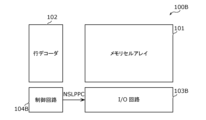
- FIG. 11 is a block diagram of a semiconductor memory device according to a third embodiment.
- FIG. 12 shows a configuration of an I/O circuit according to the third embodiment.
- FIG. 13 is a timing chart regarding the I/O circuit according to the third embodiment.
- 14 is a diagram showing a configuration of Modification 1 of the I/O circuit according to Embodiment 3.
- FIG. FIG. 15 is a timing chart relating to Modification 1 of the I/O circuit of Embodiment 3.
- FIG. FIG. 16 is a diagram showing a configuration of Modification 2 of the I/O circuit according to Embodiment 3. As shown in FIG.
- a semiconductor memory device includes a plurality of memory cells, a first power supply line to which a power supply voltage is supplied, a second power supply line that is a power supply voltage line for the plurality of memory cells, the first a first transistor and a second transistor connected in parallel between a power supply line and the second power supply line; a first mode for supplying the power supply voltage to the plurality of memory cells; Based on a first signal for switching to a second mode in which no power supply voltage is supplied, (i) the first transistor and the second transistor are turned off during the second mode, and a control circuit that turns on the first transistor when switching to the 1 mode, and turns on the second transistor after turning on the first transistor.
- the semiconductor memory device when switching from the second mode to the first mode, by turning on the first transistor and then turning on the second transistor, it is possible to suppress the peak current that accompanies the power restoration. In addition, compared to the case of controlling a plurality of blocks in time series, complication of control can be suppressed.
- the second transistor may have higher driving capability than the first transistor.
- the peak current can be suppressed efficiently.
- control circuit includes a delay circuit that generates a second signal by delaying the first signal, the first signal is supplied to a control terminal of the first transistor, and the control of the second transistor is performed.
- the terminal may be supplied with the second signal.
- the first transistor and the second transistor can be controlled with a simple configuration.
- the semiconductor memory device includes a plurality of memory blocks each including the plurality of memory cells, the first transistor and the second transistor are provided in each of the plurality of memory blocks, and the delay circuit The generated second signal may be supplied to control terminals of two or more of the second transistors provided in two or more of the plurality of memory blocks.
- the delay circuit can be shared by a plurality of memory blocks, so the circuit area can be reduced.
- control circuit detects the voltage of the second power supply line, and detects the voltage of the second power supply line after turning on the first transistor when switching from the second mode to the first mode. reaches a predetermined voltage, the second transistor may be turned on.
- the first transistor and the second transistor can be controlled with high accuracy.
- the semiconductor memory device includes a write assist circuit that lowers the voltage of the second power supply line when writing data to the plurality of memory cells than the voltage of the second power supply line during a period other than when writing data.
- the first transistor and the second transistor may be included in the write assist circuit, and one of the first transistor and the second transistor may be turned off during the data write.
- the transistors used in the write assist circuit can be used as the first transistor and the second transistor, an increase in circuit area can be suppressed.
- a semiconductor memory device includes a plurality of memory cells, a first bit line connected to the plurality of memory cells, a first precharge circuit connected to the first bit line, and (i) the second (ii) when switching from the second mode to the first mode, the first precharge circuit is turned on and the first precharge circuit is turned off; and a control circuit for turning on the second precharge circuit after turning on the charge circuit.
- the semiconductor memory device when switching from the second mode to the first mode, the first precharge circuit is turned on, and then the second precharge circuit is turned on. can be suppressed. In addition, compared to the case of controlling a plurality of blocks in time series, complication of control can be suppressed.
- the second precharge circuit may have higher driving capability than the first precharge circuit.
- the peak current can be suppressed efficiently.
- control circuit includes a delay circuit that generates a second signal by delaying the first signal, the first precharge circuit is switched on and off based on the first signal, and the The second precharge circuit may be switched on and off based on the second signal.
- the first precharge circuit and the second precharge circuit can be controlled with a simple configuration.
- the semiconductor memory device includes a plurality of memory blocks each including the plurality of memory cells, the first precharge circuit and the second precharge circuit are provided in each of the plurality of memory blocks,
- the second signal generated by the delay circuit may be supplied to two or more second precharge circuits provided in two or more of the plurality of memory blocks.
- the delay circuit can be shared by a plurality of memory blocks, so the circuit area can be reduced.
- control circuit detects the voltage of the first bit line, and when switching from the second mode to the first mode, after turning on the first precharge circuit and reaches a predetermined voltage, the second precharge circuit may be turned on.
- the first precharge circuit and the second precharge circuit can be controlled with high accuracy.
- the semiconductor memory device further includes a second bit line connected to the plurality of memory cells, the first precharge circuit has one of a source and a drain connected to the first bit line, and has a gate. connected to the second bit line; and a second transistor having one of a source and a drain connected to the second bit line and a gate connected to the first bit line. .
- the circuit for holding the voltages of the first bit line and the second bit line can also be used as the first precharge circuit, so an increase in circuit area can be suppressed.
- a control method is a control method for a semiconductor memory device including a plurality of memory cells, a first transistor, and a second transistor, wherein power supply voltage is supplied to the plurality of memory cells. and a second mode in which the power supply voltage is not supplied to the plurality of memory cells, wherein the first transistor is in a first period when switching from the second mode to the first mode.
- the power supply voltage is supplied to the plurality of memory cells through the first period, and the power supply voltage is supplied to the plurality of memory cells through the first transistor and the second transistor in a second period after the first period.
- the semiconductor memory device when switching from the second mode to the first mode, the power supply voltage is supplied through the first transistor, and then the power supply voltage is supplied through the first transistor and the second transistor. can suppress the peak current that accompanies power supply recovery. In addition, compared to the case of controlling a plurality of blocks in time series, complication of control can be suppressed.
- a control method is a semiconductor memory device including a plurality of memory cells, bit lines connected to the plurality of memory cells, a first precharge circuit, and a second precharge circuit. comprising a first mode in which the bit line is precharged and a second mode in which the bit line is not precharged, wherein the first mode is switched from the second mode to the first mode. period, the bit line is precharged by the first precharge circuit, and the bit line is precharged by the first precharge circuit and the second precharge circuit in a second period after the first period. .
- the first precharge circuit when switching from the second mode to the first mode, precharges the bit line, and then the first precharge circuit and the second precharge circuit precharge the bit line.
- precharging the bit line it is possible to suppress the peak current that accompanies power supply recovery.
- complication of control can be suppressed.
- the peak current means the maximum value of instantaneously flowing current.
- power supply noise is generated due to an increase in peak current, which increases the possibility of malfunction of other logic circuits and the like.
- FIG. 1 is a block diagram of a semiconductor memory device 100 according to this embodiment.
- This semiconductor memory device 100 is an SRAM and includes a memory cell array 101 , a row decoder 102 , an I/O circuit 103 , a control circuit 104 and a power supply control circuit 105 .
- the semiconductor memory device 100 may be another RAM (Random Access Memory) such as a DRAM (Dynamic Random Access Memory). Also, the semiconductor memory device 100 may be a non-volatile memory such as a flash memory.
- RAM Random Access Memory
- DRAM Dynamic Random Access Memory
- the semiconductor memory device 100 may be a non-volatile memory such as a flash memory.
- the semiconductor memory device 100 is implemented as, for example, an LSI (Large Scale Integrated Circuit), which is an integrated circuit. These may be made into one chip individually, or may be made into one chip so as to include part or all of them. Also, the semiconductor memory device 100 may be one block included in an LSI.
- LSI Large Scale Integrated Circuit
- the memory cell array 101 includes a plurality of memory cells 112 arranged in rows and columns, each holding 1-bit data.
- a row decoder 102 performs row selection of a plurality of memory cells 112 arranged in a matrix.
- the I/O circuit 103 writes data to the memory cell array 101 and reads data held in the memory cell array 101 .
- the power supply control circuit 105 switches whether to supply a power supply voltage (hereinafter also referred to as power supply) to the memory cell array 101 .
- a power supply voltage hereinafter also referred to as power supply
- the semiconductor memory device 100 has at least a power down mode (second mode) in which power is not supplied to the memory cell array 101 and a normal mode (first mode) in which power is supplied to the memory cell array 101 .
- power-down mode power supply to peripheral circuits such as the row decoder 102 and the I/O circuit 103 may not be performed.
- normal mode power is supplied not only to the memory cell array 101 but also to peripheral circuits.
- the semiconductor memory device 100 is in a mode in which power is supplied to the memory cell array 101 but power is not supplied to the peripheral circuits (power is not supplied to the peripheral circuits, but data retention in the memory cell array 101 is continued). mode).
- the control circuit 104 controls each processing unit. Specifically, the control circuit 104 generates a plurality of control signals for controlling each processing unit. The control circuit 104 also generates a signal SDMC for switching between the power down mode and the normal mode, and supplies the generated signal SDMC to the power supply control circuit 105 . For example, control circuit 104 generates signal SDMC based on a signal input from the outside of semiconductor memory device 100 . Control circuit 104 may supply signal SDMC input from the outside of semiconductor memory device 100 to power supply control circuit 105 as it is, or signal SDMC input from the outside of semiconductor memory device 100 may cause control circuit 104 to operate. It may be supplied to the power supply control circuit 105 as it is without passing through.
- FIG. 2 is a diagram showing configurations of the memory cell array 101 and the power supply control circuit 105.
- Memory cell array 101 includes a plurality of memory blocks 111 .
- Each memory block 111 includes multiple memory cells 112 .
- a plurality of memory blocks 111 are formed by dividing the memory cell array 101 in units of multiple columns in the horizontal direction.
- the memory cell array 101 may be divided vertically and horizontally in units of a plurality of columns and a plurality of rows.
- the number of memory cells 112 included in the memory block 111 may be any number.
- the memory cell array 101 does not have to be divided into a plurality of memory blocks 111 .
- Each memory cell 112 is connected to a memory power supply line VDDMC, which is a power supply line for the memory cell 112, and each memory cell 112 is supplied with a power supply voltage via the memory power supply line VDDMC.
- the power supply control circuit 105 includes a delay circuit 121 and a plurality of power supply switching circuits 122 .
- Delay circuit 121 generates signal SDMC2 by delaying signal SDMC.
- the power switching circuit 122 is provided for each memory block 111 and switches whether to supply power to the memory cell array 101 or not.
- the power switching circuit 122 includes a first transistor T01 and a second transistor T02.
- the first transistor T01 is connected between a power supply line VDD supplied with a power supply voltage and a memory power supply line VDDMC.
- the source of the first transistor T01 is connected to the power supply line VDD, and the drain is connected to the memory power supply line VDDMC.
- a signal SDMC is supplied to the gate (control terminal) of the first transistor T01.
- a power supply line VDD is a power supply line for the semiconductor memory device 100, and is applied with a power supply voltage supplied from the outside of the semiconductor memory device 100, for example.
- the second transistor T02 is connected between the power supply line VDD and the memory power supply line VDDMC. Specifically, the source of the second transistor T02 is connected to the power supply line VDD, and the drain is connected to the memory power supply line VDDMC. A signal SDMC2 is supplied to the gate (control terminal) of the second transistor. That is, the first transistor T01 and the second transistor T02 are connected in parallel between the power supply line VDD and the memory power supply line VDDMC.
- the second transistor T02 has higher driving capability than the first transistor T01.
- the drivability is adjusted by, for example, the W/L (gate width/gate length) of the transistor, the threshold voltage of the transistor, or the level of the voltage applied to the gate or source of the transistor.
- the driving ability of the second transistor T02 may be the same as the driving ability of the first transistor T01, or may be lower than the driving ability of the first transistor T01.
- MOSFETs metal-oxide-semiconductor field-effect transistors
- bipolar transistors other transistors such as bipolar transistors may also be used.
- FIG. 3 is a circuit diagram of the memory cell 112.
- the memory cell 112 is, for example, an SRAM memory cell composed of six transistors T11 to T16 as shown in FIG. are connected to the bit lines BL and NBL. Also, the memory cell 112 is supplied with a power supply voltage through a memory power supply line VDDMC.
- FIG. 4 is a timing chart showing the operation of the semiconductor memory device 100 when the operation mode is switched.
- the signal SDMC is at low level in normal mode and at high level in power down mode.
- the signal SDMC is at low level and the semiconductor memory device 100 operates in the normal mode. Note that a state in which write operation and read operation are not performed in the normal mode is called a standby state.
- the signal SDMC changes from low level to high level, and the operation mode shifts to power down mode.
- the first transistor T01 is turned off.
- the signal SDMC2 becomes high level at time t02 later than the signal SDMC.
- the second transistor T02 is turned off when the signal SDMC2 becomes high level.
- the signal SDMC changes from high level to low level, and the operation mode shifts from power down mode to normal mode.
- the signal SDMC becomes low level, the first transistor T01 is turned on.
- the power supply to the memory power supply line VDDMC is started, and the voltage of the memory power supply line VDDMC starts to rise.
- the signal SDMC2 becomes low level at time t04 after the signal SDMC.
- the second transistor T02 is turned on.
- the first transistor T01 is turned on and the second transistor T02 is not turned on.
- the peak current at the time of switching can be suppressed.
- both the first transistor T01 and the second transistor T02 are turned on, so that sufficient power supply can be realized.
- the solid line indicates the current when the method of the present embodiment is applied
- the dashed line indicates the current (comparative example) when the method of the present embodiment is not applied.
- the semiconductor memory device 100 includes the plurality of memory cells 112, the first power supply line VDD to which the power supply voltage is supplied, and the second power supply line VDD which is the power supply voltage line of the plurality of memory cells 112.
- the power supply control circuit 105 turns off the second transistor T02, (ii) turns on the first transistor T01 when switching from the second mode to the first mode, and turns on the second transistor T02 after turning on the first transistor T01. and
- the semiconductor memory device 100 when switching from the second mode to the first mode, the first transistor T01 is turned on, and then the second transistor T02 is turned on, thereby suppressing the peak current accompanying the power recovery. can. In addition, compared to the case of controlling a plurality of blocks in time series, complication of control can be suppressed.
- the second transistor T02 has higher driving capability than the first transistor T01. According to this, the peak current can be suppressed efficiently.
- the power control circuit 105 includes a delay circuit 121 that delays the first signal SDMC to generate the second signal SDMC2.
- a first signal SDMC is supplied to the control terminal of the first transistor T01, and a second signal SDMC2 is supplied to the control terminal of the second transistor T02. According to this, the first transistor T01 and the second transistor T02 can be controlled with a simple configuration.
- the semiconductor memory device 100 includes multiple memory blocks 111 each including multiple memory cells 112 .
- a first transistor T01 and a second transistor T02 are provided in each of the plurality of memory blocks 111 .
- the second signal SDMC2 generated by the delay circuit 121 is supplied to control terminals of two or more second transistors T02 provided in two or more memory blocks 111 out of the plurality of memory blocks 111 . According to this, since the delay circuit 121 can be shared by a plurality of memory blocks 111, the circuit area can be reduced.
- FIG. 2 illustrates an example in which the signal SDMC2 generated by the delay circuit 121 is supplied to all the second transistors T02 (that is, an example in which all the second transistors T02 share one delay circuit 121).
- a delay circuit 121 is provided for each one or more memory blocks 111 (one or more second transistors T02), and the signal SDMC2 generated by each delay circuit 121 corresponds to the delay circuit 121. may be supplied to one or more second transistors T02 that
- control method of the semiconductor memory device 100 is a control method of the semiconductor memory device 100 including a plurality of memory cells 112, the first transistor T01, and the second transistor T02.
- the control method has a first mode (normal mode) in which power supply voltage is supplied to the plurality of memory cells 112 and a second mode (power down mode) in which power supply voltage is not supplied to the plurality of memory cells 112 .
- first mode normal mode
- second mode power down mode
- the power supply voltage is supplied to the plurality of memory cells 112 via the first transistor T01, A power supply voltage is supplied to the plurality of memory cells 112 via the first transistor T01 and the second transistor T02 in a second period (after t04 in FIG. 4) after one period.
- the power supply voltage is supplied via the first transistor T01, and then via the first transistor T01 and the second transistor T02.
- the peak current associated with power supply recovery can be suppressed.
- complication of control can be suppressed.
- FIG. 5 is a diagram showing the configuration of a power control circuit 105A that is a modification of the power control circuit 105. As shown in FIG. A power control circuit 105A shown in FIG. 5 differs from the power control circuit 105 shown in FIG.
- the voltage detection circuit 123 detects the voltage of the memory power supply line VDDMC, and when the signal SDMC is at the low level (power-down mode) and the voltage of the memory power supply line VDDMC is equal to or higher than a predetermined voltage, the voltage detection circuit 123 detects the voltage of the memory power supply line VDDMC. level, otherwise a signal SDMC3 that is high level is generated.
- the signal SDMC3 is supplied to the gate (control terminal) of the second transistor T02. Note that the circuit configuration of the voltage detection circuit 123 shown in FIG. 5 is an example, and any circuit configuration may be used as long as the circuit configuration can realize a similar function.
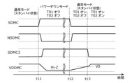
- FIG. 6 is a timing chart showing the operation when switching the operation mode in the modification.
- signal SDMC is at low level and semiconductor memory device 100 operates in the normal mode.
- the signal SDMC changes from low level to high level, and the operation mode shifts to power down mode.
- the first transistor T01 is turned off.
- the signal SDMC3 becomes high level.
- the second transistor T02 is turned off.
- the signal SDMC changes from high level to low level, and the operation mode shifts from power down mode to normal mode.
- the signal SDMC becomes low level, the first transistor T01 is turned on.
- the voltage of the memory power supply line VDDMC rises and reaches the predetermined voltage V0 at time t13.
- the voltage detection circuit 123 detects that the voltage of the memory power supply line VDDMC has reached the voltage V0, and changes the signal SDMC3 to low level.
- the second transistor T02 is turned on.
- the first transistor T01 is turned on and the second transistor T02 is not turned on.
- the peak current at the time of switching can be suppressed.
- both the first transistor T01 and the second transistor T02 are turned on, so that sufficient power supply can be realized.
- the power supply control circuit 105A detects the voltage of the second power supply line VDDMC, and turns on the first transistor T01 when switching from the second mode (power-down mode) to the first mode (normal mode). After that, and when the voltage of the second power supply line VDDMC reaches the predetermined voltage V0, the second transistor T02 is turned on. According to this, the first transistor T01 and the second transistor T02 can be controlled with high accuracy.
- Embodiment 2 In this embodiment mode, an example will be described in which the function of the power supply control circuit 105 described in Embodiment Mode 1 is also used as a write assist circuit that controls the power supply voltage of the memory cell array 101 when data is written.
- FIG. 7 is a block diagram of a semiconductor memory device 100A according to this embodiment.
- Semiconductor memory device 100A shown in FIG. 7 includes write assist circuit 106 instead of power control circuit 105 in semiconductor memory device 100 shown in FIG.
- the write assist circuit 106 is a circuit that makes it easier to write data by lowering the power supply voltage of the memory cell 112 when writing data.
- the write assist circuit 106 has the function of the power supply control circuit 105 described in the first embodiment.
- FIG. 8 is a diagram showing the configuration of the memory cell array 101 and write assist circuit 106.
- FIG. Memory cell array 101 includes a plurality of memory blocks 111 . Each memory block 111 includes multiple memory cells 112 . Here, the memory cell array 101 is divided into memory blocks 111 for each column.
- memory power supply lines VDDMC VDDMC0 to VDDMC7 are provided for each column (for each memory block 111).
- Each memory block 111 is connected to a memory power supply line VDDMC corresponding to the memory block 111, and a power supply voltage is supplied to each memory block 111 through the memory power supply line VDDMC corresponding to the memory block 111.
- the write assist circuit 106 includes a delay circuit 131 and multiple column circuits 132 .
- the delay circuit 131 delays and inverts the signal SDMC to generate the signal NSDMC.
- a column circuit 132 is provided for each column and controls the level of the power supply voltage supplied to the memory cells 112 in each column. Specifically, the column circuit 132 performs control to lower the power supply voltage when writing data. Also, the column circuit 132 performs the same control as in the first embodiment when switching the operation mode.
- FIG. 9 is a diagram showing the configuration of the column circuit 132. As shown in FIG. As shown in FIG. 9, the column circuit 132 includes a logic circuit 141 and transistors T31-T34.
- FIG. 10 is a timing chart showing the operation when switching the operation mode according to the present embodiment.
- the signal SDMC is at low level in normal mode and at high level in power down mode.
- a signal NSWWA is a signal indicating whether or not write assistance is to be performed, and is at low level when write assistance is to be performed, and is at high level when write assistance is not to be performed. In FIG. 10, the signal NSWWA is low and write assist is performed.
- the signal NWCA (NWCA0 to NWCA7) is a signal indicating whether or not it is a write mode for writing data to the memory cell 112, and is low level in the write mode and high level in other than the write mode.
- a signal CLK shown in the figure is a clock signal used for the write operation.
- the signal NSWWA, the signal NWCA and the signal CLK are generated by the control circuit 104, for example. Control circuit 104 may generate at least one of these signals based on a signal input from outside semiconductor memory device 100 .
- control circuit 104 may supply a signal input from the outside of the semiconductor memory device 100 to the write assist circuit 106 as it is, or a signal input from the outside of the semiconductor memory device 100 may Alternatively, it may be supplied to the write assist circuit 106 as it is.
- Logic circuit 141 generates signal WTA based on signal NSDMC and signal NWCA0. Specifically, the logic circuit 141 outputs a high level signal WTA when at least one of the signal NSDMC and the signal NWCA0 is at low level, and otherwise outputs a low level signal WTA.
- the first transistor T31 corresponds to the first transistor T01 according to the first embodiment.
- the first transistor T31 is connected between a power supply line VDD supplied with a power supply voltage and a memory power supply line VDDMC0.
- the source of the first transistor T01 is connected to the power supply line VDD, and the drain is connected to the memory power supply line VDDMC.
- a signal SDMC is supplied to the gate (control terminal) of the first transistor T31.
- the second transistor T32 is connected between the power supply line VDD and the memory power supply line VDDMC0. Specifically, the source of the second transistor T32 is connected to the power supply line VDD, and the drain is connected to the memory power supply line VDDMC0. A signal WTA is supplied to the gate (control terminal) of the second transistor T32. That is, the first transistor T31 and the second transistor T32 are connected in parallel between the power supply line VDD and the memory power supply line VDDMC0.
- the second transistor T32 has a higher driving capability than the first transistor T31.
- the driving ability of the second transistor T32 may be the same as the driving ability of the first transistor T31, or may be lower than the driving ability of the first transistor T31.
- the transistors T33 and T34 are connected in series between the memory power supply line VDDMC0 and the ground line to which the ground potential is supplied.
- a signal NSWWA is supplied to the gate (control unit) of the transistor T33.
- a signal WTA is supplied to the gate (control unit) of the transistor T34.
- the signal SDMC is at low level and the semiconductor memory device 100 operates in the normal mode.
- the signal SDMC changes from low level to high level, and the operation mode shifts to power down mode.
- the signal SDMC becomes high level
- the first transistor T31 is turned off.
- the signal NSDMC becomes low level at time t22 later than the signal SDMC, and the signal WTA becomes high level.
- the second transistor T32 is turned off. By turning off both the first transistor T31 and the second transistor T32, the power supply to the memory cell array 101 is interrupted, and the memory power supply line VDDMC0 becomes Hi-Z state.
- the signal SDMC changes from high level to low level, and the operation mode shifts from power down mode to normal mode.
- the signal SDMC becomes low level, the first transistor T31 is turned on. As a result, power supply to the memory power supply line VDDMC0 is started, and the voltage of the memory power supply line VDDMC0 starts to rise.
- the signal NSDMC becomes high level at time t24 after the signal SDMC, and the signal WTA becomes low level.
- the second transistor T32 is turned on.
- the first transistor T31 is turned on and the second transistor T32 is not turned on. Thereby, the peak current at the time of switching can be suppressed. Moreover, in the period after time t24, both the first transistor T31 and the second transistor T32 are turned on, so that sufficient power supply can be achieved.
- the signal NWCA0 becomes low level and the operation mode shifts to the write mode.
- the signal WTA becomes high level. This turns off the second transistor T32 and turns on the transistor T34.
- the transistor T33 is on, and since the signal SDMC is at low level, the first transistor T31 is on.
- the voltage of the memory power supply line VDDMC0 becomes a voltage corresponding to the ratio between the ON resistance of the first transistor T31 and the ON resistances of the transistors T33 and T34. That is, the voltage of the memory power supply line VDDMC0 is lowered, and write assist is realized.
- the voltage of the second power supply line VDDMC0 when writing data to the plurality of memory cells 112 is set to It includes a write assist circuit 106 that lowers the A first transistor T31 and a second transistor T32 are included in the write assist circuit 106 .
- One of the first transistor T31 and the second transistor T32 is turned off during data writing. According to this, since the transistors used in the write assist circuit 106 can be used as the first transistor T31 and the second transistor T32, an increase in circuit area can be suppressed.
- FIG. 11 is a block diagram of a semiconductor memory device 100B according to this embodiment. Unlike the semiconductor memory device 100 shown in FIG. 1, the semiconductor memory device 100B shown in FIG. 104 different.
- the semiconductor memory device 100B also has a power-down mode (second mode) in which bit lines are not precharged, and a normal mode (first mode) in which bit lines are precharged.
- power-down mode power may not be supplied to circuits other than precharge-related circuits included in the row decoder 102 and the I/O circuit 103B. Power is also supplied to these circuits in the normal mode.
- power down mode power may or may not be supplied to the memory cell array 101 .
- the semiconductor memory device 100B may have a mode in which power is supplied to the memory cell array 101 and a mode in which power is not supplied to the memory cell array 101 while power is not supplied to the peripheral circuit.
- the control circuit 104B generates a signal NSLPPC for switching between the power down mode and the normal mode, and supplies the generated signal NSLPPC to the I/O circuit 103B.
- control circuit 104B generates signal NSLPPC based on a signal input from the outside of semiconductor memory device 100B.
- Control circuit 104B may directly supply signal NSLPPC input from outside semiconductor memory device 100B to I/O circuit 103B, or signal NSLPPC input from outside semiconductor memory device 100B may be supplied to control circuit 104B. It may be supplied to the I/O circuit 103B as it is without passing through.
- FIG. 12 is a diagram showing configurations of the memory cell array 101 and the I/O circuit 103B. Note that FIG. 1 shows a circuit configuration corresponding to one column of the memory cell array 101, and the configuration shown in FIG. 12 is provided for each column. In the configuration shown in FIG. 12, the precharge control circuit 151 may be provided as a circuit common to multiple columns.
- a plurality of memory cells 112 are connected to a pair of bit lines BL and NBL provided for each column.
- the I/O circuit 103B includes a precharge control circuit 151, a first precharge circuit 152, a second precharge circuit 153, a write driver 154, a sense amplifier 155, and transistors T46 and T47.
- the precharge control circuit 151 generates a signal Y for controlling on/off of the first precharge circuit 152 and a signal Z for controlling on/off of the second precharge circuit 153 based on the signal NSLPPC and the signal NPC. do.
- Precharge control circuit 151 includes delay circuit 156 and logic circuits 157 and 158 .
- the signal NSLPPC is at high level in normal mode and at low level in power down mode.
- the signal NPC is a signal indicating whether or not to perform precharging, and is high level when precharging is performed (during standby), and is low level when precharging is not performed (during reading and writing).
- a signal NRCA is an address selection signal, which is at a low level during reading and at a high level otherwise.
- the delay circuit 156 generates the signal X by delaying the signal NSLPPC.
- the logic circuit 157 is a NAND circuit, and outputs a high level signal Y when at least one of the signal NSLPPC and the signal NPC is low level, and outputs a low level signal Y otherwise.
- the logic circuit 158 is a NAND circuit, and outputs a high level signal Z when at least one of the signal X and the signal NPC is low level, and outputs a low level signal Z otherwise.
- the first precharge circuit 152 is a circuit that precharges the bit lines BL and NBL, precharges the bit lines BL and NBL when the signal Y is at low level, and precharges the bit lines when the signal Y is at high level. Do not precharge BL and NBL.
- This first precharge circuit 152 includes transistors T41 and T42.
- the transistor T41 is connected between the power supply line VDD to which the power supply voltage is supplied and the bit line BL. Specifically, the source of the transistor T41 is connected to the power supply line VDD, and the drain is connected to the bit line BL. A signal Y is supplied to the gate (control terminal) of the transistor T41.
- a power supply line VDD is a power supply line for the semiconductor memory device 100B, and is applied with a power supply voltage supplied from the outside of the semiconductor memory device 100B, for example.
- the transistor T42 is connected between the power supply line VDD and the bit line NBL. Specifically, the source of the transistor T42 is connected to the power supply line VDD, and the drain is connected to the bit line NBL. A signal Y is supplied to the gate (control terminal) of the transistor T42.
- the second precharge circuit 153 is a circuit that precharges the bit lines BL and NBL, precharges the bit lines BL and NBL when the signal Z is at low level, and precharges the bit lines when the signal Z is at high level. Do not precharge BL and NBL.
- This second precharge circuit 153 includes transistors T43, T44 and T45.
- the transistor T43 is connected between the power supply line VDD and the bit line BL. Specifically, the source of the transistor T43 is connected to the power supply line VDD, and the drain is connected to the bit line BL. A signal Z is supplied to the gate (control terminal) of the transistor T43. That is, the transistors T41 and T43 are connected in parallel between the power supply line VDD and the bit line BL.
- the transistor T44 is connected between the power supply line VDD and the bit line NBL. Specifically, the source of the transistor T44 is connected to the power supply line VDD, and the drain is connected to the bit line NBL. A signal Z is supplied to the gate (control terminal) of the transistor T44. That is, the transistors T42 and T44 are connected in parallel between the power supply line VDD and the bit line NBL.
- the transistor T45 is connected between the bit line BL and the bit line NBL.
- a signal Z is supplied to the gate (control terminal) of the transistor T45.
- the transistors T43 and T44 have a higher driving capability than the transistors T41 and T42.
- the drivability is adjusted by, for example, the W/L (gate width/gate length) of the transistor, the threshold voltage of the transistor, or the level of the voltage applied to the gate or source of the transistor.
- the driving capabilities of the transistors T43 and T44 may be the same as the driving capabilities of the transistors T41 and T42, or may be lower than the driving capabilities of the transistors T41 and T42.
- the write driver 154 drives the bit lines BL and NBL according to write data during writing.
- the sense amplifier 155 detects the voltages of the bit lines BL and NBL during reading, and generates read data corresponding to the voltages.
- Transistors T46 and T47 are connected between bit lines BL and NBL and sense amplifier 155 .
- FIG. 13 is a timing chart showing the operation when switching the operation mode in semiconductor memory device 100B.
- the signal NSLPPC is at high level and the semiconductor memory device 100B operates in the normal mode.
- signal NSLPPC changes from high level to low level, and the operation mode shifts to power down mode.
- the signal NSLPPC becomes low level, the signal Y becomes high level.
- the first precharge circuit 152 is turned off. That is, the transistors T41 and T42 are turned off.
- the signal Z becomes high level at time t32.
- the second precharge circuit 153 is turned off when the signal Z becomes high level. That is, the transistors T43, T44 and T45 are turned off.
- bit lines BL and NBL are not precharged, and the bit lines BL and NBL are in the Hi-Z state.
- the signal NSLPPC changes from low level to high level, and the operation mode shifts from power down mode to normal mode.
- the signal NSLPPC becomes high level
- the signal Y becomes low level.
- the first precharge circuit 152 is turned on. That is, the transistors T41 and T42 are turned on.
- voltage supply (precharge) to the bit lines BL and NBL is started, and the voltages of the bit lines BL and NBL start to rise.
- the signal Z becomes low level at time t34.
- the second precharge circuit 153 is turned on. That is, the transistors T43, T44 and T45 are turned on.
- the first precharge circuit 152 is turned on and the second precharge circuit 153 is not turned on during the period t33 to t34 when switching from the power down mode to the normal mode. Thereby, the peak current at the time of switching can be suppressed. Moreover, in the period after time t34, both the first precharge circuit 152 and the second precharge circuit 153 are turned on, so that sufficient voltage supply can be realized.
- Modification 1 of the I/O circuit 103B will be described below.
- the precharge circuit is switched on/off by controlling the gate of the transistor included in the precharge circuit. ON/OFF of the precharge circuit is switched by switching .
- FIG. 14 is a diagram showing the configuration of an I/O circuit 103C, which is a modification of the I/O circuit 103B.
- the I/O circuit 103C has a precharge control circuit 151A, a first precharge circuit 152A, and a second precharge circuit 153A, which are different from the I/O circuit 103B. It differs from the configuration of the charge circuit 152 and the second precharge circuit 153 .
- the precharge control circuit 151A may be provided as a circuit common to multiple columns.
- the precharge control circuit 151A generates a signal NY for controlling on/off of the first precharge circuit 152A and a signal NZ for controlling on/off of the second precharge circuit 153A based on the signal NSLPPC.
- the precharge control circuit 151A includes inverters 161 and 163, a delay circuit 162, and transistors T61 and T62.
- the inverter 161 generates the signal A by inverting the signal NSLPPC.
- Delay circuit 162 generates signal X by delaying signal A.
- FIG. Inverter 163 generates signal B by inverting signal NPC.
- the transistor T61 is connected between the power supply line VDD and the bit lines BL and NBL. Specifically, the transistor T61 is connected to the bit line BL through the transistor T51, and is connected to the bit line NBL through the transistor T52. In other words, the transistor T61 switches whether to supply the power supply voltage to the first precharge circuit 152A based on the signal A (signal NSLPPC). Specifically, the source of the transistor T61 is connected to the power supply line VDD, and the drain is connected to the power supply line NY. A signal A is supplied to the gate (control terminal) of the transistor T61.
- the transistor T62 is connected between the power supply line VDD and the bit lines BL and NBL. Specifically, the transistor T62 is connected to the bit line BL via the transistor T53, and is connected to the bit line NBL via the transistor T54. In other words, the transistor T62 switches based on the signal X whether to supply the power supply voltage to the second precharge circuit 153A. Specifically, the source of the transistor T62 is connected to the power supply line VDD, and the drain is connected to the power supply line NZ. A signal X is supplied to the gate (control terminal) of the transistor T62. That is, the transistors T61 and T62 are connected in parallel between the power supply line VDD and the bit lines BL and NBL.
- the transistor T62 has a higher driving capability than the transistor T61.
- the driving capability is adjusted by, for example, the W/L (gate width/gate length) of the transistor, the threshold voltage, or the voltage level applied to the gate or source.
- the driving ability of the transistor T62 may be the same as the driving ability of the transistor T61, or may be lower than the driving ability of the transistors T51 and T52.
- the first precharge circuit 152A is a circuit that precharges the bit lines BL and NBL.
- the first precharge circuit 152A includes transistors T51 and T52.
- the transistor T51 is connected between the power supply line NY and the bit line BL. Specifically, the source of the transistor T51 is connected to the power supply line NY, and the drain is connected to the bit line BL. A signal B is supplied to the gate (control terminal) of the transistor T51.
- the transistor T52 is connected between the power supply line NY and the bit line NBL. Specifically, the source of the transistor T52 is connected to the power supply line NY, and the drain is connected to the bit line NBL. A signal B is supplied to the gate (control terminal) of the transistor T52.
- the second precharge circuit 153A is a circuit that precharges the bit lines BL and NBL.
- the second precharge circuit 153A includes transistors T53 and T54 and a transistor T55.
- the transistor T53 is connected between the power supply line NZ and the bit line BL. Specifically, the source of the transistor T53 is connected to the power supply line NZ, and the drain is connected to the bit line BL. A signal B is supplied to the gate (control terminal) of the transistor T53.
- the transistor T54 is connected between the power supply line NZ and the bit line NBL. Specifically, the source of the transistor T54 is connected to the power supply line NZ, and the drain is connected to the bit line NBL. A signal B is supplied to the gate (control terminal) of the transistor T54.
- the transistor T55 is connected between the bit line BL and the bit line NBL.
- a signal B is supplied to the gate (control terminal) of the transistor T55.
- the transistors T53 and T54 have a higher driving capability than the transistors T51 and T52.
- the driving capabilities of the transistors T53 and T54 may be the same as the driving capabilities of the transistors T51 and T52, or may be lower than the driving capabilities of the transistors T51 and T52.
- FIG. 15 is a timing chart showing the operation at the time of switching the operation mode in Modification 1.
- the signal NSLPPC is at high level and the semiconductor memory device 100B operates in the normal mode.
- the signal NSLPPC changes from high level to low level, and the operation mode shifts to the power down mode.
- the signal NSLPPC becomes low level, the signal A becomes high level. This turns off the transistor T61.
- the signal X becomes high level at time t42, later than the signal A.
- the transistor T62 is turned off by the signal X becoming high level.
- the power supply to the first precharge circuit 152A and the second precharge circuit 153A is cut off, and the first precharge circuit 152A and the second precharge circuit 153A are turned off. Therefore, the bit lines BL and NBL are not precharged, and the bit lines BL and NBL are in the Hi-Z state.
- the signal NSLPPC changes from low level to high level, and the operation mode shifts from power down mode to normal mode.
- the signal NSLPPC becomes high level
- the signal A becomes low level.
- the transistor T61 is turned on, and the voltage of the power supply line NY begins to rise.
- the first precharge circuit 152A is turned on, and precharging of the bit lines BL and NBL by the first precharge circuit 152A is started, whereby the voltages of the bit lines BL and NBL start to rise. Also, voltage is supplied from the bit lines BL and NBL to the power line NZ through the second precharge circuit 153A, and the voltage of the power line NZ rises.
- the signal X becomes low level at time t44, later than the signal A.
- the transistor T62 is turned on, and power is supplied from the power supply line VDD to the second precharge circuit 153A.
- the second precharge circuit 153A is turned on, and the bit lines BL and NBL are precharged by the first precharge circuit 152A and the second precharge circuit 153A.
- the transistor T61 is turned on and the transistor T62 is not turned on. That is, the first precharge circuit 152A is turned on, and the second precharge circuit 153A is not turned on. Thereby, the peak current at the time of switching can be suppressed. Also, in the period after time t44, both the first precharge circuit 152A and the second precharge circuit 153A are turned on by turning on both the transistor T61 and the transistor T62. Thereby, a voltage supply with sufficient capacity can be realized.
- the semiconductor memory device 100B includes a plurality of memory cells 112, and the first precharge circuit 152 and the second precharge circuit 153 (or the first precharge circuit 153) connected to the first bit line BL.
- precharge circuit 152A and second precharge circuit 153A precharge circuit 152A and second precharge circuit 153A
- first mode normal mode
- second mode power-down mode
- first bit lines BL are not precharged.
- in the second mode turn off the first precharge circuit 152 and the second precharge circuit 153; and
- a precharge control circuit 151 (or a precharge control circuit 151A) that turns on the first precharge circuit 152 and turns on the second precharge circuit 153 after turning on the first precharge circuit 152 .
- the semiconductor memory device 100B when switching from the second mode to the first mode, the first precharge circuit 152 is turned on, and then the second precharge circuit 153 is turned on. Peak current can be suppressed. In addition, compared to the case of controlling a plurality of blocks in time series, complication of control can be suppressed.
- the second precharge circuit 153 has a higher driving capability than the first precharge circuit 152. According to this, the peak current can be suppressed efficiently.
- the precharge control circuit 151 includes a delay circuit 156 (or a delay circuit 162) that generates the second signal X by delaying the first signal NSLPPC.
- the first precharge circuit 152 is switched on and off based on the first signal NSLPPC (eg, signal Y based on the first signal NSLPPC).
- the second precharge circuit 153 is switched on and off based on the second signal X (the signal Z based on the second signal X). According to this, the first precharge circuit 152 and the second precharge circuit 153 can be controlled with a simple configuration.
- the semiconductor memory device 100B includes multiple memory blocks each including multiple memory cells 112 (for example, multiple memory cells 112 for each column).
- a first precharge circuit 152 and a second precharge circuit 153 are provided in each of a plurality of memory blocks (eg columns).
- the second signal X generated by the delay circuit 156 (for example, the signal Z based on the second signal X) is supplied to two or more second precharge circuits 153 provided in two or more of the plurality of memory blocks. Supplied to the control terminal. That is, the delay circuit 156 is shared by multiple columns, for example. According to this, the delay circuit 156 can be shared by a plurality of memory blocks, so that the circuit area can be reduced.
- the circuits shown in FIGS. 12 and 14 are configured to generate a control signal using a delay circuit, like the circuit shown in FIG. circuit may be applied.
- the precharge control circuit 151 has, instead of the delay circuit 156, a voltage detection circuit that detects whether the voltage of the bit line BL or bit line NBL is equal to or higher than a predetermined voltage. .
- the precharge control circuit 151 turns on the second precharge circuit 153 when the signal NSLPPC is at high level and the voltage of the bit line BL or the bit line NBL is equal to or higher than a predetermined voltage.
- Any configuration can be used as such a voltage detection circuit.
- a comparator such as an operational amplifier that compares the reference voltage and the voltage of the bit line BL may be used.
- the precharge control circuit 151 detects the voltage of the first bit line BL, and when switching from the second mode to the first mode, after turning on the first precharge circuit 152 and reaches a predetermined voltage, the second precharge circuit 153 is turned on. According to this, the first precharge circuit 152 and the second precharge circuit 153 can be controlled with high precision.
- control method of the semiconductor memory device 100B is a semiconductor device including a plurality of memory cells 112, bit lines BL connected to the plurality of memory cells 112, a first precharge circuit 152, and a second precharge circuit 153.
- a control method for a storage device 100B which has a first mode (normal mode) in which bit lines BL are precharged and a second mode (power-down mode) in which bit lines BL are not precharged, and from the second mode During the first period (for example, t33 to t34 in FIG. 13) when switching to the first mode, the bit line BL is precharged by the first precharge circuit 152, and the second period after the first period (for example, after t34). ), the bit line BL is precharged by the first precharge circuit 152 and the second precharge circuit 153 .
- the first precharge circuit 152 precharges the bit line BL.
- the peak current associated with power supply recovery can be suppressed.
- complication of control can be suppressed.
- FIG. 16 shows the configuration of an I/O circuit 103D that is a modification of the I/O circuit 103C. Compared to the I/O circuit 103C, the I/O circuit 103D differs from the first precharge circuit 152A in the configuration of the first precharge circuit 152B.
- the first precharge circuit 152B is also used as a cross latch circuit for holding the voltage of the bit line on the higher voltage side of the bit lines BL and NBL during writing.
- the first precharge circuit 152B includes transistors T71 and T72.
- the transistor T71 has a gate connected to the bit line NBL, a source connected to the power supply line NY, and a drain connected to the bit line BL.
- the transistor T72 has a gate connected to the bit line BL, a source connected to the power supply line NY, and a drain connected to the bit line NBL.
- the semiconductor memory device 100B further includes the second bit lines NBL connected to the plurality of memory cells 112.
- the first precharge circuit 152B includes a first transistor T71 having one of its source and drain connected to the first bit line BL and having its gate connected to the second bit line NBL, and one of its source and drain connected to the second bit line. and a second transistor T72 connected to NBL and having a gate connected to the first bit line BL. According to this, since the first precharge circuit 152B can also serve as a circuit for holding the voltages of the first bit line BL and the second bit line NBL, an increase in circuit area can be suppressed.
- the semiconductor memory device is typically realized as an LSI, which is an integrated circuit. These may be made into one chip individually, or may be made into one chip so as to include part or all of them.
- circuit integration is not limited to LSIs, and may be realized with dedicated circuits or general-purpose processors.
- An FPGA Field Programmable Gate Array
- a reconfigurable processor that can reconfigure the connections and settings of the circuit cells inside the LSI may be used.
- the present disclosure may be implemented as a control method for controlling a semiconductor memory device.
- the division of functional blocks in the block diagram is an example, and a plurality of functional blocks can be realized as one functional block, one functional block can be divided into a plurality of functional blocks, and some functions can be moved to other functional blocks.
- single hardware or software may process the functions of a plurality of functional blocks having similar functions in parallel or in a time-sharing manner.
- the present disclosure also includes a circuit capable of realizing the characteristic functions of the present disclosure, as well as the circuit configuration described above.
- the present disclosure also includes devices in which elements such as switching elements (transistors), resistive elements, or capacitive elements are connected in series or parallel to a certain element within the range that can achieve the same function as the above circuit configuration.
- elements such as switching elements (transistors), resistive elements, or capacitive elements are connected in series or parallel to a certain element within the range that can achieve the same function as the above circuit configuration.
- the term “connected” in the above embodiments is not limited to the case where two terminals (nodes) are directly connected, but the two terminals (nodes) can be connected to the extent that the same function can be realized. nodes) are connected via elements.
- the numbers used above are all examples for specifically explaining the disclosure, and the present disclosure is not limited to the numbers exemplified.
- the logic levels represented by high/low or the switching states represented by on/off are examples for concretely describing the present disclosure, and different combinations of the illustrated logic levels or switching states may be used. It is also possible to obtain equivalent results by
- the configuration of the logic circuit shown above is an example for specifically explaining the present disclosure, and it is possible to achieve the same input/output relationship with logic circuits having different configurations.
- the n-type and p-type of transistors and the like are exemplified to specifically describe the present disclosure, and equivalent results can be obtained by inverting these.
- the present disclosure can be applied to semiconductor memory devices.
Landscapes
- Engineering & Computer Science (AREA)
- Power Engineering (AREA)
- Microelectronics & Electronic Packaging (AREA)
- Computer Hardware Design (AREA)
- Static Random-Access Memory (AREA)
Priority Applications (3)
| Application Number | Priority Date | Filing Date | Title |
|---|---|---|---|
| CN202280080399.1A CN118355443A (zh) | 2021-12-08 | 2022-11-24 | 半导体存储装置以及控制方法 |
| JP2023566218A JPWO2023106105A1 (https=) | 2021-12-08 | 2022-11-24 | |
| US18/670,302 US20240304222A1 (en) | 2021-12-08 | 2024-05-21 | Semiconductor memory device and control method |
Applications Claiming Priority (2)
| Application Number | Priority Date | Filing Date | Title |
|---|---|---|---|
| JP2021199650 | 2021-12-08 | ||
| JP2021-199650 | 2021-12-08 |
Related Child Applications (1)
| Application Number | Title | Priority Date | Filing Date |
|---|---|---|---|
| US18/670,302 Continuation US20240304222A1 (en) | 2021-12-08 | 2024-05-21 | Semiconductor memory device and control method |
Publications (1)
| Publication Number | Publication Date |
|---|---|
| WO2023106105A1 true WO2023106105A1 (ja) | 2023-06-15 |
Family
ID=86730412
Family Applications (1)
| Application Number | Title | Priority Date | Filing Date |
|---|---|---|---|
| PCT/JP2022/043303 Ceased WO2023106105A1 (ja) | 2021-12-08 | 2022-11-24 | 半導体記憶装置及び制御方法 |
Country Status (5)
| Country | Link |
|---|---|
| US (1) | US20240304222A1 (https=) |
| JP (1) | JPWO2023106105A1 (https=) |
| CN (1) | CN118355443A (https=) |
| TW (1) | TW202324410A (https=) |
| WO (1) | WO2023106105A1 (https=) |
Citations (2)
| Publication number | Priority date | Publication date | Assignee | Title |
|---|---|---|---|---|
| US20080056048A1 (en) * | 2006-09-06 | 2008-03-06 | Dong-Wook Seo | Power gating circuit, system on chip circuit including the same and power gating method |
| JP2010198718A (ja) * | 2009-01-29 | 2010-09-09 | Fujitsu Semiconductor Ltd | 半導体記憶装置、半導体装置及び電子機器 |
Family Cites Families (6)
| Publication number | Priority date | Publication date | Assignee | Title |
|---|---|---|---|---|
| US7227804B1 (en) * | 2004-04-19 | 2007-06-05 | Cypress Semiconductor Corporation | Current source architecture for memory device standby current reduction |
| KR100610021B1 (ko) * | 2005-01-14 | 2006-08-08 | 삼성전자주식회사 | 반도체 메모리 장치에서의 비트라인 전압 공급회로와 그에따른 비트라인 전압 인가방법 |
| US7489167B2 (en) * | 2006-04-26 | 2009-02-10 | Infineon Technologies Ag | Voltage detection and sequencing circuit |
| US7751267B2 (en) * | 2007-07-24 | 2010-07-06 | International Business Machines Corporation | Half-select compliant memory cell precharge circuit |
| JP2011123970A (ja) * | 2009-12-14 | 2011-06-23 | Renesas Electronics Corp | 半導体記憶装置 |
| GB2500907B (en) * | 2012-04-04 | 2016-05-25 | Platipus Ltd | Static random access memory devices |
-
2022
- 2022-11-23 TW TW111144814A patent/TW202324410A/zh unknown
- 2022-11-24 JP JP2023566218A patent/JPWO2023106105A1/ja active Pending
- 2022-11-24 CN CN202280080399.1A patent/CN118355443A/zh active Pending
- 2022-11-24 WO PCT/JP2022/043303 patent/WO2023106105A1/ja not_active Ceased
-
2024
- 2024-05-21 US US18/670,302 patent/US20240304222A1/en active Pending
Patent Citations (2)
| Publication number | Priority date | Publication date | Assignee | Title |
|---|---|---|---|---|
| US20080056048A1 (en) * | 2006-09-06 | 2008-03-06 | Dong-Wook Seo | Power gating circuit, system on chip circuit including the same and power gating method |
| JP2010198718A (ja) * | 2009-01-29 | 2010-09-09 | Fujitsu Semiconductor Ltd | 半導体記憶装置、半導体装置及び電子機器 |
Also Published As
| Publication number | Publication date |
|---|---|
| JPWO2023106105A1 (https=) | 2023-06-15 |
| US20240304222A1 (en) | 2024-09-12 |
| TW202324410A (zh) | 2023-06-16 |
| CN118355443A (zh) | 2024-07-16 |
Similar Documents
| Publication | Publication Date | Title |
|---|---|---|
| US10902893B2 (en) | Negative bitline write assist circuit and method for operating the same | |
| KR101296001B1 (ko) | 메모리 어레이를 위한 동적인 누설 제어 | |
| JP4171201B2 (ja) | 半導体記憶装置 | |
| US9087564B2 (en) | Semiconductor storage having different operation modes | |
| CN102301424A (zh) | 具有负电压写入辅助电路的存储器及其方法 | |
| US9990985B1 (en) | Memory device with determined time window | |
| US20150364184A1 (en) | Static random access memory and riving method thereof | |
| US20030198120A1 (en) | Multi-port memory circuit | |
| US8773933B2 (en) | Techniques for accessing memory cells | |
| US8279692B2 (en) | Semiconductor device having hierarchical data line structure and control method thereof | |
| KR20140024817A (ko) | 반도체 기억 장치 및 반도체 기억 장치의 제어 방법 | |
| US20170243634A1 (en) | Semiconductor memory device including sram cells | |
| JP2006059490A (ja) | 半導体記憶装置 | |
| US20150036419A1 (en) | Semiconductor apparatus and data reading method | |
| WO2023106105A1 (ja) | 半導体記憶装置及び制御方法 | |
| US10153036B2 (en) | Method for autocorrective writing to a multiport static random access memory device, and corresponding device | |
| CN107636760B (zh) | 用于双端口存储器的读写装置和方法 | |
| US11189342B2 (en) | Memory macro and method of operating the same | |
| JP2011159332A (ja) | 半導体記憶装置 | |
| US6212116B1 (en) | Semiconductor memory device | |
| US10720194B2 (en) | Semiconductor memory device and data writing method | |
| JP6578655B2 (ja) | 半導体装置 | |
| JP3162783B2 (ja) | 半導体記憶装置 | |
| JP2011159331A (ja) | 半導体記憶装置 | |
| JPH0684366A (ja) | 半導体記憶装置 |
Legal Events
| Date | Code | Title | Description |
|---|---|---|---|
| 121 | Ep: the epo has been informed by wipo that ep was designated in this application |
Ref document number: 22904036 Country of ref document: EP Kind code of ref document: A1 |
|
| ENP | Entry into the national phase |
Ref document number: 2023566218 Country of ref document: JP Kind code of ref document: A |
|
| WWE | Wipo information: entry into national phase |
Ref document number: 202280080399.1 Country of ref document: CN |
|
| NENP | Non-entry into the national phase |
Ref country code: DE |
|
| 122 | Ep: pct application non-entry in european phase |
Ref document number: 22904036 Country of ref document: EP Kind code of ref document: A1 |