WO2023100853A1 - 配線基板、電子装置及び電子モジュール - Google Patents
配線基板、電子装置及び電子モジュール Download PDFInfo
- Publication number
- WO2023100853A1 WO2023100853A1 PCT/JP2022/043914 JP2022043914W WO2023100853A1 WO 2023100853 A1 WO2023100853 A1 WO 2023100853A1 JP 2022043914 W JP2022043914 W JP 2022043914W WO 2023100853 A1 WO2023100853 A1 WO 2023100853A1
- Authority
- WO
- WIPO (PCT)
- Prior art keywords
- conductor
- line
- via conductor
- line conductor
- electrode
- Prior art date
- Legal status (The legal status is an assumption and is not a legal conclusion. Google has not performed a legal analysis and makes no representation as to the accuracy of the status listed.)
- Ceased
Links
Images



















Classifications
-
- H—ELECTRICITY
- H05—ELECTRIC TECHNIQUES NOT OTHERWISE PROVIDED FOR
- H05K—PRINTED CIRCUITS; CASINGS OR CONSTRUCTIONAL DETAILS OF ELECTRIC APPARATUS; MANUFACTURE OF ASSEMBLAGES OF ELECTRICAL COMPONENTS
- H05K1/00—Printed circuits
- H05K1/02—Details
- H05K1/03—Use of materials for the substrate
- H05K1/0306—Inorganic insulating substrates, e.g. ceramic, glass
-
- H—ELECTRICITY
- H05—ELECTRIC TECHNIQUES NOT OTHERWISE PROVIDED FOR
- H05K—PRINTED CIRCUITS; CASINGS OR CONSTRUCTIONAL DETAILS OF ELECTRIC APPARATUS; MANUFACTURE OF ASSEMBLAGES OF ELECTRICAL COMPONENTS
- H05K1/00—Printed circuits
- H05K1/02—Details
-
- H—ELECTRICITY
- H05—ELECTRIC TECHNIQUES NOT OTHERWISE PROVIDED FOR
- H05K—PRINTED CIRCUITS; CASINGS OR CONSTRUCTIONAL DETAILS OF ELECTRIC APPARATUS; MANUFACTURE OF ASSEMBLAGES OF ELECTRICAL COMPONENTS
- H05K3/00—Apparatus or processes for manufacturing printed circuits
- H05K3/40—Forming printed elements for providing electric connections to or between printed circuits
- H05K3/4038—Through-connections; Vertical interconnect access [VIA] connections
-
- H—ELECTRICITY
- H05—ELECTRIC TECHNIQUES NOT OTHERWISE PROVIDED FOR
- H05K—PRINTED CIRCUITS; CASINGS OR CONSTRUCTIONAL DETAILS OF ELECTRIC APPARATUS; MANUFACTURE OF ASSEMBLAGES OF ELECTRICAL COMPONENTS
- H05K3/00—Apparatus or processes for manufacturing printed circuits
- H05K3/46—Manufacturing multilayer circuits
-
- H—ELECTRICITY
- H05—ELECTRIC TECHNIQUES NOT OTHERWISE PROVIDED FOR
- H05K—PRINTED CIRCUITS; CASINGS OR CONSTRUCTIONAL DETAILS OF ELECTRIC APPARATUS; MANUFACTURE OF ASSEMBLAGES OF ELECTRICAL COMPONENTS
- H05K3/00—Apparatus or processes for manufacturing printed circuits
- H05K3/46—Manufacturing multilayer circuits
- H05K3/4644—Manufacturing multilayer circuits by building the multilayer layer by layer, i.e. build-up multilayer circuits
-
- H—ELECTRICITY
- H10—SEMICONDUCTOR DEVICES; ELECTRIC SOLID-STATE DEVICES NOT OTHERWISE PROVIDED FOR
- H10W—GENERIC PACKAGES, INTERCONNECTIONS, CONNECTORS OR OTHER CONSTRUCTIONAL DETAILS OF DEVICES COVERED BY CLASS H10
- H10W70/00—Package substrates; Interposers; Redistribution layers [RDL]
- H10W70/60—Insulating or insulated package substrates; Interposers; Redistribution layers
Definitions
- the present disclosure relates to wiring boards, electronic devices, and electronic modules.
- Japanese Unexamined Patent Application Publication No. 2009-212400 discloses a wiring board having signal lines extending from one substrate surface to the other substrate surface.
- a wiring board includes: an insulating substrate; a first line and a second line located on the insulating substrate and adjacent to each other; a ground film conductor and a ground via conductor located on the insulating substrate and surrounding the first line and the second line; with
- the first line is a first line conductor, a first via conductor connected to the first line conductor, and a side connected to the first via conductor and opposite to the first line conductor with the first via conductor interposed therebetween when seen from above and a second via conductor connected to the second line conductor and extending to a layer different from the layer in which the first via conductor is located;
- the second line is a third line conductor, a third via conductor connected to the third line conductor, and a side connected to the third via conductor and opposite to the third line conductor with the third via conductor interposed therebetween when seen from above and a fourth via conductor connected to the fourth line conductor and extending to a layer different from the layer in which the third via conductor is located;
- An electronic device includes: the above wiring board; an electronic element mounted on the wiring board; Prepare.
- An electronic module includes: the electronic device described above; a module substrate on which the electronic device is mounted; Prepare.
- FIG. 1 is a plan perspective view of a wiring board according to Embodiment 1 of the present disclosure
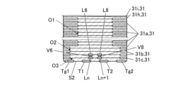
- FIG. 1 is a longitudinal sectional view of a wiring board according to Embodiment 1 of the present disclosure, cut along a signal line
- FIG. FIG. 2 is a plan perspective view of a main part of the wiring board according to Embodiment 1 as seen through from above
- FIG. 3 is a cross-sectional view showing a third layer in the main part of FIG. 2
- FIG. 3 is a cross-sectional view showing a fourth layer in the main part of FIG. 2
- FIG. 3 is a cross-sectional view showing fifth to tenth layers in the main part of FIG. 2
- FIG. 3 is a cross-sectional view showing an eleventh layer in the main part of FIG.
- FIG. 3B is a longitudinal cross-sectional view taken along line AA of FIG. 3B;
- FIG. 3B is a vertical cross-sectional view taken along line BB of FIG. 3B;
- FIG. 5B is a vertical cross-sectional view taken along line CC of FIG. 5A;
- FIG. 3B is a longitudinal cross-sectional view taken along line AA of FIG. 3B;
- FIG. 3B is a vertical cross-sectional view taken along line BB of FIG. 3B;
- FIG. 5B is a vertical cross-sectional view taken along line CC of FIG. 5A
- FIG. 8B is a cross-sectional view showing the fourth layer in the main part of FIG. 8A;
- FIG. 8B is a cross-sectional view showing fifth to ninth layers in the main part of FIG. 8A;
- FIG. 8B is a cross-sectional view showing the tenth layer in the main part of FIG. 8A;
- FIG. 8B is a cross-sectional view showing the eleventh layer in the main part of FIG. 8A;
- FIG. 8B is a cross-sectional view showing the twelfth layer in the main part of FIG. 8A;
- FIG. 8B is a cross-sectional view showing the thirteenth layer in the main part of FIG. 8A;
- FIG. 8B is a cross-sectional view showing the 14th layer in the main part of FIG.
- FIG. 9B is a longitudinal cross-sectional view taken along line AA of FIG. 9B;
- FIG. 9B is a vertical cross-sectional view taken along line BB of FIG. 9B;
- FIG. 10C is a vertical cross-sectional view taken along line CC of FIG. 10C;
- FIG. 10C is a longitudinal cross-sectional view taken along line DD of FIG. 10C;
- FIG. 11B is a longitudinal cross-sectional view taken along line EE of FIG. 11B;
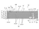
- FIG. 11 is a plan perspective view showing a wiring board according to Embodiment 3 of the present disclosure
- FIG. 11 is a vertical cross-sectional view of the wiring board according to Embodiment 3 cut along the signal line
- FIG. 11 is a plan perspective view of a main part of a wiring board according to Embodiment 3 as seen through from above
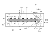
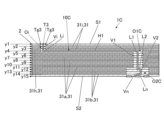
- FIG. 11 is a plan perspective view showing a wiring board according to Embodiment 4 of the present disclosure
- FIG. 11 is a vertical cross-sectional view of the wiring board according to Embodiment 4 cut along the signal line
- FIG. 11 is a plan perspective view of a main part of a wiring board according to Embodiment 4 as seen through from above
- FIG. 11 is a plan perspective view showing a wiring board according to Embodiment 3 of the present disclosure
- FIG. 11 is a vertical cross-sectional view of the wiring board according to Embodiment 3 cut along the signal line
- FIG. 11 is a plan perspective view of a main part of a
- FIG. 19 is a cross-sectional view showing the third layer in the main part of FIG. 18;
- FIG. 19 is a cross-sectional view showing a fourth layer in the main part of FIG. 18;
- FIG. 19 is a cross-sectional view showing fifth to tenth layers in the essential part of FIG. 18;
- FIG. 19 is a cross-sectional view showing the eleventh layer in the main part of FIG. 18;
- FIG. 19 is a cross-sectional view showing the twelfth layer in the main part of FIG. 18;
- FIG. 19 is a cross-sectional view showing the thirteenth layer in the main part of FIG. 18;
- FIG. 19 is a transverse cross-sectional view showing a fourteenth layer in the main part of FIG. 18;
- FIG. 19 is a transverse cross-sectional view showing a fourteenth layer in the main part of FIG. 18;
- FIG. 19 is a diagram showing the back surface of the main part of FIG. 18;
- FIG. 11 is a plan perspective view showing a wiring board according to Embodiment 5 of the present disclosure;
- FIG. 11 is a vertical cross-sectional view of the wiring board according to the fifth embodiment, cut along the signal line;
- FIG. 1A and 1B illustrate a wiring board according to Embodiment 1 of the present disclosure.
- FIG. 1A is a perspective plan view of the wiring board
- FIG. 1B is a longitudinal sectional view of the wiring board cut along a signal line. be.
- a wiring board 1 includes an insulating substrate 2 having a first surface S1 and a second surface S2 located opposite to the first surface S1, and first substrates located on the insulating substrate 2 and adjacent to each other.
- a line 10 and a second line 20 are provided.
- the insulating substrate 2 is a substrate having insulating properties such as ceramics or resin, and may have a laminated structure.
- the first line 10 and the second line 20 are a pair of differential lines through which differential signals are transmitted, and may be lines through which wideband signals are transmitted.
- the broadband may be a band from 1 GHz to 60 GHz.
- the wiring board 1 may further include a plurality of ground film conductors 31 and a plurality of ground via conductors 32 positioned on the insulating substrate 2 and surrounding the first line 10 and the second line 20 .
- the plurality of ground film conductors 31 and the plurality of ground via conductors 32 may have a configuration surrounding the first line 10 and the second line 20 together.
- the first line 10 includes, in order from the first surface S1 to the second surface S2 of the insulating substrate 2, the third electrode T3, the i-th via conductor Vi, the i-th line conductor Li, the first parallel line conductor H1, the 1 line conductor L1, first via conductor V1, second line conductor L2, second via conductor V2, nth line conductor Ln, nth via conductor Vn, and first electrode T1.
- the first electrode T ⁇ b>1 is located on the second surface S ⁇ b>2 of the insulating substrate 2 .
- the third electrode T3 is located on the first surface S1 of the insulating substrate 2 .
- the second line 20 is arranged in order from the first surface S1 to the second surface S2 of the insulating substrate 2, the fourth electrode T4, the i+1th via conductor Vi+1, the i+1th line conductor Li+1, the second parallel line conductor H2, the second parallel line conductor H2, and the second line conductor H2. It may have 3 line conductors L3, a third via conductor V3, a fourth line conductor L4, a fourth via conductor V4, an n+1th line conductor Ln+1, an n+1th via conductor Vn+1, and a second electrode T2.
- the second electrode T2 is located on the second surface S2 of the insulating substrate 2 .
- a fourth electrode T ⁇ b>4 is located on the first surface S ⁇ b>1 of the insulating substrate 2 .
- the first surface S1 side will be referred to as “upper”, and the second surface S2 side will be referred to as “lower”. Further, in the direction in which the parallel line conductors (H1, H2) extend, the direction in which the third electrode T3 and the fourth electrode T4 are positioned is “left”, and the direction in which the first electrode T1 and the second electrode T2 are positioned is “right”. method”.
- the wiring board 1 includes a plurality of electrodes (first electrode T1 to fourth electrode T4), line conductors (i-th line conductor Li to n+1-th line conductor Ln+1), or a plurality of ground film conductors 31. It may have layers (first layer y1 to fifteenth layer y15).
- the first layer y1 is the surface layer on the side of the first surface S1
- the fifteenth layer y15 is the surface layer on the side of the second surface S2.
- a plurality of layers are layers arranged in a vertical direction.
- the third electrode T3, the i-th line conductor Li, and the first parallel line conductor are arranged in this order from the left to the right.
- H1 the first line conductor L1, the second line conductor L2, the n-th line conductor Ln, and the first electrode T1 may be connected.
- the i-th line conductor Li, the first parallel line conductor H1, and the first line conductor L1 are located in the same layer. You may The first line conductor L1, the second line conductor L2, and the n-th line conductor Ln may be positioned in that order from top to bottom.
- a plurality of line conductors (the i-th line conductor Li, the first parallel line conductor H1, the first line conductor L1, the second line conductor L2, and the n-th line conductor Ln) included in the first line 10 have the same line width. may have.
- the i-th via conductor Vi may be located from the layer of the third electrode T3 to the layer of the i-th line conductor Li.
- the first via conductor V1 may be positioned from the layer of the first line conductor L1 to the layer of the second line conductor L2.
- the second via conductor V2 may be located from the layer of the second line conductor L2 to the layer of the n-th line conductor Ln.
- the n-th via conductor Vn may be located from the layer of the n-th line conductor Ln to the layer of the first electrode T1 (the layer of the second surface S2).
- the third electrode T3 may be located on the first layer y1.
- the i-th line conductor Li, the first parallel line conductor H1 and the first line conductor L1 may be located on the fourth layer y4.
- the second line conductor L2 may be located on the twelfth layer y12.
- the n-th line conductor Ln may be located on the fourteenth layer y14.
- the third electrode T3 may be connected to the top of the i-th via conductor Vi.
- the lower portion of the i-th via conductor Vi may be connected to the left portion of the i-th line conductor Li.
- the right portion of the i-th line conductor Li may be connected to the left portion of the first parallel line conductor H1.
- the right portion of the first parallel line conductor H1 may be connected to the left portion of the first line conductor L1.
- a right portion of the first line conductor L1 may be connected to an upper portion of the first via conductor V1.
- a lower portion of the first via conductor V1 may be connected to a left portion of the second line conductor L2.
- the right portion of the second line conductor L2 may be connected to the upper portion of the second via conductor V2.
- a lower portion of the second via conductor V2 may be connected to a left portion of the n-th line conductor Ln.
- the right portion of the nth line conductor Ln may be connected to the upper portion of the nth via conductor Vn.
- a lower portion of the n-th via conductor Vn may be connected to the first electrode T1.
- the connection positions of the upper and lower parts may be rephrased as upper and lower ends, respectively.
- the connection positions of the left part and the right part may be rephrased as the left end and the right end, respectively.
- the fourth electrode T4, the (i+1)-th line conductor Li+1, and the second parallel line conductor are arranged in this order from the left to the right when viewed through a plane (perpendicular to the first surface S1). H2, the third line conductor L3, the fourth line conductor L4, the (n+1)th line conductor Ln+1, and the second electrode T2 may be connected.
- the (i+1)th line conductor Li+1, the second parallel line conductor H2, and the third line conductor L3 are located in the same layer. You may The third line conductor L3, the fourth line conductor L4, and the (n+1)th line conductor Ln+1 may be positioned in that order from top to bottom.
- a plurality of line conductors (i+1th line conductor Li+1, second parallel line conductor H2, third line conductor L3, fourth line conductor L4, and n+1th line conductor Ln+1) included in the second line 20 have the same line width. may have.
- the plurality of line conductors included in the second line 20 may have the same line width as the plurality of line conductors included in the first line 10 .
- the i+1-th via conductor Vi+1 may be located from the layer of the fourth electrode T4 (the layer of the first surface S1) to the layer of the second parallel line conductor H2 and the third line conductor L3.
- the third via conductor V3 may be located from the layer of the third line conductor L3 to the layer of the fourth line conductor L4.
- the fourth via conductor V4 may be located from the layer of the fourth line conductor L4 to the layer of the (n+1)th line conductor Ln+1.
- the n+1-th via conductor Vn+1 may be located from the layer of the n+1-th line conductor Ln+1 to the layer of the second electrode T2 (the layer of the second surface S2).
- the fourth electrode T4 may be located on the first layer y1.
- the i+1th line conductor Li+1, the second parallel line conductor H2 and the third line conductor L3 may be located on the fourth layer y4.
- the fourth line conductor L4 may be located on the twelfth layer y12.
- the n+1th line conductor Ln+1 may be located on the fourteenth layer y14.
- the fourth electrode T4 may be connected to the top of the i+1th via conductor Vi+1.
- the lower portion of the i+1th via conductor Vi+1 may be connected to the left portion of the i+1th line conductor Li+1.
- the right portion of the i+1-th line conductor Li+1 may be connected to the left portion of the second parallel line conductor H2.
- the right portion of the second parallel line conductor H2 may be connected to the left portion of the third line conductor L3.
- the right portion of the third line conductor L3 may be connected to the upper portion of the third via conductor V3.
- a lower portion of the third via conductor V3 may be connected to a left portion of the fourth line conductor L4.
- a right portion of the fourth line conductor L4 may be connected to an upper portion of the fourth via conductor V4.
- a lower portion of the fourth via conductor V4 may be connected to a left portion of the (n+1)th line conductor Ln+1.
- the right portion of the n+1th line conductor Ln+1 may be connected to the upper portion of the n+1th via conductor Vn+1.
- a lower portion of the n+1th via conductor Vn+1 may be connected to the second electrode T2.
- the connection positions of the upper and lower parts may be rephrased as upper and lower ends, respectively.
- the connection positions of the left part and the right part may be rephrased as the left end and the right end, respectively.
- the i-th line conductor Li, the i+1-th line conductor Li+1, the first parallel line conductor H1, the second parallel line conductor H2, the first line conductor L1 and the third line conductor L3 are the same. It may be located in one layer.
- the second line conductor L2 and the fourth line conductor L4 may be located in the same layer.
- the n-th line conductor Ln and the n+1-th line conductor Ln+1 may be located in the same layer.
- the first parallel line conductor H1 and the second parallel line conductor H2 may be parallel.
- the first parallel line conductor H1 and the second parallel line conductor H2 may be straight or partially curved.
- the i-th via conductor Vi and the i+1-th via conductor Vi+1 may be positioned over the same layer.
- the first via conductor V1 and the third via conductor V3 may be positioned over the same layer.
- the second via conductor V2 and the fourth via conductor V4 may be positioned across the same layer.
- the n-th via conductor Vn and the n+1-th via conductor Vn+1 may be positioned across the same layer.
- the third electrode T3 and the fourth electrode T4 may be arranged in the front-rear direction (the direction perpendicular to the left-right direction and along the first surface S1 or the second surface S2).
- the first electrode T1 and the second electrode T2 may be arranged in the front-rear direction.
- the areas of the first electrode T1 and the second electrode T2 may be larger than the areas of the third electrode T3 and the fourth electrode T4.
- the distance between the center of the first electrode T1 and the center of the second electrode T2 may be longer than the distance between the center of the third electrode T3 and the center of the fourth electrode T4.
- the plurality of ground film conductors 31 may be positioned on all layers (second layer y2 to fourteenth layer y14) of the insulating substrate 2 except for the surface layer.
- the plurality of ground film conductors 31 includes one or more ground film conductors 31i having openings Oi surrounding the i-th via conductor Vi and the i+1-th via conductor Vi+1, a first parallel line conductor H1 and a second parallel line conductor H2. and a plurality of first ground film conductors 31a and a plurality of second ground film conductors 31b having a first opening O1 and a second opening O2, which will be described later.
- the opening Oh of the grounding film conductor 31h of the fourth layer y4 includes a belt-shaped portion along the first parallel line conductor H1 and the second parallel line conductor H2, a portion shaped like the opening Oh, and a portion shaped like the first opening O1. may have a congruent shape.
- the plurality of ground via conductors 32 may be positioned to surround at least the openings Oi, Oh, the first opening O1 and the second opening O2. Two adjacent ground via conductors 32 among the plurality of ground via conductors 32 may be spaced apart.
- the wiring board 1 may further have a third ground electrode Tg3 surrounding the third electrode T3 and a fourth ground electrode Tg4 surrounding the fourth electrode T4.
- the third ground electrode Tg3 and the fourth ground electrode Tg4 may be located on the first surface S1 of the insulating substrate 2 and connected to the ground film conductor 31 via the ground via conductor 32 .
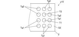
- the wiring board 1 may further have a plurality of first ground electrodes Tg1 and a plurality of second ground electrodes Tg2 surrounding the first electrodes T1 and the second electrodes T2.
- the plurality of first ground electrodes Tg1 and the plurality of second ground electrodes Tg2 may be positioned on the second surface S2 and spaced apart from each other around the first electrodes T1 and the second electrodes T2.
- each of the plurality of first ground electrodes Tg1 and the plurality of second ground electrodes Tg2 may be larger than the area of each of the third ground electrode Tg3 and the fourth ground electrode Tg4.
- the area surrounded by the first ground electrode Tg1 and the second ground electrode Tg2 may be larger than the area surrounded by the third ground electrode Tg3 and the fourth ground electrode Tg4.
- wideband differential signals can be transmitted between the first surface S1 and the second surface S2 of the insulating substrate 2 .
- FIG. 2 is a perspective plan view of a main part of the wiring board according to the first embodiment, seen from above.
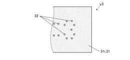
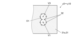
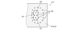
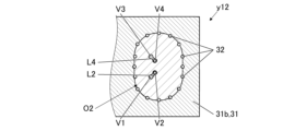
- 3A to 3C are cross-sectional views respectively showing the third layer, the fourth layer, and the fifth to tenth layers in the essential part of FIG. 4A to 4C are cross-sectional views respectively showing the 11th layer, the 12th layer, and the 13th layer in the essential part of FIG. 5A is a cross-sectional view showing the 14th layer in the main part of FIG. 2.
- FIG. 5B is a diagram showing the back surface of the main part of FIG. 2.
- FIG. 5B depicts the rear surface as seen through from above.
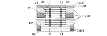
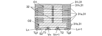
- FIG. 6A is a longitudinal cross-sectional view along line AA of FIG. 3B
- FIG. 6B is a longitudinal cross-sectional view along line BB of FIG. 3B
- FIG. 6C is a longitudinal cross-sectional view along line CC of FIG. 5A
- FIG. 5A is a vertical cross-sectional view taken along line DD of FIG.
- the first surface S1 (FIG. 1B) side will be described as “upper” and the second surface S2 side as “lower”. Further, in the direction in which the parallel line conductors (H1, H2) extend, the direction in which the third electrode T3 and the fourth electrode T4 are positioned is “left”, and the direction in which the first electrode T1 and the second electrode T2 are positioned is “right”. method”.
- the distance between the first line conductor L1 and the third line conductor L3 may gradually increase toward the right (Fig. 3B).
- the distance between the second line conductor L2 and the fourth line conductor L4 may gradually narrow toward the right (FIG. 4B).
- the gap between the second via conductor V2 and the fourth via conductor V4 is narrower than the gap between the first via conductor V1 and the third via conductor V3 (FIGS. 6B and 6C), and the first electrode T1 and the The inductance components of the first line 10 and the second line 20 can be increased in the vicinity of the second electrode T2.
- the large inductance component acts in the direction of canceling out the capacitive component of the first electrode T1 and the second electrode T2, so that good signal transmission characteristics can be obtained from low frequencies to high frequencies.
- first line conductor L1 and the third line conductor L3 may have a configuration in which the distance between them increases toward the first via conductor V1 and the third via conductor V3 in plan view. That is, in a plan view, the first line conductor L1 has a convex arc or circular arc on the third line conductor L3 side, a concave arc or circular arc on the third line conductor L3 side, a right angle, or at one or a plurality of positions at a certain angle. It may be a polygonal line shape, a stepped shape, or a shape that combines these shapes.
- the third line conductor L3 has a convex arc or circular arc on the first line conductor L1 side, a concave arc or circular arc on the first line conductor L1 side, a right angle, or at one or more locations at a certain angle. It may be a polygonal line shape that is bent at some points, a stepped shape, or a shape that combines these shapes.
- the second line conductor L2 and the fourth line conductor L4 may have a portion where the distance between them becomes smaller toward the second via conductor V2 and the fourth via conductor V4 in plan view. That is, in plan view, the second line conductor L2 has a convex arc or circular arc on the fourth line conductor L4 side, a concave arc or circular arc on the fourth line conductor L4 side, a right angle, or at one or a plurality of positions at a certain angle. It may be a polygonal line shape, a stepped shape, or a shape that combines these shapes.
- the fourth line conductor L4 has a convex arc or circular arc on the second line conductor L2 side, a concave arc or circular arc on the second line conductor L2 side, a right angle, or at one or more locations at a certain angle. It may be a polygonal line shape that is bent at some points, a stepped shape, or a shape that combines these shapes.
- the gap between the second via conductor V2 and the fourth via conductor V4 is narrower than the gap between the first via conductor V1 and the third via conductor V3, and the gap between the first electrode T1 and the second electrode T2 is narrower than the gap between the first via conductor V1 and the third via conductor V3.
- Inductance components of the first line 10 and the second line 20 can be increased in the vicinity. Then, the large inductance component acts in the direction of canceling out the capacitive component of the first electrode T1 and the second electrode T2, so that good signal transmission characteristics can be obtained from low frequencies to high frequencies.
- the first line conductor L1 and the third line conductor L3, and the second line conductor L2 and the fourth line conductor L4 may be separated vertically (FIGS. 6B and 6C). According to this configuration, the first via conductor V1 and the third via conductor V3 are located in a layer above the second line conductor L2 and the fourth line conductor L4, and the second via conductor V2 and the fourth via conductor V4 are located in the layer above the second line conductor L2 and the fourth line conductor L4. It will be located in the lower layer from the layer.
- the portion having a large inductance component approaches the first electrode T1 and the second electrode T2, and the capacitive component of the first electrode T1 and the second electrode T2 is reduced. It is easy to get the effect of canceling. Therefore, better signal transmission characteristics can be obtained from low frequencies to high frequencies.
- the first line conductor L1 and the third line conductor L3 may be positioned closer to the first surface S1 than the center of the insulating substrate 2 in the thickness direction.
- the second line conductor L2 and the fourth line conductor L4 may be positioned closer to the second surface S2 than the center of the insulating substrate 2 in the thickness direction.
- the first via conductor V1 and the third via conductor V3 with a wide interval are positioned in a long range including the center in the vertical direction of the insulating substrate 2, while the second via conductor V2 and the fourth via conductor with a narrow interval are located.
- the conductor V4 will be located near the first electrode T1 and the second electrode T2.
- the vertical lengths of the narrowly spaced second and fourth via conductors V2 and V4 are shorter than the vertical lengths of the widely spaced first and third via conductors V1 and V3. Therefore, the large inductance components associated with the second via conductor V2 and the fourth via conductor V4 act to cancel the capacitance components associated with the first electrode T1 and the second electrode T2.
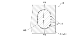
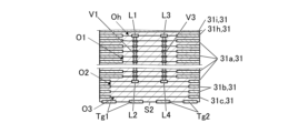
- the plurality of grounding film conductors 31 includes a first grounding film conductor 31a having a first opening O1 (FIGS. 4A and 1B) and a second grounding film conductor 31a having a second opening O2 (FIGS. 4B-5A and 1B). 31b.
- a first via conductor V1 and a third via conductor V3 may be positioned within the first opening O1
- a third via conductor V3 and a fourth via conductor V4 may be positioned within the second opening O2.
- the first opening O1 may be smaller than the second opening O2.
- the second via conductor V2 and the fourth via conductor V4 having a large inductance component are located inside the large second opening O2, the second via conductor V2 and the fourth via conductor V4 are separated from the ground potential. can be spaced further apart. Therefore, the capacitive components of the second via conductor V2 and the fourth via conductor V4 having large inductance components are reduced, and the effect of canceling the capacitive components of the first electrode T1 and the second electrode T2 is increased. Therefore, the impedance can be better matched, and better signal transmission characteristics can be obtained from low frequencies to high frequencies.
- the first electrode T1, the second electrode T2, the plurality of first ground electrodes Tg1, and the plurality of second ground electrodes Tg2 may have a larger area than the third electrode T3 and the fourth electrode T4.
- the capacitance component increases in the vicinity of the first electrode T1 and the second electrode T2. can cancel out the increase in Therefore, according to the wiring board 1 of Embodiment 1, the first electrode T1, the second electrode T2, the plurality of first ground electrodes Tg1, and the plurality of second ground electrodes Tg2 are enlarged without impairing the signal transmission characteristics. and the ease of mounting on the second surface S2 side can be improved.
- the center (corresponding to the central portion) P1 of the first opening O1 is located between the center (corresponding to the central portion) P2 of the second opening O2 and the first parallel line conductor H1 and the second parallel line conductor H2. may be located (Fig. 2).
- the first via conductor V1 and the third via conductor V3 are arranged near the center of the first opening O1
- the second via conductor V2 and the fourth via conductor V4 are arranged near the center of the second opening O2.
- the second opening O2 of the ground film conductor 31 of the fourteenth layer y14 may be called a third opening O3 (Fig. 5A). At least part of the n-th via conductor Vn connected to the first electrode T1 and the n+1-th via conductor Vn+1 connected to the second electrode T2 are located in the third opening O3.
- the third opening O3 has the same size and position as the second opening O2 positioned above the fourteenth layer y14 in planar perspective. However, the second opening O2 and the third opening O3 may differ in size and position when viewed from above.
- the third opening O3 may be larger than the first opening O1.
- the third opening O3 may be smaller, larger, or the same size as the second opening O2.
- the first via conductor V1 and the third via conductor V3 may be positioned at the center of the first opening O1 in the horizontal direction (corresponding to the X direction according to the present disclosure).
- the n-th via conductor Vn and the n+1-th via conductor Vn+1 may be positioned at the center of the third opening O3 in the horizontal direction.
- the ground conductor is positioned symmetrically with respect to the conductor through which the signal is transmitted, so that better impedance matching can be achieved.
- the via conductors (the i-th via conductor Vi, the first via conductor V1, the second via conductor V2, the n-th via conductor Vn) of the first line 10, the first via counted from the one closest to the first electrode T1
- the conductor is the nth via conductor Vn
- the second via conductor is the second via conductor V2 (corresponding to the n+2th via conductor according to the present disclosure).
- one The second via conductor is the n+1th via conductor Vn+1
- the second via conductor is the fourth via conductor V4 (corresponding to the n+3th via conductor according to the present disclosure).
- the second distance between the second via conductor V2 and the fourth via conductor V4 from the first electrode T1 and the second electrode T2 is the first distance from the first electrode T1 and the second electrode T2. may be narrower than the interval between the n-th via conductor Vn and the n+1-th via conductor Vn+1.
- the second via conductor V2 and the fourth via conductor V4 (corresponding to the (n+2)th via conductor and the (n+3)th via conductor according to the present disclosure) which are closely spaced are arranged near the first electrode T1 and the second electrode T2.
- the large inductance components associated with the second via conductor V2 and the fourth via conductor V4 act to cancel the capacitance components associated with the first electrode T1 and the second electrode T2.
- the n-th via conductor Vn can be brought closer to the center of the first electrode T1, and the n+1-th via conductor Vn+1 can be brought closer to the center of the second electrode T2. be able to. Therefore, good signal transmission characteristics can be obtained.
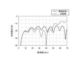
- FIGS. 7A and 7B are graphs showing the reflection loss and insertion loss of the wiring board 1 according to the first embodiment and the comparative example, respectively.
- Graphs of FIGS. 7A and 7B show simulation results for the wiring board 1 of the first embodiment and the wiring board of the comparative example.
- the wiring board of the comparative example has a configuration in which the following components 1 to 4 are changed from the configuration of the first embodiment.
- Component 1 second line conductor L2, second via conductor V2, nth line conductor Ln, nth via conductor Vn, fourth line conductor L4, fourth via conductor V4, n+1th line conductor Ln+1, n+1th via conductor Remove Vn+1.
- Component 2 The first via conductor V1 of Embodiment 1 is positioned in the center of the first electrode T1, and the first via conductor V1 extends to the first electrode T1 when seen from above.
- Component 3 The second via conductor V2 is positioned in the center of the second electrode T2 and extends to the second electrode T2 in plan perspective view.
- Component 4 The center of the first opening O1, the center of the second opening O2, and the centers of the first via conductor V1 and the center of the second via conductor V2 overlap with each other in plan view.
- FIGS. 7A and 7B show that, compared to the comparative example, the wiring board 1 of Embodiment 1 has a low reflection loss even in a high frequency band, and the high insertion loss of Embodiment 1 also has a low frequency band. It shows that good signal transmission characteristics can be obtained from low frequencies to high frequencies.
- the wiring board 1 of Embodiment 1 has been described above with reference to the drawings.
- the wiring board 1 of Embodiment 1 is not limited to the illustrated configuration.
- the interval between the second via conductor V2 and the fourth via conductor V4 may be larger than the interval between the first parallel line conductor H1 and the second parallel line conductor H2, They may be the same, or they may be smaller.
- the distance between the first via conductor V1 and the third via conductor V3 may be greater than or equal to the distance between the nth via conductor Vn and the n+1th via conductor Vn+1. , can be smaller.
- the second line conductor L2 and the fourth line conductor L4 are located on the 12th layer y12, and the n-th line conductor Ln and the n+1-th line conductor Ln+1 are located on the 14th layer y14. Indicated. However, the second line conductor L2 and the fourth line conductor L4 may be located on any of the eighth layer y8 to the thirteenth layer y13, and the nth line conductor Ln and the n+1th line conductor Ln+1 may be located on the second layer y8 to the thirteenth layer y13. It may be located in any one of the ninth layer y9 to the thirteenth layer y13 below the line conductor L2 and the fourth line conductor L4.
- the first line 10 and the second line 20 are symmetrical with respect to a plane extending in the upper limit direction and the left-right direction between the first parallel line conductor H1 and the second parallel line conductor H2. Although an example is shown, it may have a non-plane symmetrical portion. Further, instead of the stripline structure described in the first embodiment, the i-th line conductor Li and the first parallel line conductor H1 are connected from the third electrode T3 on the first surface S1 except for the i-th via conductor Vi.
- a so-called microstrip line structure may be employed in which the i+1-th line conductor Li+1 and the second parallel line conductor H2 are connected from the fourth electrode T4 on the first surface S1 except for the i+1-th via conductor Vi+1. This also applies to the second embodiment, which will be described later.
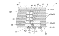
- FIG. 8A is a perspective plan view showing a main part of a wiring board according to Embodiment 2 of the present disclosure
- 8B is a vertical cross-sectional view of a main part of the wiring board according to the second embodiment of the present disclosure, cut along the signal line
- FIG. 9A to 9C are cross-sectional views respectively showing the third layer, fourth layer, and fifth to ninth layers in the essential part of FIG. 8A
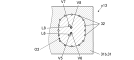
- 10A to 10C are cross-sectional views respectively showing the 10th, 11th, and 12th layers in the essential part of FIG. 8A.
- 11A and 11B are cross-sectional views respectively showing the 13th layer and the 14th layer in the main part of FIG. 8A.
- FIG. 11C is a diagram showing the back surface of the main part of FIG. 8A.
- FIG. 11C depicts the back surface seen through from above.
- FIG. 12A is a vertical cross-sectional view taken along line AA of FIG. 9B.
- FIG. 12B is a vertical cross-sectional view taken along line BB of FIG. 9B.
- FIG. 12C is a vertical cross-sectional view taken along line CC of FIG. 10C.
- FIG. 13A is a vertical cross-sectional view taken along line DD of FIG. 10C.
- FIG. 13B is a vertical cross-sectional view taken along line EE of FIG. 11B.
- FIG. 13C is a vertical cross-sectional view taken along line FF of FIG. 11B.
- the wiring board 1A of the second embodiment includes an insulating substrate 2, a first line 10A and a second line 20A located on the insulating substrate 2 and adjacent to each other, and a first line 10A and a second line 20A located on the insulating substrate 2.
- a plurality of ground film conductors 31 and a plurality of ground via conductors 32 are provided surrounding 20A.
- the first line 10A is the same as the first line 10 of the first embodiment from the third electrode T3 to the second line conductor L2 and from the first electrode T1 to the nth line conductor Ln.
- the second line 20A is the same as the second line 20 of the first embodiment from the fourth electrode T4 to the fourth line conductor L4 and from the second electrode T2 to the (n+1)th line conductor Ln+1.
- the same components as in the first embodiment are given the same reference numerals, and detailed descriptions thereof are omitted.
- the first line 10A includes a second via conductor V2, a fifth line conductor L5, a fifth via conductor V5, a sixth line conductor L6, and a sixth via conductor between the second line conductor L2 and the nth line conductor Ln.
- V6 may be included.
- the right portion of the second via conductor L2 is connected to the upper portion of the second via conductor V2
- the lower portion of the second via conductor V2 is connected to the left portion of the fifth line conductor L5
- the right portion of the fifth line conductor L5 is connected to the upper portion of the fifth line conductor L5. It may be connected to the top of the 5-via conductor V5.
- the left portion of the sixth line conductor L6 is connected to the bottom portion of the fifth via conductor V5
- the right portion of the sixth line conductor L6 is connected to the top portion of the sixth via conductor V6
- the bottom portion of the sixth via conductor V6 is connected to It may be connected to the left portion of the n-th line conductor Ln.
- the right part, left part, upper part and lower part may be rephrased as right end, left end, upper end and lower end, respectively.
- the second line 20A includes a fourth via conductor V4, a seventh line conductor L7, a seventh via conductor V7, an eighth line conductor L8, and an eighth via conductor between the fourth line conductor L4 and the (n+1)th line conductor Ln+1. V8 may be included.
- the right portion of the fourth line conductor L4 is connected to the top of the fourth via conductor V4
- the bottom of the fourth via conductor V4 is connected to the left portion of the seventh line conductor L7
- the right portion of the seventh line conductor L7 is connected to the top of the seventh line conductor L7. 7 may be connected to the top of the via conductor V7.
- the left portion of the eighth line conductor L8 is connected to the bottom portion of the seventh via conductor V7
- the right portion of the eighth line conductor L8 is connected to the top portion of the eighth via conductor V8
- the bottom portion of the eighth via conductor V8 is connected to It may be connected to the left portion of the n+1-th line conductor Ln+1.
- the right part, left part, upper part and lower part may be rephrased as right end, left end, upper end and lower end, respectively.
- the second line conductor L2 and the fourth line conductor L4 may be located on the eleventh layer y11 and the spacing may gradually narrow toward the right.
- the fifth line conductor L5 and the seventh line conductor L7 may be located on the twelfth layer y12, and the spacing may gradually widen toward the right.
- the sixth line conductor L6 and the eighth line conductor L8 (FIG. 11A) may be located on the thirteenth layer y13 and the spacing may gradually narrow toward the right.
- the distance between the second via conductor V2 and the fourth via conductor V4 is narrower than the distance between the first via conductor V1 and the third via conductor V3, and the distance between the second via conductor V2 and the fourth via conductor V4 is reduced.
- the distance between the sixth via conductor V6 and the eighth via conductor V8 becomes narrower than the distance between the fifth via conductor V5 and the seventh via conductor V7
- the distance between the sixth via conductor V6 and the eighth via conductor V8 becomes narrower than the distance between the fifth via conductor V5 and the seventh via conductor V7.
- the large inductance component acts to cancel out the capacitive components of the first electrode T1 and the second electrode T2, and good signal transmission characteristics can be obtained from low frequencies to high frequencies.
- the wiring substrate 1A has a plurality of locations (the interval between the second via conductor V2 and the fourth via conductor V4, the interval between the second via conductor V2 and the fourth via conductor V4, the interval between the sixth via conductor V6 and the eighth via conductor V8), and the interval between the via conductors can be narrowed. ). Therefore, the degree of freedom in adjusting the impedance is improved when designing the wiring board 1A. Therefore, impedance matching is facilitated, and favorable signal transmission characteristics are easily obtained.
- the second line conductor L2 and the fourth line conductor L4 may have a portion where the distance between them decreases toward the second via conductor V2 and the fourth via conductor V4 in plan view. That is, in plan view, the second line conductor L2 has a convex arc or circular arc on the fourth line conductor L4 side, a concave arc or circular arc on the fourth line conductor L4 side, a right angle, or at one or a plurality of positions at a certain angle. It may be a polygonal line shape, a stepped shape, or a shape that combines these shapes.
- the fourth line conductor L4 has a convex arc or circular arc on the second line conductor L2 side, a concave arc or circular arc on the second line conductor L2 side, a right angle, or at one or more locations at a certain angle. It may be a polygonal line shape that is bent at some points, a stepped shape, or a shape that combines these shapes.
- the fifth line conductor L5 and the seventh line conductor L7 may have a portion where the distance between them increases toward the fifth via conductor V5 and the seventh via conductor V7 in plan view. That is, in a plan view, the fifth line conductor L5 has a convex arc or circular arc on the seventh line conductor L7 side, a concave arc or circular arc on the seventh line conductor L7 side, a right angle, or at one or more places at a certain angle. It may be a polygonal line shape, a stepped shape, or a shape that combines these shapes.
- the seventh line conductor L7 has a convex arc or circular arc on the fifth line conductor L5 side, a concave arc or circular arc on the fifth line conductor L5 side, a right angle, or at one or more locations at a certain angle. It may be a polygonal line shape that is bent at some points, a stepped shape, or a shape that combines these shapes.
- the sixth line conductor L6 and the eighth line conductor L8 may have a portion where the distance between them becomes smaller toward the sixth via conductor V6 and the eighth via conductor V8 in plan view. That is, in a plan view, the sixth line conductor L6 has a convex arc or circular arc on the eighth line conductor L8 side, a concave arc or circular arc on the eighth line conductor L8 side, a right angle, or at one or more places at a certain angle. It may be a polygonal line shape, a stepped shape, or a shape that combines these shapes.
- the eighth line conductor L8 has a convex arc or circular arc on the sixth line conductor L6 side, a concave arc or circular arc on the sixth line conductor L6 side, a right angle, or at one or more locations at a certain angle. It may be a polygonal line shape that is bent at some points, a stepped shape, or a shape that combines these shapes.
- the distance between the second via conductor V2 and the fourth via conductor V4 is narrower than the distance between the first via conductor V1 and the third via conductor V3.
- the inductance component can be increased.
- the distance between the sixth via conductor V6 and the eighth via conductor V8 becomes narrower than the distance between the fifth via conductor V5 and the seventh via conductor V7, and the distance between the sixth via conductor V6 and the eighth via conductor V8 becomes narrower than the distance between the fifth via conductor V5 and the seventh via conductor V7. can increase the inductance component.
- the large inductance component acts to cancel out the capacitive components of the first electrode T1 and the second electrode T2, and good signal transmission characteristics can be obtained from low frequencies to high frequencies. Furthermore, the degree of freedom in adjusting the impedance when designing the wiring board 1A is improved.
- the first electrode The first via conductor counted from the side closer to T1 is the nth via conductor Vn, and the second via conductor is the sixth via conductor V6 (corresponding to the n+2th via conductor according to the present disclosure).
- the via conductors i+1th via conductor Vi+1, third via conductor V3, fourth via conductor V4, seventh via conductor V7, eighth via conductor V8, n+1th via conductor Vn+1
- the first via conductor counted from the side closer to the second electrode T2 is the n+1th via conductor Vn+1
- the second via conductor is the eighth via conductor V8 (corresponding to the n+3th via conductor according to the present disclosure).
- the distance between the second sixth via conductor V6 and the eighth via conductor V8 from the first electrode T1 and the second electrode T2 is the first distance from the first electrode T1 and the second electrode T2. may be narrower than the interval between the n-th via conductor Vn and the n+1-th via conductor Vn+1.
- the sixth via conductor V6 and the eighth via conductor V8 (corresponding to the n+2-th via conductor and the n+3-th via conductor according to the present disclosure) with narrow spacing are arranged near the first electrode T1 and the second electrode T2. can be placed in Therefore, the large inductance components associated with the sixth via conductor V6 and the eighth via conductor V8 act to cancel the capacitance components associated with the first electrode T1 and the second electrode T2.
- the large inductance components associated with the sixth via conductor V6 and the eighth via conductor V8 can reduce the impediment of impedance matching at sites away from the first electrode T1 and the second electrode T2. Therefore, better signal transmission characteristics can be obtained from low frequencies to high frequencies.
- the plurality of ground film conductors 31 are located on the second layer y2 to the fourteenth layer y14 of the insulating substrate 2, as in the first embodiment. Furthermore, the openings Oi and Oh included in the plurality of ground film conductors 31 are the same as in the first embodiment. Furthermore, the plurality of grounding film conductors 31 according to the second embodiment includes first grounding film conductors 31a having first openings O1 (FIGS. 8B, 9C, and 10A) and second openings O2 (FIGS. 8B, 10B- 11A) and a third grounding film conductor 31c having a third opening O3 (FIGS. 8B and 11B).
- the first opening O1 may be located in a layer (fifth layer y5 to tenth layer y10) through which the first via conductor V1 and the third via conductor V3 are located.
- the second opening O2 is a layer (the eleventh It may be located in the layer y11 to the thirteenth layer y13).
- the third opening O3 may be located in a layer (14th layer y14) one layer above the layer in which the electrodes (T1, T2, Tg1, Tg2) are located.
- the first opening O1 may have a size that achieves impedance matching between the first via conductor V1 and the third via conductor V3.
- the third openings O3 are formed so that the plurality of first ground electrodes Tg1 and the plurality of second ground electrodes Tg2 and the third ground film conductor 31c can be connected via the plurality of ground via conductors 32. It may have a size corresponding to the arrangement of the ground electrode Tg1 and the plurality of second ground electrodes Tg2.
- the second opening O2 may be larger than the first opening O1.
- the second opening O2 may be larger than the third opening O3, may have the same size as the third opening O3, or may be smaller than the third opening O3.
- the second opening O2 is larger than the first opening O1
- the second via conductor V2 and the fourth via conductor V4, and the sixth via conductor V6 and the eighth via conductor V8, which have large inductance components, are separated from the ground potential. can be spaced further apart. Therefore, the capacitive components of the second via conductor V2 and the fourth via conductor V4 as well as the sixth via conductor V6 and the eighth via conductor V8 are reduced, and the capacitive components of the first electrode T1 and the second electrode T2 are canceled. action becomes greater.
- the center (corresponding to the central portion) P1 of the first opening O1 is aligned with the center (corresponding to the central portion) P2 of the second opening O2, the first parallel line conductor H1 and the second parallel line conductor H2. may be located between
- the first via conductor V1 and the third via conductor V3 are arranged near the center of the first opening O1
- the second via conductor V2 and the fourth via conductor V4 are arranged near the center of the second opening O2.
- the center P2 of the second opening O2 may be located between the center P3 of the third opening O3 and the center P1 of the first opening O1.
- the second via conductor V2, the fourth via conductor V4 to the eighth via conductor V8 are arranged near the center of the second opening O2
- the nth via conductor Vn and the n+1th via conductor Vn+1 are arranged in the third opening O2. It can be arranged near the center of the opening O3. Therefore, impedance matching at the second opening O2 and impedance matching at the third opening O3 can be achieved, and better signal transmission characteristics can be obtained.
- the first via conductor V1 and the third via conductor V3 may be positioned at the center of the first opening O1 in the horizontal direction (corresponding to the X direction according to the present disclosure).
- the n-th via conductor Vn and the n+1-th via conductor Vn+1 may be positioned at the center of the third opening O3 in the horizontal direction.
- the ground conductor is positioned symmetrically with respect to the conductor through which the signal is transmitted, so that better impedance matching can be achieved.
- the wiring board 1A of the second embodiment has been described above with reference to the drawings.
- the wiring board 1A of the second embodiment is not limited to the illustrated configuration.
- the distance between the first parallel line conductor H1 and the second parallel line conductor H2, the distance between the second via conductor V2 and the fourth via conductor V4, the distance between the sixth via conductor V6 and the eighth via conductor V8 may be all the same, all may be different, or some may be the same and the rest may be different.
- the order of magnitude of the three intervals may be any order.
- the intervals may be all the same, all may be different, or some may be the same and the rest may be different.
- the order of magnitude of the three intervals may be any order.
- FIG. 3 is a perspective plan view showing a wiring board according to Embodiment 3 of the present disclosure
- FIG. 15B is a vertical cross-sectional view of the wiring board according to Embodiment 3 cut along the signal line.
- FIG. FIG. 16 is a perspective plan view of a main part of the wiring board according to the third embodiment, seen from above.
- the wiring board 1B of Embodiment 3 is an example in which the center (corresponding to the central portion) P1 of the first opening O1B is positioned to the right of the center (corresponding to the central portion) P2 of the second opening O2B in plan view. .
- the relative arrangement of the first opening O1B and the second opening O2B, the path of the first line 10B, and the path of the second line 20B are mainly the same as in the first or second embodiment.
- other elements may be similar to Embodiment 1 or Embodiment 2.
- the center P1 of the first opening O1B may be located to the right of the center P2 of the second opening O1B.
- the center P2 of the second opening O2B may be located between the center P1 of the first opening O1B and the point P11 on the parallel line side.
- the point P11 on the parallel line side is the center P11 of the intersection of the edge of the second opening O2B and the first parallel line conductor H1 and the intersection of the edge of the second opening O2B and the second parallel line conductor H2.
- the first parallel line conductor H1 and the second parallel line conductor H2 may be parallel.
- the first parallel line conductor H1 and the second parallel line conductor H2 may be straight or partially curved. Even if the above arrangement is adopted, good signal transmission characteristics can be obtained from low frequencies to high frequencies.
- the first via conductor V1 and the third via conductor V3 are positioned to the right of the second via conductor V2 and the fourth via V4 in plan view.
- the interval between the first via conductor V1 and the third via conductor V3 is wider than the interval between the second via conductor V2 and the fourth via conductor V4.
- the n-th via conductor Vn and the n+1-th via conductor Vn+1 are positioned to the left of the second via conductor V2 and the fourth via conductor V4.
- the interval between the nth via conductor Vn and the n+1th via conductor Vn+1 is wider than the interval between the second via conductor V2 and the fourth via conductor V4.
- the second line conductor L2 and the fourth line conductor L4 are arranged between the lower end of the first via conductor V1 and the upper end of the second via conductor V2, and between the lower end of the third via conductor V3 and the fourth via conductor V4. each extending between the upper ends. That is, the second line conductor L2 and the fourth line conductor L4 extend so that the distance therebetween narrows toward the left. Further, the n-th line conductor Ln and the n+1-th line conductor Ln+1 are located between the lower end of the third via conductor V3 and the upper end of the n-th via conductor Vn, and between the lower end of the fourth via conductor V4 and the upper end of the n+1-th conductor Vn+1. and extend respectively between That is, the n-th line conductor Ln and the n+1-th line conductor Ln+1 extend so that the distance increases toward the left.
- first line conductor L1 may overlap part or all of the second line conductor L2, and the third line conductor L3 may overlap part or all of the fourth line conductor L4.
- via conductors, line conductors, and stepped portions are provided on the first line 10B and the second line 20B.
- each stepped portion is included is shown, four or more steps may be included in each step.
- a configuration in which the first via conductor V1 and the third via conductor V3 are positioned to the right of the nth via conductor Vn and the n+1th via conductor Vn+1 in plan view can be employed. Also in this configuration, good signal transmission characteristics can be obtained from low frequencies to high frequencies.
- FIG. 4 is a plan perspective view showing a wiring board according to Embodiment 4 of the present disclosure
- FIG. 17B is a vertical cross-sectional view of the wiring board according to Embodiment 4 cut along the signal line.
- FIG. FIG. 18 is a perspective plan view of a main part of the wiring board according to the fourth embodiment, seen from above.
- 19A to 19H show the 3rd layer, 4th layer, 5th layer to 10th layer, 11th layer, 12th layer, 13th layer, 14th layer, and the back surface of the main part of FIG. It is a diagram.
- the wiring board 1C of Embodiment 4 is an example in which the center (corresponding to the central portion) P1 of the first opening O1C coincides with the center (corresponding to the central portion) P2 of the second opening O2C in plan view.
- Matching is not limited to strict matching, but includes the case where the positional difference is equal to or less than the minimum value of the diameter of the via conductor.
- Embodiment 4 is different from Embodiments 1, 2, and 3 mainly in the relative arrangement of the first opening O1C and the second opening O2C, the path of the first line 10C, and the path of the second line 20C. Differently, other elements may be the same as those of the first, second, and third embodiments.
- the center P1 of the first opening O1C may coincide with the center P2 of the second opening O1C. Even if this arrangement is adopted, good signal transmission characteristics can be obtained from low frequencies to high frequencies.
- the second via conductors V2 and the fourth via conductors V4 are positioned laterally apart from the first via conductors V1 and the third via conductors V3 in plan view.
- the interval between the first via conductor V1 and the third via conductor V3 is wider than the interval between the second via conductor V2 and the fourth via conductor V4.
- the n-th via conductor Vn and the n+1-th via conductor Vn+1 are positioned laterally apart from the second via conductor V2 and the fourth via conductor V4, and the first via conductor V1 and the third via conductor V3 are positioned so as to overlap each other.
- the interval between the nth via conductor Vn and the n+1th via conductor Vn+1 is wider than the interval between the second via conductor V2 and the fourth via conductor V4.
- the second line conductor L2 and the fourth line conductor L4 are arranged between the lower end of the first via conductor V1 and the upper end of the second via conductor V2, and between the lower end of the third via conductor V3 and the fourth via conductor V4. each extending between the upper ends.
- the second line conductor L2 and the fourth line conductor L4 extend so that the closer they are to the second via conductor V2 and the fourth via conductor V4, the closer the distance between them becomes.
- the n-th line conductor Ln and the n+1-th line conductor Ln+1 are located between the bottom end of the second via conductor V2 and the top end of the n-th via conductor Vn, and between the bottom end of the fourth via conductor V4 and the top end of the n+1-th conductor Vn+1. and extend respectively between That is, the n-th line conductor Ln and the n+1-th line conductor Ln+1 extend so that the distance between them increases as they are closer to the n-th via conductor Vn and the n+1-th via conductor Vn+1.
- the second line conductor L2 may overlap part or all of the n-th line conductor Ln
- the fourth line conductor L4 may overlap part or all of the n+1-th line conductor Ln+1.
- via conductors, line conductors, and stepped portions are provided on the first line 10C and the second line 20C.
- each step is included is shown, four or more of the stepped portions are included, and in a plan view, the n-th via conductor Vn and the n+1-th via conductor Vn+1, the first via conductor V1 and the second via conductor V2. may be adopted. Also in this configuration, good signal transmission characteristics can be obtained from low frequencies to high frequencies.
- FIG. 5 is a perspective plan view showing a wiring board according to Embodiment 5 of the present disclosure
- FIG. 20B is a longitudinal sectional view of the wiring board according to the fifth embodiment cut along the signal line.
- FIG. 5 is a perspective plan view showing a wiring board according to Embodiment 5 of the present disclosure
- FIG. 20B is a longitudinal sectional view of the wiring board according to the fifth embodiment cut along the signal line.
- the center (corresponding to the central portion) P1 of the first opening O1D coincides with the center (corresponding to the central portion) P2 of the second opening O2D in plan view.
- the wiring board 1D of the fifth embodiment four via conductors, line conductors, and stepped portions (see FIG. 20B) connected to the via conductors are provided for the first line 10D and the second line 20D in the first opening O1D. Examples include each.
- Embodiment 5 is different from Embodiments 1, 2, and 3 mainly in the relative arrangement of the first opening O1D and the second opening O2D, the path of the first line 10D, and the path of the second line 20D. Differently, other elements may be the same as those of the first, second, and third embodiments.
- the center P1 of the first opening O1D may coincide with the center P2 of the second opening O1D. Even if this arrangement is adopted, good signal transmission characteristics can be obtained from low frequencies to high frequencies.
- the first via conductor V1, the fifth via conductor V5, and the n-th via conductor Vn may overlap in plan view.
- the third via conductor V3, the seventh via conductor V7, and the (n+1)th via conductor Vn+1 may overlap.
- the second via conductor V2 and the fourth via conductor V4 may be positioned laterally apart from the first via conductor V1 and the third via conductor V3. The interval between the second via conductor V2 and the fourth via conductor V4 may be narrower than the interval between the first via conductor V1 and the third via conductor V3.
- the sixth via conductor V6 and the eighth via conductor V8 may be positioned laterally apart from the first via conductor V1 and the third via conductor V3.
- the sixth via conductor V6 and the eighth via conductor V8 may be located on the opposite side in the horizontal direction from the second via conductor V2 and the fourth via conductor V4.
- the interval between the sixth via conductor V6 and the eighth via conductor V8 may be narrower than the interval between the first via conductor V1 and the third via conductor V3.
- the second line conductor L2 and the fourth line conductor L4 are arranged between the lower end of the first via conductor V1 and the upper end of the second via conductor V2, and between the lower end of the third via conductor V3 and the fourth via conductor V4. each extending between the upper ends.
- the second line conductor L2 and the fourth line conductor L4 extend so that the closer they are to the second via conductor V2 and the fourth via conductor V4, the closer the distance between them becomes.
- the fifth line conductor L5 and the seventh line conductor L7 are arranged between the lower end of the second via conductor V2 and the upper end of the fifth via conductor V5 and between the lower end of the fourth via conductor V4 and the seventh via conductor V7. each extending between the upper ends. That is, the fifth line conductor L5 and the seventh line conductor L7 extend so that the distance between the fifth via conductor V5 and the seventh via conductor V7 increases.
- the second line conductor L2 may overlap part or all of the fifth line conductor L5, and the fourth line conductor L4 may overlap part or all of the seventh line conductor L7.
- the sixth line conductor L6 and the eighth line conductor L8 are arranged between the lower end of the fifth via conductor V5 and the upper end of the sixth via conductor V6 and between the lower end of the seventh via conductor V7 and the eighth via conductor V8. each extending between the upper ends.
- the sixth line conductor L6 and the eighth line conductor L8 extend so that the distance between the sixth via conductor V6 and the eighth via conductor V8 becomes narrower.
- the n-th line conductor Ln and the n+1-th line conductor Ln+1 are arranged between the lower end of the sixth via conductor V6 and the upper end of the n-th via conductor Vn, and between the lower end of the eighth via-conductor V8 and the n+1-th via conductor Vn+1. each extending between the upper ends. That is, the n-th line conductor Ln and the n+1-th line conductor Ln+1 extend so that the distance between them increases as they are closer to the n-th via conductor Vn and the n+1-th via conductor Vn+1.
- the sixth line conductor L6 may overlap part or all of the nth line conductor Ln
- the eighth line conductor L8 may overlap part or all of the n+1th line conductor Ln+1.
- FIG. 14 is a diagram illustrating an electronic device and an electronic module according to an embodiment of the present disclosure.
- An electronic device 80 according to this embodiment includes a wiring board 1 and an electronic element 82 mounted on the wiring board 1 .
- Wiring board 1 may be replaced by wiring boards 1A to 1D.
- the electronic element 82 is an element to which a high-frequency signal is input, output, or input and output, and is electrically connected to the third electrode T3 and the fourth electrode T4 of the wiring board 1 .
- Electronic device 82 may be a semiconductor device.
- the high frequency signal may be a differential signal.
- the electronic module 100 includes a module board 110 and an electronic device 80 mounted on the module board 110 .
- the module substrate 110 may be mounted with other electronic devices, electronic elements, electric elements, and the like.
- the module substrate 110 has a plurality of electrodes 111 on the mounting portion of the electronic device 80.
- the electrodes Tg2 may be connected via the conductive bonding material 113 respectively.
- the electronic device 80 and the electronic module 100 according to the present embodiment can obtain good characteristics from low frequencies to high frequencies due to the wiring board 1 (or the wiring boards 1A to 1D) having a wide band.
- the present disclosure can be used for wiring boards, electronic devices, and electronic modules.
Landscapes
- Engineering & Computer Science (AREA)
- Microelectronics & Electronic Packaging (AREA)
- Manufacturing & Machinery (AREA)
- Chemical & Material Sciences (AREA)
- Ceramic Engineering (AREA)
- Inorganic Chemistry (AREA)
- Structure Of Printed Boards (AREA)
- Production Of Multi-Layered Print Wiring Board (AREA)
Priority Applications (3)
| Application Number | Priority Date | Filing Date | Title |
|---|---|---|---|
| JP2023564995A JP7770421B2 (ja) | 2021-11-30 | 2022-11-29 | 配線基板、電子装置及び電子モジュール |
| KR1020247017796A KR20240093974A (ko) | 2021-11-30 | 2022-11-29 | 배선 기판, 전자 장치 및 전자 모듈 |
| CN202280078518.XA CN118303139A (zh) | 2021-11-30 | 2022-11-29 | 布线基板、电子装置、以及电子模块 |
Applications Claiming Priority (2)
| Application Number | Priority Date | Filing Date | Title |
|---|---|---|---|
| JP2021193727 | 2021-11-30 | ||
| JP2021-193727 | 2021-11-30 |
Publications (1)
| Publication Number | Publication Date |
|---|---|
| WO2023100853A1 true WO2023100853A1 (ja) | 2023-06-08 |
Family
ID=86612364
Family Applications (1)
| Application Number | Title | Priority Date | Filing Date |
|---|---|---|---|
| PCT/JP2022/043914 Ceased WO2023100853A1 (ja) | 2021-11-30 | 2022-11-29 | 配線基板、電子装置及び電子モジュール |
Country Status (4)
| Country | Link |
|---|---|
| JP (1) | JP7770421B2 (https=) |
| KR (1) | KR20240093974A (https=) |
| CN (1) | CN118303139A (https=) |
| WO (1) | WO2023100853A1 (https=) |
Citations (7)
| Publication number | Priority date | Publication date | Assignee | Title |
|---|---|---|---|---|
| CN2755906Y (zh) * | 2004-12-06 | 2006-02-01 | 威盛电子股份有限公司 | 讯号传输结构 |
| JP2010161093A (ja) * | 2009-01-06 | 2010-07-22 | Sumitomo Metal Electronics Devices Inc | セラミックパッケージ |
| JP2011066223A (ja) * | 2009-09-17 | 2011-03-31 | Kawasaki Microelectronics Inc | 回路基板 |
| JP2012099587A (ja) * | 2010-10-30 | 2012-05-24 | Kyocer Slc Technologies Corp | 配線基板 |
| JP2012119473A (ja) * | 2010-11-30 | 2012-06-21 | Kyocer Slc Technologies Corp | 配線基板 |
| JP2012238848A (ja) * | 2011-04-25 | 2012-12-06 | Panasonic Corp | 回路基板 |
| WO2016075730A1 (ja) * | 2014-11-10 | 2016-05-19 | 株式会社日立製作所 | 高速信号伝送向け基板の構造 |
Family Cites Families (1)
| Publication number | Priority date | Publication date | Assignee | Title |
|---|---|---|---|---|
| JP5897820B2 (ja) * | 2011-05-31 | 2016-03-30 | 京セラ株式会社 | 配線基板 |
-
2022
- 2022-11-29 WO PCT/JP2022/043914 patent/WO2023100853A1/ja not_active Ceased
- 2022-11-29 KR KR1020247017796A patent/KR20240093974A/ko active Pending
- 2022-11-29 JP JP2023564995A patent/JP7770421B2/ja active Active
- 2022-11-29 CN CN202280078518.XA patent/CN118303139A/zh active Pending
Patent Citations (7)
| Publication number | Priority date | Publication date | Assignee | Title |
|---|---|---|---|---|
| CN2755906Y (zh) * | 2004-12-06 | 2006-02-01 | 威盛电子股份有限公司 | 讯号传输结构 |
| JP2010161093A (ja) * | 2009-01-06 | 2010-07-22 | Sumitomo Metal Electronics Devices Inc | セラミックパッケージ |
| JP2011066223A (ja) * | 2009-09-17 | 2011-03-31 | Kawasaki Microelectronics Inc | 回路基板 |
| JP2012099587A (ja) * | 2010-10-30 | 2012-05-24 | Kyocer Slc Technologies Corp | 配線基板 |
| JP2012119473A (ja) * | 2010-11-30 | 2012-06-21 | Kyocer Slc Technologies Corp | 配線基板 |
| JP2012238848A (ja) * | 2011-04-25 | 2012-12-06 | Panasonic Corp | 回路基板 |
| WO2016075730A1 (ja) * | 2014-11-10 | 2016-05-19 | 株式会社日立製作所 | 高速信号伝送向け基板の構造 |
Also Published As
| Publication number | Publication date |
|---|---|
| CN118303139A (zh) | 2024-07-05 |
| KR20240093974A (ko) | 2024-06-24 |
| JP7770421B2 (ja) | 2025-11-14 |
| JPWO2023100853A1 (https=) | 2023-06-08 |
Similar Documents
| Publication | Publication Date | Title |
|---|---|---|
| CN107835558A (zh) | 高频模块、带天线的基板以及高频电路基板 | |
| CN111509348A (zh) | 传输线路及空气桥结构 | |
| CN102257684A (zh) | 连接器以及线缆组件 | |
| JPWO2009128193A1 (ja) | マイクロストリップ線路 | |
| US10588215B2 (en) | Inter-board connection structure | |
| CN113647202B (zh) | 高频电路和通信模块 | |
| US7688164B2 (en) | High frequency circuit board converting a transmission mode of high frequency signals | |
| CN113169485B (zh) | 连接器部件以及连接器组 | |
| WO2023100853A1 (ja) | 配線基板、電子装置及び電子モジュール | |
| JP2023148162A (ja) | 配線基板、電子装置及び電子モジュール | |
| JP2013197435A (ja) | 配線基板 | |
| JP2019106663A (ja) | 高周波回路 | |
| US20070194434A1 (en) | Differential signal transmission structure, wiring board, and chip package | |
| JP7598490B2 (ja) | 伝送線路 | |
| JP7609259B2 (ja) | 配線基板 | |
| JP4913875B2 (ja) | コプレーナ線路 | |
| JP4818894B2 (ja) | 高周波伝送線路 | |
| JP7711114B2 (ja) | パッケージと伝送路の接続構造 | |
| JP7582311B2 (ja) | 電子機器 | |
| JP3778551B2 (ja) | マイクロ波移相器 | |
| JP2001298306A (ja) | 高周波伝送線路基板、及び高周波パッケージ | |
| EP3770954A1 (en) | Semiconductor device | |
| WO2023100964A1 (ja) | 配線基板及び電子装置 | |
| WO2023204099A1 (ja) | 多層基板 | |
| JP2012010069A (ja) | 伝送線路 |
Legal Events
| Date | Code | Title | Description |
|---|---|---|---|
| 121 | Ep: the epo has been informed by wipo that ep was designated in this application |
Ref document number: 22901285 Country of ref document: EP Kind code of ref document: A1 |
|
| WWE | Wipo information: entry into national phase |
Ref document number: 202280078518.X Country of ref document: CN |
|
| ENP | Entry into the national phase |
Ref document number: 2023564995 Country of ref document: JP Kind code of ref document: A |
|
| NENP | Non-entry into the national phase |
Ref country code: DE |
|
| 122 | Ep: pct application non-entry in european phase |
Ref document number: 22901285 Country of ref document: EP Kind code of ref document: A1 |