WO2023100502A1 - フィルムコンデンサおよびフィルムコンデンサの製造方法 - Google Patents
フィルムコンデンサおよびフィルムコンデンサの製造方法 Download PDFInfo
- Publication number
- WO2023100502A1 WO2023100502A1 PCT/JP2022/038446 JP2022038446W WO2023100502A1 WO 2023100502 A1 WO2023100502 A1 WO 2023100502A1 JP 2022038446 W JP2022038446 W JP 2022038446W WO 2023100502 A1 WO2023100502 A1 WO 2023100502A1
- Authority
- WO
- WIPO (PCT)
- Prior art keywords
- electrode
- film capacitor
- substrate
- extending
- laminate
- Prior art date
- Legal status (The legal status is an assumption and is not a legal conclusion. Google has not performed a legal analysis and makes no representation as to the accuracy of the status listed.)
- Ceased
Links
Images











Classifications
-
- H—ELECTRICITY
- H01—ELECTRIC ELEMENTS
- H01G—CAPACITORS; CAPACITORS, RECTIFIERS, DETECTORS, SWITCHING DEVICES, LIGHT-SENSITIVE OR TEMPERATURE-SENSITIVE DEVICES OF THE ELECTROLYTIC TYPE
- H01G4/00—Fixed capacitors; Processes of their manufacture
- H01G4/002—Details
- H01G4/224—Housing; Encapsulation
-
- H—ELECTRICITY
- H01—ELECTRIC ELEMENTS
- H01G—CAPACITORS; CAPACITORS, RECTIFIERS, DETECTORS, SWITCHING DEVICES, LIGHT-SENSITIVE OR TEMPERATURE-SENSITIVE DEVICES OF THE ELECTROLYTIC TYPE
- H01G13/00—Apparatus specially adapted for manufacturing capacitors; Processes specially adapted for manufacturing capacitors not provided for in groups H01G4/00 - H01G11/00
- H01G13/003—Apparatus or processes for encapsulating capacitors
-
- H—ELECTRICITY
- H01—ELECTRIC ELEMENTS
- H01G—CAPACITORS; CAPACITORS, RECTIFIERS, DETECTORS, SWITCHING DEVICES, LIGHT-SENSITIVE OR TEMPERATURE-SENSITIVE DEVICES OF THE ELECTROLYTIC TYPE
- H01G13/00—Apparatus specially adapted for manufacturing capacitors; Processes specially adapted for manufacturing capacitors not provided for in groups H01G4/00 - H01G11/00
- H01G13/04—Drying; Impregnating
-
- H—ELECTRICITY
- H01—ELECTRIC ELEMENTS
- H01G—CAPACITORS; CAPACITORS, RECTIFIERS, DETECTORS, SWITCHING DEVICES, LIGHT-SENSITIVE OR TEMPERATURE-SENSITIVE DEVICES OF THE ELECTROLYTIC TYPE
- H01G2/00—Details of capacitors not covered by a single one of groups H01G4/00-H01G11/00
- H01G2/02—Mountings
- H01G2/06—Mountings specially adapted for mounting on a printed-circuit support
-
- H—ELECTRICITY
- H01—ELECTRIC ELEMENTS
- H01G—CAPACITORS; CAPACITORS, RECTIFIERS, DETECTORS, SWITCHING DEVICES, LIGHT-SENSITIVE OR TEMPERATURE-SENSITIVE DEVICES OF THE ELECTROLYTIC TYPE
- H01G4/00—Fixed capacitors; Processes of their manufacture
- H01G4/002—Details
- H01G4/005—Electrodes
- H01G4/012—Form of non-self-supporting electrodes
-
- H—ELECTRICITY
- H01—ELECTRIC ELEMENTS
- H01G—CAPACITORS; CAPACITORS, RECTIFIERS, DETECTORS, SWITCHING DEVICES, LIGHT-SENSITIVE OR TEMPERATURE-SENSITIVE DEVICES OF THE ELECTROLYTIC TYPE
- H01G4/00—Fixed capacitors; Processes of their manufacture
- H01G4/002—Details
- H01G4/018—Dielectrics
- H01G4/06—Solid dielectrics
- H01G4/14—Organic dielectrics
- H01G4/18—Organic dielectrics of synthetic material, e.g. derivatives of cellulose
-
- H—ELECTRICITY
- H01—ELECTRIC ELEMENTS
- H01G—CAPACITORS; CAPACITORS, RECTIFIERS, DETECTORS, SWITCHING DEVICES, LIGHT-SENSITIVE OR TEMPERATURE-SENSITIVE DEVICES OF THE ELECTROLYTIC TYPE
- H01G4/00—Fixed capacitors; Processes of their manufacture
- H01G4/002—Details
- H01G4/228—Terminals
-
- H—ELECTRICITY
- H01—ELECTRIC ELEMENTS
- H01G—CAPACITORS; CAPACITORS, RECTIFIERS, DETECTORS, SWITCHING DEVICES, LIGHT-SENSITIVE OR TEMPERATURE-SENSITIVE DEVICES OF THE ELECTROLYTIC TYPE
- H01G4/00—Fixed capacitors; Processes of their manufacture
- H01G4/002—Details
- H01G4/228—Terminals
- H01G4/232—Terminals electrically connecting two or more layers of a stacked or rolled capacitor
-
- H—ELECTRICITY
- H01—ELECTRIC ELEMENTS
- H01G—CAPACITORS; CAPACITORS, RECTIFIERS, DETECTORS, SWITCHING DEVICES, LIGHT-SENSITIVE OR TEMPERATURE-SENSITIVE DEVICES OF THE ELECTROLYTIC TYPE
- H01G4/00—Fixed capacitors; Processes of their manufacture
- H01G4/30—Stacked capacitors
-
- H—ELECTRICITY
- H01—ELECTRIC ELEMENTS
- H01G—CAPACITORS; CAPACITORS, RECTIFIERS, DETECTORS, SWITCHING DEVICES, LIGHT-SENSITIVE OR TEMPERATURE-SENSITIVE DEVICES OF THE ELECTROLYTIC TYPE
- H01G4/00—Fixed capacitors; Processes of their manufacture
- H01G4/32—Wound capacitors
-
- H—ELECTRICITY
- H01—ELECTRIC ELEMENTS
- H01G—CAPACITORS; CAPACITORS, RECTIFIERS, DETECTORS, SWITCHING DEVICES, LIGHT-SENSITIVE OR TEMPERATURE-SENSITIVE DEVICES OF THE ELECTROLYTIC TYPE
- H01G4/00—Fixed capacitors; Processes of their manufacture
- H01G4/33—Thin- or thick-film capacitors (thin- or thick-film circuits; capacitors without a potential-jump or surface barrier specially adapted for integrated circuits, details thereof, multistep manufacturing processes therefor)
Definitions
- the present disclosure relates to film capacitors and methods of manufacturing film capacitors.
- a film capacitor is known in which a laminate of dielectric films is sealed with resin.
- Patent Document 1 describes a film capacitor that is coated with resin and sealed.
- the film capacitor described in Patent Document 1 has room for improvement in terms of miniaturization and low profile.
- the present invention provides a compact and low-profile film capacitor and a method for manufacturing the film capacitor.
- a film capacitor according to one aspect of the present invention is a film capacitor to be mounted on a substrate, comprising: a laminate of dielectric films; a first electrode formed on one end surface of the laminate; a second electrode formed; a connection portion electrically connected to the first electrode or the second electrode; and an extension portion extending from the connection portion toward the substrate in a direction along the first electrode or the second electrode.
- a film capacitor includes a terminal electrode, a laminate, a first electrode, a second electrode, a connection portion, and an exterior material covering at least a portion of the extension portion, wherein the film capacitor comprises the first electrode and the second electrode.
- the side surface has a curved portion, and at least a part of the extending portion is formed so that when the film capacitor is mounted on the substrate, the region of the curved portion facing the substrate and the substrate It is located in the space formed between the curved portions and shifted from the position closest to the substrate in the curved portion.
- a method for manufacturing a film capacitor according to an aspect of the present invention includes the steps of forming a laminate of dielectric films, forming external electrodes on both ends of the laminate, and connecting portions to the external electrodes on the external electrodes. a step of connecting a terminal electrode having an extending portion extending from a connection portion; a step of immersing a laminate having the terminal electrode connected thereto in a liquid exterior material; and a step of curing the exterior material, and connecting the terminal electrode.
- the step of immersing the laminated body in the liquid packaging material includes tilting the extending portions of the terminal electrodes from a direction perpendicular to the liquid surface of the packaging material.
- the present invention it is possible to provide a film capacitor that achieves miniaturization and low profile, and a method for manufacturing the film capacitor.
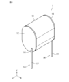
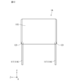
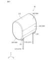
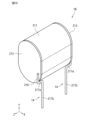
- FIG. 1 is a perspective view showing a film capacitor according to a first embodiment
- FIG. Front view of the film capacitor in Fig. 1 Side view of the film capacitor in Fig. 1
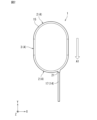
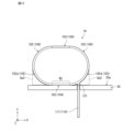
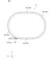
- Diagram of the film capacitor in Fig. 1 omitting the exterior material
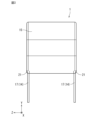
- Diagram of the film capacitor in Fig. 2 omitting the exterior material
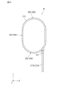
- Figure 3 omitting the exterior material of the film capacitor Front view when the film capacitor in Fig. 1 is mounted on a board
- Flowchart showing a method of manufacturing a film capacitor The figure which shows the state before immersing a laminated body in liquid resin.
- FIG. 4 is a perspective view showing a film capacitor according to a second embodiment; Front view of film capacitor in FIG. Side view of the film capacitor of FIG. The figure which shows the state which mounted the film capacitor of FIG. 10 on the board. The figure which shows the state which is immersing the laminated body in liquid resin.
- FIG. 4 is a perspective view showing a film capacitor according to a third embodiment; Front view of film capacitor in FIG. Side view of the film capacitor of FIG. Figure 15 omitting the exterior material of the film capacitor The figure which omitted the exterior material of the film capacitor of FIG. The figure which shows the state which is immersing the laminated body in liquid resin.
- FIG. 4 is a perspective view showing a film capacitor according to a fourth embodiment; Front view of film capacitor in FIG.
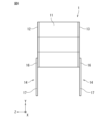
- FIG. 21 omitting the exterior material of the film capacitor
- the figure which omitted the exterior material of the film capacitor of FIG. FIG. 21 is a perspective view showing terminal electrodes of the film capacitor in FIG.
- a wound film capacitor formed by winding a dielectric film generally has rounded side surfaces. Therefore, when mounted on a board, the rounded portion becomes a dead space, which hinders the miniaturization of the device.
- the present inventors have studied a film capacitor in which terminal electrodes are arranged in a dead space when mounted on a substrate, and have arrived at the following invention.
- a film capacitor according to a first aspect of the present invention is a film capacitor to be mounted on a substrate, comprising a laminate of dielectric films, a first electrode formed on one end surface of the laminate, and the other end surface of the laminate. a connecting portion electrically connected to the first electrode or the second electrode; and an extending portion extending from the connecting portion toward the substrate in a direction along the first electrode or the second electrode.
- the film capacitor includes the first electrode and the second electrode It is formed in a columnar shape having a side surface that connects with the electrode, the side surface has a curved portion, and at least a part of the extending portion is aligned with a region of the curved portion facing the substrate and the substrate when the film capacitor is mounted on the substrate. in the space formed between and and at a position shifted from the position closest to the substrate in the curved portion.
- the distance between the film capacitor and the board when mounted on the board can be reduced, so the size and height of the device can be reduced.
- a portion of the exterior material that covers at least a portion of the stretched portion may be arranged in the space.
- the portion of the exterior material covering at least a portion of the extending portion may be arranged at a position farther from the substrate than a position of the curved portion closest to the substrate.
- the extending portion may include a first extending portion extending along the curved portion from the connecting portion and a second extending portion extending from the first extending portion toward the substrate. good.
- the interval between the terminal electrodes can be changed without increasing the mounting area.
- the terminal electrode may further have a substrate connecting portion extending from the extending portion in a direction along the substrate, and the substrate connecting portion may be arranged within the space.
- part of the side surface of the film capacitor may be in contact with the substrate.
- the number of contact points between the substrate and the film capacitor can be increased, so the stability when mounted on the substrate can be improved.
- the curved portion may have a diameter of 8 mm or more.
- the space formed between the substrate and the film capacitor can be widened, so it is possible to easily obtain the effect of lowering the height while reducing the mounting area.
- a method for manufacturing a film capacitor according to an eighth aspect of the present invention comprises the steps of: forming a laminate of dielectric films; forming external electrodes on both ends of the laminate; and an extending portion extending from the connection portion; immersing the laminate with the terminal electrodes connected to it in a liquid exterior material; and curing the exterior material, wherein the terminal electrode is
- the step of immersing the connected laminate in the liquid exterior material includes tilting the extending portions of the terminal electrodes from a direction perpendicular to the liquid surface of the exterior material.
- FIG. 1 is a perspective view showing a film capacitor 1 according to Embodiment 1.
- FIG. 2 is a front view of the film capacitor 1 of FIG. 1.
- FIG. 3 is a side view of the film capacitor 1 of FIG. 1.
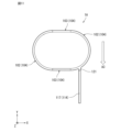
- FIG. 4 is a diagram of the film capacitor 1 of FIG. 1 with the exterior material 15 omitted.
- FIG. 5 is a diagram of the film capacitor 1 of FIG. 2 with the exterior material 15 omitted.
- FIG. 6 is a diagram of the film capacitor 1 of FIG. 3 with the exterior material 15 omitted.
- the X, Y, and Z directions in the figure indicate the horizontal direction, height direction, and vertical direction of the film capacitor 1, respectively.
- the film capacitor 1, as shown in FIGS. 1 to 3, is a columnar film capacitor having an oval cross section.
- the film capacitor 1 has a side surface 4 including two curved portions 2 and a flat portion 3 connecting the curved portions 2, and is formed in a columnar shape.
- the boundary between the curved portion 2 and the flat portion 3 in FIGS. may not be separated by boundaries. The same applies to the figures after FIG. 7 .
- the film capacitor 1 has a laminate 11 of dielectric films, a first electrode 12, a second electrode 13, and a terminal electrode 14, as shown in FIG. Moreover, the laminate 11 , the first electrode 12 , the second electrode 13 , and at least part of the terminal electrode 14 are covered with the exterior material 15 .
- the film capacitor 1 is mounted on a substrate 30 (see FIG. 7) through terminal electrodes 14 .
- the laminated body 11 of the film capacitor 1 of the present embodiment is formed by stacking and then winding dielectric films having a metal deposition film formed on the surface thereof. Therefore, the laminated body 11 may also be called a wound body. In the present embodiment, by pressing the wound body of the dielectric film into a flat shape, the laminate 11 is formed into a columnar shape having an oval cross section. The laminate 11 can also be formed by laminating dielectric films without winding them.
- a plastic film such as polyethylene terephthalate, polypropylene, polyphenylesulfide, or polyethylene naphthalate can be used.
- Metal such as Al and Zn can be used as the metal deposition film formed on the surface of the plastic film.
- a first electrode 12 is formed at one end of a laminate 11 of dielectric films, and a second electrode 13 is formed at the other end.
- the first electrode 12 and the second electrode 13 can be formed by thermally spraying Zn or the like on one end and the other end of the laminate 11 .
- the terminal electrodes 14 include two terminal electrodes 14 , one terminal electrode 14 electrically connected to the first electrode 12 and the other terminal electrode 14 electrically connected to the second electrode 13 .
- the terminal electrode 14 has a connection portion 16 electrically connected to the first electrode 12 or the second electrode 13, and a terminal electrode extending from the connection portion 16 along the first electrode 12 or the second electrode 13. and an extension 17 extending in the direction (arrow A1 in FIG. 2).
- the connecting portion 16 is connected to the first electrode 12 or the second electrode 13 by welding.
- the terminal electrode 14 is made of a conductive material such as a lead wire.
- the exterior material 15 is arranged to cover the laminate 11 , the first electrode 12 , the second electrode 13 , the connection portion 16 of the terminal electrode 14 , and at least part of the extension portion 17 of the terminal electrode 14 .
- a synthetic resin such as an epoxy resin can be used as the exterior material 15, for example.
- the exterior material 15 is a film capacitor (see FIG. 4) in which the first electrode 12 and the second electrode 13 are formed on the laminate 11 and the terminal electrode 14 is connected to the first electrode 12 and the second electrode 13, for example, by dipping. It can be formed by immersing it in a liquid resin by a coating method.
- the laminate 11 including the first electrode 12 and the second electrode 13 is covered with the resin, and furthermore, the connecting portion 16 of the terminal electrode 14 and the extending portion 17 of the terminal electrode 14 are formed.
- the resin adheres to at least a portion of the That is, as shown in FIGS. 9A to 9C, which will be described later, the exterior material 15 and the resin film 21 at the root of the extending portion 17 are formed together.
- the resin film 21 formed on the extended portion 17 is arranged in a dead space when the film capacitor 1 is mounted on the substrate.
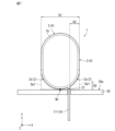
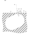
- FIG. 7 is a front view when the film capacitor 1 of FIG. 1 is mounted on the substrate 30.
- FIG. 7 film capacitor 1 is mounted on substrate 30 such that curved portion 2 of side surface 4 faces main surface 30 a of substrate 30 .
- a space Sp ⁇ b>1 is formed between the substrate 30 and the region 2 a facing the substrate 30 in the curved portion 2 . Since other components cannot be mounted in the space Sp1, the space Sp1 becomes a dead space on the substrate 30.
- terminal electrode 14 is formed such that at least part of extending portion 17 is arranged within space Sp1 when film capacitor 1 is mounted on substrate 30 . Furthermore, the extending portion 17 is pulled out to a position shifted from the position N1 closest to the substrate 30 in the bending portion 2 .
- the extension part 17 By arranging the extension part 17 in this way, the exterior material 15 can be formed so that the resin film 21 can be accommodated in the space Sp1 when the film capacitor 1 is mounted on the substrate 30 . Since the portion of the extending portion 17 where the resin film 21 is formed cannot be inserted into the through-hole of the substrate 30, the dead space is further reduced by forming the resin film 21 so as to fit in the space Sp1. be able to. Therefore, the dead space can be reduced, contributing to the miniaturization and low profile of the device.
- the resin film 21 is arranged at a position farther from the substrate 30 than the position N1 closest to the substrate 30 in the curved portion 2 (position away from the substrate 30 in the direction of the arrow A2). In other words, when the film capacitor 1 is mounted on the substrate 30 , the distance between the position N1 and the substrate 30 is smaller than the distance between the resin film 21 and the substrate 30 . By arranging the resin film 21 in such a manner, the dead space can be further reduced.
- the diameter D1 of the curved portion 2 is preferably 8 mm or more. As the diameter D1 of the curved portion 2 increases, the space Sp1 when the film capacitor 1 is mounted on the substrate 30 also increases. Therefore, the resin film 21 of the extending portion 17 can be easily accommodated in the space Sp1.
- the distance D2 from the extended portion 17 of the terminal electrode 14 to the flat portion 3 is preferably 1/4 or less of the diameter D1 of the curved portion 2 .
- the substrate 30 and the position N1 of the film capacitor 1 may be in contact with each other. In this case, since the contact points between the film capacitor 1 and the substrate 30 can be increased, the stability during mounting can be improved.
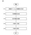
- FIG. 8 is a flow chart showing the manufacturing method of the film capacitor 1. As shown in FIG. A method of manufacturing the film capacitor 1 will be described with reference to FIG.
- a laminate 11 of dielectric films is formed (step S11).
- a laminate 11 having an elliptical cross section can be formed by rolling a dielectric film having a vapor-deposited metal film on its surface into a cylindrical shape, and then pressing it with a predetermined pressure.
- the first electrode 12 and the second electrode 13 are formed on both ends of the laminate 11 (step S12).
- the first electrode 12 and the second electrode 13 can be formed by spraying a metal such as Zn on both ends of the laminate 11 .
- the terminal electrode 14 is connected to the first electrode 12 and the second electrode 13 (step S13).
- the terminal electrode 14 is made of a conductive material such as a lead wire, and can be connected to the first electrode 12 and the second electrode 13 by welding.
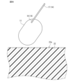
- FIG. 9A is a diagram showing a state before the laminate 11 is immersed in the liquid resin 22.
- FIG. 9B is a diagram showing a state in which the laminate 11 is immersed in a liquid exterior material. As shown in FIGS. 9A and 9B, when the laminate 11 is immersed in the liquid resin 22, it is preferable to incline the extending portion 17 from the normal line NL perpendicular to the liquid surface 22a of the resin 22.
- FIG. 9C is a diagram showing a state in which the laminate 11 immersed in the liquid resin 22 is pulled up.
- the resin film 21 is formed at the base of the extension portion 17 of the terminal electrode 14 by surface tension, as shown in FIG. 9C.
- step S15 the exterior material is cured (step S15) to complete the film capacitor 1.
- the completed film capacitor 1 is mounted on a substrate 30 as shown in FIG.
- the resin film 21 is formed so as to fit in the space Sp1 between the substrate 30 and the curved portion 2, as shown in FIG. .
- the film capacitor 1 includes a laminate 11, a first electrode 12, a second electrode 13, a terminal electrode 14, and an exterior material 15.
- the laminate 11 is formed by winding a dielectric film.
- the first electrode 12 is formed on one end surface of the laminate 11 .
- a second electrode 13 is formed on the other end surface of the laminate 11 .
- the terminal electrode 14 has a connection portion 16 and an extension portion 17 .
- the connecting portion 16 is electrically connected to the first electrode 12 or the second electrode 13 .
- Extension portion 17 extends from connection portion 16 toward substrate 30 in a direction along first electrode 12 or second electrode 13 .
- the exterior material 15 covers the first electrode 12 , the second electrode 13 , the connection portion 16 and at least part of the extension portion 17 .
- a film capacitor 1 is formed in a columnar shape having a side surface 4 connecting a first electrode 12 and a second electrode 13 , and the side surface 4 has a curved portion 2 . At least part of the extending portion 17 is within a space Sp1 formed between a region of the curved portion 2 facing the substrate 30 and the substrate 30 when the film capacitor 1 is mounted on the substrate 30, and It is arranged at a position shifted from the position closest to the substrate 30 in the curved portion 2 .
- a portion of the exterior material 15 that covers at least a portion of the extending portion 17 is arranged in the space Sp1.
- the resin film 21 is formed in the dead space (space Sp1) when the film capacitor 1 is mounted on the substrate 30. can be accommodated. Therefore, the mounting area when the film capacitor 1 is mounted on the substrate 30 can be reduced, and the height can be reduced.
- portion of the exterior material 15 that covers at least a portion of the extending portion 17 is arranged at a position farther from the substrate 30 than the position of the curved portion 2 closest to the substrate 30 .
- the resin film 21 can be accommodated in the dead space when the film capacitor 1 is mounted on the substrate 30. Therefore, it contributes to miniaturization and low profile of the device.
- part of the side surface 4 of the film capacitor 1 and the substrate 30 are in contact.
- the contact points between the film capacitor 1 and the substrate 30 can be increased, and the stability during mounting can be improved.
- the diameter of the curved portion 2 is 8 mm or more.
- the dead space when the film capacitor 1 is mounted on the substrate 30 becomes large, so the resin film 21 can be easily accommodated in the dead space, and further miniaturization and low profile can be achieved.
- the method for manufacturing the film capacitor 1 includes the steps of forming a laminate 11 of dielectric films, forming external electrodes 12 and 13 on both ends of the laminate 11, and connecting the external electrodes 12 and 13 to the external electrodes. a step of connecting the terminal electrode 14 having the portion 16 and the extension portion 17 extending from the connection portion 16; a step of immersing the laminate 11 to which the terminal electrode 14 is connected in a liquid resin 22; and a step of curing the resin 22. ,including.
- the step of immersing the laminate 11 to which the terminal electrodes 14 are connected in the liquid resin 22 includes tilting the extending portions 17 of the terminal electrodes 14 from a direction perpendicular to the liquid surface 22 a of the resin 22 .
- the columnar film capacitor 1 having an oval cross section has been described as an example, but the shape of the film capacitor 1 is not limited to this.
- any shape having a curved side surface such as a columnar shape or an elliptical columnar shape may be used.
- the exterior material 15 can be formed by a method including a step of immersing in a liquid.
- the terminal electrodes 14 are formed of lead wires, but the present invention is not limited to this.
- the terminal electrodes 14 may be formed of flat terminals.
- the terminal electrode 14 may be connected to the first electrode 12 or the second electrode 13 by soldering.
- FIG. 10 is a perspective view showing a film capacitor according to Embodiment 2.
- FIG. 11 is a front view of the film capacitor of FIG. 10.
- FIG. 12 is a side view of the film capacitor of FIG. 10.
- FIG. 13 is a diagram showing a state in which the film capacitor of FIG. 10 is mounted on a substrate.
- the X, Y, and Z directions in the drawing indicate the horizontal direction, height direction, and vertical direction of the film capacitor 1A, respectively.
- the extending direction of the extending portion 117 is different from that in the first embodiment.
- the extended portions 17 of the terminal electrodes 14 are formed to extend in the direction along the flat portion 3, but in the film capacitor 1A of Embodiment 2, the extended portions 117 are formed along the flat portions 103 (arrow A3 in FIG. 11). Since extended portion 117 is arranged in this manner, film capacitor 1A of the second embodiment is mounted on the substrate such that flat portion 103 faces main surface 30a of substrate 30, as shown in FIG.
- the position N2 closest to the substrate 30 is the flat portion 103 facing the main surface 30a of the substrate 30.
- the extending portion 117 is arranged at a position shifted from the position N2, when the film capacitor 1A is mounted on the substrate 30, the resin film 121 of the exterior material 115 extends to the area 102a of the curved portion 102 facing the substrate 30. and the substrate 30 so as to be accommodated in the space Sp2.
- FIG. 14 is a diagram showing a state in which the laminate 111 in which terminal electrodes are connected to each of the first electrode and the second electrode is immersed in the liquid resin 22 .
- the laminate 111 is immersed in the resin 22 so that the extended portion 117 is inclined at an angle ⁇ 2 with respect to the normal line NL perpendicular to the liquid surface 22a of the liquid resin 22 .
- the resin film 121 can be formed so as to fit in the space Sp2.
- the flat portion 103 is arranged to face the main surface 30a of the substrate 30, the stability during mounting can be improved. In addition, the height can be further reduced.
- Embodiment 3 differences from Embodiment 1 will be mainly described.
- the same reference numerals are assigned to the same or equivalent configurations as in the first embodiment.
- the description overlapping with that in the first embodiment is omitted.
- FIG. 15 is a perspective view showing a film capacitor 1B according to Embodiment 3.
- FIG. 16 is a front view of the film capacitor 1B of FIG. 15.
- FIG. 17 is a side view of the film capacitor 1B of FIG. 15.
- FIG. 18 is a diagram of the film capacitor 1B of FIG. 15 with the exterior material 215 omitted.
- FIG. 19 is a diagram of the film capacitor 1B of FIG. 17 with the exterior material 215 omitted.
- the shape of terminal electrodes 214 is different from that in the first embodiment.
- the extending portions of the terminal electrode 214 include a first extending portion 217a extending from the connecting portion 216 along the curved portion 202 of the film capacitor 1B, and extending from the first extending portion 217a toward the substrate (not shown). and a second extending portion 217b.
- the terminal electrode 214 can form a connecting portion 216, a first extending portion 217a, and a second extending portion 217b by bending a lead wire or the like, for example.
- the connecting portion 216 of the terminal electrode 214, on which the connecting portion 216, the first extending portion 217a, and the second extending portion 217b are formed in advance, is attached by welding to the first electrode 212 and the second electrode 213 at both ends of the laminate 211. can be done.
- the interval between the two terminal electrodes 214 connected to the first electrode 212 and the second electrode 213 can be changed. can.
- the first extending portion 217a extends from the connecting portion 216 along the curved portion 202, when the film capacitor 1B is mounted on the substrate, the resin film 221 formed on the first extending portion 217a and the curved portion 202 are separated from each other. is placed in the space formed between Therefore, it is possible to change the interval between the terminal electrodes 214 while accommodating the resin film 221 in the dead space, thereby improving the degree of freedom in design.
- FIG. 20 is a diagram showing a state in which a laminate 211 in which terminal electrodes are connected to each of the first electrode and the second electrode is immersed in the liquid resin 22 .
- the laminate 111 is immersed in the resin 22 so that the extended portion 117 is inclined at an angle ⁇ 3 with respect to the normal line NL perpendicular to the liquid surface 22a of the liquid resin 22 .
- the first extending portion 217 a is immersed in the resin 22 .
- the exterior material 215 is formed in this way, the resin film 221 can be formed so as to fit in the dead space.
- the extending portions include a first extending portion 217a extending from the connecting portion 216 along the curved portion 202 and a second extending portion 217b extending from the first extending portion 217a toward the substrate.
- the interval between the terminal electrodes 214 can be changed without increasing the mounting area, so the degree of freedom in design can be improved.
- Embodiment 4 mainly different points from Embodiment 1 will be described.
- the same reference numerals are given to the same or equivalent configurations as in the first embodiment. Further, in the fourth embodiment, the description overlapping with the first embodiment is omitted.
- FIG. 21 is a perspective view showing a film capacitor 1C according to Embodiment 4.
- FIG. 22 is a front view of the film capacitor 1C of FIG. 21.
- FIG. FIG. 23 is a diagram of the film capacitor 1C of FIG. 21 with the exterior material 315 omitted.
- FIG. 24 is a diagram of the film capacitor in FIG. 22 with the exterior material 315 omitted.
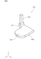
- FIG. 25 is a perspective view showing terminal electrodes 314 of the film capacitor of FIG.
- Embodiment 4 differs from Embodiment 1 in that the terminal electrode 314 has a substrate connection portion 318 . Specifically, as shown in FIGS. 21 to 24, the terminal electrode 314 further has a substrate connecting portion 318 extending from the extending portion 317 in the direction along the substrate 31 (see FIG. 27). A resin film 321 is formed on at least part of the extending portion 317 .
- the terminal electrode 314 is formed in a shape having a connection portion 316, an extension portion 317, and a substrate connection portion 318, as shown in FIG.
- the board connection portion 318 is formed in a plate shape.
- the terminal electrode 314 can be formed, for example, by bending a metal plate cut into a predetermined shape by press working.
- FIG. 26 is a diagram showing a state in which the laminate 311 in which the terminal electrodes 314 are connected to the first electrodes 312 and the second electrodes 313 is immersed in the liquid resin 22 .
- the substrate connection portion 318 is immersed in the resin 22 so as to be inclined at an angle ⁇ 4 with respect to the normal line NL perpendicular to the liquid surface 22a of the liquid resin 22 .
- the angle ⁇ 4 can be appropriately adjusted depending on the shape or size of the film capacitor.
- the exterior material 315 By forming the exterior material 315 in this way, it is possible to suppress the generation of the resin film 321 on the main surface 318a (see FIG. 25) of the substrate connecting portion 318 connected to the substrate 31.
- FIG. By forming the resin 22 in this manner, at least a portion of the connection portion 316 and the extension portion 317 of the terminal electrode 314 is covered with the resin.
- FIG. 27 is a diagram showing a state in which the film capacitor 1C of FIG. 21 is mounted on the substrate 31.
- the film capacitor 1C is mounted on the substrate 31 by surface mounting.
- the terminal electrode 314 is arranged so as to be accommodated in a space Sp3 formed between a region 302a of the curved portion 302 facing the substrate 31 and the principal surface 31a of the substrate 31 . Therefore, the film capacitor 1C suitable for surface mounting can be provided without increasing the mounting area.
- the terminal electrode 314 further has a substrate connecting portion 318 extending from the extending portion 317 in the direction along the substrate 31 .
- the board connection portion 318 is arranged in the space Sp3.
- the present invention is useful for capacitors used in various electronic devices, electrical devices, industrial devices, vehicle devices, and the like.
Landscapes
- Engineering & Computer Science (AREA)
- Power Engineering (AREA)
- Microelectronics & Electronic Packaging (AREA)
- Manufacturing & Machinery (AREA)
- Fixed Capacitors And Capacitor Manufacturing Machines (AREA)
Priority Applications (3)
| Application Number | Priority Date | Filing Date | Title |
|---|---|---|---|
| CN202280079201.8A CN118339625A (zh) | 2021-12-01 | 2022-10-14 | 薄膜电容器以及薄膜电容器的制造方法 |
| JP2023564782A JP7772087B2 (ja) | 2021-12-01 | 2022-10-14 | フィルムコンデンサおよびフィルムコンデンサの製造方法 |
| US18/677,315 US20240312724A1 (en) | 2021-12-01 | 2024-05-29 | Film capacitor and method for producing film capacitor |
Applications Claiming Priority (2)
| Application Number | Priority Date | Filing Date | Title |
|---|---|---|---|
| JP2021-195396 | 2021-12-01 | ||
| JP2021195396 | 2021-12-01 |
Related Child Applications (1)
| Application Number | Title | Priority Date | Filing Date |
|---|---|---|---|
| US18/677,315 Continuation US20240312724A1 (en) | 2021-12-01 | 2024-05-29 | Film capacitor and method for producing film capacitor |
Publications (1)
| Publication Number | Publication Date |
|---|---|
| WO2023100502A1 true WO2023100502A1 (ja) | 2023-06-08 |
Family
ID=86611958
Family Applications (1)
| Application Number | Title | Priority Date | Filing Date |
|---|---|---|---|
| PCT/JP2022/038446 Ceased WO2023100502A1 (ja) | 2021-12-01 | 2022-10-14 | フィルムコンデンサおよびフィルムコンデンサの製造方法 |
Country Status (4)
| Country | Link |
|---|---|
| US (1) | US20240312724A1 (cg-RX-API-DMAC7.html) |
| JP (1) | JP7772087B2 (cg-RX-API-DMAC7.html) |
| CN (1) | CN118339625A (cg-RX-API-DMAC7.html) |
| WO (1) | WO2023100502A1 (cg-RX-API-DMAC7.html) |
Citations (5)
| Publication number | Priority date | Publication date | Assignee | Title |
|---|---|---|---|---|
| JPH02155215A (ja) * | 1988-12-08 | 1990-06-14 | Nitsuko Corp | 低背形フィルムコンデンサの製造方法 |
| JPH02240907A (ja) * | 1989-03-15 | 1990-09-25 | Nitsuko Corp | メタライズドフィルムコンデンサのリード線引出し方法 |
| JPH0645178A (ja) * | 1992-07-24 | 1994-02-18 | Nissei Denki Kk | 電子部品 |
| JP3025930U (ja) * | 1995-12-15 | 1996-06-25 | 富士通東和エレクトロン株式会社 | チップ型フィルムコンデンサ |
| WO2019087260A1 (ja) * | 2017-10-30 | 2019-05-09 | 日立化成株式会社 | フィルムコンデンサの製造方法及びケース |
-
2022
- 2022-10-14 WO PCT/JP2022/038446 patent/WO2023100502A1/ja not_active Ceased
- 2022-10-14 JP JP2023564782A patent/JP7772087B2/ja active Active
- 2022-10-14 CN CN202280079201.8A patent/CN118339625A/zh active Pending
-
2024
- 2024-05-29 US US18/677,315 patent/US20240312724A1/en active Pending
Patent Citations (5)
| Publication number | Priority date | Publication date | Assignee | Title |
|---|---|---|---|---|
| JPH02155215A (ja) * | 1988-12-08 | 1990-06-14 | Nitsuko Corp | 低背形フィルムコンデンサの製造方法 |
| JPH02240907A (ja) * | 1989-03-15 | 1990-09-25 | Nitsuko Corp | メタライズドフィルムコンデンサのリード線引出し方法 |
| JPH0645178A (ja) * | 1992-07-24 | 1994-02-18 | Nissei Denki Kk | 電子部品 |
| JP3025930U (ja) * | 1995-12-15 | 1996-06-25 | 富士通東和エレクトロン株式会社 | チップ型フィルムコンデンサ |
| WO2019087260A1 (ja) * | 2017-10-30 | 2019-05-09 | 日立化成株式会社 | フィルムコンデンサの製造方法及びケース |
Also Published As
| Publication number | Publication date |
|---|---|
| US20240312724A1 (en) | 2024-09-19 |
| JP7772087B2 (ja) | 2025-11-18 |
| CN118339625A (zh) | 2024-07-12 |
| JPWO2023100502A1 (cg-RX-API-DMAC7.html) | 2023-06-08 |
Similar Documents
| Publication | Publication Date | Title |
|---|---|---|
| US12293881B2 (en) | Electrolytic capacitor and method for producing same | |
| US6680841B2 (en) | Solid electrolytic capacitor and its manufacturing method | |
| CN1210734C (zh) | 电容器 | |
| US6920037B2 (en) | Solid electrolytic capacitor | |
| JP7113285B2 (ja) | 電解コンデンサ | |
| US6765784B2 (en) | Solid electrolytic capacitor and manufacturing method for the same | |
| US20240371574A1 (en) | Capacitor module and method for fabricating capacitor module | |
| JP2002324727A (ja) | コンデンサ | |
| JP4458470B2 (ja) | 積層型固体電解コンデンサ及びその製造方法 | |
| WO2011040352A1 (ja) | 電解コンデンサ | |
| WO2023100502A1 (ja) | フィルムコンデンサおよびフィルムコンデンサの製造方法 | |
| US12374505B2 (en) | Electrolytic capacitor | |
| CN102222570B (zh) | 电解电容器及其制造方法 | |
| JP2019192787A (ja) | 電子部品 | |
| JP4215250B2 (ja) | チップ型固体電解コンデンサ及びその製造方法 | |
| JP2010021318A (ja) | 電子部品およびその製造方法 | |
| JP2009272461A (ja) | フィルムコンデンサ | |
| US12518930B2 (en) | Multilayer ceramic capacitor including SiO2 film on surfaces thereof | |
| US20250014823A1 (en) | Film capacitor | |
| JPH05283300A (ja) | 固体電解コンデンサ | |
| JP2021057487A (ja) | フィルムコンデンサ | |
| JPH06176978A (ja) | 固体電解コンデンサ | |
| JP2009152431A (ja) | フィルムコンデンサ | |
| JPH05144687A (ja) | 固体電解コンデンサの製造方法 | |
| KR19990016347A (ko) | 권취형 고체 전해 콘덴서 |
Legal Events
| Date | Code | Title | Description |
|---|---|---|---|
| 121 | Ep: the epo has been informed by wipo that ep was designated in this application |
Ref document number: 22900936 Country of ref document: EP Kind code of ref document: A1 |
|
| ENP | Entry into the national phase |
Ref document number: 2023564782 Country of ref document: JP Kind code of ref document: A |
|
| WWE | Wipo information: entry into national phase |
Ref document number: 202280079201.8 Country of ref document: CN |
|
| NENP | Non-entry into the national phase |
Ref country code: DE |
|
| 122 | Ep: pct application non-entry in european phase |
Ref document number: 22900936 Country of ref document: EP Kind code of ref document: A1 |