WO2023095396A1 - ジャンクションバリアショットキーダイオード - Google Patents
ジャンクションバリアショットキーダイオード Download PDFInfo
- Publication number
- WO2023095396A1 WO2023095396A1 PCT/JP2022/030766 JP2022030766W WO2023095396A1 WO 2023095396 A1 WO2023095396 A1 WO 2023095396A1 JP 2022030766 W JP2022030766 W JP 2022030766W WO 2023095396 A1 WO2023095396 A1 WO 2023095396A1
- Authority
- WO
- WIPO (PCT)
- Prior art keywords
- anode electrode
- trench
- schottky diode
- junction barrier
- drift layer
- Prior art date
- Legal status (The legal status is an assumption and is not a legal conclusion. Google has not performed a legal analysis and makes no representation as to the accuracy of the status listed.)
- Ceased
Links
Images


Classifications
-
- H—ELECTRICITY
- H10—SEMICONDUCTOR DEVICES; ELECTRIC SOLID-STATE DEVICES NOT OTHERWISE PROVIDED FOR
- H10D—INORGANIC ELECTRIC SEMICONDUCTOR DEVICES
- H10D8/00—Diodes
- H10D8/60—Schottky-barrier diodes
- H10D8/605—Schottky-barrier diodes of the trench conductor-insulator-semiconductor barrier type, e.g. trench MOS barrier Schottky rectifiers [TMBS]
-
- H—ELECTRICITY
- H10—SEMICONDUCTOR DEVICES; ELECTRIC SOLID-STATE DEVICES NOT OTHERWISE PROVIDED FOR
- H10D—INORGANIC ELECTRIC SEMICONDUCTOR DEVICES
- H10D62/00—Semiconductor bodies, or regions thereof, of devices having potential barriers
- H10D62/10—Shapes, relative sizes or dispositions of the regions of the semiconductor bodies; Shapes of the semiconductor bodies
- H10D62/102—Constructional design considerations for preventing surface leakage or controlling electric field concentration
- H10D62/103—Constructional design considerations for preventing surface leakage or controlling electric field concentration for increasing or controlling the breakdown voltage of reverse-biased devices
- H10D62/105—Constructional design considerations for preventing surface leakage or controlling electric field concentration for increasing or controlling the breakdown voltage of reverse-biased devices by having particular doping profiles, shapes or arrangements of PN junctions; by having supplementary regions, e.g. junction termination extension [JTE]
- H10D62/106—Constructional design considerations for preventing surface leakage or controlling electric field concentration for increasing or controlling the breakdown voltage of reverse-biased devices by having particular doping profiles, shapes or arrangements of PN junctions; by having supplementary regions, e.g. junction termination extension [JTE] having supplementary regions doped oppositely to or in rectifying contact with regions of the semiconductor bodies, e.g. guard rings with PN or Schottky junctions
-
- H—ELECTRICITY
- H10—SEMICONDUCTOR DEVICES; ELECTRIC SOLID-STATE DEVICES NOT OTHERWISE PROVIDED FOR
- H10D—INORGANIC ELECTRIC SEMICONDUCTOR DEVICES
- H10D64/00—Electrodes of devices having potential barriers
- H10D64/20—Electrodes characterised by their shapes, relative sizes or dispositions
-
- H—ELECTRICITY
- H10—SEMICONDUCTOR DEVICES; ELECTRIC SOLID-STATE DEVICES NOT OTHERWISE PROVIDED FOR
- H10D—INORGANIC ELECTRIC SEMICONDUCTOR DEVICES
- H10D64/00—Electrodes of devices having potential barriers
- H10D64/60—Electrodes characterised by their materials
- H10D64/64—Electrodes comprising a Schottky barrier to a semiconductor
-
- H—ELECTRICITY
- H10—SEMICONDUCTOR DEVICES; ELECTRIC SOLID-STATE DEVICES NOT OTHERWISE PROVIDED FOR
- H10D—INORGANIC ELECTRIC SEMICONDUCTOR DEVICES
- H10D8/00—Diodes
- H10D8/50—PIN diodes
-
- H—ELECTRICITY
- H10—SEMICONDUCTOR DEVICES; ELECTRIC SOLID-STATE DEVICES NOT OTHERWISE PROVIDED FOR
- H10D—INORGANIC ELECTRIC SEMICONDUCTOR DEVICES
- H10D8/00—Diodes
- H10D8/60—Schottky-barrier diodes
-
- H—ELECTRICITY
- H10—SEMICONDUCTOR DEVICES; ELECTRIC SOLID-STATE DEVICES NOT OTHERWISE PROVIDED FOR
- H10D—INORGANIC ELECTRIC SEMICONDUCTOR DEVICES
- H10D99/00—Subject matter not provided for in other groups of this subclass
Definitions
- the present invention relates to junction barrier Schottky diodes, and more particularly to junction barrier Schottky diodes using gallium oxide.
- a Schottky barrier diode is a rectifying element that utilizes a Schottky barrier formed by a junction between a metal and a semiconductor, and is characterized by a lower forward voltage and a faster switching speed than ordinary diodes having a PN junction. are doing. Therefore, Schottky barrier diodes are sometimes used as switching elements for power devices.
- gallium oxide has a very large bandgap of 4.8 to 4.9 eV and a large dielectric breakdown field of approximately 8 MV/cm. It is very promising as a device.
- An example of a Schottky barrier diode using gallium oxide is described in Patent Document 1.
- Patent Document 1 discloses a junction barrier Schottky diode having a structure in which a plurality of trenches provided in a gallium oxide layer are filled with a p-type semiconductor material.
- the junction barrier Schottky diode described in Patent Document 1 has a problem of high on-resistance due to the small area of Schottky contact between the anode electrode and the drift layer.
- the impurity concentration of the drift layer may be increased, but in this case the reverse withstand voltage is lowered.
- an object of the present invention is to reduce the on-resistance while ensuring a sufficient reverse breakdown voltage in a junction barrier Schottky diode using gallium oxide.
- a junction barrier Schottky diode comprises a semiconductor substrate made of gallium oxide, a drift layer made of gallium oxide provided on the semiconductor substrate, an anode electrode in Schottky contact with the drift layer, and an ohmic contact with the semiconductor substrate.
- the anode electrode embedded in the central trench is in Schottky contact with the side surface of the central trench, it is possible to reduce the on-resistance without increasing the impurity concentration of the drift layer.
- the anode electrodes are a first anode electrode in Schottky contact with the upper surface of the drift layer and a second anode electrode in Schottky contact with the side surface of the central trench and made of a metal material different from that of the first anode electrode. and electrodes. This makes it easier to produce an anode electrode without voids.
- the drift layer may further have a peripheral trench surrounding the central trench, and the bottom surface and peripheral side surfaces of the peripheral trench may be in contact with the semiconductor material without being in contact with the anode electrode. According to this, the electric field generated at the outer peripheral bottom portion of the outer peripheral trench when a reverse voltage is applied is alleviated. In this case, at least part of the inner peripheral side surface of the outer trench may be in Schottky contact with the anode electrode. According to this, since the area of Schottky contact is enlarged, it is possible to further reduce the on-resistance.
- the drift layer may further have a peripheral trench in which the anode electrode is embedded and which surrounds the central trench, and the inner wall of the peripheral trench may be covered with an insulating film without being in contact with the anode electrode. According to this, the electric field generated at the outer peripheral bottom portion of the outer peripheral trench when a reverse voltage is applied is alleviated.
- the side surface of the central trench is in Schottky contact with the anode electrode, it is possible to reduce the on-resistance of the junction barrier Schottky diode using gallium oxide.
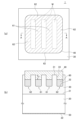
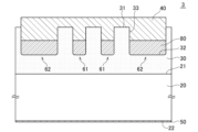
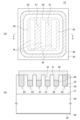
- FIG. 1(a) is a schematic plan view showing the configuration of a junction barrier Schottky diode 1 according to a first embodiment of the present invention.
- FIG. 1(b) is a schematic cross-sectional view along line AA shown in FIG. 1(a).
- FIGS. 2A to 2C are schematic cross-sectional views for explaining the positions of the inner walls of the central trench 61 and the peripheral trench 62 that are covered with the p-type semiconductor material 80.
- FIG. FIG. 3 is a schematic cross-sectional view showing the configuration of a junction barrier Schottky diode 2 according to a second embodiment of the invention.
- FIG. 4 is a schematic cross-sectional view showing the structure of a junction barrier Schottky diode 3 according to a third embodiment of the invention.
- FIG. 5 is a schematic cross-sectional view showing the structure of a junction barrier Schottky diode 4 according to a fourth embodiment of the invention.
- FIG. 6 is a schematic cross-sectional view showing the structure of a junction barrier Schottky diode 5 according to a fifth embodiment of the invention.
- FIG. 7 is a schematic cross-sectional view showing the structure of a junction barrier Schottky diode 6 according to a sixth embodiment of the invention.
- FIG. 8(a) is a schematic plan view showing the configuration of a junction barrier Schottky diode 7 according to a seventh embodiment of the present invention.
- FIG. 8(b) is a schematic cross-sectional view along line AA shown in FIG. 8(a).
- FIG. 8(a) is a schematic cross-sectional view along line AA shown in FIG. 8(a).
- FIG. 9 is a schematic cross-sectional view showing the structure of a junction barrier Schottky diode 8 according to an eighth embodiment of the invention.
- FIG. 10 is a schematic cross-sectional view showing the structure of a junction barrier Schottky diode 9 according to the ninth embodiment of the invention.
- FIG. 11 is a schematic cross-sectional view showing the structure of a junction barrier Schottky diode 10 according to a tenth embodiment of the invention.
- FIG. 12 is a schematic cross-sectional view showing the structure of a junction barrier Schottky diode 11 according to the eleventh embodiment of the invention.
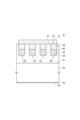
- FIG. 13(a) is a schematic plan view showing the configuration of a junction barrier Schottky diode 12 according to the twelfth embodiment of the present invention.
- FIG. 13(b) is a schematic cross-sectional view along line AA shown in FIG. 13(a).
- FIG. 14(a) is a schematic plan view showing the configuration of a junction barrier Schottky diode 13 according to the thirteenth embodiment of the present invention.
- FIG. 14(b) is a schematic cross-sectional view taken along line AA shown in FIG. 14(a).
- FIG. 15(a) is a schematic plan view showing the configuration of a junction barrier Schottky diode 14 according to the fourteenth embodiment of the present invention.
- FIG. 15(b) is a schematic cross-sectional view along line AA shown in FIG. 15(a).
- FIG. 16 is a schematic cross-sectional view showing the structure of a junction barrier Schottky diode 15 according to a fifteenth embodiment of the invention.
- FIG. 17 is a graph showing simulation results of the example.
- FIG. 1(a) is a schematic plan view showing the configuration of a junction barrier Schottky diode 1 according to a first embodiment of the present invention.
- FIG. 1(b) is a schematic cross-sectional view along line AA shown in FIG. 1(a).
- the junction barrier Schottky diode 1 includes a semiconductor substrate 20 and a drift layer 30 both made of gallium oxide ( ⁇ -Ga 2 O 3 ). Silicon (Si) or tin (Sn) is introduced into the semiconductor substrate 20 and the drift layer 30 as an n-type dopant.
- the dopant concentration is higher in the semiconductor substrate 20 than in the drift layer 30, so that the semiconductor substrate 20 functions as an n + layer and the drift layer 30 functions as an n ⁇ layer.
- the semiconductor substrate 20 is obtained by cutting a bulk crystal formed using a melt growth method or the like, and its thickness is about 250 ⁇ m.
- the planar size of the semiconductor substrate 20 is not particularly limited, but is generally selected according to the amount of current flowing through the element. It may be about 2.4 mm.
- the semiconductor substrate 20 has an upper surface 21 positioned on the upper surface side during mounting, and a back surface 22 positioned on the lower surface side during mounting on the opposite side of the upper surface 21 .
- a drift layer 30 is formed on the entire upper surface 21 .
- the drift layer 30 is a thin film obtained by epitaxially growing gallium oxide on the upper surface 21 of the semiconductor substrate 20 using reactive sputtering, PLD, MBE, MOCVD, HVPE, or the like. Although the thickness of the drift layer 30 is not particularly limited, it is generally selected according to the reverse withstand voltage of the device.
- An anode electrode 40 is formed on the upper surface 31 of the drift layer 30 to make Schottky contact with the drift layer 30 .
- the anode electrode 40 is made of metal such as platinum (Pt), palladium (Pd), gold (Au), nickel (Ni), molybdenum (Mo), and copper (Cu).
- the anode electrode 40 may be a multi-layer structure in which different metal films are laminated, such as Pt/Au, Pt/Al, Pd/Au, Pd/Al, Pt/Ti/Au or Pd/Ti/Au.
- the back surface 22 of the semiconductor substrate 20 is provided with a cathode electrode 50 that makes ohmic contact with the semiconductor substrate 20 .
- the cathode electrode 50 is made of metal such as titanium (Ti).
- the cathode electrode 50 may have a multi-layer structure in which different metal films are laminated, such as Ti/Au or Ti/Al.
- the drift layer 30 is provided with a central trench 61 and a peripheral trench 62 . Both the central trench 61 and the peripheral trench 62 are provided at positions overlapping with the anode electrode 40 in plan view, and are filled with the same metal material as the anode electrode 40 and the p-type semiconductor material 80 .
- a p-type semiconductor material 80 is in contact with the anode electrode 40 .
- Si, GaAs, GaN, SiC, Ge, ZnSe, CdS, InP, SiGe, AlN, BN, AlGaN, NiO, Cu2O , Ir2O3 , and Ag2O are used as the p-type semiconductor material 80.
- Center trench 61 is sandwiched between mesa regions M that are part of drift layer 30 .
- the outer trench 62 surrounds the mesa region M and the central trench 61 in a ring shape.
- the central trench 61 and the peripheral trench 62 do not need to be completely separated, and may be connected to each other as shown in FIG. 1(a).
- the central trench 61 and the peripheral trench 62 may have the same depth or may have different depths.
- the mesa region M is a part of the drift layer 30 defined by the central trench 61 and the peripheral trench 62 and becomes a depletion layer when a reverse voltage is applied between the anode electrode 40 and the cathode electrode 50 .
- the channel region of the drift layer 30 is pinched off, thereby greatly suppressing leakage current when a reverse voltage is applied.
- a p-type semiconductor material 80 is embedded in the bottom of the central trench 61 and the peripheral trench 62
- an anode electrode 40 is embedded in the upper part of the central trench 61 and the peripheral trench 62 . Therefore, among the inner walls of the central trench 61 and the peripheral trench 62, lower portions of the bottom surface 32 and the side surfaces 33 are in contact with the p-type semiconductor material 80, and among the inner walls of the central trench 61 and the peripheral trench 62, upper portions of the side surfaces 33 are in contact with the p-type semiconductor material 80. It is in contact with the anode electrode 40 .
- the drift layer 30 and the anode electrode 40 are in Schottky contact not only at the upper surface 31 of the drift layer 30 but also at the upper portions of the side surfaces 33 of the central trench 61 and the peripheral trench 62 . are all buried with the p-type semiconductor material 80, the on-resistance is reduced.
- the dopant concentration of the drift layer 30 can be suppressed to about 3 ⁇ 10 16 cm ⁇ 3 , a decrease in reverse withstand voltage is also prevented.
- FIG. 2A when the bottom surfaces 32 of the central trench 61 and the peripheral trench 62 are horizontal, and the portions located between the horizontal bottom surfaces 32 and the vertical side surfaces 33 are the curved surfaces 34. , the bottom surface 32 and the curved surface 34 must be covered with a p-type semiconductor material 80 .
- FIG. 2B when the bottom surfaces 32 of the central trench 61 and the peripheral trench 62 are curved as a whole, the entire curved bottom surfaces 32 need to be covered with the p-type semiconductor material 80.
- FIG. 2B when the bottom surfaces 32 of the central trench 61 and the peripheral trench 62 are curved as a whole, the entire curved bottom surfaces 32 need to be covered with the p-type semiconductor material 80.
- the anode electrode 40 is in Schottky contact with the upper portion of the side surface 33 of the central trench 61 and the peripheral trench 62, so that the central trench 61 and the peripheral trench 62 are all p
- the on-resistance can be reduced as compared with the case of embedding with the semiconductor material 80 of the mold.
- FIG. 3 is a schematic cross-sectional view showing the configuration of a junction barrier Schottky diode 2 according to a second embodiment of the invention.
- the junction barrier Schottky diode 2 includes a film of a p-type semiconductor material 80 that covers the lower portions of the bottom surface 32 and side surfaces 33 of the inner walls of the central trench 61 and the peripheral trench 62. It is different from the junction barrier Schottky diode 1 according to the first embodiment in that the thickness is small, so that the anode electrode 40 is also buried in the bottoms of the central trench 61 and the peripheral trench 62 . Since other basic configurations are the same as those of the junction barrier Schottky diode 1 according to the first embodiment, the same elements are denoted by the same reference numerals, and overlapping descriptions are omitted. As illustrated in this embodiment, the p-type semiconductor material 80 need not fill the entire bottom of the central trench 61 and the outer peripheral trench 62, and may cover only the surfaces thereof.
- FIG. 4 is a schematic cross-sectional view showing the structure of a junction barrier Schottky diode 3 according to a third embodiment of the invention.
- the width of the peripheral trench 62 is wider than the width of the central trench 61. It differs from the key diode 1. Since other basic configurations are the same as those of the junction barrier Schottky diode 1 according to the first embodiment, the same elements are denoted by the same reference numerals, and overlapping descriptions are omitted. By increasing the width of the outer trench 62 in this way, it is possible to alleviate the electric field concentrated near the bottom of the outer trench 62 when a reverse voltage is applied.
- FIG. 5 is a schematic cross-sectional view showing the structure of a junction barrier Schottky diode 4 according to a fourth embodiment of the invention.
- the junction barrier Schottky diode 4 according to the fourth embodiment differs from the junction barrier Schottky diode 4 according to the first embodiment in that the drift layer 30 located outside the outer peripheral trench 62 is removed.
- Diode 1 is different. Since other basic configurations are the same as those of the junction barrier Schottky diode 1 according to the first embodiment, the same elements are denoted by the same reference numerals, and overlapping descriptions are omitted. Since almost no on-current flows in the portion of the drift layer 30 located outside the outer peripheral trench 62, the drift layer 30 located in this portion may be removed as exemplified in this embodiment.
- FIG. 6 is a schematic cross-sectional view showing the structure of a junction barrier Schottky diode 5 according to a fifth embodiment of the invention.
- an insulating film 71 is provided between the upper surface 31 of the drift layer 30 located outside the peripheral trench 62 and the anode electrode 40. In this point, it differs from the junction barrier Schottky diode 1 according to the first embodiment. Since other basic configurations are the same as those of the junction barrier Schottky diode 1 according to the first embodiment, the same elements are denoted by the same reference numerals, and overlapping descriptions are omitted.
- As a material for the insulating film 71 it is desirable to use a material having a high withstand voltage such as SiO 2 or Al 2 O 3 . According to this, the pressure resistance effect is enhanced. According to the present embodiment, a so-called field plate structure is obtained by the insulating film 71, so that the electric field applied to the bottom of the outer peripheral trench 62 can be further relaxed.
- FIG. 7 is a schematic cross-sectional view showing the structure of a junction barrier Schottky diode 6 according to a sixth embodiment of the invention.
- the anode electrode 41 covering the upper surface of the drift layer 30 and the anode electrode 42 embedded in the central trench 61 and the peripheral trench 62 are made of different metals. It differs from the junction barrier Schottky diode 1 according to the first embodiment in that it is made of material. Since other basic configurations are the same as those of the junction barrier Schottky diode 1 according to the first embodiment, the same elements are denoted by the same reference numerals, and overlapping descriptions are omitted.
- Such a structure can be obtained, for example, by forming the anode electrode 42 by electrolytic plating and forming the anode electrode 41 by vapor deposition. According to such a manufacturing method, voids are less likely to occur in the anode electrode 42 embedded in the central trench 61 and the peripheral trench 62 .
- FIG. 8(a) is a schematic plan view showing the configuration of a junction barrier Schottky diode 7 according to a seventh embodiment of the present invention.
- FIG. 8(b) is a schematic cross-sectional view along line AA shown in FIG. 8(a).
- the junction barrier Schottky diode 7 according to the seventh embodiment has a junction barrier shot similar to that of the first embodiment in that the entire outer trench 62 is filled with a p-type semiconductor material 80 . It differs from the key diode 1. Since other basic configurations are the same as those of the junction barrier Schottky diode 1 according to the first embodiment, the same elements are denoted by the same reference numerals, and overlapping descriptions are omitted.
- FIG. 8A the surface of the mesa region M that is in Schottky contact with the drift layer 30 is indicated by a broken line, and the surface of the mesa region M that is covered with the p-type semiconductor material 80 is indicated by a solid line. ing. According to this, it becomes possible to further increase the reverse breakdown voltage.
- FIG. 9 is a schematic cross-sectional view showing the structure of a junction barrier Schottky diode 8 according to an eighth embodiment of the invention.
- the height position of the p-type semiconductor material 80 embedded in the outer trench 62 is the junction barrier Schottky diode according to the seventh embodiment. 7, thereby making a part of the side surface 33 of the outer trench 62 in Schottky contact with the anode electrode 40, which is different from the junction barrier Schottky diode 7 according to the seventh embodiment. Since other basic configurations are the same as those of the junction barrier Schottky diode 7 according to the seventh embodiment, the same elements are denoted by the same reference numerals, and overlapping descriptions are omitted. According to this embodiment, it is possible to increase the reverse breakdown voltage and lower the on-resistance than the junction barrier Schottky diode 7 according to the seventh embodiment.
- FIG. 10 is a schematic cross-sectional view showing the structure of a junction barrier Schottky diode 9 according to the ninth embodiment of the invention.
- the p-type semiconductor material 80 is replaced with the anode electrode 40 at the portion of the side surface 33 of the outer trench 62 that is in contact with the inner side surface 33a.
- the outer side surface 33 b is entirely covered with a p-type semiconductor material 80 . Since other basic configurations are the same as those of the junction barrier Schottky diode 7 according to the seventh embodiment, the same elements are denoted by the same reference numerals, and overlapping descriptions are omitted. Also in this embodiment, it is possible to increase the reverse breakdown voltage and lower the on-resistance than the junction barrier Schottky diode 7 according to the seventh embodiment.
- FIG. 11 is a schematic cross-sectional view showing the structure of a junction barrier Schottky diode 10 according to a tenth embodiment of the invention.
- the anode electrode 41 covering the upper surface of the drift layer 30 and the anode electrode 42 embedded in the central trench 61 are made of different metal materials. is different from the junction barrier Schottky diode 7 according to the seventh embodiment. Since other basic configurations are the same as those of the junction barrier Schottky diode 7 according to the seventh embodiment, the same elements are denoted by the same reference numerals, and overlapping descriptions are omitted.
- Such a structure can be obtained, for example, by forming the anode electrode 42 by electrolytic plating and forming the anode electrode 41 by vapor deposition. According to such a manufacturing method, voids are less likely to occur in the anode electrode 42 embedded in the central trench 61 and the peripheral trench 62 .
- FIG. 12 is a schematic cross-sectional view showing the structure of a junction barrier Schottky diode 11 according to the eleventh embodiment of the invention.
- the inner wall of the outer trench 62 is covered with an insulating film 70 , and the outer trench 62 is connected to the anode electrode 40 via the insulating film 70 .
- the junction barrier Schottky diode 7 according to the seventh embodiment it is different from the junction barrier Schottky diode 7 according to the seventh embodiment in that it is embedded. Since other basic configurations are the same as those of the junction barrier Schottky diode 7 according to the seventh embodiment, the same elements are denoted by the same reference numerals, and overlapping descriptions are omitted. Also in this embodiment, as in the seventh embodiment, it is possible to further increase the reverse breakdown voltage.
- the material of the insulating film 70 it is desirable to use an insulating material having a high dielectric constant such as HfO 2 or Al 2 O 3 . According to this, the pressure resistance effect is enhanced.
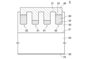
- FIG. 13(a) is a schematic plan view showing the configuration of a junction barrier Schottky diode 12 according to the twelfth embodiment of the present invention.
- FIG. 13(b) is a schematic cross-sectional view along line AA shown in FIG. 13(a).
- another peripheral trench 63 surrounding the peripheral trench 62 is provided in the drift layer 30, and the entire peripheral trench 63 is a p-type semiconductor. It differs from the junction barrier Schottky diode 1 according to the first embodiment in that it is filled with a material 80 .
- the outer trench 63 is provided independently of the outer trench 62 . Since other basic configurations are the same as those of the junction barrier Schottky diode 1 according to the first embodiment, the same elements are denoted by the same reference numerals, and overlapping descriptions are omitted. In FIG.
- the surface of the mesa region M that is in Schottky contact with the drift layer 30 is indicated by a broken line
- the surface of the mesa region M that is covered with the p-type semiconductor material 80 is indicated by a solid line.
- FIG. 14(a) is a schematic plan view showing the configuration of a junction barrier Schottky diode 13 according to the thirteenth embodiment of the present invention. Also, FIG. 14(b) is a schematic cross-sectional view taken along line AA shown in FIG. 14(a).
- the junction barrier Schottky diode 13 according to the thirteenth embodiment differs from the twelfth embodiment in that the width of the peripheral trench 63 is wider than the widths of the central trench 61 and the peripheral trench 62 . is different from the junction barrier Schottky diode 12 by Since other basic configurations are the same as those of the junction barrier Schottky diode 12 according to the twelfth embodiment, the same elements are denoted by the same reference numerals, and overlapping descriptions are omitted. By increasing the width of the outer trench 63 in this way, it is possible to relax the electric field concentrated near the bottom of the outer trench 63 when a reverse voltage is applied.
- FIG. 15(a) is a schematic plan view showing the configuration of a junction barrier Schottky diode 14 according to the fourteenth embodiment of the present invention.
- FIG. 15(b) is a schematic cross-sectional view along line AA shown in FIG. 15(a).
- the inner wall of the outer trench 63 is covered with an insulating film 70 made of HfO 2 or the like. It differs from the junction barrier Schottky diode 12 according to the twelfth embodiment in that it is embedded with an electrode 40 . Since other basic configurations are the same as those of the junction barrier Schottky diode 12 according to the twelfth embodiment, the same elements are denoted by the same reference numerals, and overlapping descriptions are omitted. Also in this embodiment, as in the twelfth embodiment, it is possible to further increase the reverse breakdown voltage.
- FIG. 16 is a schematic cross-sectional view showing the structure of a junction barrier Schottky diode 15 according to a fifteenth embodiment of the invention.
- the anode electrode 41 in Schottky contact with the drift layer 30 is made of a Cu single layer film or a Cu/Al laminated film. It is different from the junction barrier Schottky diode 2 according to the second embodiment in that the anode electrode 42 that is in ohmic contact with the semiconductor material 80 of the mold is made of Ni or the like. Since other basic configurations are the same as those of the junction barrier Schottky diode 2 according to the second embodiment, the same elements are denoted by the same reference numerals, and overlapping descriptions are omitted.
- the p-type semiconductor material 80 and the anode electrode 42 can be brought into ohmic contact. becomes possible, and the contact resistance is reduced.
- the p-type semiconductor material 80 is NiO
- Ni is used as the anode electrode 42
- both can be brought into ohmic contact.
- the p-type semiconductor material 80 is made of a material having a wider bandgap than NiO, it is preferable to use a metal such as Pt having a larger work function than Ni as the anode electrode 42 .
- Example 1> Assuming a simulation model of an embodiment having the same structure as the junction barrier Schottky diode 1 shown in FIG. .
- the dopant concentration of the semiconductor substrate 20 was set to 1 ⁇ 10 18 cm ⁇ 3 and the dopant concentration of the drift layer 30 was set to 3 ⁇ 10 16 cm ⁇ 3 .
- the thickness of the drift layer 30 was set to 7 ⁇ m.
- the depths of the central trench 61 and the peripheral trench 62 were both set to 3 ⁇ m.
- the widths of the central trench 61 and the peripheral trench 62 and the width of the upper surface 31 of the drift layer 30 (the width of the mesa region M) in the cross section shown in FIG. 1B are all set to 1.5 ⁇ m.
- the curvature radius of the curved surface 34 positioned between the flat bottom surface 32 and the side surface 33 of the central trench 61 and the outer peripheral trench 62 was set to 0.2 ⁇ m.
- NiO was used as the p-type semiconductor material 80 .
- the material of the anode electrode 40 was Ni, and the material of the cathode electrode 50 was a laminated film of Ti and Au.
- a simulation was performed using the depth T of the anode electrode 40 in contact with the side surfaces 33 of the central trench 61 and the peripheral trench 62 as a variable.
- junction barrier Schottky diode 20 semiconductor substrate 21 top surface 22 of semiconductor substrate back surface 30 drift layer 31 top surface of drift layer 32 bottom surface of trench 33 side surface 33a of trench inner side surface 33b inner side surface 33b of trench outer side surface 34 of trench curved surface 35 trench corners 40 to 42 anode electrode 50 cathode electrode 61 central trenches 62, 63 outer trenches 70, 71 insulating film 80 semiconductor material M mesa region
Landscapes
- Electrodes Of Semiconductors (AREA)
Priority Applications (3)
| Application Number | Priority Date | Filing Date | Title |
|---|---|---|---|
| DE112022005676.2T DE112022005676T5 (de) | 2021-11-29 | 2022-08-12 | Sperrschicht-schottky-diode |
| CN202280079132.0A CN118318310A (zh) | 2021-11-29 | 2022-08-12 | 结势垒肖特基二极管 |
| US18/676,107 US20240313130A1 (en) | 2021-11-29 | 2024-05-28 | Junction barrier schottky diode |
Applications Claiming Priority (2)
| Application Number | Priority Date | Filing Date | Title |
|---|---|---|---|
| JP2021193060A JP7770170B2 (ja) | 2021-11-29 | 2021-11-29 | ジャンクションバリアショットキーダイオード |
| JP2021-193060 | 2021-11-29 |
Related Child Applications (1)
| Application Number | Title | Priority Date | Filing Date |
|---|---|---|---|
| US18/676,107 Continuation US20240313130A1 (en) | 2021-11-29 | 2024-05-28 | Junction barrier schottky diode |
Publications (1)
| Publication Number | Publication Date |
|---|---|
| WO2023095396A1 true WO2023095396A1 (ja) | 2023-06-01 |
Family
ID=86539150
Family Applications (1)
| Application Number | Title | Priority Date | Filing Date |
|---|---|---|---|
| PCT/JP2022/030766 Ceased WO2023095396A1 (ja) | 2021-11-29 | 2022-08-12 | ジャンクションバリアショットキーダイオード |
Country Status (6)
| Country | Link |
|---|---|
| US (1) | US20240313130A1 (https=) |
| JP (1) | JP7770170B2 (https=) |
| CN (1) | CN118318310A (https=) |
| DE (1) | DE112022005676T5 (https=) |
| TW (1) | TWI827223B (https=) |
| WO (1) | WO2023095396A1 (https=) |
Cited By (1)
| Publication number | Priority date | Publication date | Assignee | Title |
|---|---|---|---|---|
| WO2025013328A1 (ja) * | 2023-07-13 | 2025-01-16 | 株式会社 東芝 | 半導体装置 |
Families Citing this family (3)
| Publication number | Priority date | Publication date | Assignee | Title |
|---|---|---|---|---|
| TWI901178B (zh) * | 2023-09-21 | 2025-10-11 | 日商Tdk股份有限公司 | 半導體裝置 |
| CN118841453A (zh) * | 2024-08-09 | 2024-10-25 | 乐山希尔电子股份有限公司 | 一种垂直型宽禁带肖特基功率二极管及其制备方法 |
| CN119451139A (zh) * | 2024-10-31 | 2025-02-14 | 中国电子科技集团公司第五十八研究所 | 一种沟槽型氧化镓异质结势垒肖特基二极管 |
Citations (6)
| Publication number | Priority date | Publication date | Assignee | Title |
|---|---|---|---|---|
| JP2008519448A (ja) * | 2004-11-08 | 2008-06-05 | ローベルト ボツシユ ゲゼルシヤフト ミツト ベシユレンクテル ハフツング | 半導体デバイスおよび半導体デバイスの製造方法 |
| CN102222701A (zh) * | 2011-06-23 | 2011-10-19 | 哈尔滨工程大学 | 一种沟槽结构肖特基器件 |
| JP2012124268A (ja) * | 2010-12-07 | 2012-06-28 | Nippon Inter Electronics Corp | 半導体装置 |
| JP2016178182A (ja) * | 2015-03-19 | 2016-10-06 | 新電元工業株式会社 | 半導体装置およびその製造方法 |
| JP2019041106A (ja) * | 2017-08-24 | 2019-03-14 | 株式会社Flosfia | 半導体装置 |
| CN110137268A (zh) * | 2019-06-21 | 2019-08-16 | 派恩杰半导体(杭州)有限公司 | 一种带有沟槽电极的高压二极管 |
Family Cites Families (8)
| Publication number | Priority date | Publication date | Assignee | Title |
|---|---|---|---|---|
| JP2009177028A (ja) * | 2008-01-25 | 2009-08-06 | Toshiba Corp | 半導体装置 |
| KR101220568B1 (ko) * | 2008-03-17 | 2013-01-21 | 미쓰비시덴키 가부시키가이샤 | 반도체 장치 |
| US8372738B2 (en) * | 2009-10-30 | 2013-02-12 | Alpha & Omega Semiconductor, Inc. | Method for manufacturing a gallium nitride based semiconductor device with improved termination scheme |
| JP6845397B2 (ja) * | 2016-04-28 | 2021-03-17 | 株式会社タムラ製作所 | トレンチmos型ショットキーダイオード |
| JP7037142B2 (ja) | 2017-08-10 | 2022-03-16 | 株式会社タムラ製作所 | ダイオード |
| JP7045008B2 (ja) * | 2017-10-26 | 2022-03-31 | Tdk株式会社 | ショットキーバリアダイオード |
| JP7371484B2 (ja) * | 2019-12-18 | 2023-10-31 | Tdk株式会社 | ショットキーバリアダイオード |
| JP7415537B2 (ja) * | 2019-12-18 | 2024-01-17 | Tdk株式会社 | ショットキーバリアダイオード |
-
2021
- 2021-11-29 JP JP2021193060A patent/JP7770170B2/ja active Active
-
2022
- 2022-08-12 WO PCT/JP2022/030766 patent/WO2023095396A1/ja not_active Ceased
- 2022-08-12 DE DE112022005676.2T patent/DE112022005676T5/de active Pending
- 2022-08-12 CN CN202280079132.0A patent/CN118318310A/zh active Pending
- 2022-08-30 TW TW111132598A patent/TWI827223B/zh active
-
2024
- 2024-05-28 US US18/676,107 patent/US20240313130A1/en active Pending
Patent Citations (6)
| Publication number | Priority date | Publication date | Assignee | Title |
|---|---|---|---|---|
| JP2008519448A (ja) * | 2004-11-08 | 2008-06-05 | ローベルト ボツシユ ゲゼルシヤフト ミツト ベシユレンクテル ハフツング | 半導体デバイスおよび半導体デバイスの製造方法 |
| JP2012124268A (ja) * | 2010-12-07 | 2012-06-28 | Nippon Inter Electronics Corp | 半導体装置 |
| CN102222701A (zh) * | 2011-06-23 | 2011-10-19 | 哈尔滨工程大学 | 一种沟槽结构肖特基器件 |
| JP2016178182A (ja) * | 2015-03-19 | 2016-10-06 | 新電元工業株式会社 | 半導体装置およびその製造方法 |
| JP2019041106A (ja) * | 2017-08-24 | 2019-03-14 | 株式会社Flosfia | 半導体装置 |
| CN110137268A (zh) * | 2019-06-21 | 2019-08-16 | 派恩杰半导体(杭州)有限公司 | 一种带有沟槽电极的高压二极管 |
Cited By (1)
| Publication number | Priority date | Publication date | Assignee | Title |
|---|---|---|---|---|
| WO2025013328A1 (ja) * | 2023-07-13 | 2025-01-16 | 株式会社 東芝 | 半導体装置 |
Also Published As
| Publication number | Publication date |
|---|---|
| CN118318310A (zh) | 2024-07-09 |
| DE112022005676T5 (de) | 2024-09-12 |
| TWI827223B (zh) | 2023-12-21 |
| JP2023079552A (ja) | 2023-06-08 |
| US20240313130A1 (en) | 2024-09-19 |
| TW202322405A (zh) | 2023-06-01 |
| JP7770170B2 (ja) | 2025-11-14 |
Similar Documents
| Publication | Publication Date | Title |
|---|---|---|
| US11626522B2 (en) | Schottky barrier diode | |
| TWI798402B (zh) | 肖特基能障二極體 | |
| US11621357B2 (en) | Schottky barrier diode | |
| US11908955B2 (en) | Schottky barrier diode | |
| US11557681B2 (en) | Schottky barrier diode | |
| JP7770170B2 (ja) | ジャンクションバリアショットキーダイオード | |
| US20240313129A1 (en) | Schottky barrier diode | |
| US11699766B2 (en) | Schottky barrier diode | |
| US20260006809A1 (en) | Junction barrier schottky diode | |
| US12520510B2 (en) | Schottky barrier diode | |
| US20260013157A1 (en) | Schottky barrier diode | |
| JP2023141101A (ja) | ジャンクションバリアショットキーダイオード |
Legal Events
| Date | Code | Title | Description |
|---|---|---|---|
| 121 | Ep: the epo has been informed by wipo that ep was designated in this application |
Ref document number: 22898181 Country of ref document: EP Kind code of ref document: A1 |
|
| WWE | Wipo information: entry into national phase |
Ref document number: 202280079132.0 Country of ref document: CN |
|
| 122 | Ep: pct application non-entry in european phase |
Ref document number: 22898181 Country of ref document: EP Kind code of ref document: A1 |