WO2023095199A1 - 量子デバイス、量子コンピュータ及び量子デバイスの製造方法 - Google Patents
量子デバイス、量子コンピュータ及び量子デバイスの製造方法 Download PDFInfo
- Publication number
- WO2023095199A1 WO2023095199A1 PCT/JP2021/042964 JP2021042964W WO2023095199A1 WO 2023095199 A1 WO2023095199 A1 WO 2023095199A1 JP 2021042964 W JP2021042964 W JP 2021042964W WO 2023095199 A1 WO2023095199 A1 WO 2023095199A1
- Authority
- WO
- WIPO (PCT)
- Prior art keywords
- layer
- topological insulator
- quantum device
- dimensional topological
- protective layer
- Prior art date
- Legal status (The legal status is an assumption and is not a legal conclusion. Google has not performed a legal analysis and makes no representation as to the accuracy of the status listed.)
- Ceased
Links
Images













Definitions
- the present disclosure relates to quantum devices, quantum computers, and methods of manufacturing quantum devices.
- An object of the present disclosure is to provide a quantum device, a quantum computer, and a method for manufacturing a quantum device that can easily stabilize characteristics.
- a substrate a two-dimensional topological insulator layer provided on the substrate, a first protective layer covering the two-dimensional topological insulator layer, and provided on the first protective layer a quantum device comprising: an opening exposing a side surface of the two-dimensional topological insulator layer; and a superconductor layer provided in the opening and in contact with the side surface of the two-dimensional topological insulator layer.
- the characteristics can be easily stabilized.
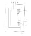
- FIG. 1 is a top view showing the quantum device according to the first embodiment.
- FIG. 2 is a cross-sectional view showing the quantum device according to the first embodiment.
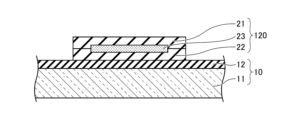
- FIG. 3 is a cross-sectional view (Part 1) showing the method of manufacturing the quantum device according to the first embodiment.
- FIG. 4 is a cross-sectional view (part 2) showing the method of manufacturing the quantum device according to the first embodiment.
- FIG. 5 is a cross-sectional view (No. 3) showing the method for manufacturing the quantum device according to the first embodiment.
- FIG. 6 is a cross-sectional view (No. 4) showing the method of manufacturing the quantum device according to the first embodiment.
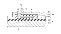
- FIG. 7 is a cross-sectional view (No. 5) showing the method for manufacturing the quantum device according to the first embodiment.
- FIG. 8 is a cross-sectional view (No. 6) showing the method for manufacturing the quantum device according to the first embodiment.
- FIG. 9 is a cross-sectional view (No. 7) showing the method for manufacturing the quantum device according to the first embodiment.
- FIG. 10 is a cross-sectional view (No. 8) showing the method of manufacturing the quantum device according to the first embodiment.
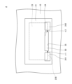
- FIG. 11 is a top view (part 1) showing the method of manufacturing the quantum device according to the first embodiment.
- 12 is a top view (part 2) showing the method for manufacturing the quantum device according to the first embodiment;
- FIG. FIG. 13 is a top view (part 3) showing the method of manufacturing the quantum device according to the first embodiment;
- FIG. 14 is a top view (No. 4) showing the method for manufacturing the quantum device according to the first embodiment.
- FIG. 15 is a top view (No. 5) showing the method of manufacturing the quantum device according to the first embodiment.
- 16 is a top view (No. 6) showing the method for manufacturing the quantum device according to the first embodiment;
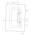
- FIG. FIG. 17 is a top view showing the quantum device according to the second embodiment.
- FIG. 18 is a top view (No. 1) showing the method of manufacturing the quantum device according to the second embodiment.
- FIG. 19 is a top view (Part 2) showing the method of manufacturing the quantum device according to the second embodiment.
- FIG. 20 is a top view (No. 3) showing the method of manufacturing the quantum device according to the second embodiment.
- FIG. 21 is a top view (No. 4) showing the method of manufacturing the quantum device according to the second embodiment.
- FIG. 22 is a top view (No. 5) showing the method of manufacturing the quantum device according to the first embodiment.
- 16 is a top view (No. 6) showing the method for manufacturing the quantum device according to the first embodiment;
- FIG. 17 is a top
- FIG. 24 is a cross-sectional view showing a quantum device according to a third embodiment
- FIG. 25 is a cross-sectional view (No. 1) showing the method of manufacturing the quantum device according to the third embodiment.
- FIG. 26 is a cross-sectional view (Part 2) showing the method of manufacturing the quantum device according to the third embodiment.
- FIG. 27 is a cross-sectional view (No. 3) showing the method of manufacturing the quantum device according to the third embodiment.
- FIG. 28 is a diagram showing a quantum computer according to the fifth embodiment.
- FIG. 1 is a top view showing the quantum device according to the first embodiment.
- FIG. 2 is a cross-sectional view showing the quantum device according to the first embodiment.
- FIG. 2 corresponds to a cross-sectional view taken along line II-II in FIG.
- Quantum device 1 includes, as shown in FIGS. , and the gate electrode 92 . Note that the gate insulating layer 91 and the gate electrode 92 are omitted in FIG.
- the substrate 10 has a Si substrate 11 and a Si oxide film 12 formed on the Si substrate 11 .
- Substrate 10 may be an insulating substrate.
- the laminate 120 has a first protective layer 21 , a second protective layer 22 and a two-dimensional topological insulator layer 23 .
- the two-dimensional topological insulator layer 23 is, for example, a single layer of 1T'-2 tungsten telluride (WTe 2 ).
- the two-dimensional topological insulator layer 23 may be a single layer of 1T'-2 tungsten selenide (WSe 2 ) or 1T'-2 molybdenum telluride (MoTe 2 ).
- the thickness of the two-dimensional topological insulator layer 23 is, for example, about 1 nm.
- the two-dimensional topological insulator layer 23 has an edge 23E.
- the first protective layer 21 and the second protective layer 22 contain, for example, hexagonal boron nitride (h-BN).
- the first protective layer 21 and the second protective layer 22 may be h-BN layers.
- An h-BN layer is an example of a layered material layer.
- the thicknesses of the first protective layer 21 and the second protective layer 22 are, for example, about 10 nm to 20 nm.
- the first protective layer 21 covers one surface (first surface) of the two-dimensional topological insulator layer 23, and the second protective layer 22 covers the other surface (second surface) of the two-dimensional topological insulator layer 23. cover.
- first protective layer 21 and the second protective layer 22 are in contact with each other outside the edge 23E of the two-dimensional topological insulator layer 23 over the entire circumference of the two-dimensional topological insulator layer 23 .
- the laminate 120 is provided on the substrate 10 with the two-dimensional topological insulator layer 23 on the substrate 10 side of the first protective layer 21 .
- a second protective layer 22 is in contact with the substrate 10 .
- An opening 25 is formed in the laminate 120 .
- the opening 25 penetrates the first protective layer 21 .
- the side surface of the two-dimensional topological insulator layer 23 is exposed through the opening 25 .
- a recess 24 forming an opening 25 is formed in the two-dimensional topological insulator layer 23 in plan view.
- the opening 25 may reach the second protective layer 22 , and the bottom surface of the opening 25 may be closer to the substrate 10 than the upper surface of the second protective layer 22 .
- Openings 26 and 27 are formed in the laminate 120 . Openings 26 and 27 penetrate first protective layer 21 . The openings 26 and 27 may reach the second protective layer 22 , and the bottom surfaces of the openings 26 and 27 may be closer to the substrate 10 than the upper surface of the second protective layer 22 .
- the opening 26 is formed along the edge 23E of the two-dimensional topological insulator layer 23 and away from the opening 25 to one side.
- the opening 27 is formed away from the opening 25 along the edge 23E of the two-dimensional topological insulator layer 23 on the other side.
- An opening 25 is located between the openings 26 and 27 . Openings 26 and 27 are spaced from edge 23E.
- the superconductor layer 30 is provided within the opening 25 .
- the superconductor layer 30 is in contact with the side surface of the two-dimensional topological insulator layer 23 , and the side surface of the two-dimensional topological insulator layer 23 exposed to the opening 25 is covered with the superconductor layer 30 .
- the superconductor layer 30 may protrude above the upper surface of the first protective layer 21 .
- the superconductor layer 30 is, for example, a tungsten (W) layer.
- the thickness of the superconductor layer 30 is, for example, about 10 nm to 30 nm.
- the magnetic layer 141 is provided inside the opening 26 .
- the magnetic layer 142 is provided inside the opening 27 .
- the magnetic layers 141 and 142 generate a magnetic field that reaches the two-dimensional topological insulator layer 23 .
- the magnetic layers 141 and 142 are separated from the edge 23E of the two-dimensional topological insulator layer 23 and are not in contact with the two-dimensional topological insulator layer 23 .
- the magnetic layers 141 and 142 are, for example, cobalt (Co) layers.
- a gate insulating layer 91 is provided on the substrate 10 so as to cover the laminate 120 and the superconductor layer 30 .
- Gate electrode 92 is provided on gate insulating layer 91 .
- the gate insulating layer 91 is, for example, a thin film layer of silicon nitride ( Si3N4 ), silicon dioxide ( SiO2 ), or hexagonal boron nitride.
- the gate electrode 92 is, for example, a gold (Au) electrode.
- the edge state of the two-dimensional topological insulator layer 23 forms an edge channel at the edge 23E.
- Majorana quasiparticles ⁇ 1 appear in the portion closer to the magnetic layer 141 than the superconductor layer 30, and Majorana quasiparticles ⁇ 2 appear in the portion closer to the magnetic layer 142 than the superconductor layer 30.
- the Majorana quasiparticle ⁇ 1 is constrained in the vicinity of the superconductor layer 30 by the influence of the magnetic field generated by the magnetic layer 141
- the Majorana quasiparticle ⁇ 2 is constrained in the vicinity of the superconductor layer 30 by the influence of the magnetic field generated by the magnetic layer 142. Constrained in the vicinity of layer 30 .
- the distance between the superconductor layer 30 and the magnetic layers 141 and 142 is, for example, about 50 nm to 500 nm.
- 3 to 10 are cross-sectional views showing the method of manufacturing the quantum device 1 according to the first embodiment.
- 11 to 16 are top views showing the method of manufacturing the quantum device 1 according to the first embodiment.
- a laminate 120 is formed.
- the two-dimensional topological insulator layer 23 is prepared in a non-oxidizing atmosphere such as an argon (Ar) atmosphere.
- the two-dimensional topological insulator layer 23 can be obtained, for example, by peeling a single layer of 1T'-WTe 2 from bulk WTe 2 .
- the first protective layer 21 is attached to one surface of the two-dimensional topological insulator layer 23, and the second protective layer 22 is attached to the other surface. paste.
- a laminate 120 is provided on the substrate 10 with the two-dimensional topological insulator layer 23 positioned closer to the substrate 10 than the first protective layer 21 is.
- the laminate 120 is provided on the substrate 10 such that the second protective layer 22 is in contact with the substrate 10 .
- the laminate 120 can be provided on the substrate 10 by, for example, a stamping method.
- the laminate 120 may be provided on the substrate 10 in the air. This is because the entirety of the two-dimensional topological insulator layer 23 is covered with the first protective layer 21 and the second protective layer 22, and oxidation of the two-dimensional topological insulator layer 23 is prevented.
- FIG. 4 corresponds to a cross-sectional view taken along line IV-IV in FIG.
- a sacrificial layer 81 covering the laminate 120 is formed on the substrate 10.
- the sacrificial layer 81 can be formed by vapor deposition, for example.
- the sacrificial layer 81 is, for example, an aluminum (Al) layer.
- the sacrificial layer 81 may be an Au layer.
- the thickness of the sacrificial layer 81 is preferably 20 nm or more, more preferably 30 nm or more.
- FIG. 5 corresponds to a cross-sectional view taken along line V-V in FIG.
- a protective layer 82 is formed on the sacrificial layer 81.
- FIG. As described below, apertures 25, 26 and 27 are formed using a focused ion beam (FIB).
- the protective layer 82 is provided above the portion intended to suppress damage due to FIB irradiation when forming the openings 25 , 26 and 27 .
- a protective layer 82 is formed around the areas where openings 25, 26 and 27 are to be formed, over the portions of two-dimensional topological insulator layer 23 that remain after openings 25, 26 and 27 are formed.
- the protective layer 82 is, for example, a platinum (Pt) layer.
- the thickness of the protective layer 82 is, for example, approximately 20 nm to 50 nm.
- the protective layer 82 can be formed using FIB, for example. If the output of the FIB when forming the protective layer 82 is about 5 V, the sacrificial layer 81 can suppress damage to the laminated body 120 .
- FIG. 6 corresponds to a cross-sectional view taken along line VI-VI in FIG.
- openings 25, 26 and 27 are formed in the laminate 120.
- FIG. Apertures 25, 26 and 27 can be formed, for example, using a FIB in vacuum.
- the opening 25 is formed to penetrate the first protective layer 21 and expose the side surface of the two-dimensional topological insulator layer 23 . That is, the opening 25 is formed by removing part of the two-dimensional topological insulator layer 23 . As a result, a portion of the edge 23E of the two-dimensional topological insulator layer 23 is moved to form a recess 24 that constitutes the opening 25 in the two-dimensional topological insulator layer 23 .
- the second protective layer 22 is exposed at the bottoms of the openings 25 , 26 and 27 .
- FIG. 7 corresponds to a cross-sectional view taken along line VII-VII in FIG.
- a superconductor layer 30 is formed in the opening 25.
- FIG. The superconductor layer 30 can be formed, for example, using FIB in vacuum.
- the formation of openings 25, 26 and 27 and the formation of superconductor layer 30 may be performed consecutively in the same apparatus without exposure to the atmosphere.
- the superconductor layer 30 is formed to have a thickness sufficient to cover at least the entire side surface exposed in the opening 25 of the two-dimensional topological insulator layer 23 .
- a magnetic layer 141 is formed in the opening 26 and a magnetic layer 142 is formed in the opening 27 .
- the magnetic layers 141 and 142 can be formed using FIB in vacuum, for example.
- FIG. 8 corresponds to a cross-sectional view taken along line VIII-VIII in FIG.
- the sacrificial layer 81 is removed. Along with the removal of the sacrificial layer 81, the protective layer 82 and the cutting residue 83 are also removed. If the sacrificial layer 81 is an Al layer, the sacrificial layer 81 can be removed using hydrochloric acid. If the sacrificial layer 81 is an Au layer, the sacrificial layer 81 can be removed using a solution containing iodine.
- FIG. 9 corresponds to a cross-sectional view taken along line IX-IX in FIG.
- a gate insulating layer 91 and a gate electrode 92 are formed.
- the gate insulating layer 91 can be formed, for example, by an atomic layer deposition (ALD) method.
- the gate electrode 92 can be formed, for example, by vapor deposition using a mask and lift-off by removal of the mask.
- the gate electrode 92 may be formed by deposition and subsequent etching.
- the quantum device 1 according to the first embodiment can be manufactured.
- the superconductor layer 30 is provided within the opening 25 and is in contact with the edge 23E of the two-dimensional topological insulator layer 23 . Therefore, it is easy to achieve a stable relationship among the two-dimensional topological insulator layer 23, the superconductor layer 30, and the magnetic layers 141 and 142 for expressing the Majorana quasiparticles ⁇ 1 and ⁇ 2.
- the openings 25, 26 and 27 are formed using FIB, the openings 25, 26 and 27 can be formed with high precision.
- the preparation of the laminate 120 and the processing from the formation of the opening 25 to the formation of the superconductor layer 30 are performed in a non-oxidizing atmosphere, the oxidation of the two-dimensional topological insulator layer 23 can be prevented. It can be easily suppressed, and fluctuations in properties due to oxidation can be suppressed.
- the protective layer 82 is formed before the openings 25, 26 and 27 are formed, damage to the laminate 120 during the formation of the openings 25, 26 and 27 can be suppressed.
- the shape of the two-dimensional topological insulator layer 23 may differ each time it is separated. According to the present embodiment, even if the shape of the two-dimensional topological insulator layer 23 changes each time the two-dimensional topological insulator layer 23 is peeled off, the superconductor layer 30 and the magnetic layers 141 and 142 are combined into the shape of the two-dimensional topological insulator layer 23 . can be placed appropriately according to
- FIG. 17 is a top view showing the quantum device according to the second embodiment. Note that the gate insulating layer 91 and the gate electrode 92 are omitted in FIG.
- the openings 26 and 27 are not formed in the laminate 120, and the magnetic layers 241 and 242 are provided instead of the magnetic layers 141 and 142. is provided.
- the magnetic layer 241 is provided on the first protective layer 21 along the edge 23E of the two-dimensional topological insulator layer 23, away from the superconductor layer 30 to one side.
- the magnetic layer 242 is provided on the first protective layer 21 along the edge 23E of the two-dimensional topological insulator layer 23 and away from the superconductor layer 30 on the other side.
- a superconductor layer 30 is located between the magnetic layers 241 and 242 .
- the magnetic layers 241 and 242 overlap the edge 23E of the two-dimensional topological insulator layer 23 in plan view.
- the magnetic layers 241 and 242 generate a magnetic field that reaches the two-dimensional topological insulator layer 23 .
- the magnetic layers 241 and 242 are not in contact with the two-dimensional topological insulator layer 23 .
- the magnetic layers 241 and 242 are Co layers, for example.
- the Majorana quasiparticle ⁇ 1 appears in the portion closer to the magnetic layer 141 than the superconductor layer 30, and the Majorana quasiparticle ⁇ 2 appears in the portion closer to the magnetic layer 142 than the superconductor layer 30.
- the Majorana quasiparticle ⁇ 1 is constrained in the vicinity of the superconductor layer 30 by the influence of the magnetic field generated by the magnetic layer 141
- the Majorana quasiparticle ⁇ 2 is constrained in the vicinity of the superconductor layer 30 by the influence of the magnetic field generated by the magnetic layer 142. Constrained in the vicinity of layer 30 .
- 18 to 23 are top views showing the method of manufacturing the quantum device 2 according to the second embodiment.
- the processes up to the step of providing the laminate 120 on the substrate 10 are performed (see FIGS. 4 and 11).
- magnetic layers 241 and 242 are formed on the first protective layer 21 .
- the magnetic layers 241 and 242 can be formed, for example, by vapor deposition using a mask and lift-off by removal of the mask.
- the magnetic layers 241 and 242 may be formed by film formation and subsequent etching.
- a sacrificial layer 81 is formed on the substrate 10 to cover the laminate 120 and the magnetic layers 241 and 242 .
- the sacrificial layer 81 is, for example, an Al layer or an Au layer.
- a protective layer 82 is formed on the sacrificial layer 81 .
- the positions of the magnetic layers 241 and 242 may be specified using a scanning ion microscope (SIM) or the like, and the magnetic layers 241 and 242 may be used as alignment marks.
- the protective layer 82 is provided above a portion to suppress damage caused by FIB irradiation when forming the opening 25 .
- a protective layer 82 is formed around the area where the opening 25 is to be formed, above the portion of the two-dimensional topological insulator layer 23 that remains after the opening 25 is formed.
- the protective layer 82 is, for example, a Pt layer.
- openings 25 are formed in the laminate 120 .
- a portion of the edge 23E of the two-dimensional topological insulator layer 23 is moved to form a recess 24 that constitutes the opening 25 in the two-dimensional topological insulator layer 23 .
- the second protective layer 22 is exposed at the bottom of the opening 25 .
- a cutting residue 83 may be generated around the opening 25 (see FIG. 7).
- a superconductor layer 30 is formed in the opening 25. Then, as shown in FIG. 22, a superconductor layer 30 is formed to have a thickness sufficient to cover at least the entire side surface exposed in the opening 25 of the two-dimensional topological insulator layer 23 . Material of the superconductor layer 30 may be deposited around the opening 25 during the formation of the superconductor layer 30 .
- the sacrificial layer 81 is removed. Along with the removal of the sacrificial layer 81, the protective layer 82 and the cutting residue 83 are also removed.
- a gate insulating layer 91 and a gate electrode 92 are formed (see FIG. 10).
- the quantum device 2 according to the second embodiment can be manufactured.
- the superconductor layer 30 is provided in the opening 25 and contacts the edge 23E of the two-dimensional topological insulator layer 23 . Therefore, it is easy to achieve a stable relationship among the two-dimensional topological insulator layer 23, the superconductor layer 30, and the magnetic layers 241 and 242 for expressing the Majorana quasiparticles ⁇ 1 and ⁇ 2.
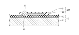
- FIG. 24 is a cross-sectional view showing a quantum device according to a third embodiment
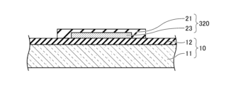
- a laminated body 320 is provided instead of the laminated body 120 .
- the laminate 320 has the first protective layer 21 and the two-dimensional topological insulator layer 23 and does not have the second protective layer 22 .
- the laminate 320 is provided on the substrate 10 with the two-dimensional topological insulator layer 23 on the substrate 10 side of the first protective layer 21 .
- a two-dimensional topological insulator layer 23 is in contact with the substrate 10 .
- the first protective layer 21 is also in contact with the substrate 10 outside the edge 23E of the two-dimensional topological insulator layer 23 over the entire circumference of the two-dimensional topological insulator layer 23 .
- the opening 25 may reach the substrate 10 , and the bottom surface of the opening 25 may be closer to the bottom surface of the substrate 10 than the top surface of the substrate 10 .
- the bottom surface of the opening 25 may be inside the Si oxide film 12 , inside the Si substrate 11 , or at the interface between the Si substrate 11 and the Si oxide film 12 .
- the bottom surface of the opening 25 may be on the top surface of the substrate 10 .
- the Majorana quasiparticle ⁇ 1 appears in the portion closer to the magnetic layer 141 than the superconductor layer 30, and the Majorana quasiparticle ⁇ 2 appears in the portion closer to the magnetic layer 142 than the superconductor layer 30. (See Figure 1).
- 25 to 27 are cross-sectional views showing the method of manufacturing the quantum device 3 according to the third embodiment.
- the two-dimensional topological insulator layer 23 is attached to the substrate 10 in a non-oxidizing atmosphere such as an Ar atmosphere, and the first protective layer 21 is formed on the two-dimensional topological insulator layer 23. paste. Thus, a laminate 320 is formed.
- a gate insulating layer 91 and a gate electrode 92 are formed in the same manner as in the first embodiment.
- the quantum device 3 according to the third embodiment can be manufactured.
- the superconductor layer 30 is provided in the opening 25 and contacts the edge 23E of the two-dimensional topological insulator layer 23 . Therefore, it is easy to achieve a stable relationship among the two-dimensional topological insulator layer 23, the superconductor layer 30, and the magnetic layers 141 and 142 for expressing the Majorana quasiparticles ⁇ 1 and ⁇ 2.
- the first surface of the two-dimensional topological insulator layer 23 is covered with the first protective layer 21 and the second surface is covered with the substrate 10. Oxidation of the insulator layer 23 can be easily suppressed, and variations in characteristics due to oxidation can be suppressed.
- FIG. 28 is a diagram showing a quantum computer according to the fifth embodiment.
- a quantum computer 4 according to the fourth embodiment has a general-purpose computer 401, a control unit 402, and a quantum device 403.
- the control unit 402 controls the quantum device 403 based on control signals from the general-purpose computer 401 .
- the quantum device 403 the quantum device according to any one of the first to third embodiments is used.
- the controller 402 and quantum device 403 are housed in a cryostat 404 .
- the quantum computer 4 can perform stable quantum operations.
- quantum device 4 quantum computer 10: substrate 21: first protective layer 22: second protective layer 23: two-dimensional topological insulator layer 23E: edge 24: recess 25, 26, 27: opening Part 30: Superconductor layer 81: Sacrificial layer 82: Protective layer 120, 320: Laminate 141, 142, 241, 242: Magnetic layer
Landscapes
- Superconductor Devices And Manufacturing Methods Thereof (AREA)
Priority Applications (2)
| Application Number | Priority Date | Filing Date | Title |
|---|---|---|---|
| JP2023563376A JP7729397B2 (ja) | 2021-11-24 | 2021-11-24 | 量子デバイス、量子コンピュータ及び量子デバイスの製造方法 |
| PCT/JP2021/042964 WO2023095199A1 (ja) | 2021-11-24 | 2021-11-24 | 量子デバイス、量子コンピュータ及び量子デバイスの製造方法 |
Applications Claiming Priority (1)
| Application Number | Priority Date | Filing Date | Title |
|---|---|---|---|
| PCT/JP2021/042964 WO2023095199A1 (ja) | 2021-11-24 | 2021-11-24 | 量子デバイス、量子コンピュータ及び量子デバイスの製造方法 |
Publications (1)
| Publication Number | Publication Date |
|---|---|
| WO2023095199A1 true WO2023095199A1 (ja) | 2023-06-01 |
Family
ID=86539046
Family Applications (1)
| Application Number | Title | Priority Date | Filing Date |
|---|---|---|---|
| PCT/JP2021/042964 Ceased WO2023095199A1 (ja) | 2021-11-24 | 2021-11-24 | 量子デバイス、量子コンピュータ及び量子デバイスの製造方法 |
Country Status (2)
| Country | Link |
|---|---|
| JP (1) | JP7729397B2 (https=) |
| WO (1) | WO2023095199A1 (https=) |
Citations (1)
| Publication number | Priority date | Publication date | Assignee | Title |
|---|---|---|---|---|
| US20200320420A1 (en) * | 2019-04-02 | 2020-10-08 | International Business Machines Corporation | Tunable superconducting resonator for quantum computing devices |
-
2021
- 2021-11-24 JP JP2023563376A patent/JP7729397B2/ja active Active
- 2021-11-24 WO PCT/JP2021/042964 patent/WO2023095199A1/ja not_active Ceased
Patent Citations (1)
| Publication number | Priority date | Publication date | Assignee | Title |
|---|---|---|---|---|
| US20200320420A1 (en) * | 2019-04-02 | 2020-10-08 | International Business Machines Corporation | Tunable superconducting resonator for quantum computing devices |
Non-Patent Citations (2)
| Title |
|---|
| HOSODA, MASAYUKI; DEACON, RUSSELL S.; YAMAGUCHI, TOMOHIRO; OKAZAKI, SHOTA; SASAGAWA, TAKAO; TANIGUCHI, TAKASHI; WATANABE, KENJI; K: "19a-Z31-5 Study of Contact Fabrication Process for Thin-Film WTe2 Devices", PROCEEDINGS OF THE 68TH JSAP SPRING MEETING; [ONLINE]; 16-19 MARCH 2021, vol. 68, 10 March 2021 (2021-03-10), JP, pages 15 - 104, XP009546644, DOI: 10.11470/jsapmeeting.2021.1.0_2903 * |
| RHODES DANIEL A., JINDAL APOORV, YUAN NOAH F. Q., JUNG YOUNGHUN, ANTONY ABHINANDAN, WANG HUA, KIM BUMHO, CHIU YU-CHE, TANIGUCHI TA: "Enhanced Superconductivity in Monolayer T d -MoTe 2", NANO LETTERS, vol. 21, no. 6, 24 March 2021 (2021-03-24), US , pages 2505 - 2511, XP093068945, ISSN: 1530-6984, DOI: 10.1021/acs.nanolett.0c04935 * |
Also Published As
| Publication number | Publication date |
|---|---|
| JPWO2023095199A1 (https=) | 2023-06-01 |
| JP7729397B2 (ja) | 2025-08-26 |
Similar Documents
| Publication | Publication Date | Title |
|---|---|---|
| US20090315122A1 (en) | Semiconductor device having ohmic recessed electrode | |
| TW200539277A (en) | A method for making a semiconductor device having a high-k gate dielectric layer and a metal gate electrode | |
| US20070170503A1 (en) | Composite substrate and method of fabricating the same | |
| JP2007273492A (ja) | 窒化物半導体装置およびその製造方法 | |
| JPS6129556B2 (https=) | ||
| JP6269276B2 (ja) | 半導体装置、半導体装置の製造方法 | |
| JP3664987B2 (ja) | 電子顕微鏡観察用試料の作成方法及び半導体装置の解析方法 | |
| JP2020017647A (ja) | 半導体装置の製造方法 | |
| JPS58500680A (ja) | 低抵抗合成金属導体を具えた半導体デバイスおよびその製造方法 | |
| JP2012069798A (ja) | 半導体装置の製造方法 | |
| US9842738B2 (en) | Method for manufacturing silicon carbide semiconductor device and silicon carbide semiconductor device | |
| WO2023095199A1 (ja) | 量子デバイス、量子コンピュータ及び量子デバイスの製造方法 | |
| US20250015169A1 (en) | Electronic device, quantum computer, and method for manufacturing electronic device | |
| JP2017152643A (ja) | 電子装置およびその製造方法 | |
| EP0696053A1 (fr) | Procédé de réalisation d'un transistor à effet de champ à canal creusé | |
| JP6369366B2 (ja) | 半導体装置の製造方法 | |
| JPS5832513B2 (ja) | 電界効果トランジスタの製造方法 | |
| JP7750757B2 (ja) | タングステンの貫通加工品を作製するためのタングステンブランクス、及びタングステンブランクスを用いたタングステン貫通加工品の製造方法 | |
| JP2004069628A (ja) | インライン検査試料作製方法 | |
| JPS6352473A (ja) | 化合物半導体装置 | |
| JPS62204576A (ja) | 縦型トランジスタの製造方法 | |
| JPH11260701A (ja) | 電子ビーム露光の位置合わせマーク | |
| CN105448694B (zh) | 半导体装置及其制造方法 | |
| JP2008244056A (ja) | 炭化珪素半導体装置の製造方法 | |
| JPS5842631B2 (ja) | 接合ゲ−ト型電界効果トランジスタの製造方法 |
Legal Events
| Date | Code | Title | Description |
|---|---|---|---|
| ENP | Entry into the national phase |
Ref document number: 2023563376 Country of ref document: JP Kind code of ref document: A |
|
| NENP | Non-entry into the national phase |
Ref country code: DE |
|
| 122 | Ep: pct application non-entry in european phase |
Ref document number: 21965573 Country of ref document: EP Kind code of ref document: A1 |