WO2023090349A1 - ジャイロセンサ素子 - Google Patents
ジャイロセンサ素子 Download PDFInfo
- Publication number
- WO2023090349A1 WO2023090349A1 PCT/JP2022/042514 JP2022042514W WO2023090349A1 WO 2023090349 A1 WO2023090349 A1 WO 2023090349A1 JP 2022042514 W JP2022042514 W JP 2022042514W WO 2023090349 A1 WO2023090349 A1 WO 2023090349A1
- Authority
- WO
- WIPO (PCT)
- Prior art keywords
- detection
- base
- sensor element
- gyro sensor
- arm
- Prior art date
Links
Images


Classifications
-
- G—PHYSICS
- G01—MEASURING; TESTING
- G01C—MEASURING DISTANCES, LEVELS OR BEARINGS; SURVEYING; NAVIGATION; GYROSCOPIC INSTRUMENTS; PHOTOGRAMMETRY OR VIDEOGRAMMETRY
- G01C19/00—Gyroscopes; Turn-sensitive devices using vibrating masses; Turn-sensitive devices without moving masses; Measuring angular rate using gyroscopic effects
- G01C19/56—Turn-sensitive devices using vibrating masses, e.g. vibratory angular rate sensors based on Coriolis forces
- G01C19/5607—Turn-sensitive devices using vibrating masses, e.g. vibratory angular rate sensors based on Coriolis forces using vibrating tuning forks
- G01C19/5621—Turn-sensitive devices using vibrating masses, e.g. vibratory angular rate sensors based on Coriolis forces using vibrating tuning forks the devices involving a micromechanical structure
Definitions
- the present disclosure relates to a gyro sensor element used in a gyro sensor.
- a piezoelectric vibration type sensor is known as a conventional technology (Patent Document 1).
- the piezoelectric body is excited by applying an AC voltage to the piezoelectric body.
- a Coriolis force is generated in a direction perpendicular to the excitation direction in accordance with the rotational speed (angular velocity).
- the angular velocity of the piezoelectric body can be detected by detecting an electrical signal generated according to the deformation of the piezoelectric body due to such Coriolis force.
- the gyro sensor of Patent Document 1 detects a signal generated by deformation of a piezoelectric body in the X-axis direction or the Z-axis direction of an orthogonal coordinate system XYZ.
- a gyro sensor element includes a first base extending in a first direction, a pair of first driving arms extending in a second direction intersecting the first direction, and extending from the first base. and a first detection arm positioned between the pair of first drive arms, wherein a region of the first base portion continuous with the base end of the first detection arm extends in the second direction. It has a groove.
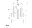
- FIG. 1 is a plan view showing a gyro sensor element according to Embodiment 1 of the present disclosure
- FIG. FIG. 2 is a cross-sectional view taken along line IA shown in FIG. 1
- FIG. 2 is a cross-sectional view taken along line IA shown in FIG. 1
- FIG. 2 is a cross-sectional view taken along line IB shown in FIG. 1
- FIG. 2 is a cross-sectional view taken along the line IC shown in FIG. 1
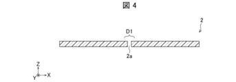
- FIG. 4 is a plan view showing a gyro sensor element according to another aspect of the present disclosure
- FIG. 3 is a diagram showing an example of a wiring pattern of a gyro sensor element
- 9 is a diagram showing an example of a wiring pattern of a gyro sensor element, and is a perspective view of the back surface of the gyro sensor element of FIG. 8 as seen from above.
- FIG. FIG. 2 is a cross-sectional view taken along the line IC shown in FIG. 1;
- FIG. 5 is a plan view showing a gyro sensor element according to Embodiment 2 of the present disclosure;
- FIG. 11 is a plan view showing a gyro sensor element according to Embodiment 3 of the present disclosure;
- FIG. 1 is a plan view showing a gyro sensor element 1 according to this embodiment.
- illustration of the conductive layer provided on the upper surface of the gyro sensor element 1 is basically omitted.
- the X-axis direction shown in FIG. 1 is called the first direction
- the Y-axis direction is called the second direction.
- the "upper surface” or “front surface” refers to the positive direction of the Z axis in FIG. 1, that is, the surface shown in FIG. It refers to the negative direction, ie the surface behind the surface shown in FIG.
- the gyro sensor element 1 may be integrally formed as a whole.
- the gyro sensor element 1 may be monocrystalline or polycrystalline.
- the base material of the gyro sensor element 1 may be selected as appropriate, such as crystal (SiO 2 ), LiTaO 3 , LiNbO 3 , PZT, or silicon.
- the gyro sensor element 1 may have, for example, a constant overall thickness (in the Z-axis direction).
- a gyro sensor element 1 is a sensor element used for a gyro sensor (not shown).
- the gyro sensor element 1 is made of a piezoelectric material, and includes a first base portion 2, a pair of first drive arms 3, a first detection arm 4, and a mounting portion 5, as shown in FIG. there is
- the pair of first drive arms 3 are excited in phases opposite to each other in the X-axis direction as indicated by an arrow C1 by applying an AC voltage. Being excited in phases opposite to each other means that the pair of first drive arms 3 vibrate so as to approach and separate from each other.
- the Coriolis force causes the first drive arm 3 to vibrate in the Y-axis direction as indicated by the arrow C2.
- the vibration of the first drive arm 3 is transmitted to the first detection arm 4 via the first base 2, and the first detection arm 4 performs bending vibration in the direction of the arrow C3 in the X-axis direction.
- a charge signal (for example, voltage) generated by the piezoelectric effect due to bending vibration of the first detection arm 4 is detected by a detection electrode, which will be described later, and the angular velocity is calculated from the detected voltage.
- the greater the angular velocity the greater the magnitude of the detected voltage. Further, even when detecting the same angular velocity, the larger the bending change of the first detection arm 4, the larger the voltage value obtained, so the angular velocity detection sensitivity of the gyro sensor becomes higher.
- the first base 2 supports a first drive arm 3 and a first detection arm 4 .
- the first base portion 2 extends in the first direction, and both ends thereof are supported by mounting portions 5 .
- FIG. 2 is a diagram showing the structure of the first base 2, and is a cross-sectional view taken along line IA shown in FIG.
- the first base portion 2 has a first groove portion 2a extending in the second direction in a region (region D1 shown in FIG. 1) continuous with the base end of the first detection arm 4. are doing.
- the depth of the first groove portion 2a in the Z-axis direction is not particularly limited.
- the first groove portion 2a may extend in the second direction from the base end of the first detection arm 4, which will be described later, to the distal end portion on the opposite side.
- the first base portion 2 Since the first base portion 2 has the first groove portion 2a in this way, a part of the region D1 of the first base portion 2 becomes thin, and the first base portion 2 becomes easy to bend. As the first base portion 2 bends, the first detection arm 4 tends to bend. According to this, the detection sensitivity of the gyro sensor element 1 can be improved.
- FIG. 2 is a cross-sectional view taken along line IA shown in FIG.
- the first groove portion 2a may be provided only on one surface (upper surface or lower surface) of the first base portion 2 as shown in FIG. 2, but is not limited to this. Another aspect of the first groove portion 2a will be illustrated.
- FIGS. 3 and 4 are diagrams showing the structure of the first base portion 2, respectively, and are sectional views taken along the line IA shown in FIG.
- the first base portion 2 has a first groove portion 2 a on the upper surface of the first base portion 2 and a first groove portion 2 b on the lower surface of the first base portion 2 .
- the thickness of the part of the region D1 of the first base 2 becomes thinner than the thickness of the part of the region D1 of the first base 2 shown in FIG. becomes easy to bend.
- the first detection arm 4 tends to bend.
- the first base portion 2 has a first groove portion 2a of a penetrating opening, that is, a first slit 2a.
- the groove portion of the through opening will also be referred to as a slit.
- the width of the first slit 2a may be the same from the top to the bottom of the first base 2, or may be different.
- the first slit 2a can be regarded as a form in which the bottom of the first groove 2a is removed, but only a part of the bottom of the first groove 2a is removed and a part is opened. good too.
- the first drive arm 3 is a portion that is excited by application of an AC voltage (electric field).
- the first drive arm 3 extends in the second direction from the first base 2 and has a free end.
- the first drive arm 3 can be flexurally deformed like a cantilever beam.
- the pair of first drive arms 3 are arranged in parallel with each other in the first direction, spaced apart from each other.
- FIG. 5 is a diagram showing the structure of the first driving arm 3, and is a cross-sectional view taken along line IB shown in FIG.
- the first drive arm 3 consists of two arms 3b separated by a slit 3a.
- the arm portion 3b has recesses extending in the second direction on both sides (upper surface and lower surface) in the Z-axis direction from the portion connected to the first base portion 2 to the end opposite to the first base portion 2.
- 3c second recess).
- the first drive arm 3 applies a voltage to the outer side surface of the first drive arm 3 (more specifically, the arm portion 3b) and the side surface on the side of the slit 3a.
- a first drive electrode 3d may be provided for this purpose.
- each recess 3c of the first drive arm 3 may be provided with a second drive electrode 3e to which a potential opposite to that of the first drive electrode 3d is applied.
- the other first drive arm 3 of the pair of first drive arms 3 is arranged such that the first drive electrode 3d and the second drive electrode 3e are located in the same position as one of the first drive arms 3. The opposite of the drive arm 3 may be used.
- the first drive arm 3 is provided with the second drive electrodes 3e on the outer side surface and the side surface on the side of the slit 3a, and the recesses 3c of the first drive arm 3 are provided with the first drive electrodes 3d. good too.
- the first detection arm 4 vibrates in the first direction due to the Coriolis force.
- the first detection arm 4 is provided with a first detection electrode 4g, a second detection electrode 4h, a first detection electrode 4j, and a second detection electrode 4k, which will be described later.
- a voltage generated by the piezoelectric effect resulting from the deflection in the first direction is measured by each sensing electrode.
- the first detection arm 4 may extend from the first base 2 in the second direction, as shown in FIG. In FIG. 1, as an example, the first detection arm 4 extends in the same second direction as the first drive arm 3 and is positioned between the pair of first drive arms 3, but is not limited to this.
- the first detection arm 4 may extend in the opposite direction to the direction in which the pair of first drive arms 3 extends, that is, in the negative direction of the Y-axis. Also, the first detection arm 4 may be positioned between the pair of first drive arms 3 when extending in the same second direction as the first drive arms 3 .
- the first detection arm 4 may be defined by a first groove 2a that is a bottomed groove extending from the first base 2, and the first detection arm 4 is defined by the first detection arm defined by the first groove 2a. A portion 4d and a second detection portion 4e may be provided. According to this, the first detection arm 4 has a thin portion, and the first detection arm 4 is easily bent.
- FIG. 6 is a diagram showing the configuration of the first detection arm 4, and is a cross-sectional view taken along the line IC shown in FIG.
- the first detection arm 4 has a slit 4c formed continuously with the slit 2a formed in the first base 2.
- the slit 4c may be a through opening slit.
- the slit 4c may extend from the first base portion 2 to the end opposite to the first base portion 2 .
- one slit is formed by the first slit 2a and the slit 4c.
- the first detection arm 4 may be composed of a first detection section 4d and a second detection section 4e separated by a slit 4c.
- the first detection portion 4d and the second detection portion 4e are arranged in the second direction on both sides in the Z-axis direction from the point where they are connected to the first base portion 2 to the end opposite to the first base portion 2. It may have a concave portion 4f and a concave portion 4m (first concave portion) extending inward.
- the ends of the first detection portion 4d and the second detection portion 4e may be connected to the first weight 4a, which is one weight.
- the first detection unit 4d has first detection electrodes 4g for detecting voltage generated by the piezoelectric effect on the side surface on the slit 4c side and the outer side surface, and the side surface of the recess 4f has a potential opposite to that of the first detection electrode 4g.
- a second detection electrode 4h for detecting the may be provided.
- the second detection part 4e includes first detection electrodes 4j for detecting the same voltage as the first detection electrodes 4g on the side surface on the slit 4c side and the outer side surface, and the first detection electrodes 4j on the side surfaces of the recess 4m. and a second detection electrode 4k for detecting a potential opposite to that of the second detection electrode 4k.
- the detection electrodes on the slit 4c side and the outer side of the first detection section 4d and the detection electrodes on the slit 4c side and the outer side of the second detection section 4e detect the same potential.
- the detection electrode on the side surface of the concave portion 4f of the first detection portion 4d and the detection electrode on the side surface of the concave portion 4m of the second detection portion 4e detect the same potential.
- the first base 2 extending in the second direction is provided in the region (region D1 shown in FIG. 1) continuous with the base end of the first detection arm 4 . It has a groove portion 2a (first slit). This makes it easier for the first base portion 2 to bend, so that the first detection arm 4 is easier to bend. As a result, in the gyro sensor element 1, the amplitude of vibration of the first detection arm 4 becomes larger than that of the conventional gyro sensor element, and has high detection sensitivity.
- the gyro sensor element 1 includes a first detection portion 4d and a second detection portion 4e separated by a slit 4c through which the first detection arm 4 passes. 4a.
- the first detection arm 4 has a structure in which the positions corresponding to each other change as the first detection portion 4d and the second detection portion 4e bend, so that the amplitude of vibration of the first detection arm 4 increases. .
- the detection sensitivity of the gyro sensor element 1 can be improved.
- the first detection portion 4d and the second detection portion 4e have a recess 4f and a recess 4m extending in the second direction, respectively.
- a second detection electrode 4h and a second detection electrode 4k) are provided.
- the first detection arm 4 includes a first detection electrode (that is, a first detection electrode 4g and a first detection electrode 4j) and a second detection electrode having opposite positive and negative potentials. Electrodes (ie, second detection electrode 4h and second detection electrode 4k) are provided. As a result, two potentials can be detected by the first detection arm 4, and detection sensitivity can be improved. Moreover, by covering each surface of the first detection arm 4 with electrodes, the rigidity of the first detection arm 4 can be increased.
- the first drive arm 3 extends in the second direction from the portion where the first drive arm 3 is connected to the first base portion 2 to the end opposite to the first base portion 2 (the second drive arm 3c). 2 recesses), and a first driving electrode 3d is provided on the outer side surface of the first driving arm 3 and the inner side surface of the recess 3c.
- the area for installing the driving electrodes can be made larger than that of the driving arm having no concave portion, and the electric field effect is strengthened, so that the driving arm can be vibrated more.
- the mounting portion 5 supports both ends of the first base portion 2 in the first direction. Further, the mounting portion 5 may be a portion that is fixed to, for example, a housing when the gyro sensor element 1 is mounted.
- the shape of the mounting portion 5 is not particularly limited, and it may be a frame upper member surrounding the four arms of the gyro sensor element 1 .
- the gyro sensor element 1 is basically composed of the first base portion 2, the pair of first drive arms 3, and the first detection arm 4 having the first detection portion 4d and the second detection portion 4e.
- one gyro sensor element may be provided with another unit of the above configuration.
- FIG. 7 is a plan view showing the gyro sensor element 1C.
- the gyro sensor element 1C may further include the following configurations (1) to (3) in addition to the configuration of the gyro sensor element 1.
- FIG. (1) A second base portion 12 arranged parallel to the first base portion 2 .
- (2) A pair of second drive arms 13 extending from the second base 12 in the second direction opposite to the direction in which the first drive arms 3 extend from the first base 2 .
- a second detection arm 14 extending from the second base 12 in the second direction opposite to the direction in which the first driving arm 3 extends from the first base 2 .
- a region D2 of the second base portion 12 of the gyro sensor element 1C, which is continuous with the base end of the second detection arm 14, may have a second groove portion 12a extending in the second direction.
- the second detection arm 14 may have a second groove 14c formed continuously with the second groove 12a. That is, the second groove portion 12a may extend in the second direction from the proximal end of the second detection arm 14 to the distal end on the opposite side. Further, the second groove portion 12a may be a through-opening second slit 12a, and the second groove portion 14c may be a through-opening second slit 14c.
- the second detection arm 14 of the gyro sensor element 1C may include a third detection portion 14d and a fourth detection portion 14e separated by a second groove portion 14c. That is, the third detection section 14d and the fourth detection section 14e separated by the second slit 14c may be provided. Further, the third detection section 14d may be located at the same position as the first detection section in the first direction, and the fourth detection section 14e may be located at the same position as the second detection section in the first direction.
- the third detection portion 14d and the fourth detection portion 14e are arranged in the second direction on both sides in the Z-axis direction from the point where they are connected to the second base portion 12 to the end opposite to the second base portion 12. You may have the recessed part extended to. Further, the distal ends of the third detecting portion 14d and the fourth detecting portion 14e may be connected to a second weight located at the end portion of the second detection arm 14 opposite to the proximal end thereof.
- the second drive arm 13 and the second detection arm 14 of the gyro sensor element 1C may each have an electrode.
- the pair of second drive arms 13 of the gyro sensor element 1C may be provided with first drive electrodes 3d and second drive electrodes 3e, like the pair of first drive arms 3.
- the second detection arm 14 of the gyro sensor element 1C may include first detection electrodes 4g and 4j and second detection electrodes 4h and 4k.
- the arrangement of the positive and negative electrodes of each detection electrode of the second detection arm 14 may be reverse to the arrangement of each detection electrode of the first detection arm 4 . That is, the concave portions of the third detecting portion 14d and the fourth detecting portion 14e are provided with the first detecting electrodes 4g and 4j, and the side surfaces of the third detecting portion 14d and the fourth detecting portion 14e on the side of the second slit 14c and the outer side surfaces thereof are provided with electrodes 4g and 4j. Second detection electrodes 4h and 4k may be provided.
- the gyro sensor element 1C has two structures of the gyro sensor element 1 shown in FIG. 1, one of which is inverted in the second direction. According to this, since the number of detection units included in the gyro sensor element 1 ⁇ /b>C is increased, the detection sensitivity is improved more than that of the gyro sensor element 1 ⁇ /b>C.
- FIG. 8 is a diagram showing an example of a wiring pattern on the surface of the gyro sensor element 1C, ie, the same surface as the plan view shown in FIG.
- FIG. 9 is a diagram showing an example of a wiring pattern on the back surface of the gyro sensor element 1C, and is a view of the back surface seen through from the front side.
- the wiring shown in each drawing also serves as an electrode.
- first drive arm 3A one of the pair of first drive arms 3 is called a first drive arm 3A
- first drive arm 3B one of the pair of second drive arms 13 is called a second drive arm.
- 13A and the other is called a second drive arm 13B.
- the gyro sensor element 1C may have a first wiring 420 connected to the first detection electrode.
- the first wiring 420 in FIG. 8 may be connected to the first detection electrodes 4g arranged on the slit 4c side and outer side surfaces of the first detection portion 4d.
- the first wiring 420 may be connected to the first detection electrodes 4j arranged on the slit 4c side and outer side surfaces of the second detection portion 4e.
- the first wiring 420 may be connected in the second detection arm 14 to the first detection electrodes arranged on the side surfaces of the recesses of the third detection section 14d and the fourth detection section 14e.
- the first wiring 420 may be connected to the back surface via a connecting portion 410U integrally provided from the front surface to the side surface of the first detection arm 4 .
- the connecting portion 410L is connected to the connecting portion 410U on the front surface.
- the first wiring 420 may be connected to the first detection electrodes 4g and 4j of the first detection arm 4 and the second detection arm 14, like the wiring pattern on the front surface.
- the gyro sensor element 1C may have a second wiring 410 connected to the second detection electrode.
- the second wiring 410 on the front surface of FIG. It is wiring connected to the detection electrode 4k.
- the second wiring 410 is connected to the second detection electrodes arranged on the second slit 14c side surface and the outer side surface of the third detection unit 14d, and to the second slit 14c side surface and the outer side surface of the fourth detection unit 14e. It may be connected to the arranged second detection electrode.
- the second wiring 410 is connected to the back surface via a connecting portion 410U integrally provided from the front surface to the side surface of the second detection arm 14 .
- the connecting portion 410L is connected to the connecting portion 410U on the front surface.
- the second wiring 410 may be connected to the second detection electrodes 4h and 4k of the first detection arm 4 and the second detection arm 14, like the wiring pattern on the front surface.
- the first wiring 420 and the second wiring 410 may be installed along the first base 2 and the second base 12 as a pair. According to this, the gyro sensor element 1C can efficiently detect potentials without generating excess charges, as compared with the case where the wires of the electrodes for detecting opposite potentials are arranged in different directions. Therefore, a gyro sensor element 1C with high detection sensitivity can be obtained.
- the gyro sensor element 1C corresponds to the third wiring 310 and the third wiring 320 connected to the driving electrodes (first driving electrode 3d, second driving electrode 3e).
- the third wiring 310 on the surface of FIG. 8 may be connected to the first driving electrode 3d arranged on the outer side surface of the first driving arm 3A and the side surface on the side of the slit 3a. Also, the third wiring 310 may be connected to the first drive electrode 3d arranged in the recess 3c of the first drive arm 3B. The third wiring 310 is further connected to the first driving electrode 3d arranged on the outer side surface of the second driving arm 13A and the side surface on the side of the slit 13a, and the second driving electrode 3d arranged in the concave portion of the second driving arm 13B. It may be connected to one drive electrode 3d.
- the third wiring 310 may be routed along the mounting portion 5 and connected to the rear surface via a connection portion 311U integrally provided from the front surface to the side surface of the mounting portion 5 .
- the connecting portion 311L may be connected to the connecting portion 311U on the front surface.
- the third wiring 310 may be connected to the first driving electrodes of the first driving arm 3 and the second driving arm 13, like the wiring pattern on the front surface.
- the third wiring 320 on the surface of FIG. 8 may be connected to the second drive electrode 3e to which the potential opposite to that of the first drive electrode 3d is applied.
- the third wiring 320 includes the second drive electrode 3e arranged in the recess 3c of the first drive arm 3A, the second drive electrode 3e arranged on the outer side surface of the first drive arm 3B, and the side surface on the side of the slit 3a. It may be connected to the electrode 3e.
- the third wiring 320 further includes a second drive electrode 3e arranged in the recess of the second drive arm 13A, a second drive electrode 3e arranged on the outer side surface of the second drive arm 13B, and a side surface on the side of the slit 13a. may be connected to the electrode 3e.
- the third wiring 320 may be wired along the mounting portion 5 on the front surface and connected to the rear surface via a connecting portion 321U integrally provided from the front surface to the side surface of the first driving arm 3A.
- the connecting portion 321L may be connected to the connecting portion 321U on the front surface.
- the third wiring 320 may be connected to the second driving electrodes 3e of the first driving arm 3 and the second driving arm 13, like the wiring pattern on the front surface.
- the gyro sensor element 1C may have a ground between the wiring connected to the detection electrodes and the wiring connected to the drive electrodes. That is, as shown in FIG. 9, the gyro sensor element 1C may have the ground 500 between the first wiring 420 and the second wiring 410 and the third wiring 310 and the third wiring 320 . According to this, the gyro sensor element 1C is connected to the wiring connected to the first detection electrodes 4g, 4j and the second detection electrodes 4h, 4k, and the first drive electrode 3d and the second drive electrode 3e. It is possible to reduce noise interference between the wiring and the wiring.
- the gyro sensor element 1 of the present disclosure may be formed by etching. At this time, convex portions may occur due to the influence of the crystal orientation of the quartz crystal that is the base material.
- the gyro sensor element 1 may have a convex portion on one of the surfaces of the base material of the first detection arm 4, the surface on the positive side and the surface on the negative side in the first direction.
- FIG. 10 is a diagram showing the first detection arm 4, and is a cross-sectional view taken along line 1-C shown in FIG.
- the first detection arm 4 has a convex portion 11 on the positive surface in the first direction of the first detection portion 4d and the second detection portion 4e.
- the convex portion 11 is indicated by hatching different from that of the first detection portion 4d and the second detection portion 4e for ease of explanation. be.
- FIG. 11 is a plan view showing the gyro sensor element 1D in this embodiment.
- a gyro sensor element 1D like the gyro sensor element 1C described above, has two structures of the gyro sensor element 1, one of which is inverted in the second direction. are the same.
- the gyro sensor element 1D is different from the gyro sensor element 1C in that the regions that are continuous with the base end of each detecting portion that is inverted in the second direction are connected by a bridging region.
- the first detection section 4d and the third detection section 14d may be connected by a first bridging region 21 in areas that are continuous with their base ends.
- the second bridging region 22 may connect the regions of the second detection portion 4e and the fourth detection portion 14e that are continuous with the respective proximal ends.
- the bridging region 21 and the bridging region 22 may be partitioned via a third groove portion 23 that is continuous with the first groove portion 4c and the second groove portion 14c.
- the first groove portion 4c may be the first slit 4c of the through opening
- the second groove portion 14c may be the second slit 14c of the through opening
- the third groove portion 23 may be the second slit 14c of the through opening. It may be 3 slits. That is, the first slit 4c and the second slit 14c may form an integral slit.
- the gyro sensor element 1D may include a bridging area 21 and a bridging area 22 that connect the detection units extending in the positive and negative directions of the second direction, and the two bridging areas may be partitioned or separated.
- each detecting portion can be easily bent, and the rigidity of the first detecting arm 4 and the second detecting arm 14 can be increased.
- the mounting portion 5 supports both ends of the first base portion 2 in the first direction without bending the first base portion 2 .
- both ends of the first base portion 2 ⁇ /b>C may be bent in the second direction and further bent in the first direction to be connected to the mounting portion 5 .
- FIG. 12 is a plan view showing a gyro sensor element 1B in this modified example. As shown in FIG. 12 , both ends of the first base portion 2 ⁇ /b>C are bent in the positive direction in the second direction, further bent in the first direction toward the mounting portion 5 , and connected to the mounting portion 5 . In FIG. 12, the bending angle is shown as a right angle, but the bending angle is not limited to this.
- both ends of the first base portion 2C are bent in the second direction and are further bent in the first direction to be connected to the mounting portion 5, so that the first base portion 2C is easily bent, As the first base portion 2C is curved, the first detection arm 4 is easily bent.
Abstract
本開示の一態様のジャイロセンサ素子は、第1方向に延伸した第1基部と、第1基部から、前記第1方向に交わる第2方向に延伸した一対の第1駆動腕と、第1基部から延伸した第1検出腕と、を備え、第1基部の第1検出腕の基端と連続する領域は、前記第2方向に延伸した第1溝部を有する。
Description
本開示は、ジャイロセンサに用いられるジャイロセンサ素子に関する。
ジャイロセンサとして、圧電振動式のセンサが従来技術として知られている(特許文献1)。このセンサは、圧電体に交流電圧が印加されることにより圧電体が励振する。励振されている圧電体に回転の動きが加わると、回転速度(角速度)に応じて、励振方向と直交する方向にコリオリの力が生じる。このようなコリオリの力に起因する圧電体の変形に応じて生じる電気信号を検出することにより、圧電体の角速度を検出することができる。特許文献1のジャイロセンサは、直交座標系XYZのX軸方向またはZ軸方向における圧電体の変形より生じる信号を検出する。
本開示の一態様に係るジャイロセンサ素子は、第1方向に延伸した第1基部と、前記第1方向に交わる第2方向に延伸した一対の第1駆動腕と、前記第1基部から延伸し、前記一対の第1駆動腕の間に位置した第1検出腕と、を備え、前記第1基部の前記第1検出腕の基端と連続する領域は、前記第2方向に延伸した第1溝部を有する。
<実施形態1>
以下、本開示の一実施形態について、詳細に説明する。図1は、本実施形態におけるジャイロセンサ素子1を示す平面図である。図1では、ジャイロセンサ素子1の上面に設けられる導電層の図示は基本的に省略されている。以上の説明では、図1に示すX軸方向を第1方向と呼称し、Y軸方向を第2方向と呼称して説明する。本明細書中で「上面」、または「表面」は、図1におけるZ軸の正方向、すなわち図1で示す面を指し、「下面」、または「裏面」とは、図1におけるZ軸の負方向、すなわち図1で示す面の裏側の面を指す。
以下、本開示の一実施形態について、詳細に説明する。図1は、本実施形態におけるジャイロセンサ素子1を示す平面図である。図1では、ジャイロセンサ素子1の上面に設けられる導電層の図示は基本的に省略されている。以上の説明では、図1に示すX軸方向を第1方向と呼称し、Y軸方向を第2方向と呼称して説明する。本明細書中で「上面」、または「表面」は、図1におけるZ軸の正方向、すなわち図1で示す面を指し、「下面」、または「裏面」とは、図1におけるZ軸の負方向、すなわち図1で示す面の裏側の面を指す。
ジャイロセンサ素子1は、例えば、その全体が一体的に形成されていてよい。ジャイロセンサ素子1は、単結晶であってもよく、多結晶であってもよい。また、ジャイロセンサ素子1の基材は、適宜選択されてよく、例えば、水晶(SiO2)、LiTaO3、LiNbO3、PZTまたはシリコンである。ジャイロセンサ素子1は、例えば、全体の厚さ(Z軸方向)が一定であってよい。
〔ジャイロセンサ素子1の構造1〕
ジャイロセンサ素子1は、図示しないジャイロセンサに用いられるセンサ素子である。ジャイロセンサ素子1は、圧電体により形成されており、図1に示すように、第1基部2と、一対の第1駆動腕3と、第1検出腕4と、実装部5とを備えている。
ジャイロセンサ素子1は、図示しないジャイロセンサに用いられるセンサ素子である。ジャイロセンサ素子1は、圧電体により形成されており、図1に示すように、第1基部2と、一対の第1駆動腕3と、第1検出腕4と、実装部5とを備えている。
ジャイロセンサ素子1の構造の詳細について説明する前に、ジャイロセンサ素子1の動作について図1を用いて簡単に説明する。一対の第1駆動腕3は、交流電圧が印加されることによって、X軸方向において矢印C1に示すように互いに逆の位相で励振される。互いに逆の位相で励振されるとは、一対の第1駆動腕3が、互いに近接および離反するように振動することである。第1駆動腕3が振動している状態で、ジャイロセンサ素子1がZ軸回りに回転すると、コリオリの力によって第1駆動腕3は、Y軸方向に矢印C2に示すように振動するようになる。この第1駆動腕3の振動が第1基部2を介して第1検出腕4に伝わり、第1検出腕4がX軸方向に矢印C3の方向で屈曲振動を行うようになる。
第1検出腕4の屈曲振動による圧電効果で生じた電荷信号(例えば、電圧)は、後述する検出電極によって検出され、検出された電圧より角速度が算出される。角速度が大きいほど、検出される電圧の大きさは大きくなる。また、同じ角速度を検出する場合であっても、第1検出腕4の屈曲変化が大きいほど、得られる電圧の値は大きくなるため、ジャイロセンサとしての角速度の検出感度は高くなる。
(第1基部2)
第1基部2は、第1駆動腕3および第1検出腕4を支持する。第1基部2は、第1方向に延伸しており、両末端を実装部5によりそれぞれ支持されている。
第1基部2は、第1駆動腕3および第1検出腕4を支持する。第1基部2は、第1方向に延伸しており、両末端を実装部5によりそれぞれ支持されている。
図2は、第1基部2の構造を示す図であって、図1に示すI-A線矢視断面図である。図1および図2に示すように、第1基部2は、第1検出腕4の基端と連続する領域(図1に示す領域D1)に、第2方向に延伸した第1溝部2aを有している。第1溝部2aのZ軸方向への深さは特に限定されない。また、第1溝部2aは、後述する第1検出腕4の基端から反対側の末端部まで第2方向に延伸していてもよい。このように、第1基部2が第1溝部2aを有することにより、第1基部2の領域D1の一部が肉薄となり、第1基部2が湾曲しやすくなる。第1基部2の湾曲に伴い、第1検出腕4が屈曲しやすくなる。これによれば、ジャイロセンサ素子1の検出感度を向上させることができる。
図2は、図1に示すI-A線矢視断面図である。第1溝部2aは、図2に示したように、第1基部2の一面(上面または下面)にのみ設けられてもよいが、これに限定されない。第1溝部2aのその他の態様について例示する。図3、4は、図2と同様に、それぞれ第1基部2の構造を示す図であって、図1に示すI-A線矢視断面図である。
図3では、第1基部2は、第1基部2の上面に第1溝部2a、第1基部2の下面に第1溝部2bを有している。このような構造によれば、第1基部2の領域D1の一部における厚さが、図2で示した第1基部2の領域D1の一部における厚さよりもさらに薄くなり、第1基部2が湾曲しやすくなる。第1基部2の湾曲に伴い、第1検出腕4が屈曲しやすくなる。
図4では、第1基部2は、貫通開口の第1溝部2aすなわち第1スリット2aを有している。以降、貫通開口の溝部のことをスリットとも呼称する。このように、第1基部2が第1スリット2aを有することにより、第1基部2が湾曲しやすくなる。第1基部2の湾曲に伴い、第1検出腕4が屈曲しやすくなる。第1スリット2aの幅は、第1基部2の上部から下部にかけて同じ幅であってもよく、異なる幅であってもよい。また、第1スリット2aは、第1溝部2aの底が取り除かれた形態であるとも捉えられるが、第1溝部2aの底のうち一部のみが取り除かれ、一部が開口した形態であってもよい。
(第1駆動腕3)
第1駆動腕3は、交流電圧(電界)が印加されることによって励振される部分である。第1駆動腕3は、第1基部2から第2方向に延伸しており、その先端は自由端となっている。これにより、第1駆動腕3は、片持ち梁のように撓み変形が可能となっている。一対の第1駆動腕3は、第1方向に沿って互いに離間して並列されている。
第1駆動腕3は、交流電圧(電界)が印加されることによって励振される部分である。第1駆動腕3は、第1基部2から第2方向に延伸しており、その先端は自由端となっている。これにより、第1駆動腕3は、片持ち梁のように撓み変形が可能となっている。一対の第1駆動腕3は、第1方向に沿って互いに離間して並列されている。
図5は、第1駆動腕3の構造を示す図であって、図1に示すI-B線矢視断面図である。図1および図5に示すように、第1駆動腕3は、スリット3aによって離間された2つの腕部3bからなっている。腕部3bは、第1基部2と接続している箇所から、第1基部2とは反対側の末端にかけて、Z軸方向の両面(上面および下面)のそれぞれに、第2方向に延伸した凹部3c(第2凹部)を有している。
第1駆動腕3は、図5に示すように、第1駆動腕3(より詳細には腕部3b)の外側側面と、スリット3a側の側面とに、第1駆動腕3に電圧を印加するための第1駆動用電極3dを備えていてもよい。また、第1駆動腕3の凹部3cそれぞれには、第1駆動用電極3dとは逆の電位が与えられる第2駆動用電極3eを備えていてもよい。図示しないが、一対の第1駆動腕3のうち、もう一方の第1駆動腕3は、配置される第1駆動用電極3dと、第2駆動用電極3eとの場所が、片方の第1駆動腕3と逆であってもよい。すなわち、第1駆動腕3の外側側面と、スリット3a側の側面とに、第2駆動用電極3eを備え、第1駆動腕3の凹部3cそれぞれに、第1駆動用電極3dを備えていてもよい。
(第1検出腕4)
第1検出腕4は、コリオリ力によって第1方向に振動する。第1検出腕4には、後述する第1検出用電極4g、第2検出用電極4h、第1検出用電極4j、および第2検出用電極4kが設けられており、第1検出腕4が第1方向への撓みに起因する圧電効果により発生した電圧をそれぞれの検出用電極によって測定する。
第1検出腕4は、コリオリ力によって第1方向に振動する。第1検出腕4には、後述する第1検出用電極4g、第2検出用電極4h、第1検出用電極4j、および第2検出用電極4kが設けられており、第1検出腕4が第1方向への撓みに起因する圧電効果により発生した電圧をそれぞれの検出用電極によって測定する。
第1検出腕4は、図1に示すように、第1基部2から第2方向に延伸していてもよい。図1では、一例として第1検出腕4は、第1駆動腕3と同じ第2方向へ延伸し、一対の第1駆動腕3の間に位置しているが、これに限定されない。第1検出腕4は、一対の第1駆動腕3が延伸している方向とは逆向き、すなわち、Y軸の負の方向へ延伸していてもよい。また、第1検出腕4は、第1駆動腕3と同じ第2方向へ延伸する場合、一対の第1駆動腕3の間に位置していてもよい。
第1検出腕4は、第1基部2から延伸した有底の溝である第1溝部2aによって区画されていてもよく、第1検出腕4は、第1溝部2aによって区画された第1検出部4d、および第2検出部4eを備えていてもよい。これによれば、第1検出腕4は肉薄な部分を有し、第1検出腕4が屈曲しやすくなる。
図6は、第1検出腕4の構成を示す図であり、図1に示すI-C線矢視断面図である。図1および図6に示すように、第1検出腕4は、第1基部2に形成されたスリット2aと連続して形成されたスリット4cを有している。スリット4cは、貫通開口のスリットであってよい。スリット4cは、第1基部2から第1基部2とは逆の末端部まで延伸していてもよい。ジャイロセンサ素子1では、第1スリット2aおよびスリット4cによって1つのスリットが形成されている。
第1検出腕4は、スリット4cによって離間された第1検出部4dおよび第2検出部4eによって構成されていてもよい。第1検出部4dおよび第2検出部4eは、第1基部2と接続している箇所から、第1基部2とは反対側の末端までにかけて、Z軸方向の両面のそれぞれに、第2方向に延伸した凹部4fおよび凹部4m(第1凹部)を有していてもよい。第1検出部4dおよび第2検出部4eの末端は、1つの錘である第1錘4aに接続されていてよい。第1検出部4dと、第2検出部4eとは、第1錘4aに接続されることにより、第1検出腕4が屈曲しやすくなる。
第1検出部4dは、スリット4c側の側面および外側側面に圧電効果により発生した電圧を検出する第1検出用電極4gを備え、凹部4fの側面に第1検出用電極4gとは逆の電位を検出する第2検出用電極4hを備えていてもよい。
第2検出部4eは、スリット4c側の側面および外側側面に第1検出用電極4gと正負が同じ電圧を検出する第1検出用電極4jを備え、凹部4mの側面に第1検出用電極4jとは逆の電位を検出する第2検出用電極4kを備える。
上述のように、第1検出部4dのスリット4c側の側面および外側側面の検出用電極と、第2検出部4eのスリット4c側の側面および外側側面の検出用電極とは同じ電位を検出する。また、第1検出部4dの凹部4fの側面の検出用電極と、第2検出部4eの凹部4mの側面の検出用電極とは、同じ電位を検出する。
以上のように、本実施形態におけるジャイロセンサ素子1では、第1基部2における第1検出腕4の基端と連続する領域(図1に示す領域D1)に、第2方向に延伸した第1溝部2a(第1スリット)を有している。これにより、第1基部2が湾曲しやすくなるので、第1検出腕4が屈曲しやすくなる。その結果、ジャイロセンサ素子1では、第1検出腕4の振動幅が従来のジャイロセンサ素子の振動幅よりも大きくなり、高い検出感度を有する。
ジャイロセンサ素子1では、第1検出腕4が貫通開口したスリット4cによって離間された、第1検出部4dおよび第2検出部4eを備え、第1検出部4dおよび第2検出部4eは、錘4aに接続されている。これにより、第1検出腕4は、第1検出部4dおよび第2検出部4eが屈曲に伴って、互いに対応する位置が変化する構造となるので、第1検出腕4の振動幅が大きくなる。その結果、ジャイロセンサ素子1の検出感度を向上させることができる。
ジャイロセンサ素子1では、第1検出部4dおよび第2検出部4eがそれぞれ第2方向に延伸する凹部4fおよび凹部4mを有しており、凹部4fおよび凹部4mの側面に検出用電極(すなわち、第2検出用電極4hおよび第2検出用電極4k)を備えている。これにより、凹部4fを備えない構造の検出腕よりも検出用電極を設置する面積を多くすることができ、電界効果が強くなるため、検出感度を向上させることができる。
ジャイロセンサ素子1では、第1検出腕4が、互いに電位の正負が逆である、第1検出用電極(すなわち、第1検出用電極4gおよび第1検出用電極4j)と、第2検出用電極(すなわち、第2検出用電極4hおよび第2検出用電極4k)を備える。これにより、第1検出腕4によって2つの電位を検出することが可能になり、検出感度を向上させることができる。また、第1検出腕4の各面を電極で覆うことにより、第1検出腕4の剛性を高めることができる。
また、ジャイロセンサ素子1では、第1駆動腕3が、第1基部2と接続している箇所から、第1基部2とは反対側の末端までにかけて、第2方向に延伸した凹部3c(第2凹部)を有し、第1駆動腕3の外側側面と、凹部3cの内側側面とに、第1駆動用電極3dを備えている。これにより、凹部を備えていない駆動腕よりも駆動用電極を設置する面積を大きくすることができ、電界効果が強くなるため、駆動腕をより振動させることができる。
(実装部5)
実装部5は、第1基部2の第1方向の両末端を支持する。また実装部5は、ジャイロセンサ素子1を実装する際に、例えば筐体などに固定する部分であってもよい。実装部5の形は特に限定されず、ジャイロセンサ素子1の各腕の四方を取り囲む枠上部材であってもよい。
実装部5は、第1基部2の第1方向の両末端を支持する。また実装部5は、ジャイロセンサ素子1を実装する際に、例えば筐体などに固定する部分であってもよい。実装部5の形は特に限定されず、ジャイロセンサ素子1の各腕の四方を取り囲む枠上部材であってもよい。
〔ジャイロセンサ素子1の構造2〕
ジャイロセンサ素子1は、上述の通り、第1基部2、一対の第1駆動腕3、および第1検出部4d、第2検出部4eを備えた第1検出腕4を基本の構成とするが、1つのジャイロセンサ素子に前記構成をもう1ユニット備えていてもよい。
ジャイロセンサ素子1は、上述の通り、第1基部2、一対の第1駆動腕3、および第1検出部4d、第2検出部4eを備えた第1検出腕4を基本の構成とするが、1つのジャイロセンサ素子に前記構成をもう1ユニット備えていてもよい。
図7は、ジャイロセンサ素子1Cを示す平面図である。図7に示すように、ジャイロセンサ素子1Cは、ジャイロセンサ素子1の構成に加えて、以下(1)から(3)の構成をさらに備えてもよい。(1)第1基部2に平行に並ぶ第2基部12。(2)第1基部2から第1駆動腕3が延伸する向きとは逆向きに、第2基部12から第2方向に延伸する一対の第2駆動腕13。(3)第1基部2から第1駆動腕3が延伸する向きとは逆向きに、第2基部12から第2方向に延伸する第2検出腕14。
また、ジャイロセンサ素子1Cの第2基部12の第2検出腕14の基端と連続する領域D2は、第2方向に延伸した第2溝部12aを有していてもよい。第2検出腕14は、第2溝部12aと連続して形成された第2溝部14cを有していてもよい。すなわち、第2溝部12aは、第2検出腕14の基端から反対側の末端部まで第2方向に延伸していてもよい。また、第2溝部12aは、貫通開口の第2スリット12aであってもよく、第2溝部14cは、貫通開口の第2スリット14cであってもよい。
ジャイロセンサ素子1Cの第2検出腕14は、第2溝部14cによって区画された、第3検出部14dと第4検出部14eとを備えてもよい。すなわち、第2スリット14cによって離間された、第3検出部14dと第4検出部14eとを備えてもよい。また、第3検出部14dは、第1方向において、第1検出部と同じ位置にあり、第4検出部14eは、第1方向において、第2検出部と同じ位置にあってもよい。
第3検出部14dおよび第4検出部14eは、第2基部12と接続している箇所から、第2基部12とは反対側の末端までにかけて、Z軸方向の両面のそれぞれに、第2方向に延伸した凹部を有していてもよい。また、第3検出部14dおよび第4検出部14eの末端は、第2検出腕14の基端とは反対側の端部に位置する第2錘に接続されていてよい。
図示しないが、ジャイロセンサ素子1Cの第2駆動腕13と、第2検出腕14とは、それぞれ電極を備えていてもよい。ジャイロセンサ素子1Cの一対の第2駆動腕13は、一対の第1駆動腕3と同様に、第1駆動用電極3dと、第2駆動用電極3eとを備えていてもよい。
ジャイロセンサ素子1Cの第2検出腕14は、第1検出腕4と同様に、第1検出用電極4g、4jと、第2検出用電極4h、4kとを備えていてもよい。ここで、第2検出腕14の各検出用電極の正負の電極の配置は、第1検出腕4の各検出用電極の配置と逆であってもよい。すなわち、第3検出部14dおよび第4検出部14eの凹部に第1検出用電極4g、4jを備え、第3検出部14dおよび第4検出部14eの第2スリット14c側の側面および外側側面に第2検出用電極4h、4kを備えていてもよい。
ジャイロセンサ素子1Cは、図1で示すジャイロセンサ素子1の構造を2つ備え、そのうち1つを第2方向に反転させた構造を有する。これによれば、ジャイロセンサ素子1Cが備える検出部の数が多くなるため、ジャイロセンサ素子1よりも検出感度が向上する。
〔配線パターン〕
図8、図9を用いて、ジャイロセンサ素子1Cの配線パターンについて説明する。図8は、ジャイロセンサ素子1Cの表面、すなわち図7で示す平面図と同じ面の配線パターンの一例を示す図である。また、図9は、ジャイロセンサ素子1Cの裏面の配線パターンの一例を示す図であり、裏面を表面側から透視した図である。各図で示す配線は、電極を兼ねて表される。また、説明の便宜上、一対の第1駆動腕3のうち、一方を第1駆動腕3A、他方を第1駆動腕3Bと称し、一対の第2駆動腕13のうち、一方を第2駆動腕13A、他方を第2駆動腕13Bと称する。
図8、図9を用いて、ジャイロセンサ素子1Cの配線パターンについて説明する。図8は、ジャイロセンサ素子1Cの表面、すなわち図7で示す平面図と同じ面の配線パターンの一例を示す図である。また、図9は、ジャイロセンサ素子1Cの裏面の配線パターンの一例を示す図であり、裏面を表面側から透視した図である。各図で示す配線は、電極を兼ねて表される。また、説明の便宜上、一対の第1駆動腕3のうち、一方を第1駆動腕3A、他方を第1駆動腕3Bと称し、一対の第2駆動腕13のうち、一方を第2駆動腕13A、他方を第2駆動腕13Bと称する。
(第1配線420)
ジャイロセンサ素子1Cは、第1検出用電極と接続された第1配線420を備えていてもよい。図8に戻り、図8の第1配線420は、第1検出部4dのスリット4c側の側面および外側側面に配置された第1検出用電極4gと接続されていてもよい。また、第1配線420は、第2検出部4eのスリット4c側の側面および外側側面に配置された第1検出用電極4jと接続されていてもよい。
ジャイロセンサ素子1Cは、第1検出用電極と接続された第1配線420を備えていてもよい。図8に戻り、図8の第1配線420は、第1検出部4dのスリット4c側の側面および外側側面に配置された第1検出用電極4gと接続されていてもよい。また、第1配線420は、第2検出部4eのスリット4c側の側面および外側側面に配置された第1検出用電極4jと接続されていてもよい。
第1配線420は、第2検出腕14において、第3検出部14d、および第4検出部14eの凹部側面に配置された第1検出用電極と接続されていてもよい。
第1配線420は、第1検出腕4の表面から側面にかけて一体に設けられた接続部410Uを介して裏面へと接続されていてもよい。
図9の裏面において、接続部410Lは、表面における接続部410Uと接続される。裏面において、第1配線420は、表面の配線パターンと同じく、第1検出腕4および第2検出腕14の第1検出用電極4g、4jに接続されていてもよい。
(第2配線410)
ジャイロセンサ素子1Cは、第2検出用電極と接続された第2配線410を備えていてもよい。図8に戻り、図8の表面の第2配線410は、第1検出部4dの凹部4fに配置された第2検出用電極4h、および第2検出部4eの凹部4mに配置された第2検出用電極4kに接続される配線である。
ジャイロセンサ素子1Cは、第2検出用電極と接続された第2配線410を備えていてもよい。図8に戻り、図8の表面の第2配線410は、第1検出部4dの凹部4fに配置された第2検出用電極4h、および第2検出部4eの凹部4mに配置された第2検出用電極4kに接続される配線である。
第2配線410は、第3検出部14dの第2スリット14c側の側面および外側側面に配置された第2検出用電極、および第4検出部14eの第2スリット14c側の側面および外側側面に配置された第2検出用電極と接続されてもいてもよい。
また、第2配線410は、第2検出腕14の表面から側面にかけて一体に設けられた接続部410Uを介して裏面へと接続されている。
図9の裏面において、接続部410Lは、表面における接続部410Uと接続される。裏面において、第2配線410は、表面の配線パターンと同じく、第1検出腕4および第2検出腕14の第2検出用電極4h、4kなどに接続されていてもよい。
図9に示すように、第1配線420および第2配線410は、一対の組として、第1基部2および第2基部12に沿って設置されていてもよい。これによれば、逆の電位を検出する電極の配線を別々の方向へ配する場合よりも、余分な電荷が発生せず、ジャイロセンサ素子1Cが、効率的に電位を検出することができる。よって、高い検出感度を備えたジャイロセンサ素子1Cを得ることができる。
(第3配線310)
ジャイロセンサ素子1Cは、駆動用電極(第1駆動用電極3d、第2駆動用電極3e)と接続された第3配線310および第3配線320に相当する。
ジャイロセンサ素子1Cは、駆動用電極(第1駆動用電極3d、第2駆動用電極3e)と接続された第3配線310および第3配線320に相当する。
図8の表面の第3配線310は、第1駆動腕3Aの外側側面と、スリット3a側の側面とに配置された第1駆動用電極3dと接続されていてもよい。また、第3配線310は、第1駆動腕3Bの凹部3cに配置された第1駆動用電極3dと接続されていてもよい。第3配線310は、さらに、第2駆動腕13Aの外側側面と、スリット13a側の側面とに配置された第1駆動用電極3dと接続され、第2駆動腕13Bの凹部に配置された第1駆動用電極3dと接続されていてもよい。
また、第3配線310は、実装部5に沿って配線され、実装部5の表面から側面にかけて一体に設けられた接続部311Uを介して裏面へと接続されていてもよい。
図9の裏面において、接続部311Lは、表面の接続部311Uと接続されていてもよい。裏面において、第3配線310は、表面の配線パターンと同じく、第1駆動腕3および第2駆動腕13の第1駆動用電極と接続されていてもよい。
(第3配線320)
図8に戻り、図8の表面の第3配線320は、第1駆動用電極3dとは逆の電位が与えられる第2駆動用電極3eと接続されていてもよい。第3配線320は、第1駆動腕3Aの凹部3cに配置された第2駆動用電極3e、および第1駆動腕3Bの外側側面と、スリット3a側の側面とに配置された第2駆動用電極3eに接続されていてもよい。第3配線320は、さらに、第2駆動腕13Aの凹部に配置された第2駆動用電極3e、および第2駆動腕13Bの外側側面と、スリット13a側の側面とに配置された第2駆動用電極3eと接続されていてもよい。
図8に戻り、図8の表面の第3配線320は、第1駆動用電極3dとは逆の電位が与えられる第2駆動用電極3eと接続されていてもよい。第3配線320は、第1駆動腕3Aの凹部3cに配置された第2駆動用電極3e、および第1駆動腕3Bの外側側面と、スリット3a側の側面とに配置された第2駆動用電極3eに接続されていてもよい。第3配線320は、さらに、第2駆動腕13Aの凹部に配置された第2駆動用電極3e、および第2駆動腕13Bの外側側面と、スリット13a側の側面とに配置された第2駆動用電極3eと接続されていてもよい。
第3配線320は、表面において実装部5に沿って配線され、第1駆動腕3Aの表面から側面にかけて一体に設けられた接続部321Uを介して裏面へと接続されていてもよい。
図9の裏面において、接続部321Lは、表面の接続部321Uと接続されていてもよい。裏面において、第3配線320は、表面の配線パターンと同じく、第1駆動腕3および第2駆動腕13の第2駆動用電極3eと接続されていてもよい。
ジャイロセンサ素子1Cは、検出用電極に接続される配線と、駆動用電極に接続される配線との間にグランドを備えていてもよい。すなわち、図9に示すように、ジャイロセンサ素子1Cは、第1配線420および第2配線410と、第3配線310および第3配線320との間にグランド500を備えていてもよい。これによれば、ジャイロセンサ素子1Cは、第1検出用電極4g、4jおよび第2検出用電極4h、4kと接続された配線と、第1駆動用電極3dおよび第2駆動用電極3eと接続された配線との間のノイズ干渉を低減させることができる。
〔凸部11〕
本開示のジャイロセンサ素子1は、エッチング加工によって形成されてもよい。このとき、基材である水晶の結晶方位の影響によって凸部が生じ得る。ジャイロセンサ素子1は、第1検出腕4の基材の面であって、第1方向の正側の面および負側の面の一方に凸部を有してもよい。
本開示のジャイロセンサ素子1は、エッチング加工によって形成されてもよい。このとき、基材である水晶の結晶方位の影響によって凸部が生じ得る。ジャイロセンサ素子1は、第1検出腕4の基材の面であって、第1方向の正側の面および負側の面の一方に凸部を有してもよい。
図10は、第1検出腕4を示す図であり、図1に示す1-C線矢視断面図である。第1検出腕4は、一例として、第1検出部4dおよび第2検出部4eの第1方向の正側の面に凸部11を有している。図10では、説明の容易さの観点より、凸部11は、第1検出部4dおよび第2検出部4eとは異なるハッチングで示しているが、凸部11と、各検出部とは一体である。
<実施形態2>
本開示の他の実施形態について、以下に説明する。説明の便宜上、上記実施形態にて説明した部材と同じ機能を有する部材については、同じ符号を付記し、その説明を繰り返さない。
本開示の他の実施形態について、以下に説明する。説明の便宜上、上記実施形態にて説明した部材と同じ機能を有する部材については、同じ符号を付記し、その説明を繰り返さない。
図11は、本実施形態におけるジャイロセンサ素子1Dを示す平面図である。図11に示すように、ジャイロセンサ素子1Dは、上述のジャイロセンサ素子1Cと同様に、ジャイロセンサ素子1の構造を2つ備え、そのうち1つを第2方向に反転させた構造を有する点で同じである。しかし、ジャイロセンサ素子1Dは、第2方向に反転した各検出部の基端と連続する領域同士が橋渡し領域によって接続されている点でジャイロセンサ素子1Cとは異なる。
図11に示すように、第1検出部4dおよび第3検出部14dは、それぞれの基端と連続する領域同士が第1橋渡し領域21によって接続されていてもよい。第2検出部4eおよび第4検出部14eは、それぞれの基端と連続する領域同士が第2橋渡し領域22によって接続されていてもよい。また、橋渡し領域21と、橋渡し領域22とは、第1溝部4cおよび第2溝部14cと連続する第3溝部23を介して区画されていてもよい。また、第1溝部4cは、貫通開口の第1スリット4cであってもよく、第2溝部14cは、貫通開口の第2スリット14cであってもよく、第3溝部23は、貫通開口の第3スリットであってもよい。すなわち、第1スリット4cと、第2スリット14cとが一体のスリットとなっていてもよい。
このように、ジャイロセンサ素子1Dは、第2方向の正負逆方向に延伸する各検出部を接続する橋渡し領域21および橋渡し領域22を備え、2つの橋渡し領域が区画または離間されていてもよい。これにより、各検出部が屈曲しやすく、かつ第1検出腕4および第2検出腕14の剛性を高めるという効果を奏する。
<変形例>
実施形態1では、第1基部2は屈曲せずに、第1基部2の第1方向における両末端のそれぞれが実装部5によって支持される態様を示した。これに対し、本実施形態では、第1基部2Cの両末端は、第2方向に屈曲し、さらに第1方向に屈曲して実装部5と接続されてもよい。
実施形態1では、第1基部2は屈曲せずに、第1基部2の第1方向における両末端のそれぞれが実装部5によって支持される態様を示した。これに対し、本実施形態では、第1基部2Cの両末端は、第2方向に屈曲し、さらに第1方向に屈曲して実装部5と接続されてもよい。
図12は、本変形例におけるジャイロセンサ素子1Bを示す平面図である。図12に示すように、第1基部2Cの両末端は第2方向において正の方向へ屈曲し、さらに実装部5側へ第1方向に屈曲して実装部5と接続されている。図12では、屈曲の角度は直角で示しているが、屈曲の角度はこれに限定されない。
このように、第1基部2Cの両末端が第2方向に屈曲し、さらに第1方向に屈曲して実装部5と接続される構造を有することにより、第1基部2Cが湾曲しやすくなり、第1基部2Cの湾曲に伴い、第1検出腕4が屈曲しやすくなる。
以上、本開示に係る発明について、諸図面および実施例に基づいて説明してきた。しかし、本開示に係る発明は上述した各実施形態に限定されるものではない。すなわち、本開示に係る発明は本開示で示した範囲で種々の変更が可能であり、異なる実施形態にそれぞれ開示された技術的手段を適宜組み合わせて得られる実施形態についても本開示に係る発明の技術的範囲に含まれる。つまり、当業者であれば本開示に基づき種々の変形または修正を行うことが容易であることに注意されたい。また、これらの変形または修正は本開示の範囲に含まれることに留意されたい。
1、1B、1C、1D ジャイロセンサ素子
2、2C 第1基部
2a、4c 第1溝部(第1スリット)
3a、13a スリット
3 駆動腕(第1駆動腕)
3c 凹部(第2凹部)
4 第1検出腕
4d 第1検出部
4e 第2検出部
4f、4m 第1凹部
4g、4j 第1検出用電極
4h、4k 第2検出用電極
5 実装部
11 凸部
12 第2基部
13 第2駆動腕
14 第2検出腕
12a、14c 第2溝部、第2スリット
14d 第3検出部
14e 第4検出部
D1、D2 領域
21 第1橋渡し領域
22 第2橋渡し領域
23 第3溝部
420 第1配線
410 第2配線
310、320 第3配線
500 グランド
2、2C 第1基部
2a、4c 第1溝部(第1スリット)
3a、13a スリット
3 駆動腕(第1駆動腕)
3c 凹部(第2凹部)
4 第1検出腕
4d 第1検出部
4e 第2検出部
4f、4m 第1凹部
4g、4j 第1検出用電極
4h、4k 第2検出用電極
5 実装部
11 凸部
12 第2基部
13 第2駆動腕
14 第2検出腕
12a、14c 第2溝部、第2スリット
14d 第3検出部
14e 第4検出部
D1、D2 領域
21 第1橋渡し領域
22 第2橋渡し領域
23 第3溝部
420 第1配線
410 第2配線
310、320 第3配線
500 グランド
Claims (16)
- 第1方向に延伸した第1基部と、
前記第1基部から、前記第1方向に交わる第2方向に延伸した一対の第1駆動腕と、
前記第1基部から延伸し、前記一対の第1駆動腕の間に位置した第1検出腕と、を備え、
前記第1基部の前記第1検出腕の基端と連続する領域は、前記第2方向に延伸した第1溝部を有する、ジャイロセンサ素子。 - 前記第1溝部は、前記第1検出腕の前記基端から反対側の末端部まで前記第2方向に延伸している、請求項1に記載のジャイロセンサ素子。
- 前記第1検出腕は、前記第1溝部によって区画された、第1検出部と、第2検出部とを備えている、請求項1または2に記載のジャイロセンサ素子。
- 前記第1検出部および前記第2検出部の末端は、1つの錘である第1錘に接続されている、請求項3に記載のジャイロセンサ素子。
- 前記第1検出部および第2検出部は、
それぞれ前記第2方向に延伸する第1凹部を有し、
前記第1凹部の側面に検出用電極を備える、請求項3または4に記載のジャイロセンサ素子。 - 前記第1検出部および第2検出部は、
前記第1溝部の内側側面と、前記第1検出部または第2検出部の外側側面とに第1検出用電極を備え、
前記第1凹部の内側側面に前記第1検出用電極の電位とは逆の電位を検出する第2検出用電極を備える、請求項5に記載のジャイロセンサ素子。 - 前記第1検出用電極と接続された第1配線と、前記第2検出用電極と接続された第2配線とを備え、
前記第1配線および前記第2配線は、一対の組として前記第1基部に沿って設置される、請求項6に記載のジャイロセンサ素子。 - 前記第1駆動腕は、
前記第1基部と接続している箇所から、前記第1基部とは反対側の末端まで前記第2方向に延伸した第2凹部を有し、
前記第1駆動腕の外側側面と、前記第2凹部の内側側面とに駆動用電極を備える、請求項7に記載のジャイロセンサ素子。 - 前記第1配線および前記第2配線と、前記駆動用電極と接続された第3配線との間に、グランドを備える、請求項8に記載のジャイロセンサ素子。
- 前記第1基部に平行に並ぶ第2基部と、
前記第1基部から前記第1駆動腕が延伸する向きとは逆向きに、前記第2基部から前記第2方向に延伸する一対の第2駆動腕と、
前記第1基部から前記第1検出腕が延伸する向きとは逆向きに、前記第2基部から前記第2方向に延伸する第2検出腕と、をさらに備え、
前記第2基部の前記第2検出腕の基端と連続する領域は、前記第2方向に延伸した第2溝部を有し、
前記第2検出腕は、前記第2溝部によって区画された、前記第1方向において前記第1検出部と同じ位置にある第3検出部と、前記第1方向において前記第2検出部と同じ位置にある第4検出部とを備え、
前記第3検出部および前記第4検出部の末端は、1つの錘である第2錘に接続されている、
請求項3~9のいずれか1項に記載のジャイロセンサ素子。 - 前記第1検出部および前記第3検出部は、それぞれの基端と連続する領域同士が第1橋渡し領域によって接続されており、
前記第2検出部および前記第4検出部は、それぞれの基端と連続する領域同士が第2橋渡し領域によって接続されており、
前記第1橋渡し領域および前記第2橋渡し領域は、前記第1溝部および前記第2溝部と連続する第3溝部を介して区画されている、請求項10に記載のジャイロセンサ素子。 - 前記第1溝部は、貫通開口のスリットである第1スリットである、請求項1~11のいずれか1項に記載のジャイロセンサ素子。
- 前記第2溝部は、貫通開口のスリットである第2スリットである、請求項10または11に記載のジャイロセンサ素子。
- 前記第3溝部は、貫通開口のスリットである第3スリットである、請求項11に記載のジャイロセンサ素子。
- 前記第1基部の前記第1方向における両末端のそれぞれを支持する実装部をさらに備え、
前記両末端は、前記第2方向に屈曲し、さらに前記第1方向に屈曲して前記実装部と接続される、請求項1から14のいずれか1項に記載のジャイロセンサ素子。 - 前記第1検出腕の基材の面であって、前記第1方向の正側の面および負側の面の一方に凸部を有する、請求項1から15のいずれか1項に記載のジャイロセンサ素子。
Applications Claiming Priority (2)
| Application Number | Priority Date | Filing Date | Title |
|---|---|---|---|
| JP2021186532 | 2021-11-16 | ||
| JP2021-186532 | 2021-11-16 |
Publications (1)
| Publication Number | Publication Date |
|---|---|
| WO2023090349A1 true WO2023090349A1 (ja) | 2023-05-25 |
Family
ID=86397082
Family Applications (1)
| Application Number | Title | Priority Date | Filing Date |
|---|---|---|---|
| PCT/JP2022/042514 WO2023090349A1 (ja) | 2021-11-16 | 2022-11-16 | ジャイロセンサ素子 |
Country Status (1)
| Country | Link |
|---|---|
| WO (1) | WO2023090349A1 (ja) |
Citations (4)
| Publication number | Priority date | Publication date | Assignee | Title |
|---|---|---|---|---|
| JPH11281372A (ja) * | 1997-11-04 | 1999-10-15 | Ngk Insulators Ltd | 振動子、振動型ジャイロスコープ、直線加速度計および回転角速度の測定方法 |
| JP2004007428A (ja) * | 2002-03-25 | 2004-01-08 | Seiko Epson Corp | 音叉型圧電振動片及びその製造方法、圧電デバイス |
| JP2010117374A (ja) * | 2010-02-24 | 2010-05-27 | Epson Toyocom Corp | ジャイロモジュール |
| JP2013007656A (ja) * | 2011-06-24 | 2013-01-10 | Seiko Epson Corp | 屈曲振動片及び電子機器 |
-
2022
- 2022-11-16 WO PCT/JP2022/042514 patent/WO2023090349A1/ja unknown
Patent Citations (4)
| Publication number | Priority date | Publication date | Assignee | Title |
|---|---|---|---|---|
| JPH11281372A (ja) * | 1997-11-04 | 1999-10-15 | Ngk Insulators Ltd | 振動子、振動型ジャイロスコープ、直線加速度計および回転角速度の測定方法 |
| JP2004007428A (ja) * | 2002-03-25 | 2004-01-08 | Seiko Epson Corp | 音叉型圧電振動片及びその製造方法、圧電デバイス |
| JP2010117374A (ja) * | 2010-02-24 | 2010-05-27 | Epson Toyocom Corp | ジャイロモジュール |
| JP2013007656A (ja) * | 2011-06-24 | 2013-01-10 | Seiko Epson Corp | 屈曲振動片及び電子機器 |
Similar Documents
| Publication | Publication Date | Title |
|---|---|---|
| JP6260706B2 (ja) | 改良された直交位相補正を有するジャイロスコープ構造体およびジャイロスコープ | |
| JP3882973B2 (ja) | 角速度センサ | |
| JP4654668B2 (ja) | ジャイロセンサおよびそれを用いたセンサ装置 | |
| EP1860402A1 (en) | Angular rate sensor | |
| US7546768B2 (en) | Mounting structure of angular rate sensor | |
| JP2002131331A (ja) | 半導体力学量センサ | |
| JP6620243B2 (ja) | 角速度センサ、センサ素子および多軸角速度センサ | |
| JP2005241500A (ja) | 角速度センサ | |
| JP6581728B2 (ja) | 角速度センサ、センサ素子および多軸角速度センサ | |
| WO2010041422A1 (ja) | 角速度センサ素子およびこれを用いた角速度センサと角速度センサユニット及びその信号検出方法 | |
| JP6267979B2 (ja) | 角速度センサ及びセンサ素子 | |
| WO2023090349A1 (ja) | ジャイロセンサ素子 | |
| JP2012149961A (ja) | 振動ジャイロ | |
| JP5407259B2 (ja) | 角速度センサ素子 | |
| JP6074629B2 (ja) | 角速度センサ素子及び角速度センサ | |
| JP2012112819A (ja) | 振動ジャイロ | |
| JP2011209270A (ja) | 角速度センサ素子 | |
| JP5786141B2 (ja) | 角速度センサ素子 | |
| JP5849243B2 (ja) | 角速度センサ素子 | |
| JP5849190B2 (ja) | 角速度センサ素子 | |
| JP2004301575A (ja) | 角速度センサ | |
| JP2008261771A (ja) | 慣性力センサ | |
| JP2017009404A (ja) | 慣性力センサ | |
| JP2016070738A (ja) | センサ |
Legal Events
| Date | Code | Title | Description |
|---|---|---|---|
| 121 | Ep: the epo has been informed by wipo that ep was designated in this application |
Ref document number: 22895630 Country of ref document: EP Kind code of ref document: A1 |